JP3964337B2 - Image display device - Google Patents
Image display deviceDownload PDFInfo
- Publication number
- JP3964337B2 JP3964337B2JP2003061778AJP2003061778AJP3964337B2JP 3964337 B2JP3964337 B2JP 3964337B2JP 2003061778 AJP2003061778 AJP 2003061778AJP 2003061778 AJP2003061778 AJP 2003061778AJP 3964337 B2JP3964337 B2JP 3964337B2
- Authority
- JP
- Japan
- Prior art keywords
- terminal
- inspection
- data
- transistors
- terminals
- Prior art date
- Legal status (The legal status is an assumption and is not a legal conclusion. Google has not performed a legal analysis and makes no representation as to the accuracy of the status listed.)
- Expired - Lifetime
Links
Images


Classifications
- G—PHYSICS
- G02—OPTICS
- G02F—OPTICAL DEVICES OR ARRANGEMENTS FOR THE CONTROL OF LIGHT BY MODIFICATION OF THE OPTICAL PROPERTIES OF THE MEDIA OF THE ELEMENTS INVOLVED THEREIN; NON-LINEAR OPTICS; FREQUENCY-CHANGING OF LIGHT; OPTICAL LOGIC ELEMENTS; OPTICAL ANALOGUE/DIGITAL CONVERTERS
- G02F1/00—Devices or arrangements for the control of the intensity, colour, phase, polarisation or direction of light arriving from an independent light source, e.g. switching, gating or modulating; Non-linear optics
- G02F1/01—Devices or arrangements for the control of the intensity, colour, phase, polarisation or direction of light arriving from an independent light source, e.g. switching, gating or modulating; Non-linear optics for the control of the intensity, phase, polarisation or colour
- G02F1/13—Devices or arrangements for the control of the intensity, colour, phase, polarisation or direction of light arriving from an independent light source, e.g. switching, gating or modulating; Non-linear optics for the control of the intensity, phase, polarisation or colour based on liquid crystals, e.g. single liquid crystal display cells
- G02F1/1306—Details
- G02F1/1309—Repairing; Testing
- G—PHYSICS
- G02—OPTICS
- G02F—OPTICAL DEVICES OR ARRANGEMENTS FOR THE CONTROL OF LIGHT BY MODIFICATION OF THE OPTICAL PROPERTIES OF THE MEDIA OF THE ELEMENTS INVOLVED THEREIN; NON-LINEAR OPTICS; FREQUENCY-CHANGING OF LIGHT; OPTICAL LOGIC ELEMENTS; OPTICAL ANALOGUE/DIGITAL CONVERTERS
- G02F1/00—Devices or arrangements for the control of the intensity, colour, phase, polarisation or direction of light arriving from an independent light source, e.g. switching, gating or modulating; Non-linear optics
- G02F1/01—Devices or arrangements for the control of the intensity, colour, phase, polarisation or direction of light arriving from an independent light source, e.g. switching, gating or modulating; Non-linear optics for the control of the intensity, phase, polarisation or colour
- G02F1/13—Devices or arrangements for the control of the intensity, colour, phase, polarisation or direction of light arriving from an independent light source, e.g. switching, gating or modulating; Non-linear optics for the control of the intensity, phase, polarisation or colour based on liquid crystals, e.g. single liquid crystal display cells
- G02F1/133—Constructional arrangements; Operation of liquid crystal cells; Circuit arrangements
- G—PHYSICS
- G09—EDUCATION; CRYPTOGRAPHY; DISPLAY; ADVERTISING; SEALS
- G09G—ARRANGEMENTS OR CIRCUITS FOR CONTROL OF INDICATING DEVICES USING STATIC MEANS TO PRESENT VARIABLE INFORMATION
- G09G3/00—Control arrangements or circuits, of interest only in connection with visual indicators other than cathode-ray tubes
- G09G3/006—Electronic inspection or testing of displays and display drivers, e.g. of LED or LCD displays
- G—PHYSICS
- G09—EDUCATION; CRYPTOGRAPHY; DISPLAY; ADVERTISING; SEALS
- G09G—ARRANGEMENTS OR CIRCUITS FOR CONTROL OF INDICATING DEVICES USING STATIC MEANS TO PRESENT VARIABLE INFORMATION
- G09G3/00—Control arrangements or circuits, of interest only in connection with visual indicators other than cathode-ray tubes
- G09G3/20—Control arrangements or circuits, of interest only in connection with visual indicators other than cathode-ray tubes for presentation of an assembly of a number of characters, e.g. a page, by composing the assembly by combination of individual elements arranged in a matrix no fixed position being assigned to or needed to be assigned to the individual characters or partial characters
- G09G3/34—Control arrangements or circuits, of interest only in connection with visual indicators other than cathode-ray tubes for presentation of an assembly of a number of characters, e.g. a page, by composing the assembly by combination of individual elements arranged in a matrix no fixed position being assigned to or needed to be assigned to the individual characters or partial characters by control of light from an independent source
- G09G3/36—Control arrangements or circuits, of interest only in connection with visual indicators other than cathode-ray tubes for presentation of an assembly of a number of characters, e.g. a page, by composing the assembly by combination of individual elements arranged in a matrix no fixed position being assigned to or needed to be assigned to the individual characters or partial characters by control of light from an independent source using liquid crystals
- G09G3/3611—Control of matrices with row and column drivers
- G09G3/3648—Control of matrices with row and column drivers using an active matrix
- G—PHYSICS
- G09—EDUCATION; CRYPTOGRAPHY; DISPLAY; ADVERTISING; SEALS
- G09G—ARRANGEMENTS OR CIRCUITS FOR CONTROL OF INDICATING DEVICES USING STATIC MEANS TO PRESENT VARIABLE INFORMATION
- G09G3/00—Control arrangements or circuits, of interest only in connection with visual indicators other than cathode-ray tubes
- G09G3/20—Control arrangements or circuits, of interest only in connection with visual indicators other than cathode-ray tubes for presentation of an assembly of a number of characters, e.g. a page, by composing the assembly by combination of individual elements arranged in a matrix no fixed position being assigned to or needed to be assigned to the individual characters or partial characters
- G09G3/34—Control arrangements or circuits, of interest only in connection with visual indicators other than cathode-ray tubes for presentation of an assembly of a number of characters, e.g. a page, by composing the assembly by combination of individual elements arranged in a matrix no fixed position being assigned to or needed to be assigned to the individual characters or partial characters by control of light from an independent source
- G09G3/36—Control arrangements or circuits, of interest only in connection with visual indicators other than cathode-ray tubes for presentation of an assembly of a number of characters, e.g. a page, by composing the assembly by combination of individual elements arranged in a matrix no fixed position being assigned to or needed to be assigned to the individual characters or partial characters by control of light from an independent source using liquid crystals
- G09G3/3611—Control of matrices with row and column drivers
- G09G3/3685—Details of drivers for data electrodes
- G09G3/3688—Details of drivers for data electrodes suitable for active matrices only
- G—PHYSICS
- G02—OPTICS
- G02F—OPTICAL DEVICES OR ARRANGEMENTS FOR THE CONTROL OF LIGHT BY MODIFICATION OF THE OPTICAL PROPERTIES OF THE MEDIA OF THE ELEMENTS INVOLVED THEREIN; NON-LINEAR OPTICS; FREQUENCY-CHANGING OF LIGHT; OPTICAL LOGIC ELEMENTS; OPTICAL ANALOGUE/DIGITAL CONVERTERS
- G02F1/00—Devices or arrangements for the control of the intensity, colour, phase, polarisation or direction of light arriving from an independent light source, e.g. switching, gating or modulating; Non-linear optics
- G02F1/01—Devices or arrangements for the control of the intensity, colour, phase, polarisation or direction of light arriving from an independent light source, e.g. switching, gating or modulating; Non-linear optics for the control of the intensity, phase, polarisation or colour
- G02F1/13—Devices or arrangements for the control of the intensity, colour, phase, polarisation or direction of light arriving from an independent light source, e.g. switching, gating or modulating; Non-linear optics for the control of the intensity, phase, polarisation or colour based on liquid crystals, e.g. single liquid crystal display cells
- G02F1/133—Constructional arrangements; Operation of liquid crystal cells; Circuit arrangements
- G02F1/1333—Constructional arrangements; Manufacturing methods
- G02F1/1345—Conductors connecting electrodes to cell terminals
- G—PHYSICS
- G02—OPTICS
- G02F—OPTICAL DEVICES OR ARRANGEMENTS FOR THE CONTROL OF LIGHT BY MODIFICATION OF THE OPTICAL PROPERTIES OF THE MEDIA OF THE ELEMENTS INVOLVED THEREIN; NON-LINEAR OPTICS; FREQUENCY-CHANGING OF LIGHT; OPTICAL LOGIC ELEMENTS; OPTICAL ANALOGUE/DIGITAL CONVERTERS
- G02F1/00—Devices or arrangements for the control of the intensity, colour, phase, polarisation or direction of light arriving from an independent light source, e.g. switching, gating or modulating; Non-linear optics
- G02F1/01—Devices or arrangements for the control of the intensity, colour, phase, polarisation or direction of light arriving from an independent light source, e.g. switching, gating or modulating; Non-linear optics for the control of the intensity, phase, polarisation or colour
- G02F1/13—Devices or arrangements for the control of the intensity, colour, phase, polarisation or direction of light arriving from an independent light source, e.g. switching, gating or modulating; Non-linear optics for the control of the intensity, phase, polarisation or colour based on liquid crystals, e.g. single liquid crystal display cells
- G02F1/133—Constructional arrangements; Operation of liquid crystal cells; Circuit arrangements
- G02F1/136—Liquid crystal cells structurally associated with a semi-conducting layer or substrate, e.g. cells forming part of an integrated circuit
- G02F1/1362—Active matrix addressed cells
- G02F1/136254—Checking; Testing
- G—PHYSICS
- G02—OPTICS
- G02F—OPTICAL DEVICES OR ARRANGEMENTS FOR THE CONTROL OF LIGHT BY MODIFICATION OF THE OPTICAL PROPERTIES OF THE MEDIA OF THE ELEMENTS INVOLVED THEREIN; NON-LINEAR OPTICS; FREQUENCY-CHANGING OF LIGHT; OPTICAL LOGIC ELEMENTS; OPTICAL ANALOGUE/DIGITAL CONVERTERS
- G02F2203/00—Function characteristic
- G02F2203/69—Arrangements or methods for testing or calibrating a device
- G—PHYSICS
- G09—EDUCATION; CRYPTOGRAPHY; DISPLAY; ADVERTISING; SEALS
- G09G—ARRANGEMENTS OR CIRCUITS FOR CONTROL OF INDICATING DEVICES USING STATIC MEANS TO PRESENT VARIABLE INFORMATION
- G09G2310/00—Command of the display device
- G09G2310/02—Addressing, scanning or driving the display screen or processing steps related thereto
- G09G2310/0264—Details of driving circuits
- G09G2310/0297—Special arrangements with multiplexing or demultiplexing of display data in the drivers for data electrodes, in a pre-processing circuitry delivering display data to said drivers or in the matrix panel, e.g. multiplexing plural data signals to one D/A converter or demultiplexing the D/A converter output to multiple columns
- G—PHYSICS
- G09—EDUCATION; CRYPTOGRAPHY; DISPLAY; ADVERTISING; SEALS
- G09G—ARRANGEMENTS OR CIRCUITS FOR CONTROL OF INDICATING DEVICES USING STATIC MEANS TO PRESENT VARIABLE INFORMATION
- G09G2330/00—Aspects of power supply; Aspects of display protection and defect management
- G09G2330/12—Test circuits or failure detection circuits included in a display system, as permanent part thereof
Landscapes
- Physics & Mathematics (AREA)
- Engineering & Computer Science (AREA)
- General Physics & Mathematics (AREA)
- Chemical & Material Sciences (AREA)
- Crystallography & Structural Chemistry (AREA)
- Theoretical Computer Science (AREA)
- Nonlinear Science (AREA)
- Computer Hardware Design (AREA)
- Optics & Photonics (AREA)
- Liquid Crystal (AREA)
- Mathematical Physics (AREA)
- Devices For Indicating Variable Information By Combining Individual Elements (AREA)
- Liquid Crystal Display Device Control (AREA)
- Control Of Indicators Other Than Cathode Ray Tubes (AREA)
Description
Translated fromJapanese【0001】
【発明の属する技術分野】
この発明は画像表示装置に関し、特に、絶縁基板上に形成され、出荷前に検査される画像表示装置に関する。
【0002】
【従来の技術】
近年、液晶パネルの高解像度化が進められ、LCD(liquid crystal dispray)モジュールとFPC(flexible printed circuit board)を接続するための端子の数が増加している。また、LCDモジュールの小型化が進められ、端子のピッチが狭くなっている。液晶パネルの検査は、各端子にプローブを当てて行なうが、端子数の増加および端子ピッチの狭小化にともない検査装置のコストアップが生じている。
【0003】
検査装置のコストダウンを図る方法としては、液晶パネルの奇数番のデータ線を1つの検査端子に接続するとともに、偶数番のデータ線をもう1つの検査端子に接続し、2つの検査端子を用いて検査した後に2つの端子を除去する方法がある(たとえば特許文献1参照)。
【0004】
【特許文献1】
特開平5−5897号公報
【0005】
【発明が解決しようとする課題】
このような2つの検査端子を複数の液晶パネルに共通に設ければ、さらに検査装置のコストダウンを図ることができるとも考えられる。しかし、単に複数の液晶パネルの奇数番のデータ線を1つの検査端子に接続するとともに偶数番のデータ線をもう1つの検査端子に接続しただけでは、各液晶パネルを個別に正確に検査することができない。
【0006】
それゆえに、この発明の主たる目的は、検査を低コストで正確に行なうことが可能な画像表示装置を提供することである。
【0007】
【課題を解決するための手段】
この発明に係る画像表示装置は、絶縁基板上に形成された画像表示装置であって、複数行複数列に配置された複数の画素表示回路と、それぞれ複数行に対応して設けられた複数の走査線と、それぞれ複数列に対応して設けられた複数のデータ線とを含み、各データ線グループはそれぞれR,G,Bに対応する3本のデータ線を有する画像表示パネルと、それぞれ複数のデータ線グループに対応して設けられ、各々が第1〜第3のトランジスタを含む複数のトランジスタグループを含み、各トランジスタグループの第1〜第3のトランジスタの第1の電極はそれぞれ対応のデータ線グループの3本のデータ線に接続され、各トランジスタグループの第1〜第3のトランジスタの第2の電極は互いに接続されたデマルチプレクサと、それぞれ複数のトランジスタグループに対応して設けられ、各々の第1の電極が対応のトランジスタグループの第1〜第3のトランジスタの第2の電極に接続され、画像表示パネルの通常動作時に非導通にされる複数の検査トランジスタと、各トランジスタグループの第1のトランジスタのゲートに接続されたR端子と、各トランジスタグループの第2のトランジスタのゲートに接続されたG端子と、各トランジスタグループの第3のトランジスタのゲートに接続されたB端子と、複数の検査トランジスタのうちの各奇数番の検査トランジスタの第2の電極に接続された第1の検査端子と、複数の検査トランジスタのうちの各偶数番の検査トランジスタの第2の電極に接続された第2の検査端子と、複数の検査トランジスタのゲートに接続され、画像表示パネルの検査時に複数の検査トランジスタを制御するための制御信号を受ける制御端子と、それぞれ複数のトランジスタグループに対応して設けられ、各々が、対応のトランジスタグループの第1〜第3のトランジスタの第2の電極に接続され、通常動作時に画素表示回路に画素を表示させるための画素電位を受ける複数のデータ端子とを備えたものである。
【0008】
【発明の実施の形態】
[実施の形態1]
図1は、この発明の実施の形態1によるカラー液晶表示装置の構成を示すブロック図である。図1において、このカラー液晶表示装置は、液晶パネル1、垂直走査回路7および水平走査回路8を備え、たとえば携帯電話機に設けられる。
【0009】
液晶パネル1は、複数行複数列に配置された複数の液晶セル2と、それぞれ複数行に対応して設けられた複数の走査線4と、それぞれ複数行に対応して設けられた複数の共通電位線5と、それぞれ複数列に対応して設けられた複数のデータ線6とを含む。複数の共通電位線5は、互いに接続されている。
【0010】
液晶セル2は、各行において3つずつ予めグループ化されている。各グループの3つの液晶セル2には、それぞれR,G,Bのカラーフィルタが設けられている。各グループの3つの液晶セル2は、1つの画素3を構成している。
【0011】
各液晶セル2には、図2に示すように、液晶駆動回路10が設けられている。液晶駆動回路10は、N型TFT(薄膜トランジスタ)11およびキャパシタ12を含む。N型TFT11は、データ線6と液晶セル2の一方電極2aとの間に接続され、そのゲートは走査線4に接続される。キャパシタ12は、液晶セル2の一方電極2aと共通電位線5との間に接続される。共通電位線5には、共通電位VCOMが与えられる。液晶セル2の他方電極は、対向電極に接続される。対向電極には、一般には共通電位VCOMと同電位が与えられる。
【0012】
図1に戻って、垂直走査回路7は、画像信号に従って、複数の走査線4を所定時間ずつ順次選択し、選択した走査線4を選択レベルの「H」レベルにする。走査線4が選択レベルの「H」レベルにされると、図2のN型TFT11が導通し、その走査線4に対応する各液晶セル2の一方電極2aとその液晶セル2に対応するデータ線6とが結合される。
【0013】
水平走査回路8は、画像信号に従って、垂直走査回路7によって1本の走査線4が選択されている間に、各データ線6に階調電位VGを与えるとともに共通電位線5に共通電位VCOMを与える。液晶セル2の光透過率は、その電極間電圧に応じて変化する。
【0014】
垂直走査回路7および水平走査回路8によって液晶パネル1の全液晶セル2が走査されると、液晶パネル1に1つのカラー画像が表示される。
【0015】
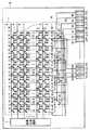
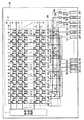
図3は、図1および図2に示したカラー液晶表示装置の組立部品であるLCDモジュールの構成を示す回路ブロック図である。図3において、このLCDモジュールは、ガラス基板15と、その表面に形成された液晶パネル1、垂直走査回路7、1:3デマルチプレクサ20、検査用端子切換回路25、複数(たとえば240)のデータ端子30.1〜30.4,…、R端子31、G端子32、B端子33、制御端子34、偶数データ端子35、および奇数データ端子36を備える。
【0016】
端子30.1〜30.4,…,31〜36は、ガラス基板15の1辺に沿って所定のピッチで配置される。検査時は、端子31〜36の各々はプローブを介して検査装置に接続される。検査後は、端子30.1〜30.4,…,31〜36はFPCに接続される。データ端子30.1〜30.4,…の各々には、FPCから階調電位VGが与えられる。R端子31には、R用のデータ線6を選択するための信号φRが与えられる。G端子32には、G用のデータ線6を選択するための信号φGが与えられる。B端子33には、B用のデータ線6を選択するための信号φBが与えられる。制御端子34には、制御信号φCが与えられる。偶数データ端子35には、偶数データ信号DEが与えられる。奇数データ端子36には、奇数データ信号DOが与えられる。
【0017】
1:3デマルチプレクサ20は、液晶パネル1の240組のR用データ線6、G用データ線6およびB用データ線6に対応して設けられた240組のN型TFT21〜23を含む。N型TFT21〜23は、それぞれ対応の組のR用データ線6、G用データ線6およびB用データ線6の一方端と対応のデータ端子(たとえば30.1)との間に接続され、そのゲートはそれぞれR端子31、G端子32およびB端子33に接続される。
【0018】
信号φR,φG,φBのうちの信号φRが「H」レベルにされると、各N型TFT21が導通し、各R用データ線6と対応のデータ端子とが結合される。信号φR,φG,φBのうちの信号φGが「H」レベルにされると、各N型TFT22が導通し、各G用データ線6と対応のデータ端子とが結合される。信号φR,φG,φBのうちの信号φBが「H」レベルにされると、各N型TFT23が導通し、各B用データ線6と対応のデータ端子とが結合される。
【0019】
検査用端子切換回路25は、240組のR用データ線6、G用データ線6およびB用データ線6のうちの各奇数番の組に対応して設けられたN型TFT26と、各偶数番の組に対応して設けられたN型TFT27とを含む。各N型TFT26は、対応のN型TFT21〜23のドレインと奇数データ線36との間に接続され、そのゲートは制御端子34に接続される。各N型TFT27は、対応のN型TFT21〜23のドレインと偶数データ端子35との間に接続され、そのゲートは制御端子34に接続される。
【0020】
制御信号φCが「H」レベルにされると、N型TFT26,27が導通し、奇数番目の組のN型TFT21〜23のドレインと奇数データ端子36が接続されるとともに、偶数番目の組のN型TFT21〜23のドレインと偶数データ端子35が接続される。
【0021】
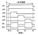
図4は、図3に示したLCDモジュールの検査方法を示すタイムチャートである。検査時は、端子31〜36の各々は、プローブを介して検査装置に接続される。ある時刻t0において複数の走査線4のうちのいずれかの走査線4が選択され、その走査線4の電位VHが「H」レベルに立上げられる。これにより、その走査線4に対応する各N型TFT11が導通し、各データ線6が導通したN型TFT11を介して液晶セル2に接続される。また時刻t0において制御信号φCが「H」レベルに立上げられてN型TFT26,27が導通し、奇数番の組のN型TFT21〜23のドレインがN型TFT26を介して奇数データ端子36に接続されるとともに、偶数番の組のN型TFT21〜23のドレインがN型TFT27を介して偶数データ端子35に接続される。
【0022】
次いで時刻t1において信号φRが「H」レベルに立上げられて各N型TFT21が導通し、各奇数番のR用データ線6がN型TFT21,26を介して奇数データ端子36に接続されるとともに、各偶数番のR用データ線6がN型TFT21,27を介して偶数データ端子35に接続される。また時刻t1において奇数データ信号DOが「L」レベルに立下げられるとともに偶数データ信号DEが「H」レベルに立上げられ、各奇数番のR用データ線6が「L」レベルにされるとともに各偶数番のR用データ線6が「H」レベルにされる。時刻t1から所定時間経過後に信号φRが「L」レベルに立下げられて各N型TFT21が非導通になり、選択された走査線4に対応する各R用液晶セル2へのデータ信号の書込が終了する。
【0023】
次に、時刻t2において信号φGが「H」レベルに立上げられて各N型TFT22が導通し、各奇数番のG用データ線6がN型TFT22,26を介して奇数データ端子36に接続されるとともに、各偶数番のG用データ線6がN型TFT22,27を介して偶数データ端子35に接続される。また時刻t2において奇数データ信号DOが「H」レベルに立上げられるとともに偶数データ信号DEが「L」レベルに立下げられ、各奇数番のG用データ線6が「H」レベルにされるとともに各偶数番のG用データ線6が「L」レベルにされる。時刻t2から所定時間経過後に信号φGが「L」レベルに立下げられて各N型TFT22が非導通になり、選択された走査線4に対応する各G用液晶セル2へのデータ信号の書込が終了する。
【0024】
次いで時刻t3において信号φBが「H」レベルに立上げられて各N型TFT23が導通し、各奇数番のB用データ線6がN型TFT23,26を介して奇数データ端子36に接続されるとともに、各偶数番のB用データ線6がN型TFT23,27を介して偶数データ端子35に接続される。また時刻t3において奇数データ信号DOが「L」レベルに立下げられるとともに偶数データ信号DEが「H」レベルに立下げられ、各奇数番のB用データ線6が「L」レベルにされるとともに各偶数番のB用データ線6が「H」レベルにされる。時刻t3から所定時間経過後に信号φBが「L」レベルに立下げられて各N型TFT23が非導通になり、選択された走査線4に対応する各B用液晶セル2へのデータ信号の書込が終了する。次に、時刻t4において走査線4の電位VHが「L」レベルに立下げられ、1本の走査線4に対応する各液晶セル2へのデータ信号の書込が終了する。
【0025】
以上の動作を各走査線4ごとに行なうことにより、液晶パネル1の全液晶セル2に「H」レベルまたは「L」レベルのデータ信号を書込むことができる。液晶パネル1が正常か否かは、たとえば各液晶セル2の光透過率を検出することにより判定される。たとえば隣接する2本のデータ線6が短絡している場合は、それらのデータ線6に対応する各液晶セル2には、「H」レベルと「L」レベルの間の中間レベルの電位が書込まれ、その液晶セル2は正常なデータ線6に対応する液晶セル2と異なる光透過率を示す。したがって、液晶パネル1が正常が否かを容易に判定することができる。
【0026】
検査において正常と判定されたLCDモジュールの端子30.1〜30.4,…,31〜36は、FPCに接続される。端子34〜36の各々は、FPCにより、N型TFT26,27を非導通にするような電位(たとえば接地電位GND)に固定される。階調電位VGの書込は、図4で示したデータ信号DE,DOの書込と同様に行なわれる。すなわち、図4の時刻t1〜t2の間は、データ端子30.1〜30.4,…の各々にR用階調電位VGが与えられ、R用液晶セル2の各々にR用階調電位VGが書込まれる。時刻t2〜t3の間は、データ端子30.1〜30.4,…の各々にG用階調電位VGが与えられ、G用液晶セル2の各々にG用階調電位VGが書込まれる。時刻t3〜t4の間は、データ端子30.1〜31.4,…の各々にB用階調電位VGが与えられ、B用液晶セル2の各々にB用階調電位VGが書込まれる。このようにして、液晶パネル1の各液晶セル2に階調電位VGが書込まれ、液晶パネル1の1つのカラー画像が表示される。
【0027】
この実施の形態1では、各奇数番の組のN型TFT21〜23のドレインと奇数データ端子36の間にN型TFT26を接続し、各偶数番の組のN型TFT21〜23のドレインと偶数データ端子35の間にN型TFT27を接続し、N型TFT26,27のゲートを制御端子34に接続する。検査時はN型TFT26,27を導通させて端子35,36に検査用のデータ信号DE,DOを与え、通常動作時はN型TFT26,27を非導通状態に固定する。したがって、検査時に必要な端子の数が少なくてすみ、検査装置の低コスト化を図ることができる。また、複数のLCDモジュールの複数の奇数データ端子36を互いに接続するとともに複数の偶数データ端子35を互いに接続した場合でも、各LCDモジュール用の制御信号φCのレベルを制御することにより、各LCDモジュールを個別に正確に検査することができる。
【0028】
なお、液晶パネル1は、ガラス基板15表面の所定領域に走査線4、データ線6、N型TFT11およびキャパシタ12を含むアレイ基板を形成した後に、そのアレイ基板の表面に液晶を介して対向基板を配置することにより形成される。実施の形態1では、液晶パネル1の組立後に液晶セル2の光透過率を検査することとしたが、液晶パネル1の組立前すなわち対向基板を配置する前の状態で、キャパシタ12の電荷量をモニタリングすることによりアレイ基板を検査してもよい。
【0029】
また、この実施の形態1では、検査用端子切換回路25をN型TFTで構成したが、P型TFTで構成してもよいし、N型TFTおよびP型TFTの並列接続体すなわちトランスファーゲートで接続してもよい。
【0030】
また、図5に示すように、検査時に使用する端子31〜36の各々のサイズをデータ端子30.1〜30.4,…の各々のサイズよりも大きくするとよい。これにより、プローブの位置精度を低下させることができ、検査装置のコストダウンを図ることができる。
【0031】
また、図6に示すように、検査時に使用する端子31〜36のピッチをデータ端子30.1〜30.4,…のピッチよりも大きくするとよい。この場合も、プローブの位置精度を低下させることができ、検査装置のコストダウンを図ることができる。また、図5の変更例と図6の変更例を組合せ、検査時に使用する端子31〜36の大きさおよびピッチをデータ端子30.1〜30.4,…の大きさおよびピッチよりも大きくすると、検査装置の一層のコストダウンを図ることができる。
【0032】
[実施の形態2]
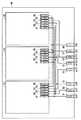
図7は、この発明の実施の形態2によりLCDモジュールの検査方法を説明するための図である。図7において、この検査方法では、ガラス基板40の表面に複数(図では3つ)のLCDモジュール41〜43が形成される。LCDモジュール41〜43の各々は、図3で示したものと同じである。LCDモジュール41〜43の各々の検査時に使用される端子31〜36は、ガラス基板40の1辺に対向して配置される。また、ガラス基板40のその1辺に沿って、R端子51、G端子52、B端子53、制御端子54〜56、偶数データ端子57、および奇数データ端子58が配置される。
【0033】
LCDモジュール41〜43のR端子31は、ともにR端子51に接続される。LCDモジュール41〜43のG端子32は、ともにG端子52に接続される。LCDモジュール41〜43のB端子33は、ともにB端子53に接続される。LCDモジュール41〜43の制御端子34は、ともに制御端子54〜56に接続される。LCDモジュール41〜43の偶数データ端子35は、ともに偶数データ端子57に接続される。LCDモジュール41〜43の奇数データ端子36は、ともに奇数データ端子58に接続される。
【0034】
検査時は、端子51〜58の各々がプローブを介して検査装置に接続される。端子51〜58には、それぞれ信号φR,φG,φB,φC1,φC2,φC3,DE,DOが与えられる。LCDモジュール41〜43を検査する場合は、それぞれ制御信号φC1〜φC3が「H」レベルにされる。LCDモジュール41〜43の各々は、実施の形態1と同じ方法で検査される。検査の終了後は、LCDモジュール41〜43の各々はガラス基板40から切出される。このとき、LCDモジュール41〜43の各々は、不要となった端子51〜58および配線から切離される。
【0035】
この実施の形態2では、1回のプロービングで複数のLCDモジュール41〜43を検査できるので、分断されたLCDモジュールを1つずつ検査する場合に比べ、プロービングの回数が少なくてすみ、プロービングの切換に必要な時間が短くてすむ。また、プロービングの回数が少なくてすむので、プローブの磨耗や折れ曲がりを軽減することができ、プローブの寿命を延ばすことができる。したがって、テストコストの大幅な低減化を図ることができる。
【0036】
なお、この実施の形態2でも、液晶パネル1を組立てる前の状態で、キャパシタ12の電荷量をモニタリングすることにより各アレイ基板を検査してもよい。
【0037】
[実施の形態3]
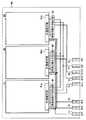
図8は、この発明の実施の形態3によるLCDモジュールの検査方法を説明するための図である。図8において、この検査方法では、ガラス基板60の表面に複数(図では3つ)のLCDモジュール61〜63が形成される。LCDモジュール61〜63の外部端子部61a〜61cは、ガラス基板60の1辺に対向して配置される。LCDモジュール61〜63の外部端子部61a〜61cに沿って、それぞれ検査用端子切換回路64〜66が設けられる。また、ガラス基板60のその1辺に沿って、R端子71、G端子72、B端子73、制御端子74〜76、偶数データ端子77、および奇数データ端子78が設けられる。
【0038】
図9は、LCDモジュール61の構成を示す回路ブロック図であって、図3と対比される図である。図9を参照して、LCDモジュール61が図3のLCDモジュールと異なる点は、検査用端子切換回路25、制御端子34、偶数データ端子35および奇数データ端子36が除去されている点である。外部端子部61aは、データ端子30.1〜30.4,…、R端子31、G端子32、およびB端子33を含む。ガラス基板15は、ガラス基板60の一部を構成している。LCDモジュール62,63もLCDモジュール61と同じ構成である。
【0039】
検査用端子切換回路64は、図10に示すように、奇数番のデータ端子30.1,30.3,…の各々に対応して設けられたN型TFT26と、偶数番のデータ端子30.2,30.4,…の各々に対応して設けられN型TFT27とを含む。各N型TFT26は、対応の奇数番のデータ端子と奇数データ端子78との間に接続され、そのゲートは制御端子74に接続される。各N型TFT27は、対応の偶数番のデータ端子と偶数データ端子77との間に接続され、そのゲートは制御端子74に接続される。なお、図10では、制御端子75,76の図示は省略されている。検査用端子切換回路65,66も検査用端子切換回路64と同じ構成である。ただし、検査用端子切換回路65のN型TFT26,27のゲートは制御端子75に接続され、検査用端子切換回路66のN型TFT26,27のゲートは制御端子76に接続される。
【0040】
検査時は、端子71〜78の各々がプローブを介して検査装置に接続される。端子71〜78には、それぞれ信号φR,φG,φB,φC1,φC2,φC3,DE,DOが与えられる。LCDモジュール61〜63を検査する場合は、それぞれ制御信号φC1〜φC3が「H」レベルにされる。LCDモジュール61〜63の各々は、実施の形態1と同様に検査される。検査の終了後は、LCDモジュール61〜63の各々はガラス基板60から切出される。このとき、LCDモジュール61〜63の各々は、不要となった検査用端子切換回路64〜66、端子71〜78および配線から切離される。
【0041】
この実施の形態3では、実施の形態2と同じ効果が得られる他、不要となったN型TFT26,27を非導通状態に固定する処置(N型TFT26,27のゲートおよびドレインに接地電位GNDを印加すること)が不要となる。また、LCDモジュールの構成が簡単になる。
【0042】
なお、この実施の形態3では、ガラス基板60上に複数のLCDモジュール61〜63を設けた場合について説明したが、図10から分かるように、この検査方法は、ガラス基板60上に1つのLCDモジュール61を設けた場合でも有効である。
【0043】
[実施の形態4]
図11は、この発明の実施の形態4によるLCDモジュールの構成を示す回路ブロック図であって、図3と対比される図である。図11を参照して、このLCDモジュールが図3のLCDモジュールと異なる点は、端子34〜36と検査用端子切換回路25の間の3本の配線がCOG(chip on glass)実装領域80を通過し、3本の配線のCOG実装領域80内の所定の位置にパッド81〜83がそれぞれ設けられている点である。検査の終了後には、COG実装領域80を覆うようにして半導体チップが実装される。このとき、半導体チップの接地電位GNDの電極が3つのパッド81〜83と導通状態にされ、パッド81〜83は接地電位GNDに固定される。半導体チップには、図示しない電源端子および接地端子より、電源電位VDDおよび接地電位GNDが与えられる。半導体チップは、DC−DCコンバータなどを含んでいる。
【0044】
図12は、COG実装領域80に実装された半導体チップ90の一部を示す断面図である。図12において、ガラス基板15の表面に絶縁膜92が形成され、絶縁膜92の表面に金属配線93が形成される。この金属配線93は、奇数データ端子36および各N型TFT26のドレインに接続される。
【0045】
金属配線93を覆うようにして絶縁膜94が形成され、絶縁膜94の所定領域に開口部が形成され、金属配線93の所定部分が露出される。絶縁膜94の開口部を覆うようにして金属端子であるパッド83が形成される。パッド83の表面に異方性導電樹脂95が塗布され、半導体チップ90の接地端子であるバンプ電極91がパッド83上に位置するように半導体チップ90が搭載される。これにより、バンプ電極91とパッド83は電気的に接続される。
【0046】
この実施の形態4では、検査後に半導体チップ90を実装することにより、検査用端子切換回路25のN型TFT26,27を非導通状態に固定する。したがって、LCDモジュールの外部から端子34〜36に接地電位GNDを与える必要がなくなるので、FPCの端子数を少なくすることができ、FPCの幅を狭くすることができる。
【0047】
なお、図13に示すように、端子34〜36をCOG実装領域80内に設けてもよい。端子34〜36は、半導体チップ90の実装により、接地電位GNDに固定される。この変更例では、実施の形態4と同じ効果が得られる他、パッド81〜83を別途設ける必要がない。
【0048】
今回開示された実施の形態はすべての点で例示であって制限的なものではないと考えられるべきである。本発明の範囲は上記した説明ではなくて特許請求の範囲によって示され、特許請求の範囲と均等の意味および範囲内でのすべての変更が含まれることが意図される。
【0049】
【発明の効果】
以上のように、この発明に係る画像表示装置では、複数行複数列に配置された複数の画素表示回路と、それぞれ複数行に対応して設けられた複数の走査線と、それぞれ複数列に対応して設けられた複数のデータ線とを含み、各データ線グループはそれぞれR,G,Bに対応する3本のデータ線を有する画像表示パネルと、それぞれ複数のデータ線グループに対応して設けられ、各々が第1〜第3のトランジスタを含む複数のトランジスタグループを含み、各トランジスタグループの第1〜第3のトランジスタの第1の電極はそれぞれ対応のデータ線グループの3本のデータ線に接続され、各トランジスタグループの第1〜第3のトランジスタの第2の電極は互いに接続されたデマルチプレクサと、それぞれ複数のトランジスタグループに対応して設けられ、各々の第1の電極が対応のトランジスタグループの第1〜第3のトランジスタの第2の電極に接続され、画像表示パネルの通常動作時に非導通にされる複数の検査トランジスタと、各トランジスタグループの第1のトランジスタのゲートに接続されたR端子と、各トランジスタグループの第2のトランジスタのゲートに接続されたG端子と、各トランジスタグループの第3のトランジスタのゲートに接続されたB端子と、複数の検査トランジスタのうちの各奇数番の検査トランジスタの第2の電極に接続された第1の検査端子と、複数の検査トランジスタのうちの各偶数番の検査トランジスタの第2の電極に接続された第2の検査端子と、複数の検査トランジスタのゲートに接続され、画像表示パネルの検査時に複数の検査トランジスタを制御するための制御信号を受ける制御端子と、それぞれ複数のトランジスタグループに対応して設けられ、各々が、対応のトランジスタグループの第1〜第3のトランジスタの第2の電極に接続され、通常動作時に画素表示回路に画素を表示させるための画素電位を受ける複数のデータ端子とが設けられる。したがって、R端子、G端子、B端子、第1の検査端子、第2の検査端子および制御端子を検査装置に接続すれば検査できるので、検査に使用する端子の数が少なくてすみ、検査装置のコストダウンを図ることができる。また、複数の画像表示装置の複数の第1の検査端子を互いに接続するとともに複数の第2の検査端子を互いに接続した場合でも、画像表示装置を1つずつ正確に検査することができる。
【図面の簡単な説明】
【図1】 この発明の実施の形態1によるカラー液晶画像装置の構成を示すブロック図である。
【図2】 図1に示した液晶セルに対応して設けられる液晶駆動回路の構成を示す回路図である。
【図3】 図1に示したカラー液晶表示装置の組立部品であるLCDモジュールの構成を示す回路ブロック図である。
【図4】 図3に示したLCDモジュールの検査方法を説明するためのタイムチャートである。
【図5】 実施の形態1の変更例を示す回路ブロック図である。
【図6】 実施の形態1の他の変更例を示す回路ブロック図である。
【図7】 この発明の実施の形態2によるLCDモジュールの検査方法を説明するための図である。
【図8】 この発明の実施の形態3によるLCDモジュールの検査方法を説明するための図である。
【図9】 図8に示したLCDモジュールの構成を示す回路ブロック図である。
【図10】 図8に示した検査用端子切換回路の構成を示す回路ブロック図である。
【図11】 この発明の実施の形態4によるLCDモジュールの構成を示す回路ブロック図である。
【図12】 図11に示したLCDモジュールへの半導体チップの実装方法を説明するための断面図である。
【図13】 実施の形態4の変更例を示す回路ブロック図である。
【符号の説明】
1 液晶パネル、2 液晶セル、3 画素、4 走査線、5 共通電位線、6データ線、7 垂直走査回路、8 水平走査回路、10 液晶駆動回路、11,21〜23,26,27 N型TFT、12 キャパシタ、15,40,60 ガラス基板、20 1:3デマルチプレクサ、25,64〜66 検査用端子切換回路、30 データ端子、31,51,71 R端子、32,52,72 G端子、33,53,73 B端子、34,54〜56,74〜76 制御端子、35,57,77 偶数データ端子、36,58,78 奇数データ端子、41〜43,61〜63 LCDモジュール、61a〜63a 外部端子部、80 COG実装領域、81〜83 パッド、90 半導体チップ、91 バンプ電極、92,94 絶縁膜、93 金属配線、95 異方性導電樹脂。[0001]
BACKGROUND OF THE INVENTION
The present invention relates to an image display device, and more particularly to an image display device formed on an insulating substrate and inspected before shipment.
[0002]
[Prior art]
In recent years, the resolution of liquid crystal panels has been increased, and the number of terminals for connecting a liquid crystal dispray (LCD) module and a flexible printed circuit board (FPC) has increased. Further, the miniaturization of the LCD module has been promoted, and the pitch of the terminals has been narrowed. The liquid crystal panel is inspected by applying a probe to each terminal. However, as the number of terminals is increased and the terminal pitch is reduced, the cost of the inspection apparatus is increased.
[0003]
As a method for reducing the cost of the inspection apparatus, an odd numbered data line of the liquid crystal panel is connected to one inspection terminal, and an even numbered data line is connected to another inspection terminal and two inspection terminals are used. There is a method of removing two terminals after inspection (see, for example, Patent Document 1).
[0004]
[Patent Document 1]
JP-A-5-5897
[0005]
[Problems to be solved by the invention]
If such two inspection terminals are provided in common for a plurality of liquid crystal panels, it is considered that the cost of the inspection apparatus can be further reduced. However, simply connecting each odd-numbered data line of a plurality of liquid crystal panels to one inspection terminal and connecting an even-numbered data line to the other inspection terminal can accurately inspect each liquid crystal panel individually. I can't.
[0006]
Therefore, a main object of the present invention is to provide an image display apparatus capable of accurately performing inspection at a low cost.
[0007]
[Means for Solving the Problems]
An image display device according to the present invention is an image display device formed on an insulating substrate, and a plurality of pixel display circuits arranged in a plurality of rows and a plurality of columns, and a plurality of pixel display circuits provided corresponding to the plurality of rows, respectively. Scanning lines and a plurality of data lines provided corresponding to a plurality of columns, respectively.Each data line group has three data lines corresponding to R, G, and B, respectively.An image display panel;Each is provided corresponding to a plurality of data line groups, each including a plurality of transistor groups including first to third transistors, and the first electrodes of the first to third transistors of each transistor group respectively correspond to each other. The second electrodes of the first to third transistors of each transistor group are provided corresponding to a plurality of transistor groups and to each of a plurality of transistor groups. , Each first electrode corresponding to the second electrode of the first to third transistors of the corresponding transistor groupA plurality of inspection transistors that are connected to each other and are rendered non-conductive during normal operation of the image display panel;An R terminal connected to the gate of the first transistor in each transistor group, a G terminal connected to the gate of the second transistor in each transistor group, and a gate of the third transistor in each transistor group B terminal;A first inspection terminal connected to the second electrode of each odd-numbered inspection transistor among the plurality of inspection transistors, and a second electrode of each even-numbered inspection transistor among the plurality of inspection transistors. Connected to the second inspection terminal and the gates of the plurality of inspection transistors,On the image display panelReceives control signals for controlling multiple test transistors during testingSystemControl terminals and multipleTransistor groupAre provided corresponding to each, Connected to the second electrodes of the first to third transistors of the corresponding transistor group,And a plurality of data terminals for receiving a pixel potential for causing the pixel display circuit to display pixels during normal operation..
[0008]
DETAILED DESCRIPTION OF THE INVENTION
[Embodiment 1]
FIG. 1 is a block diagram showing a configuration of a color liquid crystal display device according to
[0009]
The
[0010]
Three
[0011]
Each
[0012]
Returning to FIG. 1, the
[0013]
The
[0014]
When all the
[0015]
FIG. 3 is a circuit block diagram showing a configuration of an LCD module which is an assembly part of the color liquid crystal display device shown in FIGS. 3, this LCD module includes a
[0016]
The terminals 30.1 to 30.4,..., 31 to 36 are arranged at a predetermined pitch along one side of the
[0017]
The 1: 3
[0018]
When signal φR among signals φR, φG, and φB is set to “H” level, each N-
[0019]
The inspection
[0020]
When the control signal φC is set to the “H” level, the N-
[0021]
FIG. 4 is a time chart showing an inspection method of the LCD module shown in FIG. At the time of inspection, each of the
[0022]
Next, at
[0023]
Next, at
[0024]
Next, at
[0025]
By performing the above operation for each
[0026]
The terminals 30.1 to 30.4,..., 31 to 36 of the LCD module determined to be normal in the inspection are connected to the FPC. Each of
[0027]
In the first embodiment, an N-
[0028]
The
[0029]
In the first embodiment, the inspection
[0030]
Further, as shown in FIG. 5, it is preferable that the size of each of the
[0031]
Further, as shown in FIG. 6, the pitch of the
[0032]
[Embodiment 2]
FIG. 7 is a diagram for explaining a method of inspecting an LCD module according to the second embodiment of the present invention. 7, in this inspection method, a plurality (three in the figure) of
[0033]
The
[0034]
At the time of inspection, each of the
[0035]
In the second embodiment, since a plurality of
[0036]
In the second embodiment as well, each array substrate may be inspected by monitoring the charge amount of the
[0037]
[Embodiment 3]
FIG. 8 is a diagram for explaining an inspection method for an LCD module according to
[0038]
FIG. 9 is a circuit block diagram showing a configuration of the
[0039]
As shown in FIG. 10, the inspection
[0040]
At the time of inspection, each of the
[0041]
In the third embodiment, the same effects as those of the second embodiment can be obtained, and the N-
[0042]
In the third embodiment, the case where a plurality of
[0043]
[Embodiment 4]
FIG. 11 is a circuit block diagram showing a configuration of an LCD module according to
[0044]
FIG. 12 is a cross-sectional view showing a part of the
[0045]
An insulating
[0046]
In the fourth embodiment, by mounting the
[0047]
Note that the
[0048]
The embodiment disclosed this time should be considered as illustrative in all points and not restrictive. The scope of the present invention is defined by the terms of the claims, rather than the description above, and is intended to include any modifications within the scope and meaning equivalent to the terms of the claims.
[0049]
【The invention's effect】
As described above, in the image display device according to the present invention, a plurality of pixel display circuits arranged in a plurality of rows and a plurality of columns, a plurality of scanning lines provided corresponding to the plurality of rows, and a plurality of columns respectively. Including multiple data linesEach data line group has three data lines corresponding to R, G, and B, respectively.An image display panel;Each is provided corresponding to a plurality of data line groups, each including a plurality of transistor groups including first to third transistors, and the first electrodes of the first to third transistors of each transistor group respectively correspond to each other. The second electrodes of the first to third transistors of each transistor group are provided corresponding to a plurality of transistor groups and to each of a plurality of transistor groups. , Each first electrode corresponding to the second electrode of the first to third transistors of the corresponding transistor groupA plurality of inspection transistors that are connected to each other and are rendered non-conductive during normal operation of the image display panel;An R terminal connected to the gate of the first transistor in each transistor group, a G terminal connected to the gate of the second transistor in each transistor group, and a gate of the third transistor in each transistor group B terminal;A first inspection terminal connected to the second electrode of each odd-numbered inspection transistor among the plurality of inspection transistors, and a second electrode of each even-numbered inspection transistor among the plurality of inspection transistors. A second inspection terminal and a plurality ofInspectionConnected to the gate of the transistor,On the image display panelReceives control signals for controlling multiple test transistors during testingSystemControl terminals and multipleTransistor groupAre provided corresponding to each, Connected to the second electrodes of the first to third transistors of the corresponding transistor group,And a plurality of data terminals for receiving a pixel potential for displaying the pixel on the pixel display circuit during normal operation.Be. Therefore,R terminal, G terminal, B terminal,First inspection terminal, second inspection terminal andSystemSince the inspection can be performed by connecting the control terminal to the inspection apparatus, the number of terminals used for the inspection can be reduced, and the cost of the inspection apparatus can be reduced. Further, even when a plurality of first inspection terminals of a plurality of image display devices are connected to each other and a plurality of second inspection terminals are connected to each other, the image display devices can be accurately inspected one by one.
[Brief description of the drawings]
FIG. 1 is a block diagram showing a configuration of a color liquid crystal image device according to
FIG. 2 is a circuit diagram showing a configuration of a liquid crystal driving circuit provided corresponding to the liquid crystal cell shown in FIG.
3 is a circuit block diagram showing a configuration of an LCD module that is an assembly part of the color liquid crystal display device shown in FIG. 1. FIG.
4 is a time chart for explaining an inspection method of the LCD module shown in FIG. 3; FIG.
FIG. 5 is a circuit block diagram showing a modification of the first embodiment.
FIG. 6 is a circuit block diagram showing another modification of the first embodiment.
FIG. 7 is a view for explaining an LCD module inspection method according to
FIG. 8 is a view for explaining an LCD module inspection method according to
9 is a circuit block diagram showing a configuration of the LCD module shown in FIG. 8. FIG.
10 is a circuit block diagram showing a configuration of the inspection terminal switching circuit shown in FIG. 8;
FIG. 11 is a circuit block diagram showing a configuration of an LCD module according to
12 is a cross-sectional view for explaining a method of mounting a semiconductor chip on the LCD module shown in FIG.
FIG. 13 is a circuit block diagram illustrating a modification of the fourth embodiment.
[Explanation of symbols]
1 liquid crystal panel, 2 liquid crystal cell, 3 pixels, 4 scanning lines, 5 common potential lines, 6 data lines, 7 vertical scanning circuit, 8 horizontal scanning circuit, 10 liquid crystal driving circuit, 11, 21-23, 26, 27 N type TFT, 12 capacitor, 15, 40, 60 glass substrate, 20 1: 3 demultiplexer, 25, 64 to 66 inspection terminal switching circuit, 30 data terminal, 31, 51, 71 R terminal, 32, 52, 72
Claims (6)
Translated fromJapanese複数行複数列に配置された複数の画素表示回路と、それぞれ前記複数行に対応して設けられた複数の走査線と、それぞれ前記複数列に対応して設けられ、予め複数のデータ線グループに分割された複数のデータ線とを含み、各データ線グループはそれぞれR,G,Bに対応する3本のデータ線を有する画像表示パネル、
それぞれ前記複数のデータ線グループに対応して設けられ、各々が第1〜第3のトランジスタを含む複数のトランジスタグループを含み、各トランジスタグループの第1〜第3のトランジスタの第1の電極はそれぞれ対応のデータ線グループの3本のデータ線に接続され、各トランジスタグループの第1〜第3のトランジスタの第2の電極は互いに接続されたデマルチプレクサ、
それぞれ前記複数のトランジスタグループに対応して設けられ、各々の第1の電極が対応のトランジスタグループの第1〜第3のトランジスタの第2の電極に接続され、前記画像表示パネルの通常動作時に非導通にされる複数の検査トランジスタ、
各トランジスタグループの第1のトランジスタのゲートに接続されたR端子、
各トランジスタグループの第2のトランジスタのゲートに接続されたG端子、
各トランジスタグループの第3のトランジスタのゲートに接続されたB端子、
前記複数の検査トランジスタのうちの各奇数番の検査トランジスタの第2の電極に接続された第1の検査端子、
前記複数の検査トランジスタのうちの各偶数番の検査トランジスタの第2の電極に接続された第2の検査端子、
前記複数の検査トランジスタのゲートに接続され、前記画像表示パネルの検査時に前記複数の検査トランジスタを制御するための制御信号を受ける制御端子、および
それぞれ前記複数のトランジスタグループに対応して設けられ、各々が、対応のトランジスタグループの第1〜第3のトランジスタの第2の電極に接続され、前記通常動作時に前記画素表示回路に画素を表示させるための画素電位を受ける複数のデータ端子を備える、画像表示装置。An image display device formed on an insulating substrate,
A plurality of pixel display circuits arranged in a plurality of rows and a plurality of columns, a plurality of scanning lines provided corresponding to the plurality of rows, and a plurality of scanning lines provided corresponding to the plurality of columns, respectively, An image display panel including a plurality of divided data lines, each data line group having three data lines corresponding to R, G, and B,
Each of the plurality of data line groups is provided corresponding to the plurality of data line groups, each including a plurality of transistor groups including first to third transistors, and the first electrodes of the first to third transistors of each transistor group are respectively A demultiplexer connected to the three data lines of the corresponding data line group, the second electrodes of the first to third transistors of each transistor group being connected to each other;
Each of the first electrodes is provided corresponding to the plurality of transistor groups, and each of the first electrodes is connected to the second electrodes of the first to third transistors of the corresponding transistor group. A plurality of test transistors made conductive,
An R terminal connected to the gate of the first transistor of each transistor group;
A G terminal connected to the gate of the second transistor of each transistor group;
A B terminal connected to the gate of the third transistor in each transistor group;
A first inspection terminal connected to a second electrode of each odd-numbered inspection transistor among the plurality of inspection transistors;
A second inspection terminal connected to a second electrode of each even-numbered inspection transistor of the plurality of inspection transistors;
Which is connected to the gate of the plurality of test transistors, provided in correspondence with the image display control signal receivingRu control terminals, and each of the plurality of transistors groups for controlling the plurality of test transistors during inspection of the panel , Each having a plurality of data terminals connected to the second electrodes of the first to third transistors of the corresponding transistor group and receiving a pixel potential for causing the pixel display circuit to display the pixels during the normal operation. , Image display device.
前記R端子、前記G端子、前記B端子、前記第1の検査端子、前記第2の検査端子および前記制御端子は前記複数のデータ端子のピッチよりも大きなピッチで配列されている、請求項1に記載の画像表示装置。The plurality of data terminals are arranged at a predetermined pitch,
Wherein R terminal, the G terminal, the B terminal, the first test terminal, the second test terminal and beforeSymbol control terminal are arranged at a pitch greater than the pitch of said plurality of data terminals, wherein Item 4. The image display device according to Item1 .
Priority Applications (5)
| Application Number | Priority Date | Filing Date | Title |
|---|---|---|---|
| JP2003061778AJP3964337B2 (en) | 2003-03-07 | 2003-03-07 | Image display device |
| TW092116621ATWI279633B (en) | 2003-03-07 | 2003-06-19 | Image display device using insulation substrate |
| US10/644,794US6982568B2 (en) | 2003-03-07 | 2003-08-21 | Image display device having inspection terminal |
| KR1020030075079AKR100561150B1 (en) | 2003-03-07 | 2003-10-27 | Image display device having inspection terminal |
| CNB2003101036958ACN1262870C (en) | 2003-03-07 | 2003-10-28 | Image display device equipment with checking terminal |
Applications Claiming Priority (1)
| Application Number | Priority Date | Filing Date | Title |
|---|---|---|---|
| JP2003061778AJP3964337B2 (en) | 2003-03-07 | 2003-03-07 | Image display device |
Related Child Applications (1)
| Application Number | Title | Priority Date | Filing Date |
|---|---|---|---|
| JP2007057603ADivisionJP4570633B2 (en) | 2007-03-07 | 2007-03-07 | Image display device |
Publications (3)
| Publication Number | Publication Date |
|---|---|
| JP2004271847A JP2004271847A (en) | 2004-09-30 |
| JP2004271847A5 JP2004271847A5 (en) | 2006-02-02 |
| JP3964337B2true JP3964337B2 (en) | 2007-08-22 |
Family
ID=32923643
Family Applications (1)
| Application Number | Title | Priority Date | Filing Date |
|---|---|---|---|
| JP2003061778AExpired - LifetimeJP3964337B2 (en) | 2003-03-07 | 2003-03-07 | Image display device |
Country Status (5)
| Country | Link |
|---|---|
| US (1) | US6982568B2 (en) |
| JP (1) | JP3964337B2 (en) |
| KR (1) | KR100561150B1 (en) |
| CN (1) | CN1262870C (en) |
| TW (1) | TWI279633B (en) |
Families Citing this family (47)
| Publication number | Priority date | Publication date | Assignee | Title |
|---|---|---|---|---|
| JP3866783B2 (en) | 1995-07-25 | 2007-01-10 | 株式会社 日立ディスプレイズ | Liquid crystal display |
| KR100491560B1 (en)* | 2003-05-06 | 2005-05-27 | 엘지.필립스 엘시디 주식회사 | Method and Apparatus for Testing Liquid Crystal Display Device |
| JP2005049519A (en)* | 2003-07-31 | 2005-02-24 | Toshiba Matsushita Display Technology Co Ltd | Display device |
| US8013816B2 (en)* | 2004-06-30 | 2011-09-06 | Samsung Mobile Display Co., Ltd. | Light emitting display |
| JP4630598B2 (en)* | 2004-08-06 | 2011-02-09 | 東芝モバイルディスプレイ株式会社 | Display device, display device inspection method, and display device inspection device |
| JP4476737B2 (en)* | 2004-08-06 | 2010-06-09 | 東芝モバイルディスプレイ株式会社 | Display device, display device inspection method, and display device inspection device |
| JP2006091239A (en) | 2004-09-22 | 2006-04-06 | Seiko Epson Corp | Electro-optical device substrate, electro-optical device, and inspection method |
| TWI333094B (en)* | 2005-02-25 | 2010-11-11 | Au Optronics Corp | System and method for display testing |
| JP4633536B2 (en)* | 2005-05-19 | 2011-02-16 | 三菱電機株式会社 | Display device |
| KR101137885B1 (en)* | 2005-06-15 | 2012-04-25 | 엘지디스플레이 주식회사 | Liquid Crystal Display Device and Testing Method thereof |
| CN100464238C (en)* | 2005-07-01 | 2009-02-25 | 中华映管股份有限公司 | Active element array and detection method of active element array |
| KR100830383B1 (en)* | 2005-08-18 | 2008-05-20 | 세이코 엡슨 가부시키가이샤 | Electro-optical devices, their inspection methods, and electronic devices |
| JP5194382B2 (en)* | 2005-08-18 | 2013-05-08 | セイコーエプソン株式会社 | Electro-optical device and electronic apparatus |
| TWI309813B (en)* | 2005-12-23 | 2009-05-11 | Au Optronics Corp | Display device and pixel testing method thereof |
| CN100399175C (en)* | 2005-12-29 | 2008-07-02 | 友达光电股份有限公司 | Active component array substrate |
| CN100456114C (en)* | 2006-01-16 | 2009-01-28 | 友达光电股份有限公司 | Display device and pixel testing method thereof |
| JP4561647B2 (en)* | 2006-02-02 | 2010-10-13 | セイコーエプソン株式会社 | Electro-optical device substrate, electro-optical device, and inspection method |
| JP2007248502A (en)* | 2006-03-13 | 2007-09-27 | Epson Imaging Devices Corp | Method of manufacturing display apparatus, and display apparatus |
| US20070290375A1 (en)* | 2006-06-01 | 2007-12-20 | Chin-Hai Huang | Active device array mother substrate |
| CN101097304B (en)* | 2006-06-27 | 2011-07-13 | 中华映管股份有限公司 | Active Component Array Motherboard |
| TW200801755A (en)* | 2006-06-30 | 2008-01-01 | Innolux Display Corp | Thin film transistor substrate and liquid crystal display panel using the same |
| JP2008026507A (en)* | 2006-07-20 | 2008-02-07 | Sony Corp | Display device and method of inspecting display device |
| KR20080010551A (en)* | 2006-07-27 | 2008-01-31 | 삼성전자주식회사 | Drive device for display device and display device including same |
| JP4984815B2 (en)* | 2006-10-19 | 2012-07-25 | セイコーエプソン株式会社 | Manufacturing method of electro-optical device |
| KR101304415B1 (en)* | 2007-01-25 | 2013-09-05 | 삼성디스플레이 주식회사 | Display device |
| JP5138999B2 (en)* | 2007-08-01 | 2013-02-06 | 三菱電機株式会社 | Display device |
| JP5428299B2 (en)* | 2008-03-18 | 2014-02-26 | セイコーエプソン株式会社 | Electro-optical device and electronic apparatus |
| CN102109688B (en)* | 2009-12-29 | 2014-02-05 | 上海天马微电子有限公司 | Liquid crystal display panel, array substrate and driving line defect detection method |
| JP5570246B2 (en)* | 2010-02-26 | 2014-08-13 | 三菱電機株式会社 | Liquid crystal display |
| CN102566169B (en) | 2010-12-31 | 2015-02-25 | 上海天马微电子有限公司 | Detection device of liquid crystal display device and test method thereof |
| JP2012208301A (en)* | 2011-03-29 | 2012-10-25 | Seiko Epson Corp | Liquid crystal device and projection type display device |
| CN102368133B (en)* | 2011-10-14 | 2013-11-20 | 深圳市华星光电技术有限公司 | Liquid crystal array and liquid crystal display panel |
| CN102495503A (en)* | 2011-11-22 | 2012-06-13 | 深圳市华星光电技术有限公司 | Array substrate and driving method thereof |
| JP6051011B2 (en)* | 2012-10-22 | 2016-12-21 | 株式会社ジャパンディスプレイ | Liquid crystal display device and manufacturing method thereof |
| KR101403127B1 (en) | 2012-11-23 | 2014-06-03 | 엘지디스플레이 주식회사 | Display Panel and Method for Testing Display Panel |
| CN103091918B (en)* | 2013-01-18 | 2016-01-13 | 北京京东方光电科技有限公司 | Array base palte, display device and detection method |
| KR20140094723A (en) | 2013-01-21 | 2014-07-31 | 삼성디스플레이 주식회사 | Thin film transistor substrate, method of inspecting the same and liquid crystal display including the same |
| US11457531B2 (en)* | 2013-04-29 | 2022-09-27 | Samsung Display Co., Ltd. | Electronic component, electric device including the same, and bonding method thereof |
| CN103345080B (en)* | 2013-07-10 | 2017-01-25 | 深圳市华星光电技术有限公司 | Rapid test switching device and corresponding TFT-LCD array substrate |
| CN104616612B (en)* | 2015-02-26 | 2018-05-25 | 上海和辉光电有限公司 | Displayer, its test suite and its defect test method |
| JP6681926B2 (en) | 2016-02-10 | 2020-04-15 | シャープ株式会社 | Active matrix substrate and display panel |
| CN106057112B (en)* | 2016-08-09 | 2019-04-16 | 武汉华星光电技术有限公司 | Circuit and liquid crystal display substrate are tested at box |
| CN106646953A (en)* | 2017-02-28 | 2017-05-10 | 武汉华星光电技术有限公司 | Liquid crystal display panel |
| US20210005701A1 (en)* | 2018-03-02 | 2021-01-07 | Sharp Kabushiki Kaisha | Display device |
| CN108897160A (en)* | 2018-08-06 | 2018-11-27 | 深圳市华星光电技术有限公司 | Liquid crystal display panel and its alignment method |
| CN109407321B (en)* | 2018-12-04 | 2021-03-19 | 厦门天马微电子有限公司 | Display device |
| CN112927637A (en)* | 2019-12-06 | 2021-06-08 | 群创光电股份有限公司 | Method for manufacturing electronic device and electronic device |
Family Cites Families (13)
| Publication number | Priority date | Publication date | Assignee | Title |
|---|---|---|---|---|
| JP2594358B2 (en) | 1989-06-16 | 1997-03-26 | 松下電子工業株式会社 | Image display device |
| JP2792634B2 (en) | 1991-06-28 | 1998-09-03 | シャープ株式会社 | Active matrix substrate inspection method |
| CN100576306C (en)* | 1995-02-01 | 2009-12-30 | 精工爱普生株式会社 | Liquid crystal display device |
| JPH10104647A (en) | 1996-09-30 | 1998-04-24 | Advanced Display:Kk | Liquid crystal display device |
| KR100281058B1 (en)* | 1997-11-05 | 2001-02-01 | 구본준, 론 위라하디락사 | Liquid Crystal Display |
| KR100341128B1 (en)* | 1999-06-30 | 2002-06-20 | 주식회사 현대 디스플레이 테크놀로지 | method for testing display quality of LCD |
| JP2001235725A (en) | 2000-02-24 | 2001-08-31 | Victor Co Of Japan Ltd | Liquid crystal display device |
| JP5053479B2 (en)* | 2000-09-14 | 2012-10-17 | 株式会社ジャパンディスプレイセントラル | Matrix array substrate and manufacturing method thereof |
| JP2002098999A (en) | 2000-09-26 | 2002-04-05 | Toshiba Corp | Liquid crystal display |
| KR100494685B1 (en)* | 2000-12-30 | 2005-06-13 | 비오이 하이디스 테크놀로지 주식회사 | Method for testing defect of lcd panel wiring |
| KR100806885B1 (en)* | 2001-06-12 | 2008-02-22 | 삼성전자주식회사 | Manufacturing Method Of Liquid Crystal Display |
| JP4006304B2 (en)* | 2002-09-10 | 2007-11-14 | 株式会社 日立ディスプレイズ | Image display device |
| JP3628014B1 (en)* | 2003-09-19 | 2005-03-09 | ウインテスト株式会社 | Display device and inspection method and device for active matrix substrate used therefor |
- 2003
- 2003-03-07JPJP2003061778Apatent/JP3964337B2/ennot_activeExpired - Lifetime
- 2003-06-19TWTW092116621Apatent/TWI279633B/ennot_activeIP Right Cessation
- 2003-08-21USUS10/644,794patent/US6982568B2/ennot_activeExpired - Lifetime
- 2003-10-27KRKR1020030075079Apatent/KR100561150B1/ennot_activeExpired - Lifetime
- 2003-10-28CNCNB2003101036958Apatent/CN1262870C/ennot_activeExpired - Lifetime
Also Published As
| Publication number | Publication date |
|---|---|
| TWI279633B (en) | 2007-04-21 |
| CN1527104A (en) | 2004-09-08 |
| US6982568B2 (en) | 2006-01-03 |
| TW200417802A (en) | 2004-09-16 |
| US20040174183A1 (en) | 2004-09-09 |
| KR20040079820A (en) | 2004-09-16 |
| KR100561150B1 (en) | 2006-03-15 |
| CN1262870C (en) | 2006-07-05 |
| JP2004271847A (en) | 2004-09-30 |
Similar Documents
| Publication | Publication Date | Title |
|---|---|---|
| JP3964337B2 (en) | Image display device | |
| JP4657598B2 (en) | Liquid crystal display device and inspection method thereof | |
| US7777854B2 (en) | Liquid crystal display, testing method thereof and manufacturing method thereof | |
| US7456647B2 (en) | Liquid crystal display panel and testing and manufacturing methods thereof | |
| KR100360157B1 (en) | Array substrate and method for checking array substrate | |
| KR101791192B1 (en) | Display Apparatus and Method for Testing The Same | |
| US20090231255A1 (en) | Display panel and display device having the panel | |
| US20070080913A1 (en) | Display device and testing method for display device | |
| JP2004310024A5 (en) | ||
| US9298055B2 (en) | Array substrate, method of disconnection inspecting gate lead wire and source lead wire in the array substrate, method of inspecting the array substrate, and liquid crystal display device | |
| JP5599501B2 (en) | Image display panel inspection method | |
| JP2005010282A (en) | Image display device | |
| US6985340B2 (en) | Semiconductor device with protection circuit protecting internal circuit from static electricity | |
| KR20070093540A (en) | Display device | |
| JP4570633B2 (en) | Image display device | |
| JP2008065152A (en) | Liquid crystal display panel, inspection apparatus, and inspection method | |
| KR20080022354A (en) | Liquid crystal display device | |
| JP5570246B2 (en) | Liquid crystal display | |
| KR100973803B1 (en) | Liquid crystal display | |
| KR101157248B1 (en) | Mass production system checking structure of liquid crystal display device | |
| JPH11202369A (en) | Liquid crystal display device and manufacturing method thereof | |
| KR20080022356A (en) | LCD and Manufacturing Method of LCD | |
| KR100978253B1 (en) | Thin film transistor array substrate | |
| KR101108774B1 (en) | Liquid Crystal Display device and method for fabricating the same | |
| KR20080018584A (en) | Inspection device of liquid crystal display |
Legal Events
| Date | Code | Title | Description |
|---|---|---|---|
| A521 | Request for written amendment filed | Free format text:JAPANESE INTERMEDIATE CODE: A523 Effective date:20051205 | |
| A621 | Written request for application examination | Free format text:JAPANESE INTERMEDIATE CODE: A621 Effective date:20051205 | |
| A871 | Explanation of circumstances concerning accelerated examination | Free format text:JAPANESE INTERMEDIATE CODE: A871 Effective date:20060810 | |
| A975 | Report on accelerated examination | Free format text:JAPANESE INTERMEDIATE CODE: A971005 Effective date:20061011 | |
| A131 | Notification of reasons for refusal | Free format text:JAPANESE INTERMEDIATE CODE: A131 Effective date:20061017 | |
| A521 | Request for written amendment filed | Free format text:JAPANESE INTERMEDIATE CODE: A523 Effective date:20061213 | |
| A02 | Decision of refusal | Free format text:JAPANESE INTERMEDIATE CODE: A02 Effective date:20070116 | |
| A521 | Request for written amendment filed | Free format text:JAPANESE INTERMEDIATE CODE: A523 Effective date:20070307 | |
| A911 | Transfer to examiner for re-examination before appeal (zenchi) | Free format text:JAPANESE INTERMEDIATE CODE: A911 Effective date:20070323 | |
| TRDD | Decision of grant or rejection written | ||
| A01 | Written decision to grant a patent or to grant a registration (utility model) | Free format text:JAPANESE INTERMEDIATE CODE: A01 Effective date:20070515 | |
| A61 | First payment of annual fees (during grant procedure) | Free format text:JAPANESE INTERMEDIATE CODE: A61 Effective date:20070523 | |
| R150 | Certificate of patent or registration of utility model | Free format text:JAPANESE INTERMEDIATE CODE: R150 Ref document number:3964337 Country of ref document:JP Free format text:JAPANESE INTERMEDIATE CODE: R150 | |
| FPAY | Renewal fee payment (event date is renewal date of database) | Free format text:PAYMENT UNTIL: 20100601 Year of fee payment:3 | |
| FPAY | Renewal fee payment (event date is renewal date of database) | Free format text:PAYMENT UNTIL: 20110601 Year of fee payment:4 | |
| FPAY | Renewal fee payment (event date is renewal date of database) | Free format text:PAYMENT UNTIL: 20120601 Year of fee payment:5 | |
| FPAY | Renewal fee payment (event date is renewal date of database) | Free format text:PAYMENT UNTIL: 20130601 Year of fee payment:6 | |
| R250 | Receipt of annual fees | Free format text:JAPANESE INTERMEDIATE CODE: R250 | |
| R250 | Receipt of annual fees | Free format text:JAPANESE INTERMEDIATE CODE: R250 | |
| R250 | Receipt of annual fees | Free format text:JAPANESE INTERMEDIATE CODE: R250 | |
| R250 | Receipt of annual fees | Free format text:JAPANESE INTERMEDIATE CODE: R250 | |
| R250 | Receipt of annual fees | Free format text:JAPANESE INTERMEDIATE CODE: R250 | |
| R250 | Receipt of annual fees | Free format text:JAPANESE INTERMEDIATE CODE: R250 | |
| R250 | Receipt of annual fees | Free format text:JAPANESE INTERMEDIATE CODE: R250 | |
| EXPY | Cancellation because of completion of term |