JP3964191B2 - Optical communication package - Google Patents
Optical communication packageDownload PDFInfo
- Publication number
- JP3964191B2 JP3964191B2JP2001369017AJP2001369017AJP3964191B2JP 3964191 B2JP3964191 B2JP 3964191B2JP 2001369017 AJP2001369017 AJP 2001369017AJP 2001369017 AJP2001369017 AJP 2001369017AJP 3964191 B2JP3964191 B2JP 3964191B2
- Authority
- JP
- Japan
- Prior art keywords
- optical
- optical connector
- shelf
- movable substrate
- printed circuit
- Prior art date
- Legal status (The legal status is an assumption and is not a legal conclusion. Google has not performed a legal analysis and makes no representation as to the accuracy of the status listed.)
- Expired - Fee Related
Links
Images


Landscapes
- Light Guides In General And Applications Therefor (AREA)
- Optical Communication System (AREA)
Description
Translated fromJapanese【0001】
【発明の属する技術分野】
本発明は光ファイバ等を使用して通信を行う装置に係わり、多数の光通信ケーブルを通信パッケージに設置した装置に関する。
【0002】
【従来の技術】
図7は例えば特開平8−204358に示された従来の光通信用パッケージの一例を示したものである。図において複数のプリント基板22が光通信装置21内に配置される。各プリント基板22に対応させて光通信用の光入出力ケーブル23が引き出されている。プリント基板22はその手前の端部から同一距離だけ離れた上下2か所の基板面に支持具31,32を設けている。
【0003】
それぞれの基板には光コネクタ移動板33が引き出し自在に配置されている。光コネクタ移動板33の上部および下部には、水平方向に長穴34,35が開けられている。支持具31,32がこれらの長穴34,35に摺接することで光コネクタ移動板33は矢印36で示す水平方向に移動可能となる。
【0004】
それぞれの光コネクタ移動板33には、光コネクタ26を挿抜する光コネクタ接続部24が光コネクタ保持板25によって固定されている。光コネクタ保持板25には摘まみネジ38を取り付けた基板固定板37が固定されており、対応するプリント基板22の対向する位置にはネジ穴41が刻まれた固定具39が取り付けられている。
【0005】
操作者は光コネクタ26の挿抜を行うプリント基板22の摘まみネジ38を緩め、光コネクタ移動板33を手前に引き出して光コネクタ26の挿抜作業を実行することができる。
【0006】
【発明が解決しようとする課題】
このような従来の光通信装置では、光コネクタ26を増やそうとした場合、光コネクタ移動板33の引き出し量が長くなり、装置全体が大きくなる。また、光コネクタ26を増やすことも困難であった。
【0007】
さらに、光コネクタ26を取り外したとき基板からの光が直接目などに入る可能性があり、光コネクタ接続部24に光コネクタ26を取り外したときに光が出てこないような特別な装置が必要であった。
【0008】
その結果、上記のような従来の光通信装置では多くの光コネクタ26を活線状態で挿抜するのは困難であり、また、光コネクタ26抜去時に光が出てくるためレーザ光等の場合目などに入る可能性があるため安全上の問題があり、この安全対策を行うには光コネクタ26に特別な装置が必要であった。
【0009】
この発明は上記のような問題を解決するためになされたもので、活線状態で多くの光コネクタを挿抜でき、かつ、光コネクタ抜去時に光通信用パッケージより光が出るのを抑制可能な光通信用パッケージを得るものである。
【0010】
【課題を解決するための手段】
本発明に係る光通信用パッケージはコネクタでシェルフと接続されシェルフに収容されるプリント基板(メイン基板)と、プリント基板と隣り合う位置に配置され、レールを介してプリント基板と接続されシェルフに引出し可能に収容される可動基板と、可動基板の引出し方向に対し垂直方向に並ぶように可動基板の側面から立ち上がる壁部に取付けられた複数の光コネクタと、可動基板から側方に立ち上がり光コネクタと対向するように設けられ、光コネクタからの光がシェルフから外へ放出されるのを遮る遮蔽部とを備える。なお、上記「シェルフ」は、1つまたは複数のプリント基板で構成された光通信装置のことである。
【0011】
このように可動基板の引出し方向に対し垂直方向に並ぶように複数の光コネクタを設置することにより、多数の光コネクタを設置した場合でも可動基板の可動距離を短くすることができ、装置を大きくすることなく多数の光コネクタを設置することができる。また、可動基板に遮蔽部を設けることにより、光コネクタからの光がシェルフから外へ放出されるのを抑制することができる。
【0012】
可動基板はプリント基板に沿って移動可能にシェルフに収容される。ここで、「対向する」には、本願明細書では、正面同士が向き合うように相対する場合のみならず、たとえば本願の図3における前面パネル4と光コネクタ5のように一方に対し他方が斜め向きとなるように配置された場合も含まれる。
【0013】
上記のように光コネクタを可動基板の側面に配列することにより、多数の光コネクタを設置することができる。特に、可動基板をプリント基板(メイン基板)と同等の大きさとした場合には、より多くの光コネクタを設置することができる。また、可動基板に光コネクタと対向するように立ち上がる壁部を設けることにより、光コネクタからの光を該壁部で遮ることができ、かかる光がシェルフから外部へ放出されるのを抑制することができる。
【0014】
本発明に係る光通信用パッケージは、他の局面では、プリント基板と隣り合う位置に配置されプリント基板に対し回転可能に設置され、回転軸を介してプリント基板と接続された回転可動基板を含み、遮蔽部は回転可動基板から立ち上がるように設けられ光コネクタからの光がシェルフから外へ放出されるのを遮る。光コネクタは遮蔽部に対して斜め方向に並ぶように配列される。
【0015】
上記のように可動部として回転可動基板を設けてもよい。このとき、光コネクタを遮蔽部に対して斜め方向に並ぶように配列することにより、さらに多くの光コネクタを設置することができる。また、光コネクタの設置位置を適切に調節することにより、回転可動基板を回転させて本体から引き出した際に、光コネクタがパッケージ前面に並ぶようにすることができる。それにより、光ファイバの接続を容易に行える。
【0016】
上記回転可動基板を複数設けてもよい。それにより、さらに多くの光コネクタを設置することができる。また、たとえば光コネクタ挿抜時には一つの回転可動基板のみを回動して光コネクタを挿抜可能となり、一つを収納後に別の回転可動基板を動かして光コネクタ挿抜が可能となる。
【0017】
【発明の実施の形態】
以下、本発明の実施の形態について図1〜図6を用いて説明する。
(実施の形態1)
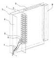
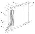
図1はこの発明の実施の形態1における光通信用パッケージの内部構造を示す斜視図であり、図2は図1に示す可動基板2をシェルフから引き出した状態を示す斜視図である。
【0018】
図1および図2に示すように、光通信用パッケージは、シェルフ(図示せず)と、メイン基板(プリント基板)1と、可動基板(可動部)2と、光コネクタ5とを備える。
【0019】
メイン基板1は、シェルフに収容され、コネクタ9で装置(シェルフ)と接続される。また、メイン基板1は、前方に前面パネル3を有する。
【0020】
可動基板2は、メイン基板1と隣り合う位置に設置され、図1に示す例ではメイン基板1と同等の大きさを有する。この可動基板2は、レール8を介してメイン基板1と接続され、メイン基板1に対してスライド可動にシェルフに収容される。
【0021】
上記可動基板2も、前面パネル4を有する。前面パネル4は、図1に示す例では、メイン基板1と可動基板2とをともにシェルフに収納した状態においてメイン基板1の前面パネル3と並んだ位置にあり、可動基板2から側方に立ち上がる壁部で構成され、光ファイバ7を導出するための開口を有する。
【0022】
上記の前面パネル4は、光コネクタ5と対向するように設けられ、光コネクタ5からの光がシェルフから外部へ放出されるのを遮る遮蔽部として機能する。したがって、前面パネル4の側方への突出高さは、図1に示す例では左右方向における光コネクタ5の積層高さ以上であることが好ましい。
【0023】
なお、光コネクタ5からの光がシェルフから外部へ放出されるのを抑制することができるものであれば、前面パネル4をはじめとする遮蔽部の形状や高さや数は任意に設定可能である。
【0024】
光コネクタ5は、可動基板2に複数取付けられ、この光コネクタ5に外部からの光コネクタ6が接続される。図1に示す例では、光コネクタ5は、可動基板2の側面から立ち上がる壁部に2列に取り付けられ、上下方向に多数配列されている。
【0025】
可動基板2は図2に示すように前後方向に摺動可能であるので、光コネクタ5は、可動基板2の可動方向に対し垂直方向に並ぶように配列されることとなる。それにより、多くの光コネクタ5を可動基板2に設置することができる。
【0026】
上記の構造を有する光通信用パッケージにおいて光コネクタ6を光コネクタ5に対し挿抜する際には、まず図2に示すように可動基板2を前方に引き出す。そしてこの状態で、光ファイバ7と接続される光コネクタ6を光コネクタ5に対し挿抜する。このとき、光コネクタ5から放出される光は前面パネル4で遮蔽され、この光は前面パネル4より外に出てくることはない。
【0027】
また、可動基板2のスライド方向と異なる直角方向(たとえば図1の上下方向や左右方向)に光コネクタ5を並べることにより、少ないスライド量でも多くの光コネクタ6を挿抜することができる。したがって、活線状態で多くの光コネクタ6を挿抜することが可能となる。
(実施の形態2)
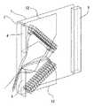
次に、図3と図4を用いて、本発明の実施の形態2について説明する。図3はこの発明の実施の形態2における光通信用パッケージの内部構造を示す斜視図であり、図4は図3に示す回転可動基板10をシェルフから引き出した状態を示す斜視図である。
【0028】
図3に示すように、本実施の形態2では、可動部を回転可動基板10で構成している。回転可動基板10は、メイン基板1と隣り合う位置に設置され、上端部に設けた回転軸を介してメイン基板1と接続され、この回転軸を中心として図4に示すようにメイン基板1に対し回動される。
【0029】
光コネクタ5は、図3および図4に示すように、回転可動基板10の側面に前面パネル4に対して斜め方向に並ぶように配列される。図3および図4に示す例では、光コネクタ5を保持する壁部の下端に向かうにつれて前面パネル4から離れるように壁部が前面パネル4に対して斜め方向に設けられている。そのため、実施の形態1よりも壁部の長さを長くすることができ、より多くの光コネクタ5を可動部に設置することができる。
【0030】
また、回転可動基板10の前面パネル4に、遮蔽板11を設けている。この遮蔽板11は前面パネル4と所定角度をなすように延在しており、光コネクタ5の一部と対向するように設けられる。
【0031】
本実施の形態では、該遮蔽板11と前面パネル4とが遮蔽部として機能し、これらにより光コネクタ5から放出される光が遮られ、シェルフより外に光が出てくることを阻止できる。
【0032】
上記以外の構成については、基本的に実施の形態1と同様であるので、重複説明は省略する。
【0033】
本実施の形態の光通信用パッケージにおいて光コネクタ6を光コネクタ5に対し挿抜する際には、まず図4に示すように回転可動基板10を回転させて前方に引き出し、この状態で光コネクタ6を光コネクタ5に対し挿抜する。
【0034】
このとき、上記のように回転可動基板10と前面パネル4とで光コネクタ5から放出される光がシェルフより外に出てくることを阻止でき、また光コネクタ5を保持する壁部と前面パネル4とのなす角度を適切に調節することで、図4に示すように回転可動基板10を回転させて本体から引き出した際に、光コネクタ5がパッケージ前面に並ぶようにすることができる。それにより、光ファイバ7の脱着を容易に行える。
(実施の形態3)
次に、図5と図6を用いて、本発明の実施の形態3について説明する。図5はこの発明の実施の形態3における光通信用パッケージの内部構造を示す斜視図であり、図6は図5に示す回転可動基板12をシェルフから引き出した状態を示す斜視図である。
【0035】
図5と図6に示すように、本実施の形態では2つの回転可動基板12,13を設けている。このように複数の回転可動基板12,13を設けることにより、実施の形態2よりもさらに多くの光コネクタ5を設置することができる。各回転可動基板12,13は、実施の形態2の場合と同様に回転軸を介してメイン基板1と接続され、この回転軸を中心として図6に示すようにメイン基板1に対しそれぞれ回動される。
【0036】
各回転可動基板12,13に設置される光コネクタ5は、実施の形態2の場合と同様に、前面パネル4に対しそれぞれ斜め方向に並ぶように配列される。
【0037】
本実施の形態の光通信用パッケージにおいて光コネクタ6を光コネクタ5に対し挿抜する際には、まず図6に示すように一方の回転可動基板12を回転させて前方に引き出し、この状態で光コネクタ6を光コネクタ5に対し挿抜する。このとき光コネクタ5はパッケージ前面に整列している。光コネクタ6の挿抜が完了して一方の回転可動基板12をシェルフに収納した後、別の回転可動基板13を動かして同様に光コネクタ6の挿抜を行う。
【0038】
なお、本実施の形態3では、2つの回転可動基板12,13を設ける場合について説明したが、回転可動基板12,13の数は複数であれば任意に設定可能である。
【0039】
また、複数の回転可動基板12,13を回動操作して引き出す時に、基板同士あるいは基板と光コネクタとが接触しないように回転可動基板12,13に接触回避用の切欠を設けたり、光コネクタの設置位置をずらせる等の工夫を施すことが好ましい。さらに、図5,6では示していないが、前面パネル4に実施の形態2と同様の遮蔽板11を設けてもよい。
【0040】
以上のように本発明の実施の形態について説明を行なったが、各実施の形態の特徴的構成を適宜組み合わせてもよい。また、今回開示した実施の形態はすべての点で例示であって制限的なものではないと考えられるべきである。本発明の範囲は特許請求の範囲によって示され、特許請求の範囲と均等の意味および範囲内でのすべての変更が含まれる。
【0041】
【発明の効果】
この発明に係る光通信用パッケージによれば、可動基板の引出し方向と垂直方向に光コネクタを複数装備することにより、より多くの光コネクタを装備することができ、なおかつ光コネクタの挿抜時に可動部の移動距離を少なくすることができるので活線状態において光コネクタの挿抜を行うことができる。また、遮蔽部により、光コネクタ抜去時に放出される光をシェルフより外に出ないようにすることができ、該抜去時に光が目などに入るのを阻止することができる。
【0042】
可動基板を回転可動とした場合には、より多くの光コネクタを装備することができ、該回転可動基板を複数設けることにより、さらに多くの光コネクタを装備することができる。
【図面の簡単な説明】
【図1】 この発明の実施の形態1を示す構成図である。
【図2】 この発明の実施の形態1の光コネクタ挿抜時の図である。
【図3】 この発明の実施の形態2を示す構成図である。
【図4】 この発明の実施の形態2の光コネクタ挿抜時の図である。
【図5】 この発明の実施の形態3を示す構成図である。
【図6】 この発明の実施の形態3の光コネクタ挿抜時の図である。
【図7】 従来の光通信用パッケージを示す構成図である。
【符号の説明】
1 メイン基板(プリント基板)、2 可動基板、3,4 前面パネル、5,6 光コネクタ、7 光ファイバ、8 レール、9 コネクタ、10,12,13 回転可動基板、11 遮蔽板、21 光通信装置、22 プリント基板、23 光入出力ケーブル、24 光コネクタ接続部、25 光コネクタ保持板、26 光コネクタ、31,32 支持具、33 光コネクタ移動板、34,35 長穴、37 基板固定板、38 摘まみネジ、39 固定具、41 ネジ穴。[0001]
BACKGROUND OF THE INVENTION
The present invention relates to an apparatus that performs communication using an optical fiber or the like, and relates to an apparatus in which a number of optical communication cables are installed in a communication package.
[0002]
[Prior art]
FIG. 7 shows an example of a conventional optical communication package disclosed in, for example, Japanese Patent Laid-Open No. 8-204358. In the figure, a plurality of
[0003]
On each substrate, an optical
[0004]
Each optical
[0005]
The operator can perform the work of inserting / removing the
[0006]
[Problems to be solved by the invention]
In such a conventional optical communication device, when the number of
[0007]
Furthermore, there is a possibility that light from the substrate may directly enter the eyes when the
[0008]
As a result, in the conventional optical communication apparatus as described above, it is difficult to insert and remove many
[0009]
The present invention has been made to solve the above-described problems, and is a light that can insert and remove many optical connectors in a live line state and can suppress light from being emitted from the optical communication package when the optical connector is removed. A communication package is obtained.
[0010]
[Means for Solving the Problems]
An optical communication package according to the present inventionis connected to a shelfby a connector and is placed at a position adjacent to the printed circuit board (main board) accommodated in the shelf,and is connected to the printed circuit board via a rail and pulled outto the shelf. A movable substrate that can be accommodated, a plurality of optical connectors attached to a wall that rises from a side surface of the movable substrate so as to be aligned in a direction perpendicular to a pulling direction of the movable substrate, and an optical connector that rises laterally from the movable substrate And a shielding portion that is provided to face each other and blocks light from the optical connector from being emitted from the shelf. The “shelf” is an optical communication device configured by one or a plurality of printed boards.
[0011]
By installing a plurality of optical connectors As thus arranged in the direction perpendicular tothe drawing direction of the movablesubstrate, it is possible to shorten the movable distance of the movablesubstrate even when installed a large number of optical connectors, increasing the device Many optical connectors can be installed without doing so. Further, by providing the movablesubstrate with the shielding portion, it is possible to suppress the light from the optical connector from being emitted from the shelf.
[0012]
Yes kinematic substrate is accommodated in the shelf movable along the printed circuitboard. Here, “facing” is not limited to the case where the front faces each other so as to face each other, but for example, the
[0013]
A large number of optical connectors can be installed by arranging the optical connectors on the side surface of the movable substrate as described above. In particular, when the movable substrate has the same size as the printed substrate (main substrate), more optical connectors can be installed. Also, by providing a wall portion that rises on the movable substrate so as to face the optical connector, the light from the optical connector can be blocked by the wall portion, and the light is prevented from being emitted from the shelf to the outside. Can do.
[0014]
In another aspect, the optical communication package according to the present invention includes a rotatable movable substrate that is disposed at a position adjacent to the printed circuit board, is rotatably installed withrespect to the printed circuit board, and is connected to the printed circuit board via a rotation shaft. The shielding portion is provided so as to rise from the rotary movable substrate, and shields light from the optical connector from being emitted from the shelf. The optical connectors are arranged so as to be arranged in an oblique direction with respect to the shielding portion.
[0015]
As described above, a rotationally movable substrate may be provided as the movable part. At this time, it is possible to install more optical connectors by arranging the optical connectors so as to be arranged in an oblique direction with respect to the shielding portion. Further, by appropriately adjusting the installation position of the optical connector, the optical connector can be arranged in front of the package when the rotatable movable substrate is rotated and pulled out from the main body. Thereby, the optical fiber can be easily connected.
[0016]
A plurality of the rotary movable substrates may be provided. Thereby, more optical connectors can be installed. Further, for example, when inserting / removing an optical connector, only one rotatable movable substrate can be rotated to insert / remove the optical connector, and after storing one, another rotatable movable substrate can be moved to insert / remove the optical connector.
[0017]
DETAILED DESCRIPTION OF THE INVENTION
Hereinafter, embodiments of the present invention will be described with reference to FIGS.
(Embodiment 1)
FIG. 1 is a perspective view showing an internal structure of an optical communication package according to
[0018]
As shown in FIGS. 1 and 2, the optical communication package includes a shelf (not shown), a main board (printed board) 1, a movable board (movable part) 2, and an
[0019]
The
[0020]
The
[0021]
The
[0022]
The
[0023]
Note that the shape, height, and number of the shielding portions including the
[0024]
A plurality of
[0025]
Since the
[0026]
When the
[0027]
Further, by arranging the
(Embodiment 2)
Next,
[0028]
As shown in FIG. 3, in the second embodiment, the movable part is configured by a rotatable
[0029]
As shown in FIGS. 3 and 4, the
[0030]
A shielding
[0031]
In the present embodiment, the shielding
[0032]
Since the configuration other than the above is basically the same as that of the first embodiment, the redundant description is omitted.
[0033]
When the
[0034]
At this time, the light that is emitted from the
(Embodiment 3)
Next,
[0035]
As shown in FIGS. 5 and 6, in this embodiment, two rotary
[0036]
The
[0037]
When the
[0038]
In the third embodiment, the case where the two rotatable
[0039]
Further, when the plurality of rotary
[0040]
Although the embodiments of the present invention have been described above, the characteristic configurations of the embodiments may be appropriately combined. In addition, it should be considered that the embodiment disclosed this time is illustrative in all points and not restrictive. The scope of the present invention is defined by the terms of the claims, and includes meanings equivalent to the terms of the claims and all modifications within the scope.
[0041]
【The invention's effect】
According to the optical communication package of the present invention, bymounting a plurality of optical connectors in the direction perpendicular to thepulling-out direction of the movablesubstrate , more optical connectors can be mounted, and the movable part can be mounted when the optical connector is inserted or removed. Therefore, the optical connector can be inserted / removed in a live line state. Further, the shielding portion can prevent light emitted when the optical connector is removed from coming out of the shelf, and can prevent light from entering the eyes or the like when the optical connector is removed.
[0042]
When the movablesubstrate is rotationally movable, it is possible to equip more optical connectors, and by providing a plurality of the rotationally movablesubstrates , it is possible to equip more optical connectors.
[Brief description of the drawings]
FIG. 1 is a configuration diagram showing a first embodiment of the present invention.
FIG. 2 is a diagram when the optical connector according to
FIG. 3 is a block
FIG. 4 is a diagram when an optical connector according to
FIG. 5 is a block
FIG. 6 is a diagram when an optical connector according to
FIG. 7 is a block diagram showing a conventional optical communication package.
[Explanation of symbols]
DESCRIPTION OF
Claims (4)
Translated fromJapanese前記プリント基板と隣り合う位置に配置され、レールを介して前記プリント基板と接続され前記シェルフに引出し可能に収容される可動基板と、
前記可動基板の引出し方向に対し垂直方向に並ぶように前記可動基板の側面から立ち上がる壁部に取付けられた複数の光コネクタと、
前記可動基板から側方に立ち上がり前記光コネクタと対向するように設けられ、前記光コネクタからの光がシェルフから外へ放出されるのを遮る遮蔽部と、
を備えた光通信用パッケージ。A printed circuit boardconnected to the shelfby a connector and housed in the shelf;
A movable substrate that is disposed at a position adjacent to theprinted circuit board, is connected to the printed circuit board via a rail, and is housed in the shelf so as to be drawn out;
A plurality of optical connectors attached to a wall portion rising from a side surface of the movable substrate so as to be aligned in a direction perpendicular to a pulling direction of the movable substrate;
A shielding portion that is provided so as to rise from a side of the movable substrate and face the optical connector, and shields light from the optical connector from being emitted from the shelf;
Optical communication package with
前記プリント基板と隣り合う位置に配置され、前記プリント基板に対し回転可能に設置され、回転軸を介して前記プリント基板と接続された回転可動基板と、
前記回転可動基板の側面から立ち上がる壁部に取付けられた複数の光コネクタと、
前記回転可動基板から側方に立ち上がるように設けられ、前記光コネクタからの光がシェルフから外へ放出されるのを遮る遮蔽部とを備え、
前記光コネクタは、前記遮蔽部に対して斜め方向に並ぶように配列される、光通信用パッケージ。A printed circuit boardconnected to the shelfby a connector and housed in the shelf;
A rotationally movable substrate that is disposed at a position adjacent to the printed circuit board, is rotatably installed withrespect to the printed circuit board, and is connected to the printed circuit board via a rotation shaft ,
A plurality of optical connectors attached to the wall rising from the side surface of the rotatable movable substrate;
A shielding portion that is provided so as to rise sideways from the rotary movable substrate, and that blocks light from the optical connector from being emitted from the shelf;
The optical communication package is arranged so that the optical connectors are arranged in an oblique direction with respect to the shielding portion.
Priority Applications (1)
| Application Number | Priority Date | Filing Date | Title |
|---|---|---|---|
| JP2001369017AJP3964191B2 (en) | 2001-12-03 | 2001-12-03 | Optical communication package |
Applications Claiming Priority (1)
| Application Number | Priority Date | Filing Date | Title |
|---|---|---|---|
| JP2001369017AJP3964191B2 (en) | 2001-12-03 | 2001-12-03 | Optical communication package |
Publications (2)
| Publication Number | Publication Date |
|---|---|
| JP2003169026A JP2003169026A (en) | 2003-06-13 |
| JP3964191B2true JP3964191B2 (en) | 2007-08-22 |
Family
ID=19178493
Family Applications (1)
| Application Number | Title | Priority Date | Filing Date |
|---|---|---|---|
| JP2001369017AExpired - Fee RelatedJP3964191B2 (en) | 2001-12-03 | 2001-12-03 | Optical communication package |
Country Status (1)
| Country | Link |
|---|---|
| JP (1) | JP3964191B2 (en) |
Cited By (35)
| Publication number | Priority date | Publication date | Assignee | Title |
|---|---|---|---|---|
| US8184938B2 (en) | 2008-08-29 | 2012-05-22 | Corning Cable Systems Llc | Rear-installable fiber optic modules and equipment |
| US8280216B2 (en) | 2009-05-21 | 2012-10-02 | Corning Cable Systems Llc | Fiber optic equipment supporting moveable fiber optic equipment tray(s) and module(s), and related equipment and methods |
| US8433171B2 (en) | 2009-06-19 | 2013-04-30 | Corning Cable Systems Llc | High fiber optic cable packing density apparatus |
| US8452148B2 (en) | 2008-08-29 | 2013-05-28 | Corning Cable Systems Llc | Independently translatable modules and fiber optic equipment trays in fiber optic equipment |
| US8542973B2 (en) | 2010-04-23 | 2013-09-24 | Ccs Technology, Inc. | Fiber optic distribution device |
| US8593828B2 (en) | 2010-02-04 | 2013-11-26 | Corning Cable Systems Llc | Communications equipment housings, assemblies, and related alignment features and methods |
| US8625950B2 (en) | 2009-12-18 | 2014-01-07 | Corning Cable Systems Llc | Rotary locking apparatus for fiber optic equipment trays and related methods |
| US8660397B2 (en) | 2010-04-30 | 2014-02-25 | Corning Cable Systems Llc | Multi-layer module |
| US8662760B2 (en) | 2010-10-29 | 2014-03-04 | Corning Cable Systems Llc | Fiber optic connector employing optical fiber guide member |
| US8699838B2 (en) | 2009-05-14 | 2014-04-15 | Ccs Technology, Inc. | Fiber optic furcation module |
| US8705926B2 (en) | 2010-04-30 | 2014-04-22 | Corning Optical Communications LLC | Fiber optic housings having a removable top, and related components and methods |
| US8712206B2 (en) | 2009-06-19 | 2014-04-29 | Corning Cable Systems Llc | High-density fiber optic modules and module housings and related equipment |
| US8718436B2 (en) | 2010-08-30 | 2014-05-06 | Corning Cable Systems Llc | Methods, apparatuses for providing secure fiber optic connections |
| US8879881B2 (en) | 2010-04-30 | 2014-11-04 | Corning Cable Systems Llc | Rotatable routing guide and assembly |
| US8913866B2 (en) | 2010-03-26 | 2014-12-16 | Corning Cable Systems Llc | Movable adapter panel |
| US8953924B2 (en) | 2011-09-02 | 2015-02-10 | Corning Cable Systems Llc | Removable strain relief brackets for securing fiber optic cables and/or optical fibers to fiber optic equipment, and related assemblies and methods |
| US8989547B2 (en) | 2011-06-30 | 2015-03-24 | Corning Cable Systems Llc | Fiber optic equipment assemblies employing non-U-width-sized housings and related methods |
| US8985862B2 (en) | 2013-02-28 | 2015-03-24 | Corning Cable Systems Llc | High-density multi-fiber adapter housings |
| US8995812B2 (en) | 2012-10-26 | 2015-03-31 | Ccs Technology, Inc. | Fiber optic management unit and fiber optic distribution device |
| US9008485B2 (en) | 2011-05-09 | 2015-04-14 | Corning Cable Systems Llc | Attachment mechanisms employed to attach a rear housing section to a fiber optic housing, and related assemblies and methods |
| US9020320B2 (en) | 2008-08-29 | 2015-04-28 | Corning Cable Systems Llc | High density and bandwidth fiber optic apparatuses and related equipment and methods |
| US9022814B2 (en) | 2010-04-16 | 2015-05-05 | Ccs Technology, Inc. | Sealing and strain relief device for data cables |
| US9038832B2 (en) | 2011-11-30 | 2015-05-26 | Corning Cable Systems Llc | Adapter panel support assembly |
| US9059578B2 (en) | 2009-02-24 | 2015-06-16 | Ccs Technology, Inc. | Holding device for a cable or an assembly for use with a cable |
| US9075216B2 (en) | 2009-05-21 | 2015-07-07 | Corning Cable Systems Llc | Fiber optic housings configured to accommodate fiber optic modules/cassettes and fiber optic panels, and related components and methods |
| US9075217B2 (en) | 2010-04-30 | 2015-07-07 | Corning Cable Systems Llc | Apparatuses and related components and methods for expanding capacity of fiber optic housings |
| US9116324B2 (en) | 2010-10-29 | 2015-08-25 | Corning Cable Systems Llc | Stacked fiber optic modules and fiber optic equipment configured to support stacked fiber optic modules |
| US9213161B2 (en) | 2010-11-05 | 2015-12-15 | Corning Cable Systems Llc | Fiber body holder and strain relief device |
| US9250409B2 (en) | 2012-07-02 | 2016-02-02 | Corning Cable Systems Llc | Fiber-optic-module trays and drawers for fiber-optic equipment |
| US9279951B2 (en) | 2010-10-27 | 2016-03-08 | Corning Cable Systems Llc | Fiber optic module for limited space applications having a partially sealed module sub-assembly |
| US9519118B2 (en) | 2010-04-30 | 2016-12-13 | Corning Optical Communications LLC | Removable fiber management sections for fiber optic housings, and related components and methods |
| US9632270B2 (en) | 2010-04-30 | 2017-04-25 | Corning Optical Communications LLC | Fiber optic housings configured for tool-less assembly, and related components and methods |
| US9645317B2 (en) | 2011-02-02 | 2017-05-09 | Corning Optical Communications LLC | Optical backplane extension modules, and related assemblies suitable for establishing optical connections to information processing modules disposed in equipment racks |
| US9720195B2 (en) | 2010-04-30 | 2017-08-01 | Corning Optical Communications LLC | Apparatuses and related components and methods for attachment and release of fiber optic housings to and from an equipment rack |
| US11294135B2 (en) | 2008-08-29 | 2022-04-05 | Corning Optical Communications LLC | High density and bandwidth fiber optic apparatuses and related equipment and methods |
Families Citing this family (1)
| Publication number | Priority date | Publication date | Assignee | Title |
|---|---|---|---|---|
| US9042702B2 (en) | 2012-09-18 | 2015-05-26 | Corning Cable Systems Llc | Platforms and systems for fiber optic cable attachment |
- 2001
- 2001-12-03JPJP2001369017Apatent/JP3964191B2/ennot_activeExpired - Fee Related
Cited By (56)
| Publication number | Priority date | Publication date | Assignee | Title |
|---|---|---|---|---|
| US11294135B2 (en) | 2008-08-29 | 2022-04-05 | Corning Optical Communications LLC | High density and bandwidth fiber optic apparatuses and related equipment and methods |
| US11092767B2 (en) | 2008-08-29 | 2021-08-17 | Corning Optical Communications LLC | High density and bandwidth fiber optic apparatuses and related equipment and methods |
| US10094996B2 (en) | 2008-08-29 | 2018-10-09 | Corning Optical Communications, Llc | Independently translatable modules and fiber optic equipment trays in fiber optic equipment |
| US8452148B2 (en) | 2008-08-29 | 2013-05-28 | Corning Cable Systems Llc | Independently translatable modules and fiber optic equipment trays in fiber optic equipment |
| US10120153B2 (en) | 2008-08-29 | 2018-11-06 | Corning Optical Communications, Llc | Independently translatable modules and fiber optic equipment trays in fiber optic equipment |
| US10126514B2 (en) | 2008-08-29 | 2018-11-13 | Corning Optical Communications, Llc | Independently translatable modules and fiber optic equipment trays in fiber optic equipment |
| US10222570B2 (en) | 2008-08-29 | 2019-03-05 | Corning Optical Communications LLC | Independently translatable modules and fiber optic equipment trays in fiber optic equipment |
| US10416405B2 (en) | 2008-08-29 | 2019-09-17 | Corning Optical Communications LLC | Independently translatable modules and fiber optic equipment trays in fiber optic equipment |
| US12072545B2 (en) | 2008-08-29 | 2024-08-27 | Corning Optical Communications LLC | High density and bandwidth fiber optic apparatuses and related equipment and methods |
| US11754796B2 (en) | 2008-08-29 | 2023-09-12 | Corning Optical Communications LLC | Independently translatable modules and fiber optic equipment trays in fiber optic equipment |
| US10422971B2 (en) | 2008-08-29 | 2019-09-24 | Corning Optical Communicatinos LLC | High density and bandwidth fiber optic apparatuses and related equipment and methods |
| US11609396B2 (en) | 2008-08-29 | 2023-03-21 | Corning Optical Communications LLC | High density and bandwidth fiber optic apparatuses and related equipment and methods |
| US10444456B2 (en) | 2008-08-29 | 2019-10-15 | Corning Optical Communications LLC | High density and bandwidth fiber optic apparatuses and related equipment and methods |
| US11294136B2 (en) | 2008-08-29 | 2022-04-05 | Corning Optical Communications LLC | High density and bandwidth fiber optic apparatuses and related equipment and methods |
| US8184938B2 (en) | 2008-08-29 | 2012-05-22 | Corning Cable Systems Llc | Rear-installable fiber optic modules and equipment |
| US10459184B2 (en) | 2008-08-29 | 2019-10-29 | Corning Optical Communications LLC | High density and bandwidth fiber optic apparatuses and related equipment and methods |
| US10564378B2 (en) | 2008-08-29 | 2020-02-18 | Corning Optical Communications LLC | High density and bandwidth fiber optic apparatuses and related equipment and methods |
| US9910236B2 (en) | 2008-08-29 | 2018-03-06 | Corning Optical Communications LLC | High density and bandwidth fiber optic apparatuses and related equipment and methods |
| US11086089B2 (en) | 2008-08-29 | 2021-08-10 | Corning Optical Communications LLC | High density and bandwidth fiber optic apparatuses and related equipment and methods |
| US10852499B2 (en) | 2008-08-29 | 2020-12-01 | Corning Optical Communications LLC | High density and bandwidth fiber optic apparatuses and related equipment and methods |
| US9020320B2 (en) | 2008-08-29 | 2015-04-28 | Corning Cable Systems Llc | High density and bandwidth fiber optic apparatuses and related equipment and methods |
| US10606014B2 (en) | 2008-08-29 | 2020-03-31 | Corning Optical Communications LLC | Independently translatable modules and fiber optic equipment trays in fiber optic equipment |
| US9059578B2 (en) | 2009-02-24 | 2015-06-16 | Ccs Technology, Inc. | Holding device for a cable or an assembly for use with a cable |
| US8699838B2 (en) | 2009-05-14 | 2014-04-15 | Ccs Technology, Inc. | Fiber optic furcation module |
| US8538226B2 (en) | 2009-05-21 | 2013-09-17 | Corning Cable Systems Llc | Fiber optic equipment guides and rails configured with stopping position(s), and related equipment and methods |
| US8280216B2 (en) | 2009-05-21 | 2012-10-02 | Corning Cable Systems Llc | Fiber optic equipment supporting moveable fiber optic equipment tray(s) and module(s), and related equipment and methods |
| US9075216B2 (en) | 2009-05-21 | 2015-07-07 | Corning Cable Systems Llc | Fiber optic housings configured to accommodate fiber optic modules/cassettes and fiber optic panels, and related components and methods |
| US8712206B2 (en) | 2009-06-19 | 2014-04-29 | Corning Cable Systems Llc | High-density fiber optic modules and module housings and related equipment |
| US8433171B2 (en) | 2009-06-19 | 2013-04-30 | Corning Cable Systems Llc | High fiber optic cable packing density apparatus |
| US8625950B2 (en) | 2009-12-18 | 2014-01-07 | Corning Cable Systems Llc | Rotary locking apparatus for fiber optic equipment trays and related methods |
| US8992099B2 (en) | 2010-02-04 | 2015-03-31 | Corning Cable Systems Llc | Optical interface cards, assemblies, and related methods, suited for installation and use in antenna system equipment |
| US8593828B2 (en) | 2010-02-04 | 2013-11-26 | Corning Cable Systems Llc | Communications equipment housings, assemblies, and related alignment features and methods |
| US8913866B2 (en) | 2010-03-26 | 2014-12-16 | Corning Cable Systems Llc | Movable adapter panel |
| US9022814B2 (en) | 2010-04-16 | 2015-05-05 | Ccs Technology, Inc. | Sealing and strain relief device for data cables |
| US8542973B2 (en) | 2010-04-23 | 2013-09-24 | Ccs Technology, Inc. | Fiber optic distribution device |
| US8879881B2 (en) | 2010-04-30 | 2014-11-04 | Corning Cable Systems Llc | Rotatable routing guide and assembly |
| US9075217B2 (en) | 2010-04-30 | 2015-07-07 | Corning Cable Systems Llc | Apparatuses and related components and methods for expanding capacity of fiber optic housings |
| US8705926B2 (en) | 2010-04-30 | 2014-04-22 | Corning Optical Communications LLC | Fiber optic housings having a removable top, and related components and methods |
| US9632270B2 (en) | 2010-04-30 | 2017-04-25 | Corning Optical Communications LLC | Fiber optic housings configured for tool-less assembly, and related components and methods |
| US9519118B2 (en) | 2010-04-30 | 2016-12-13 | Corning Optical Communications LLC | Removable fiber management sections for fiber optic housings, and related components and methods |
| US8660397B2 (en) | 2010-04-30 | 2014-02-25 | Corning Cable Systems Llc | Multi-layer module |
| US9720195B2 (en) | 2010-04-30 | 2017-08-01 | Corning Optical Communications LLC | Apparatuses and related components and methods for attachment and release of fiber optic housings to and from an equipment rack |
| US8718436B2 (en) | 2010-08-30 | 2014-05-06 | Corning Cable Systems Llc | Methods, apparatuses for providing secure fiber optic connections |
| US9279951B2 (en) | 2010-10-27 | 2016-03-08 | Corning Cable Systems Llc | Fiber optic module for limited space applications having a partially sealed module sub-assembly |
| US9116324B2 (en) | 2010-10-29 | 2015-08-25 | Corning Cable Systems Llc | Stacked fiber optic modules and fiber optic equipment configured to support stacked fiber optic modules |
| US8662760B2 (en) | 2010-10-29 | 2014-03-04 | Corning Cable Systems Llc | Fiber optic connector employing optical fiber guide member |
| US9213161B2 (en) | 2010-11-05 | 2015-12-15 | Corning Cable Systems Llc | Fiber body holder and strain relief device |
| US10481335B2 (en) | 2011-02-02 | 2019-11-19 | Corning Optical Communications, Llc | Dense shuttered fiber optic connectors and assemblies suitable for establishing optical connections for optical backplanes in equipment racks |
| US9645317B2 (en) | 2011-02-02 | 2017-05-09 | Corning Optical Communications LLC | Optical backplane extension modules, and related assemblies suitable for establishing optical connections to information processing modules disposed in equipment racks |
| US9008485B2 (en) | 2011-05-09 | 2015-04-14 | Corning Cable Systems Llc | Attachment mechanisms employed to attach a rear housing section to a fiber optic housing, and related assemblies and methods |
| US8989547B2 (en) | 2011-06-30 | 2015-03-24 | Corning Cable Systems Llc | Fiber optic equipment assemblies employing non-U-width-sized housings and related methods |
| US8953924B2 (en) | 2011-09-02 | 2015-02-10 | Corning Cable Systems Llc | Removable strain relief brackets for securing fiber optic cables and/or optical fibers to fiber optic equipment, and related assemblies and methods |
| US9038832B2 (en) | 2011-11-30 | 2015-05-26 | Corning Cable Systems Llc | Adapter panel support assembly |
| US9250409B2 (en) | 2012-07-02 | 2016-02-02 | Corning Cable Systems Llc | Fiber-optic-module trays and drawers for fiber-optic equipment |
| US8995812B2 (en) | 2012-10-26 | 2015-03-31 | Ccs Technology, Inc. | Fiber optic management unit and fiber optic distribution device |
| US8985862B2 (en) | 2013-02-28 | 2015-03-24 | Corning Cable Systems Llc | High-density multi-fiber adapter housings |
Also Published As
| Publication number | Publication date |
|---|---|
| JP2003169026A (en) | 2003-06-13 |
Similar Documents
| Publication | Publication Date | Title |
|---|---|---|
| JP3964191B2 (en) | Optical communication package | |
| JP4105696B2 (en) | Unit mounted on electronic device and transmission line connection mechanism of electronic device | |
| CN107437669B (en) | Cable backplane system with individually removable cable connector assemblies | |
| JP4855178B2 (en) | Plug-in unit mounting structure and electronic device | |
| US7489522B2 (en) | Case for electronic equipment and communication device | |
| US6698937B2 (en) | Optical connector mechanism | |
| CN104244655B (en) | Cable back board system | |
| CN104244661A (en) | Spacers for a cable backplane system | |
| TWI628995B (en) | Cable backplane system having mounting blocks | |
| TW201832420A (en) | Mechanism, methods, system and assembly of the same | |
| JP6100679B2 (en) | Optical wiring board and optical communication device using the same | |
| JPH08508364A (en) | Device for connecting circuit boards to terminal boards | |
| JP2643894B2 (en) | Communication device | |
| JP2783785B2 (en) | Pachinko machine frame structure | |
| KR20220075316A (en) | Storage units and information processing units | |
| JP2002136741A (en) | Attaching structure of game control board in pachinko game machine | |
| JP4217304B2 (en) | Shelf structure and electronic device using the shelf structure | |
| JP7634466B2 (en) | Media Converter | |
| US11888763B2 (en) | Systems, methods, and devices for replaceable elements within network switches | |
| JP2001102765A (en) | Electronic equipment cabinet | |
| JP3136244B2 (en) | Switchboard unit fixing device | |
| JP2003224373A (en) | Electronic device housing | |
| JP3974026B2 (en) | Cable surplus length processing equipment | |
| JPH0613774A (en) | Electronic device shelf structure | |
| JPH03148605A (en) | Housing structure of optical device |
Legal Events
| Date | Code | Title | Description |
|---|---|---|---|
| A621 | Written request for application examination | Free format text:JAPANESE INTERMEDIATE CODE: A621 Effective date:20040713 | |
| A977 | Report on retrieval | Free format text:JAPANESE INTERMEDIATE CODE: A971007 Effective date:20050912 | |
| A131 | Notification of reasons for refusal | Free format text:JAPANESE INTERMEDIATE CODE: A131 Effective date:20050927 | |
| A521 | Written amendment | Free format text:JAPANESE INTERMEDIATE CODE: A523 Effective date:20051125 | |
| A131 | Notification of reasons for refusal | Free format text:JAPANESE INTERMEDIATE CODE: A131 Effective date:20060725 | |
| A521 | Written amendment | Free format text:JAPANESE INTERMEDIATE CODE: A523 Effective date:20060919 | |
| TRDD | Decision of grant or rejection written | ||
| A01 | Written decision to grant a patent or to grant a registration (utility model) | Free format text:JAPANESE INTERMEDIATE CODE: A01 Effective date:20070515 | |
| A61 | First payment of annual fees (during grant procedure) | Free format text:JAPANESE INTERMEDIATE CODE: A61 Effective date:20070523 | |
| R150 | Certificate of patent or registration of utility model | Free format text:JAPANESE INTERMEDIATE CODE: R150 | |
| FPAY | Renewal fee payment (event date is renewal date of database) | Free format text:PAYMENT UNTIL: 20100601 Year of fee payment:3 | |
| FPAY | Renewal fee payment (event date is renewal date of database) | Free format text:PAYMENT UNTIL: 20110601 Year of fee payment:4 | |
| LAPS | Cancellation because of no payment of annual fees |