JP3960639B2 - Nonvolatile semiconductor memory device - Google Patents
Nonvolatile semiconductor memory deviceDownload PDFInfo
- Publication number
- JP3960639B2 JP3960639B2JP11648096AJP11648096AJP3960639B2JP 3960639 B2JP3960639 B2JP 3960639B2JP 11648096 AJP11648096 AJP 11648096AJP 11648096 AJP11648096 AJP 11648096AJP 3960639 B2JP3960639 B2JP 3960639B2
- Authority
- JP
- Japan
- Prior art keywords
- memory
- well
- source
- memory transistor
- erase block
- Prior art date
- Legal status (The legal status is an assumption and is not a legal conclusion. Google has not performed a legal analysis and makes no representation as to the accuracy of the status listed.)
- Expired - Lifetime
Links
- 239000004065semiconductorSubstances0.000titleclaimsdescription40
- 230000015654memoryEffects0.000claimsdescription161
- 238000002955isolationMethods0.000claimsdescription18
- 239000000758substrateSubstances0.000claimsdescription16
- 230000007547defectEffects0.000claimsdescription4
- 239000010410layerSubstances0.000description23
- LZIAMMQBHJIZAG-UHFFFAOYSA-N2-[di(propan-2-yl)amino]ethyl carbamimidothioateChemical compoundCC(C)N(C(C)C)CCSC(N)=NLZIAMMQBHJIZAG-UHFFFAOYSA-N0.000description14
- 238000010586diagramMethods0.000description10
- 230000006870functionEffects0.000description9
- 239000011229interlayerSubstances0.000description9
- 239000012535impuritySubstances0.000description6
- 238000000926separation methodMethods0.000description3
- 238000009792diffusion processMethods0.000description2
- 239000002184metalSubstances0.000description2
- 230000000903blocking effectEffects0.000description1
- 230000007423decreaseEffects0.000description1
- 230000000694effectsEffects0.000description1
- 230000005684electric fieldEffects0.000description1
- 238000000605extractionMethods0.000description1
- 230000007257malfunctionEffects0.000description1
- 230000002265preventionEffects0.000description1
- 230000000717retained effectEffects0.000description1
Images


Classifications
- H—ELECTRICITY
- H10—SEMICONDUCTOR DEVICES; ELECTRIC SOLID-STATE DEVICES NOT OTHERWISE PROVIDED FOR
- H10B—ELECTRONIC MEMORY DEVICES
- H10B69/00—Erasable-and-programmable ROM [EPROM] devices not provided for in groups H10B41/00 - H10B63/00, e.g. ultraviolet erasable-and-programmable ROM [UVEPROM] devices
- G—PHYSICS
- G11—INFORMATION STORAGE
- G11C—STATIC STORES
- G11C16/00—Erasable programmable read-only memories
- G11C16/02—Erasable programmable read-only memories electrically programmable
- G11C16/06—Auxiliary circuits, e.g. for writing into memory
- G11C16/10—Programming or data input circuits
- G11C16/14—Circuits for erasing electrically, e.g. erase voltage switching circuits
- G11C16/16—Circuits for erasing electrically, e.g. erase voltage switching circuits for erasing blocks, e.g. arrays, words, groups
Landscapes
- Non-Volatile Memory (AREA)
- Semiconductor Memories (AREA)
- Read Only Memory (AREA)
Description
Translated fromJapanese【0001】
【発明の属する技術分野】
この発明は、不揮発性半導体記憶装置に関し、特に、スタックゲート型メモリセル(メモリトランジスタ)を含む電気的にプログラムおよび消去可能な不揮発性半導体記憶装置(以下、「フラッシュメモリ」と称する)に関するものである。
【0002】
【従来の技術】
従来から、電気的にプログラムおよび消去可能な上記のフラッシュメモリは知られている。このフラッシュメモリはデータを記憶するための多数のメモリトランジスタを有している。図5には、従来のフラッシュメモリ内に形成される一般的なスタックゲート型メモリトランジスタ11の断面構造が示されている。
【0003】
図5を参照して、pウェル領域3の表面には間隔をあけてドレイン領域4とソース領域5とが形成されている。このドレイン領域4およびソース領域5は、この場合であれば高濃度のn型の不純物を含む。ドレイン領域4とソース領域5との間のpウェル領域3の表面上には、極めて薄い酸化膜などからなる絶縁膜(トンネル絶縁膜)7が約100Å程度の厚みに形成されている。このトンネル絶縁膜7の上にフローティングゲート8が形成され、このフローティングゲート8上に層間絶縁層9を介在してコントロールゲート(ワード線)10が形成されている。このように、メモリトランジスタ11は二重ゲート構造を有する。なお、上記のpウェル領域3は、p型半導体基板により置換えられるものであってもよい。
【0004】
上記のような構造を有するメモリトランジスタ11は、消去状態と呼ばれる状態あるいはプログラム状態と呼ばれる状態に保持される。ここで、フラッシュメモリの消去およびプログラムの一般的な定義について説明する。消去とは、複数のメモリトランジスタ11のしきい値電圧を一括して所定の状態に変えることをいい、プログラムとは、選択されたメモリトランジスタ11のしきい値電圧をもう1つの所定の状態に変えることをいう。具体的には、図5に示されるフローティングゲート8に電子が蓄積されているかあるいはフローティングゲート8から電子が放出されているかにより、上記の消去あるいはプログラムが行なわれる。
【0005】
上述のようなメモリトランジスタ11を有するフラッシュメモリの中でも、DINOR(DIvided bit-line NOR)型のフラッシュメモリと呼ばれるものが、IEICE TRANS. ELECTRON, VOL.E77-C, NO.8 AUGUST 1994, P.1279〜P.1285に開示されている。
【0006】
上記のDINOR型のフラッシュメモリでは、フローティングゲート8に電子が蓄積された状態が消去状態となり、フローティングゲート8から電子が引抜かれた状態がプログラム状態となる。
【0007】
図6には、DINOR型フラッシュメモリにおけるメモリトランジスタ11の消去状態あるいはプログラム状態が示されている。図6を参照して、消去状態すなわちフローティングゲート8に電子が注入されている状態では、コントロールゲート10から見たメモリトランジスタ11のしきい値電圧は相対的に高くなる。そのため、コントロールゲート電圧が、図6に示されるように、Vg1以上にならなければ、ドレイン4およびソース5間に所定値以上の電流(センス電流)は流れない。これは、フローティングゲート8に蓄積されている電子の負電荷によって正の電圧が打ち消されるからである。このような消去状態が図6における“1”に対応する。フローティングゲート8に蓄積された電子はそのままでは半永久的に消えないため、記憶されたデータも半永久的に保持される。
【0008】
一方、プログラム状態すなわちフローティングゲート8から電子が放出されている状態では、コントロールゲート10から見たメモリトランジスタ11のしきい値電圧は相対的に低くなる。この状態が図6における“0”に対応し、コントロールゲート電圧がVg0以上になることによりドレイン4およびソース5間に所定値以上の電流(センス電流)が流れる。
【0009】
上記のような2つの状態(消去状態あるいはプログラム状態)を検出することにより、メモリトランジスタ11に記憶されているデータを読取ることが可能となる。
【0010】
次に、図7(a),(b)を用いて、上記のDINOR型フラッシュメモリのプログラム動作および消去動作についてより詳しく説明する。
【0011】
まず図7(a)を参照して、プログラム動作時には、ドレイン4に書込電圧(正の高電圧)Vw(通常6V程度)を印加し、コントロールゲート10に負の高電圧−Vpp(−10V程度)を印加し、ソース5をオープン状態にする。それにより、ドレイン4とフローティングゲート8との重なった領域を介してFNトンネル現象によりフローティングゲート8からドレイン4へ電子が引抜かれる。その結果、メモリトランジスタ11のしきい値電圧が低下する。
【0012】
消去動作時には、図7(b)に示されるように、ドレイン4をフローティング状態にし、ソース5とpウェル領域3とに負の高電圧−Vppを印加し、コントロールゲート10に正の高電圧+Vppを印加する。それにより、トンネル絶縁膜7に高電界が印加され、トンネル現象によりpウェル領域3(半導体基板)からフローティングゲート8内に電子が注入される。その結果、メモリトランジスタ11のしきい値電圧が上昇する。
【0013】
【発明が解決しようとする課題】
上記のような電圧をメモリトランジスタ11に印加することによりメモリトランジスタ11が消去状態あるいはプログラム状態に移行され、データのプログラムや消去が行なわれる。しかしながら、上記のDINOR型フラッシュメモリの消去動作時には、次に説明するような問題点があった。その問題について図8および図9を用いて説明する。
【0014】
図8は、従来のDINOR型フラッシュメモリの消去動作に関与する回路を示すブロック図である。図8を参照して、半導体基板の主表面には複数のpウェル領域3aが形成され、このpウェル領域3aにはウェルドライバ60,ウェルデコーダ71およびウェル電源50が接続される。ウェルドライバ60はpウェル領域3aに所定の電圧を印加する機能を有し、ウェルデコーダ71は所定のpウェル領域3aを選択する機能を有し、ウェル電源50はpウェル領域3aに印加される所定の電圧を発生する機能を有する。
【0015】
1つのpウェル領域3a内には複数の消去ブロック26が配置される。この消去ブロック26は、複数個のメモリトランジスタ11により構成されるものであり、この消去ブロック26ごとに一括消去が行なわれる。そして、各消去ブロック26内のメモリトランジスタ11のソース5に接続されるソース線(図示せず)が形成され、このソース線はソース線ドライバ61に接続される。ソース線ドライバ61は、ソース線に所定の電位を印加する機能を有する。ソース線ドライバ61は、ブロックデコーダ70およびソース電源51に接続される。ブロックデコーダ70は、各pウェル領域3aに対応して設けられ、各pウェル領域3a内における所定の消去ブロック26を選択する機能を有する。ソース電源51は、ソース線に印加される所定の電圧を発生する機能を有する。
【0016】
上述のように、従来のフラッシュメモリにおいては、1つのpウェル領域3a内に複数の消去ブロック26が配置されていたため、消去動作時に、次に説明するような問題点が生じていた。その問題点について図9を用いて説明する。図9は、従来のフラッシュメモリの消去動作を説明するための概念図である。
【0017】
消去動作は各消去ブロック26ごとに行なわれるので、消去時には、図9に示されるように、同一のpウェル領域3a上には選択された消去ブロック26(選択消去ブロック)と、非選択の消去ブロック26(非選択消去ブロック)とが存在することとなる。
【0018】
そして、消去時には、pウェル領域3aに−Vppが印加される。また同時に、選択消去ブロック内のメモリトランジスタ11aのコントロールゲート10aには+Vppが印加され、メモリトランジスタ11aのドレイン4aはオープン状態とされ、メモリトランジスタ11aのソース5aには−Vppが印加される。一方、非選択消去ブロック内のメモリトランジスタ11bのコントロールゲートは接地され、メモリトランジスタ11bのドレイン4bはオープン状態とされ、メモリトランジスタ11bのソース5bには消去阻止電圧として−1/2Vppが印加される。
【0019】
ここで、非選択消去ブロック内のメモリトランジスタ11bと選択消去ブロック内のメモリトランジスタ11aとが同一のpウェル領域3a上に形成されているため、非選択消去ブロック内のメモリトランジスタ11bのソース5bに消去阻止電圧である−1/2Vppを印加したとしてもフローティングゲート8bから電子が引抜かれることを完全には阻止できない。言い換えれば、微量の電子がフローティングゲート8bから引抜かれる得る。
【0020】
そのため、同一のpウェル領域3a内に多数の消去ブロックが配置された場合あるいはデータの書換が多数回行なわれた場合には、誤消去される消去ブロック26が発生し得るものと考えられる。このような現象を、本明細書ではウェルディスターブと称することとする。このウェルディスターブは、フラッシュメモリの大容量化によりさらに厳しいものになると考えられる。
【0021】
この発明は、上記のような課題を解決するためになされたものである。この発明の目的は、消去動作時に発生するウェルディスターブを回避することが可能となる不揮発性半導体記憶装置を提供することにある。
【0022】
【課題を解決するための手段】
この発明に係る不揮発性半導体記憶装置は、フローティングゲート,ソースおよびドレインを含み半導体基板の主表面におけるメモリセルアレイ領域上に形成された複数のメモリトランジスタを有し、半導体基板からフローティングゲートに電子が注入されることにより消去動作が行なわれ、フローティングゲートから半導体基板内に電子が引抜かれることによりプログラム動作が行なわれるものであることを前提とする。そして、この発明に係る不揮発性半導体記憶装置は、第1と第2のウェル領域と、第1と第2の消去ブロックと、共通の電圧印加手段とを備える。第1と第2のウェル領域は、メモリセルアレイ領域内に間隔をあけて形成される。第1の消去ブロックは、第1のウェル領域上に形成された第1のメモリトランジスタ群により構成される。第2の消去ブロックは、第2のウェル領域上に形成された第2のメモリトランジスタ群により構成される。電圧印加手段は、第1と第2のウェル領域と接続され、かつ第1のメモリトランジスタ群のソースと第2のメモリトランジスタ群のソースとにスイッチ手段を介在して接続され、第1および第2のウェル領域と第1および第2のメモリトランジスタ群のソースとに所定の電圧を印加するためのものである。上記電圧印加手段は、半導体基板から選択された第1の消去ブロックの第1のメモリトランジスタ群のフローティングゲートに電子が注入され非選択の第2の消去ブロックの第2のメモリトランジスタ群のフローティングゲートに電子が注入されない場合に第1と第2のウェルに対して異なる電圧を印加する。
【0023】
上述のように、この発明に係る不揮発性半導体記憶装置では、各消去ブロックごとに独立したウェルが形成され、各々のウェルには共通の電圧印加手段が接続されている。それにより、消去動作時に、選択された消去ブロックが配置されるウェルと非選択の消去ブロックが配置されるウェルとに対しそれぞれ異なる電圧を印加することが可能となる。それにより、消去動作時に非選択の消去ブロックにおけるメモリトランジスタに対し上述のウェルディスターブがかかることを効果的に阻止することが可能となる。
【0024】
なお、上記の電圧印加手段は、第1および第2のウェル領域と第1および第2のメモリトランジスタ群のソースとに接続される共通のウェル/ソースドライバと、このウェル/ソースドライバに接続され第1または第2のウェル領域と第1または第2の消去ブロックとを選択するウェル/ブロックデコーダと、ウェル/ソースドライバに接続される共通のウェル/ソース電源とを含むものであることが好ましい。
【0025】
電圧印加手段を上記のような構成とすることにより、従来例と比べて回路構成を簡略化することが可能となる。以下にその理由について説明する。前述のように、各消去ブロックごとに独立したウェルを形成することにより、非選択の消去ブロック内のメモリトランジスタのソースに消去阻止電圧(−1/2Vpp)を印加する必要がなくなる。それにより、たとえば図8に示されるソース電源51をウェル電源50で代用することが可能となる。その結果、ソース電源51を省略することができる。また、1つのウェル領域に対して1つの消去ブロックが配置されるので、たとえば図8に示されるウェルデコーダ71をブロックデコーダ70で代用できる。それにより、図8に示されるウェルデコーダ71を省略することが可能となる。さらに、図8に示されるウェルドライバ71でソース線ドライバ61を代用できる。それにより、図8に示されるソース線ドライバ61を省略することが可能となる。以上のことより、不揮発性半導体記憶装置の回路構成を従来例よりも簡略化することが可能となる。そればかりでなく、上記の消去阻止電圧を使用しなくて済むので、制御も容易となる。
【0026】
また、メモリセルアレイ領域内には、さらに第3のウェル領域が形成され、この第3のウェル領域上には第1および第2の消去ブロックと同様の構成を有する欠陥救済のための冗長ブロックが形成されることが好ましい。
【0027】
上記のように、冗長ブロックが消去ブロックと同様の構成を有することにより、冗長ブロックに対しても、上記のウェルディスターブがかかるのを効果的に阻止できる。その結果、ウェルディスターブのかからない条件の下で消去ブロックと冗長ブロックとを置換えることが可能となる。
【0028】
また、第1と第2のウェル領域上には第1と第2のセレクトゲートトランジスタがそれぞれ形成され、第1と第2のメモリトランジスタ群の上方には該第1と第2のメモリトランジスタ群内における複数のメモリトランジスタのドレインと接続される第1と第2の副ビット線が絶縁層を介在してそれぞれ形成され、第1と第2の副ビット線の上方には絶縁層を介在して主ビット線が形成されることが好ましい。そして、主ビット線は、第1のセレクトゲートトランジスタを介して第1の副ビット線と接続され、第2のセレクトゲートトランジスタを介して第2の副ビット線と接続される。
【0029】
上記のように、第1と第2のセレクトゲートトランジスタがそれぞれ形成されることにより、この第1と第2のセレクトゲートトランジスタによって主ビット線と第1および第2の副ビット線との導通/遮断を制御することが可能となる。それにより、消去動作時における各消去ブロック内でのドレインディスターブを効果的に阻止することが可能となる。
【0030】
また、第1と第2のウェル領域を分離するとともにこの第1と第2のウェル領域をそれぞれ周囲からも分離するための分離領域が第1と第2のウェル領域の周囲に形成される。そして、第1と第2のメモリトランジスタ群の上方には、好ましくは、第1と第2のメモリトランジスタ群のソースと電気的に接続される第1と第2のソース線が絶縁層を介在してそれぞれ形成される。また、上記の分離領域上には、好ましくは、第1あるいは第2のソース線と接続され、第1あるいは第2のソース線の抵抗を低減するための補助ソース線が形成される。
【0031】
上記のように、第1と第2のウェル領域の周囲に分離領域を形成することにより、この分離領域の上に補助ソース線を形成することが可能となる。この補助ソース線は、第1あるいは第2のソース線のいずれかに接続される。このような補助ソース線を設けることにより、ソース線の抵抗を低減することが可能となる。
【0032】
また、第1のメモリトランジスタ群内の複数のメモリトランジスタは、この複数のメモリトランジスタのフローティングゲート上に絶縁層を介在して形成された第1のワード線を共有し、第1の消去ブロックは第1のワード線を共有するすべてのメモリトランジスタを含むように第1のワード線の全長に沿って配置されることが好ましい。また、第2のメモリトランジスタ群内の複数のメモリトランジスタは、この複数のメモリトランジスタのフローティングゲート上に絶縁層を介在して形成された第2のワード線を共有し、第2の消去ブロックは第2のワード線を共有するすべてのメモリトランジスタを含むように第2のワード線の全長に沿って配置されることが好ましい。
【0033】
上記のように、第1あるいは第2の消去ブロックが第1あるいは第2のワード線の全長に沿って配置されることにより、第1あるいは第2のワード線を共有するすべてのメモリトランジスタを第1の消去ブロックあるいは第2の消去ブロック内に含めることが可能となる。それにより、消去動作時に、第1あるいは第2のワード線により他の消去ブロックでディスターブが発生するのを効果的に阻止することが可能となる。
【0034】
【発明の実施の形態】
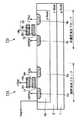
以下、この発明の実施の形態について図1〜図4を用いて説明する。図1は、この発明の1つの実施の形態におけるDINOR型フラッシュメモリの消去動作に関与する回路を示すブロック図である。
【0035】
図1を参照して、フラッシュメモリのメモリセルアレイ領域内には、複数のpウェル領域3が間隔をあけて形成されている。そして、各々のpウェル領域3内に消去ブロック26が1つずつ配置されている。各々のpウェル領域3は、電気的に分離されている。このように互いに分離されたpウェル領域3内に各消去ブロック26を配置することにより、消去動作時のウェルディスターブを効果的に阻止することが可能となる。
【0036】
各々のpウェル領域3は、ウェル/ソース線ドライバ60aに接続される。また、各消去ブロック26内に配置される複数のメモリトランジスタのソースに接続されるソース線が、スイッチ素子を介してウェル/ソース線ドライバ60aに接続される。したがって、このウェル/ソース線ドライバ60aは、図8に示されるソース線ドライバとしての機能をも併せ持つこととなる。それにより、図8に示されるソース線ドライバ61あるいはウェルドライバ60のいずれかを省略することが可能となる。
【0037】
ウェル/ソース線ドライバ60aは、ウェル/ソース電源50aおよびウェル/ブロックデコーダ70aに接続される。ウェル/ソース電源50aは、ウェル電源とソース電源としての機能を併せ持ち、pウェル領域3あるいは上記のソース線に印加する所定の電圧を発生する。ウェル/ブロックデコーダ70aは、各消去ブロック26あるいは各pウェル領域3を選択する機能を有するものである。
【0038】
以上のように、本発明では、図8に示される従来例と比較して回路構成を簡略化することが可能となる。
【0039】
また、図1に示される構成では、この図1に示される複数個の消去ブロック26のうちの1つを、そのまま欠陥救済のための冗長ブロックとして用いることができる。つまり、各消去ブロック26と冗長ブロックとを全く等価な構成とすることができる。それにより、ディスターブなどの諸特性が均一な条件の下で、各消去ブロック26と冗長ブロックとの置換えを行なうことが可能となる。
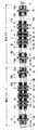
【0040】
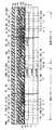
次に、図2および図3を用いて、本発明に係るフラッシュメモリの具体的な構造について詳しく説明する。図2は、この発明の1つの実施の形態におけるフラッシュメモリの部分平面図である。図3は、図2におけるIII−III線に沿う断面図である。
【0041】
図2および図3を参照して、p型半導体基板1の主表面にはnウェル領域2が形成される。このnウェル領域2はフラッシュメモリのメモリセルアレイ領域内に形成される。nウェル領域2の表面には間隔をあけてpウェル領域3が形成される。このpウェル領域3の周囲には分離酸化膜6が形成されている。この分離酸化膜6により、各々のpウェル領域3が分離される。なお、この分離酸化膜6の代わりに、分離用のトレンチを形成してもよい。それにより、分離幅を縮小することが可能となる。なお、上記のpウェル領域3は、通常の熱拡散により形成してもよいが、200keV以上の高エネルギで不純物を注入することにより形成してもよい。それにより、熱拡散によってpウェル領域3を形成する場合に比べ、pウェル領域3間の微細な分離が可能となる。
【0042】
pウェル領域3の表面にはセレクトゲートトランジスタが形成される。このセレクトゲートトランジスタは、セレクトゲート12と、n型不純物領域15a,15bを備える。そして、この場合であれば、pウェル領域3の両端に設けられる。この2つのセレクトゲートトランジスタ間には、1対の分離酸化膜6が形成され、この1対の分離酸化膜6間に複数のメモリトランジスタ11が形成される。
【0043】
メモリトランジスタ11は、1つの消去ブロック内に複数個配置され、メモリトランジスタ群を形成する。そして、このメモリトランジスタ群により1つの消去ブロックが構成される。メモリトランジスタ11の上方には、層間絶縁層13aを介在して副ビット線19a,19bが形成される。この副ビット線19a,19bは、コンタクトホール18を介して各メモリトランジスタ11のドレイン4と接続される。また、副ビット線19a,19bは、セレクトゲートトランジスタの一方のn型不純物領域15bともコンタクトホール17を介して接続される。
【0044】
副ビット線19a,19bを覆うように層間絶縁層13bが形成される。この層間絶縁層13b上には、たとえばAlを含む金属などからなる、配線層21,22,27,ソース線20および補助ソース線20aが形成される。配線層21はセレクトゲート12に接続され、ソース線20はメモリトランジスタ11のソース5に接続され、配線層22はメモリトランジスタ11のコントロールゲート(ワード線)10に接続される。なお、補助ソース線20aは、分離酸化膜6の上方に形成され、所定のソース線20に接続される。この補助ソース線20aを有することにより、ソース線20の抵抗を低減することが可能となる。
【0045】
上記の配線層21,22,27,ソース線20および補助ソース線20aを覆うように層間絶縁層13cが形成される。この層間絶縁層13c上には主ビット線24が形成される。この主ビット線24は、たとえばAlを含む金属などにより構成される。主ビット線24は、コンタクトホール23,配線層27およびコンタクトホール16を介してセレクトゲートトランジスタの他方のn型不純物領域15aに接続される。コンタクトホール16は層間絶縁層13a,13bを貫通して設けられ、その内部にはプラグ電極25が形成される。コンタクトホール23は、層間絶縁層13cを貫通して配線層27に到達するように設けられる。主ビット線24を覆うように絶縁層14が形成される。
【0046】
次に、上記のような構造を有する本発明に係るフラッシュメモリの消去動作について図4を用いて説明する。図4は、この発明に係るフラッシュメモリの消去動作を説明するための概念図である。
【0047】
図4を参照して、選択消去ブロック内のメモリトランジスタ11aの消去時に、非選択消去ブロック内のメモリトランジスタ11bにおけるコントロールゲート10bと,ソース5bと,ドレイン4bとメモリトランジスタ11bが形成されるpウェル領域3とにそれぞれ0Vが印加されている。このように、非選択消去ブロックが配置されるpウェル領域3の電位が0Vに固定されることにより、フラッシュメモリの消去動作時に、非選択消去ブロックにおけるウェルディスターブを阻止することが可能となる。なお、非選択消去ブロック内におけるメモリトランジスタ11bのコントロールゲート10b,ソース5b,ドレイン4bおよびpウェル領域3をオープン状態としてもよい。
【0048】
次に、再び図3を用いて、本発明に係るフラッシュメモリのさらなる特徴部分について説明する。上記のようにウェルディスターブを阻止できることに加えて、本発明に係るフラッシュメモリでは、消去動作時に、非選択消去ブロックにおけるドレインディスターブおよびワード線によるディスターブをも阻止することが可能となる。
【0049】
まずドレインディスターブについて説明する。図3に示されるように、主ビット線24は、セレクトゲートトランジスタを介在して副ビット線19aおよび19bと接続される。したがって、セレクトゲートトランジスタによって、主ビット線24と副ビット線19a,19bとの間の導通/遮断が制御される。それにより、このセレクトゲートトランジスタによって、非選択消去ブロックを主ビット線24に対して電気的に分離することが可能となる。それにより、消去動作時に、非選択消去ブロックにおけるドレインディスターブを阻止することが可能となる。
【0050】
また、図2に示されるように、コントロールゲート(ワード線)10は、主ビット線24と交差する方向に延在する。つまり、図1における消去ブロック26の長手方向と平行な方向にワード線が延在することとなる。このとき、ワード線の全長にわたって消去ブロック26が配置されることが好ましい。すなわち、1本のワード線を共有する複数個のメモリトランジスタをすべて1つの消去ブロック26内に含むように消去ブロック26が規定されることが好ましい。それにより、消去動作時に、非選択消去ブロック内におけるワード線によるディスターブを効果的に阻止することが可能となる。
【0051】
以上のように、この発明によれば、フラッシュメモリの消去動作時において、各消去ブロックをほぼ完全に電気的に分離することが可能となる。それにより、信頼性の高いフラッシュメモリが得られる。
【0052】
【発明の効果】
以上説明したように、この発明によれば、各消去ブロックごとに独立したウェルを形成するようにしたので、非選択消去ブロックにおける消去動作時のウェルディスターブを阻止することが可能となる。それにより、消去動作に起因する誤動作(誤消去)を効果的に阻止でき、信頼性の高い不揮発性半導体記憶装置が得られる。また、上記のように各消去ブロックごとにウェルを形成することにより、従来例よりも消去動作に関与する回路構成を簡略化することが可能となる。それにより、消去動作に関与する回路の占有面積を低減することが可能となる。さらに、セレクトゲートトランジスタを設け、かつワード線の全長にわたって消去ブロックを延在させることにより、消去動作時に、非選択消去ブロックにおけるドレインディスターブおよびワード線によるディスターブをも効果的に阻止することが可能となる。さらに、消去ブロックごとにウェルを形成することにより、消去ブロックと冗長ブロックとを全く等価な構成にすることが可能となる。それにより、ディスターブなどの諸特性がほぼ均一な条件の下で消去ブロックと冗長ブロックとの置換を行なうことが可能となる。さらに、各々の消去ブロックが形成されるウェル領域間を分離する分離領域を形成した場合には、この分離領域上の領域に補助ソース線を形成することが可能となる。それにより、ソース線の抵抗低減が可能となり、不揮発性半導体記憶装置の性能を向上させることも可能となる。
【図面の簡単な説明】
【図1】 この発明の1つの実施の形態におけるDINOR型フラッシュメモリの消去動作に関与する回路を示すブロック図である。
【図2】 この発明の1つの実施の形態におけるDINOR型フラッシュメモリの部分平面図である。
【図3】 図2におけるIII−III線に沿う断面図である。
【図4】 この発明に係るDINOR型フラッシュメモリの消去動作を説明するための概念図である。
【図5】 従来のフラッシュメモリにおける1つのメモリトランジスタを示す断面図である。
【図6】 従来のDINOR型フラッシュメモリの消去状態とプログラム状態とを示すグラフである。
【図7】 (a)は従来のDINOR型フラッシュメモリのプログラム動作を示す概念図である。
(b)は従来のDINOR型フラッシュメモリの消去動作を説明するための概念図である。
【図8】 従来のDINOR型フラッシュメモリの消去状態に関与する回路を示すブロック図である。
【図9】 従来のフラッシュメモリの消去動作を説明するための概念図である。
【符号の説明】
1 p型半導体基板、2 nウェル領域、3,3a pウェル領域、4a,4b,4 ドレイン、5a,5b,5 ソース、6 分離酸化膜、7a,7b,7トンネル絶縁膜、8a,8b,8 フローティングゲート、9a,9b,9,13a,13b,13c 層間絶縁層、10a,10b,10 コントロールゲート(ワード線)、11a,11b,11 メモリトランジスタ(メモリセル)、12 セレクトゲート、14 絶縁層、15a,15b n型不純物領域、16,17,18,23 コンタクトホール、19a,19b 副ビット線、20ソース線、20a 補助ソース線、21,22,27 配線層、24 主ビット線、25 プラグ電極、26 消去ブロック、50 ウェル電源、50a ウェル/ソース電源、51 ソース電源、60 ウェルドライバ、60a ウェル/ソース線ドライバ、61 ソース線ドライバ、70 ブロックデコーダ、70a ウェル/ブロックデコーダ、71 ウェルデコーダ。[0001]
BACKGROUND OF THE INVENTION
The present invention relates to a nonvolatile semiconductor memory device, and more particularly to an electrically programmable and erasable nonvolatile semiconductor memory device (hereinafter referred to as “flash memory”) including a stack gate type memory cell (memory transistor). is there.
[0002]
[Prior art]
Conventionally, the above-mentioned flash memory that can be electrically programmed and erased is known. This flash memory has a large number of memory transistors for storing data. FIG. 5 shows a cross-sectional structure of a general stack gate
[0003]
Referring to FIG. 5, a
[0004]
The
[0005]
Among flash memories having the
[0006]
In the DINOR type flash memory, the state in which electrons are accumulated in the
[0007]
FIG. 6 shows the erased state or programmed state of the
[0008]
On the other hand, in the programmed state, that is, in the state where electrons are emitted from the
[0009]
By detecting the two states (the erase state or the program state) as described above, the data stored in the
[0010]
Next, the program operation and erase operation of the DINOR type flash memory will be described in more detail with reference to FIGS.
[0011]
First, referring to FIG. 7A, during the program operation, a write voltage (positive high voltage) Vw (usually about 6V) is applied to the
[0012]
At the time of the erase operation, as shown in FIG. 7B, the
[0013]
[Problems to be solved by the invention]
By applying the voltage as described above to the
[0014]
FIG. 8 is a block diagram showing a circuit involved in the erase operation of a conventional DINOR type flash memory. Referring to FIG. 8, a plurality of
[0015]
A plurality of
[0016]
As described above, in the conventional flash memory, since a plurality of erase
[0017]
Since the erasing operation is performed for each erasing
[0018]
At the time of erasing, −Vpp is applied to
[0019]
Here, since the
[0020]
Therefore, when a large number of erase blocks are arranged in the same p-
[0021]
The present invention has been made to solve the above-described problems. An object of the present invention is to provide a nonvolatile semiconductor memory device capable of avoiding well disturb that occurs during an erase operation.
[0022]
[Means for Solving the Problems]
A nonvolatile semiconductor memory device according to the present invention includes a plurality of memory transistors formed on a memory cell array region on a main surface of a semiconductor substrate including a floating gate, a source and a drain, and electrons are injected from the semiconductor substrate to the floating gate. IsErase operation is performed., Electrons are extracted from the floating gate into the semiconductor substrateProgram operationIt is assumed that it is a thing. The nonvolatile semiconductor memory device according to the present invention includes first and second well regions, first and second erase blocks, and a common voltage applying unit. The first and second well regions are formed with a space in the memory cell array region. The first erase block is composed of a first memory transistor group formed on the first well region. The second erase block is composed of a second memory transistor group formed on the second well region. The voltage applying means is connected to the first and second well regions, and is connected to the source of the first memory transistor group and the source of the second memory transistor group via a switching means, and the first and second well regions are connected. A predetermined voltage is applied to the two well regions and the sources of the first and second memory transistor groups. The voltage applying means is from a semiconductor substrate.Of the first memory transistor group of the selected first erase block;Electrons are injected into the floating gateWhen electrons are not injected into the floating gate of the second memory transistor group of the non-selected second erase blockDifferent voltages are applied to the first and second wells.
[0023]
As described above, in the nonvolatile semiconductor memory device according to the present invention, an independent well is formed for each erase block, and a common voltage applying means is connected to each well. Thereby, during the erase operation, different voltages can be applied to the well in which the selected erase block is arranged and the well in which the non-selected erase block is arranged. As a result, it is possible to effectively prevent the above-described well disturb from being applied to the memory transistors in the non-selected erase block during the erase operation.
[0024]
The voltage applying means is connected to the common well / source driver connected to the first and second well regions and the sources of the first and second memory transistor groups, and to the well / source driver. It is preferable to include a well / block decoder for selecting the first or second well region and the first or second erase block, and a common well / source power source connected to the well / source driver.
[0025]
By configuring the voltage applying means as described above, the circuit configuration can be simplified as compared with the conventional example. The reason will be described below. As described above, by forming an independent well for each erase block, it is not necessary to apply the erase block voltage (−1/2 Vpp) to the source of the memory transistor in the non-selected erase block. Thereby, for example, the
[0026]
Further, a third well region is formed in the memory cell array region, and a redundant block for defect relief having the same configuration as the first and second erase blocks is formed on the third well region. Preferably it is formed.
[0027]
As described above, since the redundant block has the same configuration as that of the erase block, it is possible to effectively prevent the well disturb from being applied to the redundant block. As a result, it is possible to replace the erase block and the redundant block under conditions that are not disturbed.
[0028]
First and second select gate transistors are formed on the first and second well regions, respectively, and the first and second memory transistor groups are disposed above the first and second memory transistor groups. First and second subbit lines connected to the drains of the plurality of memory transistors are formed with an insulating layer interposed therebetween, and an insulating layer is interposed above the first and second subbit lines. The main bit line is preferably formed. The main bit line is connected to the first sub-bit line via the first select gate transistor, and is connected to the second sub-bit line via the second select gate transistor.
[0029]
As described above, since the first and second select gate transistors are formed, the first bit line and the first and second sub bit lines are connected to each other by the first and second select gate transistors. It becomes possible to control the interruption. Thereby, it is possible to effectively prevent drain disturbance in each erase block during the erase operation.
[0030]
Also, the first and second well regionsMinutesAnd the first and second well regions are separated from the surroundings.AlsoAn isolation region for separation is formed around the first and second well regions.TheThe first and second source lines electrically connected to the sources of the first and second memory transistor groups are preferably interposed above the first and second memory transistor groups with an insulating layer interposed therebetween. Are formed respectively. An auxiliary source line for reducing the resistance of the first or second source line is preferably formed on the isolation region. The auxiliary source line is connected to the first or second source line.
[0031]
As described above, by forming the isolation region around the first and second well regions, the auxiliary source line can be formed on the isolation region. The auxiliary source line is connected to either the first or second source line. By providing such an auxiliary source line, the resistance of the source line can be reduced.
[0032]
A plurality of memory transistors in the first memory transistor group share a first word line formed with an insulating layer on the floating gates of the plurality of memory transistors, and the first erase block is The first word line is preferably arranged along the entire length of the first word line so as to include all the memory transistors sharing the first word line. The plurality of memory transistors in the second memory transistor group share a second word line formed with an insulating layer on the floating gates of the plurality of memory transistors, and the second erase block is It is preferably arranged along the entire length of the second word line so as to include all the memory transistors sharing the second word line.
[0033]
As described above, the first or second erase block is arranged along the entire length of the first or second word line, so that all the memory transistors sharing the first or second word line are connected to the first or second word line. It can be included in one erase block or the second erase block. Accordingly, it is possible to effectively prevent the disturbance in other erase blocks due to the first or second word line during the erase operation.
[0034]
DETAILED DESCRIPTION OF THE INVENTION
Embodiments of the present invention will be described below with reference to FIGS. FIG. 1 is a block diagram showing a circuit involved in an erase operation of a DINOR type flash memory according to one embodiment of the present invention.
[0035]
Referring to FIG. 1, a plurality of p-
[0036]
Each p-
[0037]
Well /
[0038]
As described above, in the present invention, the circuit configuration can be simplified as compared with the conventional example shown in FIG.
[0039]
In the configuration shown in FIG. 1, one of the plurality of erase
[0040]
Next, the specific structure of the flash memory according to the present invention will be described in detail with reference to FIGS. FIG. 2 is a partial plan view of a flash memory according to one embodiment of the present invention. 3 is a cross-sectional view taken along line III-III in FIG.
[0041]
Referring to FIGS. 2 and 3,
[0042]
A select gate transistor is formed on the surface of
[0043]
A plurality of
[0044]
[0045]
An interlayer insulating
[0046]
Next, the erase operation of the flash memory according to the present invention having the above structure will be described with reference to FIG. FIG. 4 is a conceptual diagram for explaining the erase operation of the flash memory according to the present invention.
[0047]
Referring to FIG. 4, when erasing
[0048]
Next, further characteristic portions of the flash memory according to the present invention will be described with reference to FIG. 3 again. In addition to being able to prevent well disturb as described above, the flash memory according to the present invention can also prevent drain disturb and word line disturb in the unselected erase block during the erase operation.
[0049]
First, drain disturb will be described. As shown in FIG. 3,
[0050]
As shown in FIG. 2, the control gate (word line) 10 extends in a direction crossing the
[0051]
As described above, according to the present invention, each erase block can be electrically separated almost completely during the erase operation of the flash memory. Thereby, a highly reliable flash memory can be obtained.
[0052]
【The invention's effect】
As described above, according to the present invention, since an independent well is formed for each erase block, it is possible to prevent well disturb during an erase operation in a non-selected erase block. Thereby, a malfunction (erroneous erasure) due to the erase operation can be effectively prevented, and a highly reliable nonvolatile semiconductor memory device can be obtained. Further, by forming a well for each erase block as described above, it is possible to simplify the circuit configuration involved in the erase operation as compared with the conventional example. As a result, it is possible to reduce the area occupied by the circuits involved in the erase operation. Furthermore, by providing a select gate transistor and extending the erase block over the entire length of the word line, it is possible to effectively prevent drain disturb and word line disturb in the unselected erase block during the erase operation. Become. Further, by forming a well for each erase block, it is possible to make the erase block and the redundant block completely equivalent. As a result, it is possible to replace the erase block with the redundant block under conditions where characteristics such as disturb are substantially uniform. Further, when an isolation region for separating the well regions where the erase blocks are formed is formed, an auxiliary source line can be formed in the region on the isolation region. Thereby, the resistance of the source line can be reduced, and the performance of the nonvolatile semiconductor memory device can be improved.
[Brief description of the drawings]
FIG. 1 is a block diagram showing a circuit involved in an erase operation of a DINOR type flash memory according to an embodiment of the present invention.
FIG. 2 is a partial plan view of a DINOR type flash memory according to one embodiment of the present invention.
3 is a cross-sectional view taken along line III-III in FIG.
FIG. 4 is a conceptual diagram for explaining an erasing operation of the DINOR type flash memory according to the present invention.
FIG. 5 is a cross-sectional view showing one memory transistor in a conventional flash memory.
FIG. 6 is a graph showing an erase state and a program state of a conventional DINOR type flash memory.
FIG. 7A is a conceptual diagram showing a program operation of a conventional DINOR type flash memory.
(B) is a conceptual diagram for explaining an erasing operation of a conventional DINOR type flash memory.
FIG. 8 is a block diagram showing a circuit involved in an erase state of a conventional DINOR type flash memory.
FIG. 9 is a conceptual diagram for explaining an erase operation of a conventional flash memory.
[Explanation of symbols]
1 p-type semiconductor substrate, 2 n-well region, 3, 3a p-well region, 4a, 4b, 4 drain, 5a, 5b, 5 source, 6 isolation oxide film, 7a, 7b, 7 tunnel insulating film, 8a, 8b, 8 Floating gate, 9a, 9b, 9, 13a, 13b, 13c Interlayer insulating layer, 10a, 10b, 10 Control gate (word line), 11a, 11b, 11 Memory transistor (memory cell), 12 Select gate, 14 Insulating
Claims (11)
Translated fromJapanese前記メモリセルアレイ領域内に間隔をあけて形成された第1と第2のウェル領域と、
前記第1のウェル領域上に形成された第1のメモリトランジスタ群により構成される第1の消去ブロックと、
前記第2のウェル領域上に形成された第2のメモリトランジスタ群により構成される第2の消去ブロックと、
前記第1と第2のウェル領域と接続され、かつ前記第1のメモリトランジスタ群のソースと前記第2のメモリトランジスタ群のソースとにスイッチ手段を介在して接続され、前記第1および第2のウェル領域と前記第1および第2のメモリトランジスタ群のソースとに所定の電圧を印加するための共通の電圧印加手段とを備え、
前記第1と第2のウェル領域を分離するとともに前記第1と第2のウェル領域をそれぞれ周囲からも分離するための分離領域が前記第1と第2のウェル領域の周囲に形成され、
前記電圧印加手段は、前記半導体基板から選択された前記第1の消去ブロックの前記第1のメモリトランジスタ群の前記フローティングゲートに電子が注入され非選択の前記第2の消去ブロックの前記第2のメモリトランジスタ群の前記フローティングゲートに電子が注入されない場合に前記第1と第2のウェルに対して異なる電圧を印加することを特徴とする、不揮発性半導体記憶装置。A floating gate having a plurality of memory transistors formed in the memory cell array region in the main surface of the semiconductor substrate including a source and a drain, the electrons are injected from the semiconductor substrate into the floating gateerase operation by Rukoto is performedA nonvolatile semiconductor memory device in which aprogram operation is performed by extracting electrons from the floating gate into the semiconductor substrate,
First and second well regions formed at an interval in the memory cell array region;
A first erase block including a first memory transistor group formed on the first well region;
A second erase block including a second memory transistor group formed on the second well region;
Connected to the first and second well regions, and connected to the source of the first memory transistor group and the source of the second memory transistor group via a switching means, and the first and second well regions A common voltage applying means for applying a predetermined voltage to the well region and the sources of the first and second memory transistor groups,
An isolation region for isolating the first and second well regions and isolating the first and second well regions from their surroundings is formed around the first and second well regions,
The voltage applying means is configured such that electrons are injected into the floating gate ofthe first memory transistor group of the first erase block selected from the semiconductor substrate, andthe second erase block of the non-selected second erase block is selected. A nonvolatile semiconductor memory device, wherein different voltages are applied to the first and second wellswhen electrons are not injected into the floating gate of a memory transistor group .
前記第3のウェル領域上には、前記第1および第2の消去ブロックと同様の構成を有する欠陥救済のための冗長ブロックが形成される、請求項1に記載の不揮発性半導体記憶装置。A third well region is further formed in the memory cell array region,
2. The nonvolatile semiconductor memory device according to claim 1, wherein a redundancy block for defect relief having a configuration similar to that of the first and second erase blocks is formed on the third well region.
前記第1と第2のメモリトランジスタ群の上方には該第1と第2のメモリトランジスタ群内における複数の前記メモリトランジスタのドレインと接続される第1と第2の副ビット線が絶縁層を介在してそれぞれ形成され、
前記第1と第2の副ビット線の上方には絶縁層を介在して主ビット線が形成され、
前記主ビット線は、前記第1のセレクトゲートトランジスタを介して前記第1の副ビット線と接続され、前記第2のセレクトゲートトランジスタを介して前記第2の副ビット線と接続される、請求項1に記載の不揮発性半導体記憶装置。First and second select gate transistors are formed on the first and second well regions,
Above the first and second memory transistor groups, first and second subbit lines connected to the drains of the plurality of memory transistors in the first and second memory transistor groups have an insulating layer. Each formed with intervening,
A main bit line is formed above the first and second sub bit lines with an insulating layer interposed therebetween,
The main bit line is connected to the first sub-bit line via the first select gate transistor, and is connected to the second sub-bit line via the second select gate transistor. Item 12. The nonvolatile semiconductor memory device according to Item 1.
前記分離領域上には、前記第1あるいは第2のソース線と接続され該第1あるいは第2のソース線の抵抗を低減するための補助ソース線が形成される、請求項1に記載の不揮発性半導体記憶装置。Above the first and second memory transistor groups, there are first and second source lines electrically connected to the sources of the first and second memory transistor groups with an insulating layer interposed therebetween, respectively. Formed,
2. The nonvolatile source according to claim 1, wherein an auxiliary source line connected to the first or second source line for reducing resistance of the first or second source line is formed on the isolation region. Semiconductor memory device.
前記第1の消去ブロックは、前記第1のワード線を共有するすべての前記メモリトランジスタを含むように前記第1のワード線の全長に沿って配置され、
前記第2のメモリトランジスタ群内の複数の前記メモリトランジスタは、該複数のメモリトランジスタの前記フローティングゲート上に絶縁層を介在して形成された第2のワード線を共有し、
前記第2の消去ブロックは、前記第2のワード線を共有するすべての前記メモリトランジスタを含むように前記第2のワード線の全長に沿って配置される、請求項1に記載の不揮発性半導体記憶装置。The plurality of memory transistors in the first memory transistor group share a first word line formed through an insulating layer on the floating gates of the plurality of memory transistors,
The first erase block is disposed along the entire length of the first word line so as to include all the memory transistors sharing the first word line;
The plurality of memory transistors in the second memory transistor group share a second word line formed on the floating gates of the plurality of memory transistors with an insulating layer interposed therebetween,
2. The nonvolatile semiconductor device according to claim 1, wherein the second erase block is arranged along the entire length of the second word line so as to include all the memory transistors sharing the second word line. Storage device.
前記メモリセルアレイ領域内に間隔をあけて形成された第1と第2のウェル領域と、
前記第1のウェル領域上に形成された第1のメモリトランジスタ群により構成される第1の消去ブロックと、
前記第2のウェル領域上に形成された第2のメモリトランジスタ群により構成される第2の消去ブロックと、
前記第1と第2のウェル領域と接続され、かつ前記第1のメモリトランジスタ群のソースと前記第2のメモリトランジスタ群のソースとにスイッチ手段を介在して接続され、前記半導体基板から選択された前記第1の消去ブロックの前記第1のメモリトランジスタ群の前記フローティングゲートに電子が注入され非選択の前記第2の消去ブロックの前記第2のメモリトランジスタ群の前記フローティングゲートに電子が注入されない場合に前記第1および第2のウェル領域に対して異なる電圧を印加可能であり、前記第1および第2のメモリトランジスタ群のソースに所定の電圧を印加可能な共通の電圧印加手段とを備え、
前記第1と第2のウェル領域を分離するとともに前記第1と第2のウェル領域をそれぞれ周囲からも分離するための分離領域が前記第1と第2のウェル領域の周囲に形成され、
前記第1と第2のメモリトランジスタ群の上方には、前記第1と第2のメモリトランジスタ群のソースと電気的に接続される第1と第2のソース線が絶縁層を介在してそれぞれ形成され、
前記分離領域上には、前記第1あるいは第2のソース線と接続され該第1あるいは第2のソース線の抵抗を低減するための補助ソース線が形成される、不揮発性半導体記憶装置。A floating gate having a plurality of memory transistors formed in the memory cell array region in the main surface of the semiconductor substrate including a source and a drain, the electrons are injected from the semiconductor substrate into the floating gateerase operation by Rukoto is performedA nonvolatile semiconductor memory device in which aprogram operation is performed by extracting electrons from the floating gate into the semiconductor substrate,
First and second well regions formed at an interval in the memory cell array region;
A first erase block including a first memory transistor group formed on the first well region;
A second erase block including a second memory transistor group formed on the second well region;
Connected to the first and second well regions and connected to the source of the first memory transistor group and the source of the second memory transistor group via a switching means, andselected from the semiconductor substrateIn addition , electrons are injected into the floating gate ofthe first memory transistor group of the first erase block, and electrons are not injected into the floating gate ofthe second memory transistor group of the non-selected second erase block. If the it is possible applying different voltages to the first and second well regions, and a common voltage applying means capable of applying a predetermined voltage to the source of the first and second memory transistors ,
An isolation region for isolating the first and second well regions and isolating the first and second well regions from their surroundings is formed around the first and second well regions,
Above the first and second memory transistor groups, there are first and second source lines electrically connected to the sources of the first and second memory transistor groups with an insulating layer interposed therebetween, respectively. Formed,
A non-volatile semiconductor memory device, wherein an auxiliary source line for reducing the resistance of the first or second source line connected to the first or second source line is formed on the isolation region.
前記第3のウェル領域上には、前記第1および第2の消去ブロックと同様の構成を有する欠陥救済のための冗長ブロックが形成される、請求項7に記載の不揮発性半導体記憶装置。A third well region is further formed in the memory cell array region,
The nonvolatile semiconductor memory device according to claim 7, wherein a redundancy block for defect relief having a configuration similar to that of the first and second erase blocks is formed on the third well region.
前記第1と第2のメモリトランジスタ群の上方には該第1と第2のメモリトランジスタ群内における複数の前記メモリトランジスタのドレインと接続される第1と第2の副ビット線が絶縁層を介在してそれぞれ形成され、
前記第1と第2の副ビット線の上方には絶縁層を介在して主ビット線が形成され、
前記主ビット線は、前記第1のセレクトゲートトランジスタを介して前記第1の副ビット線と接続され、前記第2のセレクトゲートトランジスタを介して前記第2の副ビット線と接続される、請求項7に記載の不揮発性半導体記憶装置。First and second select gate transistors are formed on the first and second well regions,
Above the first and second memory transistor groups, first and second subbit lines connected to the drains of the plurality of memory transistors in the first and second memory transistor groups have an insulating layer. Each formed with intervening,
A main bit line is formed above the first and second sub bit lines with an insulating layer interposed therebetween,
The main bit line is connected to the first sub-bit line via the first select gate transistor, and is connected to the second sub-bit line via the second select gate transistor. Item 8. The nonvolatile semiconductor memory device according to Item 7.
前記第1の消去ブロックは、前記第1のワード線を共有するすべての前記メモリトランジスタを含むように前記第1のワード線の全長に沿って配置され、
前記第2のメモリトランジスタ群内の複数の前記メモリトランジスタは、該複数のメモリトランジスタの前記フローティングゲート上に絶縁層を介在して形成された第2のワード線を共有し、
前記第2の消去ブロックは、前記第2のワード線を共有するすべての前記メモリトランジスタを含むように前記第2のワード線の全長に沿って配置される、請求項7に記載の不揮発性半導体記憶装置。The plurality of memory transistors in the first memory transistor group share a first word line formed through an insulating layer on the floating gates of the plurality of memory transistors,
The first erase block is disposed along the entire length of the first word line so as to include all the memory transistors sharing the first word line;
The plurality of memory transistors in the second memory transistor group share a second word line formed on the floating gates of the plurality of memory transistors with an insulating layer interposed therebetween,
The nonvolatile semiconductor according to claim 7, wherein the second erase block is arranged along the entire length of the second word line so as to include all the memory transistors sharing the second word line. Storage device.
Priority Applications (4)
| Application Number | Priority Date | Filing Date | Title |
|---|---|---|---|
| JP11648096AJP3960639B2 (en) | 1996-05-10 | 1996-05-10 | Nonvolatile semiconductor memory device |
| KR1019970017492AKR100244406B1 (en) | 1996-05-10 | 1997-05-07 | Non-volatile semiconductor memory device |
| US08/852,817US5994732A (en) | 1996-05-10 | 1997-05-07 | Nonvolatile semiconductor memory device |
| TW086106138ATW359900B (en) | 1996-05-10 | 1997-05-08 | Nonvolatile semiconductor storage |
Applications Claiming Priority (1)
| Application Number | Priority Date | Filing Date | Title |
|---|---|---|---|
| JP11648096AJP3960639B2 (en) | 1996-05-10 | 1996-05-10 | Nonvolatile semiconductor memory device |
Publications (2)
| Publication Number | Publication Date |
|---|---|
| JPH09307005A JPH09307005A (en) | 1997-11-28 |
| JP3960639B2true JP3960639B2 (en) | 2007-08-15 |
Family
ID=14688159
Family Applications (1)
| Application Number | Title | Priority Date | Filing Date |
|---|---|---|---|
| JP11648096AExpired - LifetimeJP3960639B2 (en) | 1996-05-10 | 1996-05-10 | Nonvolatile semiconductor memory device |
Country Status (4)
| Country | Link |
|---|---|
| US (1) | US5994732A (en) |
| JP (1) | JP3960639B2 (en) |
| KR (1) | KR100244406B1 (en) |
| TW (1) | TW359900B (en) |
Families Citing this family (21)
| Publication number | Priority date | Publication date | Assignee | Title |
|---|---|---|---|---|
| JP3898305B2 (en)* | 1997-10-31 | 2007-03-28 | 富士通株式会社 | Semiconductor storage device, control device and control method for semiconductor storage device |
| US6147903A (en) | 1997-12-12 | 2000-11-14 | Matsushita Electronics Corporation | Non-volatile semiconductor memory device and method for driving the same |
| JP4434405B2 (en) | 2000-01-27 | 2010-03-17 | 株式会社ルネサステクノロジ | Nonvolatile semiconductor memory device |
| EP1178491A1 (en)* | 2000-08-02 | 2002-02-06 | STMicroelectronics S.r.l. | A semiconductor memory |
| DE10038877A1 (en)* | 2000-08-09 | 2002-02-28 | Infineon Technologies Ag | Memory cell and manufacturing process |
| US6438030B1 (en)* | 2000-08-15 | 2002-08-20 | Motorola, Inc. | Non-volatile memory, method of manufacture, and method of programming |
| AU2002227107A1 (en)* | 2000-10-30 | 2002-05-15 | Virtual Silicon Technology, Inc. | Common source eeprom and flash memory |
| JP3963420B2 (en) | 2000-11-15 | 2007-08-22 | 株式会社東芝 | Semiconductor memory device |
| FR2816751A1 (en)* | 2000-11-15 | 2002-05-17 | St Microelectronics Sa | Flash memory erasable by page and method for data storaage, comprising array with counter and sectors, and circuits for reading page address and incrementing counter |
| US6545310B2 (en)* | 2001-04-30 | 2003-04-08 | Motorola, Inc. | Non-volatile memory with a serial transistor structure with isolated well and method of operation |
| KR20020089587A (en)* | 2001-05-23 | 2002-11-30 | 삼성전자 주식회사 | non-volatile semiconductor memory devices having sector structure formed with common bulk |
| US6844588B2 (en)* | 2001-12-19 | 2005-01-18 | Freescale Semiconductor, Inc. | Non-volatile memory |
| US6876582B2 (en)* | 2002-05-24 | 2005-04-05 | Hynix Semiconductor, Inc. | Flash memory cell erase scheme using both source and channel regions |
| JP4642018B2 (en)* | 2004-04-21 | 2011-03-02 | スパンション エルエルシー | NONVOLATILE SEMICONDUCTOR DEVICE AND AUTOMATIC REMEDY METHOD FOR ERASE OPERATION OF NONVOLATILE SEMICONDUCTOR DEVICE |
| US20070140008A1 (en)* | 2005-12-21 | 2007-06-21 | Microchip Technology Incorporated | Independently programmable memory segments within an NMOS electrically erasable programmable read only memory array achieved by P-well separation and method therefor |
| US7606076B2 (en)* | 2007-04-05 | 2009-10-20 | Sandisk Corporation | Sensing in non-volatile storage using pulldown to regulated source voltage to remove system noise |
| US7447079B2 (en)* | 2007-04-05 | 2008-11-04 | Sandisk Corporation | Method for sensing negative threshold voltages in non-volatile storage using current sensing |
| JP5072696B2 (en)* | 2008-04-23 | 2012-11-14 | 株式会社東芝 | Three-dimensional stacked nonvolatile semiconductor memory |
| US8378422B2 (en)* | 2009-02-06 | 2013-02-19 | Taiwan Semiconductor Manufacturing Company, Ltd. | Electrostatic discharge protection device comprising a plurality of highly doped areas within a well |
| JP5466729B2 (en)* | 2012-06-01 | 2014-04-09 | ルネサスエレクトロニクス株式会社 | Nonvolatile semiconductor memory device |
| US9308351B2 (en)* | 2013-05-28 | 2016-04-12 | Smh Device Corp. | Tunneled catheter with hemostasis mechanism |
Family Cites Families (6)
| Publication number | Priority date | Publication date | Assignee | Title |
|---|---|---|---|---|
| JPS63211767A (en)* | 1987-02-27 | 1988-09-02 | Toshiba Corp | semiconductor storage device |
| JPH0324762A (en)* | 1989-06-22 | 1991-02-01 | Hitachi Ltd | Semiconductor integrated circuit device |
| JPH03290960A (en)* | 1990-03-30 | 1991-12-20 | Toshiba Corp | Non-volatile semiconductor memory device |
| JP2655765B2 (en)* | 1991-05-29 | 1997-09-24 | ローム株式会社 | Semiconductor device |
| JPH07161845A (en)* | 1993-12-02 | 1995-06-23 | Nec Corp | Semiconductor nonvolatile memory |
| JPH07235650A (en)* | 1993-12-27 | 1995-09-05 | Mitsubishi Electric Corp | Nonvolatile semiconductor memory device |
- 1996
- 1996-05-10JPJP11648096Apatent/JP3960639B2/ennot_activeExpired - Lifetime
- 1997
- 1997-05-07USUS08/852,817patent/US5994732A/ennot_activeExpired - Lifetime
- 1997-05-07KRKR1019970017492Apatent/KR100244406B1/ennot_activeExpired - Fee Related
- 1997-05-08TWTW086106138Apatent/TW359900B/ennot_activeIP Right Cessation
Also Published As
| Publication number | Publication date |
|---|---|
| JPH09307005A (en) | 1997-11-28 |
| US5994732A (en) | 1999-11-30 |
| KR970077636A (en) | 1997-12-12 |
| TW359900B (en) | 1999-06-01 |
| KR100244406B1 (en) | 2000-02-01 |
Similar Documents
| Publication | Publication Date | Title |
|---|---|---|
| JP3960639B2 (en) | Nonvolatile semiconductor memory device | |
| JP4559080B2 (en) | Reprogrammable non-volatile memory using breakdown phenomenon of ultra-thin dielectric | |
| KR0172016B1 (en) | Nonvolatile Semiconductor Memory with Programming Area for Injection and Extraction of Carrier to and from the Floating Gate | |
| KR20040068552A (en) | Semiconductor device having a byte-erasable eeprom memory | |
| US20110116324A1 (en) | Memory array of floating gate-based non-volatile memory cells | |
| US5047814A (en) | E2 PROM cell including isolated control diffusion | |
| US7242613B2 (en) | Nonvolatile semiconductor memory device | |
| KR20090006174A (en) | Methods for erasing memory devices and programming memory devices to multiple levels | |
| JPH11224940A (en) | Nonvolatile semiconductor memory device and writing method therefor | |
| KR101263823B1 (en) | Non-volatile memory devices and method of operating the same | |
| US5247346A (en) | E2 PROM cell array including single charge emitting means per row | |
| US8873287B2 (en) | Nonvolatile programmable logic switch | |
| US7053441B2 (en) | Nonvolatile semiconductor memory device | |
| JP4670187B2 (en) | Nonvolatile semiconductor memory device | |
| US6323517B1 (en) | Non-volatile memory device with single-layered overwriting transistor | |
| US6888753B2 (en) | Memory cell array comprising individually addressable memory cells and method of making the same | |
| JPS608559B2 (en) | Non-volatile semiconductor memory device | |
| EP0376290A2 (en) | Nonvolatile semiconductor memory device capable of preventing read error caused by overerase state | |
| US7042767B2 (en) | Flash memory unit and method of programming a flash memory device | |
| JP2005184029A (en) | Nonvolatile storage element and semiconductor integrated circuit device | |
| US7151697B2 (en) | Non-volatile semiconductor memory | |
| JPH05110113A (en) | Semiconductor memory device and storage information reading method thereof | |
| JP3692664B2 (en) | Nonvolatile semiconductor memory device | |
| KR100734637B1 (en) | Semiconductor device, memory cell and memory cell structure and control method thereof | |
| JP3786095B2 (en) | Nonvolatile semiconductor memory device |
Legal Events
| Date | Code | Title | Description |
|---|---|---|---|
| A131 | Notification of reasons for refusal | Free format text:JAPANESE INTERMEDIATE CODE: A131 Effective date:20061024 | |
| A521 | Request for written amendment filed | Free format text:JAPANESE INTERMEDIATE CODE: A523 Effective date:20061221 | |
| A131 | Notification of reasons for refusal | Free format text:JAPANESE INTERMEDIATE CODE: A131 Effective date:20070123 | |
| A521 | Request for written amendment filed | Free format text:JAPANESE INTERMEDIATE CODE: A523 Effective date:20070323 | |
| TRDD | Decision of grant or rejection written | ||
| A01 | Written decision to grant a patent or to grant a registration (utility model) | Free format text:JAPANESE INTERMEDIATE CODE: A01 Effective date:20070508 | |
| A61 | First payment of annual fees (during grant procedure) | Free format text:JAPANESE INTERMEDIATE CODE: A61 Effective date:20070515 | |
| R150 | Certificate of patent or registration of utility model | Free format text:JAPANESE INTERMEDIATE CODE: R150 | |
| FPAY | Renewal fee payment (event date is renewal date of database) | Free format text:PAYMENT UNTIL: 20110525 Year of fee payment:4 | |
| FPAY | Renewal fee payment (event date is renewal date of database) | Free format text:PAYMENT UNTIL: 20110525 Year of fee payment:4 | |
| S111 | Request for change of ownership or part of ownership | Free format text:JAPANESE INTERMEDIATE CODE: R313115 | |
| FPAY | Renewal fee payment (event date is renewal date of database) | Free format text:PAYMENT UNTIL: 20110525 Year of fee payment:4 | |
| R350 | Written notification of registration of transfer | Free format text:JAPANESE INTERMEDIATE CODE: R350 | |
| FPAY | Renewal fee payment (event date is renewal date of database) | Free format text:PAYMENT UNTIL: 20120525 Year of fee payment:5 | |
| FPAY | Renewal fee payment (event date is renewal date of database) | Free format text:PAYMENT UNTIL: 20120525 Year of fee payment:5 | |
| FPAY | Renewal fee payment (event date is renewal date of database) | Free format text:PAYMENT UNTIL: 20130525 Year of fee payment:6 | |
| FPAY | Renewal fee payment (event date is renewal date of database) | Free format text:PAYMENT UNTIL: 20140525 Year of fee payment:7 | |
| R250 | Receipt of annual fees | Free format text:JAPANESE INTERMEDIATE CODE: R250 | |
| S531 | Written request for registration of change of domicile | Free format text:JAPANESE INTERMEDIATE CODE: R313531 | |
| R350 | Written notification of registration of transfer | Free format text:JAPANESE INTERMEDIATE CODE: R350 | |
| EXPY | Cancellation because of completion of term |