JP3960411B2 - Liquid crystal display - Google Patents
Liquid crystal displayDownload PDFInfo
- Publication number
- JP3960411B2 JP3960411B2JP2001133724AJP2001133724AJP3960411B2JP 3960411 B2JP3960411 B2JP 3960411B2JP 2001133724 AJP2001133724 AJP 2001133724AJP 2001133724 AJP2001133724 AJP 2001133724AJP 3960411 B2JP3960411 B2JP 3960411B2
- Authority
- JP
- Japan
- Prior art keywords
- liquid crystal
- optical sheet
- main frame
- sheet
- panel
- Prior art date
- Legal status (The legal status is an assumption and is not a legal conclusion. Google has not performed a legal analysis and makes no representation as to the accuracy of the status listed.)
- Expired - Lifetime
Links
- 239000004973liquid crystal related substanceSubstances0.000titleclaimsdescription44
- 230000003287optical effectEffects0.000claimsdescription61
- XUIMIQQOPSSXEZ-UHFFFAOYSA-NSiliconChemical compound[Si]XUIMIQQOPSSXEZ-UHFFFAOYSA-N0.000description10
- 229910052710siliconInorganic materials0.000description10
- 239000010703siliconSubstances0.000description10
- 239000002390adhesive tapeSubstances0.000description6
- 229910052751metalInorganic materials0.000description5
- 239000002184metalSubstances0.000description5
- 230000037303wrinklesEffects0.000description5
- 229910052782aluminiumInorganic materials0.000description2
- XAGFODPZIPBFFR-UHFFFAOYSA-NaluminiumChemical compound[Al]XAGFODPZIPBFFR-UHFFFAOYSA-N0.000description2
- 238000009792diffusion processMethods0.000description2
- 239000000463materialSubstances0.000description2
- 230000001681protective effectEffects0.000description2
- 239000002210silicon-based materialSubstances0.000description2
- NUOYJPPISCCYDH-BYPYZUCNSA-N(2s)-1-(2,2,2-trifluoroacetyl)pyrrolidine-2-carbonyl chlorideChemical compoundFC(F)(F)C(=O)N1CCC[C@H]1C(Cl)=ONUOYJPPISCCYDH-BYPYZUCNSA-N0.000description1
- 230000007547defectEffects0.000description1
- 230000000694effectsEffects0.000description1
- 239000011521glassSubstances0.000description1
- 230000017525heat dissipationEffects0.000description1
- 239000011159matrix materialSubstances0.000description1
- 230000004048modificationEffects0.000description1
- 238000012986modificationMethods0.000description1
- 239000000758substrateSubstances0.000description1
- 239000010409thin filmSubstances0.000description1
Images


Classifications
- G—PHYSICS
- G02—OPTICS
- G02F—OPTICAL DEVICES OR ARRANGEMENTS FOR THE CONTROL OF LIGHT BY MODIFICATION OF THE OPTICAL PROPERTIES OF THE MEDIA OF THE ELEMENTS INVOLVED THEREIN; NON-LINEAR OPTICS; FREQUENCY-CHANGING OF LIGHT; OPTICAL LOGIC ELEMENTS; OPTICAL ANALOGUE/DIGITAL CONVERTERS
- G02F1/00—Devices or arrangements for the control of the intensity, colour, phase, polarisation or direction of light arriving from an independent light source, e.g. switching, gating or modulating; Non-linear optics
- G02F1/01—Devices or arrangements for the control of the intensity, colour, phase, polarisation or direction of light arriving from an independent light source, e.g. switching, gating or modulating; Non-linear optics for the control of the intensity, phase, polarisation or colour
- G02F1/13—Devices or arrangements for the control of the intensity, colour, phase, polarisation or direction of light arriving from an independent light source, e.g. switching, gating or modulating; Non-linear optics for the control of the intensity, phase, polarisation or colour based on liquid crystals, e.g. single liquid crystal display cells
- G02F1/133—Constructional arrangements; Operation of liquid crystal cells; Circuit arrangements
- G02F1/1333—Constructional arrangements; Manufacturing methods
- G02F1/1335—Structural association of cells with optical devices, e.g. polarisers or reflectors
- G02F1/1336—Illuminating devices
- G02F1/133602—Direct backlight
- G02F1/133608—Direct backlight including particular frames or supporting means
- G—PHYSICS
- G02—OPTICS
- G02F—OPTICAL DEVICES OR ARRANGEMENTS FOR THE CONTROL OF LIGHT BY MODIFICATION OF THE OPTICAL PROPERTIES OF THE MEDIA OF THE ELEMENTS INVOLVED THEREIN; NON-LINEAR OPTICS; FREQUENCY-CHANGING OF LIGHT; OPTICAL LOGIC ELEMENTS; OPTICAL ANALOGUE/DIGITAL CONVERTERS
- G02F1/00—Devices or arrangements for the control of the intensity, colour, phase, polarisation or direction of light arriving from an independent light source, e.g. switching, gating or modulating; Non-linear optics
- G02F1/01—Devices or arrangements for the control of the intensity, colour, phase, polarisation or direction of light arriving from an independent light source, e.g. switching, gating or modulating; Non-linear optics for the control of the intensity, phase, polarisation or colour
- G02F1/13—Devices or arrangements for the control of the intensity, colour, phase, polarisation or direction of light arriving from an independent light source, e.g. switching, gating or modulating; Non-linear optics for the control of the intensity, phase, polarisation or colour based on liquid crystals, e.g. single liquid crystal display cells
- G02F1/133—Constructional arrangements; Operation of liquid crystal cells; Circuit arrangements
- G02F1/1333—Constructional arrangements; Manufacturing methods
- G02F1/1335—Structural association of cells with optical devices, e.g. polarisers or reflectors
- G02F1/1336—Illuminating devices
- G02F1/133615—Edge-illuminating devices, i.e. illuminating from the side
Landscapes
- Physics & Mathematics (AREA)
- Nonlinear Science (AREA)
- Mathematical Physics (AREA)
- Chemical & Material Sciences (AREA)
- Crystallography & Structural Chemistry (AREA)
- General Physics & Mathematics (AREA)
- Optics & Photonics (AREA)
- Liquid Crystal (AREA)
- Devices For Indicating Variable Information By Combining Individual Elements (AREA)
- Planar Illumination Modules (AREA)
Description
Translated fromJapanese【0001】
【発明の属する技術分野】
本発明は液晶表示装置に関し、特に外部からの振動及び衝撃による光学シートの損傷及び皺を防止する液晶表示装置に関する。
【0002】
通常、ノートブックコンピュータ(Notebook Personal Computer;以下″NTPC″という)の表示装置装置に利用される液晶モジュールは図1及び図2に表したように、多数の光学シート(4)、導光板(6)及び反射シート(8)を含んだバックライトアレイと液晶パネル(2)が内部に積層されたメインフレーム(Main Frame)(14)と、バックライトアレイとメインフレーム(14)の縁側を覆うガイドパネル(Guide Panel)(12)と、液晶パネル(2)とガイドパネル(12)の縁側を覆うケーストップ(Case Top)とを具備する。メインフレーム(14)は通常、成形品で製作されるが、最近、高輝度テレビやモニタに対応して高温時の放熱特性が優秀な金属、例えば、アルミニウム(AL)で製作されることもある。このメインフレーム(14)の床には反射シート(8)が位置してその上に導光板(10)と光学シート(4)が積層される。メインフレーム(14)内には光学シート(4)の上に位置するように液晶パネル(2)が装着される。バックライトアレイは図3に表したように反射シート(8)、導光板(10)及び光学シート(4)を含むと共に導光板(10)に入射する光効率を高めるためのランプ反射板(22)を含む。
【0003】
光学シート(4)は拡散シート(4a)、プリズムシート(4b、4c)及び保護シート(4d、4e)で構成される。液晶パネルは偏光板がそれぞれ付着された二枚のガラス基板の間に液晶が注入されて、マトリックス形態で配置された液晶画素セルのそれぞれは薄膜トランジスタ(Thin Film Transistor:″TFT″)によって駆動される。ガイドパネル(12)はメインフレーム(14)の側面と光学シート(4)の縁側を覆うように折り曲げられている。同じく、ケーストップ(10)はガイドパネル(12)の側面と液晶パネル(2)の縁側を覆うように折り曲げられている。メインフレーム(14)、ガイドパネル(12)及びケーストップ(10)は図示しないスクリュー(Screw)によって固定される。
【0004】
このような液晶モジュールにおいて、光学シート(4)は図示しない両面接着テープを利用してメインフレーム(14)の内側に固定されている。しかし、液晶モジュールが流動するか外部から衝撃が加わると光学シート(4)が両面接着テープだけによってメインフレーム(14)に固定されるので、光学シート(14)に皺が寄るか、スクラッチ(scratch)が発生することがある。
【0005】
【従来の技術】
従来の液晶モジュール構造によると、バックライトアレイの組立方向が逆となる。即ち、バックライトアレイの組立時には先に、ガイドパネル(12)がひっくり返された状態でその上に光学シート(4)、導光板(6)、反射シート(8)を積層した後に反射シート(8)の上にメインフレーム(14)が搭載されて固定される。このようにバックライトアレイが逆方向に組み立てられるために従来の液晶モジュールは不良率が高くなって生産性が低い問題点があった。
【0006】
【発明が解決しようとする課題】
上記の問題に鑑み、本発明の目的は外部からの振動及び衝撃を受けても、光学シートの損傷及び皺を防止する液晶表示装置を提供することである。
【0007】
【課題を解決するための手段】
前記目的を達成するために、本発明による液晶表示装置はバックライトアレイに含まれる光学シートと、前記バックライトアレイが装着されるメインフレームと、前記メインフレーム上に設置されて前記光学シートを固定させるための少なくとも一つのシャフト部材とを具備する。
【0008】
前記目的以外に本発明の異なる目的及び利点は添付した図面を参照した本発明の好ましい実施例に関する説明を通して明らかにする。
【0009】
図4乃至図7を参照して本発明の好ましい実施例について説明する。図4及び図5に示すように、本発明による液晶表示装置は多数の光学シート(24)、導光板(26)及び反射シート(28)を含んだバックライトアレイと液晶パネル(2)が内部に積層されたメインフレーム(Main Frame)(34)と、メインフレーム(34)に設置されて光学シート(24)を固定するためのシャフト(36)とを具備する。メインフレーム(24)はプラスチックまたは金属で製作される。このメインフレーム(34)の床には反射シート(28)が敷設されて両側部にシャフト(36)が固定される。
【0010】
シャフト(36)は円柱状で光学シート(24)の両側で光学シート(24)を固定し、案内する役割をする。このシャフト(36)の材料としては金属を選択することができる。シャフト(36)の上部は下部より直径が小さい円柱状の突起(36a)が形成される。そして光学シート(24)の両側の縁側の中央部は外側に伸ばされてその伸張部の中央にはシャフト(36)の突起が貫通するホール(24a)が形成されている。
【0011】
また、本発明による液晶表示装置はバックライトアレイとメインフレーム(34)の縁側を覆うガイドパネル(32)と、液晶パネル(2)とガイドパネル(32)を覆うケーストップ(10)とを具備する。ガイドパネル(32)はシャフト(36)の突起(36a)が貫通するホール(32a)が形成されている。このガイドパネル(32)はバックライトアレイの光学シート(24)の縁側を水平な面が覆い、垂直な部分で外側でメインフレーム(34)とガイドパネル(32)に接触する。ケーストップ(30)、ガイドパネル(32)及びメインフレーム(34)はスクリューによって固定される。
【0012】
メインフレーム(34)上に固定されるシャフト(36)によって光学シート(24)が固定されるために単純に両面接着テープによって固定される時より液晶モジュールの流動や外部からの振動によって光学シート(24)が損傷を受けたり高温の駆動環境による皺の発生を防止することができる。シャフト(36)による光学シート(24)の締結構造によってバックライトアレイはメインフレーム(34)内で正方向に組み立てられる。即ち、シャフト(36)が見えるようにメインフレーム(34)が置かれた状態で、反射シート(28)、導光板(26)が順次メインフレーム(34)内に装着された後、シャフト(36)の突起(36a)がホール(24a)を貫通するように光学シート(24)が導光板(24)上に積層される。そして積層された光学シート(24)上にガイドパネル(32)が被せられる。
【0013】
図6は本発明の異なる実施例による液晶表示装置を表す。
図6にしめすように、本発明による液晶表示装置はメインフレーム(54)に固定される光学シート(64)と、光学シート(64)とガイドパネル(52)の間に設置されるシリコンバッド(66)とを具備する。メインフレーム(54)の床には反射シートが設けられてその上に導光板、光学シート(64)、液晶パネルが積層される。光学シート(64)は両側の中央部でメインフレーム(54)に固定される。このために、メインフレーム(54)の両側の中央部には段差孔(54a)が形成されて、段差孔(54a)内にピン(54b)が形成されている。そして、光学シート(64)の両側の縁側の中央部は外側に伸張されてその伸張部の中央にはメインフレーム(54)のピン(36)が貫通するホール(64a)が形成されている。シリコンバッド(66)は弾性のあるシリコン材質で製作されて、その中央にメインフレーム(54)のピン(54b)が貫通するホール(66a)が形成される。
【0014】
このシリコンバッド(66)は図7及び図8に表したようにメインフレーム(54)に固定された光学シート(64)とガイドパネル(52)の間に位置する光学シート(64)のホール(64a)に差し込まれたピン(54b)に差し込まれる。
【0015】
光学シート(64)はピン(54b)によってメインフレーム(54)に固定されて弾性のあるシリコンバッド(66)を間に挟んでガイドパネル(52)によって固定されるために、両面の接着テープのみによって固定される時より損傷を受け難く、皺の発生も少ない。
【0016】
【発明の実施態様】
以下、本発明の実施例を、添付した図4乃至図7を参照して詳細に説明する。図4及び図5に示すように、本発明による液晶表示装置は多数の光学シート(24)、導光板(26)及び反射シート(28)を含んだバックライトアレイと液晶パネル(2)が内部に積層されたメインフレーム(34)と、メインフレーム(34)に設置されて光学シート(24)を固定するためのシャフト(36)とを具備する。メインフレーム(24)はプラスチックまたは金属で製作される。このメインフレーム(34)の床には反射シート(28)が設けられて、両側の縁側にシャフト(36)が固定される。シャフト(36)は円柱状で光学シート(24)の両側で光学シート(24)を固定し案内する役割をする。
【0017】
前記シャフト(36)の材料としては金属を選択することができる。シャフト(36)の上部は下部より直径が小さい円柱状の突起(36a)が形成される。そして光学シート(24)の両側の縁側の中央部は外側に伸張されてその伸張部の中央にはシャフト(36)の突起が貫通するホール(24a)が形成される。
【0018】
また、本発明による液晶表示装置はバックライトアレイとメインフレーム(34)の縁側を覆うガイドパネル(32)と、液晶パネル(2)とガイドパネル(32)を覆うケーストップ(10)とを具備する。ガイドパネル(32)はシャフト(36)の突起(36a)が貫通するホール(32a)が形成される。このガイドパネル(32)はバックライトアレイの光学シート(24)の縁側を水平な一部が覆い、垂直な他の部分が外側でメインフレーム(34)とガイドパネル(32)に接触する。ケーストップ(30)、ガイドパネル(32)及びメインフレーム(34)はスクリューによって固定される。
【0019】
メインフレーム(34)上に固定されるシャフト(36)によって光学シート(24)が固定されるために単純に両面接着テープによって固定される時より液晶モジュールの流動か外部からの振動によって光学シート(24)が損傷したり高温の駆動環境によって発生する皺寄り現象を防止することができる。シャフト(36)による光学シート(24)の締結構造によってバックライトアレイはメインフレーム(34)内で正方向に組み立てられる。即ち、シャフト(36)が見えるようにメインフレーム(34)が置かれた状態で、反射シート(28)、導光板(26)が順次メインフレーム(34)内に装着された後、シャフト(36)の突起(36a)がホール(24a)を貫通するように光学シート(24)が導光板(24)上に積層される。そして積層された光学シート(24)上にガイドパネル(32)が被せられる。
【0020】
図6は本発明の異なる実施例による液晶表示装置を表す。
図6を参照すると、本発明による液晶表示装置はメインフレーム(54)に固定される光学シート(64)と、光学シート(64)とガイドパネル(52)の間に設置されるシリコンバッド(66)とを具備する。メインフレーム(54)の床には反射シートが設けられてその上に導光板、光学シート(64)、液晶パネルが積層される。光学シート(64)は両側の中央部でメインフレーム(54)に固定される。
【0021】
このために、メインフレーム(54)の両側の中央部には段差孔(54a)が形成されて、段差孔(54a)内にピン(54b)が形成される。そして、光学シート(64)の両側の縁側の中央部は外側に伸張されてその伸張部の中央にはメインフレーム(54)のピン(36)が貫通するホール(64a)が形成される。シリコンバッド(66)は弾性のあるシリコン材質で製作されて、その中央にメインフレーム(54)のピン(54b)が貫通するホール(66a)が形成される。このシリコンバッド(66)は図7及び図8に表したようにメインフレーム(54)に固定された光学シート(64)とガイドパネル(52)の間に位置するようにした光学シート(64)のホール(64a)に差し込まれたピン(54b)に差し込まれる。
【0022】
光学シート(64)はピン(54b)によってメインフレーム(54)に固定されて弾性のあるシリコンバッド(66)を間に挟んでガイドパネル(52)によって固定されるために、両面の接着テープのみによって固定される時より損傷を受けたり皺が寄ることが起こり難い。
【0023】
【発明の効果】
上述したように、本発明による液晶表示装置は、メインフレームにシャフトを設置してこのシャフトに光学シートを固定し、あるいは、メインフレームとガイドパネルの間に弾性のあるシリコンバッドを設置してメインフレームとガイドパネルの間に光学シートを挟持するので、単純に両面接着テープによって固定される時に比べて液晶モジュールの流動や外部からの振動によって発生するスクラッチのが防止されることは勿論、高温環境によって皺が寄るようなことを防止することができる。
【0024】
以上説明した内容を通して当業者であれば本発明の技術思想を逸脱しない範囲で多様な変更及び修正の可能があることが分かる。従って、本発明の技術的な範囲は明細書の詳細な説明に記載された内容に限定せずに、特許請求の範囲によって定めなければならない。
【図面の簡単な説明】
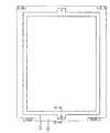
【図1】 図1は従来の液晶モジュールを上から見た平面図である。
【図2】 図2は図1で線″AーA′″に沿って切り取って表す断面図である。
【図3】 図3は図1に図示されたバックライトアレイの構成を詳細に表す断面図である。
【図4】 図4は本発明の実施例による液晶モジュールを上から見た平面図である。
【図5】 図5は図4で線″BーB′″に沿って切り取って表す断面図である。
【図6】 図6は本発明の異なる実施例による液晶モジュールの分解斜視図である。
【図7】 図7は図6に図示された液晶モジュールで光学シートの固定部を詳細に表すための平面図である。
【図8】 図8は図7で線″CーC′″に沿って切り取って表す断面図である。
【符号の説明】
2:液晶パネル
4、24、64:光学シート
4a:拡散シート
4b、4c:プリズムシート
4d、4e:保護シート
6、26:導光板
8、28:反射シート
10、30:ケーストップ
12、32、52:ガイドパネル
14、34、54:メインフレーム
21:ランプ
22:ランプ反射板
24a、32a、64a、66a:ホール
36a:突起
36:シャフト
54a:段差孔
54b:ピン
66:シリコンバッド[0001]
BACKGROUND OF THE INVENTION
The present invention relates to a liquid crystal display device, and more particularly to a liquid crystal display device that prevents damage and wrinkles of an optical sheet due to external vibration and impact.
[0002]
Normally, a liquid crystal module used in a display device of a notebook personal computer (hereinafter referred to as “NTPC”) has a large number of optical sheets (4) and a light guide plate (6) as shown in FIGS. ) And a reflective array (8) including a backlight array and a liquid crystal panel (2) laminated inside, a main frame (14), and a guide that covers the edges of the backlight array and the main frame (14) A panel (12), a liquid crystal panel (2), and a case top that covers the edge side of the guide panel (12) are provided. The main frame (14) is usually made of a molded product, but recently, it may be made of a metal having excellent heat dissipation characteristics at a high temperature, such as aluminum (AL), corresponding to a high-brightness television or monitor. . A reflection sheet (8) is positioned on the floor of the main frame (14), and a light guide plate (10) and an optical sheet (4) are laminated thereon. A liquid crystal panel (2) is mounted in the main frame (14) so as to be positioned on the optical sheet (4). As shown in FIG. 3, the backlight array includes a reflection sheet (8), a light guide plate (10), and an optical sheet (4), and a lamp reflection plate (22) for increasing the light efficiency incident on the light guide plate (10). )including.
[0003]
The optical sheet (4) includes a diffusion sheet (4a), a prism sheet (4b, 4c), and a protective sheet (4d, 4e). In the liquid crystal panel, liquid crystal is injected between two glass substrates each having a polarizing plate attached thereto, and each of the liquid crystal pixel cells arranged in a matrix form is driven by a thin film transistor ("TFT"). . The guide panel (12) is bent so as to cover the side surface of the main frame (14) and the edge side of the optical sheet (4). Similarly, the case top (10) is bent so as to cover the side surface of the guide panel (12) and the edge side of the liquid crystal panel (2). The main frame (14), the guide panel (12), and the case top (10) are fixed by screws (not shown).
[0004]
In such a liquid crystal module, the optical sheet (4) is fixed inside the main frame (14) using a double-sided adhesive tape (not shown). However, when the liquid crystal module flows or an impact is applied from the outside, the optical sheet (4) is fixed to the main frame (14) only by the double-sided adhesive tape, so that the optical sheet (14) is wrinkled or scratched (scratch ) May occur.
[0005]
[Prior art]
According to the conventional liquid crystal module structure, the assembly direction of the backlight array is reversed. That is, at the time of assembling the backlight array, the optical sheet (4), the light guide plate (6), and the reflective sheet (8) are laminated thereon with the guide panel (12) turned over, and then the reflective sheet (8 ) Is mounted and fixed on the main frame (14). As described above, since the backlight array is assembled in the reverse direction, the conventional liquid crystal module has a problem that the defect rate is high and the productivity is low.
[0006]
[Problems to be solved by the invention]
In view of the above problems, an object of the present invention is to provide a liquid crystal display device that prevents damage and wrinkles of an optical sheet even when subjected to external vibration and impact.
[0007]
[Means for Solving the Problems]
In order to achieve the above object, a liquid crystal display device according to the present invention includes an optical sheet included in a backlight array, a main frame on which the backlight array is mounted, and an optical sheet that is installed on the main frame to fix the optical sheet. And at least one shaft member.
[0008]
Other objects and advantages of the present invention will become apparent through the description of the preferred embodiments of the present invention with reference to the accompanying drawings.
[0009]
A preferred embodiment of the present invention will be described with reference to FIGS. 4 and 5, the liquid crystal display device according to the present invention includes a backlight array including a plurality of optical sheets (24), a light guide plate (26) and a reflective sheet (28), and a liquid crystal panel (2). A main frame (34) stacked on the main frame (34) and a shaft (36) installed on the main frame (34) for fixing the optical sheet (24). The main frame (24) is made of plastic or metal. A reflective sheet (28) is laid on the floor of the main frame (34), and shafts (36) are fixed to both sides.
[0010]
The shaft (36) is cylindrical and serves to fix and guide the optical sheet (24) on both sides of the optical sheet (24). A metal can be selected as the material of the shaft (36). The upper part of the shaft (36) is formed with a cylindrical protrusion (36a) having a smaller diameter than the lower part. And the center part of the edge side of both sides of an optical sheet (24) is extended outside, and the hole (24a) which the protrusion of a shaft (36) penetrates is formed in the center of the extension part.
[0011]
In addition, the liquid crystal display device according to the present invention includes a backlight array, a guide panel (32) that covers the edge of the main frame (34), and a case top (10) that covers the liquid crystal panel (2) and the guide panel (32). To do. The guide panel (32) has a hole (32a) through which the protrusion (36a) of the shaft (36) passes. The guide panel (32) is covered with a horizontal surface on the edge side of the optical sheet (24) of the backlight array, and comes into contact with the main frame (34) and the guide panel (32) on the outside at a vertical portion. The case top (30), the guide panel (32), and the main frame (34) are fixed by screws.
[0012]
The optical sheet (24) is fixed by the shaft (36) fixed on the main frame (34). 24) can be prevented from being damaged or generating wrinkles due to a high temperature driving environment. The backlight array is assembled in the positive direction in the main frame (34) by the fastening structure of the optical sheet (24) by the shaft (36). That is, in a state where the main frame (34) is placed so that the shaft (36) can be seen, the reflection sheet (28) and the light guide plate (26) are sequentially mounted in the main frame (34), and then the shaft (36 The optical sheet (24) is laminated on the light guide plate (24) so that the projections (36a) of the) penetrate the holes (24a). Then, a guide panel (32) is put on the laminated optical sheet (24).
[0013]
FIG. 6 shows a liquid crystal display device according to another embodiment of the present invention.
As shown in FIG. 6, the liquid crystal display device according to the present invention includes an optical sheet (64) fixed to a main frame (54), and a silicon pad (52) installed between the optical sheet (64) and the guide panel (52). 66). A reflection sheet is provided on the floor of the main frame (54), and a light guide plate, an optical sheet (64), and a liquid crystal panel are laminated thereon. The optical sheet (64) is fixed to the main frame (54) at the center of both sides. For this purpose, a step hole (54a) is formed in the center of both sides of the main frame (54), and a pin (54b) is formed in the step hole (54a). And the center part of the edge side of both sides of the optical sheet (64) is extended outward, and a hole (64a) through which the pin (36) of the main frame (54) passes is formed in the center of the extension part. The silicon pad (66) is made of an elastic silicon material, and a hole (66a) through which the pin (54b) of the main frame (54) passes is formed at the center.
[0014]
As shown in FIGS. 7 and 8, the silicon pad (66) has a hole (in the optical sheet (64) positioned between the optical sheet (64) fixed to the main frame (54) and the guide panel (52). 64a) is inserted into the pin (54b).
[0015]
Since the optical sheet (64) is fixed to the main frame (54) by pins (54b) and fixed by the guide panel (52) with an elastic silicon pad (66) in between, only the double-sided adhesive tape is used. It is less susceptible to damage than it is fixed by, and less wrinkles occur.
[0016]
DETAILED DESCRIPTION OF THE INVENTION
Hereinafter, embodiments of the present invention will be described in detail with reference to FIGS. 4 and 5, the liquid crystal display device according to the present invention includes a backlight array including a plurality of optical sheets (24), a light guide plate (26) and a reflective sheet (28), and a liquid crystal panel (2). A main frame (34) stacked on the main frame (34), and a shaft (36) installed on the main frame (34) for fixing the optical sheet (24). The main frame (24) is made of plastic or metal. A reflection sheet (28) is provided on the floor of the main frame (34), and shafts (36) are fixed to the edge sides on both sides. The shaft (36) is cylindrical and serves to fix and guide the optical sheet (24) on both sides of the optical sheet (24).
[0017]
A metal can be selected as the material of the shaft (36). The upper part of the shaft (36) is formed with a cylindrical protrusion (36a) having a smaller diameter than the lower part. And the center part of the edge side of both sides of the optical sheet (24) is extended outward, and a hole (24a) through which the protrusion of the shaft (36) passes is formed in the center of the extension part.
[0018]
In addition, the liquid crystal display device according to the present invention includes a backlight array, a guide panel (32) that covers the edge of the main frame (34), and a case top (10) that covers the liquid crystal panel (2) and the guide panel (32). To do. The guide panel (32) has a hole (32a) through which the protrusion (36a) of the shaft (36) passes. The guide panel (32) covers a part of the edge of the optical sheet (24) of the backlight array with a horizontal part, and the other vertical part contacts the main frame (34) and the guide panel (32) on the outside. The case top (30), the guide panel (32), and the main frame (34) are fixed by screws.
[0019]
Since the optical sheet (24) is fixed by the shaft (36) fixed on the main frame (34), the optical sheet (24) is more easily caused by liquid crystal module flow or external vibration than when the optical sheet (24) is fixed by the double-sided adhesive tape. 24) can be prevented from being damaged or caused by a high temperature driving environment. The backlight array is assembled in the positive direction in the main frame (34) by the fastening structure of the optical sheet (24) by the shaft (36). That is, in a state where the main frame (34) is placed so that the shaft (36) can be seen, the reflection sheet (28) and the light guide plate (26) are sequentially mounted in the main frame (34), and then the shaft (36 The optical sheet (24) is laminated on the light guide plate (24) so that the projections (36a) of the) penetrate the holes (24a). Then, a guide panel (32) is put on the laminated optical sheet (24).
[0020]
FIG. 6 shows a liquid crystal display device according to another embodiment of the present invention.
Referring to FIG. 6, the liquid crystal display according to the present invention includes an optical sheet (64) fixed to a main frame (54), and a silicon pad (66) installed between the optical sheet (64) and the guide panel (52). ). A reflection sheet is provided on the floor of the main frame (54), and a light guide plate, an optical sheet (64), and a liquid crystal panel are laminated thereon. The optical sheet (64) is fixed to the main frame (54) at the center of both sides.
[0021]
For this purpose, a step hole (54a) is formed in the center of both sides of the main frame (54), and a pin (54b) is formed in the step hole (54a). And the center part of the edge side of both sides of the optical sheet (64) is extended outward, and a hole (64a) through which the pin (36) of the main frame (54) passes is formed in the center of the extension part. The silicon pad (66) is made of an elastic silicon material, and a hole (66a) through which the pin (54b) of the main frame (54) passes is formed at the center. As shown in FIGS. 7 and 8, the silicon pad (66) is positioned between the optical sheet (64) fixed to the main frame (54) and the guide panel (52). Is inserted into the pin (54b) inserted into the hole (64a).
[0022]
Since the optical sheet (64) is fixed to the main frame (54) by pins (54b) and fixed by the guide panel (52) with an elastic silicon pad (66) in between, only the double-sided adhesive tape is used. It is less likely to be damaged or wrinkled than when it is fixed by.
[0023]
【The invention's effect】
As described above, in the liquid crystal display device according to the present invention, a shaft is installed on the main frame and an optical sheet is fixed to the shaft, or an elastic silicon pad is installed between the main frame and the guide panel. Since the optical sheet is sandwiched between the frame and the guide panel, scratches caused by liquid crystal module flow and external vibration are prevented compared to when the sheet is simply fixed with double-sided adhesive tape. Can prevent wrinkles.
[0024]
Those skilled in the art can understand that various changes and modifications are possible without departing from the technical idea of the present invention through the contents described above. Therefore, the technical scope of the present invention should not be limited to the contents described in the detailed description of the specification, but should be defined by the appended claims.
[Brief description of the drawings]
FIG. 1 is a plan view of a conventional liquid crystal module as viewed from above.
FIG. 2 is a cross-sectional view taken along line “A-A ′” in FIG.
FIG. 3 is a cross-sectional view showing in detail the configuration of the backlight array shown in FIG. 1;
FIG. 4 is a plan view of a liquid crystal module according to an embodiment of the present invention as viewed from above.
5 is a cross-sectional view taken along line “BB” in FIG.
FIG. 6 is an exploded perspective view of a liquid crystal module according to another embodiment of the present invention.
FIG. 7 is a plan view illustrating in detail a fixing portion of the optical sheet in the liquid crystal module illustrated in FIG. 6;
FIG. 8 is a cross-sectional view taken along line “CC” in FIG.
[Explanation of symbols]
2:
Claims (1)
Translated fromJapanese前記バックライトアレイの光学シートの縁側を、前記液晶パネルとの間に介在するように前記光学シートの平面に対して水平方向に覆う部分と前記平面に対して垂直方向に延在して前記メインフレームの内側縁部と接する部分とを有するガイドパネルと、
液晶パネルとガイドパネルを覆うケーストップと、
を具備する液晶モジュールにおいて、
バックライトアレイに含まれる光学シートの縁部の中央から伸張された伸張部に形成された貫通孔と、前記ガイドパネルに形成された貫通孔とに挿入されることにより前記光学シートを固定し、前記メインフレーム上に設置される少なくとも一つのシャフト部材とを具備することを特徴とする液晶表示装置。A main frame in which a backlight array including an optical sheet, a light guide plate, and a reflective sheet and a liquid crystal panel are laminated inside the edge;
A portion that covers the edge side of the optical sheet of the backlight array in the horizontal direction with respect to the plane of the optical sheetso as to be interposed between the liquid crystal panel and the main sheet extending in the direction perpendicular to the plane. A guide panel having a portion in contact with the inner edge of the frame;
A case top covering the liquid crystal panel and the guide panel;
In a liquid crystal module comprising:
The optical sheet is fixedby being inserted into a through-hole formed in an extended portion extended from the center of the edge of the optical sheet included in the backlight array anda through-hole formed in the guide panel, A liquid crystal display device comprising: at least one shaft memberinstalled on the main frame .
Applications Claiming Priority (2)
| Application Number | Priority Date | Filing Date | Title |
|---|---|---|---|
| KR10-2000-0048432AKR100367011B1 (en) | 2000-08-21 | 2000-08-21 | Liquid Crystal Display |
| KR2000-48432 | 2000-08-21 |
Publications (2)
| Publication Number | Publication Date |
|---|---|
| JP2002072174A JP2002072174A (en) | 2002-03-12 |
| JP3960411B2true JP3960411B2 (en) | 2007-08-15 |
Family
ID=19684292
Family Applications (1)
| Application Number | Title | Priority Date | Filing Date |
|---|---|---|---|
| JP2001133724AExpired - LifetimeJP3960411B2 (en) | 2000-08-21 | 2001-04-27 | Liquid crystal display |
Country Status (3)
| Country | Link |
|---|---|
| US (1) | US7184110B2 (en) |
| JP (1) | JP3960411B2 (en) |
| KR (1) | KR100367011B1 (en) |
Families Citing this family (45)
| Publication number | Priority date | Publication date | Assignee | Title |
|---|---|---|---|---|
| KR20040009902A (en)* | 2002-07-26 | 2004-01-31 | 삼성전자주식회사 | Back light assembly using the same and liquid crystal display device |
| KR100892585B1 (en)* | 2002-08-09 | 2009-04-08 | 삼성전자주식회사 | Lamp assembly, light supply module using same and 3-stage separate type liquid crystal display device having same |
| KR100878206B1 (en)* | 2002-08-13 | 2009-01-13 | 삼성전자주식회사 | Optical sheet, backlight assembly and liquid crystal display device using same |
| JP3717876B2 (en)* | 2002-08-28 | 2005-11-16 | シャープ株式会社 | Liquid crystal display device |
| TWI357523B (en)* | 2003-03-10 | 2012-02-01 | Samsung Electronics Co Ltd | Backlight assembly, liquid crystal display apparat |
| KR100580551B1 (en) | 2003-06-19 | 2006-05-16 | 엘지.필립스 엘시디 주식회사 | LCD Display Module |
| JP4321191B2 (en) | 2003-09-18 | 2009-08-26 | セイコーエプソン株式会社 | Liquid crystal display |
| JP4461778B2 (en)* | 2003-11-19 | 2010-05-12 | 日本電気株式会社 | Mobile terminal device |
| JP2005321727A (en)* | 2004-05-11 | 2005-11-17 | Sony Corp | Backlight device and color liquid crystal display |
| TWI272421B (en)* | 2004-05-13 | 2007-02-01 | Au Optronics Corp | Backlight unit and liquid crystal display utilizing the same |
| EP1770416B1 (en)* | 2004-07-15 | 2012-02-22 | Sony Corporation | Color filter and color liquid crystal display device |
| JP4815781B2 (en)* | 2004-10-20 | 2011-11-16 | ソニー株式会社 | Color liquid crystal display device and backlight device |
| JP2006155929A (en)* | 2004-11-25 | 2006-06-15 | Toshiba Matsushita Display Technology Co Ltd | Surface light source apparatus and liquid crystal display |
| JP4483569B2 (en)* | 2004-12-22 | 2010-06-16 | エプソンイメージングデバイス株式会社 | Liquid crystal display |
| US20060274532A1 (en)* | 2005-01-18 | 2006-12-07 | Musco Corporation | High-reflectance strips and mounting method |
| KR101213886B1 (en)* | 2005-06-22 | 2012-12-18 | 엘지디스플레이 주식회사 | Liquid crystal display device |
| JP2007024913A (en)* | 2005-07-12 | 2007-02-01 | Sharp Corp | Liquid crystal display |
| KR101232045B1 (en)* | 2005-08-24 | 2013-02-12 | 삼성디스플레이 주식회사 | Back light assembly and liquid crystal display apparatus having the same |
| JP4726605B2 (en)* | 2005-10-21 | 2011-07-20 | シャープ株式会社 | Liquid crystal display device and optical sheet mounting method |
| KR101177909B1 (en)* | 2005-11-16 | 2012-08-28 | 엘지디스플레이 주식회사 | Backlight assembly for Liquid Crystal display and Liquid Crystal Module using thereof |
| KR101199777B1 (en)* | 2005-12-08 | 2012-11-09 | 엘지디스플레이 주식회사 | Liquid crystal display device |
| KR101195227B1 (en)* | 2005-12-14 | 2012-10-29 | 삼성디스플레이 주식회사 | Liquid crystal display |
| JP2007233251A (en)* | 2006-03-03 | 2007-09-13 | Mitsubishi Electric Corp | Display device |
| KR101283973B1 (en)* | 2006-06-16 | 2013-07-09 | 엘지디스플레이 주식회사 | Backlight unit and LC display device |
| JP2008076899A (en)* | 2006-09-22 | 2008-04-03 | Sony Corp | Backlight device and display device |
| JP4285532B2 (en)* | 2006-12-01 | 2009-06-24 | ソニー株式会社 | Backlight control device, backlight control method, and liquid crystal display device |
| KR101315868B1 (en)* | 2006-12-27 | 2013-10-08 | 엘지디스플레이 주식회사 | Liquid crystal display device and back light unit thereof |
| JP4264560B2 (en)* | 2007-01-24 | 2009-05-20 | ソニー株式会社 | Backlight device, backlight control method, and liquid crystal display device |
| KR101326579B1 (en)* | 2007-05-25 | 2013-11-20 | 엘지디스플레이 주식회사 | Liquid crystal display device |
| KR20100127177A (en)* | 2009-05-25 | 2010-12-03 | 삼성전자주식회사 | Display device backlight |
| JP2011164502A (en)* | 2010-02-15 | 2011-08-25 | Nippon Seiki Co Ltd | Liquid crystal display device |
| KR20110097086A (en)* | 2010-02-24 | 2011-08-31 | 삼성전자주식회사 | Back light assembly and display device having same |
| BR112012028346A2 (en)* | 2010-05-25 | 2017-03-21 | Sharp Kabushiki Kaisaha | lighting device, display device and television receiver. |
| JP5564345B2 (en) | 2010-06-30 | 2014-07-30 | 株式会社ジャパンディスプレイ | Display device |
| WO2012073817A1 (en)* | 2010-12-03 | 2012-06-07 | シャープ株式会社 | Illumination device, display device and television receiving device |
| TW201224584A (en)* | 2010-12-08 | 2012-06-16 | Au Optronics Corp | Display device |
| CN102913821B (en)* | 2012-10-24 | 2015-11-25 | 深圳市华星光电技术有限公司 | A kind of liquid crystal indicator and backlight module thereof |
| TWI553597B (en)* | 2013-09-24 | 2016-10-11 | 友達光電股份有限公司 | Display device with force dispersal structure |
| CN104089216B (en)* | 2014-06-05 | 2017-01-18 | 京东方科技集团股份有限公司 | Backlight and display device |
| KR20160048299A (en)* | 2014-10-23 | 2016-05-04 | 삼성디스플레이 주식회사 | Display device |
| US9829746B2 (en)* | 2014-11-19 | 2017-11-28 | Canon Kabushiki Kaisha | Display apparatus having optical sheet |
| CN204176478U (en)* | 2014-11-26 | 2015-02-25 | 京东方科技集团股份有限公司 | A kind of light guide plate locating dowel, backlight module and display unit |
| CN106681053A (en)* | 2017-01-03 | 2017-05-17 | 京东方科技集团股份有限公司 | Backlight module and liquid crystal display device |
| JP6917557B2 (en)* | 2017-03-31 | 2021-08-11 | パナソニックIpマネジメント株式会社 | Display device |
| JP7373293B2 (en) | 2019-04-12 | 2023-11-02 | 株式会社ジャパンディスプレイ | light source device |
Family Cites Families (10)
| Publication number | Priority date | Publication date | Assignee | Title |
|---|---|---|---|---|
| JPH0440221U (en)* | 1990-08-03 | 1992-04-06 | ||
| JPH0481123U (en)* | 1990-11-28 | 1992-07-15 | ||
| JPH07209644A (en)* | 1994-01-11 | 1995-08-11 | Hitachi Ltd | Illumination light source for liquid crystal display |
| JPH1020310A (en)* | 1996-07-09 | 1998-01-23 | Hitachi Ltd | Liquid crystal display |
| KR100269943B1 (en)* | 1997-03-03 | 2000-10-16 | 윤종용 | All-in-one display module |
| KR100258839B1 (en)* | 1998-01-24 | 2000-06-15 | 윤종용 | Lcd module |
| JPH11305205A (en)* | 1998-04-22 | 1999-11-05 | Hitachi Ltd | Liquid crystal display |
| US6600394B1 (en)* | 1999-09-24 | 2003-07-29 | Radio Frequency Systems, Inc. | Turnable, temperature stable dielectric loaded cavity resonator and filter |
| KR100619582B1 (en)* | 1999-10-08 | 2006-09-01 | 삼성전자주식회사 | Liquid crystal display module, liquid crystal display device employing the same, and assembly method thereof |
| KR100603850B1 (en)* | 2000-02-24 | 2006-07-24 | 엘지.필립스 엘시디 주식회사 | Light guide plate and sheet fixing structure of light distribution device for liquid crystal display |
- 2000
- 2000-08-21KRKR10-2000-0048432Apatent/KR100367011B1/ennot_activeExpired - Lifetime
- 2001
- 2001-04-27JPJP2001133724Apatent/JP3960411B2/ennot_activeExpired - Lifetime
- 2001-04-30USUS09/843,830patent/US7184110B2/ennot_activeExpired - Lifetime
Also Published As
| Publication number | Publication date |
|---|---|
| JP2002072174A (en) | 2002-03-12 |
| US7184110B2 (en) | 2007-02-27 |
| US20020024623A1 (en) | 2002-02-28 |
| KR100367011B1 (en) | 2003-01-09 |
| KR20020015238A (en) | 2002-02-27 |
Similar Documents
| Publication | Publication Date | Title |
|---|---|---|
| JP3960411B2 (en) | Liquid crystal display | |
| US8807820B2 (en) | Display apparatuses | |
| US6177971B1 (en) | Slim type notebook personal computer | |
| US7671933B2 (en) | Liquid crystal display module | |
| CN101435948B (en) | Backlight module and liquid crystal display including same | |
| KR100713643B1 (en) | LCD display module for notebook computer and its assembly method | |
| KR100493437B1 (en) | Liquid crystal display module | |
| KR20040058577A (en) | Liquid crystal display device | |
| JP4690913B2 (en) | Liquid crystal display | |
| KR100905333B1 (en) | LCD Display Module | |
| KR101200885B1 (en) | Liquid Crystal Display Module | |
| KR100493616B1 (en) | Liquid crystal display | |
| KR20060062177A (en) | LCD Display | |
| KR20040076722A (en) | Liquid crystal display module | |
| KR20040058579A (en) | Liquid crystal display module and method for assembling thereof | |
| US12235532B2 (en) | Liquid crystal display device | |
| KR100870517B1 (en) | LCD Display | |
| KR20130032470A (en) | Liquid crystal display | |
| KR100421494B1 (en) | Apparatus of back light | |
| KR100453168B1 (en) | Liquid crystal module | |
| KR100939208B1 (en) | LCD Display Module | |
| KR100926102B1 (en) | LCD Display Module | |
| CN105700228B (en) | Guide panel and backlight unit including the guide panel | |
| KR101291973B1 (en) | Liquid Crystal Display device | |
| KR20040055405A (en) | Liquid crystal display moudule |
Legal Events
| Date | Code | Title | Description |
|---|---|---|---|
| A02 | Decision of refusal | Free format text:JAPANESE INTERMEDIATE CODE: A02 Effective date:20040127 | |
| A521 | Written amendment | Free format text:JAPANESE INTERMEDIATE CODE: A523 Effective date:20040526 | |
| A521 | Written amendment | Free format text:JAPANESE INTERMEDIATE CODE: A523 Effective date:20040624 | |
| A911 | Transfer to examiner for re-examination before appeal (zenchi) | Free format text:JAPANESE INTERMEDIATE CODE: A911 Effective date:20040630 | |
| A912 | Re-examination (zenchi) completed and case transferred to appeal board | Free format text:JAPANESE INTERMEDIATE CODE: A912 Effective date:20040730 | |
| A521 | Written amendment | Free format text:JAPANESE INTERMEDIATE CODE: A523 Effective date:20070223 | |
| A61 | First payment of annual fees (during grant procedure) | Free format text:JAPANESE INTERMEDIATE CODE: A61 Effective date:20070509 | |
| R150 | Certificate of patent or registration of utility model | Free format text:JAPANESE INTERMEDIATE CODE: R150 Ref document number:3960411 Country of ref document:JP Free format text:JAPANESE INTERMEDIATE CODE: R150 | |
| FPAY | Renewal fee payment (event date is renewal date of database) | Free format text:PAYMENT UNTIL: 20100525 Year of fee payment:3 | |
| S533 | Written request for registration of change of name | Free format text:JAPANESE INTERMEDIATE CODE: R313533 | |
| R350 | Written notification of registration of transfer | Free format text:JAPANESE INTERMEDIATE CODE: R350 | |
| FPAY | Renewal fee payment (event date is renewal date of database) | Free format text:PAYMENT UNTIL: 20100525 Year of fee payment:3 | |
| S533 | Written request for registration of change of name | Free format text:JAPANESE INTERMEDIATE CODE: R313533 | |
| FPAY | Renewal fee payment (event date is renewal date of database) | Free format text:PAYMENT UNTIL: 20100525 Year of fee payment:3 | |
| R371 | Transfer withdrawn | Free format text:JAPANESE INTERMEDIATE CODE: R371 | |
| FPAY | Renewal fee payment (event date is renewal date of database) | Free format text:PAYMENT UNTIL: 20110525 Year of fee payment:4 | |
| R250 | Receipt of annual fees | Free format text:JAPANESE INTERMEDIATE CODE: R250 | |
| FPAY | Renewal fee payment (event date is renewal date of database) | Free format text:PAYMENT UNTIL: 20120525 Year of fee payment:5 | |
| R250 | Receipt of annual fees | Free format text:JAPANESE INTERMEDIATE CODE: R250 | |
| FPAY | Renewal fee payment (event date is renewal date of database) | Free format text:PAYMENT UNTIL: 20120525 Year of fee payment:5 | |
| FPAY | Renewal fee payment (event date is renewal date of database) | Free format text:PAYMENT UNTIL: 20130525 Year of fee payment:6 | |
| R250 | Receipt of annual fees | Free format text:JAPANESE INTERMEDIATE CODE: R250 | |
| FPAY | Renewal fee payment (event date is renewal date of database) | Free format text:PAYMENT UNTIL: 20130525 Year of fee payment:6 | |
| R250 | Receipt of annual fees | Free format text:JAPANESE INTERMEDIATE CODE: R250 | |
| R250 | Receipt of annual fees | Free format text:JAPANESE INTERMEDIATE CODE: R250 | |
| R250 | Receipt of annual fees | Free format text:JAPANESE INTERMEDIATE CODE: R250 | |
| R250 | Receipt of annual fees | Free format text:JAPANESE INTERMEDIATE CODE: R250 | |
| R250 | Receipt of annual fees | Free format text:JAPANESE INTERMEDIATE CODE: R250 | |
| R250 | Receipt of annual fees | Free format text:JAPANESE INTERMEDIATE CODE: R250 | |
| R250 | Receipt of annual fees | Free format text:JAPANESE INTERMEDIATE CODE: R250 | |
| R250 | Receipt of annual fees | Free format text:JAPANESE INTERMEDIATE CODE: R250 | |
| EXPY | Cancellation because of completion of term |