JP3958662B2 - Processor - Google Patents
ProcessorDownload PDFInfo
- Publication number
- JP3958662B2 JP3958662B2JP2002280077AJP2002280077AJP3958662B2JP 3958662 B2JP3958662 B2JP 3958662B2JP 2002280077 AJP2002280077 AJP 2002280077AJP 2002280077 AJP2002280077 AJP 2002280077AJP 3958662 B2JP3958662 B2JP 3958662B2
- Authority
- JP
- Japan
- Prior art keywords
- instruction
- data
- register
- decoding
- processor
- Prior art date
- Legal status (The legal status is an assumption and is not a legal conclusion. Google has not performed a legal analysis and makes no representation as to the accuracy of the status listed.)
- Expired - Lifetime
Links
Images


Classifications
- G—PHYSICS
- G06—COMPUTING OR CALCULATING; COUNTING
- G06F—ELECTRIC DIGITAL DATA PROCESSING
- G06F9/00—Arrangements for program control, e.g. control units
- G06F9/06—Arrangements for program control, e.g. control units using stored programs, i.e. using an internal store of processing equipment to receive or retain programs
- G06F9/30—Arrangements for executing machine instructions, e.g. instruction decode
- G06F9/30003—Arrangements for executing specific machine instructions
- G06F9/30007—Arrangements for executing specific machine instructions to perform operations on data operands
- G06F9/30025—Format conversion instructions, e.g. Floating-Point to Integer, decimal conversion
- G—PHYSICS
- G06—COMPUTING OR CALCULATING; COUNTING
- G06F—ELECTRIC DIGITAL DATA PROCESSING
- G06F9/00—Arrangements for program control, e.g. control units
- G06F9/06—Arrangements for program control, e.g. control units using stored programs, i.e. using an internal store of processing equipment to receive or retain programs
- G06F9/30—Arrangements for executing machine instructions, e.g. instruction decode
- G06F9/30003—Arrangements for executing specific machine instructions
- G06F9/30007—Arrangements for executing specific machine instructions to perform operations on data operands
- G06F9/3001—Arithmetic instructions
- G06F9/30014—Arithmetic instructions with variable precision
- G—PHYSICS
- G06—COMPUTING OR CALCULATING; COUNTING
- G06F—ELECTRIC DIGITAL DATA PROCESSING
- G06F9/00—Arrangements for program control, e.g. control units
- G06F9/06—Arrangements for program control, e.g. control units using stored programs, i.e. using an internal store of processing equipment to receive or retain programs
- G06F9/30—Arrangements for executing machine instructions, e.g. instruction decode
- G06F9/30003—Arrangements for executing specific machine instructions
- G06F9/30007—Arrangements for executing specific machine instructions to perform operations on data operands
- G06F9/30021—Compare instructions, e.g. Greater-Than, Equal-To, MINMAX
- G—PHYSICS
- G06—COMPUTING OR CALCULATING; COUNTING
- G06F—ELECTRIC DIGITAL DATA PROCESSING
- G06F9/00—Arrangements for program control, e.g. control units
- G06F9/06—Arrangements for program control, e.g. control units using stored programs, i.e. using an internal store of processing equipment to receive or retain programs
- G06F9/30—Arrangements for executing machine instructions, e.g. instruction decode
- G06F9/30003—Arrangements for executing specific machine instructions
- G06F9/30007—Arrangements for executing specific machine instructions to perform operations on data operands
- G06F9/30036—Instructions to perform operations on packed data, e.g. vector, tile or matrix operations
- G06F9/30038—Instructions to perform operations on packed data, e.g. vector, tile or matrix operations using a mask
- G—PHYSICS
- G06—COMPUTING OR CALCULATING; COUNTING
- G06F—ELECTRIC DIGITAL DATA PROCESSING
- G06F9/00—Arrangements for program control, e.g. control units
- G06F9/06—Arrangements for program control, e.g. control units using stored programs, i.e. using an internal store of processing equipment to receive or retain programs
- G06F9/30—Arrangements for executing machine instructions, e.g. instruction decode
- G06F9/30094—Condition code generation, e.g. Carry, Zero flag
- G—PHYSICS
- G06—COMPUTING OR CALCULATING; COUNTING
- G06F—ELECTRIC DIGITAL DATA PROCESSING
- G06F9/00—Arrangements for program control, e.g. control units
- G06F9/06—Arrangements for program control, e.g. control units using stored programs, i.e. using an internal store of processing equipment to receive or retain programs
- G06F9/30—Arrangements for executing machine instructions, e.g. instruction decode
- G06F9/30145—Instruction analysis, e.g. decoding, instruction word fields
- G06F9/3016—Decoding the operand specifier, e.g. specifier format
- G06F9/30167—Decoding the operand specifier, e.g. specifier format of immediate specifier, e.g. constants
- G—PHYSICS
- G06—COMPUTING OR CALCULATING; COUNTING
- G06F—ELECTRIC DIGITAL DATA PROCESSING
- G06F9/00—Arrangements for program control, e.g. control units
- G06F9/06—Arrangements for program control, e.g. control units using stored programs, i.e. using an internal store of processing equipment to receive or retain programs
- G06F9/30—Arrangements for executing machine instructions, e.g. instruction decode
- G06F9/38—Concurrent instruction execution, e.g. pipeline or look ahead
- G06F9/3885—Concurrent instruction execution, e.g. pipeline or look ahead using a plurality of independent parallel functional units
- G06F9/3887—Concurrent instruction execution, e.g. pipeline or look ahead using a plurality of independent parallel functional units controlled by a single instruction for multiple data lanes [SIMD]
Landscapes
- Engineering & Computer Science (AREA)
- Software Systems (AREA)
- Theoretical Computer Science (AREA)
- Physics & Mathematics (AREA)
- General Physics & Mathematics (AREA)
- General Engineering & Computer Science (AREA)
- Mathematical Physics (AREA)
- Computational Mathematics (AREA)
- Mathematical Analysis (AREA)
- Mathematical Optimization (AREA)
- Pure & Applied Mathematics (AREA)
- Executing Machine-Instructions (AREA)
- Advance Control (AREA)
Description
Translated fromJapanese【0001】
【発明の属する技術分野】
本発明は、DSPやCPU等のプロセッサに関し、特に、音声や画像等の信号処理に好適なプロセッサに関する。
【0002】
【従来の技術】
マルチメディア技術の発展に伴い、音声や画像の信号処理等に代表されるメディア処理を高速に実行するプロセッサが求められている。その要求に応える従来のプロセッサとして、SIMD(Single Instruction Multiple Data)型の命令をサポートしているプロセッサがある。例えば、米国インテル社のPentium(R)/同III/同4のMMX/SSE/SSE2等である。インテル社のMMXであれば、64ビット長のMMXレジスタに格納された最大8個の整数を対象として、1つの命令で同一のオペレーションを実行することができる。
【0003】
【発明が解決しようとする課題】
しかしながら、上記の従来のプロセッサは、メディア処理に対する多様な要求に十分に応えているとは言えないという問題がある。
【0004】
例えば、従来のプロセッサは、1つの命令で複数のデータに対する演算を実行したり、1つの命令で複数のデータをコンペアしたりすることができるものの、それら複数のコンペア結果を1つの命令で評価するということができない。例として、従来のプロセッサは、1つの命令で、32ビット長の2つのレジスタに格納されたデータどうしをバイト単位でコンペアし、その結果を4つのフラグにセットするという処理を実行するものの、1つの命令で、それら4つのフラグの値すべてがゼロであるか否かを判別することができない。そのために、4つのフラグを読み出し、すべてがゼロであるか否かを判別する複数の命令が必要となる。これでは、例えば、4つの画素値を単位として他の画素値との比較を行うたびに、その比較結果を評価するための複数の命令が必要とされ、命令数の増加を招き、画像処理の速度が低下する。
【0005】
そこで、本発明は、このような状況に鑑みてなされたものであり、高機能なSIMD演算を実行するプロセッサ、及び、デジタル信号処理を高速に実行するマルチメディア用途に適したプロセッサを提供することを目的とする。
【0007】
【課題を解決するための手段】
上記目的を達成するために、本発明に係るプロセッサは、外部メモリと接続されるプロセッサであって、データを記憶するレジスタと、命令を解読する解読手段と、解読手段による解読結果に基づいて、命令を実行する実行手段とを備え、前記実行手段は、レジスタの値を外部メモリに格納する旨の命令が前記解読手段によって解読された場合に、前記レジスタに格納されている4以上のバイトからなるワードデータのうち、上位ハーフワードの最下位1バイトと下位ハーフワードの最下位1バイトとを前記外部メモリに格納することを特徴とする。
【0008】
また、本発明に係るプロセッサは、命令を解読し実行するプロセッサであって、データを記憶するレジスタと、命令を解読する解読手段と、解読手段による解読結果に基づいて、命令を実行する実行手段とを備え、前記実行手段は、前記レジスタの上位桁にデータを格納する旨の命令が前記解読手段によって解読された場合に、前記レジスタのうち、前記上位桁を除く記憶領域の値を変更することなく、前記上位桁だけに前記データを格納することを特徴とする。
【0009】
また、本発明に係るプロセッサは、SIMD型の命令を実行するプロセッサであって、フラグを格納するフラグ記憶手段と、命令を解読する解読手段と、解読手段による解読結果に基づいて、命令を実行する実行手段とを備え、前記実行手段は、第1レジスタと第2レジスタとをオペランドとするSIMD型の演算命令が前記解読手段によって解読された場合に、前記フラグ記憶手段に格納されたフラグが第1状態を示すときには、前記第1レジスタだけをオペランドとして前記SIMD型の演算を実行し、前記フラグが第2状態を示すときには、前記第1レジスタと第2レジスタをオペランドとして前記SIMD型の演算を実行することを特徴とする。
【0010】
また、本発明に係るプロセッサは、SIMD型の命令を実行するプロセッサであって、命令を解読する解読手段と、解読手段による解読結果に基づいて、命令を実行する実行手段とを備え、前記実行手段は、複数のデータそれぞれの符号に基づいて値を生成する旨のSIMD型の命令が前記解読手段によって解読された場合に、前記複数のデータそれぞれが正、ゼロ及び負のいずれの値であるかを示すデータを生成することを特徴とする。
【0011】
また、本発明に係るプロセッサは、SIMD型の命令を実行するプロセッサであって、第1パラメータ及び第2パラメータを指定するパラメータ指定手段と、命令を解読する解読手段と、解読手段による解読結果に基づいて、命令を実行する実行手段とを備え、前記実行手段は、第1データを操作する旨の命令が前記解読手段によって解読された場合に、前記第1データを前記第1パラメータに基づいてビットシフトし、得られたシフトデータのうち、前記第2パラメータによって特定される単位長位置の複数の単位長データを出力することを特徴とする。
【0012】
また、本発明に係るプロセッサは、命令を解読し実行するプロセッサであって、命令を解読する解読手段と、解読手段による解読結果に基づいて、命令を実行する実行手段とを備え、前記実行手段は、第1及び第2データをオペランドとする加算命令が前記解読手段によって解読された場合に、前記第1データがゼロ又は正であるときには、前記第1データと前記第2データと1とを加算した結果を生成し、前記第1データが負であるときには、前記第1データと前記第2データとを加算した結果を生成することを特徴とする。
【0013】
また、本発明に係るプロセッサは、命令を解読し実行するプロセッサであって、複数のレジスタと、命令を解読する解読手段と、解読手段による解読結果に基づいて、命令を実行する実行手段とを備え、前記実行手段は、第1及び第2レジスタの値を転送する旨の命令が前記解読手段によって解読された場合に、前記第1レジスタの値を第3レジスタに格納するとともに、前記第2レジスタの値を前記第3レジスタと連続する位置に設けられた第4レジスタに格納することを特徴とする。
【0014】
また、本発明に係るプロセッサは、命令を解読し実行するプロセッサであって、条件実行命令のプレディケートに用いられる複数のフラグを記憶するフラグ記憶手段と、命令を解読する解読手段と、解読手段による解読結果に基づいて、命令を実行する実行手段とを備え、前記実行手段は、前記フラグをオペランドとするループの分岐命令が前記解読手段によって解読された場合に、ループの先頭への分岐とともに前記フラグの設定を行うことを特徴とする。また、命令を解読し実行するプロセッサであって、分岐先アドレスを格納する分岐レジスタと条件実行命令のプレディケートに用いられる複数のフラグを記憶するフラグ記憶手段と、命令を解読する解読手段と、解読手段による解読結果に基づいて、命令を実行する実行手段とを備え、前記実行手段は、前記フラグをオペランドとする分岐レジスタへの格納命令が前記解読手段によって解読された場合に、ループの先頭アドレスを前記分岐レジスタに格納するとともに前記フラグの設定を行うことを特徴とする。
【0015】
また、本発明に係るプロセッサは、SIMD型の命令を実行するプロセッサであって、命令を解読する解読手段と、解読手段による解読結果に基づいて、命令を実行する実行手段とを備え、前記実行手段は、複数のデータ対を対象として差分絶対値和を行う旨のSIMD型の命令が前記解読手段によって解読された場合に、前記複数のデータ対それぞれの差分絶対値を加算した値を生成することを特徴とする。
【0016】
また、本発明に係るプロセッサは、命令を解読し実行するプロセッサであって、命令を解読する解読手段と、解読手段による解読結果に基づいて、命令を実行する実行手段とを備え、前記実行手段は、第1及び第2データをオペランドとする飽和命令が前記解読手段によって解読された場合に、前記第1データが前記第2データによって特定される飽和値よりも大きいときには、前記飽和値を生成し、前記第1データが前記飽和値以下であるときには、前記第1データを生成することを特徴とする。
【0018】
また、本発明に係るプロセッサは、SIMD型の命令を実行するプロセッサであって、命令を解読する解読手段と、解読手段による解読結果に基づいて、命令を実行する実行手段とを備え、前記実行手段は、SIMD型の命令が前記解読手段によって解読された場合に、SIMD型の演算を行うことによって複数の演算結果を生成し、前記複数の演算結果の少なくとも1つについてビット拡張を行うことを特徴とする。
【0019】
また、本発明に係るプロセッサは、SIMD型の命令を実行するプロセッサであって、フラグを記憶するフラグ記憶手段と、命令を解読する解読手段と、解読手段による解読結果に基づいて、命令を実行する実行手段とを備え、前記実行手段は、複数のデータ対に対してSIMD型の演算を行う旨の命令が前記解読手段によって解読された場合に、前記複数のデータ対それぞれに対して、前記フラグ記憶手段に記憶されたフラグによって特定されるSIMD型の演算を行うことを特徴とする。
【0020】
なお、本発明は、このような特徴的な命令を実行するプロセッサとして実現することができるだけでなく、複数のデータ等に対する演算処理方法として実現したり、特徴的な命令を含むプログラムとして実現したりすることもできる。そして、そのようなプログラムは、CD−ROM等の記録媒体やインターネット等の伝送媒体を介して流通させることができるのは言うまでもない。
【0021】
【発明の実施の形態】
本発明に係るプロセッサのアーキテクチャについて説明する。本プロセッサの命令は通常のマイコンに比べて並列性が高く、AVメディア系信号処理技術分野をターゲットとして開発された汎用プロセッサである。携帯電話、モバイルAV機器、デジタルTV、DVD等に共通コアを使用することにより、ソフト再利用性を向上させることができる。また、本プロセッサは、高性能・高コストパフォーマンスで多くのメディア処理を実現することができ、さらに、開発効率向上を目的とした高級言語開発環境を提供する。
【0022】
図1は、本プロセッサの概略ブロック図である。本プロセッサ1は、命令制御部10、デコード部20、レジスタファイル30、演算部40、I/F部50、命令メモリ部60、データメモリ部70、拡張レジスタ部80及びI/Oインターフェース部90から構成される。演算部40は、SIMD型命令の演算を実行する算術論理・比較演算器41〜43、乗算・積和演算器44、バレルシフタ45、除算器46及び変換器47からなる。乗算・積和演算器44は、ビット精度を落とさないように、最長で65ビットで累算する。また、乗算・積和演算器44は、算術論理・比較演算器41〜43と同様、SIMD型命令の実行が可能である。更に、このプロセッサ1は、算術論理・比較演算命令が最大3並列実行可能である。
【0023】
図2は、算術論理・比較演算器41〜43の概略図を示す。算術論理・比較演算器41〜43それぞれは、ALU部41a、飽和処理部41b及びフラグ部41cから構成される。ALU部41aは、算術演算器、論理演算器、比較器、TST器からなる。対応する演算データのビット幅は、8ビット(演算器を4並列で使用)、16ビット(演算器を2並列で使用)、32ビットである(全演算器で32ビットデータ処理)。更に算術演算結果に対しては、フラグ部41c等により、オーバーフローの検出とコンディションフラグの生成が行われる。各演算器、比較器、TST器の結果は、算術右シフト、飽和処理部41bによる飽和、最大・最小値検出、絶対値生成処理が行われる。
【0024】
図3は、バレルシフタ45の構成を示すブロック図である。バレルシフタ45は、セレクタ45a、45b、上位バレルシフタ45c、下位バレルシフタ45d及び飽和処理部45eから構成され、データの算術シフト(2の補数体系のシフト)または、論理シフト(符号なしシフト)を実行する。通常は、32ビットもしくは、64ビットのデータを入出力としている。レジスタ30a、30bに格納された被シフトデータに対して、別のレジスタまたは即値でシフト量が指定される。データは、左63ビット〜右63ビットの算術または論理シフトが行われ、入力ビット長で出力される。
【0025】
また、バレルシフタ45は、SIMD型命令に対して、8、16、32、64ビットのデータをシフトすることができる。例えば、8ビットデータのシフトを4並列で処理することができる。
【0026】
算術シフトは、2の補数体系のシフトであり、加算や減算時の小数点の位置合わせや、2のべき乗の乗算(2、2の2乗、2の(−1)乗、2の(−2)乗倍など)等のために行われる。
【0027】
図4は、変換器47の構成を示すブロック図である。変換器47は、飽和ブロック(SAT)47a、BSEQブロック47b、MSKGENブロック47c、VSUMBブロック47、BCNTブロック47e及びILブロック47fから構成される。
【0028】
飽和ブロック(SAT)47aは、入力データに対する飽和処理を行う。32ビットデータを飽和処理するブロックを2つ持つことにより、2並列のSIMD型命令をサポートする。
【0029】
BSEQブロック47bは、MSBから連続する0か1をカウントする。
【0030】
MSKGENブロック47cは、指定されたビット区間を1、それ以外を0として出力する。
【0031】
VSUMBブロック47dは、入力データを指定されたビット幅に区切り、その総和を出力する。
【0032】
BCNTブロック47eは、入力データで1となっているビットの数をカウントする。
【0033】
ILブロック47fは、入力データを指定されたビット幅に区切り、各データブロックを入れ換えた値を出力する。
【0034】
図5は、除算器46の構成を示すブロック図である。除算器46は、被除数を64ビット、除数を32ビットとし、商と剰余を32ビットずつ出力する。商と剰余を求めるまでに34サイクルを必要とする。符号付き、符号なし、両方のデータを扱うことが可能である。ただし、被除数と除数において符号の有無の設定は共通とする。その他、オーバーフローフラグ、0除算フラグを出力する機能を有する。
【0035】
図6は、乗算・積和演算器44の構成を示すブロック図である。乗算・積和演算器44は、2つの32ビット乗算器(MUL)44a、44b、3つの64ビット加算器(Adder)44c〜44e、セレクタ44f及び飽和処理部(Saturation)44gから構成され、以下の乗算、積和演算を行う。
・32×32ビットのsignedの乗算、積和、積差演算
・32×32ビットのunsignedの乗算
・16×16ビットの2並列のsignedの乗算、積和、積差演算
・32×16ビットの2並列のsignedの乗算、積和、積差演算
これらの演算を整数、固定小数点フォーマット(h1、h2、w1、w2)のデータに対して行う。また、これらの演算に対し、丸め、飽和を行う。
【0036】
図7は、命令制御部10の構成を示すブロック図である。命令制御部10は、命令キャッシュ10a、アドレス管理部10b、命令バッファ10c〜10e、ジャンプバッファ10f及びローテーション部(rotation)10gから構成され、通常時及び分岐時の命令供給を行う。128ビットの命令バッファを3つ(命令バッファ10c〜10e)持つことにより、最大並列実行数に対応している。命令制御部10は、分岐処理に関しては、分岐実行前に、分岐先の命令をジャンプバッファ10fに格納しておくとともに、後述するTARレジスタに予め分岐先アドレスを格納しておく(settar命令)。したがって、分岐時においては、命令制御部10は、TARレジスタに格納された分岐先アドレス、及び、ジャンプバッファ10fに格納された分岐先命令を使用して、分岐を行う。
【0037】
なお、本プロセッサ1はVLIWアーキテクチャを持つプロセッサである。ここで、VLIWアーキテクチャとは、1つの命令語中に複数の命令(ロード、ストア、演算、分岐など)を格納し、それらを全て同時に実行するアーキテクチャである。プログラマは、並列実行可能な命令を1つの発行グループとして記述することによって、その発行グループを並列処理させることができる。本明細書では、発行グループの区切りを";;"で示す。以下に表記例を示す。
(例1)
mov r1, 0x23;;
この命令記述は、命令movのみを実行することを意味する。
(例2)
mov r1, 0x38
add r0, r1, r2
sub r3, r1, r2;;
これらの命令記述は、命令mov、add、subを3並列で実行することを意味する。
【0038】
命令制御部10は、発行グループを識別し、デコード部20に送る。デコード部20では、発行グループの命令を解析し、必要な資源を制御する。
【0039】
次に、本プロセッサ1が備えるレジスタについて説明する。
本プロセッサ1のレジスタセットは、以下の表1に示される通りである。
【表1】
また、本プロセッサ1のフラグセット(後述する条件フラグレジスタ等で管理されるフラグ)は、以下の表2に示される通りである。
【表2】
図8は、汎用レジスタ(R0〜R31)30aの構造を示す図である。汎用レジスタ(R0〜R31)30aは、実行対象となっているタスクのコンテキストの一部を構成し、データまたはアドレスを格納する32ビットのレジスタ群である。なお、汎用レジスタR30およびR31は、それぞれグローバルポインタ、スタックポインタとして、ハードウェアが使用する。
【0042】
図9は、リンクレジスタ(LR)30cの構造を示す図である。なお、このリンクレジスタ(LR)30cと関連して、本プロセッサ1は、図示されていない退避レジスタ(SVR)も備える。リンクレジスタ(LR)30cは、関数コール時のリターンアドレスを格納する32ビットのレジスタである。なお、退避レジスタ(SVR)は、関数コール時の条件フラグレジスタのコンディションフラグ(CFR.CF)を退避する16ビットのレジスタである。リンクレジスタ(LR)30cは、後述する分岐レジスタ(TAR)と同様に、ループ高速化にも使用される。下位1ビットは常に0が読み出されるが、書き込み時には0を書き込む必要がある。
【0043】
例えば、call(brl,jmpl)命令を実行した場合には、本プロセッサ1は、リンクレジスタ(LR)30cに戻りアドレスを退避し、退避レジスタ(SVR)にコンディションフラグ(CFR.CF)を退避する。また、jmp命令を実行した場合には、リンクレジスタ(LR)30cから戻りアドレス(分岐先アドレス)を取り出し、プログラムカウンタ(PC)を復帰させる。さらに、ret(jmpr)命令を実行した場合には、リンクレジスタ(LR)30cから分岐先アドレス(戻りアドレス)を取り出し、プログラムカウンタ(PC)に格納(復帰)する。さらに、退避レジスタ(SVR)からコンディションフラグを取り出し、条件フラグレジスタ(CFR)32のコンディションンフラグ領域CFR.CFに格納(復帰)する。
【0044】
図10は、分岐レジスタ(TAR)30dの構造を示す図である。分岐レジスタ(TAR)30dは、分岐ターゲットアドレスを格納する32ビットのレジスタである。主に、ループの高速化に用いられる。下位1ビットは常に0が読み出されるが、書き込み時には0を書き込む必要がある。
【0045】
例えば、jmp,jloop命令を実行した場合には、本プロセッサ1は、分岐レジスタ(TAR)30dから分岐先アドレスを取り出し、プログラムカウンタ(PC)に格納する。分岐レジスタ(TAR)30dに格納されたアドレスの命令が分岐用命令バッファに格納されている場合は、分岐ペナルティが0になる。分岐レジスタ(TAR)30dにループの先頭アドレスを格納しておくことでループを高速化することができる。
【0046】
図11は、プログラム状態レジスタ(PSR)31の構造を示す図である。プログラム状態レジスタ(PSR)31は、実行対象となっているタスクのコンテキストの一部を構成し、以下に示されるプロセッサ状態情報を格納する32ビットのレジスタである。
【0047】
ビットSWE:VMP(Virtual Multi-Processor)のLP(Logical Processor)切替えイネーブルを示す。「0」はLP切替え不許可を示し、「1」はLP切替え許可を示す。
【0048】
ビットFXP:固定小数点モードを示す。「0」はモード0を示し、「1」はモード1を示す。
【0049】
ビットIH:割込み処理フラグであり、マスカブル割込み処理中であることを示す。「1」は割込み処理中であることを示し、「0」は割込み処理中でないことを示す。割込みが発生すると自動的にセットされる。rti命令で割込みから復帰したところが、他の割込み処理中かプログラム処理中であるのかを見分けるために使用される。
【0050】
ビットEH:エラーまたはNMIを処理中であることを示すフラグである。「0」はエラー/NMI割込み処理中でないことを示し、「1」はエラー/NMI割込み処理中であることを示す。EH=1のとき、非同期エラーまたはNMIが発生した場合は、マスクされる。また、VMPイネーブル時はVMPのプレート切り替えがマスクされる。
【0051】
ビットPL[1:0]:特権レベルを示す。「00」は特権レベル0、つまり、プロセッサアブストラクションレベルを示し、「01」は特権レベル1(設定できない)を示し、「10」は特権レベル2、つまり、システムプログラムレベルを示し、「11」は特権レベル3、つまり、ユーザプログラムレベルを示す。
【0052】
ビットLPIE3:LP固有割込み3イネーブルを示す。「1」は割込み許可を示し、「0」は割込み不許可を示す。
【0053】
ビットLPIE2:LP固有割込み2イネーブルを示す。「1」は割込み許可を示し、「0」は割込み不許可を示す。
【0054】
ビットLPIE1:LP固有割込み1イネーブルを示す。「1」は割込み許可を示し、「0」は割込み不許可を示す。
【0055】
ビットLPIE0:LP固有割込み0イネーブルを示す。「1」は割込み許可を示し、「0」は割込み不許可を示す。
【0056】
ビットAEE:ミスアライメント例外イネーブルを示す。「1」はミスアライメント例外許可を示し、「0」はミスアライメント例外不許可を示す。
【0057】
ビットIE:レベル割込みイネーブルを示す。「1」はレベル割込み許可を示し、「0」はレベル割込み不許可を示す。
【0058】
ビットIM[7:0]:割込みマスクを示す。レベル0〜7まで定義され、個々のレベルでマスクすることができる。レベル0が最も高いレベルとなる。IMによりマスクされていない割込み要求のうち最も高いレベルを持った割込み要求のみがプロセッサ1に受理される。割込み要求を受理すると受理したレベル以下のレベルはハードウェアで自動的にマスクされる。IM[0]はレベル0のマスクであり、IM[1]はレベル1のマスクであり、IM[2]はレベル2のマスクであり、IM[3]はレベル3のマスクであり、IM[4]はレベル4のマスクであり、IM[5]はレベル5のマスクであり、IM[6]はレベル6のマスクであり、IM[7]はレベル7のマスクである。
【0059】
reserved:予約ビットを示す。常に0が読み出される。書き込む時は0を書き込む必要がある。
【0060】
図12は、条件フラグレジスタ(CFR)32の構造を示す図である。条件フラグレジスタ(CFR)32は、実行対象となっているタスクのコンテキストの一部を構成する32ビットのレジスタであり、コンディションフラグ(条件フラグ)、オペレーションフラグ(演算フラグ)、ベクタコンディションフラグ(ベクタ条件フラグ)、演算命令用ビット位置指定フィールド、SIMDデータアライン情報フィールドから構成される。
【0061】
ビットALN[1:0]:アラインモードを示す。valnvc命令のアラインモードを設定する。
【0062】
ビットBPO[4:0]:ビットポジションを示す。ビット位置指定の必要な命令で使用する。
【0063】
ビットVC0〜VC3:ベクタ条件フラグである。LSB側のバイトあるいはハーフワードから順にVC0に対応し、MSB側がVC3に対応する。
【0064】
ビットOVS:オーバーフローフラグ(サマリー)である。飽和発生やオーバーフロー検出でセットされる。検出されなかった場合は、命令実行前の値を保持する。クリアはソフトで行う必要がある。
【0065】
ビットCAS:キャリーフラグ(サマリー)である。addc命令でキャリーまたはsubc命令でボローが発生した場合セットされる。addc命令でキャリーもしくはsubc命令でボローが発生しなかった場合は、命令実行前の値を保持する。クリアはソフトで行う必要がある。
【0066】
ビットC0〜C7:コンディションフラグである。フラグC7は常に値が1である。フラグC7へのFALSE条件の反映(0書き込み)は無視される。
【0067】
reserved:予約ビットを示す。常に0が読み出される。書き込む時は0を書き込む必要がある。
【0068】
図13は、アキュムレータ(M0,M1)30bの構造を示す図である。このアキュムレータ(M0,M1)30bは、実行対象となっているタスクのコンテキストの一部を構成し、図13(a)に示される32ビットレジスタMH0-MH1(乗除算・積和用レジスタ(上位32ビット))と、図13(b)に示される32ビットレジスタML0-ML1乗除算・積和用レジスタ(下位32ビット)とからなる。
【0069】
レジスタMH0-MHは、乗算命令では結果の上位32ビットを格納するのに使用される。積和命令ではアキュムレータの上位32ビットとして使用される。また、ビットストリームを取り扱う場合に汎用レジスタと組み合わせて使用することができる。レジスタML0-ML1は、乗算命令では結果の下位32ビットを格納するのに使用される。積和命令ではアキュムレータの下位32ビットとして使用される。
【0070】
図14は、プログラムカウンタ(PC)33の構造を示す図である。このプログラムカウンタ(PC)33は、実行対象となっているタスクのコンテキストの一部を構成し、実行中の命令のアドレスを保持する32ビットのカウンタである。下位1ビットは常に0が格納される。
【0071】
図15は、PC退避用レジスタ(IPC)34の構造を示す図である。このPC退避用レジスタ(IPC)34は、実行対象となっているタスクのコンテキストの一部を構成する32ビットのレジスタであり、下位1ビットは常に0が読み出されるが、書き込み時には0を書き込む必要がある。
【0072】
図16は、PSR退避用レジスタ(IPSR)35の構造を示す図である。このPSR退避用レジスタ(IPSR)35は、実行対象となっているタスクのコンテキストの一部を構成し、プログラム状態レジスタ(PSR)31を退避するための32ビットのレジスタであり、プログラム状態レジスタ(PSR)31の予約ビットに対応する部分は常に0が読み出されるが、書き込み時には0を書き込む必要がある。
【0073】
次に、本プロセッサ1のメモリ空間について説明する。本プロセッサ1では、4GBのリニアなメモリ空間を32分割し、128MB単位の空間に命令SRAM(Static RAM)とデータSRAMが割り当てられる。この128MBの空間を1ブロックとして、SAR(SRAM Area Register)にアクセスしたいブロックを設定する。アクセスされたアドレスがSARで設定された空間である場合は、直接命令SRAM/データSRAMに対してアクセスを行うが、SARで設定された空間でない場合は、バスコントローラ(BCU)に対してアクセス要求を出する。BCUにはオン・チップ・メモリ(OCM)、外部メモリ、外部デバイス、I/Oポート等が接続されており、それらのデバイスに対して読み書きを行うことができる。
【0074】
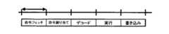
図17は、本プロセッサ1のパイプライン動作を示すタイミング図である。本プロセッサ1は、本図に示されるように、基本的に命令フェッチ、命令割り当て(ディスパッチ)、デコード、実行、書き込みの5段パイプラインで構成されている。
【0075】
図18は、本プロセッサ1による命令実行時の各パイプライン動作を示すタイミング図である。命令フェッチステージでは、プログラムカウンタ(PC)33で指定されるアドレスの命令メモリをアクセスし、命令を命令バッファ10c〜10e等に転送する。命令割り当てステージでは、分岐系命令に対する分岐先アドレス情報の出力、入力レジスタ制御信号の出力、可変長命令の割り当てを行い、命令をインストラクションレジスタ(IR)に転送する。デコードステージでは、IRをデコード部20に入力し、演算器制御信号、メモリアクセス信号を出力する。実行ステージでは、演算を実行、演算結果をデータメモリか汎用レジスタ(R0〜R31)30aに出力する。書き込みステージでは、データ転送、演算結果を汎用レジスタに格納する。
【0076】
本プロセッサ1は、VLIWアーキテクチャにより上記の処理を最高3並列で行うことができる。したがって、図18に示された動作については、本プロセッサ1は、図19に示されるタイミングで並列に実行する。
【0077】
次に、以上のように構成された本プロセッサ1の命令セットについて説明する。
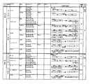
以下の表3〜表5は、本プロセッサ1が実行する命令をカテゴリー別に分類した表である。
【表3】
なお、表中の「演算器」は、その命令が使用する演算器を示す。演算器の略号の意味は次の通りである。つまり、「A」はALU命令、「B」は分岐命令、「C」は変換命令、「DIV」は除算命令、「DBGM」はデバッグ命令、「M」はメモリアクセス命令、「S1」、「S2」はシフト命令、「X1」、「X2」は乗算命令を意味する。
【0079】
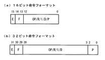
図20は、本プロセッサ1が実行する命令のフォーマットを示す図である。そのフォーマットには、図20(a)に示される16ビット命令フォーマットと、図20(b)に示される32ビット命令フォーマットとがある。
【0080】
なお、図中における略号の意味は次の通りである。つまり、「E」はエンドビット(並列実行の境界)、「F」はフォーマットビット(00、01、10:16ビット命令フォーマット、11:32ビット命令フォーマット)、「P」はプレディケート(実行条件:8個の条件フラグC0〜C7のいずれかを指定)、「OP」はオペコードフィールド、「R」はレジスタフィールド、「I」は即値フィールド、「D」ディスプースメントフィールドを意味する。なお、「E」フィールドはVLIWに特有のもので、E=0の命令は次の命令と並列に実行される。つまり、「E」フィールドによって並列度が可変のVLIWを実現している。また、プレディケートは、コンディションフラグC0〜C7の値に基づいて命令を実行させるか実行させないかを制御するフラグであり、分岐命令を用いることなく選択的な実行を可能にする高速化技術の一つである。
【0081】
図21〜図36は、本プロセッサ1が実行する命令の概略的な機能を説明する図である。つまり、図21は、カテゴリー「ALUadd(加算)系」に属する命令を説明する図であり、図22は、カテゴリー「ALUsub(減算)系」に属する命令を説明する図であり、図23は、カテゴリー「ALUlogic(論理演算)系ほか」に属する命令を説明する図であり、図24は、カテゴリー「CMP(比較演算)系」に属する命令を説明する図であり、図25は、カテゴリー「mul(乗算)系」に属する命令を説明する図であり、図26は、カテゴリー「mac(積和演算)系」に属する命令を説明する図であり、図27は、カテゴリー「msu(積差演算)系」に属する命令を説明する図であり、図28は、カテゴリー「MEMld(メモリ読み出し)系」に属する命令を説明する図であり、図29は、カテゴリー「MEMstore(メモリ書き出し)系」に属する命令を説明する図であり、図30は、カテゴリー「BRA(分岐)系」に属する命令を説明する図であり、図31は、カテゴリー「BSasl(算術バレルシフト)系ほか」に属する命令を説明する図であり、図32は、カテゴリー「BSlsr(論理バレルシフト)系ほか」に属する命令を説明する図であり、図33は、カテゴリー「CNVvaln(算術変換)系」に属する命令を説明する図であり、図34は、カテゴリー「CNV(一般変換)系」に属する命令を説明する図であり、図35は、カテゴリー「SATvlpk(飽和処理)系」に属する命令を説明する図であり、図36は、カテゴリー「ETC(その他)系」に属する命令を説明する図である。
【0082】
これらの図において、項目「SIMD」は、その命令の型(SISD(SINGLE)かSIMDかの区別)を示し、項目「サイズ」は、演算の対象となる個々のオペランドのサイズを示し、項目「命令」は、その命令のオペコードを示し、項目「オペランド」は、その命令のオペランドを示し、項目「CFR」は、条件フラグレジスタの変化を示し、項目「PSR」は、プロセッサ状態レジスタの変化を示し、項目「代表的な動作」は、動作の概要を示し、項目「演算器」は、使用される演算器を示し、項目「3116」は、命令のサイズを示す。
【0083】
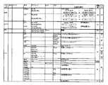
次に、いくつかの特徴的な命令について、本プロセッサ1の動作を説明する。なお、各命令の動作の説明に用いられている各種記号の意味は、以下の表6〜表10の通りである。
【表6】
[命令vcchk]
命令vcchkは、SIMD型比較命令(vcmpCCbなど)による結果が全て0かどうかを判別し、その結果を条件フラグレジスタ(CFR)32にセットするSIMD型の命令である。例えば、
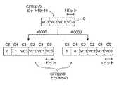
vcchk
であれば、プロセッサ1は、図37に示されるように、条件フラグレジスタ(CFR)32のベクタ条件フラグVC0〜VC3(110)が全て0であるか判定し、全て0である場合に、条件フラグレジスタ(CFR)32のコンディションフラグC4及びC5をそれぞれ1及び0にセットし、そうでない場合に、コンディションフラグC4及びC5をそれぞれ0及び1にセットする。そして、コンディションフラグC0〜C3には、ベクタ条件フラグVC0〜VC3を格納する。詳細な動作は図38に示される通りである。
【0085】
この命令によって、SIMD型比較命令の結果(特に、一致・不一致)の取り出しが早くなる。ファイル中のEOF(End Of File)の検出などに効果的である。
【0086】
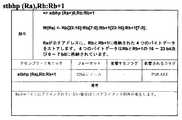
[命令stbh、stbhp]
命令stbhは、1つのレジスタに格納された2つのバイトデータ(上位16ビットに格納されたバイトデータと下位16ビットに格納されたバイトデータ)をメモリ等に格納する命令であり、命令ldbhに対応する(反対方向にデータを転送する)命令である。例えば、
stbh (Ra),Rb
であれば、プロセッサ1は、I/F部50等により、図39に示されるように、レジスタRaが示すアドレスの記憶領域に、レジスタRbに格納された2つのバイトデータ(レジスタRbの第16〜23ビット及び第0〜7ビット)をストアする。詳細な動作は図40に示される通りである。
【0087】
命令stbhpは、2つのレジスタ(ペアレジスタ)に格納された4つのバイトデータ(各レジスタの上位16ビットに格納されたバイトデータと下位16ビットに格納されたバイトデータ)をメモリ等に格納する命令であり、命令ldbhpに対応する(反対方向にデータを転送する)命令である。例えば、
stbhp (Ra),Rb:Rb+1
であれば、プロセッサ1は、I/F部50等により、図41に示されるように、レジスタRaが示すアドレスの記憶領域に、レジスタRb及びRb+1に格納された4つのバイトデータ(各レジスタの第16〜23ビット及び第0〜7ビット)をストアする。詳細な動作は図42に示される通りである。
【0088】
これらの命令によって、バイトデータを16ビットSIMD型で扱う場合に、データの型変換が不要となり、処理が高速化される。
【0089】
[命令sethi]
命令sethiは、レジスタの下位16ビットを変更することなく、上位16ビットに即値を格納する命令である。例えば、
sethi Ra,I16
であれば、プロセッサ1は、図43に示されるように、レジスタRaの上位16ビットに16ビットの即値(I16)を格納する。このとき、レジスタRaの下位16ビットは変化しない。詳細な動作は図44に示される通りである。
【0090】
この命令によって、命令「mov Rb,I16」と組み合わせることで、32ビット即値をレジスタに設定することが可能となる。
【0091】
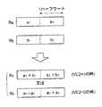
[命令vaddhvc、vaddrhvc]
命令vaddhvcは、ベクタ条件フラグの値によって、加算するソースを切り替えるSIMD型の命令である。例えば、
vaddhvc Rc,Ra,Rb
であれば、プロセッサ1は、演算部40等により、図45に示されるように、ハーフワードベクタ形式で、レジスタRaの値と、レジスタRa又はRbの値とを加算し、その結果をレジスタRcに格納する。このとき、レジスタRa及びRbの値のいずれを加算するかは、ベクタ条件フラグVC2の値による。具体的には、ベクタ条件フラグVC2=1の場合は、レジスタRaの値とレジスタRbの値とを加算し、VC2=0の場合は、レジスタRaの値とレジスタRaの値とを加算する。詳細な動作は図46に示される通りである。
【0092】
この命令は、画像処理における動き補償に有効である。加算結果レジスタRcの値を2で除した値がレジスタRa、あるいは、レジスタRaとRbの平均値となるので、図47に示されるように、動き補償のハーフペル(半画素単位の動き補償)において、整数画素及び半画素を問わずに同一プログラムで処理することができるというメリットがある。
【0093】
なお、命令vaddrhvcは、上記命令vaddhvcによる処理に、加算結果を丸める処理を付加したものに相当する。例えば、
vaddrhvc Rc,Ra,Rb
であれば、プロセッサ1は、算術論理・比較演算器41等により、図48に示されるように、ハーフワードベクタ形式で、レジスタRaの値と、レジスタRa又はRbの値とを加算し、さらに、丸めのための1を加算し、その結果をレジスタRcに格納する。他の動作は、命令vaddhvcと同様である。詳細な動作は図49に示される通りである。
この命令も、画像処理における動き補償に有効であることは言うまでもない。
【0094】
なお、上記命令vaddhvc及び命令vaddrhvcそれぞれの機能として、1ビット右シフト(2で割る処理)を付加してもよい。これによって、プロセッサは、整数画素又は半画素の画素値を直接算出することが可能となる。
【0095】
また、上記命令vaddhvc及び命令vaddrhvcの機能を併せ持つ命令を定義してもよい。例えば、コンディションフラグの値によって、命令vaddhvc及び命令vaddhrvcのいずれかの動作を行う新たな命令を設けてもよい。これによって、丸めあり・なしのいずれの場合も同一プログラムで処理することができる。
【0096】
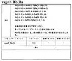
[命令vsgnh]
命令vsgnhは、レジスタの符号(正/負)及びゼロによって値を生成するSIMD型の命令である。例えば、
vsgnh Ra,Rb
であれば、プロセッサ1は、図50に示されるように、ハーフワードベクタ形式で、レジスタRaの値が正の場合は1を、負の場合は−1を、0の場合は0を、レジスタRbに格納する。詳細な動作は図51に示される通りである。
【0097】
この命令は、ある値が正のときに1、負のときに−1、ゼロのときに0を出力するので、画像処理における逆量子化に有効である。特に、本プロセッサ1では、SIMD型で演算しにくいものを高速化することが可能となる。
【0098】
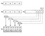
[命令valnvc1、valnvc2、valnvc3、valnvc4]
命令valnv1は、データをバイトアラインし、ベクタ条件フラグによって取り出すバイトデータを変更するSIMD型の命令である。例えば、
valnvc1 Rc,Ra,Rb
であれば、プロセッサ1は、図52に示されるように、条件フラグレジスタ(CFR)32のビットALN[1:0]の値に応じてレジスタRaとレジスタRbとを連結したビット列をシフトさせることでバイトアラインし、ベクタ条件フラグVC0の値に応じて取り出した4つのバイトデータをレジスタRcに格納する。具体的には、ベクタ条件フラグVC0=0の場合は、バイトアラインした後のデータから、4つのバイトデータa,a,b,bを取り出してレジスタRcに格納し、ベクタ条件フラグVC0=1の場合は、4つのバイトデータa,b,b,cを取り出してレジスタRcに格納する。詳細な動作は図53に示される通りである。
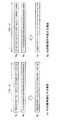
【0099】
この命令は、画像処理における動き補償に有効である。ハーフワードベクタ単位で、加算結果レジスタRcの値を2で除した値がa及びb、あるいは、(a+b)/2及び(b+c)/2に等しい値となるので、図47に示されるように、動き補償のハーフペル(半画素単位の動き補償)において、整数画素及び半画素を問わずに同一プログラムで処理することができるというメリットがある。
【0100】
なお、命令valnvc2、valnvc3及びvalnvc4は、図52に示されるように、上記命令valnvc1と基本的な動作は同じであり、バイトアラインされたデータから取り出す位置が異なるだけである。詳細な動作は、それぞれ、図54、図55、図56に示される通りである。よって、これらの命令も、画像処理における動き補償に有効であるのは言うまでもない。
【0101】
なお、本発明は、アライン等の単位がバイトに限られるものではなく、バイトに代えて、ハーフワードやハーフバイトなどでもよい。
【0102】
[命令addarvw]
命令addarvwは、2つの値を加算し、加算対象の一方が正である場合には更に1を加算する命令である。例えば、
addarvw Rc,Rb,Ra
であれば、プロセッサ1は、算術論理・比較演算器41等により、図57に示されるように、レジスタRaの値とレジスタRbの値とを加算する。このとき、レジスタRaの値が正である場合には、さらに、1を加算する。詳細な動作は図58に示される通りである。
【0103】
この命令は、「絶対値丸め(away from zero)」に有効である。図59に示されるように、絶対値丸めの対象となる値をレジスタRaに格納しておくとともに、レジスタRbに、絶対値丸めを行うビットよりも下位のビットに相当するビットを1で埋めた値を格納しておく。その上で、上記命令を実行すると、レジスタRaの値(ここでは、最上位ビットが符号ビットで、最上位から第2ビット目と第3ビット目の間に小数点が位置する固定小数点データ)に対して絶対値丸めを行った結果がレジスタRcに格納される。図58に示される例では、レジスタRcの上位2ビットのほかをマスクすることにより、+0.5に対して+1が得られ、−0.5に対して−1が得られ、絶対値丸めが実現されている。したがって、この命令は、画像処理における絶対値丸めに有効である。
【0104】
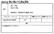
[命令movp]
命令movpは、任意の2つのレジスタの値を連続する2つのレジスタに転送する命令である。例えば、
movp Rc:Rc+1,Ra,Rb
であれば、プロセッサ1は、I/F部50等により、図60に示されるように、レジスタRaの値をレジスタRcに転送し、レジスタRbの値をレジスタRc+1に転送する。詳細な動作は図61に示される通りである。
【0105】
この命令は、独立した2つのレジスタの移動を1サイクルで行うので、例えば、ループの内部において、ループ内のサイクル数を減らすという効果を発揮し得る。また、この命令によれば、レジスタリネーミング(レジスタの値の破壊)がないので、ループの世代間(イタレーション間)でのデータの移動を行う際にも有効である。
【0106】
なお、本発明は、演算の種類が転送(mov)に限られるものではなく、一項演算(negなど)や二項演算(add)でもよい。たとえば、任意の2つのレジスタ(R0,R6)と連続する2つのレジスタ(R2,R3)を指定した加算命令であれば、2つの加算オペレーション「R0+R2→R2」及び「R6+R3→R3」が1つの命令(1つのサイクル)で実行される。
【0107】
[命令jloop、settar]
命令jloopは、ループにおける分岐とコンディションフラグ(ここでは、プレディケート)の設定とを行う命令である。例えば、
jloop C6,Cm,TAR,Ra
であれば、プロセッサ1は、アドレス管理部10b等により、(1)コンディションフラグCmに1をセットし、(2)レジスタRaの値が0より小さい場合にコンディションフラグC6に0をセットし、(3)レジスタRaの値に−1を加算し、レジスタRaに格納し、(4)分岐レジスタ(TAR)30dが示すアドレスに分岐する。ジャンプバッファ10f(分岐用命令バッファ)に分岐用命令が充填されていない場合は、分岐先の命令を充填する。詳細な動作は図62に示される通りである。
【0108】
一方、命令settarは、分岐先アドレスを分岐レジスタ(TAR)30dに格納するとともにコンディションフラグ(ここでは、プレディケート)の設定を行う命令である。例えば、
settar C6,Cm,D9
であれば、プロセッサ1は、アドレス管理部10b等により、(1)プログラムカウンタ(PC)33とディスプレースメント値(D9)を加算したアドレスを分岐レジスタ(TAR)30dに格納し、(2)そのアドレスの命令をフェッチしてジャンプバッファ10f(分岐用命令バッファ)に格納し、(3)コンディションフラグC6を1に、コンディションフラグCmを0にセットする。詳細な動作は図63に示される通りである。
【0109】
これらの命令jloop及び命令settarは、プロログエピログ除去型(以下、プロエピ除去型)のソフトウェアパイプライニングによるループの高速化に有効な命令であり、通常、対で用いられる。なお、ソフトウェアパイプライニングは、コンパイラによるループ高速化手法の1つであり、ループ構造をプロログ部、カーネル部、 エピログ部に変換し、カーネル部については、各イタレーション(繰り返し)をその前後のイタレーションとオーバーラップさせることで、複数の命令が効率的に並列実行されることを可能にする。
【0110】
また、プロエピ除去型とは、図64に示されるように、プロログ部及びエピログ部をプレディケートによる条件実行命令とすることで、プロログ部とエピログ部とを見かけ上、除去することである。図64では、プロエピ除去型2ステージソフトウェアパイプライニングにおいて、コンディションフラグC6とC4は、それぞれ、エピログ命令(ステージ2)用、プロログ命令(ステージ1)用のプレディケートとなっている。
【0111】
以下、これらの命令jloop及び命令settarが持つフラグ転送機能(コンディションフラグCmの設定)の意義について、フラグ転送機能を持たない通常の命令jloop及び命令settarと比較しながら説明する。
【0112】
本実施の形態における上記命令jloop及び命令settarがプロセッサ1の命令セットにない場合、つまり、通常の命令jloop及び命令settarだけが命令セットに含まれる場合には、コンディションフラグCmの転送は、命令jloop及び命令settarとは別個独立に行う必要がある。そのために、
(1)本来のループ実行とは無関係のフラグ転送命令が増加し、プロエピ除去型ソフトウェアパイプライニングによる性能低下を招く、
(2)フラグ間のデータ依存関係が増加し、フラグ間のデータ依存及び配置制限等により性能低下を招く、
(3)フラグ間転送命令を備える必要性が生じる、つまり、本来必要とならないフラグ間転送命令を命令セットに備える必要が出現し、命令セットのビットフィールドの圧迫を招くという問題がある。
【0113】
例えば、いま、図65に示されるC言語のソースプログラムに対して、通常の命令jloop及び命令settarを用いた場合には、コンパイラは、プロエピ除去型のソフトウェアパイプライニングによって、図66に示される機械語プログラムを生成する。この機械語プログラムのループ部分(ラベルL00023〜命令jloopまで)から分かるように、コンディションフラグC4をセットする命令(命令cmpeq)が必要となってくるために、ループ実行に3サイクル要している。さらに、コンディションフラグC4のセット及びリセットのための2命令が必要となっており、プロエピ除去の効果が減っている。
【0114】
これに対して、本実施の形態の命令jloop及び命令settarが命令セットに含まれる場合には、コンパイラは、図67に示される機械語プログラムを生成する。この機械語プログラムのループ部分(ラベルL00023〜命令jloopまで)から分かるように、コンディションフラグC4のセット及びリセットがそれぞれ命令jloop及びsettarで行われ、そのための特別な命令が不要となり、ループ実行が2サイクルで済んでいる。
【0115】
このように、命令「jloop C6,Cm,TAR,Ra」及び命令「settar C6,Cm,D9」は、2ステージのプロエピ除去型ソフトウェアパイプライニングにおける実行サイクル数を削減するという効果を有する。
【0116】
なお、本プロセッサ1は、2ステージのソフトウェアパイプライニングだけでなく、3ステージのソフトウェアパイプライニングにも適用できる命令「jloop C6,C2:C4,TAR,Ra」及び命令「settar C6,C2:C4,D9」を備える。これらの命令「jloop C6,C2:C4,TAR,Ra」及び命令「settar C6,C2:C4,D9」は、上記2ステージ用の命令「jloop C6,Cm,TAR,Ra」及び命令「settar C6,Cm,D9」におけるレジスタCmがレジスタC2、C3及びC4に拡張されたものに相当する。
【0117】
つまり、
jloop C6,C2:C4,TAR,Ra
であれば、プロセッサ1は、アドレス管理部10b等により、(1)レジスタRaが0より小さい場合にコンディションフラグC4に0をセットし、(2)コンディションフラグC3の値をコンディションフラグC2に転送し、コンディションフラグC4の値をコンディションフラグC3とC6に転送し、(3)レジスタRaに−1を加算し、レジスタRaに格納し、(4)分岐レジスタ(TAR)30dが示すアドレスに分岐する。ジャンプバッファ10fに分岐先の命令が充填されていない場合は、分岐先の命令を充填する。詳細な動作は図68に示される通りである。
【0118】
また、
settar C6,C2:C4,D9
であれば、プロセッサ1は、アドレス管理部10b等により、(1)プログラムカウンタ(PC)33とディスプレースメント値(D9)を加算したアドレスを分岐レジスタ(TAR)30dに格納し、(2)そのアドレスの命令をフェッチしてジャンプバッファ10f(分岐用命令バッファ)に格納し、(3)コンディションフラグC4とC6を1に、コンディションフラグC2とC3を0にセットする。詳細な動作は図69に示される通りである。
【0119】
これらの3ステージ用の命令「jloop C6,C2:C4,TAR,Ra」及び命令「settar C6,C2:C4,D9」におけるコンディションフラグの役割は、図70に示される通りである。図70(a)に示されるように、プロエピ除去型3ステージソフトウェアパイプライニングにおいて、コンディションフラグC2、C3、C4はそれぞれステージ3用、ステージ2用、ステージ1用のプレディケートとなっている。図70(b)は、そのときのフラグ転送による実効の推移を示す図である。
【0120】
これらの命令「jloop C6,C2:C4,TAR,Ra」及び命令「settar C6,C2:C4,D9」のフラグ転送の意義を示すプログラム例は、図71〜図73に示される通りである。図71は、ソースプログラムの例を示し、図72は、このようなフラグ転送機能を持たない命令jloop及び命令settarを用いて生成した機械語プログラムの例を示し、図73は、本実施の形態におけるフラグ転送機能を持つ命令jloop及び命令settarを用いて生成した機械語プログラムの例を示す。図72と図73を比較して分かるように、本実施の形態におけるフラグ転送機能を持つ命令jloop及び命令settarを用いることで、5つの命令が不要になるとともに、ループ実行も1サイクル少なくなっている。
【0121】
なお、4ステージ以上のソフトウェアパイプライニングについても同様であり、プレディケート用のコンディションフラグを増やせばよい。
【0122】
以上の特徴的な命令に加えて、本プロセッサ1は、上記図21〜図36に列挙されていない以下の特徴的な命令を実行することができる。
【0123】
[命令vsada]
命令vsadaは、差分絶対値和を算出するSIMD型命令である。例えば、
vsada Rc,Ra,Rb,Rx
であれば、プロセッサ1は、算術論理・比較演算器41等により、図74に示されるように、レジスタRaの値とレジスタRbの値との差分をバイト単位でSIMD演算し(4組のバイトそれぞれの差分を算出し)、4つの結果それぞれの絶対値をとって加算し、その結果にレジスタRxの値を加算し、その結果をレジスタRcに格納する。詳細な動作は図75(a)に示される通りである。
【0124】
なお、プロセッサ1は、上記命令vasadaフォーマットにおける最後のオペランド(Rx)がない形式の命令についても実行する。例えば、
vsada Rc,Ra,Rb
であれば、プロセッサ1は、算術論理・比較演算器41等により、レジスタRaの値とレジスタRbの値との差分をバイト単位でSIMD演算し(4組のバイトそれぞれの差分を算出し)、4つの結果それぞれの絶対値をとって加算し、その結果をレジスタRcに格納する。詳細な動作は図75(b)に示される通りである。
【0125】
これらの命令vsadaは、命令vasubbと命令vabssumbとの複合命令である。命令vasubbは、バイト単位で、4組のSIMDデータそれぞれを減算し、その結果得られる4つの符号を条件フラグレジスタに格納するSIMD型の命令である。一方、命令vabssumbは、条件フラグレジスタに従って、バイト単位で、4組のSIMDデータそれぞれを絶対値加算し、その結果と他の4バイトデータとを加算するSIMD型の命令である。
【0126】
したがって、この命令vsadaにより、命令vasubbと命令vabssumbとを連続して用いる場合に比べ、1サイクルで差分絶対値和が算出され、演算が高速化される。このような命令vsadaは、画像処理の動き予測における差分絶対値和の算出等に有効である。
【0127】
なお、本発明は、データの単位がバイトに限られるものではなく、ハーフワードやハーフバイトなどでもよい。
【0128】
[命令satss,satsu]
命令satssは、任意の位置(桁)で、符号付の値を符号付の値に飽和させる命令である。例えば、
satss Rc,Ra,Rb
であれば、プロセッサ1は、飽和ブロック(SAT)47a等により、図76に示されるように、レジスタRaの値がレジスタRbによって特定される飽和値(レジスタRbの1の補数)よりも大きい場合には、その飽和値をレジスタRcに格納し、レジスタRaの値が飽和値以下である場合には、レジスタRaの値をレジスタRcに格納する。詳細な動作は図77(a)に示される通りである。
【0129】
一方、命令satsuは、任意の位置(桁)で、符号なしの値を符号付の値に飽和させる命令である。例えば、
satsu Rc,Ra,Rb
であれば、プロセッサ1は、飽和ブロック(SAT)47a等により、レジスタRaの値がレジスタRbによって特定される飽和値よりも大きい場合には、その飽和値をレジスタRcに格納し、レジスタRaの値が飽和値以下である場合には、レジスタRaの値をレジスタRcに格納する。詳細な動作は図77(b)に示される通りである。
【0130】
このような命令satss及び命令satsuにより、任意の位置での飽和処理が可能となる。アセンブラプログラミングの際に特定の位置に飽和位置を合わせる必要がなくなり、プログラミングが容易となる。
【0131】
[命令bytesel]
命令byteselは、バイト単位で2つのレジスタのいずれか値を選択する命令である。例えば、
bytesel Rc,Ra,Rb,Rx
であれば、プロセッサ1は、演算部40等により、図78に示されるように、レジスタRxの値に基づいて、レジスタRa及びレジスタRbの8個のバイトデータのいずれかをレジスタRcに格納するという動作をレジスタRcの4つのバイトについて並列に行う。詳細な動作は図79(a)、レジスタRxと選択されるバイトデータとの関係は図79(b)に示される通りである。
【0132】
なお、プロセッサ1は、以下のフォーマットの命令byteselについても実行する。つまり、
bytesel Rc,Ra,Rb,I12
であれば、プロセッサ1は、演算部40等により、12ビットの即値に基づいて、バイト単位で、レジスタRa及びレジスタRbの8個のバイトデータのいずれかをレジスタRcに格納するという動作をレジスタRcの4つのバイトについて並列に行う。詳細な動作は図79(c)、即値I12と選択されるバイトデータとの関係は図79(d)に示されに示される通りである。
【0133】
この命令byteselによって、バイトデータをレジスタの任意の位置に格納することができるため、データの入替繰り返しなどが高速化される。また、SIMD演算の柔軟性を増すことができるという効果もある。
【0134】
なお、上記命令「bytesel Rc,Ra,Rb,Rx」において、レジスタRxの空きビットなどを利用して、Rc[31:24]、Rc[23:16]、Rc[15:8]、Rc[7:0]それぞれへの上記バイトデータの格納/格納しないを指定可能としてもよい。これによって、レジスタRcの値を更新するかしないかをバイト単位で選択することができる。
【0135】
なお、本発明は、データの単位がバイトに限られるものではなく、ハーフワードやハーフバイトなどでもよい。
【0136】
[SIMD演算の結果を拡張する命令]
本プロセッサ1は、以上のような命令だけでなく、SIMD演算に関連する補助的な処理を行う命令を実行することもできる。
【0137】
例えば、プロセッサ1は、ある命令が与えられると、図80に示されるように、SIMD演算の結果の一部をビット拡張(符号拡張又はゼロ拡張)する補助的な処理を行う。図80は、2つのレジスタに格納された値について、ハーフワード単位で、ストレートの位置関係又はクロスの位置関係にあるデータをSIMD演算する様子を示し、図80(a)は、得られた結果の下位ハーフワードをワードに拡張する処理を示し、図80(b)は、得られた結果の上位ハーフワードをワードに拡張する処理を示している。
【0138】
なお、ストレートの位置関係にあるデータをハーフワード単位でSIMD演算する命令とは、例えば、命令vaddhなどであり、クロスの位置関係にあるデータをハーフワード単位でSIMD演算する命令とは、例えば、命令vxaddhなどである。
【0139】
また、プロセッサ1は、ある命令が与えられると、図81に示されるように、SIMD演算の結果すべてをビット拡張する補助的な処理を行う。図81は、2つのレジスタに格納された値について、ハーフワード単位で、ストレートの位置関係又はクロスの位置関係にあるデータをSIMD演算する様子を示し、得られた2つのハーフワードそれぞれをワードに拡張する処理を示している。
【0140】
このようなSIMD演算結果を拡張する命令は、SIMD演算を行った後に符号拡張又はゼロ拡張を行ってデータサイズを揃える場合に有効であり、SIMD演算と拡張処理が1サイクルで実行される。
【0141】
さらに、プロセッサ1は、SIMD演算に関連する補助的な命令として、コンディションフラグ等によって指定された種類のSIMD演算を実行することもできる。例えば、プロセッサ1は、図82に示されるように、コンディションフラグによって第1及び第2演算それぞれが「加算」及び「減算」として指定されている場合には、2つのレジスタの値に対して、ハーフワード単位で、ストレートの位置関係又はクロスの位置関係にあるデータどうしを、それぞれ、加算及び減算する。
【0142】
一例として、コンディションフラグC0及びC1が「1,0」である場合には、プロセッサ1は、算術論理・比較演算器41等により、
(1)レジスタRaの上位ハーフワードとレジスタRbの上位ハーフワードとを加算し、その結果をレジスタRcの上位ハーフワードに格納するとともに、
(2)レジスタRaの下位ハーフワードからレジスタRbの下位ハーフワードを減算し、その結果をレジスタRcの下位ハーフワードに格納する。
【0143】
このようなSIMD演算の種類が指定可能な命令は、演算の種類が固定的でなく、他の処理結果に依存して演算の種類が決定されるような処理に有効である。
【0144】
なお、本発明は、上記演算(1)及び(2)において、レジスタRbを使用しない場合に適用することができる。たとえば、
(1)レジスタRaの上位ハーフワードとレジスタRaの下位ハーフワードとを加算し、その結果をレジスタRcの上位ハーフワードに格納するとともに、
(2)レジスタRaの上位ハーフワードからレジスタRaの下位ハーフワードを減算し、その結果をレジスタRcの下位ハーフワードに格納してもよい。
【0145】
【発明の効果】
以上の説明から明らかなように、本発明に係るプロセッサは、SIMD型比較命令による結果が全て0かどうかを判別し、その結果を条件フラグにセットするというSIMD型の特徴的な命令を実行する。これによって、SIMD型比較命令の結果(特に、一致・不一致)の取り出しが早くなり、複数の画素値を単位をする比較処理が高速化されたり、ファイル中のEOFの検出などが高速化される。
【0146】
また、本発明に係るプロセッサは、1つのレジスタに格納された2つのバイトデータ(上位16ビットに格納されたバイトデータと下位16ビットに格納されたバイトデータ)をメモリ等に格納するという特徴的な命令を実行する。これによって、例えば、バイトデータを16ビットSIMD型で扱う場合に、データの型変換が不要となり、処理が高速化される。
【0147】
また、本発明に係るプロセッサは、レジスタの下位16ビットを変更することなく、上位16ビットに即値を格納するという特徴的な命令を実行する。これによって、他の命令「mov Rb,I16」と組み合わせることで、32ビット即値をレジスタに設定することが可能となる。
【0148】
また、本発明に係るプロセッサは、ベクタ条件フラグの値によって、加算するソースを切り替えるというSIMD型の特徴的な命令を実行する。これによって、動き補償のハーフペル(半画素単位の動き補償)において、整数画素及び半画素を問わずに同一プログラムで処理することが可能となる。
【0149】
また、本発明に係るプロセッサは、レジスタの符号(正/負)及びゼロによって値を生成するというSIMD型の特徴的な命令を実行する。これによって、ある値が正のときに1、負のときに−1、ゼロのときに0を出力するので、画像処理における逆量子化が高速化される。
【0150】
また、本発明に係るプロセッサは、データを単位長アラインし、ベクタ条件フラグによって取り出す単位長データを変更するというSIMD型の特徴的な命令を実行する。これによって、動き補償のハーフペル(半画素単位の動き補償)において、整数画素及び半画素を問わずに同一プログラムで処理することが可能となる。
【0151】
また、本発明に係るプロセッサは、2つの値を加算し、加算対象の一方が正である場合には更に1を加算するという特徴的な命令を実行する。これによって、画像処理における絶対値丸めが高速化される。
【0152】
また、本発明に係るプロセッサは、任意の2つのレジスタの値を連続する2つのレジスタに転送するという特徴的な命令を実行する。これによって、独立した2つのレジスタの移動を1サイクルで行うので、例えば、ループの内部において、ループ内のサイクル数を減らすという効果を発揮し得る。また、この命令によれば、レジスタリネーミング(レジスタの値の破壊)がないので、ループの世代間(イタレーション間)でのデータの移動を行う際にも有効である。
【0153】
また、本発明に係るプロセッサは、ループにおける分岐とコンディションフラグ(ここでは、プレディケート)の設定とを行うという特徴的な命令を実行する。これによって、プロログエピログ除去型のソフトウェアパイプライニングによるループの高速化が実現される。
【0154】
また、本発明に係るプロセッサは、差分絶対値和を算出するというSIMD型特徴的な命令を実行する。これによって、画像処理の動き予測における差分絶対値和の算出等が高速化される。
【0155】
また、本発明に係るプロセッサは、命令satssは、任意の位置(桁)で、符号付の値を符号付の値に飽和させるという特徴的な命令を実行する。これによって、アセンブラプログラミングの際に特定の位置に飽和位置を合わせる必要がなくなり、プログラミングが容易となる。
【0156】
また、本発明に係るプロセッサは、単位長単位で2つのレジスタのいずれか値を選択するという特徴的な命令を実行する。これによって、単位長データをレジスタの任意の位置に格納することができるため、データの入替繰り返しなどが高速化される。また、SIMD演算の柔軟性を増すことができるという効果もある。
【0157】
また、本発明に係るプロセッサは、SIMD演算をその結果を拡張するという特徴的な命令を実行する。これによって、SIMD演算を行った後にデータサイズを揃えるという処理が1サイクルで実行される。
【0158】
また、本発明に係るプロセッサは、コンディションフラグ等によって指定された種類のSIMD演算を実行することもできる。これによって、他の処理結果に依存して演算の種類が決定されるような動的な処理が同一プログラムで実現することが可能となる。
【0159】
以上のように、本発明に係るプロセッサは、高機能なSIMD演算を実行したり、マルチメディア処理に必要な各種デジタル信号処理を高速に実行することができ、携帯電話、モバイルAV機器、デジタルTV、DVD等に共通のコアプロセッサとして使用可能であり、高性能・高コストパフォーマンスなマルチメディア機器の出現が望まれる今日における実用的価値は極めて高い。
【図面の簡単な説明】
【図1】 本発明に係るプロセッサの概略ブロック図である。
【図2】 同プロセッサの算術論理・比較演算器の概略図を示す。
【図3】 同プロセッサのバレルシタの構成を示すブロック図である。
【図4】 同プロセッサの変換器の構成を示すブロック図である。
【図5】 同プロセッサの除算器の構成を示すブロック図である。
【図6】 同プロセッサの乗算・積和演算器の構成を示すブロック図である。
【図7】 同プロセッサの命令制御部の構成を示すブロック図である。
【図8】 同プロセッサの汎用レジスタ(R0〜R31)の構造を示す図である。
【図9】 同プロセッサのリンクレジスタ(LR)の構造を示す図である。
【図10】 同プロセッサの分岐レジスタ(TAR)の構造を示す図である。
【図11】 同プロセッサのプログラム状態レジスタ(PSR)の構造を示す図である。
【図12】 同プロセッサの条件フラグレジスタ(CFR)の構造を示す図である。
【図13】 同プロセッサのアキュムレータ(M0,M1)の構造を示す図である。
【図14】 同プロセッサのプログラムカウンタ(PC)の構造を示す図である。
【図15】 同プロセッサのPC退避用レジスタ(IPC)の構造を示す図である。
【図16】 同プロセッサのPSR退避用レジスタ(IPSR)の構造を示す図である。
【図17】 同プロセッサのパイプライン動作を示すタイミング図である。
【図18】 同プロセッサによる命令実行時の各パイプライン動作を示すタイミング図である。
【図19】 同プロセッサの並列動作を示す図である。
【図20】 同プロセッサが実行する命令のフォーマットを示す図である。
【図21】 カテゴリー「ALUadd(加算)系」に属する命令を説明する図である。
【図22】 カテゴリー「ALUsub(減算)系」に属する命令を説明する図である。
【図23】 カテゴリー「ALUlogic(論理演算)系ほか」に属する命令を説明する図である。
【図24】 カテゴリー「CMP(比較演算)系」に属する命令を説明する図である。
【図25】 カテゴリー「mul(乗算)系」に属する命令を説明する図である。
【図26】 カテゴリー「mac(積和演算)系」に属する命令を説明する図である。
【図27】 カテゴリー「msu(積差演算)系」に属する命令を説明する図である。
【図28】 カテゴリー「MEMld(メモリ読み出し)系」に属する命令を説明する図である。
【図29】 カテゴリー「MEMstore(メモリ書き出し)系」に属する命令を説明する図である。
【図30】 カテゴリー「BRA(分岐)系」に属する命令を説明する図である。
【図31】 カテゴリー「BSasl(算術バレルシフト)系ほか」に属する命令を説明する図である。
【図32】 カテゴリー「BSlsr(論理バレルシフト)系ほか」に属する命令を説明する図である。
【図33】 カテゴリー「CNVvaln(算術変換)系」に属する命令を説明する図である。
【図34】 カテゴリー「CNV(一般変換)系」に属する命令を説明する図である。
【図35】 カテゴリー「SATvlpk(飽和処理)系」に属する命令を説明する図である。
【図36】 カテゴリー「ETC(その他)系」に属する命令を説明する図である。
【図37】 命令「vcchk」に対するプロセッサの動作を示す図である。
【図38】 命令「vcchk」の詳細な動作を説明する図である。
【図39】 命令「stbh (Ra),Rb」に対するプロセッサの動作を示す図である。
【図40】 命令「stbh (Ra),Rb」の詳細な動作を説明する図である。
【図41】 命令「stbhp (Ra),Rb:Rb+1」に対するプロセッサの動作を示す図である。
【図42】 命令「stbhp (Ra),Rb:Rb+1」の詳細な動作を説明する図である。
【図43】 命令「sethi Ra,I16」に対するプロセッサの動作を示す図である。
【図44】 命令「sethi Ra,I16」の詳細な動作を説明する図である。
【図45】 命令「vaddhvc Rc,Ra,Rb」に対するプロセッサの動作を示す図である。
【図46】 命令「vaddhvc Rc,Ra,Rb」の詳細な動作を説明する図である。
【図47】 画像処理における動き補償を説明する。
【図48】 命令「vaddrhvc Rc,Ra,Rb」に対するプロセッサの動作を示す図である。
【図49】 命令「vaddrhvc Rc,Ra,Rb」の詳細な動作を説明する図である。
【図50】 命令「vsgnh Ra,Rb」に対するプロセッサの動作を示す図である。
【図51】 命令「vsgnh Ra,Rb」の詳細な動作を説明する図である。
【図52】 命令「valnvc1 Rc,Ra,Rb」に対するプロセッサの動作を示す図である。
【図53】 命令「valnvc1 Rc,Ra,Rb」の詳細な動作を説明する図である。
【図54】 命令「valnvc2 Rc,Ra,Rb」の詳細な動作を説明する図である。
【図55】 命令「valnvc3 Rc,Ra,Rb」の詳細な動作を説明する図である。
【図56】 命令「valnvc4 Rc,Ra,Rb」の詳細な動作を説明する図である。
【図57】 命令「addarvw Rc,Rb,Ra」に対するプロセッサの動作を示す図である。
【図58】 命令「addarvw Rc,Rb,Ra」の詳細な動作を説明する図である。
【図59】 「絶対値丸め(away from zero)」の動作を示す図である。
【図60】 命令「movp Rc:Rc+1,Ra,Rb」に対するプロセッサの動作を示す図である。
【図61】 命令「movp Rc:Rc+1,Ra,Rb」の詳細な動作を説明する図である。
【図62】 命令「jloop C6,Cm,TAR,Ra」の詳細な動作を説明する図である。
【図63】 命令「settar C6,Cm,D9」の詳細な動作を説明する図である。
【図64】 プロエピ除去型2ステージソフトウェアパイプライニングを示す図である。
【図65】 C言語のソースプログラムのリストを示す図である。
【図66】 通常の命令jloop及び命令settarを用いて生成される機械語プログラムの例を示す。
【図67】 本実施の形態の命令jloop及び命令settarを用いて生成される機械語プログラムの例を示す。
【図68】 命令「jloop C6,C2:C4,TAR,Ra」の詳細な動作を説明する図である。
【図69】 命令「settar C6,C2:C4,D9」の詳細な動作を説明する図である。
【図70】 プロエピ除去型3ステージソフトウェアパイプライニングを示す図である。
【図71】 C言語のソースプログラムのリストを示す図である。
【図72】 通常の命令jloop及び命令settarを用いて生成される機械語プログラムの例を示す。
【図73】 本実施の形態の命令jloop及び命令settarを用いて生成される機械語プログラムの例を示す。
【図74】 命令「vsada Rc,Ra,Rb,Rx」に対するプロセッサの動作を示す図である。
【図75】 (a)は、命令「vsada Rc,Ra,Rb,Rx」、(b)は、命令「vsada Rc,Ra,Rb」の詳細な動作を説明する図である。
【図76】 命令「satss Rc,Ra,Rb」に対するプロセッサの動作を示す図である。
【図77】 (a)は、命令「satss Rc,Ra,Rb」、(b)は、命令「satsu Rc,Ra,Rb」の詳細な動作を説明する図である。
【図78】 命令「bytesel Rc,Ra,Rb,Rx」に対するプロセッサの動作を示す図である。
【図79】 (a)は、命令「bytesel Rc,Ra,Rb,Rx」の詳細な動作を示し、(b)は、レジスタRxと選択されるバイトデータとの関係を示し、(c)は、命令「bytesel Rc,Ra,Rb,I12」の詳細な動作を示し、(d)は、即値I12と選択されるバイトデータとの関係を示す図である。
【図80】 SIMD演算の結果の一部をビット拡張(符号拡張又はゼロ拡張)する様子を示す図である。
【図81】 SIMD演算の結果すべてをビット拡張する様子を示す図である。
【図82】 コンディションフラグ等によって指定された種類のSIMD演算を実行する様子を示す図である。
【符号の説明】
1 プロセッサ
10 命令制御部
10a 命令キャッシュ
10b アドレス管理部
10c〜10e 命令バッファ
10f ジャンプバッファ
10g ローテーション部
20 デコード部
30 レジスタファイル
30a 汎用レジスタ(R0〜R31)
30b アキュムレータ(MH,ML)
30c リンクレジスタ(LR)
30d 分岐レジスタ(TAR)
31 プログラム状態レジスタ(PSR)
32 条件フラグレジスタ(CFR)
33 プログラムカウンタ(PC)
34 PC退避用レジスタ(IPC)
35 PSR退避用レジスタ(IPSR)
40 演算部
41〜43 算術論理・比較演算器
41a ALU部
41b 飽和処理部
41c フラグ部
44 積和演算器
44a、44b 乗算器
44c〜44e 加算器
44f セレクタ
44g 飽和処理部
45 バレルシフタ
45a、45b セレクタ
45c 上位バレルシフタ
45d 下位バレルシフタ
45e 飽和処理部
46 除算器
47 変換器
47a SATブロック
47b BSEQブロック
47c MSKGENブロック
47d VSUMBブロック
47e BCNTブロック
47f ILブロック
50 I/F部
60 命令メモリ部
70 データメモリ部
80 拡張レジスタ部
90 I/Oインターフェース部[0001]
BACKGROUND OF THE INVENTION
The present invention relates to a processor such as a DSP or a CPU, and more particularly to a processor suitable for signal processing such as sound and image.
[0002]
[Prior art]
Along with the development of multimedia technology, there is a need for a processor that can execute media processing represented by voice and image signal processing at high speed. As a conventional processor that meets the demand, there is a processor that supports a single instruction multiple data (SIMD) type instruction. For example, Pentium (R) / III // 4 MMX / SSE / SSE2 from Intel Corporation. With Intel MMX, the same operation can be executed with a single instruction for up to eight integers stored in a 64-bit MMX register.
[0003]
[Problems to be solved by the invention]
However, the above-described conventional processor has a problem that it cannot be said that it sufficiently satisfies various requests for media processing.
[0004]
For example, although a conventional processor can perform an operation on a plurality of data with one instruction or compare a plurality of data with one instruction, the plurality of comparison results are evaluated with one instruction. I can't say that. As an example, a conventional processor executes a process of comparing data stored in two 32-bit long registers in units of bytes with one instruction and setting the result in four flags. No single instruction can determine whether all four flag values are zero. For this purpose, a plurality of instructions are required to read the four flags and determine whether all are zero. In this case, for example, each time a comparison is made with other pixel values in units of four pixel values, a plurality of instructions are required to evaluate the comparison result, resulting in an increase in the number of instructions and image processing. The speed is reduced.
[0005]
Therefore, the present invention has been made in view of such a situation, and provides a processor that performs high-performance SIMD operations and a processor suitable for multimedia applications that executes digital signal processing at high speed. With the goal.
[0007]
[Means for Solving the Problems]
To achieve the above objective , According to the present inventionRupu The processor is a processor connected to an external memory, and includes a register for storing data, a decoding means for decoding an instruction, and an execution means for executing an instruction based on a result of decoding by the decoding means. When the instruction to store the register value in the external memory is decoded by the decoding means, the least significant bit of the upper half word of the word data consisting of four or more bytes stored in the register One byte and the least significant byte of the lower halfword are stored in the external memory.
[0008]
Also, the present invention relates toRupu The processor is a processor that decodes and executes an instruction, and includes a register that stores data, a decoding unit that decodes the instruction, and an execution unit that executes an instruction based on a result of decoding by the decoding unit. When the instruction to store data in the upper digit of the register is decoded by the decoding unit, the upper digit of the register is not changed without changing the value of the storage area excluding the upper digit. The data is stored only in the storage medium.
[0009]
Also, the present invention relates toRupu The processor is a processor that executes a SIMD type instruction, and includes a flag storage unit that stores a flag, a decoding unit that decodes the instruction, and an execution unit that executes the instruction based on a result of decoding by the decoding unit. When the SIMD type arithmetic instruction having the first register and the second register as operands is decoded by the decoding unit, the execution unit is configured to display a first state when the flag stored in the flag storage unit indicates the first state. The SIMD type operation is executed using only the first register as an operand, and when the flag indicates a second state, the SIMD type operation is executed using the first register and the second register as operands. And
[0010]
Also, the present invention relates toRupu The processor is a processor for executing an SIMD type instruction, and comprises a decoding means for decoding the instruction and an execution means for executing the instruction based on a result of decoding by the decoding means, wherein the execution means includes a plurality of data Generates data indicating whether each of the plurality of data is positive, zero, or negative when a SIMD type instruction for generating a value based on each sign is decoded by the decoding means It is characterized by doing.
[0011]
Also, the present invention relates toRupu The processor is a processor that executes SIMD type instructions, and executes the instructions based on the parameter specifying means for specifying the first parameter and the second parameter, the decoding means for decoding the instructions, and the result of decoding by the decoding means. And executing means for bit-shifting the first data based on the first parameter when an instruction to manipulate the first data is decoded by the decoding means. Among the shift data, a plurality of unit length data at the unit length position specified by the second parameter is output.
[0012]
Also, the present invention relates toRupu The processor is a processor that decodes and executes an instruction, and includes a decoding unit that decodes the instruction, and an execution unit that executes an instruction based on a result of decoding by the decoding unit. When an addition instruction having two data as operands is decoded by the decoding means, if the first data is zero or positive, a result of adding the first data, the second data and 1 is generated. When the first data is negative, a result of adding the first data and the second data is generated.
[0013]
Also, the present invention relates toRupu The processor is a processor that decodes and executes an instruction, and includes a plurality of registers, a decoding unit that decodes the instruction, and an execution unit that executes an instruction based on a result of decoding by the decoding unit. When the instruction to transfer the values of the first and second registers is decoded by the decoding means, the value of the first register is stored in the third register and the value of the second register is set to the first register. It is characterized in that it is stored in a fourth register provided at a position continuous with the three registers.
[0014]
Also, the present invention relates toRupu The processor is a processor that decodes and executes an instruction, based on flag storage means for storing a plurality of flags used to predicate a condition execution instruction, a decoding means for decoding the instruction, and a result of decoding by the decoding means, Execution means for executing an instruction, and the execution means sets the flag together with a branch to the head of the loop when the branch instruction of the loop having the flag as an operand is decoded by the decoding means It is characterized by. A processor for decoding and executing an instruction, a branch register for storing a branch destination address, a flag storage means for storing a plurality of flags used for predicate of a conditional execution instruction, a decoding means for decoding an instruction, and a decoding Execution means for executing an instruction based on the result of decoding by the means, wherein the execution means, when the instruction to store in the branch register using the flag as an operand is decoded by the decoding means, Is stored in the branch register and the flag is set.
[0015]
Also, the present invention relates toRupu The processor is a processor for executing an SIMD type instruction, and comprises a decoding means for decoding the instruction and an execution means for executing the instruction based on a result of decoding by the decoding means, wherein the execution means includes a plurality of data When a SIMD type instruction for performing a sum of absolute differences for a pair is decoded by the decoding means, a value obtained by adding the absolute differences of each of the plurality of data pairs is generated.
[0016]
Also, the present invention relates toRupu The processor is a processor that decodes and executes an instruction, and includes a decoding unit that decodes the instruction, and an execution unit that executes an instruction based on a result of decoding by the decoding unit. When a saturation instruction having two data as operands is decoded by the decoding means, if the first data is larger than a saturation value specified by the second data, the saturation value is generated, and the first data is generated. When is less than or equal to the saturation value, the first data is generated.
[0018]
Also, the present invention relates toRupu The processor is a processor that executes a SIMD type instruction, and includes a decoding unit that decodes the instruction, and an execution unit that executes an instruction based on a result of decoding by the decoding unit. When an instruction is decoded by the decoding means, a plurality of operation results are generated by performing SIMD type operation, and bit extension is performed on at least one of the plurality of operation results.
[0019]
Also, the present invention relates toRupu The processor is a processor that executes SIMD type instructions, and includes a flag storage unit that stores a flag, a decoding unit that decodes the instruction, and an execution unit that executes the instruction based on the result of decoding by the decoding unit. The execution means stores each of the plurality of data pairs in the flag storage means when an instruction to perform SIMD type operation on the plurality of data pairs is decoded by the decoding means. SIMD type operation specified by the flag is performed.
[0020]
The present invention can be realized not only as a processor that executes such characteristic instructions, but also as an arithmetic processing method for a plurality of data, etc., or as a program including characteristic instructions. You can also Needless to say, such a program can be distributed via a recording medium such as a CD-ROM or a transmission medium such as the Internet.
[0021]
DETAILED DESCRIPTION OF THE INVENTION
The architecture of the processor according to the present invention will be described. The instructions of this processor have higher parallelism than ordinary microcomputers, and are general-purpose processors developed for the AV media signal processing technology field. By using a common core for mobile phones, mobile AV devices, digital TVs, DVDs, etc., software reusability can be improved. In addition, this processor can realize a lot of media processing with high performance and high cost performance, and provides a high-level language development environment for the purpose of improving development efficiency.
[0022]
FIG. 1 is a schematic block diagram of the processor. The
[0023]
FIG. 2 shows a schematic diagram of the arithmetic logic / comparison arithmetic units 41-43. Each of the arithmetic logic /
[0024]
FIG. 3 is a block diagram showing the configuration of the
[0025]
In addition, the
[0026]
Arithmetic shift is a shift of 2's complement system, and alignment of decimal point at the time of addition or subtraction, multiplication by power of 2 (2, 2 squared, 2 (-1) power, 2 (-2) Etc.) etc.
[0027]
FIG. 4 is a block diagram showing the configuration of the
[0028]
The saturation block (SAT) 47a performs saturation processing on the input data. By having two blocks that saturate 32-bit data, two parallel SIMD instructions are supported.
[0029]
The
[0030]
The
[0031]
The
[0032]
The
[0033]
The IL block 47f divides the input data into a designated bit width and outputs a value obtained by replacing each data block.
[0034]
FIG. 5 is a block diagram showing a configuration of the
[0035]
FIG. 6 is a block diagram showing a configuration of the multiplication / product-
・ 32 x 32 bit signed multiplication, product sum, product difference operation
・ 32 x 32 bit unsigned multiplication
・ 16 × 16-bit 2-parallel signed multiplication, product-sum, product-difference operations
・ 32 x 16-
These operations are performed on data in integer and fixed-point format (h1, h2, w1, w2). Also, rounding and saturation are performed for these operations.
[0036]
FIG. 7 is a block diagram illustrating a configuration of the
[0037]
The
(Example 1)
mov r1, 0x23 ;;
This instruction description means that only the instruction mov is executed.
(Example 2)
mov r1, 0x38
add r0, r1, r2
sub r3, r1, r2 ;;
These instruction descriptions mean that instructions mov, add, and sub are executed in parallel.
[0038]
The
[0039]
Next, the registers included in the
The register set of the
[Table 1]
The flag set of the processor 1 (flags managed by a condition flag register or the like described later) is as shown in Table 2 below.
[Table 2]
FIG. 8 is a diagram illustrating the structure of the general-purpose registers (R0 to R31) 30a. The general-purpose registers (R0 to R31) 30a constitute a part of the context of the task to be executed, and are a 32-bit register group that stores data or addresses. The general-purpose registers R30 and R31 are used by hardware as a global pointer and a stack pointer, respectively.
[0042]
FIG. 9 is a diagram illustrating the structure of the link register (LR) 30c. In connection with the link register (LR) 30c, the
[0043]
For example, when the call (brl, jmpl) instruction is executed, the
[0044]
FIG. 10 is a diagram showing the structure of the branch register (TAR) 30d. The branch register (TAR) 30d is a 32-bit register that stores a branch target address. Mainly used to speed up loops. The lower 1 bit is always read as 0, but 0 must be written when writing.
[0045]
For example, when a jmp, jloop instruction is executed, the
[0046]
FIG. 11 is a diagram showing the structure of the program status register (PSR) 31. The program status register (PSR) 31 is a 32-bit register that constitutes a part of the context of the task to be executed and stores the processor status information shown below.
[0047]
Bit SWE: indicates an LP (Logical Processor) switching enable of VMP (Virtual Multi-Processor). “0” indicates that LP switching is not permitted, and “1” indicates that LP switching is permitted.
[0048]
Bit FXP: indicates a fixed point mode. “0” indicates
[0049]
Bit IH: This is an interrupt processing flag and indicates that maskable interrupt processing is in progress. “1” indicates that interrupt processing is in progress, and “0” indicates that interrupt processing is not in progress. Set automatically when an interrupt occurs. It is used to determine whether the place where the rti instruction has returned from the interrupt is processing another interrupt or program.
[0050]
Bit EH: a flag indicating that an error or NMI is being processed. “0” indicates that an error / NMI interrupt is not being processed, and “1” indicates that an error / NMI interrupt is being processed. When EH = 1, if an asynchronous error or NMI occurs, it is masked. When VMP is enabled, VMP plate switching is masked.
[0051]
Bit PL [1: 0]: indicates a privilege level. “00” indicates
[0052]
Bit LPIE3: indicates LP specific interrupt 3 enable. “1” indicates interrupt permission, and “0” indicates interrupt disapproval.
[0053]
Bit LPIE2: indicates LP specific interrupt 2 enable. “1” indicates interrupt permission, and “0” indicates interrupt disapproval.
[0054]
Bit LPIE1: Indicates LP specific interrupt 1 enable. “1” indicates interrupt permission, and “0” indicates interrupt disapproval.
[0055]
Bit LPIE0: indicates LP specific interrupt 0 enable. “1” indicates interrupt permission, and “0” indicates interrupt disapproval.
[0056]
Bit AEE: indicates misalignment exception enable. “1” indicates that misalignment exception is permitted, and “0” indicates that misalignment exception is not permitted.
[0057]
Bit IE indicates level interrupt enable. “1” indicates that a level interrupt is permitted, and “0” indicates that a level interrupt is not permitted.
[0058]
Bit IM [7: 0]: indicates an interrupt mask. Levels 0-7 are defined and can be masked at individual levels.
[0059]
reserved: Indicates a reserved bit. 0 is always read. When writing, it is necessary to write 0.
[0060]
FIG. 12 is a diagram showing the structure of the condition flag register (CFR) 32. The condition flag register (CFR) 32 is a 32-bit register that constitutes a part of the context of the task to be executed, and includes a condition flag (condition flag), an operation flag (operation flag), and a vector condition flag (vector). Condition flag), a bit position designation field for operation instructions, and a SIMD data alignment information field.
[0061]
Bit ALN [1: 0]: indicates an alignment mode. Sets the alignment mode of the valnvc instruction.
[0062]
Bit BPO [4: 0]: indicates a bit position. Used in instructions that require bit position specification.
[0063]
Bits VC0 to VC3: Vector condition flags. The LSB side byte or halfword sequentially corresponds to VC0, and the MSB side corresponds to VC3.
[0064]
Bit OVS: an overflow flag (summary). Set when saturation occurs or overflow is detected. If not detected, the value before instruction execution is held. Clearing must be done by software.
[0065]
Bit CAS: carry flag (summary). Set when a carry occurs with the addc instruction or a borrow occurs with the subc instruction. If no carry occurs with the addc instruction or a borrow does not occur with the subc instruction, the value before the instruction execution is retained. Clearing must be done by software.
[0066]
Bits C0 to C7: Condition flags. The value of the flag C7 is always 1. Reflecting the FALSE condition (writing 0) to the flag C7 is ignored.
[0067]
reserved: Indicates a reserved bit. 0 is always read. When writing, it is necessary to write 0.
[0068]
FIG. 13 is a diagram showing the structure of the accumulator (M0, M1) 30b. This accumulator (M0, M1) 30b constitutes a part of the context of the task to be executed, and is a 32-bit register MH0-MH1 (multiplication / multiplication / sum of products register (high order) shown in FIG. 13 (a). 32 bits)) and the 32-bit register ML0-ML1 multiplication / division / product-sum register (lower 32 bits) shown in FIG. 13 (b).
[0069]
Registers MH0-MH are used to store the upper 32 bits of the result in multiply instructions. In the product-sum instruction, it is used as the upper 32 bits of the accumulator. Further, when handling a bit stream, it can be used in combination with a general-purpose register. Registers ML0-ML1 are used in the multiply instruction to store the lower 32 bits of the result. In the product-sum instruction, it is used as the lower 32 bits of the accumulator.
[0070]
FIG. 14 is a diagram showing the structure of the program counter (PC) 33. This program counter (PC) 33 is a 32-bit counter that constitutes a part of the context of the task to be executed and holds the address of the instruction being executed. 0 is always stored in the lower 1 bit.
[0071]
FIG. 15 is a diagram showing the structure of the PC save register (IPC) 34. The PC save register (IPC) 34 is a 32-bit register that constitutes a part of the context of the task to be executed. The lower 1 bit is always read as 0, but 0 must be written when writing. There is.
[0072]
FIG. 16 is a diagram showing the structure of the PSR save register (IPSR) 35. The PSR save register (IPSR) 35 is a 32-bit register that constitutes a part of the context of the task to be executed and saves the program status register (PSR) 31. 0 is always read out from the portion corresponding to the reserved bit of (PSR) 31, but it is necessary to write 0 when writing.
[0073]
Next, the memory space of the
[0074]
FIG. 17 is a timing chart showing the pipeline operation of the
[0075]
FIG. 18 is a timing chart showing each pipeline operation when an instruction is executed by the
[0076]
The
[0077]
Next, the instruction set of the
Tables 3 to 5 below are tables in which instructions executed by the
[Table 3]
Note that “operator” in the table indicates an arithmetic unit used by the instruction. The meaning of the abbreviation of the arithmetic unit is as follows. That is, “A” is an ALU instruction, “B” is a branch instruction, “C” is a conversion instruction, “DIV” is a division instruction, “DBGM” is a debug instruction, “M” is a memory access instruction, “S1”, “ “S2” means a shift instruction, and “X1” and “X2” mean a multiplication instruction.
[0079]
FIG. 20 is a diagram showing a format of instructions executed by the
[0080]
In addition, the meaning of the symbol in the figure is as follows. That is, “E” is an end bit (parallel execution boundary), “F” is a format bit (00, 01, 10:16 bit instruction format, 11:32 bit instruction format), and “P” is a predicate (execution condition: "OP" means an operation code field, "R" means a register field, "I" means an immediate field, and "D" a displacement field. Note that the “E” field is unique to VLIW, and an instruction with E = 0 is executed in parallel with the next instruction. That is, a VLIW having a variable parallelism is realized by the “E” field. Predicate is a flag that controls whether or not an instruction is executed based on the values of the condition flags C0 to C7, and is one of high-speed technologies that enables selective execution without using a branch instruction. It is.
[0081]
FIG. 21 to FIG. 36 are diagrams for explaining the schematic functions of the instructions executed by the
[0082]
In these figures, item “SIMD” indicates the type of instruction (distinguishing between SISD (SINGLE) and SIMD), item “size” indicates the size of each operand to be operated, and item “SIMD” "Instruction" indicates the opcode of the instruction, item "operand" indicates the operand of the instruction, item "CFR" indicates a change in the condition flag register, and item "PSR" indicates a change in the processor status register The item “representative operation” indicates an outline of the operation, the item “operation unit” indicates the operation unit to be used, and the item “3116” indicates the size of the instruction.
[0083]
Next, the operation of the
[Table 6]
[Instruction vcchk]
The instruction vcchk is a SIMD type instruction that determines whether all the results of the SIMD type comparison instruction (such as vcmpCCb) are 0 and sets the result in the condition flag register (CFR) 32. For example,
vcchk
If so, the
[0085]
By this instruction, the result of the SIMD type comparison instruction (particularly, coincidence / non-coincidence) can be quickly retrieved. This is effective for detecting EOF (End Of File) in a file.
[0086]
[Instructions stbh, stbhp]
The instruction stbh is an instruction for storing two byte data stored in one register (byte data stored in the upper 16 bits and byte data stored in the lower 16 bits) in a memory or the like, and corresponds to the instruction ldbh. Command to transfer data (in the opposite direction). For example,
stbh (Ra), Rb
If so, the
[0087]
The instruction stbhp is an instruction for storing four byte data (byte data stored in the upper 16 bits of each register and byte data stored in the lower 16 bits) stored in two registers (pair registers) in a memory or the like. And corresponds to the instruction ldbhp (transfers data in the opposite direction). For example,
stbhp (Ra), Rb: Rb + 1
If so, the
[0088]
With these instructions, when byte data is handled in the 16-bit SIMD type, data type conversion becomes unnecessary, and the processing speed is increased.
[0089]
[Instruction sethi]
The instruction sethi is an instruction for storing an immediate value in the upper 16 bits without changing the lower 16 bits of the register. For example,
sethi Ra, I16
If so, the
[0090]
By combining this instruction with the instruction “mov Rb, I16”, a 32-bit immediate value can be set in the register.
[0091]
[Instructions vaddhvc, vaddrhvc]
The instruction vaddhvc is a SIMD type instruction that switches the source to be added according to the value of the vector condition flag. For example,
vaddhvc Rc, Ra, Rb
If so, the
[0092]
This command is effective for motion compensation in image processing. Since the value obtained by dividing the value of the addition result register Rc by 2 is the average value of the register Ra or the registers Ra and Rb, as shown in FIG. 47, in the half pel of motion compensation (motion compensation in units of half pixels). There is an advantage that processing can be performed by the same program regardless of the integer pixel and the half pixel.
[0093]
The instruction vaddrhvc corresponds to a process obtained by adding a process of rounding the addition result to the process according to the instruction vaddhvc. For example,
vaddrhvc Rc, Ra, Rb
If so, the
Needless to say, this command is also effective for motion compensation in image processing.
[0094]
Note that a 1-bit right shift (a process of dividing by 2) may be added as a function of each of the instruction vaddhvc and the instruction vaddrhvc. This allows the processor to directly calculate the pixel value of an integer pixel or half pixel.
[0095]
In addition, an instruction having the functions of the instruction vaddhvc and the instruction vaddrhvc may be defined. For example, a new instruction for performing either the instruction vaddhvc or the instruction vaddhrvc may be provided depending on the value of the condition flag. Thus, the same program can be used for both cases with and without rounding.
[0096]
[Instruction vsgnh]
The instruction vsgnh is a SIMD type instruction that generates a value based on the sign (positive / negative) and zero of a register. For example,
vsgnh Ra, Rb
Then, as shown in FIG. 50, the
[0097]
Since this command outputs 1 when a certain value is positive, -1 when it is negative, and 0 when it is zero, it is effective for inverse quantization in image processing. In particular, in this
[0098]
[Instructions valnvc1, valnvc2, valnvc3, valnvc4]
The instruction valnv1 is a SIMD type instruction that byte-aligns data and changes byte data taken out by a vector condition flag. For example,
valnvc1 Rc, Ra, Rb
If so, the
[0099]
This command is effective for motion compensation in image processing. Since the value obtained by dividing the value of the addition result register Rc by 2 in halfword vector units is equal to a and b, or (a + b) / 2 and (b + c) / 2, as shown in FIG. In the half pel of motion compensation (motion compensation in units of half pixels), there is an advantage that processing can be performed with the same program regardless of integer pixels and half pixels.
[0100]
As shown in FIG. 52, the instructions valnvc2, valnvc3, and valnvc4 have the same basic operations as the instruction valnvc1, except that the positions to be extracted from the byte-aligned data are different. Detailed operations are as shown in FIGS. 54, 55, and 56, respectively. Therefore, it goes without saying that these commands are also effective for motion compensation in image processing.
[0101]
In the present invention, the unit of alignment or the like is not limited to bytes, and halfwords or halfbytes may be used instead of bytes.
[0102]
[Instruction addarrvw]
The instruction addrvw is an instruction that adds two values and further adds 1 if one of the addition targets is positive. For example,
addarrvw Rc, Rb, Ra
If so, the
[0103]
This command is useful for “away from zero”. As shown in FIG. 59, the value to be rounded by the absolute value is stored in the register Ra, and the bit corresponding to the bit lower than the bit for rounding the absolute value is filled with 1 in the register Rb. Store the value. Then, when the above instruction is executed, the value of the register Ra (here, the most significant bit is a sign bit and the decimal point is located between the second and third bits from the most significant bit) The result obtained by rounding the absolute value is stored in the register Rc. In the example shown in FIG. 58, by masking other than the upper 2 bits of the register Rc, +1 is obtained for +0.5, -1 is obtained for -0.5, and absolute value rounding is performed. It has been realized. Therefore, this instruction is effective for absolute value rounding in image processing.
[0104]
[Instruction movp]
The instruction movp is an instruction that transfers the value of any two registers to two consecutive registers. For example,
movp Rc: Rc + 1, Ra, Rb
If so, the
[0105]
Since this instruction moves two independent registers in one cycle, for example, the effect of reducing the number of cycles in the loop can be exhibited in the loop. In addition, according to this instruction, there is no register renaming (destruction of register values), so that it is also effective when moving data between loop generations (between iterations).
[0106]
In the present invention, the type of calculation is not limited to transfer (mov), and one-term calculation (eg, neg) or binary calculation (add) may be used. For example, if an addition instruction designates any two registers (R0, R6) and two consecutive registers (R2, R3), two addition operations “R0 + R2 → R2” and “R6 + R3 → R3” have one It is executed with an instruction (one cycle).
[0107]
[Instruction jloop, settar]
The instruction jloop is an instruction for branching in a loop and setting a condition flag (here, predicate). For example,
jloop C6, Cm, TAR, Ra
If so, the
[0108]
On the other hand, the instruction settar is an instruction for storing a branch destination address in the branch register (TAR) 30d and setting a condition flag (here, predicate). For example,
settar C6, Cm, D9
If so, the
[0109]
These instruction jloop and instruction settar are effective instructions for speeding up the loop by prolog epilog removal type (hereinafter, proepi removal type) software pipelining, and are usually used in pairs. Software pipelining is one of the loop acceleration methods by the compiler. The loop structure is converted into a prolog part, kernel part, and epilog part, and each iteration (repetition) is repeated before and after the iteration for the kernel part. Multiple instructions can be efficiently executed in parallel.
[0110]
In addition, the pro-epi removal type means that the prolog part and the epilog part are apparently removed by using the prolog part and the epilog part as conditional execution instructions by predicates as shown in FIG. In FIG. 64, in the pro-epi removal type two-stage software pipelining, the condition flags C6 and C4 are predicates for the epilog instruction (stage 2) and the prolog instruction (stage 1), respectively.
[0111]
Hereinafter, the significance of the flag transfer function (setting of the condition flag Cm) possessed by these instructions jloop and instruction settar will be described in comparison with normal instructions jloop and instruction settar that do not have a flag transfer function.
[0112]
When the instruction jloop and the instruction settar in the present embodiment are not in the instruction set of the
(1) Flag transfer instructions unrelated to the original loop execution increase, resulting in performance degradation due to proepi elimination type software pipelining.
(2) Data dependency between flags increases, resulting in performance degradation due to data dependency between flags and placement restrictions,
(3) There is a need to provide an inter-flag transfer instruction, that is, there is a need to provide an inter-flag transfer instruction that is not necessary in the instruction set, which causes a bit field compression in the instruction set.
[0113]
For example, when the normal instruction jloop and instruction settar are used for the C language source program shown in FIG. 65, the compiler performs the machine shown in FIG. Generate a word program. As can be seen from the loop portion of this machine language program (from label L00023 to instruction jloop), an instruction (instruction cmpeq) for setting the condition flag C4 is required, so that three cycles are required for loop execution. Further, two instructions for setting and resetting the condition flag C4 are required, and the effect of removing the pro epi is reduced.
[0114]
On the other hand, when the instruction jloop and the instruction settar of the present embodiment are included in the instruction set, the compiler generates the machine language program shown in FIG. As can be seen from the loop portion of the machine language program (from label L00023 to the instruction jloop), the condition flag C4 is set and reset by the instruction jloop and settar, respectively, and a special instruction for that is not required, and the loop execution is 2 It's done with a cycle.
[0115]
As described above, the instruction “jloop C6, Cm, TAR, Ra” and the instruction “settar C6, Cm, D9” have an effect of reducing the number of execution cycles in the two-stage pro-epi removal type software pipelining.
[0116]
The
[0117]
That means
jloop C6, C2: C4, TAR, Ra
If so, the
[0118]
Also,
settar C6, C2: C4, D9
If so, the
[0119]
The role of the condition flag in the three-stage instruction “jloop C6, C2: C4, TAR, Ra” and the instruction “settar C6, C2: C4, D9” is as shown in FIG. As shown in FIG. 70A, in the pro-epi removal type three-stage software pipelining, the condition flags C2, C3, and C4 are predicates for the
[0120]
A program example showing the significance of flag transfer of these instructions “jloop C6, C2: C4, TAR, Ra” and instruction “settar C6, C2: C4, D9” is as shown in FIGS. 71 shows an example of a source program, FIG. 72 shows an example of a machine language program generated using such an instruction jloop and an instruction settar that do not have such a flag transfer function, and FIG. 73 shows this embodiment. An example of a machine language program generated using an instruction jloop having a flag transfer function and an instruction settar in FIG. As can be seen by comparing FIG. 72 and FIG. 73, by using the instruction jloop having the flag transfer function and the instruction settar in the present embodiment, five instructions become unnecessary and the loop execution is reduced by one cycle. Yes.
[0121]
The same applies to software pipelining of four or more stages, and the predicate condition flag may be increased.
[0122]
In addition to the above characteristic instructions, the
[0123]
[Instruction vssada]
The instruction vsada is a SIMD type instruction that calculates a sum of absolute differences. For example,
vsada Rc, Ra, Rb, Rx
If so, the
[0124]
Note that the
vsada Rc, Ra, Rb
If so, the
[0125]
These instructions vsada are compound instructions of the instruction vassub and the instruction vasubsum. The instruction vassub is a SIMD type instruction that subtracts four sets of SIMD data in units of bytes and stores the four codes obtained as a result in the condition flag register. On the other hand, the instruction vabssum is a SIMD type instruction that adds the absolute value of each of four sets of SIMD data in units of bytes according to the condition flag register and adds the result to the other 4-byte data.
[0126]
Therefore, by this instruction vsada, the sum of absolute differences is calculated in one cycle compared to the case where the instruction vassub and the instruction vasubsum are used successively, and the operation is speeded up. Such an instruction vsada is effective for calculating a sum of absolute differences in motion prediction of image processing.
[0127]
In the present invention, the unit of data is not limited to bytes, but may be halfwords or halfbytes.
[0128]
[Instruction satss, satsu]
The instruction satss is an instruction for saturating a signed value to a signed value at an arbitrary position (digit). For example,
satss Rc, Ra, Rb
If so, the
[0129]
On the other hand, the instruction satsu is an instruction for saturating an unsigned value to a signed value at an arbitrary position (digit). For example,
satsu Rc, Ra, Rb
If the value of the register Ra is larger than the saturation value specified by the register Rb by the saturation block (SAT) 47a or the like, the
[0130]
By such an instruction satss and an instruction satsu, saturation processing can be performed at an arbitrary position. It is not necessary to adjust the saturation position to a specific position during assembler programming, and programming is facilitated.
[0131]
[Instruction bytesel]
The instruction bytesel is an instruction that selects one of the values of two registers in byte units. For example,
bytesel Rc, Ra, Rb, Rx
If so, the
[0132]
Note that the
byteel Rc, Ra, Rb, I12
If so, the
[0133]
By this instruction bytesel, byte data can be stored in an arbitrary position of the register, so that data replacement repetition and the like are accelerated. In addition, there is an effect that the flexibility of SIMD calculation can be increased.
[0134]
In the instruction “bytesel Rc, Ra, Rb, Rx”, Rc [31:24], Rc [23:16], Rc [15: 8], Rc [ 7: 0] It may be possible to specify whether or not to store the byte data in each. As a result, whether or not to update the value of the register Rc can be selected in units of bytes.
[0135]
In the present invention, the unit of data is not limited to bytes, but may be halfwords or halfbytes.
[0136]
[Instruction to extend the result of SIMD operation]
The
[0137]
For example, when a certain instruction is given, the
[0138]
Note that the command for performing SIMD operation on data in a straight positional relationship in halfword units is, for example, the command vaddh, and the command for performing SIMD operation on data in cross positional relationship in halfword units is, for example, Instruction vxaddh and the like.
[0139]
Further, when a certain instruction is given, the
[0140]
Such an instruction for extending the SIMD operation result is effective when the data size is made uniform by performing sign extension or zero extension after the SIMD operation, and the SIMD operation and the extension process are executed in one cycle.
[0141]
Furthermore, the
[0142]
As an example, when the condition flags C0 and C1 are “1, 0”, the
(1) Add the upper halfword of the register Ra and the upper halfword of the register Rb, store the result in the upper halfword of the register Rc,
(2) Subtract the lower halfword of the register Rb from the lower halfword of the register Ra, and store the result in the lower halfword of the register Rc.
[0143]
Such an instruction that can specify the type of SIMD calculation is not fixed, and is effective for processing in which the type of calculation is determined depending on other processing results.
[0144]
The present invention can be applied to the case where the register Rb is not used in the operations (1) and (2). For example,
(1) Add the upper halfword of the register Ra and the lower halfword of the register Ra, store the result in the upper halfword of the register Rc,
(2) The lower halfword of the register Ra may be subtracted from the upper halfword of the register Ra, and the result may be stored in the lower halfword of the register Rc.
[0145]
【The invention's effect】
As is apparent from the above description, the processor according to the present invention executes a SIMD type characteristic instruction that determines whether or not all the results of the SIMD type comparison instruction are 0 and sets the result in a condition flag. . As a result, retrieval of the results (particularly, coincidence / non-coincidence) of the SIMD type comparison instruction is quickened, the comparison process for units of a plurality of pixel values is accelerated, and the detection of EOF in the file is accelerated. .
[0146]
The processor according to the present invention stores two byte data (byte data stored in upper 16 bits and byte data stored in lower 16 bits) stored in one register in a memory or the like. Execute the correct instruction. As a result, for example, when byte data is handled in the 16-bit SIMD type, data type conversion becomes unnecessary, and the processing speed is increased.
[0147]
The processor according to the present invention executes a characteristic instruction that stores an immediate value in the upper 16 bits without changing the lower 16 bits of the register. Thus, by combining with another instruction “mov Rb, I16”, a 32-bit immediate value can be set in the register.
[0148]
Also, the processor according to the present invention executes a SIMD type characteristic instruction to switch the source to be added according to the value of the vector condition flag. As a result, in the half pel of motion compensation (motion compensation in units of half pixels), it is possible to perform processing with the same program regardless of integer pixels and half pixels.
[0149]
Further, the processor according to the present invention executes a SIMD type characteristic instruction that generates a value based on the sign (positive / negative) and zero of the register. As a result, 1 is output when a certain value is positive, -1 is output when the value is negative, and 0 is output when the value is zero, thereby speeding up the inverse quantization in the image processing.
[0150]
Further, the processor according to the present invention executes SIMD type characteristic instructions for aligning data in unit length and changing the unit length data fetched by the vector condition flag. As a result, in the half pel of motion compensation (motion compensation in units of half pixels), it is possible to perform processing with the same program regardless of integer pixels and half pixels.
[0151]
In addition, the processor according to the present invention executes a characteristic instruction that adds two values and further adds 1 when one of the addition targets is positive. This speeds up the rounding of the absolute value in the image processing.
[0152]
In addition, the processor according to the present invention executes a characteristic instruction that transfers the value of any two registers to two consecutive registers. As a result, the movement of two independent registers is performed in one cycle, so that, for example, the effect of reducing the number of cycles in the loop can be exhibited in the loop. In addition, according to this instruction, there is no register renaming (destruction of register values), so that it is also effective when moving data between loop generations (between iterations).
[0153]
In addition, the processor according to the present invention executes a characteristic instruction that performs branching in a loop and setting a condition flag (here, predicate). As a result, the speed of the loop is realized by the software pipelining of the prolog epilog removal type.
[0154]
Further, the processor according to the present invention executes a SIMD type characteristic instruction for calculating a sum of absolute differences. This speeds up the calculation of the sum of absolute differences in motion prediction of image processing.
[0155]
The processor according to the present invention executes a characteristic instruction that saturates a signed value to a signed value at an arbitrary position (digit). This eliminates the need for matching the saturation position to a specific position during assembler programming, and facilitates programming.
[0156]
Further, the processor according to the present invention executes a characteristic instruction to select one of the two registers in unit length units. As a result, the unit length data can be stored at an arbitrary position in the register, so that data replacement repetition and the like are accelerated. In addition, there is an effect that the flexibility of SIMD calculation can be increased.
[0157]
In addition, the processor according to the present invention executes a characteristic instruction that extends the result of the SIMD operation. As a result, the process of aligning the data size after performing the SIMD operation is executed in one cycle.
[0158]
In addition, the processor according to the present invention can execute SIMD operations of a type specified by a condition flag or the like. As a result, dynamic processing in which the type of calculation is determined depending on other processing results can be realized by the same program.
[0159]
As described above, the processor according to the present invention can execute high-performance SIMD operations and various digital signal processing necessary for multimedia processing at high speed, and can be used for mobile phones, mobile AV devices, and digital TVs. It can be used as a core processor common to DVDs and the like, and its practical value is extremely high today when the appearance of a high-performance and high-cost multimedia device is desired.
[Brief description of the drawings]
FIG. 1 is a schematic block diagram of a processor according to the present invention.
FIG. 2 shows a schematic diagram of an arithmetic logic / comparison operator of the processor.
FIG. 3 is a block diagram showing a configuration of a barrel shifter of the processor.
FIG. 4 is a block diagram showing a configuration of a converter of the processor.
FIG. 5 is a block diagram showing a configuration of a divider of the processor.
FIG. 6 is a block diagram showing a configuration of a multiplication / product-sum calculator of the processor.
FIG. 7 is a block diagram showing a configuration of an instruction control unit of the processor.
FIG. 8 is a diagram showing a structure of general-purpose registers (R0 to R31) of the processor.
FIG. 9 is a diagram showing a structure of a link register (LR) of the processor.
FIG. 10 is a diagram showing a structure of a branch register (TAR) of the processor.
FIG. 11 is a diagram showing a structure of a program status register (PSR) of the processor.
FIG. 12 is a diagram showing a structure of a condition flag register (CFR) of the processor.
FIG. 13 is a diagram showing a structure of an accumulator (M0, M1) of the processor.
FIG. 14 is a diagram showing a structure of a program counter (PC) of the processor.
FIG. 15 is a diagram showing a structure of a PC save register (IPC) of the processor.
FIG. 16 is a diagram showing a structure of a PSR save register (IPSR) of the processor.
FIG. 17 is a timing chart showing a pipeline operation of the processor.
FIG. 18 is a timing chart showing each pipeline operation when an instruction is executed by the processor;
FIG. 19 is a diagram showing a parallel operation of the processors.
FIG. 20 is a diagram illustrating a format of instructions executed by the processor.
FIG. 21 is a diagram illustrating instructions belonging to the category “ALUadd (addition) system”.
FIG. 22 is a diagram illustrating instructions belonging to the category “ALUsub (subtraction) system”.
FIG. 23 is a diagram for explaining instructions belonging to a category “ALUlogic (Logical Operation) System, etc.”;
FIG. 24 is a diagram illustrating instructions belonging to a category “CMP (comparison operation) system”.
FIG. 25 is a diagram illustrating instructions belonging to a category “mul (multiplication) system”.
FIG. 26 is a diagram illustrating instructions belonging to the category “mac (multiply-accumulate) system”.
FIG. 27 is a diagram for explaining instructions belonging to a category “msu (product difference operation) system”;
FIG. 28 is a diagram illustrating instructions belonging to a category “MEMld (memory read) system”.
FIG. 29 is a diagram illustrating instructions belonging to a category “MEMstore (memory write) system”.
FIG. 30 is a diagram illustrating instructions belonging to a category “BRA (branch) system”.
FIG. 31 is a diagram illustrating instructions belonging to the category “BSasl (arithmetic barrel shift) system, etc.”.
FIG. 32 is a diagram for explaining instructions belonging to the category “BSlsr (logical barrel shift) system and others”;
FIG. 33 is a diagram for describing instructions belonging to the category “CNVvaln (arithmetic conversion) system”;
FIG. 34 is a diagram illustrating instructions belonging to a category “CNV (general conversion) system”.
FIG. 35 is a diagram illustrating instructions belonging to a category “SATvlpk (saturation processing) system”.
FIG. 36 is a diagram for explaining instructions belonging to a category “ETC (other) system”.
FIG. 37 is a diagram illustrating an operation of a processor in response to an instruction “vcchk”.
FIG. 38 is a diagram for explaining a detailed operation of an instruction “vcchk”;
FIG. 39 is a diagram illustrating an operation of a processor in response to an instruction “stbh (Ra), Rb”.
FIG. 40 is a diagram for explaining a detailed operation of an instruction “stbh (Ra), Rb”;
FIG. 41 is a diagram illustrating an operation of a processor in response to an instruction “stbhp (Ra), Rb: Rb + 1”.
FIG. 42 is a diagram illustrating a detailed operation of an instruction “stbhp (Ra), Rb: Rb + 1”.
FIG. 43 is a diagram illustrating an operation of a processor in response to an instruction “sethi Ra, I16”.
FIG. 44 is a diagram for explaining a detailed operation of an instruction “sethi Ra, I16”;
FIG. 45 is a diagram illustrating an operation of a processor in response to an instruction “vaddhvc Rc, Ra, Rb”.
FIG. 46 is a diagram for explaining a detailed operation of an instruction “vaddhvc Rc, Ra, Rb”;
FIG. 47 illustrates motion compensation in image processing.
FIG. 48 is a diagram illustrating an operation of a processor in response to an instruction “vaddrhvc Rc, Ra, Rb”.
FIG. 49 is a diagram for explaining a detailed operation of an instruction “vaddrhvc Rc, Ra, Rb”;
FIG. 50 is a diagram illustrating an operation of a processor in response to an instruction “vsgnh Ra, Rb”.
FIG. 51 is a diagram for explaining a detailed operation of an instruction “vsgnh Ra, Rb”;
FIG. 52 is a diagram illustrating an operation of a processor in response to an instruction “valnvc1 Rc, Ra, Rb”.
FIG. 53 is a diagram for explaining a detailed operation of an instruction “valnvc1 Rc, Ra, Rb”;
FIG. 54 is a diagram for explaining the detailed operation of an instruction “valnvc2 Rc, Ra, Rb”;
FIG. 55 is a diagram for explaining a detailed operation of an instruction “valnvc3 Rc, Ra, Rb”;
FIG. 56 is a diagram for explaining a detailed operation of an instruction “valnvc4 Rc, Ra, Rb”;
FIG. 57 is a diagram illustrating an operation of a processor with respect to an instruction “addarrvw Rc, Rb, Ra”.
FIG. 58 is a diagram for explaining a detailed operation of an instruction “addarvw Rc, Rb, Ra”;
FIG. 59 is a diagram showing an operation of “absolute value rounding (away from zero)”.
FIG. 60 is a diagram illustrating an operation of a processor in response to an instruction “movp Rc: Rc + 1, Ra, Rb”.
FIG. 61 is a diagram illustrating a detailed operation of an instruction “movp Rc: Rc + 1, Ra, Rb”.
FIG. 62 is a diagram for explaining a detailed operation of an instruction “jloop C6, Cm, TAR, Ra”;
FIG. 63 is a diagram for explaining a detailed operation of an instruction “settar C6, Cm, D9”;
FIG. 64 is a diagram showing a pro-epi removal type two-stage software pipelining.
FIG. 65 is a diagram showing a list of C language source programs.
FIG. 66 shows an example of a machine language program generated using a normal instruction jloop and an instruction settar.
FIG. 67 shows an example of a machine language program generated using an instruction jloop and an instruction settar according to the present embodiment.
FIG. 68 is a diagram for explaining a detailed operation of an instruction “jloop C6, C2: C4, TAR, Ra”;
FIG. 69 is a diagram for explaining a detailed operation of an instruction “settar C6, C2: C4, D9”;
FIG. 70 is a diagram showing a pro-epi removal type three-stage software pipelining.
FIG. 71 is a diagram showing a list of C language source programs;
FIG. 72 shows an example of a machine language program generated using a normal instruction jloop and an instruction settar.
FIG. 73 shows an example of a machine language program generated using an instruction jloop and an instruction settar according to the present embodiment.
FIG. 74 is a diagram illustrating an operation of a processor in response to an instruction “vsada Rc, Ra, Rb, Rx”.
75A is a diagram illustrating a detailed operation of an instruction “vsada Rc, Ra, Rb, Rx” and FIG. 75B is a detailed operation of the instruction “vsada Rc, Ra, Rb”;
FIG. 76 is a diagram illustrating an operation of a processor in response to an instruction “sass Rc, Ra, Rb”.
77A is a diagram illustrating a detailed operation of an instruction “sass Rc, Ra, Rb”, and FIG. 77B is a detailed operation of the instruction “satsu Rc, Ra, Rb”;
FIG. 78 is a diagram illustrating an operation of a processor in response to an instruction “bytesel Rc, Ra, Rb, Rx”.
79A shows the detailed operation of the instruction “bytesel Rc, Ra, Rb, Rx”, FIG. 79B shows the relationship between the register Rx and the selected byte data, and FIG. The detailed operation of the instruction “bytesel Rc, Ra, Rb, I12” is shown, and (d) is a diagram showing the relationship between the immediate value I12 and the selected byte data.
FIG. 80 is a diagram illustrating a state in which part of the result of the SIMD operation is bit-extended (sign extension or zero extension).
FIG. 81 is a diagram illustrating a state in which all the results of the SIMD operation are bit-extended.
FIG. 82 is a diagram illustrating a state in which a type of SIMD operation designated by a condition flag or the like is executed.
[Explanation of symbols]
1 processor
10 Command control unit
10a instruction cache
10b Address management unit
10c-10e instruction buffer
10f Jump buffer
10g rotation part
20 Decoding part
30 Register file
30a General-purpose registers (R0 to R31)
30b Accumulator (MH, ML)
30c Link register (LR)
30d Branch register (TAR)
31 Program status register (PSR)
32 Condition flag register (CFR)
33 Program counter (PC)
34 PC save register (IPC)
35 PSR save register (IPSR)
40 Calculation unit
41-43 Arithmetic / Comparison Calculator
41a ALU section
41b Saturation processing section
41c Flag part
44 Product-sum calculator
44a, 44b multiplier
44c to 44e Adder
44f selector
44g saturation processing section
45 barrel shifter
45a, 45b selector
45c Upper barrel shifter
45d Lower barrel shifter
45e Saturation processing section
46 Divider
47 Converter
47a SAT block
47b BSEQ block
47c MSKGEN block
47d VSUMB block
47e BCNT block
47f IL block
50 I / F section
60 Instruction memory section
70 Data memory section
80 Extension register
90 I / O interface
Claims (36)
Translated fromJapaneseデータを記憶するレジスタと、
命令を解読する解読手段と、
解読手段による解読結果に基づいて、命令を実行する実行手段とを備え、
前記実行手段は、レジスタの値を外部メモリに格納する旨の命令が前記解読手段によって解読された場合に、前記レジスタに格納されている4以上のバイトからなるワードデータのうち、上位ハーフワードの最下位1バイトと下位ハーフワードの最下位1バイトとを前記外部メモリに格納する
ことを特徴とするプロセッサ。A processor connected to an external memory,
A register for storing data;
Decoding means for decoding instructions;
An execution means for executing an instruction based on the result of decoding by the decoding means;
When the instruction to store the value of the register in the external memory is decoded by the decoding means, the execution means is the upper half word of the word data consisting of four or more bytes stored in the register. A processor characterized in that the least significant byte and the least significant byte of the lower halfword are stored in the external memory.
ことを特徴とする請求項1記載のプロセッサ。The execution means, the processor of claim1, wherein the storing the least significant byte of the least significant byte of the upper half word the lower halfword in the storage area of the successive addresses of said external memory .
データを記憶するレジスタと、
命令を解読する解読手段と、
解読手段による解読結果に基づいて、命令を実行する実行手段とを備え、
前記実行手段は、第1及び第2レジスタの値を外部メモリに格納する旨の命令が前記解読手段によって解読された場合に、前記第1レジスタに格納されている4以上のバイトからなるワードデータのうち、上位ハーフワードの最下位1バイトと下位ハーフワードの最下位1バイトとを前記外部メモリに格納するとともに、前記第2レジスタに格納されている4以上のバイトからなるワードデータのうち、上位ハーフワードの最下位1バイトと下位ハーフワードの最下位1バイトとを前記外部メモリに格納する
ことを特徴とするプロセッサ。A processor connected to an external memory,
A register for storing data;
Decoding means for decoding instructions;
An execution means for executing an instruction based on the result of decoding by the decoding means;
The execution means is a word data comprising four or more bytes stored in the first register when an instruction to store the values of the first and second registers in the external memory is decoded by the decoding means. Among the word data consisting of four or more bytes stored in the second register, the least significant byte of the upper halfword and the least significant byte of the lower halfword are stored in the external memory. A processor characterized in that the least significant byte of the upper halfword and the least significant byte of the lower halfword are stored in the external memory.
ことを特徴とする請求項3記載のプロセッサ。The execution means includes the lowest 1 byte of the upper halfword and the lowest 1 byte of the lower halfword of the first register, the lowest 1 byte of the upper halfword of the second register, and the lowest 1 byte of the lower halfword. the processor of claim3, wherein storing the bets in the storage area of the successive addresses of the external memory.
第1フラグを格納するフラグ記憶手段と、
命令を解読する解読手段と、
解読手段による解読結果に基づいて、命令を実行する実行手段とを備え、
前記実行手段は、第1レジスタと第2レジスタとをオペランドとするSIMD型の演算命令が前記解読手段によって解読された場合に、前記フラグ記憶手段に格納された第1フラグが第1状態を示すときには、前記第1レジスタだけをオペランドとして前記SIMD型の演算を実行し、前記第1フラグが第2状態を示すときには、前記第1レジスタと第2レジスタをオペランドとして前記SIMD型の演算を実行する
ことを特徴とするプロセッサ。A processor that executes SIMD type instructions,
Flag storage means for storing a first flag;
Decoding means for decoding instructions;
An execution means for executing an instruction based on the result of decoding by the decoding means;
When the SIMD type arithmetic instruction having the first register and the second register as operands is decoded by the decoding means, the execution means indicates that the first flag stored in the flag storage means indicates the first state. Sometimes, the SIMD type operation is executed using only the first register as an operand, and when the first flag indicates the second state, the SIMD type operation is executed using the first register and the second register as operands. A processor characterized by that.
前記実行手段は、前記第1フラグが第1状態を示すときには、前記第1レジスタの値と当該値とを加算し、前記第1フラグが第2状態を示すときには、前記第1レジスタの値と第2レジスタの値とを加算する
ことを特徴とする請求項5記載のプロセッサ。The SIMD type operation is addition,
The execution means adds the value of the first register and the value when the first flag indicates the first state, and adds the value of the first register when the first flag indicates the second state. The processor according to claim5 , wherein the value of the second register is added.
ことを特徴とする請求項6記載のプロセッサ。When the first flag indicates the first state when the two data a1 and a2 are stored in the first register and the two data b1 and b2 are stored in the second register, the execution means , (a1 + a1) and calculates the (a2 + a2), the first flag when showing a second state, the processor of claim6, wherein the calculating the (a1 + b1) and (a2 + b2).
フラグを格納するフラグ記憶手段と、
命令を解読する解読手段と、
解読手段による解読結果に基づいて、命令を実行する実行手段とを備え、
前記実行手段は、第1レジスタと第2レジスタとをオペランドとするSIMD型の演算命令が前記解読手段によって解読された場合に、前記フラグ記憶手段に格納されたフラグが第1状態を示すときには、前記第1レジスタだけをオペランドとして前記SIMD型の演算を実行した後に丸め処理を行い、前記フラグが第2状態を示すときには、前記第1レジスタと第2レジスタをオペランドとして前記SIMD型の演算を実行した後に丸め処理を行う
ことを特徴とするプロセッサ。A processor that executes SIMD type instructions,
Flag storage means for storing a flag;
Decoding means for decoding instructions;
An execution means for executing an instruction based on the result of decoding by the decoding means;
When the SIMD type arithmetic instruction having the first register and the second register as operands is decoded by the decoding unit, the execution unit is configured to display the first state when the flag stored in the flag storage unit indicates After performing the SIMD type operation with only the first register as an operand, rounding is performed, and when the flag indicates the second state, the SIMD type operation is performed with the first register and the second register as operands A processor characterized by performing rounding after processing.
前記実行手段は、前記フラグが第1状態を示すときには、前記第1レジスタの値と当該値とを加算した後に1を加算し、前記フラグが第2状態を示すときには、前記第1レジスタの値と第2レジスタの値とを加算した後に1を加算する
ことを特徴とする請求項8記載のプロセッサ。The SIMD type operation is addition,
The execution means adds 1 after adding the value of the first register and the value when the flag indicates the first state, and the value of the first register when the flag indicates the second state. The processor according to claim8 , wherein 1 is added after adding the value of the second register and the value of the second register.
ことを特徴とする請求項9記載のプロセッサ。The execution means is configured such that when the two data a1 and a2 are stored in the first register and the two data b1 and b2 are stored in the second register, the flag indicates the first state. 10. The processor according to claim9 , wherein (a1 + a1 + 1) and (a2 + a2 + 1) are calculated, and (a1 + b1 + 1) and (a2 + b2 + 1) are calculated when the flag indicates the second state.
前記実行手段は、前記第2フラグの値によって前記演算結果を丸めるか否かを切り替える
ことを特徴とする請求項5〜7のいずれか1項に記載のプロセッサ。The flag storage means further stores a second flag,
The processor according to any one of claims5 to 7 , wherein the execution unit switches whether to round the calculation result according to a value of the second flag.
ことを特徴とする請求項6、7、9及び10のいずれか1項に記載のプロセッサ。The processor according to any one of claims6, 7, 9, and 10 , wherein the execution unit further divides the calculation result by two.
命令を解読する解読手段と、
解読手段による解読結果に基づいて、命令を実行する実行手段とを備え、
前記実行手段は、複数のデータそれぞれの符号に基づいて値を生成する旨のSIMD型の命令が前記解読手段によって解読された場合に、前記複数のデータそれぞれが正、ゼロ及び負のいずれの値であるかを示すデータを生成する
ことを特徴とするプロセッサ。A processor that executes SIMD type instructions,
Decoding means for decoding instructions;
An execution means for executing an instruction based on the result of decoding by the decoding means;
When the SIMD type instruction for generating a value based on the sign of each of a plurality of data is decoded by the decoding unit, each of the plurality of data is a positive, zero, or negative value. A processor characterized by generating data indicating whether or not.
ことを特徴とする請求項13記載のプロセッサ。The processor according to claim13 , wherein the execution unit generates 1, 0, and -1 depending on whether each of the plurality of data is positive, zero, or negative.
前記実行手段は、前記第1レジスタに格納された複数のデータの格納位置に対応させて、前記第2レジスタの複数の格納位置それぞれに、1、0及び−1のいずれかを格納する
ことを特徴とする請求項14記載のプロセッサ。The instruction includes designation of a first register storing the plurality of data and a second register storing the data generated by the execution means,
The execution means stores one of 1, 0, and −1 in each of the plurality of storage positions of the second register in correspondence with the storage positions of the plurality of data stored in the first register. 15. A processor as claimed in claim14, characterized in that:
第1パラメータ及び第2パラメータを指定するパラメータ指定手段と、
命令を解読する解読手段と、
解読手段による解読結果に基づいて、命令を実行する実行手段とを備え、
前記実行手段は、第1データを操作する旨の命令が前記解読手段によって解読された場合に、前記第1データを前記第1パラメータに基づいてビットシフトし、得られたシフトデータのうち、前記第2パラメータによって特定される単位長位置の複数の単位長データを出力する
ことを特徴とするプロセッサ。A processor that executes SIMD type instructions,
Parameter specifying means for specifying the first parameter and the second parameter;
Decoding means for decoding instructions;
An execution means for executing an instruction based on the result of decoding by the decoding means;
The execution means bit-shifts the first data based on the first parameter when an instruction to manipulate the first data is decoded by the decoding means, and among the obtained shift data, the A processor that outputs a plurality of unit length data at a unit length position specified by a second parameter.
ことを特徴とする請求項16記載のプロセッサ。When the second parameter indicates the first state when the shift data includes consecutive first to third unit length data, the execution means includes two of the first unit length data and two of the two unit length data. When the second unit length data is generated in this order and the second parameter indicates the second state, one first unit length data, two second unit length data, and one third unit length data The processor according to claim16 , wherein the processors are generated in this order.
ことを特徴とする請求項16記載のプロセッサ。In the case where the shift data includes continuous first to fourth unit length data, and the second parameter indicates the first state, the execution means includes two of the first unit length data and two of the two unit length data. When the second unit length data is generated in this order and the second parameter indicates the second state, one piece of the first unit length data, one piece of the third unit length data, and one piece of the second unit length data The processor according to claim16 , wherein the fourth unit length data is generated in this order.
ことを特徴とする請求項16〜18のいずれか1項に記載のプロセッサ。The processor according to any one of claims16 to 18 , wherein the first and second parameters are flags.
ことを特徴とする請求項16〜18のいずれか1項に記載のプロセッサ。The processor according to any one of claims16 to 18 , wherein the unit length is a byte.
命令を解読する解読手段と、
解読手段による解読結果に基づいて、命令を実行する実行手段とを備え、
前記実行手段は、第1及び第2データをオペランドとする加算命令が前記解読手段によって解読された場合に、前記第1データがゼロ又は正であるときには、前記第1データと前記第2データと1とを加算した結果を生成し、前記第1データが負であるときには、前記第1データと前記第2データとを加算した結果を生成する
ことを特徴とするプロセッサ。A processor for decoding and executing instructions,
Decoding means for decoding instructions;
An execution means for executing an instruction based on the result of decoding by the decoding means;
The execution means, when an addition instruction having first and second data as operands is decoded by the decoding means, when the first data is zero or positive, the first data and the second data 1. A processor that generates a result of adding 1 and generates a result of adding the first data and the second data when the first data is negative.
前記第2データは、絶対値丸めを行う桁を指定したデータである
ことを特徴とする請求項21記載のプロセッサ。The first data is data subject to rounding of an absolute value,
The processor according to claim21 , wherein the second data is data designating a digit for rounding an absolute value.
ことを特徴とする請求項22記載のプロセッサ。23. The processor according to claim22 , wherein the second data is a value in which a digit corresponding to a digit on which absolute value rounding is performed on the first data is set to 1, and the remaining digits are set to zero.
複数のレジスタと、
命令を解読する解読手段と、
解読手段による解読結果に基づいて、命令を実行する実行手段とを備え、
前記実行手段は、第1及び第2レジスタの値を操作する旨の命令が前記解読手段によって解読された場合に、前記第1レジスタの操作結果を第3レジスタに格納するとともに、前記第2レジスタの操作結果を前記第3レジスタと連続する位置に設けられた第4レジスタに格納する
ことを特徴とするプロセッサ。A processor for decoding and executing instructions,
Multiple registers,
Decoding means for decoding instructions;
An execution means for executing an instruction based on the result of decoding by the decoding means;
The execution means stores the operation result of the first register in the third register when the instruction to manipulate the values of the first and second registers is decoded by the decoding means, and the second register The processor is stored in a fourth register provided at a position continuous with the third register.
条件実行命令のプレディケートに用いられる複数のフラグを記憶するフラグ記憶手段と、
命令を解読する解読手段と、
解読手段による解読結果に基づいて、命令を実行する実行手段とを備え、
前記実行手段は、前記フラグをオペランドとするループの分岐命令が前記解読手段によって解読された場合に、ループの先頭への分岐とともに前記フラグの設定を行う
ことを特徴とするプロセッサ。A processor for decoding and executing instructions,
Flag storage means for storing a plurality of flags used to predicate a conditional execution instruction;
Decoding means for decoding instructions;
An execution means for executing an instruction based on the result of decoding by the decoding means;
The processor is characterized in that, when a branch instruction of a loop having the flag as an operand is decoded by the decoding means, the flag is set together with a branch to the head of the loop.
ことを特徴とする請求項25記載のプロセッサ。The processor according to claim25 , wherein the flag is used for predicate for at least one of an epilog instruction and a prolog instruction when a loop is expanded by software pipelining.
前記実行手段は、前記分岐命令が解読された場合に、前記分岐とともに、前記複数のフラグ間での転送を行う
ことを特徴とする請求項25記載のプロセッサ。In the instruction, a plurality of flags are designated as operands,
26. The processor according to claim25 , wherein the execution means performs transfer between the plurality of flags together with the branch when the branch instruction is decoded.
ことを特徴とする請求項27記載のプロセッサ。The processor according to claim27 , wherein the plurality of flags are used for predicate for an epilog instruction, a kernel instruction, and a prolog instruction when a loop is expanded by software pipelining.
分岐先アドレスを格納する分岐レジスタと
条件実行命令のプレディケートに用いられる複数のフラグを記憶するフラグ記憶手段と、
命令を解読する解読手段と、
解読手段による解読結果に基づいて、命令を実行する実行手段とを備え、
前記実行手段は、前記フラグをオペランドとする分岐レジスタへの格納命令が前記解読手段によって解読された場合に、ループの先頭アドレスを前記分岐レジスタに格納するとともに前記フラグの設定を行う
ことを特徴とするプロセッサ。A processor for decoding and executing instructions,
A branch register for storing the branch destination address, and a flag storage means for storing a plurality of flags used for predicate the conditional execution instruction;
Decoding means for decoding instructions;
An execution means for executing an instruction based on the result of decoding by the decoding means;
The execution means stores a start address of a loop in the branch register and sets the flag when an instruction to store in a branch register having the flag as an operand is decoded by the decoding means. Processor.
ことを特徴とする請求項29記載のプロセッサ。The processor according to claim29 , wherein the flag is used for predicate for at least one of an epilog instruction and a prolog instruction when a loop is expanded by software pipelining.
前記実行手段は、前記格納命令が解読された場合に、前記格納とともに、前記複数のフラグ間の設定を行う
ことを特徴とする請求項29記載のプロセッサ。In the instruction, a plurality of flags are designated as operands,
30. The processor according to claim29 , wherein the execution means sets the plurality of flags together with the storage when the storage instruction is decoded.
ことを特徴とする請求項31記載のプロセッサ。The processor according to claim31 , wherein the plurality of flags are used for predicate for an epilog instruction, a kernel instruction, and a prolog instruction when a loop is expanded by software pipelining.
命令を解読する解読手段と、
解読手段による解読結果に基づいて、命令を実行する実行手段とを備え、
前記実行手段は、複数のデータ対を対象として差分絶対値和を行う旨のSIMD型の命令が前記解読手段によって解読された場合に、前記複数のデータ対それぞれの差分絶対値を加算した値を生成し、
前記命令には、前記複数のデータ対に加えて、第1データの指定が含まれ、
前記実行手段は、前記差分絶対値を加算した値に前記第1データを加算した値を生成する
ことを特徴とするプロセッサ。A processor that executes SIMD type instructions,
Decoding means for decoding instructions;
An execution means for executing an instruction based on a result of decoding by the decoding means;
The execution means, when a SIMD type instruction for performing a sum of absolute differences for a plurality of data pairs is decoded by the decoding means, adds a value obtained by adding the difference absolute values of the plurality of data pairs. Generate
The instruction includes designation of first data in addition to the plurality of data pairs.
The execution means, wherein a topulp processor generating a value obtained by adding the first data to a value obtained by adding the difference absolute value.
命令を解読する解読手段と、
解読手段による解読結果に基づいて、命令を実行する実行手段とを備え、
前記実行手段は、第1及び第2データをオペランドとする飽和命令が前記解読手段によって解読された場合に、前記第1データが前記第2データによって特定される飽和値よりも大きいときには、前記飽和値を生成し、前記第1データが前記飽和値以下であるときには、前記第1データを生成する
前記第1データ及び前記飽和値は、符号付の値であり、
前記第2データは、飽和値の桁よりも大きい桁を1とし、飽和値の桁以下の桁をゼロとする値である
ことを特徴とするプロセッサ。A processor for decoding and executing instructions,
Decoding means for decoding instructions;
An execution means for executing an instruction based on a result of decoding by the decoding means;
When the first instruction is larger than a saturation value specified by the second data when a saturation instruction having the first and second data as operands is decoded by the decoding means, the execution means A value is generated, and the first data is generated when the first data is less than or equal to the saturation value.
The first data and the saturation value are signed values,
The second data is set to 1 the greater digits than the digit of the saturation value, features and topulp processor that the digits of decimal saturated value is a value to zero.
命令を解読する解読手段と、
解読手段による解読結果に基づいて、命令を実行する実行手段とを備え、
前記実行手段は、SIMD型の命令が前記解読手段によって解読された場合に、SIMD型の演算を行うことによって複数の演算結果を生成し、前記複数の演算結果の少なくとも1つについてビット拡張を行い、
前記実行手段は、2つのハーフワードを演算結果としてワード長のレジスタに格納し、それら2つのハーフワードの一方をワードデータに拡張する
ことを特徴とするプロセッサ。A processor that executes SIMD type instructions,
Decoding means for decoding instructions;
An execution means for executing an instruction based on a result of decoding by the decoding means;
The execution means generates a plurality of operation results by performing a SIMD type operation when a SIMD type instruction is decoded by the decoding means, and performs bit extension on at least one of the plurality of operation results. ,
Theexecution means, the two half-word stored in the register of the word length as the operation result, characteristics and topulp processor to expand one of the two half-words into word data.
フラグを記憶するフラグ記憶手段と、
命令を解読する解読手段と、
解読手段による解読結果に基づいて、命令を実行する実行手段とを備え、
前記実行手段は、複数のデータ対に対してSIMD型の演算を行う旨の命令が前記解読手段によって解読された場合に、前記複数のデータ対それぞれに対して、前記フラグ記憶手段に記憶されたフラグによって特定されるSIMD型の演算を行い、
前記フラグ記憶手段には、第1及び第2フラグが記憶され、
前記命令には、データ対の指定が含まれ、
前記実行手段は、前記データ対に対して、前記第1フラグの値に対応する演算を施すとともに、前記データ対に対して、前記第2フラグの値に対応する演算を施す
ことを特徴とするプロセッサ。A processor that executes SIMD type instructions,
Flag storage means for storing a flag;
Decoding means for decoding instructions;
An execution means for executing an instruction based on a result of decoding by the decoding means;
The execution means is stored in the flag storage means for each of the plurality of data pairs when an instruction to perform SIMD type operation on the plurality of data pairs is decoded by the decoding means. Perform SIMD type operation specified by the flag,
The flag storage means stores first and second flags,
The instruction includes specification of a data pair,
The execution means performs an operation corresponding to the value of the first flag on the data pair, and an operation corresponding to the value of the second flag on the data pair.Help processor.
Priority Applications (11)
| Application Number | Priority Date | Filing Date | Title |
|---|---|---|---|
| JP2002280077AJP3958662B2 (en) | 2002-09-25 | 2002-09-25 | Processor |
| EP03020559AEP1403762A3 (en) | 2002-09-25 | 2003-09-17 | Processor executing simd instructions |
| TW098124440ATW200945190A (en) | 2002-09-25 | 2003-09-24 | Processor |
| US10/668,358US7281117B2 (en) | 2002-09-25 | 2003-09-24 | Processor executing SIMD instructions |
| TW092126392ATW200411542A (en) | 2002-09-25 | 2003-09-24 | Processor executin SIMD instructions |
| CNB031603653ACN100524204C (en) | 2002-09-25 | 2003-09-25 | Processor |
| KR1020030066510AKR20040027409A (en) | 2002-09-25 | 2003-09-25 | Processor |
| US11/896,369US20080046688A1 (en) | 2002-09-25 | 2007-08-31 | Processor executing SIMD instructions |
| US11/896,370US20080046690A1 (en) | 2002-09-25 | 2007-08-31 | Processor executing SIMD instructions |
| US11/896,368US7594099B2 (en) | 2002-09-25 | 2007-08-31 | Processor executing SIMD instructions |
| US11/896,371US20080046704A1 (en) | 2002-09-25 | 2007-08-31 | Processor executing SIMD instructions |
Applications Claiming Priority (1)
| Application Number | Priority Date | Filing Date | Title |
|---|---|---|---|
| JP2002280077AJP3958662B2 (en) | 2002-09-25 | 2002-09-25 | Processor |
Publications (2)
| Publication Number | Publication Date |
|---|---|
| JP2004118470A JP2004118470A (en) | 2004-04-15 |
| JP3958662B2true JP3958662B2 (en) | 2007-08-15 |
Family
ID=31973293
Family Applications (1)
| Application Number | Title | Priority Date | Filing Date |
|---|---|---|---|
| JP2002280077AExpired - LifetimeJP3958662B2 (en) | 2002-09-25 | 2002-09-25 | Processor |
Country Status (6)
| Country | Link |
|---|---|
| US (5) | US7281117B2 (en) |
| EP (1) | EP1403762A3 (en) |
| JP (1) | JP3958662B2 (en) |
| KR (1) | KR20040027409A (en) |
| CN (1) | CN100524204C (en) |
| TW (2) | TW200411542A (en) |
Cited By (2)
| Publication number | Priority date | Publication date | Assignee | Title |
|---|---|---|---|---|
| US8612507B2 (en) | 2009-04-23 | 2013-12-17 | Ns Solutions Corporation | Computing device, calculating method, and program product |
| TWI473014B (en)* | 2008-07-23 | 2015-02-11 | Microchip Tech Inc | Enhanced microprocessor or microcontroller |
Families Citing this family (94)
| Publication number | Priority date | Publication date | Assignee | Title |
|---|---|---|---|---|
| US7392368B2 (en)* | 2002-08-09 | 2008-06-24 | Marvell International Ltd. | Cross multiply and add instruction and multiply and subtract instruction SIMD execution on real and imaginary components of a plurality of complex data elements |
| US7861007B2 (en)* | 2003-12-05 | 2010-12-28 | Ati Technologies Ulc | Method and apparatus for multimedia display in a mobile device |
| US7676476B2 (en)* | 2004-08-25 | 2010-03-09 | Microsoft Corporation | Data types with incorporated collation information |
| US7219213B2 (en)* | 2004-12-17 | 2007-05-15 | Intel Corporation | Flag bits evaluation for multiple vector SIMD channels execution |
| US7512826B2 (en)* | 2005-04-20 | 2009-03-31 | International Business Machines Corporation | Method, apparatus, and product for an efficient virtualized time base in a scaleable multi-processor computer |
| US20070186210A1 (en)* | 2006-02-06 | 2007-08-09 | Via Technologies, Inc. | Instruction set encoding in a dual-mode computer processing environment |
| US7676647B2 (en)* | 2006-08-18 | 2010-03-09 | Qualcomm Incorporated | System and method of processing data using scalar/vector instructions |
| US9069547B2 (en) | 2006-09-22 | 2015-06-30 | Intel Corporation | Instruction and logic for processing text strings |
| US7752028B2 (en) | 2007-07-26 | 2010-07-06 | Microsoft Corporation | Signed/unsigned integer guest compare instructions using unsigned host compare instructions for precise architecture emulation |
| JP5092722B2 (en)* | 2007-12-07 | 2012-12-05 | ソニー株式会社 | Image processing apparatus, image processing method, and program |
| US8041927B2 (en)* | 2008-04-16 | 2011-10-18 | Nec Corporation | Processor apparatus and method of processing multiple data by single instructions |
| US9009528B2 (en)* | 2008-08-15 | 2015-04-14 | Apple Inc. | Scalar readXF instruction for processing vectors |
| US8862932B2 (en)* | 2008-08-15 | 2014-10-14 | Apple Inc. | Read XF instruction for processing vectors |
| US8938642B2 (en)* | 2008-08-15 | 2015-01-20 | Apple Inc. | Confirm instruction for processing vectors |
| US8271832B2 (en)* | 2008-08-15 | 2012-09-18 | Apple Inc. | Non-faulting and first-faulting instructions for processing vectors |
| GB2474901B (en)* | 2009-10-30 | 2015-01-07 | Advanced Risc Mach Ltd | Apparatus and method for performing multiply-accumulate operations |
| JP2013515319A (en)* | 2009-12-25 | 2013-05-02 | インテル・コーポレーション | High-speed vector division calculation without branch |
| GB2480285A (en) | 2010-05-11 | 2011-11-16 | Advanced Risc Mach Ltd | Conditional compare instruction which sets a condition code when it is not executed |
| CN102270112A (en)* | 2010-06-03 | 2011-12-07 | 边立剑 | Reduced instruction-set computer (RISC) microprocessor command decoding circuit |
| US20120084539A1 (en)* | 2010-09-29 | 2012-04-05 | Nyland Lars S | Method and sytem for predicate-controlled multi-function instructions |
| JP5659772B2 (en)* | 2010-12-17 | 2015-01-28 | 富士通株式会社 | Arithmetic processing unit |
| US8880857B2 (en) | 2011-04-07 | 2014-11-04 | Via Technologies, Inc. | Conditional ALU instruction pre-shift-generated carry flag propagation between microinstructions in read-port limited register file microprocessor |
| US8880851B2 (en) | 2011-04-07 | 2014-11-04 | Via Technologies, Inc. | Microprocessor that performs X86 ISA and arm ISA machine language program instructions by hardware translation into microinstructions executed by common execution pipeline |
| US9146742B2 (en) | 2011-04-07 | 2015-09-29 | Via Technologies, Inc. | Heterogeneous ISA microprocessor that preserves non-ISA-specific configuration state when reset to different ISA |
| US9274795B2 (en) | 2011-04-07 | 2016-03-01 | Via Technologies, Inc. | Conditional non-branch instruction prediction |
| US9645822B2 (en) | 2011-04-07 | 2017-05-09 | Via Technologies, Inc | Conditional store instructions in an out-of-order execution microprocessor |
| US9032189B2 (en)* | 2011-04-07 | 2015-05-12 | Via Technologies, Inc. | Efficient conditional ALU instruction in read-port limited register file microprocessor |
| US9128701B2 (en) | 2011-04-07 | 2015-09-08 | Via Technologies, Inc. | Generating constant for microinstructions from modified immediate field during instruction translation |
| US9176733B2 (en) | 2011-04-07 | 2015-11-03 | Via Technologies, Inc. | Load multiple and store multiple instructions in a microprocessor that emulates banked registers |
| US8924695B2 (en) | 2011-04-07 | 2014-12-30 | Via Technologies, Inc. | Conditional ALU instruction condition satisfaction propagation between microinstructions in read-port limited register file microprocessor |
| US9898291B2 (en) | 2011-04-07 | 2018-02-20 | Via Technologies, Inc. | Microprocessor with arm and X86 instruction length decoders |
| US9292470B2 (en) | 2011-04-07 | 2016-03-22 | Via Technologies, Inc. | Microprocessor that enables ARM ISA program to access 64-bit general purpose registers written by x86 ISA program |
| US9141389B2 (en) | 2011-04-07 | 2015-09-22 | Via Technologies, Inc. | Heterogeneous ISA microprocessor with shared hardware ISA registers |
| US9336180B2 (en) | 2011-04-07 | 2016-05-10 | Via Technologies, Inc. | Microprocessor that makes 64-bit general purpose registers available in MSR address space while operating in non-64-bit mode |
| US9317288B2 (en) | 2011-04-07 | 2016-04-19 | Via Technologies, Inc. | Multi-core microprocessor that performs x86 ISA and ARM ISA machine language program instructions by hardware translation into microinstructions executed by common execution pipeline |
| US9244686B2 (en) | 2011-04-07 | 2016-01-26 | Via Technologies, Inc. | Microprocessor that translates conditional load/store instructions into variable number of microinstructions |
| US9043580B2 (en) | 2011-04-07 | 2015-05-26 | Via Technologies, Inc. | Accessing model specific registers (MSR) with different sets of distinct microinstructions for instructions of different instruction set architecture (ISA) |
| US9378019B2 (en) | 2011-04-07 | 2016-06-28 | Via Technologies, Inc. | Conditional load instructions in an out-of-order execution microprocessor |
| US8949777B2 (en)* | 2011-04-22 | 2015-02-03 | Intel Corporation | Methods and systems for mapping a function pointer to the device code |
| CN102411490B (en)* | 2011-08-09 | 2014-04-16 | 清华大学 | Instruction set optimization method for dynamically reconfigurable processors |
| US10534606B2 (en) | 2011-12-08 | 2020-01-14 | Oracle International Corporation | Run-length encoding decompression |
| US9529591B2 (en) | 2011-12-30 | 2016-12-27 | Intel Corporation | SIMD variable shift and rotate using control manipulation |
| US9575753B2 (en) | 2012-03-15 | 2017-02-21 | International Business Machines Corporation | SIMD compare instruction using permute logic for distributed register files |
| US8898433B2 (en)* | 2012-04-26 | 2014-11-25 | Avago Technologies General Ip (Singapore) Pte. Ltd. | Efficient extraction of execution sets from fetch sets |
| US9038042B2 (en) | 2012-06-29 | 2015-05-19 | Analog Devices, Inc. | Staged loop instructions |
| US9378017B2 (en)* | 2012-12-29 | 2016-06-28 | Intel Corporation | Apparatus and method of efficient vector roll operation |
| US20140244987A1 (en)* | 2013-02-22 | 2014-08-28 | Mips Technologies, Inc. | Precision Exception Signaling for Multiple Data Architecture |
| JP2015049832A (en) | 2013-09-04 | 2015-03-16 | インターナショナル・ビジネス・マシーンズ・コーポレーションInternational Business Machines Corporation | Method, device, and program for reducing constant load overhead |
| US11113054B2 (en) | 2013-09-10 | 2021-09-07 | Oracle International Corporation | Efficient hardware instructions for single instruction multiple data processors: fast fixed-length value compression |
| US9430390B2 (en) | 2013-09-21 | 2016-08-30 | Oracle International Corporation | Core in-memory space and object management architecture in a traditional RDBMS supporting DW and OLTP applications |
| US9697005B2 (en)* | 2013-12-04 | 2017-07-04 | Analog Devices, Inc. | Thread offset counter |
| JP2015143949A (en)* | 2014-01-31 | 2015-08-06 | 富士通株式会社 | Arithmetic program, arithmetic device, and arithmetic method |
| CN103970508A (en)* | 2014-06-04 | 2014-08-06 | 上海航天电子通讯设备研究所 | Simplified microprocessor IP core |
| CN104317554B (en)* | 2014-10-14 | 2017-02-15 | 中国航天科技集团公司第九研究院第七七一研究所 | Device and method of reading and writing register file data for SIMD (Single Instruction Multiple Data) processor |
| US20160179538A1 (en)* | 2014-12-19 | 2016-06-23 | Intel Corporation | Method and apparatus for implementing and maintaining a stack of predicate values with stack synchronization instructions in an out of order hardware software co-designed processor |
| US9817791B2 (en) | 2015-04-04 | 2017-11-14 | Texas Instruments Incorporated | Low energy accelerator processor architecture with short parallel instruction word |
| US9952865B2 (en) | 2015-04-04 | 2018-04-24 | Texas Instruments Incorporated | Low energy accelerator processor architecture with short parallel instruction word and non-orthogonal register data file |
| US11847427B2 (en)* | 2015-04-04 | 2023-12-19 | Texas Instruments Incorporated | Load store circuit with dedicated single or dual bit shift circuit and opcodes for low power accelerator processor |
| US10025823B2 (en) | 2015-05-29 | 2018-07-17 | Oracle International Corporation | Techniques for evaluating query predicates during in-memory table scans |
| US10705841B2 (en) | 2015-06-24 | 2020-07-07 | International Business Machines Corporation | Instruction to perform a logical operation on conditions and to quantize the Boolean result of that operation |
| US10698688B2 (en)* | 2015-06-24 | 2020-06-30 | International Business Machines Corporation | Efficient quantization of compare results |
| US10620952B2 (en) | 2015-06-24 | 2020-04-14 | International Business Machines Corporation | Conversion of boolean conditions |
| US10067954B2 (en) | 2015-07-22 | 2018-09-04 | Oracle International Corporation | Use of dynamic dictionary encoding with an associated hash table to support many-to-many joins and aggregations |
| GB2540941B (en)* | 2015-07-31 | 2017-11-15 | Advanced Risc Mach Ltd | Data processing |
| GB2540939B (en)* | 2015-07-31 | 2019-01-23 | Advanced Risc Mach Ltd | An apparatus and method for performing a splice operation |
| US20170177369A1 (en)* | 2015-12-21 | 2017-06-22 | Intel Corporation | Non-contiguous multiple register access for microprocessor data exchange instructions |
| US10503474B2 (en) | 2015-12-31 | 2019-12-10 | Texas Instruments Incorporated | Methods and instructions for 32-bit arithmetic support using 16-bit multiply and 32-bit addition |
| US10055358B2 (en) | 2016-03-18 | 2018-08-21 | Oracle International Corporation | Run length encoding aware direct memory access filtering engine for scratchpad enabled multicore processors |
| US10402425B2 (en) | 2016-03-18 | 2019-09-03 | Oracle International Corporation | Tuple encoding aware direct memory access engine for scratchpad enabled multi-core processors |
| US10061832B2 (en) | 2016-11-28 | 2018-08-28 | Oracle International Corporation | Database tuple-encoding-aware data partitioning in a direct memory access engine |
| US10061714B2 (en) | 2016-03-18 | 2018-08-28 | Oracle International Corporation | Tuple encoding aware direct memory access engine for scratchpad enabled multicore processors |
| US10599488B2 (en) | 2016-06-29 | 2020-03-24 | Oracle International Corporation | Multi-purpose events for notification and sequence control in multi-core processor systems |
| US10380058B2 (en) | 2016-09-06 | 2019-08-13 | Oracle International Corporation | Processor core to coprocessor interface with FIFO semantics |
| US10783102B2 (en) | 2016-10-11 | 2020-09-22 | Oracle International Corporation | Dynamically configurable high performance database-aware hash engine |
| US10176114B2 (en) | 2016-11-28 | 2019-01-08 | Oracle International Corporation | Row identification number generation in database direct memory access engine |
| US10459859B2 (en) | 2016-11-28 | 2019-10-29 | Oracle International Corporation | Multicast copy ring for database direct memory access filtering engine |
| US10725947B2 (en) | 2016-11-29 | 2020-07-28 | Oracle International Corporation | Bit vector gather row count calculation and handling in direct memory access engine |
| EP3336692B1 (en)* | 2016-12-13 | 2020-04-29 | Arm Ltd | Replicate partition instruction |
| EP3336691B1 (en) | 2016-12-13 | 2022-04-06 | ARM Limited | Replicate elements instruction |
| US10401412B2 (en) | 2016-12-16 | 2019-09-03 | Texas Instruments Incorporated | Line fault signature analysis |
| US11243765B2 (en) | 2017-09-29 | 2022-02-08 | Intel Corporation | Apparatus and method for scaling pre-scaled results of complex multiply-accumulate operations on packed real and imaginary data elements |
| US10795677B2 (en) | 2017-09-29 | 2020-10-06 | Intel Corporation | Systems, apparatuses, and methods for multiplication, negation, and accumulation of vector packed signed values |
| US11074073B2 (en) | 2017-09-29 | 2021-07-27 | Intel Corporation | Apparatus and method for multiply, add/subtract, and accumulate of packed data elements |
| US10664277B2 (en) | 2017-09-29 | 2020-05-26 | Intel Corporation | Systems, apparatuses and methods for dual complex by complex conjugate multiply of signed words |
| US10514924B2 (en) | 2017-09-29 | 2019-12-24 | Intel Corporation | Apparatus and method for performing dual signed and unsigned multiplication of packed data elements |
| US10552154B2 (en) | 2017-09-29 | 2020-02-04 | Intel Corporation | Apparatus and method for multiplication and accumulation of complex and real packed data elements |
| US10534838B2 (en) | 2017-09-29 | 2020-01-14 | Intel Corporation | Bit matrix multiplication |
| US10802826B2 (en) | 2017-09-29 | 2020-10-13 | Intel Corporation | Apparatus and method for performing dual signed and unsigned multiplication of packed data elements |
| US20190102182A1 (en)* | 2017-09-29 | 2019-04-04 | Intel Corporation | Apparatus and method for performing dual signed and unsigned multiplication of packed data elements |
| US10795676B2 (en) | 2017-09-29 | 2020-10-06 | Intel Corporation | Apparatus and method for multiplication and accumulation of complex and real packed data elements |
| US11256504B2 (en) | 2017-09-29 | 2022-02-22 | Intel Corporation | Apparatus and method for complex by complex conjugate multiplication |
| US11113061B2 (en)* | 2019-09-26 | 2021-09-07 | Advanced Micro Devices, Inc. | Register saving for function calling |
| CN111026736B (en)* | 2019-12-13 | 2024-03-12 | 中盈优创资讯科技有限公司 | Data blood margin management method and device and data blood margin analysis method and device |
| CN119045894A (en)* | 2024-07-29 | 2024-11-29 | 武汉大学 | Multi-scalar multiplication method, device, equipment and storage medium |
Family Cites Families (16)
| Publication number | Priority date | Publication date | Assignee | Title |
|---|---|---|---|---|
| JP2703884B2 (en) | 1985-12-27 | 1998-01-26 | 日本電気株式会社 | Data write control method |
| US5036454A (en)* | 1987-05-01 | 1991-07-30 | Hewlett-Packard Company | Horizontal computer having register multiconnect for execution of a loop with overlapped code |
| US5303355A (en)* | 1991-03-27 | 1994-04-12 | Motorola, Inc. | Pipelined data processor which conditionally executes a predetermined looping instruction in hardware |
| US5590352A (en) | 1994-04-26 | 1996-12-31 | Advanced Micro Devices, Inc. | Dependency checking and forwarding of variable width operands |
| DE69625790T2 (en) | 1995-09-01 | 2003-11-20 | Philips Electronics North America Corp., Tarrytown | METHOD AND DEVICE FOR ADAPTABLE OPERATIONS BY A PROCESSOR |
| US5793658A (en)* | 1996-01-17 | 1998-08-11 | Digital Equipment Coporation | Method and apparatus for viedo compression and decompression using high speed discrete cosine transform |
| JP3701401B2 (en) | 1996-08-12 | 2005-09-28 | 株式会社ルネサステクノロジ | Microprocessor having saturated operation instructions |
| US6260137B1 (en) | 1997-09-12 | 2001-07-10 | Siemens Aktiengesellschaft | Data processing unit with digital signal processing capabilities |
| JP2000020486A (en) | 1998-06-29 | 2000-01-21 | Ricoh Co Ltd | SIMD type computing unit |
| JP3652518B2 (en) | 1998-07-31 | 2005-05-25 | 株式会社リコー | SIMD type arithmetic unit and arithmetic processing unit |
| EP1044407B1 (en) | 1998-10-09 | 2014-02-26 | Koninklijke Philips N.V. | Vector data processor with conditional instructions |
| US6829696B1 (en) | 1999-12-30 | 2004-12-07 | Texas Instruments Incorporated | Data processing system with register store/load utilizing data packing/unpacking |
| JP2001229021A (en) | 2000-02-18 | 2001-08-24 | Mitsubishi Electric Corp | Data processing device |
| US7124160B2 (en)* | 2000-03-08 | 2006-10-17 | Sun Microsystems, Inc. | Processing architecture having parallel arithmetic capability |
| US7558816B2 (en)* | 2001-11-21 | 2009-07-07 | Sun Microsystems, Inc. | Methods and apparatus for performing pixel average operations |
| US7035331B2 (en)* | 2002-02-20 | 2006-04-25 | Intel Corporation | Method and apparatus for performing a pixel averaging instruction |
- 2002
- 2002-09-25JPJP2002280077Apatent/JP3958662B2/ennot_activeExpired - Lifetime
- 2003
- 2003-09-17EPEP03020559Apatent/EP1403762A3/ennot_activeWithdrawn
- 2003-09-24USUS10/668,358patent/US7281117B2/ennot_activeExpired - Lifetime
- 2003-09-24TWTW092126392Apatent/TW200411542A/enunknown
- 2003-09-24TWTW098124440Apatent/TW200945190A/enunknown
- 2003-09-25CNCNB031603653Apatent/CN100524204C/ennot_activeExpired - Lifetime
- 2003-09-25KRKR1020030066510Apatent/KR20040027409A/ennot_activeAbandoned
- 2007
- 2007-08-31USUS11/896,369patent/US20080046688A1/ennot_activeAbandoned
- 2007-08-31USUS11/896,370patent/US20080046690A1/ennot_activeAbandoned
- 2007-08-31USUS11/896,368patent/US7594099B2/ennot_activeExpired - Lifetime
- 2007-08-31USUS11/896,371patent/US20080046704A1/ennot_activeAbandoned
Cited By (2)
| Publication number | Priority date | Publication date | Assignee | Title |
|---|---|---|---|---|
| TWI473014B (en)* | 2008-07-23 | 2015-02-11 | Microchip Tech Inc | Enhanced microprocessor or microcontroller |
| US8612507B2 (en) | 2009-04-23 | 2013-12-17 | Ns Solutions Corporation | Computing device, calculating method, and program product |
Also Published As
| Publication number | Publication date |
|---|---|
| US20080046704A1 (en) | 2008-02-21 |
| TW200411542A (en) | 2004-07-01 |
| CN100524204C (en) | 2009-08-05 |
| CN1497435A (en) | 2004-05-19 |
| US20080046690A1 (en) | 2008-02-21 |
| US20040068642A1 (en) | 2004-04-08 |
| EP1403762A3 (en) | 2007-12-12 |
| TW200945190A (en) | 2009-11-01 |
| JP2004118470A (en) | 2004-04-15 |
| US20080046688A1 (en) | 2008-02-21 |
| EP1403762A2 (en) | 2004-03-31 |
| US20080046687A1 (en) | 2008-02-21 |
| US7281117B2 (en) | 2007-10-09 |
| US7594099B2 (en) | 2009-09-22 |
| KR20040027409A (en) | 2004-04-01 |
Similar Documents
| Publication | Publication Date | Title |
|---|---|---|
| JP3958662B2 (en) | Processor | |
| JP3974063B2 (en) | Processor and compiler | |
| JP3857614B2 (en) | Processor | |
| CN113762490B (en) | Matrix multiplication speedup for sparse matrices using column folding and squeezing | |
| JP3801545B2 (en) | COMPILER PROGRAM, COMPILER DEVICE, AND COMPILING METHOD | |
| RU2263947C2 (en) | Integer-valued high order multiplication with truncation and shift in architecture with one commands flow and multiple data flows | |
| RU2292581C2 (en) | Loading/moving and copying commands for processor | |
| JP3750820B2 (en) | Device for performing multiplication and addition of packed data | |
| JP3739403B2 (en) | Method and apparatus for custom operation of a processor | |
| US7487338B2 (en) | Data processor for modifying and executing operation of instruction code according to the indication of other instruction code | |
| CN111767516A (en) | System and method for performing floating point addition with selected rounding | |
| USRE46277E1 (en) | SIMD operation method and SIMD appartus that implement SIMD operations without a large increase in the number of instructions | |
| JP2000029704A (en) | Division of operation code for coprocessor by data type | |
| CN118605946A (en) | Apparatus, method and system for 8-bit floating point matrix dot product instruction | |
| JP3983482B2 (en) | PC relative branching with high-speed displacement | |
| JP2006338684A (en) | Processor | |
| JP2007102821A (en) | Processor and compiler |
Legal Events
| Date | Code | Title | Description |
|---|---|---|---|
| A621 | Written request for application examination | Free format text:JAPANESE INTERMEDIATE CODE: A621 Effective date:20050912 | |
| A977 | Report on retrieval | Free format text:JAPANESE INTERMEDIATE CODE: A971007 Effective date:20060801 | |
| A131 | Notification of reasons for refusal | Free format text:JAPANESE INTERMEDIATE CODE: A131 Effective date:20060803 | |
| A521 | Request for written amendment filed | Free format text:JAPANESE INTERMEDIATE CODE: A523 Effective date:20061002 | |
| TRDD | Decision of grant or rejection written | ||
| A01 | Written decision to grant a patent or to grant a registration (utility model) | Free format text:JAPANESE INTERMEDIATE CODE: A01 Effective date:20070417 | |
| A61 | First payment of annual fees (during grant procedure) | Free format text:JAPANESE INTERMEDIATE CODE: A61 Effective date:20070510 | |
| R150 | Certificate of patent or registration of utility model | Free format text:JAPANESE INTERMEDIATE CODE: R150 Ref document number:3958662 Country of ref document:JP Free format text:JAPANESE INTERMEDIATE CODE: R150 | |
| FPAY | Renewal fee payment (event date is renewal date of database) | Free format text:PAYMENT UNTIL: 20110518 Year of fee payment:4 | |
| FPAY | Renewal fee payment (event date is renewal date of database) | Free format text:PAYMENT UNTIL: 20110518 Year of fee payment:4 | |
| FPAY | Renewal fee payment (event date is renewal date of database) | Free format text:PAYMENT UNTIL: 20120518 Year of fee payment:5 | |
| FPAY | Renewal fee payment (event date is renewal date of database) | Free format text:PAYMENT UNTIL: 20120518 Year of fee payment:5 | |
| FPAY | Renewal fee payment (event date is renewal date of database) | Free format text:PAYMENT UNTIL: 20130518 Year of fee payment:6 | |
| FPAY | Renewal fee payment (event date is renewal date of database) | Free format text:PAYMENT UNTIL: 20130518 Year of fee payment:6 | |
| S533 | Written request for registration of change of name | Free format text:JAPANESE INTERMEDIATE CODE: R313533 | |
| R350 | Written notification of registration of transfer | Free format text:JAPANESE INTERMEDIATE CODE: R350 | |
| S111 | Request for change of ownership or part of ownership | Free format text:JAPANESE INTERMEDIATE CODE: R313111 | |
| R250 | Receipt of annual fees | Free format text:JAPANESE INTERMEDIATE CODE: R250 | |
| R350 | Written notification of registration of transfer | Free format text:JAPANESE INTERMEDIATE CODE: R350 | |
| R250 | Receipt of annual fees | Free format text:JAPANESE INTERMEDIATE CODE: R250 | |
| EXPY | Cancellation because of completion of term |