JP3949818B2 - Solar cell optimum operating point tracking circuit in a power supply using solar cells - Google Patents
Solar cell optimum operating point tracking circuit in a power supply using solar cellsDownload PDFInfo
- Publication number
- JP3949818B2 JP3949818B2JP16277498AJP16277498AJP3949818B2JP 3949818 B2JP3949818 B2JP 3949818B2JP 16277498 AJP16277498 AJP 16277498AJP 16277498 AJP16277498 AJP 16277498AJP 3949818 B2JP3949818 B2JP 3949818B2
- Authority
- JP
- Japan
- Prior art keywords
- solar cell
- voltage
- power supply
- output
- temperature
- Prior art date
- Legal status (The legal status is an assumption and is not a legal conclusion. Google has not performed a legal analysis and makes no representation as to the accuracy of the status listed.)
- Expired - Fee Related
Links
- 238000001514detection methodMethods0.000claimsdescription9
- 230000003321amplificationEffects0.000claimsdescription5
- 238000009434installationMethods0.000claimsdescription5
- 238000003199nucleic acid amplification methodMethods0.000claimsdescription5
- 238000010586diagramMethods0.000description11
- 238000004804windingMethods0.000description4
- 239000003990capacitorSubstances0.000description3
- 230000007423decreaseEffects0.000description2
- 230000007613environmental effectEffects0.000description2
- 238000012886linear functionMethods0.000description2
- 230000001360synchronised effectEffects0.000description2
- 230000003247decreasing effectEffects0.000description1
- 238000009795derivationMethods0.000description1
- 230000000694effectsEffects0.000description1
- 230000001932seasonal effectEffects0.000description1
- 230000007704transitionEffects0.000description1
Images


Classifications
- Y—GENERAL TAGGING OF NEW TECHNOLOGICAL DEVELOPMENTS; GENERAL TAGGING OF CROSS-SECTIONAL TECHNOLOGIES SPANNING OVER SEVERAL SECTIONS OF THE IPC; TECHNICAL SUBJECTS COVERED BY FORMER USPC CROSS-REFERENCE ART COLLECTIONS [XRACs] AND DIGESTS
- Y02—TECHNOLOGIES OR APPLICATIONS FOR MITIGATION OR ADAPTATION AGAINST CLIMATE CHANGE
- Y02E—REDUCTION OF GREENHOUSE GAS [GHG] EMISSIONS, RELATED TO ENERGY GENERATION, TRANSMISSION OR DISTRIBUTION
- Y02E10/00—Energy generation through renewable energy sources
- Y02E10/50—Photovoltaic [PV] energy
- Y02E10/56—Power conversion systems, e.g. maximum power point trackers
Landscapes
- Photovoltaic Devices (AREA)
- Charge And Discharge Circuits For Batteries Or The Like (AREA)
- Control Of Electrical Variables (AREA)
- Dc-Dc Converters (AREA)
Description
Translated fromJapanese【0001】
【発明の属する技術分野】
本発明は、太陽電池の電力をスイッチング電源を用いて所要の電力を得る電源装置に関するもので、特に太陽電池設置場所の外部環境の変化、即ち温度や光の強度(光量)等の変化が生じた場合にも、常に太陽電池から最大出力電力を給電できるようにする電源装置の太陽電池最適動作点追尾回路に関するものである。
【0002】
【従来の技術】
太陽電池から光の強度に応じて、できる限り大きな電力を取り出すようにした従来の電源装置の太陽電池最適動作点追尾回路は、電源装置動作時に入力電源として接続される太陽電池の出力電圧を、予め最大出力が得られるように予測した任意の固定電圧に設定して、太陽電池から出力電流を取り出しスイッチング電源を介して電力給電を行っていた。
【0003】
【発明が解決しようとする課題】
しかしながら、スイッチング電源に接続された太陽電池の出力電圧を、予め最大出力となるように予測して任意の固定電圧に設定するようにした最適動作点追尾回路では、次のような問題がある。即ち、1日の間でも朝,昼,夜、また晴天の日と雨天の日、更には夏と冬などの季節の移り変わりなどにより太陽電池の動作温度が変化するが、温度が上昇した状態で最適動作点を与えると、動作温度が低下した場合には太陽電池の出力電圧が上昇するために、動作温度変化に対応した最大出力電力が得られないという問題がある。また、光の強度(光量)が変化した場合も動作温度の変化と同様に、光量が多い状態で最適動作点を与えると、光量が多い場合は最大電流容量を給電できるが、光量が少ない状態の場合は最大電流容量よりも少ない電流容量しか得ることができなくなり、光量の変化に追随して最大出力電力が得られなという問題がある。
【0004】
このように、スイッチング電源に接続された太陽電池の出力電圧を予め任意の固定電圧に設定する最適動作点追尾回路では、太陽電池設置場所の環境変化による動作温度や光量の変化により、太陽電池の最大電力を給電することは困難である。本発明は、太陽電池設置場所の外部環境変化による動作温度や光量の変化に対しても、スイッチング電源の出力電力が太陽電池の供給電力を上回る場合には太陽電池の最大電力が得られ、また、スイッチング電源の出力電力が太陽電池の供給電力を下回る場合にはスイッチング電源の出力電圧は安定化できる。
【0005】
本願発明の太陽電池を用いた電源装置における太陽電池最適動作点追尾回路は、太陽電池の電力を入力とするスイッチング電源回路からなる電源装置において、前記太陽電池の近傍に設けられ、前記太陽電池の温度特性と略同じ温度特性を有するPN接合ダイオードに電流を給電して該PN接合ダイオードの順方向降下電圧を検出する温度補償電圧検出回路と、前記太陽電池設置場所の光量に応じて前記太陽電池から前記スイッチング電源回路に流れる太陽電池出力電流を検出する電流検出器と、前記順方向降下電圧を第1の所要増幅率で増幅して温度補償電圧を出力する第1の増幅器と、前記太陽電池出力電流に応じた電圧を第2の所要増幅率で増幅して電流補償電圧を出力する第2の増幅器と、前記温度補償電圧と前記電流補償電圧とを加算して、前記前記順方向降下電圧と前記太陽電池出力電流に応じた電圧との線形和である温度・電流補償電圧を出力する加算器と、前記太陽電池からの出力電圧である太陽電池出力電圧が一方に入力され、前記温度・電流補償電圧が他方に入力されて、第1の制御信号を出力する差動増幅器と、前記スイッチング電源回路の出力側に接続された負荷の電圧を検出して定電圧制御する第2の制御信号を出力する電圧検出器と、前記スイッチング電源回路の制御用スイッチをパルス幅変調制御するパルス波形を発生するパルス幅変調比較器と、を備え、前記パルス幅変調比較器は、前記第1の制御信号または前記第2の制御信号のいずれかを三角波発信器からの出力信号と比較して前記パルス波形を発生することによって、前記太陽電池からの電力の大きさが、前記スイッチング電源回路から負荷に出力される電力の大きさを上回ったときには、前記スイッチング電源回路の電圧を安定とし、前記太陽電池からの電力の大きさが、前記スイッチング電源回路から負荷に出力される電力の大きさを下回ったときには、前記太陽電池から得られる電力を最大とし、前記温度補償電圧と前記太陽電池の出力電圧とを所定時間毎に比較し、前記太陽電池の出力電圧が前記温度補償電圧を下回ったとき、前記スイッチング電源を停止状態とせしめ、前記太陽電池の出力電圧が前記温度補償電圧を上回ったとき、前記スイッチング電源の制御用スイッチを前記パルス幅変調制御する前記駆動信号によって制御せしめるようにするものである。
【0007】
【発明の実施の形態】
図1は本発明の太陽電池最適動作点追尾回路の一実施例を示すもので、太陽電池に接続されるスイッチング電源にDC−DCコンバータを用いた例として示してある。図1において、1はDC−DCコンバータ、SBはDC−DCコンバータ1の入力に接続された太陽電池、Rmは太陽電池SBに照射される光の強度(光量)によって変化する出力電流を電圧として検出する電流検出器、Icon は定電流給電回路、D0-1 ,D0-2 ……D0-n はそれぞれPN接合ダイオードで太陽電池SBとほぼ同じ温度特性を有するように複数個を縦続接続して構成するか、或いは接続個数を1又は少数の個数として後述する増幅器により調整するようにしてもよい。VDは各PN接合ダイオードD0 の順方向降下電圧、VBはPN接合ダイオードDをn個縦続接続したときの順方向降下電圧で、定電流給電回路Icon と共に太陽電池SBの温度補償電圧を検出する回路である。
【0008】
#A,#Bはそれぞれ増幅器で、増幅器#Aは1個又は複数個が縦続接続されたPN接合ダイオードDの順方向降下電圧を所要の温度補償電圧V1Rに増幅するものである。増幅器#Bは照射される光の強度、即ち光量に基づく太陽電池SBの出力電流を電圧値として検出し、これを所要の電流(光量)補償電圧V2Rに増幅するものである。#Cは加算器で温度補償電圧V1Rと電流補償電圧V2Rとを加算するものである。#Dは差動増幅器で加算器#Cの出力の温度・電流補償電圧(基準電圧)VRと太陽電池SBの出力電圧Vsとを入力として、制御信号△VRを出力する。RはDC−DCコンバータ1の出力に接続された負荷、#Eは負荷Rの電圧を検出する電圧検出器で制御信号△Voを出力する。OSCは鋸歯状(三角)波発振器、#Fはパルス幅変調比較器で、制御信号△VRと△Vo及び鋸歯状波発振器OSCとの関係により、DC−DCコンバータ1の制御用スイッチSをパルス幅変調(PWM)制御する駆動信号を出力する。なお、EoはDC−DCコンバータ1の出力電圧、EBは必要に応じて接続される蓄電池である。
【0009】
次に、図1の本発明の一実施例回路図、図2の光量変化に基づく太陽電池SBの出力電流,電圧,電力特性図、図3の温度変化に基づく太陽電池SBの出力電流,電圧,電力特性図、図4のDC−DCコンバータ1の出力定電圧制御領域と太陽電池最適動作点追尾動作領域との関係を示す電流,電圧,電力特性図に基づいて、本発明の太陽電池最適動作点追尾回路の動作を説明する。
先ず、図1の太陽電池最適動作点追尾回路の、順方向降下電圧VDを有するPN接合ダイオードDをn個を縦続接続し、これに定電流給電回路Icon より一定電流を流すことにより得られる順方向降下電圧VB(VD×n)を増幅器#AにてK1倍に増幅し、これを温度補償電圧V1R(VB×K1)とし加算器#Cの一方に入力する。また、DC−DCコンバータ1の動作時の太陽電池SBの出力電流Isは電流検出器Rmを介し検出され、増幅器#BにてK2倍に増幅されて電流補償電圧V2R(Is×Rm×K2)として加算器#Cの他方に入力される。
【0010】
従って、加算器#Cの出力に現れる温度・電流補償電圧VRは、
【数1】
VR=V1R+V2R=VB×K1+Is×Rm×K2 ……(1)
であり、温度に対してのみ変化する温度補償電圧V1Rと、光量の変化に基づく電流に対して電圧変化する電流の一次関数である電流補償電圧V2Rとの和の形で与えられる
【0011】
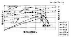
ここで、上記(1)式の温度・電流補償電圧VRの妥当性について、図2,図3により説明する。図2は光の強度が変化した場合で、光の強度が小さくなるに従い太陽電池電力Psが減少するため、最大電力点は太陽電池電流の下方向へ移動する。当然、太陽電池電圧VsもVs1からVs2へ変化する。この時、温度・電流補償電圧VRの一構成要素である電流補償電圧V2Rが電流Isの1次関数であるので、最適動作点追尾動作が実現できる。
【0012】
また、図3は太陽電池の動作温度が変化した場合で、動作温度が上昇するに伴い太陽電池電圧VsがVs1からVs2へ変化するが、最大電力点は太陽電池電流に対して変化しない。この時、温度・電流補償電圧VRの一構成要素である温度補償電圧V1Rは、動作温度に対してのみ電圧変化する要素であり、温度・電流補償電圧VRは動作温度の上昇によりVR-aからVR-bへ変化して、最適動作点追尾動作が実現できる。このように、最適動作点追尾動作の基準電圧を、温度・電流補償電圧VRとすることで、温度及び光量の変化に追随して太陽電池の最大電力点を与える電圧を追尾動作できるもので、外部環境変化に対応してより高精度の最適動作点追尾動作が可能となる。
【0013】
なお、温度・電流補償電圧VRを温度補償電圧V1Rのみで構成としても、ほぼ最大電力点で動作し最適動作点追尾は可能であるが、電流補償電圧V2Rを加えることでより高精度化を図ることができる。
また、前記(1)式中の増幅器#Aの増幅率K1は、太陽電池出力電流Is=0のときに、K1×VBを太陽電池出力電圧Vsの最小値であるVsmin に設定すればよく、また、増幅器#Bの増幅率K2は、太陽電池出力電圧Vsの最大値Vsmax と最小値Vsmin 、さらに太陽電池出力電流Isより与えられる導出式を(2),(3)に示す。
【0014】
【数2】
K1=Vsmin /VB ………(2)
K2=(Vsmax −Vsmin )/(Rm×Is) ………(3)
【0015】
次に、上記で得られた温度・電流補償電圧VRは、一方に太陽電池出力電圧Vsの入力された増幅器#Dの他方に入力され、太陽電池出力電圧Vsを温度・電流補償電圧VRに制御するよう動作し、増幅器#Dの出力にはそれに必要な制御信号ΔVRが現れる。そして、この制御信号ΔVRと、DC−DCコンバータ1の出力Eoに接続された負荷Rの出力電圧を電圧検出器#Eで検出し、DC−DCコンバータ1を定電圧制御する制御信号ΔVo、言い換えればスイッチング電源の出力を安定制御するための制御信号と、を比較して閾値を設定し、この閾値と鋸歯状(三角)波発振器OSCの出力とを比較して、パルス幅変調比較器#Fの出力にパルス幅変調用の出力パルス波形が得られ、このパルスを出力することによりDC−DCコンバータ1の制御用スイッチSを制御する。従って、太陽電池最適動作点追尾動作が行われると共に、DC−DCコンバータ1の出力定電圧制御が行われる。
【0016】
次に、図4にDC−DCコンバータ1の動作時のコンバータ出力電流と出力電圧及び太陽電池電圧の関係から、DC−DCコンバータの出力定電圧制御領域と太陽電池最適動作点追尾動作領域の一例について示す。即ち、DC−DCコンバータ1の出力定電圧制御領域は出力電流0.2A以下の領域であり、DC−DCコンバータ1の出力電力Poと太陽電池SBの供給電力Psは、〔Po<Ps〕なる関係となる。従って、DC−DCコンバータ1の出力電圧Eoは安定化されるが、太陽電池最適動作点追尾動作は行われないため動作時の太陽電池電圧Vsは変化する。次に、太陽電池最適動作点追尾動作領域は、出力電流0.2A以上の領域となる。この領域では、〔Po>Ps〕なる関係となり、図4から明らかなように太陽電池電圧Vsは、最適動作点追尾動作により一定電圧に制御されることになり、この領域では常時、太陽電池SBの最大電力が得られる。
【0017】
また、太陽電池SBの設置場所の温度,光量変化によってDC−DCコンバータ1の出力電圧は安定化さない、いわゆる垂下状態となった場合は、DC−DCコンバータ1の出力Eoに蓄電池EBを接続すれば、蓄電池EB自身の持つ定電圧値によりコンバータ出力は安定化される。この場合、太陽電池SBの出力電力が負荷消費電力を上回る環境に変化したときは、太陽電池SBの最大電力を蓄電池EBに給電する充電器として構成できる。
また、図5に示すような2つの入力電源E1,E2と、それに対応するスイッチS1,S2、磁気結合するインダクタLの巻線N1,N2と出力用巻線N0により構成された2入力DC−DCコンバータにおいて、例えば、入力電源として、E1を太陽電池、E2を商用電源入力を整流することで得られる直流電源とし、太陽電池E1に本発明による最適動作点追尾動作を適用し、直流電源E2からの給電を太陽電池E1の給電不足分を補うように給電させることもできる。
【0018】
即ち、DC−DCコンバータ全体の負荷給電量と太陽電池E1の給電量の差分を直流電源E2から給電するように構成すれば、太陽電池E1は常に最適動作点追尾動作を行い、また、直流電源E2の作用によりDC−DCコンバータ出力は蓄電池なしで定電圧制御され、太陽電池最適動作点追尾と出力定電圧制御が同時に実現でき、高効率でしかも安定なものとなる。
更に、パルス幅変調比較器#Fを有しない自励型フライバックタイプ等のDC−DCコンバータの場合には、出力定電圧制御信号ΔVoを出力する制御回路に、前記制御信号ΔVRを入力することで実現可能である。
また、前述した実施例は、スイッチング電源をDC−DCコンバータを用いた例で説明したが、スイッチング電源としてDC−ACインバータを用いる場合にも本発明を適用することができる。
【0019】
次に、太陽電池を用いた電源装置においては、光の照射が確実に行われている昼間と、光の照射が殆ど行われない夜間との変り目である朝,夕等の光量が著しく変化する場合の問題と、その改善策について説明する。
前述した電源装置の太陽電池最適動作点追尾回路の基本原理としては、太陽電池の外部環境(温度,光量)変化に伴う動作電圧を、太陽電池の温度特性と略同一のPN接合ダイオードの順方向降下電圧による温度補償電圧、又は光量の変化による太陽電池の出力電流の変化を電流補償電圧として検出し、この変化量をスイッチング電源の制御駆動用スイッチのPWMに関係させて制御するようにしているものであり、この制御に必要な制御量をスイッチング電源の制御用スイッチにパルス信号の形で与えている。
【0020】
従って、太陽電池の検出する電圧が温度補償電圧又は温度・電流補償電圧(基準電圧)と比較し高いほど制御用スイッチのパルス幅は広がり、基準電圧に近づくほどパルス幅は狭くなる。また、夜間等の太陽電池の検出する電圧が基準電圧を下回る時間帯は、制御用スイッチへの制御パルスは発生せずに、太陽電池の使用は禁止される。
この時、問題となるのは、光の照射量(光量)が極端に減少する、例えば、朝,夕等の時間帯である。この時間帯においては、夜間と昼間の2つの時間帯の動作、つまり制御用スイッチの動作はパルス発生−停止という状態をランダムに繰り返される。そして、このパルスのランダム発生により電源装置から不快な動作音やノイズが発生し、電源装置は不安定動作を繰り返す。
【0021】
このランダム動作は、図6に示すように太陽電池の特性から生じ、太陽電池を電源装置の入力源として使用する際には避けられない特性である。即ち、朝,夕のような若干の照射がある時の太陽電池は、電池出力電流Isが零の場合には、自身の出力電圧Vsは開放電圧まで上昇する。従って、基準電圧より高いために見掛上では太陽電池の使用は可能な状態にある。しかし、電流を給電し始めると、通常動作時に比較して急激に電圧が低下してしまうため、基準電圧より低くなり太陽電池の使用は不可能な状態にある。従って、このような状況で太陽電池をスイッチング電源の入力源として接続すれば、当然、上記のようなランダム動作となってしまう。
【0022】
そこで、照射量が極端に減少した場合には、スイッチング電源を別に設定する長い周期で動作−停止の繰り返しを行う太陽電池の動作状態検出回路を提供するもので、図7に動作状態検出回路の一実施例を示すと共に、制御タイムチャートを図8に示し、その回路動作を説明する。
フリップフロップ#IのCKに入力されるスイッチング電源の制御スイッチ信号である図8(a)のPWM出力のLエッジ(スイッチOFF命令)によりフリップフロップ#Iの出力バーQ(図8(c))はLとなり、抵抗R1 、コンデンサC1 の時定数からなる周期設定用のタイマー回路#Mを起動する。そして徐々に上昇する図8(b)のコンデンサC1 の電圧Vcと、例えば、抵抗R2 ,R3 の分圧等で構成された零電圧付近の零電圧基準電圧Vref0を比較器#Kにて比較し、Vc>Vref0なる期間にフリップフロップ#IのCLをLとして、フリップフロップ#Iの出力バーQをHに固定する。この状態は、タイマー回路#Mが設定周期によりリセットするまで継続しこの間フリップフロップ#IはCK入力を受け付けない。
【0023】
また、同時に先のPWM出力のLエッジ(スイッチOFF命令)により生じたフリップフロップ#Iの出力バーQ(図8(c))のL信号はフリップフロップ#HのCKに入力され、太陽電池電圧Vsと温度補償電圧V1Rの2つの入力により構成される比較器#Gの図8(d)に示す出力が、同図左側に示すようにHの時には太陽電池SBを使用停止として、フリップフロップ#Hの出力バーQ(図8(e))をLとし、更にアンド回路#Lの一方の入力をLとする。このアンド回路#Lの他方の入力にはPWM出力信号が入力されるが、太陽電池が使用不能状態の際には、PWMに同期する制御用スイッチSの制御信号であるアンド回路#Lの信号Psw(図8(f))をLとし、スイッチング電源を停止状態とする。
【0024】
同様に、図8の右側に示すように比較器#G出力の図8(d)がLの時にはフリップフロップ#Hの出力バーQ(図8(e))はHとなり、アンド回路#L出力はPWM出力に同期した制御パルスPsw(図8(f))を制御用駆動スイッチSに与えることになる。従って、上記のように照射量が極端に減少する時の太陽電池の動作状態検出は、設定するタイマー#Mの動作周期に同期して行われ、スイッチング電源の動作も常に一定周期となるため、例えば、タイマー#Mの動作を1secに設定したとすれば、周波数は1Hzとなり可聴音とならず、ノイズ的に低周波数であり問題とならない。
この太陽電池状態検出機能を盛り込んだ電源装置の太陽電池最適動作点追尾回路の構成例を図9に示してある。
【0025】
【発明の効果】
本発明は、以上詳細に説明したように太陽電池をスイッチング電源の直流入力電源として使用する際、温度補償や電流補償を考慮した電源装置の太陽電池最適動作点追尾回路であるので、太陽電池設置場所の環境変化による太陽電池の動作温度や光の強度に対しても、スイッチング電源の出力電力が太陽電池の供給電力を上回る場合には太陽電池の最大電力が得られ、また、スイッチング電源の出力電力が太陽電池の供給電力を下回る場合にはスイッチング電源の出力電圧を安定化できる。
【図面の簡単な説明】
【図1】本発明の太陽電池最適動作点追尾回路の一実施例を用いた電源装置のブロック回路図である。
【図2】太陽電池の光量変化による出力電流,電圧,電力特性と最適動作点追尾基準電圧との関係を示す特性図である。
【図3】太陽電池の温度変化による出力電流,電圧,電力特性と最適動作点追尾基準電圧との関係を示す特性図である。
【図4】本発明におけるDC−DCコンバータの出力定電圧制御領域と太陽電池最適動作点追尾動作領域を示す特性図である。
【図5】本発明を2入力コンバータに適用する場合の簡略した回路図である。
【図6】太陽電池の光量減少時の出力電流と出力電圧の関係を示す特性図である。
【図7】本発明の太陽電池最適動作点追尾回路に付加して用いる太陽電池の動作状態検出回路の一実施例ブロック回路図である。
【図8】本発明に係る太陽電池の動作状態検出回路の動作を示す制御タイムチャートである。
【図9】本発明の太陽電池最適動作点追尾回路に動作状態検出回路を適用した全体的ブロック回路図である。
【符号の説明】
1 DC−DCコンバータ
SB 太陽電池
Rm 電流検出器
Icon 定電流給電回路
D0-1 ,D0-2 〜D0-n PN接合ダイオード
VD PN接合ダイオードDの順方向降下電圧
VB PN接合ダイオードn個を縦続接続したときの順方向降下電圧
#A,#B 増幅器
#C 加算器
#D 差動増幅器
#E 電圧検出器
#F パルス幅変調比較器
#G,#K 比較器
#H,#I フリップフロップ
#J ノット回路
#L アンド回路
#M タイマー
V1R 温度補償電圧
V2R 電流補償電圧
VR 温度・電流補償電圧
Is 太陽電池出力電流
Vs 太陽電池出力電圧
ΔVR,ΔVo 制御信号
Eo DC−DCコンバータ出力電圧
R 負荷
OSC 鋸歯状波発振器
PWM パルス幅変調信号
S DC−DCコンバータの制御用駆動スイッチ
E1 ,E2 入力電源
D1 ,D2 ,D3 ダイオード
S1 ,S2 スイッチ
L インダクタ
N1 ,N2 一次巻線
N3 出力巻線
Vc コンデンサ電圧
Vref0 零電圧基準電圧
EB 蓄電池[0001]
BACKGROUND OF THE INVENTION
The present invention relates to a power supply device that obtains required power from a solar battery using a switching power supply, and in particular, changes in the external environment of the place where the solar battery is installed, that is, changes in temperature, light intensity (light quantity), etc. The present invention also relates to a solar cell optimum operating point tracking circuit of a power supply device that can always supply the maximum output power from the solar cell.
[0002]
[Prior art]
The solar cell optimum operating point tracking circuit of the conventional power supply device that takes out as much power as possible according to the intensity of light from the solar cell, the output voltage of the solar cell connected as the input power supply when the power supply device operates, An arbitrary fixed voltage predicted so as to obtain the maximum output in advance is set, and the output current is taken out from the solar cell, and power is fed through the switching power supply.
[0003]
[Problems to be solved by the invention]
However, the optimum operating point tracking circuit in which the output voltage of the solar cell connected to the switching power supply is predicted to be the maximum output in advance and set to an arbitrary fixed voltage has the following problems. In other words, the operating temperature of the solar cell changes during the day due to morning, noon, night, sunny days and rainy days, and seasonal changes such as summer and winter. When the optimum operating point is given, the output voltage of the solar cell rises when the operating temperature is lowered, so that there is a problem that the maximum output power corresponding to the operating temperature change cannot be obtained. Also, when the light intensity (light quantity) changes, as with the change in operating temperature, if the optimum operating point is given when the light quantity is high, the maximum current capacity can be supplied when the light quantity is high, but the light quantity is low. In this case, only a current capacity smaller than the maximum current capacity can be obtained, and there is a problem that the maximum output power cannot be obtained following the change in the light amount.
[0004]
As described above, in the optimum operating point tracking circuit in which the output voltage of the solar cell connected to the switching power supply is set to an arbitrary fixed voltage in advance, the change in the operating temperature and the amount of light due to the environmental change in the solar cell installation location causes the solar cell to It is difficult to supply maximum power. In the present invention,the maximum power of the solar cell can be obtained when the output power of theswitching power supply exceeds the supply power of the solar cell , even when the operating temperature and the amount of light change due to the change in the external environment of the solar cell installation location.When the output power of the switching power supply is lower than the power supplied by the solar battery, the output voltage of the switching power supply can be stabilized.
[0005]
The solar cell optimum operating point tracking circuit in the power source device using the solar cell of the present invention is a power source device including a switching power source circuit that receives the power of the solar cell, and is provided in the vicinity of the solar cell. A temperature compensated voltage detection circuit for supplying a current to a PN junction diode having substantially the same temperature characteristic as the temperature characteristic to detect a forward voltage drop of the PN junction diode; and the solar cell in accordance with the amount of light at the solar cell installation location A current detector for detecting a solar cell output current flowing from the power supply circuit to the switching power supply circuit, a first amplifier for amplifying the forward drop voltage with a first required amplification factor and outputting a temperature compensation voltage, and the solar cell A second amplifier that outputs a current compensation voltage by amplifying a voltage corresponding to the output current at a second required amplification factor; and the temperature compensation voltage and the current compensation voltage. San, said adder for outputting a temperature-current compensation voltage which is a linear sum of a voltage corresponding to the forward voltage drop between the solar cell output current,a solar cell output said is the output voltage from the solar cellA voltage is input to one side, the temperature / current compensation voltage is input to the other, and a differential amplifier that outputs a first control signal and a voltage of a load connected to the output side of the switching power supply circuit are detected. A voltage detector that outputs a second control signal for constant voltage control, and a pulse width modulation comparator that generates a pulse waveform for pulse width modulation control of the control switch of the switching power supply circuit. A modulation comparator compares either the first control signal or the second control signal with an output signal from a triangular wave generator to generate the pulse waveform, thereby generating a pulse waveform from the solar cell. When the magnitude of the force exceeds the magnitude of power output from the switching power supply circuit to the load, the voltage of the switching power supply circuit is stabilized, and the magnitude of power from the solar cell is the switching power supply circuit. When the power output from the solar cell is below the magnitude of the power, the power obtained from the solar cell is maximized, the temperature compensation voltage is compared with the output voltage of the solar cell every predetermined time, and the solar cell When the output voltage falls below the temperature compensation voltage, the switching power supply is stopped, and when the output voltage of the solar cell exceeds the temperature compensation voltage, the control switch for the switching power supply is controlled by the pulse width modulation control. The control is performed by the drive signal.
[0007]
DETAILED DESCRIPTION OF THE INVENTION
FIG. 1 shows an embodiment of a solar cell optimum operating point tracking circuit according to the present invention, which is shown as an example in which a DC-DC converter is used as a switching power source connected to the solar cell. In FIG. 1, 1 is a DC-DC converter, SB is a solar cell connected to the input of the DC-
[0008]
Each of #A and #B is an amplifier, and amplifier #A amplifies the forward voltage drop of one or a plurality of PN junction diodes D connected in cascade to a required temperature compensation voltage V1R. The amplifier #B detects the output current of the solar cell SB based on the intensity of the irradiated light, that is, the light amount as a voltage value, and amplifies it to a required current (light amount) compensation voltage V2R. #C is an adder for adding the temperature compensation voltage V1R and the current compensation voltage V2R. #D is a differential amplifier, which receives the temperature / current compensation voltage (reference voltage) VR output from the adder #C and the output voltage Vs of the solar battery SB, and outputs a control signal ΔVR. R is a load connected to the output of the DC-
[0009]
Next, FIG. 1 is a circuit diagram of an embodiment of the present invention, the output current, voltage, and power characteristics of the solar cell SB based on the change in the amount of light in FIG. , The power characteristic diagram, and the solar cell optimum of the present invention based on the current, voltage, and power characteristic diagram showing the relationship between the output constant voltage control region of the DC-
First, in the solar cell optimum operating point tracking circuit of FIG. 1, n PN junction diodes D having a forward voltage drop VD are connected in cascade, and a constant current is supplied thereto by passing a constant current from a constant current feeder circuit Icon. The direction drop voltage VB (VD × n) is amplified K1 times by the amplifier #A, and this is supplied to one of the adders #C as the temperature compensation voltage V1R (VB × K1). Further, the output current Is of the solar cell SB during the operation of the DC-
[0010]
Therefore, the temperature / current compensation voltage VR appearing at the output of the adder #C is
[Expression 1]
VR = V1R + V2R = VB × K1 + Is × Rm × K2 (1)
And is given in the form of a sum of a temperature compensation voltage V1R that changes only with temperature and a current compensation voltage V2R that is a linear function of the current that changes with respect to the current based on the change in the amount of light.
Here, the validity of the temperature / current compensation voltage VR in the equation (1) will be described with reference to FIGS. FIG. 2 shows the case where the light intensity changes. Since the solar cell power Ps decreases as the light intensity decreases, the maximum power point moves downward in the solar cell current. Naturally, the solar cell voltage Vs also changes from Vs1 to Vs2. At this time, since the current compensation voltage V2R, which is one component of the temperature / current compensation voltage VR, is a linear function of the current Is, the optimum operation point tracking operation can be realized.
[0012]
FIG. 3 shows a case where the operating temperature of the solar cell changes. As the operating temperature rises, the solar cell voltage Vs changes from Vs1 to Vs2, but the maximum power point does not change with respect to the solar cell current. At this time, the temperature compensation voltage V1R, which is a component of the temperature / current compensation voltage VR, is an element that changes only with respect to the operating temperature, and the temperature / current compensation voltage VR changes from VR-a as the operating temperature increases. By changing to VR-b, the optimum operation point tracking operation can be realized. Thus, by setting the reference voltage of the optimum operating point tracking operation as the temperature / current compensation voltage VR, the voltage that gives the maximum power point of the solar cell following the change in temperature and light quantity can be tracked, In response to changes in the external environment, it is possible to perform the optimum operation point tracking operation with higher accuracy.
[0013]
Note that even if the temperature / current compensation voltage VR is configured only by the temperature compensation voltage V1R, it can operate at almost the maximum power point and the optimum operating point can be tracked. However, by adding the current compensation voltage V2R, higher accuracy is achieved. be able to.
Further, the amplification factor K1 of the amplifier #A in the equation (1) may be set such that K1 × VB is set to Vsmin that is the minimum value of the solar cell output voltage Vs when the solar cell output current Is = 0. The amplification factor K2 of the amplifier #B is derived from the maximum value Vsmax and the minimum value Vsmin of the solar cell output voltage Vs and the derivation formulas given by the solar cell output current Is in (2) and (3).
[0014]
[Expression 2]
K1 = Vsmin / VB (2)
K2 = (Vsmax−Vsmin) / (Rm × Is) (3)
[0015]
Next, the temperature / current compensation voltage VR obtained above is input to the other side of the amplifier #D to which the solar cell output voltage Vs is input, and the solar cell output voltage Vs is controlled to the temperature / current compensation voltage VR. The necessary control signal ΔVR appears at the output of the amplifier #D. Then, this control signal ΔVR and the output voltage of the load R connected to the output Eo of the DC-
[0016]
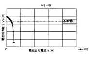
Next, FIG. 4 shows an example of the output constant voltage control region and the solar cell optimum operation point tracking operation region of the DC-DC converter based on the relationship between the converter output current, the output voltage, and the solar cell voltage when the DC-
[0017]
In addition, when the output voltage of the DC-
Further, the two input power sources E1 and E2 as shown in FIG. 5, the corresponding switches S1 and S2, the windings N1 and N2 of the inductor L to be magnetically coupled, and the output winding N0, and the two-input DC− In the DC converter, for example, as an input power supply, E1 is a solar battery, E2 is a DC power supply obtained by rectifying a commercial power supply input, the optimum operating point tracking operation according to the present invention is applied to the solar battery E1, and the DC power supply E2 Can be fed so as to make up for the lack of feeding of the solar cell E1.
[0018]
In other words, if the DC power supply is configured so that the difference between the load power supply amount of the entire DC-DC converter and the power supply amount of the solar battery E1 is supplied from the DC power supply E2, the solar battery E1 always performs the optimum operating point tracking operation, and the DC power supply. Due to the action of E2, the DC-DC converter output is controlled at a constant voltage without a storage battery, and the solar cell optimum operating point tracking and the output constant voltage control can be realized at the same time, resulting in high efficiency and stability.
Further, in the case of a DC-DC converter such as a self-excited flyback type that does not have a pulse width modulation comparator #F, the control signal ΔVR is input to a control circuit that outputs an output constant voltage control signal ΔVo. It is feasible.
Moreover, although the Example mentioned above demonstrated the example using a DC-DC converter as a switching power supply, this invention is applicable also when using a DC-AC inverter as a switching power supply.
[0019]
Next, in a power supply device using a solar cell, the amount of light in the morning, evening, etc., which is a transition between the daytime when light irradiation is reliably performed and the nighttime when light irradiation is hardly performed, changes significantly. Explain the problem and how to improve it.
The basic principle of the solar cell optimum operating point tracking circuit of the power supply device described above is that the operating voltage accompanying the change in the external environment (temperature, light quantity) of the solar cell is the forward direction of the PN junction diode substantially the same as the temperature characteristic of the solar cell. A change in the temperature compensation voltage due to the drop voltage or a change in the output current of the solar cell due to a change in the amount of light is detected as a current compensation voltage, and this change is controlled in relation to the PWM of the control drive switch of the switching power supply. The control amount necessary for this control is given to the control switch of the switching power supply in the form of a pulse signal.
[0020]
Accordingly, the higher the voltage detected by the solar cell is compared with the temperature compensation voltage or the temperature / current compensation voltage (reference voltage), the wider the pulse width of the control switch, and the closer the reference voltage, the narrower the pulse width. In addition, during the time period when the voltage detected by the solar cell is lower than the reference voltage, such as at night, the use of the solar cell is prohibited without generating a control pulse to the control switch.
At this time, the problem is a time zone such as morning and evening when the amount of light irradiation (light quantity) is extremely reduced. In this time zone, the operation in two time zones, nighttime and daytime, that is, the operation of the control switch, is repeated at random in the state of pulse generation-stop. The random generation of pulses causes unpleasant operation noise and noise from the power supply device, and the power supply device repeats unstable operation.
[0021]
This random operation is caused by the characteristics of the solar cell as shown in FIG. 6, and is an unavoidable characteristic when the solar cell is used as an input source of the power supply device. That is, when there is a slight amount of irradiation such as morning and evening, when the battery output current Is is zero, its own output voltage Vs rises to the open circuit voltage. Therefore, since it is higher than the reference voltage, the solar cell is apparently usable. However, when the current starts to be fed, the voltage is drastically decreased as compared with the normal operation, so that the voltage becomes lower than the reference voltage and the use of the solar cell is impossible. Therefore, if a solar cell is connected as an input source of a switching power supply in such a situation, naturally the above random operation is performed.
[0022]
Therefore, when the irradiation amount is extremely reduced, an operation state detection circuit for a solar cell that repeats operation-stop in a long cycle in which a switching power supply is set separately is provided. FIG. While showing one Example, a control time chart is shown in FIG. 8, and the circuit operation | movement is demonstrated.
The output bar Q of the flip-flop #I (FIG. 8 (c)) by the L edge (switch OFF command) of the PWM output of FIG. 8 (a) which is the control switch signal of the switching power supply input to the CK of the flip-flop #I Becomes L, and starts a timer circuit #M for setting a cycle consisting of a time constant of the resistor R1 and the capacitor C1. Then, the voltage Vc of the capacitor C1 in FIG. 8 (b), which gradually increases, is compared with the zero voltage reference voltage Vref0 in the vicinity of the zero voltage constituted by, for example, the divided voltages of the resistors R2 and R3 by the comparator #K. , The CL of the flip-flop #I is set to L during the period of Vc> Vref0, and the output bar Q of the flip-flop #I is fixed to H. This state continues until the timer circuit #M is reset at the set cycle, and during this time, the flip-flop #I does not accept the CK input.
[0023]
At the same time, the L signal of the output bar Q (FIG. 8 (c)) of the flip-flop #I generated by the L edge (switch OFF command) of the previous PWM output is input to the CK of the flip-flop #H, and the solar cell voltage When the output shown in FIG. 8D of the comparator #G constituted by two inputs of Vs and the temperature compensation voltage V1R is H as shown on the left side of the figure, the use of the solar cell SB is stopped, and the flip-flop # The output bar Q of H (FIG. 8E) is set to L, and one input of the AND circuit #L is set to L. A PWM output signal is input to the other input of the AND circuit #L. When the solar cell is in an unusable state, a signal of the AND circuit #L that is a control signal of the control switch S synchronized with PWM. Psw (FIG. 8 (f)) is set to L, and the switching power supply is stopped.
[0024]
Similarly, as shown on the right side of FIG. 8, when the output of the comparator #G shown in FIG. 8 (d) is L, the output bar Q (FIG. 8 (e)) of the flip-flop #H becomes H, and the AND circuit #L output Gives a control pulse Psw (FIG. 8 (f)) synchronized with the PWM output to the control drive switch S. Therefore, the operation state detection of the solar cell when the irradiation amount is extremely reduced as described above is performed in synchronization with the operation cycle of the timer #M to be set, and the operation of the switching power supply is always in a constant cycle. For example, if the operation of the timer #M is set to 1 sec, the frequency is 1 Hz and the sound is not audible, and the noise is low and there is no problem.
FIG. 9 shows a configuration example of the solar cell optimum operating point tracking circuit of the power supply device incorporating this solar cell state detection function.
[0025]
【The invention's effect】
Since the present invention is a solar cell optimum operating point tracking circuit of a power supply device considering temperature compensation and current compensation when using a solar cell as a DC input power source of a switching power source as described in detail above, the solar cell installation Whenthe output power of theswitching power supply exceeds the supply power of the solar battery, the maximum power of the solar battery can be obtained with respect to the operating temperature and light intensity of the solar battery due to the environmental change of the location.When the power is lower than the power supplied by the solar cell, the output voltage of the switching power supply can be stabilized.
[Brief description of the drawings]
FIG. 1 is a block circuit diagram of a power supply device using one embodiment of a solar cell optimum operating point tracking circuit of the present invention.
FIG. 2 is a characteristic diagram showing the relationship between output current, voltage, and power characteristics due to changes in the amount of light of a solar cell and an optimum operating point tracking reference voltage.
FIG. 3 is a characteristic diagram showing a relationship between output current, voltage, and power characteristics due to a temperature change of a solar cell and an optimum operating point tracking reference voltage.
FIG. 4 is a characteristic diagram showing an output constant voltage control region and a solar cell optimum operation point tracking operation region of the DC-DC converter according to the present invention.
FIG. 5 is a simplified circuit diagram when the present invention is applied to a two-input converter.
FIG. 6 is a characteristic diagram showing the relationship between the output current and the output voltage when the amount of light of the solar cell is reduced.
FIG. 7 is a block circuit diagram of an embodiment of a solar cell operating state detection circuit used in addition to the solar cell optimum operating point tracking circuit of the present invention.
FIG. 8 is a control time chart showing the operation of the operation state detection circuit of the solar cell according to the present invention.
FIG. 9 is an overall block circuit diagram in which an operation state detection circuit is applied to the solar cell optimum operation point tracking circuit of the present invention.
[Explanation of symbols]
1 DC-DC converter SB Solar cell Rm Current detector Icon Constant current feed circuit D0-1, D0-2 to D0-n PN junction diode VD Forward drop voltage VB of PN junction diode D VB PN junction diode n cascaded Forward voltage drop #A, #B amplifier #C adder #D differential amplifier #E voltage detector #F pulse width modulation comparator #G, #K comparator #H, #I flip-flop #J Not circuit #L AND circuit #M Timer V1R Temperature compensation voltage V2R Current compensation voltage VR Temperature / current compensation voltage Is Solar cell output current Vs Solar cell output voltage ΔVR, ΔVo control signal Eo DC-DC converter output voltage R Load OSC Sawtooth Wave oscillator PWM pulse width modulation signal S DC-DC converter control drive switches E1, E2 Input power supplies D1, D2, D3 Diodes S1,
Claims (2)
Translated fromJapanese前記太陽電池の近傍に設けられ、前記太陽電池の温度特性と略同じ温度特性を有するPN接合ダイオードに電流を給電して該PN接合ダイオードの順方向降下電圧を検出する温度補償電圧検出回路と、
前記太陽電池設置場所の光量に応じて前記太陽電池から前記スイッチング電源回路に流れる太陽電池出力電流を検出する電流検出器と、
前記順方向降下電圧を第1の所要増幅率で増幅して温度補償電圧を出力する第1の増幅器と、
前記太陽電池出力電流に応じた電圧を第2の所要増幅率で増幅して電流補償電圧を出力する第2の増幅器と、
前記温度補償電圧と前記電流補償電圧とを加算して、前記前記順方向降下電圧と前記太陽電池出力電流に応じた電圧との線形和である温度・電流補償電圧を出力する加算器と、
前記太陽電池からの出力電圧である太陽電池出力電圧が一方に入力され、前記温度・電流補償電圧が他方に入力されて、第1の制御信号を出力する差動増幅器と、
前記スイッチング電源回路の出力側に接続された負荷の電圧を検出して定電圧制御する第2の制御信号を出力する電圧検出器と、
前記スイッチング電源回路の制御用スイッチをパルス幅変調制御するパルス波形を発生するパルス幅変調比較器と、を備え、
前記パルス幅変調比較器は、
前記第1の制御信号または前記第2の制御信号のいずれかを三角波発信器からの出力信号と比較することによって前記パルス波形を発生して、
前記太陽電池からの電力の大きさが、前記スイッチング電源回路から負荷に出力される電力の大きさを上回ったときには、前記スイッチング電源回路の電圧を安定とし、
前記太陽電池からの電力の大きさが、前記スイッチング電源回路から負荷に出力される電力の大きさを下回ったときには、前記太陽電池から得られる電力を最大とし、
前記温度補償電圧と前記太陽電池の出力電圧とを所定時間毎に比較し、前記太陽電池の出力電圧が前記温度補償電圧を下回ったとき、前記スイッチング電源を停止状態とせしめ、
前記太陽電池の出力電圧が前記温度補償電圧を上回ったとき、前記スイッチング電源の制御用スイッチを前記パルス幅変調制御する前記駆動信号によって制御せしめるようにする、太陽電池を用いた電源装置における太陽電池最適動作点追尾回路。In a power supply device composed of a switching power supply circuit that uses solar cell power as input,
A temperature compensated voltage detection circuit that is provided in the vicinity of the solar cell and supplies a current to a PN junction diode having substantially the same temperature characteristics as the temperature characteristic of the solar cell to detect a forward voltage drop of the PN junction diode;
A current detector for detecting a solar cell output current flowing from the solar cell to the switching power supply circuit according to the amount of light at the solar cell installation location;
A first amplifier that amplifies the forward drop voltage with a first required gain and outputs a temperature compensated voltage;
A second amplifier for amplifying a voltage corresponding to the solar cell output current with a second required amplification factor and outputting a current compensation voltage;
An adder that adds the temperature compensation voltage and the current compensation voltage, and outputs a temperature / current compensation voltage that is a linear sum of the forward drop voltage and a voltage corresponding to the solar cell output current;
A differential amplifier that outputs a first control signal when asolar cell output voltage, which is an output voltage from the solar cell, is input to one side, and the temperature / current compensation voltage is input to the other;
A voltage detector that outputs a second control signal for detecting a voltage of a load connected to the output side of the switching power supply circuit and performing constant voltage control;
A pulse width modulation comparator that generates a pulse waveform for pulse width modulation control of the control switch of the switching power supply circuit,
The pulse width modulation comparator is
Generating the pulse waveform by comparing either the first control signal or the second control signal with an output signal from a triangular wave transmitter;
When the magnitude of power from the solar cell exceeds the magnitude of power output from the switching power supply circuit to the load, the voltage of the switching power supply circuit is stabilized,
When the amount of power from the solar cell is less than the amount of power output from the switching power supply circuit to the load, the power obtained from the solar cell is maximized,
Comparing the temperature compensated voltage and the output voltage of the solar cell every predetermined time, and when the output voltage of the solar cell falls below the temperature compensated voltage, the switching power supply is stopped.
When the output voltage of the solar cell exceeds the temperature compensation voltage, the solar cell in the power supply apparatus using the solar cell is configuredto control the control switch of the switching power supply by the driving signal for pulse width modulation control. Optimal operating point tracking circuit.
Priority Applications (1)
| Application Number | Priority Date | Filing Date | Title |
|---|---|---|---|
| JP16277498AJP3949818B2 (en) | 1998-05-28 | 1998-05-28 | Solar cell optimum operating point tracking circuit in a power supply using solar cells |
Applications Claiming Priority (1)
| Application Number | Priority Date | Filing Date | Title |
|---|---|---|---|
| JP16277498AJP3949818B2 (en) | 1998-05-28 | 1998-05-28 | Solar cell optimum operating point tracking circuit in a power supply using solar cells |
Publications (3)
| Publication Number | Publication Date |
|---|---|
| JPH11341699A JPH11341699A (en) | 1999-12-10 |
| JPH11341699A5 JPH11341699A5 (en) | 2005-08-04 |
| JP3949818B2true JP3949818B2 (en) | 2007-07-25 |
Family
ID=15760975
Family Applications (1)
| Application Number | Title | Priority Date | Filing Date |
|---|---|---|---|
| JP16277498AExpired - Fee RelatedJP3949818B2 (en) | 1998-05-28 | 1998-05-28 | Solar cell optimum operating point tracking circuit in a power supply using solar cells |
Country Status (1)
| Country | Link |
|---|---|
| JP (1) | JP3949818B2 (en) |
Families Citing this family (7)
| Publication number | Priority date | Publication date | Assignee | Title |
|---|---|---|---|---|
| WO2005050813A1 (en) | 2003-11-19 | 2005-06-02 | Shindengen Electric Manufacturing Co.,Ltd. | Charger, and dc/dc converter having this charger |
| WO2005083868A1 (en) | 2004-02-27 | 2005-09-09 | Shindengen Electric Manufacturing Co., Ltd. | Charger, dc/dc converter having that charger, and control circuit thereof |
| TWI274454B (en) | 2005-03-04 | 2007-02-21 | Ind Tech Res Inst | A power management method and system of a hybrid power supply |
| JP4137175B2 (en) | 2005-05-12 | 2008-08-20 | 新電元工業株式会社 | DC-DC converter |
| CN102353458A (en)* | 2011-07-08 | 2012-02-15 | 凯迈(洛阳)测控有限公司 | Temperature signal acquisition circuit and application thereof, and infrared detector |
| CN107139769B (en)* | 2017-07-07 | 2023-08-08 | 深圳市皇驰科技有限公司 | Intelligent charging pile based on solar power supply |
| JP7734500B2 (en)* | 2021-03-30 | 2025-09-05 | Tdk株式会社 | Power conversion device and power storage system |
- 1998
- 1998-05-28JPJP16277498Apatent/JP3949818B2/ennot_activeExpired - Fee Related
Also Published As
| Publication number | Publication date |
|---|---|
| JPH11341699A (en) | 1999-12-10 |
Similar Documents
| Publication | Publication Date | Title |
|---|---|---|
| JP4725641B2 (en) | Buck-boost switching regulator | |
| JP3394996B2 (en) | Maximum power operating point tracking method and device | |
| US6429621B1 (en) | Solar power charging system | |
| KR101357006B1 (en) | Converter and the driving method thereof | |
| JPH1023686A (en) | Power supply using solar cells | |
| US20050110454A1 (en) | Methods and apparatuses for tracking maximum power point of solar electricity generating system | |
| US20070085519A1 (en) | Switching regulator with automatic multi mode conversion | |
| US5914591A (en) | Switching power supply | |
| US20110025283A1 (en) | Dc-dc converter, control circuit, and power supply control method | |
| CN109802556B (en) | Photovoltaic power generation system with photovoltaic inverter and starting method of inverter | |
| US20100263711A1 (en) | Maximum power point tracking control apparatus for solar battery | |
| US8837177B2 (en) | Electric generating system using solar cell | |
| JP3949818B2 (en) | Solar cell optimum operating point tracking circuit in a power supply using solar cells | |
| EP1187303B1 (en) | PWM Control circuit for DC-DC converter | |
| WO2015008456A1 (en) | Dc/dc converter | |
| JP3250979B2 (en) | Switching power supply | |
| JPH09261949A (en) | Dc/dc converter and solar generation system | |
| JP2007109609A (en) | Charging and discharging device of fuel cell system | |
| US20200267815A1 (en) | Battery-powered current regulator for pulsed loads | |
| Pernía et al. | A modular strategy for isolated photovoltaic systems based on microcontroller | |
| JP5721403B2 (en) | Buck-boost circuit and buck-boost circuit control method | |
| JP2003070242A (en) | Switching regulator | |
| JP3862320B2 (en) | Grid-connected inverter device | |
| JP2006014526A (en) | Power supply control method and power supply | |
| JPH1094266A (en) | Inverter device |
Legal Events
| Date | Code | Title | Description |
|---|---|---|---|
| A521 | Request for written amendment filed | Free format text:JAPANESE INTERMEDIATE CODE: A523 Effective date:20050113 | |
| A621 | Written request for application examination | Free format text:JAPANESE INTERMEDIATE CODE: A621 Effective date:20050113 | |
| A977 | Report on retrieval | Free format text:JAPANESE INTERMEDIATE CODE: A971007 Effective date:20060512 | |
| A131 | Notification of reasons for refusal | Free format text:JAPANESE INTERMEDIATE CODE: A131 Effective date:20060523 | |
| A521 | Request for written amendment filed | Free format text:JAPANESE INTERMEDIATE CODE: A523 Effective date:20060704 | |
| A02 | Decision of refusal | Free format text:JAPANESE INTERMEDIATE CODE: A02 Effective date:20061003 | |
| A521 | Request for written amendment filed | Free format text:JAPANESE INTERMEDIATE CODE: A821 Effective date:20061101 | |
| RD02 | Notification of acceptance of power of attorney | Free format text:JAPANESE INTERMEDIATE CODE: A7422 Effective date:20061101 | |
| A521 | Request for written amendment filed | Free format text:JAPANESE INTERMEDIATE CODE: A523 Effective date:20061129 | |
| A521 | Request for written amendment filed | Free format text:JAPANESE INTERMEDIATE CODE: A821 Effective date:20061102 | |
| A911 | Transfer to examiner for re-examination before appeal (zenchi) | Free format text:JAPANESE INTERMEDIATE CODE: A911 Effective date:20061207 | |
| A131 | Notification of reasons for refusal | Free format text:JAPANESE INTERMEDIATE CODE: A131 Effective date:20070320 | |
| A521 | Request for written amendment filed | Free format text:JAPANESE INTERMEDIATE CODE: A523 Effective date:20070327 | |
| TRDD | Decision of grant or rejection written | ||
| A01 | Written decision to grant a patent or to grant a registration (utility model) | Free format text:JAPANESE INTERMEDIATE CODE: A01 Effective date:20070417 | |
| A61 | First payment of annual fees (during grant procedure) | Free format text:JAPANESE INTERMEDIATE CODE: A61 Effective date:20070419 | |
| R150 | Certificate of patent or registration of utility model | Free format text:JAPANESE INTERMEDIATE CODE: R150 | |
| FPAY | Renewal fee payment (event date is renewal date of database) | Free format text:PAYMENT UNTIL: 20110427 Year of fee payment:4 | |
| FPAY | Renewal fee payment (event date is renewal date of database) | Free format text:PAYMENT UNTIL: 20120427 Year of fee payment:5 | |
| FPAY | Renewal fee payment (event date is renewal date of database) | Free format text:PAYMENT UNTIL: 20130427 Year of fee payment:6 | |
| FPAY | Renewal fee payment (event date is renewal date of database) | Free format text:PAYMENT UNTIL: 20130427 Year of fee payment:6 | |
| FPAY | Renewal fee payment (event date is renewal date of database) | Free format text:PAYMENT UNTIL: 20140427 Year of fee payment:7 | |
| R250 | Receipt of annual fees | Free format text:JAPANESE INTERMEDIATE CODE: R250 | |
| R250 | Receipt of annual fees | Free format text:JAPANESE INTERMEDIATE CODE: R250 | |
| R250 | Receipt of annual fees | Free format text:JAPANESE INTERMEDIATE CODE: R250 | |
| LAPS | Cancellation because of no payment of annual fees |