JP3944200B2 - Linear image sensor and image reading apparatus - Google Patents
Linear image sensor and image reading apparatusDownload PDFInfo
- Publication number
- JP3944200B2 JP3944200B2JP2004218824AJP2004218824AJP3944200B2JP 3944200 B2JP3944200 B2JP 3944200B2JP 2004218824 AJP2004218824 AJP 2004218824AJP 2004218824 AJP2004218824 AJP 2004218824AJP 3944200 B2JP3944200 B2JP 3944200B2
- Authority
- JP
- Japan
- Prior art keywords
- resolution
- image
- transfer
- transfer register
- image sensor
- Prior art date
- Legal status (The legal status is an assumption and is not a legal conclusion. Google has not performed a legal analysis and makes no representation as to the accuracy of the status listed.)
- Expired - Fee Related
Links
Images


Landscapes
- Facsimile Heads (AREA)
Description
Translated fromJapanese本発明はイメージセンサ、並びにイメージスキャナやファクシミリ、電子複写機等の画像読取装置等に用いられるイメージセンサに関するものである。 The present invention relates to an image sensor, and an image sensor used in an image reading apparatus such as an image scanner, a facsimile machine, and an electronic copying machine.
従来の画像読取装置において、解像度制御用のコントロール端子を設け、ユーザーが利用条件にあわせて解像度を切り替えることが可能な密着型イメージセンサが提案されている。(例えば、特許文献1参照)
図8は、特許文献1において提案されている密着型イメージセンサ用集積回路である。この従来技術においては、イメージセンサチップにコントロール端子を設け、その端子にユーザーがハイレベルまたはローレベルの信号を入力することにより高解像度モードと低解像度モードの解像度切り替えを実現している。
FIG. 8 shows an integrated circuit for a contact image sensor proposed in
しかしながら、上記従来の密着型イメージセンサの解像度切り替え方式においては、画素を読み飛ばすことにより解像度を切り替えているため、例えば転送クロックレートが同一の場合は、解像度を半分にしても読み出し時間は変わらない。従って、同一のクロックレートの転送クロックを用いて、解像度が1200dpi時は10[msec/line]の読取速度、解像度が600dpi時は5[msec/line]の読取速度というように、解像度に応じた適切な読取速度での読み取りを実現することができないという問題がある。 However, in the resolution switching method of the conventional contact-type image sensor, the resolution is switched by skipping the pixels. For example, when the transfer clock rate is the same, the reading time does not change even if the resolution is halved. . Therefore, using a transfer clock with the same clock rate, the reading speed is 10 [msec / line] when the resolution is 1200 dpi, and the reading speed is 5 [msec / line] when the resolution is 600 dpi. There is a problem that reading at an appropriate reading speed cannot be realized.
上記の問題を解決するために、本発明のリニアイメージセンサは、入射光を電荷に光電変換する複数の受光素子が配置された受光素子アレイと、前記受光素子アレイにおいて光電変換された電荷信号を第1の解像度で外部に転送する第1の転送レジスタと、前記受光素子アレイにおいて光電変換された電荷信号を前記第1の解像度の1/N(Nは自然数)である第2の解像度で外部に転送する第2の転送レジスタと、前記第1の転送レジスタ又は前記第2の転送レジスタのどちらを用いて前記電荷信号を外部に転送するのかを選択する選択手段とを有し、前記選択手段は、選択する転送レジスタに第1の周波数の転送クロックを供給し、選択しない転送レジスタに前記第1の周波数よりも低い第2の周波数のクロックを供給することを特徴とする。In order to solve the above problems, a linear image sensor of the present invention includes a light receiving element array in which a plurality of light receiving elements that photoelectrically convert incident light into electric charges, and a charge signal photoelectrically converted in the light receiving element array. A first transfer register for transferring to the outside at a first resolution; and a charge signal photoelectrically converted in the light receiving element array at an external at a second resolution that is 1 / N (N is a natural number) of the first resolution. second transfer register and,have a selecting means for selecting whether to transfer the charge signals to the outside using either of the first transfer register and the second transferregister, said selection means for transferring theincludes a feature toprovide a first supply transfer clock frequency, the clock of a second frequency lower than the first frequency to transfer registers not selected in the transfer register selects That.
本発明によれば、異なる読み取り解像度で画像を読み取る場合に、画質を劣化させることなく、読み取り解像度に応じた読取速度での画像読み取りを実現するとともに、無駄な電荷を外部に排出することができる。According to the present invention, when an image is read at a different reading resolution, image reading can be performed at a reading speed corresponding to the reading resolution without deteriorating image quality, and wasteful charges can bedischarged to the outside. .
(第1の実施形態)
以下、本発明の実施形態について、図面を用いて詳細に説明する。(First embodiment)
Hereinafter, embodiments of the present invention will be described in detail with reference to the drawings.
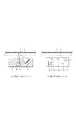
図1は、本実施形態に係る画像読取装置全体の構成概略図、図2は、本実施形態に係る画像読取装置におけるキャリッジの構成概略図、図3は、本実施形態に係る画像読取装置のブロック図である。以下にその構成について説明する。 1 is a schematic configuration diagram of the entire image reading apparatus according to the present embodiment, FIG. 2 is a schematic configuration diagram of a carriage in the image reading apparatus according to the present embodiment, and FIG. 3 is a diagram of the image reading apparatus according to the present embodiment. It is a block diagram. The configuration will be described below.
図1は、本実施形態に係る画像読取装置全体の構成概略図であり、(a)は一部切断平面図、(b)は一部切断正面図、(c)は側面説明図である。図1において、画像読取装置1の上面に取り付けられた原稿台ガラス2上に原稿をセットし、キャリッジ3内のイメージセンサにより短手方向の1次元の画像を読み取り、キャリッジ3をガイドシャフト4に沿って長手方向に解像度に応じた速度でモータ回路6によって移動させることにより、原稿に記載された2次元の画像を読み取る。 FIG. 1 is a schematic configuration diagram of the entire image reading apparatus according to the present embodiment, in which (a) is a partially cut plan view, (b) is a partially cut front view, and (c) is an explanatory side view. In FIG. 1, an original is set on an
図2は、本実施形態に係る画像読取装置におけるキャリッジ構成の概略図であり、(a)に示すような等倍光学系イメージセンサのキャリッジ、又は(b)に示すような縮小光学系イメージセンサのキャリッジが用いられる。 FIG. 2 is a schematic diagram of a carriage configuration in the image reading apparatus according to the present embodiment, and is a carriage of an equal-magnification optical system image sensor as shown in (a), or a reduction optical system image sensor as shown in (b). The carriage is used.
図2において、(a)に示す等倍光学系のキャリッジでは、光源8の照射光を原稿7が反射し、レンズ9を介してイメージセンサ10が受光することで、原稿7に記載された画像を読み取る。同様に、(b)に示す縮小光学系のキャリッジでは、光源8の照射光を原稿7が反射し、ミラー11_1〜11_3で屈折した光がレンズ9を介してイメージセンサ10に受光されることで、原稿7に記載された画像を読み取る。なお、反射原稿の読取について記載しているが、キャリッジの上部に別の光源を備えることで、透過原稿の読取も行うことができる。 In the carriage of the equal magnification optical system shown in FIG. 2A, the
図3は、本実施形態に係る画像読取装置の内部構成ブロック図である。外部装置18はホストコンピュータ等であり、画像読取装置1を制御するためのドライバを有しており、画像読取装置1と外部装置18は信号ケーブル等で接続されている。ドライバは、ユーザーによる解像度指定、読取範囲の指定、画像処理の指定等の画像読取モードを指定し、ユーザー指令に基づく外部装置18からの制御信号がインターフェイス15を介して、システムコントローラ17に入力される。システムコントローラ17は、外部装置18からの信号に基づいてモータ回路6、イメージセンサ10、点灯回路16等を作動させる。モータ回路6は、解像度に応じた速度でキャリッジ3をガイドシャフト4に沿って長手方向に移動させる回路であり、点灯回路16は、イメージセンサ10と同期して、原稿を照射する光源8を点灯させるための回路である。光源8から照射された光は原稿に反射され、レンズによってイメージセンサ10上に結像される。イメージセンサ10は結像された光を光電変換し、読取画像に応じたアナログ電気信号を出力する。AFE12は、イメージセンサ10から出力されたアナログ画像信号にアンプ増幅、A/D変換等の処理を行ない、デジタル画像信号を出力する。シェーディング補正回路13は、システムコントローラ17に記憶されている基準レベルの補正データに基づいて、AFE12から出力されたデジタル画像信号にシェーディング補正を行う。画像処理回路14は、シェーディング補正されたデジタル画像信号に対して、カラーバランス調整、ガンマ補正等と、外部装置18のドライバが指定した画像処理を行う。各種画像処理を施された画像データはインターフェイスを介して、外部装置18に出力され、外部装置18に接続してあるモニタやプリンタ等を介して画像を確認することができる。 FIG. 3 is an internal configuration block diagram of the image reading apparatus according to the present embodiment. The external device 18 is a host computer or the like, and has a driver for controlling the
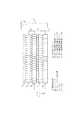
図4は、本実施形態の画像読取装置におけるイメージセンサ10の構成概略図である。 FIG. 4 is a schematic configuration diagram of the
本実施形態のイメージセンサは、第1の解像度で読み取りを行うための第1の転送レジスタ26と、第1の解像度よりも低解像度である第2の解像度で読み取りを行うための第2の転送レジスタ28を備え、指定された解像度に応じて2つの転送レジスタを使い分けるように構成されている。例えば、第1の解像度を1200dpiとした場合、第2の解像度としては第1の解像度の1/2の解像度である600dpiを設定可能である。 The image sensor according to the present embodiment includes a
なお、第2の解像度は、第1の解像度の1/N(Nは自然数)の解像度を設定すればよく、例えば、第1の解像度が4800dpi、第2の解像度が1200dpiであるようなN=4の解像度も設定することができる。この場合、第2の解像度では、第1の解像度のN画素を加算した画像信号を出力するため、間引き等による画像の不連続性を防止することができる。 Note that the second resolution may be set to 1 / N (N is a natural number) of the first resolution. For example, the first resolution is 4800 dpi and the second resolution is 1200 dpi. A resolution of 4 can also be set. In this case, in the second resolution, an image signal obtained by adding N pixels of the first resolution is output, so that image discontinuity due to thinning or the like can be prevented.
また、解像度は2種類に限らず3種類以上を設定することもできる。例えば、第1の解像度が4800dpi、第2の解像度が1200dpi、第3の解像度が300dpiであるような構成にすることもできる。この場合、第2の解像度では4画素分を加算して1画素として出力し、第3の解像度では16画素分を加算して1画素として出力する。 Further, the resolution is not limited to two types, and three or more types can be set. For example, the first resolution may be 4800 dpi, the second resolution may be 1200 dpi, and the third resolution may be 300 dpi. In this case, four pixels are added and output as one pixel in the second resolution, and 16 pixels are added and output as one pixel in the third resolution.
転送クロックパルス生成部21は、受光素子アレイ24において光電変換された電荷を転送レジスタ26及び28のそれぞれに転送して外部に画像信号として出力するためのクロックパルスCLK1及びCLK2を生成する。そして、転送クロックパルス生成部21は、ドライバにより指定された解像度を示す解像度信号19に応じて、クロックパルスCLK1又はCLK2のいずれかを生成し、第1の転送レジスタ26、第2の転送レジスタ28のどちらを使用して電荷信号を外部に出力するのかを選択する。 The transfer clock pulse generator 21 generates clock pulses CLK1 and CLK2 for transferring the charges photoelectrically converted in the light receiving element array 24 to the
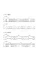
図5は、本実施形態のクロックパルスCLK1及びCLK2の波形図である。図5の(a)は第1の解像度で画像を読み取る場合のクロックパルスCLK1、(b)は第2の解像度で画像を読み取る場合のクロックパルスCLK2であり、解像度に応じてクロック生成部により異なるクロックパルスを生成して供給することで、解像度に応じた読取速度での画像読取を実現することができる。 FIG. 5 is a waveform diagram of the clock pulses CLK1 and CLK2 of the present embodiment. 5A is a clock pulse CLK1 when an image is read at the first resolution, and FIG. 5B is a clock pulse CLK2 when an image is read at the second resolution. The clock pulse CLK2 is different depending on the resolution depending on the clock generation unit. By generating and supplying the clock pulse, it is possible to realize image reading at a reading speed corresponding to the resolution.
クロックパルスCLK1及びCLK2は、それぞれ転送ゲートにより電荷を次段に移動させるためのシフトパルスSH及び転送レジスタによりイメージセンサ外部に電荷を出力するための転送パルスΦ1,Φ2からなる。 The clock pulses CLK1 and CLK2 include a shift pulse SH for moving charges to the next stage by a transfer gate and transfer pulses Φ1 and Φ2 for outputting charges to the outside of the image sensor by a transfer register, respectively.
第1の解像度が指定されている場合、クロックパルスCLK1のシフトパルスSHがハイになったタイミングで第1の転送ゲート25が駆動され、受光素子アレイ24において光電変換された電荷が転送レジスタ26に移動する。そして、転送レジスタ26にクロックパルスCLK1の転送パルスΦ1とΦ2を同期させながら交互に供給することで、転送レジスタ26に移動した電荷を画素毎の電気信号として外部に出力する。 When the first resolution is designated, the
なお、この場合には、クロックパルスCLK2のシフトパルスSH及び転送パルスΦ1及びΦ2はローであるため、第2の転送ゲート27は駆動されず、転送レジスタ28には電荷が転送されず、外部に電気信号も出力されないようになっている。 In this case, since the shift pulse SH and the transfer pulses Φ1 and Φ2 of the clock pulse CLK2 are low, the
また、第2の解像度が指定されている場合、クロックパルスCLK1のシフトパルスSHがハイになったタイミングで第1の転送ゲート25が駆動され、受光素子アレイ24において光電変換された電荷が第1の転送レジスタ25に移動する。続いて、クロックパルスCLK2のシフトパルスSHがハイになったタイミングで第2の転送ゲート27が駆動され、第1の転送レジスタ26に移動した電荷がさらに第2の転送レジスタ28に移動する。そして、第2の転送レジスタ28にクロックパルスCLK2の転送パルスΦ1とΦ2を同期させながら交互に供給することで、第2の転送レジスタ28に移動した第1の転送レジスタ26のN画素分の電荷を加算して1画素の電気信号として外部に出力する。 When the second resolution is designated, the
なお、この場合には、クロックパルスCLK1の転送パルスΦ1及びΦ2はローであるため、転送レジスタ26からイメージセンサの外部に電気信号が出力されることはない。 In this case, since the transfer pulses Φ1 and Φ2 of the clock pulse CLK1 are low, no electrical signal is output from the
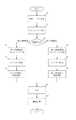
図6は、本実施形態の画像読取装置におけるイメージセンサのフローチャートである。 FIG. 6 is a flowchart of the image sensor in the image reading apparatus of the present embodiment.
ユーザーは、外部装置18のドライバのユーザインタフェース上で、読取範囲、読取解像度、画像処理等の読取条件の設定を行う(ステップS1)。 The user sets reading conditions such as a reading range, a reading resolution, and image processing on the user interface of the driver of the external device 18 (step S1).
ユーザーによりスキャンボタンが押下されると(ステップS2)、画像読取装置1のシステムコントローラ17は外部装置18から受信した読取条件の情報を受け取り、指定されている読取解像度に応じて第1又は第2の転送レジスタのどちらを使用するかを選択する(ステップS3)。 When the scan button is pressed by the user (step S2), the system controller 17 of the
第1の解像度が指定されている場合、第1の解像度に応じたクロックパルスがクロックパルス生成部21により生成され(ステップS4)、生成されたクロックパルスが第1の転送ゲート25及び第1の転送レジスタ26に供給され(ステップS5)、第1の解像度で画像の読取を行う(ステップS6)。When the first resolution is designated, a clock pulse corresponding to the first resolution is generated by the clock pulse generation unit21 (step S4), and the generated clock pulse is transmitted to the
また、第2の解像度が指定されている場合、第2の解像度に応じたクロックパルスがクロックパルス生成部21により生成され(ステップS7)、生成されたクロックパルスが第1の転送ゲート25、第2の転送ゲート27及び第1の転送レジスタ26、第2の転送レジスタ28に供給され(ステップS8)、第2の解像度で画像の読取を行う(ステップS9)。 When the second resolution is designated, a clock pulse corresponding to the second resolution is generated by the clock pulse generation unit 21 (step S7), and the generated clock pulse is transferred to the
イメージセンサから出力された読取画像信号にAFEや画像処理等を施して画像データを生成する(ステップS10,S11)。 Image data is generated by subjecting the read image signal output from the image sensor to AFE or image processing (steps S10 and S11).
(第2の実施形態)
図7は、本実施形態のクロックパルスCLK1及びCLK2の波形図である。第1の実施形態に対して、選択されなかった転送レジスタに不要な電荷が何らかの要因で貯まってしまった場合、転送用のクロックパルスの1/Nの低い周波数のクロックパルスを供給することで、不要な電荷を排除することができる。(Second Embodiment)
FIG. 7 is a waveform diagram of the clock pulses CLK1 and CLK2 of the present embodiment. In contrast to the first embodiment, when unnecessary charges are stored in the transfer registers that are not selected for some reason, by supplying a clock pulse having a low frequency of 1 / N of the transfer clock pulse, Unnecessary charges can be eliminated.
第1の解像度が指定されている場合、クロックパルスCLK1のシフトパルスSHがハイになったタイミングで第1の転送ゲート25が駆動され、受光素子アレイ24において光電変換された電荷が転送レジスタ26に移動する。そして、転送レジスタ26にクロックパルスCLK1の転送パルスΦ1とΦ2を同期させながら交互に供給することで、転送レジスタ26に移動した電荷を画素毎の電気信号として外部に出力する。 When the first resolution is designated, the
このとき、クロックパルスCLK2のシフトパルスSHがローであるため、第2の転送ゲート27は駆動されず、転送レジスタ28には受光素子24からの電荷は転送されない。また、クロックパルスCLK2の転送パルスΦ1及びΦ2が、クロックパルスCLK1の転送パルスΦ1及びΦ2よりも低い周波数で供給されており、第2の転送レジスタ28にある無駄な電荷を外部に排出することができる。 At this time, since the shift pulse SH of the clock pulse CLK2 is low, the
また、第2の解像度が指定されている場合、クロックパルスCLK1のシフトパルスSHがハイになったタイミングで第1の転送ゲート25が駆動され、受光素子アレイ24において光電変換された電荷が第1の転送レジスタ26に移動する。続いて、クロックパルスCLK2のシフトパルスSHがハイになったタイミングで第2の転送ゲート27が駆動され、第1の転送レジスタ26に移動した電荷がさらに第2の転送レジスタ28に移動する。そして、第2の転送レジスタ28にクロックパルスCLK2の転送パルスΦ1とΦ2を同期させながら交互に供給することで、第2の転送レジスタ28に移動した第1の転送レジスタ26のN画素分の電荷を加算して1画素の電気信号として外部に出力する。 When the second resolution is designated, the
このとき、クロックパルスCLK1の転送パルスΦ1とΦ2は、クロックパルスCLK1のシフトパルスSHがローであるときに、クロックパルスCLK2の転送パルスΦ1とΦ2よりも低い周波数で供給されており、第1の転送レジスタ26にある無駄な電荷を外部に排出することができる。 At this time, the transfer pulses Φ1 and Φ2 of the clock pulse CLK1 are supplied at a lower frequency than the transfer pulses Φ1 and Φ2 of the clock pulse CLK2 when the shift pulse SH of the clock pulse CLK1 is low. Wasteful charges in the
1 画像読取装置
2 原稿台ガラス
3 キャリッジ
4 ガイドシャフト
5 原稿カバー
6 モータ回路
7 原稿
8 光源
9 レンズ
10 イメージセンサ
11_1〜11_3 ミラー
12 AFE
13 シェーディング補正回路
14 画像処理回路
15 インターフェイス回路
16 光源用点灯回路
17 システムコントローラ
18 外部装置
19 解像度信号
20 イメージセンサの出力
21 クロックパルス生成部
22 第1の解像度用クロックパルス(CLK1)供給線
23 第2の解像度用クロックパルス(CLK2)供給線
24 受光素子アレイ
25 第1の転送ゲート
26 第1の転送レジスタ
27 第2の転送ゲート
28 第2の転送レジスタ
DESCRIPTION OF
DESCRIPTION OF
Claims (3)
Translated fromJapanese前記受光素子アレイにおいて光電変換された電荷信号を第1の解像度で外部に転送する第1の転送レジスタと、
前記受光素子アレイにおいて光電変換された電荷信号を前記第1の解像度の1/N(Nは自然数)である第2の解像度で外部に転送する第2の転送レジスタと、
前記第1の転送レジスタ又は前記第2の転送レジスタのどちらを用いて前記電荷信号を外部に転送するのかを選択する選択手段とを有し、
前記選択手段は、選択する転送レジスタに第1の周波数の転送クロックを供給し、選択しない転送レジスタに前記第1の周波数よりも低い第2の周波数のクロックを供給することを特徴とするリニアイメージセンサ。A light receiving element array in which a plurality of light receiving elements that photoelectrically convert incident light into electric charges are disposed;
A first transfer register for transferring a charge signal photoelectrically converted in the light receiving element array to the outside at a first resolution;
A second transfer register that transfers the charge signal photoelectrically converted in the light receiving element array to the outside at a second resolution that is 1 / N (N is a natural number) of the first resolution;
Have a selecting means for selecting whether to transfer the charge signals to the outside using either of the first transfer register and the second transferregister,
The selection unit supplies a transfer clock having a first frequency to a transfer register to be selected, and supplies aclock having a second frequency lower than the first frequency to a transfer register not to be selected. Sensor.
Priority Applications (1)
| Application Number | Priority Date | Filing Date | Title |
|---|---|---|---|
| JP2004218824AJP3944200B2 (en) | 2004-07-27 | 2004-07-27 | Linear image sensor and image reading apparatus |
Applications Claiming Priority (1)
| Application Number | Priority Date | Filing Date | Title |
|---|---|---|---|
| JP2004218824AJP3944200B2 (en) | 2004-07-27 | 2004-07-27 | Linear image sensor and image reading apparatus |
Publications (2)
| Publication Number | Publication Date |
|---|---|
| JP2006041918A JP2006041918A (en) | 2006-02-09 |
| JP3944200B2true JP3944200B2 (en) | 2007-07-11 |
Family
ID=35906433
Family Applications (1)
| Application Number | Title | Priority Date | Filing Date |
|---|---|---|---|
| JP2004218824AExpired - Fee RelatedJP3944200B2 (en) | 2004-07-27 | 2004-07-27 | Linear image sensor and image reading apparatus |
Country Status (1)
| Country | Link |
|---|---|
| JP (1) | JP3944200B2 (en) |
Families Citing this family (1)
| Publication number | Priority date | Publication date | Assignee | Title |
|---|---|---|---|---|
| JP4601630B2 (en)* | 2007-01-12 | 2010-12-22 | ルネサスエレクトロニクス株式会社 | Linear image sensor |
- 2004
- 2004-07-27JPJP2004218824Apatent/JP3944200B2/ennot_activeExpired - Fee Related
Also Published As
| Publication number | Publication date |
|---|---|
| JP2006041918A (en) | 2006-02-09 |
Similar Documents
| Publication | Publication Date | Title |
|---|---|---|
| US8693063B2 (en) | Image-reading device | |
| JP2007184907A (en) | Image reading apparatus and image reading method | |
| JP3165731B2 (en) | Image reading device | |
| JP3780983B2 (en) | Image reading device | |
| JP2007013743A (en) | Image reading device | |
| JP3706817B2 (en) | Image processing apparatus and processing method thereof | |
| JP3944200B2 (en) | Linear image sensor and image reading apparatus | |
| US6818878B2 (en) | Multi-resolution charge-coupled device sensing device | |
| USRE40628E1 (en) | Apparatus for reducing exposing time of an image processing system | |
| US6639202B2 (en) | Multi-resolution charge-coupled device (CCD) sensing apparatus | |
| JP3631597B2 (en) | Image reading device | |
| JP2003219172A (en) | Image processing apparatus and image forming apparatus | |
| JPS60157A (en) | image input device | |
| JP2005269340A (en) | Photoelectric conversion device and reading device | |
| JP2004289289A (en) | Image reading device and image forming device | |
| JP4904317B2 (en) | Image reading apparatus, and image storage apparatus and image forming apparatus including the same | |
| JP4658677B2 (en) | Image reading device | |
| JPH11308409A (en) | Image reading apparatus and image reduction reading method thereof | |
| JPH02121471A (en) | Image reading device | |
| JP2000151899A (en) | Image reading device and integrated circuit device for image reading control | |
| JPH03241968A (en) | Picture reader | |
| JP2004201130A (en) | Image input device and image input program | |
| JPH02177665A (en) | Method and device for reading picture | |
| JPS59223061A (en) | Image reading device | |
| JPS63240259A (en) | image reading device |
Legal Events
| Date | Code | Title | Description |
|---|---|---|---|
| A977 | Report on retrieval | Free format text:JAPANESE INTERMEDIATE CODE: A971007 Effective date:20060623 | |
| A131 | Notification of reasons for refusal | Free format text:JAPANESE INTERMEDIATE CODE: A131 Effective date:20060718 | |
| A521 | Written amendment | Free format text:JAPANESE INTERMEDIATE CODE: A523 Effective date:20060915 | |
| TRDD | Decision of grant or rejection written | ||
| A01 | Written decision to grant a patent or to grant a registration (utility model) | Free format text:JAPANESE INTERMEDIATE CODE: A01 Effective date:20070320 | |
| A61 | First payment of annual fees (during grant procedure) | Free format text:JAPANESE INTERMEDIATE CODE: A61 Effective date:20070406 | |
| R150 | Certificate of patent or registration of utility model | Free format text:JAPANESE INTERMEDIATE CODE: R150 | |
| FPAY | Renewal fee payment (event date is renewal date of database) | Free format text:PAYMENT UNTIL: 20110413 Year of fee payment:4 | |
| FPAY | Renewal fee payment (event date is renewal date of database) | Free format text:PAYMENT UNTIL: 20130413 Year of fee payment:6 | |
| FPAY | Renewal fee payment (event date is renewal date of database) | Free format text:PAYMENT UNTIL: 20130413 Year of fee payment:6 | |
| FPAY | Renewal fee payment (event date is renewal date of database) | Free format text:PAYMENT UNTIL: 20140413 Year of fee payment:7 | |
| LAPS | Cancellation because of no payment of annual fees |