JP3943437B2 - Liquid crystal display - Google Patents
Liquid crystal displayDownload PDFInfo
- Publication number
- JP3943437B2 JP3943437B2JP2002135746AJP2002135746AJP3943437B2JP 3943437 B2JP3943437 B2JP 3943437B2JP 2002135746 AJP2002135746 AJP 2002135746AJP 2002135746 AJP2002135746 AJP 2002135746AJP 3943437 B2JP3943437 B2JP 3943437B2
- Authority
- JP
- Japan
- Prior art keywords
- liquid crystal
- crystal display
- frame member
- display device
- display unit
- Prior art date
- Legal status (The legal status is an assumption and is not a legal conclusion. Google has not performed a legal analysis and makes no representation as to the accuracy of the status listed.)
- Expired - Fee Related
Links
- 239000004973liquid crystal related substanceSubstances0.000titleclaimsdescription116
- 239000000758substrateSubstances0.000claimsdescription39
- 230000006835compressionEffects0.000claimsdescription18
- 238000007906compressionMethods0.000claimsdescription18
- 239000006260foamSubstances0.000claimsdescription10
- 229920000642polymerPolymers0.000claimsdescription7
- 239000000203mixtureSubstances0.000claimsdescription6
- 230000002093peripheral effectEffects0.000claimsdescription2
- 239000011521glassSubstances0.000description15
- 239000004814polyurethaneSubstances0.000description8
- 238000005286illuminationMethods0.000description7
- 229920002635polyurethanePolymers0.000description6
- -1for exampleSubstances0.000description5
- 230000035939shockEffects0.000description5
- 239000004698PolyethyleneSubstances0.000description4
- 230000000052comparative effectEffects0.000description4
- 229920000573polyethylenePolymers0.000description4
- 239000002390adhesive tapeSubstances0.000description2
- 230000000694effectsEffects0.000description2
- 239000000463materialSubstances0.000description2
- 229920003023plasticPolymers0.000description2
- 239000004033plasticSubstances0.000description2
- 238000007789sealingMethods0.000description2
- 241000282320Panthera leoSpecies0.000description1
- 239000004793PolystyreneSubstances0.000description1
- 229920005830Polyurethane FoamPolymers0.000description1
- 239000000853adhesiveSubstances0.000description1
- 230000001070adhesive effectEffects0.000description1
- 230000003139buffering effectEffects0.000description1
- 210000000078clawAnatomy0.000description1
- 238000010586diagramMethods0.000description1
- 239000013013elastic materialSubstances0.000description1
- 229920001971elastomerPolymers0.000description1
- 230000006355external stressEffects0.000description1
- 238000005259measurementMethods0.000description1
- 239000002184metalSubstances0.000description1
- 238000000034methodMethods0.000description1
- 229920002223polystyrenePolymers0.000description1
- 239000011496polyurethane foamSubstances0.000description1
- 239000004800polyvinyl chlorideSubstances0.000description1
- 229920000915polyvinyl chloridePolymers0.000description1
- 239000011347resinSubstances0.000description1
- 229920005989resinPolymers0.000description1
- 230000035882stressEffects0.000description1
Images


Classifications
- G—PHYSICS
- G02—OPTICS
- G02F—OPTICAL DEVICES OR ARRANGEMENTS FOR THE CONTROL OF LIGHT BY MODIFICATION OF THE OPTICAL PROPERTIES OF THE MEDIA OF THE ELEMENTS INVOLVED THEREIN; NON-LINEAR OPTICS; FREQUENCY-CHANGING OF LIGHT; OPTICAL LOGIC ELEMENTS; OPTICAL ANALOGUE/DIGITAL CONVERTERS
- G02F1/00—Devices or arrangements for the control of the intensity, colour, phase, polarisation or direction of light arriving from an independent light source, e.g. switching, gating or modulating; Non-linear optics
- G02F1/01—Devices or arrangements for the control of the intensity, colour, phase, polarisation or direction of light arriving from an independent light source, e.g. switching, gating or modulating; Non-linear optics for the control of the intensity, phase, polarisation or colour
- G02F1/13—Devices or arrangements for the control of the intensity, colour, phase, polarisation or direction of light arriving from an independent light source, e.g. switching, gating or modulating; Non-linear optics for the control of the intensity, phase, polarisation or colour based on liquid crystals, e.g. single liquid crystal display cells
- G02F1/133—Constructional arrangements; Operation of liquid crystal cells; Circuit arrangements
- G02F1/1333—Constructional arrangements; Manufacturing methods
- G02F1/133308—Support structures for LCD panels, e.g. frames or bezels
- G—PHYSICS
- G02—OPTICS
- G02F—OPTICAL DEVICES OR ARRANGEMENTS FOR THE CONTROL OF LIGHT BY MODIFICATION OF THE OPTICAL PROPERTIES OF THE MEDIA OF THE ELEMENTS INVOLVED THEREIN; NON-LINEAR OPTICS; FREQUENCY-CHANGING OF LIGHT; OPTICAL LOGIC ELEMENTS; OPTICAL ANALOGUE/DIGITAL CONVERTERS
- G02F2201/00—Constructional arrangements not provided for in groups G02F1/00 - G02F7/00
- G02F2201/50—Protective arrangements
- G02F2201/503—Arrangements improving the resistance to shock
Landscapes
- Physics & Mathematics (AREA)
- Nonlinear Science (AREA)
- Liquid Crystal (AREA)
- Mathematical Physics (AREA)
- Chemical & Material Sciences (AREA)
- Crystallography & Structural Chemistry (AREA)
- General Physics & Mathematics (AREA)
- Optics & Photonics (AREA)
- Devices For Indicating Variable Information By Combining Individual Elements (AREA)
Description
Translated fromJapanese【0001】
【発明の属する技術分野】
本発明は、耐衝撃性が優れた液晶表示装置に関する。
【0002】
【従来の技術】
一般に液晶表示装置は、液晶表示ユニットと、この液晶表示ユニットに駆動信号を入力するための駆動回路と、これらを一体に保持する枠部材とを有している。液晶表示ユニットは基本的に、2枚のガラス基板間に液晶組成物を封入してなる液晶パネル、前記ガラス基板の外側面に貼着された偏光板、位相差板などから構成されている。これに加えて、液晶表示ユニットが透過型あるいは半透過型の場合は液晶パネルの裏面(非表示面)にバックライト装置が装着されたり、また液晶表示ユニットが反射型の場合は液晶パネルの表面(画像表示面)にフロントライト装置、液晶表示ユニット内に反射板が装着されることもある。このような構成の液晶表示ユニットが携帯電話機やPDA(personal digital assistant、携帯情報端末)などの小型機器に用いられるようになると、機器全体の薄型化・軽量化のために、前記の液晶パネルに用いられているガラス基板や枠部材にも極度の薄型化・軽量化が求められるようになってきた。例えば前記ガラス基板の板厚は、従来1.1mm厚〜0.7mm厚程度であったものが、0.55mm厚〜0.5mm厚、あるいは場合によって0.4mm厚程度まで薄型化されてきている。
【0003】
【発明が解決しようとする課題】
前記のように部材が極度に薄型化・軽量化されると、機器の取り扱い、携帯時の機械的なねじれ、衝撃などによって液晶パネルや枠部材が破損しやすくなるという問題が発生している。特に携帯電話機やPDAなどのモバイル機器では、携帯時に誤って路面や床に落としたり、また機器の上に重量物を落とすというような事故も考えられる。そこで、薄型・軽量なモバイル機器に用いられる液晶表示装置では、よりいっそうの耐衝撃性が求められるようになってきた。また、他の問題として、落下時などの衝撃によって液晶パネル内に気泡が発生するという問題も生じている。これは液晶組成物中に溶解していたガス成分、例えば空気が衝撃による急激な圧力変動によって気化することによって起こる現象と考えられている。
【0004】
薄型液晶表示装置の耐衝撃性を改善するために従来から、例えば、液晶パネルと、駆動回路を搭載した回路基板と、導電性ゴムを含む弾性材を介してこの両者を所定の相対位置に固定する金属フレームとを有する液晶表示装置、あるいは液晶パネルと、駆動回路を実装したフレキシブル基板と、両者を覆うように配置されたフレームとからなり、フレキシブル基板が液晶パネルの電極端子配列面と一平面をなし、この接続部とフレームとの間に緩衝材を設けた液晶表示装置などが提案されている。しかしこれらは何れも、液晶パネルの電極端子とフレキシブル基板の電極端子との接続部を衝撃から保護しようとするものであり、これによって液晶パネル自体も保護されるとはいえ、極度に薄型化された液晶パネルの破損や気泡の発生などには効果が期待できなかった。本発明は前記の課題を解決するためになされたものであって、従ってその目的は、薄型化・軽量化した場合にも耐衝撃性が優れた液晶表示装置を提供することにある。
【0005】
【課題を解決するための手段】
前記の課題を解決するために本発明は、2枚の基板間に液晶組成物を封入した液晶パネルを含む液晶表示ユニットが一方の面を画像表示面として他方の面を非表示面として枠部材に収容されてなり、前記枠部材が、前記液晶表示ユニットの非表示面に対向する底板を有し、この底板の一部に開口部が形成され、前記液晶表示ユニットの前記非表示面に、前記底板の開口部に挿入される緩衝部材が装着されてなる液晶表示装置を提供する。
【0006】
一般に液晶パネルの衝撃による破損や気泡の発生は、外部から伝達される衝撃に起因する。本発明の前記液晶表示装置においては、液晶表示ユニットの非表示面側に緩衝部材が装着されているので、この緩衝部材が液晶パネルの非表示面側に伝達された衝撃波を吸収し、破損や気泡の発生を有効に防止することができる。この場合、厚い緩衝部材が非表示面側に単に装着されていると緩衝部材の厚み分だけ液晶表示装置全体の厚みが増大することになり、薄型化の要求に応えられない。本発明において緩衝部材は枠部材の底板に形成された開口部に挿入されているので、緩衝部材の装着によって液晶表示装置全体の厚みが増大することはない。
【0007】
前記の緩衝部材は板状の高分子発泡体からなり、かつこの緩衝部材の厚みは枠部材の底板の厚みと等しいか又はそれ以下であることが好ましい。 更に、緩衝部材が高分子発泡体である場合、発泡体に含まれる気泡の平均径は15μm〜60μmの範囲内であることが好ましい。また前記の緩衝部材は、圧縮荷重(圧縮速度1.0mm/min、圧縮率25%時)が0.6kg/cm2〜0.02kg/cm2の範囲内であり、かつ圧縮永久ひずみ(JIS-K6401準拠)が0.5%〜5.0%の範囲内であることが好ましい。
【0008】
液晶パネルに破損や気泡の発生をもたらす衝撃を有効に吸収し得る緩衝部材の特性を探索した結果、圧縮荷重特性と圧縮永久ひずみ特性とが重要であり、特にこれらの特性が上記の数値範囲内のとき、有効な緩衝効果が得られることがわかった。この特性を満足する素材としては高分子発泡体が挙げられる。本発明に好適に用いられる高分子発泡体の例としては、例えばポリスチレン、ポリウレタン、ポリエチレン、又は軟質ポリ塩化ビニルなどの発泡体を挙げることができる。特にポリエチレン及びポリウレタンの発泡体は、圧縮永久ひずみが低く、好適な数値範囲内にあって効果が高い。この高分子発泡体が板状又はシート状に成形され、その厚みが枠部材の底板の厚みと等しいか又はそれ以下とされていれば、液晶表示ユニットが枠部材に収容された状態で緩衝部材が枠部材の底板より外側に突出せず、外部応力から保護される。
【0009】
本発明はまた、前記液晶パネルの辺部にフレキシブル基板が接続され、このフレキシブル基板が前記枠部材の外側面に沿って湾曲し、前記底板の開口部に被せられ、前記フレキシブル基板において前記開口部に面する位置に回路部品が搭載されてなる液晶表示装置を提供する。このとき、ICチップなどの回路部品がフレキシブル基板上の前記開口部を覆う位置の外側面に配置されていることが好ましい。
【0010】
フレキシブル基板が枠部材の外側に沿って回り込み、底板の開口部を覆っていて、ICチップなどの回路部品がフレキシブル基板上の前記開口部外側に配置されていると、液晶表示装置が落下した際に回路部材が液晶パネルの裏面側に衝突しようとしても緩衝部材が衝撃を緩和する。
【0011】
本発明は更に、前記液晶表示ユニットの画像表示面と前記枠部材の上面とが略面一とされ、その境界が衝撃吸収シートで覆われてなる液晶表示装置を提供する。
落下などによって液晶表示装置の側部が衝撃を受けると、衝撃応力の一部は枠部材の縁部から、この縁部と接触する液晶表示ユニットの辺部に伝達され、液晶パネルなどの破損をもたらす場合がある。液晶表示ユニットの画像表示面と前記枠部材の上面とが面一とされ、その境界が衝撃吸収シートで覆われていれば、この衝撃吸収シートによって衝撃波が吸収されるので、液晶表示ユニットは側部からの衝撃に対しても保護されることになる。
【0012】
【発明の実施の形態】
次に本発明の実施の形態を具体例によって説明するがこれらは本発明を何ら制限するものではない。また、添付の図面は本発明の思想を説明するためのものであって、説明に不用な要素は省略しまた各要素の形状や寸法比は必ずしも実際のものを反映していない。
【0013】
(実施形態1)
図1は本実施形態の液晶表示装置の構成を示す断面図である。図2は前記液晶表示装置の構成要素を分離して示す斜視図である。
本実施形態は反射型の液晶表示装置であり、概略、液晶表示ユニット1と、枠部材2と、フレキシブル基板3とから構成されている。このうち液晶表示ユニット1は、第1のガラス基板11と第2のガラス基板12との間にシール部材13に囲まれて液晶組成物14が封入されてなる液晶パネル15と、この液晶パネル15の一面側の画像表示面S側に貼着された偏光板及び2枚の位相差板からなる光制御板16とからなっている。第1ガラス基板11の一辺部はシール部材13の外側に延びて電極端子部17を形成している。電極端子部17を除く液晶パネル15の寸法は例えば40mm×50mmであり、第1及び第2のガラス基板11,12の板厚は例えば0.55tである。なお、第1ガラス基板11及び第2ガラス基板12の双方又は一方の内側面には液晶駆動電極、カラーフィルタ、反射板、配向膜などが設けられているがここでは図示及び説明を省略する。
【0014】
第2ガラス基板12の裏面側(他面側)、すなわち液晶表示ユニット1の非表示面B側中央部には緩衝部材18が貼着されている。この緩衝部材18は、例えば厚み0.3mmの発泡ポリウレタンのシートを例えば19mm×7.5mmの長方形に裁断して作成したものであり、両面テープで非表示面B側の中央部に貼り付けられている。この発泡ポリウレタンからなる緩衝部材18は、圧縮荷重(圧縮速度1.0mm/min、圧縮率25%時)が0.2kg/cm2であり、圧縮永久ひずみ(JIS-K6401準拠)が2.0%であった。
【0015】
枠部材2は、周壁を構成する枠部21と底板22とが一体に成形されたプラスチックのモールド部材であって、概略長方形の受け皿状をなし、底板22の厚みは例えば0.3mmである。底板22の中央付近には例えば20mm×8mmの矩形状の開口部23が形成されている。液晶表示ユニット1は、画像表示面Sを表出させて、枠部21に囲まれた底板22の上に載置される。このとき液晶表示ユニット1に貼着された緩衝部材17は、底板22の開口部23に緩やかに嵌入される。また、底板22の外側面には、フレキシブル基板3を枠部材2に係止するための爪型の突起部25…が形成されている。
【0016】
フレキシブル基板3は、概略長方形の可撓性樹脂基盤からなり、一方の端部に液晶パネル接続用の端子部31が形成され、この端子部31が液晶表示ユニット1の第1ガラス基板11に形成された電極端子部17とACF(異方性導電フィルム)により接続されている。このフレキシブル基板3は、枠部材2の外側に引き出されて枠部材2の裏面側に回り込むように配置され、底板22の外面に沿って、開口部23を覆うように延在されている。フレキシブル基板3は好適な位置に設けられた突起部25によって底板22の外側面に係止されている。フレキシブル基板3の外面上で、開口部23を覆う領域R内には、ICチップなど厚みのある駆動用の回路部品32…が複数実装されている。これらの回路部品32…及び電極端子部17は、フレキシブル基板3に形成された図示しないプリント配線によって互いに接続されている。またこのプリント配線は図示しない端子部を介して外部の回路に接続されるようになっている。
【0017】
(実施形態2)
図3は第2実施形態の液晶表示装置の構成を示す断面図である。
本実施形態は反射型の液晶表示装置であり、概略、液晶表示ユニット1と、フロントライト装置4と、枠部材2と、フレキシブル基板3とから構成されている。このうち液晶表示ユニット1及びフレキシブル基板3は実施形態1で説明したものと実質的に同様であるので詳しい説明は省略し、第1実施形態の構成と同一の部分には同一の符号を付した。
【0018】
フロントライト装置4は、透明な板状体でその一方の面にプリズム状の凹凸が配列されてなる照明板41と図示しない光源部とからなり、光源部からの光を照明板41の側面から入射し、照明板41の内面反射により液晶表示ユニット1に向けて照明光を面状に照射する装置であり、液晶表示ユニット1内の図示しない反射板で反射された前記の照明光は光制御板16と照明板41とを順次透過して観察者が画像を視認できるようになっている。本実施形態においてフロントライト装置4の照明板41は、両面接着テープ43により液晶表示ユニット1の光制御板16の上に貼着されている。従って本実施形態においては照明板41の外向き面が画像表示面Sになっている。また照明板41の各辺部には段差状の切欠42が形成されている。
【0019】
枠部材2は、枠部21と底板22とが一体に成形されたプラスチックのモールド部材であって、実施形態1で説明したものと実質的に同様であるが、ただし枠部21の上辺が内側に延び、額縁部26を形成している。この額縁部26は、液晶表示ユニット1とフロントライト装置4とが枠部材2内に収容された状態で照明板41の切欠42と係合しフロントライト装置4及び液晶表示ユニット1の抜け落ちを防止すると共に、その上面は照明板41の画像表示面Sと面一となるように調整されている。そしてこの額縁部26と照明板41との境界には、粘着剤によって、発泡ポリウレタンからなる衝撃吸収シート44が貼着されている。
【0020】
【実施例】
(耐衝撃性試験)
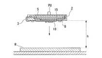
実施形態1の液晶表示装置を実施例1として耐衝撃性を以下の方法で試験した。図4は耐衝撃性試験の実施状態を示す概略図である。パネル寸法は約40×50mm(板厚0.55tのガラス基板利用)の液晶パネルに偏光板と位相差板を2枚貼付し、液晶パネルの端部に駆動用ICチップを複数搭載した構成であり、液晶パネルの周囲に厚さ0.3mmの樹脂モールドの枠状構造体を嵌め込んだ。このモールドには約20×8mmの開口部が形成されている。この開口部に対して液晶パネルの背面側に発泡性ポリウレタン(圧縮残留歪2.0%(JISK6401)、圧縮荷重0.2kg/cm2)からなる板厚0.3mm、寸法19×7.5mmの緩衝部材18を両面テープで貼り付けた。
図4に示すように、本液晶表示装置の画像表示面Sの中央部に荷重計測用のピックアップセンサ(リオン社製モデルPV90B)PUを両面テープ(厚み25μm)で貼着した。この供試体を、非表示面Bの側を下にして、机上のラワン板(板厚30mm)上方に水平な状態で保持し、落下高さhを10cmから100cmまで変化させ自然落下させた。
【0021】
各落下試験ごとに供試体の破損状況を観察し、破損発生高さと破損部位とを記録した。同様に各落下試験ごとに供試体の液晶パネル内の気泡発生状況を観察し、気泡発生状況を記録した。また、破損・気泡発生の有無に係わらず、落下させたときピックアップセンサPUにより計測された荷重(G)を測定し、測定結果を図5に示した。
【0022】
(比較例1)
比較のため、実施形態1と同様の構成で、ただし枠部材の底板に開口部を形成せず、かつ液晶表示ユニットの非表示面Bに緩衝部材を貼着しない比較例の液晶表示装置を作成し、実施形態1のものと同様に上記の耐衝撃性試験を行った。その結果を図5に示す。
【0023】
図5に示す耐衝撃性試験の結果、実施形態1の液晶表示装置は緩衝部材を持たない比較例1に比べ、破損発生高さが大幅に向上し、衝撃も減少したことがわかる。実施例1の液晶表示装置では落下高さ100cmまで液晶表示装置に破損が生じることがなく、液晶パネル内に衝撃による気泡も生じなかった。更に落下高さを130cmとしたところ液晶表示装置が破損した。
【0024】
(実施例2)
実施形態1と同様の構成で、ただし緩衝部材18の厚みを0.5mmとして実施形態1の場合と同様の耐衝撃性試験を行った。用いた緩衝部材はポリウレタン製で、圧縮荷重(圧縮速度1.0mm/min、圧縮率25%時)は0.2kg/cm2であり、圧縮永久ひずみ(JIS-K6401準拠)は2.5%であった。
この実施例2の試験では落下高さ150cmまで液晶表示装置の破損は生じなかった。
【0025】
(実施例3)
実施例1と同様の構成で、ただし緩衝部材18として厚み0.3mmの発泡ポリエチレンシートを19mm×7.5mmの寸法に裁断したものを用いた。この発泡ポリエチレンシートは圧縮荷重が0.40kg/cm2であり、圧縮永久ひずみ(JIS-K6401準拠)が4.5%であった。この試験体について実施例1の場合と同様の耐衝撃性試験を行ったところ、落下高さ90cmまで液晶表示装置の破損は発生しなかった。
以上の試験結果から、いずれの実施例1、2、3においても比較例よりも優れた衝撃吸収性能が実証された。
【0026】
【発明の効果】
本発明の液晶表示装置は、枠部材の底板に開口部が形成され、液晶表示ユニットの非表示面側に、前記開口部に挿入し得る緩衝部材が装着されているので、液晶表示装置が大幅に薄型化・軽量化された場合にも、耐衝撃性が優れた特性を得ることができる。
本発明において緩衝部材が板状の高分子発泡体からなり、かつこの緩衝部材の厚みが前記枠部材の底板の厚みと等しいか又はそれ以下であるならば液晶表示装置全体の厚みを増加することなく耐衝撃性に優れたものが得られる。
【0027】
本発明は更に、液晶表示ユニットの画像表示面と枠部材の上面とが略面一とされ、境界が衝撃吸収シートで覆われてなるので、落下などによって液晶表示装置の側部が衝撃を受けると、衝撃吸収シートによって衝撃が吸収されるので、液晶表示ユニットは側部からの衝撃に対しても保護され、衝撃に強い構造とされる。
【図面の簡単な説明】
【図1】 図1は本発明に係る実施形態1の液晶表示装置の構成を示す断面図である。
【図2】 図2は前記液晶表示装置の構成要素を分離して示す斜視図である。
【図3】 図3は本発明に係る実施形態2の液晶表示装置の構成を示す断面図である。
【図4】 図4は耐衝撃性試験の実施状態を示す概略図である。
【図5】 図5は液晶表示装置の落下試験結果を示す図である。
【符号の説明】
1…液晶表示ユニット、2…枠部材、3…フレキシブル基板、4…フロントライト装置、11…第1ガラス基板、12…第2ガラス基板、13…シール部材、14…液晶組成物、15…液晶パネル、16…光制御板、17…電極端子部、18…緩衝部材、21…枠部、22…底板、23…開口部、25…爪部、26…額縁部、31…端子部、32…回路部材、41…照明板、42…切欠、43…両面接着テープ、44…衝撃吸収シート。[0001]
BACKGROUND OF THE INVENTION
The present invention relates to a liquid crystal display device having excellent impact resistance.
[0002]
[Prior art]
In general, a liquid crystal display device includes a liquid crystal display unit, a drive circuit for inputting a drive signal to the liquid crystal display unit, and a frame member that integrally holds these. The liquid crystal display unit basically includes a liquid crystal panel in which a liquid crystal composition is sealed between two glass substrates, a polarizing plate attached to an outer surface of the glass substrate, a retardation plate, and the like. In addition, when the liquid crystal display unit is a transmissive or transflective type, a backlight device is mounted on the back surface (non-display surface) of the liquid crystal panel, or when the liquid crystal display unit is a reflective type, the surface of the liquid crystal panel A front light device may be mounted on the (image display surface), and a reflector may be mounted in the liquid crystal display unit. When the liquid crystal display unit having such a configuration is used in small devices such as mobile phones and PDAs (personal digital assistants, personal digital assistants), the above-mentioned liquid crystal panel is used to reduce the overall thickness and weight of the device. The glass substrates and frame members used have been required to be extremely thin and light. For example, the thickness of the glass substrate is conventionally about 1.1 mm to 0.7 mm, but has been thinned to about 0.55 to 0.5 mm, or in some cases about 0.4 mm. Yes.
[0003]
[Problems to be solved by the invention]
As described above, when the member is extremely thin and light, there is a problem that the liquid crystal panel and the frame member are easily damaged due to handling of the device, mechanical twisting at the time of carrying, impact, and the like. Especially in mobile devices such as mobile phones and PDAs, accidents such as accidentally dropping on the road surface or floor when carrying, or dropping heavy objects on the device may be considered. Therefore, liquid crystal display devices used for thin and light mobile devices have been required to have higher impact resistance. As another problem, there is a problem that bubbles are generated in the liquid crystal panel due to an impact such as dropping. This is considered to be a phenomenon that occurs when a gas component dissolved in the liquid crystal composition, for example, air, is vaporized by a sudden pressure fluctuation due to an impact.
[0004]
Conventionally, in order to improve the impact resistance of a thin liquid crystal display device, for example, a liquid crystal panel, a circuit board on which a drive circuit is mounted, and an elastic material containing conductive rubber are fixed to a predetermined relative position. A liquid crystal display device having a metal frame or a liquid crystal panel, a flexible substrate on which a drive circuit is mounted, and a frame arranged so as to cover both, and the flexible substrate is flush with the electrode terminal arrangement surface of the liquid crystal panel There has been proposed a liquid crystal display device in which a buffer material is provided between the connecting portion and the frame. However, both of these are intended to protect the connection portion between the electrode terminal of the liquid crystal panel and the electrode terminal of the flexible substrate from an impact, and although this protects the liquid crystal panel itself, it is extremely thinned. We could not expect any effect on the damage of the liquid crystal panel and the generation of bubbles. SUMMARY OF THE INVENTION The present invention has been made to solve the above-described problems. Accordingly, it is an object of the present invention to provide a liquid crystal display device having excellent impact resistance even when it is thin and light.
[0005]
[Means for Solving the Problems]
In order to solve the above-mentioned problems, the present invention provides a liquid crystal display unit including a liquid crystal panel in which a liquid crystal composition is sealed between two substrates, a frame member having one surface as an image display surface and the other surface as a non-display surface. The frame member has a bottom plate facing the non-display surface of the liquid crystal display unit, an opening is formed in a part of the bottom plate, and the non-display surface of the liquid crystal display unit Provided is a liquid crystal display device in which a buffer member inserted into the opening of the bottom plate is mounted.
[0006]
In general, breakage or bubble generation due to impact of a liquid crystal panel is caused by impact transmitted from the outside. In the liquid crystal display device of the present invention, since the buffer member is mounted on the non-display surface side of the liquid crystal display unit, the buffer member absorbs the shock wave transmitted to the non-display surface side of the liquid crystal panel, Generation of bubbles can be effectively prevented. In this case, if the thick buffer member is simply mounted on the non-display surface side, the thickness of the entire liquid crystal display device is increased by the thickness of the buffer member, and the demand for thinning cannot be met. In the present invention, since the buffer member is inserted into the opening formed in the bottom plate of the frame member, the thickness of the entire liquid crystal display device is not increased by the mounting of the buffer member.
[0007]
The buffer member is preferably made of a plate-like polymer foam, and the thickness of the buffer member is preferably equal to or less than the thickness of the bottom plate of the frame member. Furthermore, when the buffer member is a polymer foam, the average diameter of the bubbles contained in the foam is preferably in the range of 15 μm to 60 μm. The said buffer member, a compressive load (compression speed 1.0 mm / min,
[0008]
As a result of searching for the characteristics of the buffer member that can effectively absorb the impact that causes breakage and bubble generation on the liquid crystal panel, the compression load characteristics and the compression set characteristics are important. Especially, these characteristics are within the above numerical range. It was found that an effective buffering effect can be obtained. An example of a material that satisfies this characteristic is a polymer foam. Examples of the polymer foam suitably used in the present invention include foams such as polystyrene, polyurethane, polyethylene, or soft polyvinyl chloride. In particular, foams of polyethylene and polyurethane have a low compression set and are effective within a suitable numerical range. If the polymer foam is formed into a plate shape or a sheet shape, and the thickness is equal to or less than the thickness of the bottom plate of the frame member, the buffer member is accommodated in the state in which the liquid crystal display unit is accommodated in the frame member. Does not protrude outward from the bottom plate of the frame member, and is protected from external stress.
[0009]
According to the present invention, a flexible substrate is connected to a side portion of the liquid crystal panel, the flexible substrate is curved along the outer surface of the frame member, and is covered with the opening of the bottom plate. Provided is a liquid crystal display device in which circuit parts are mounted at a position facing the surface. At this time, it is preferable that a circuit component such as an IC chip is disposed on the outer surface of the position covering the opening on the flexible substrate.
[0010]
When the flexible substrate wraps around the outside of the frame member, covers the opening of the bottom plate, and a circuit component such as an IC chip is arranged outside the opening on the flexible substrate, the liquid crystal display device falls Even if the circuit member tries to collide with the back side of the liquid crystal panel, the buffer member alleviates the impact.
[0011]
The present invention further provides a liquid crystal display device in which the image display surface of the liquid crystal display unit and the upper surface of the frame member are substantially flush with each other and the boundary is covered with an impact absorbing sheet.
When the side of the liquid crystal display device receives an impact due to dropping or the like, part of the impact stress is transmitted from the edge of the frame member to the side of the liquid crystal display unit in contact with this edge, causing damage to the liquid crystal panel, etc. May bring. If the image display surface of the liquid crystal display unit and the upper surface of the frame member are flush with each other and the boundary is covered with the shock absorbing sheet, the shock absorbing sheet absorbs the shock wave. It will be protected against the impact from the part.
[0012]
DETAILED DESCRIPTION OF THE INVENTION
Next, embodiments of the present invention will be described by way of specific examples, but these do not limit the present invention. Further, the accompanying drawings are for explaining the idea of the present invention, elements not necessary for the explanation are omitted, and the shapes and dimensional ratios of the elements do not necessarily reflect actual ones.
[0013]
(Embodiment 1)
FIG. 1 is a cross-sectional view showing the configuration of the liquid crystal display device of this embodiment. FIG. 2 is a perspective view showing components of the liquid crystal display device separately.
The present embodiment is a reflective liquid crystal display device, and is roughly composed of a liquid crystal display unit 1, a
[0014]
A
[0015]
The
[0016]
The
[0017]
(Embodiment 2)
FIG. 3 is a cross-sectional view showing the configuration of the liquid crystal display device of the second embodiment.
The present embodiment is a reflective liquid crystal display device, and generally includes a liquid crystal display unit 1, a front light device 4, a
[0018]
The front light device 4 includes a
[0019]
The
[0020]
【Example】
(Impact resistance test)
The liquid crystal display device of Embodiment 1 was tested as Example 1 for impact resistance by the following method. FIG. 4 is a schematic view showing an implementation state of the impact resistance test. The panel dimensions are about 40x50mm (using a glass substrate with a thickness of 0.55t). Two polarizing plates and two phase plates are attached to the liquid crystal panel, and multiple drive IC chips are mounted on the edge of the liquid crystal panel. Yes, a resin-molded frame-like structure having a thickness of 0.3 mm was fitted around the liquid crystal panel. This mold has an opening of about 20 × 8 mm. The thickness of the foamed polyurethane (compressive residual strain 2.0% (JISK6401), compressive load 0.2 kg / cm2 ) 0.3 mm, dimension 19 x 7.5 mm The
As shown in FIG. 4, a load sensor pickup sensor (Lion model PV90B) PU was attached to the center of the image display surface S of the present liquid crystal display device with a double-sided tape (
[0021]
For each drop test, the state of breakage of the specimen was observed, and the occurrence height of the breakage and the breakage site were recorded. Similarly, the bubble generation state in the liquid crystal panel of the specimen was observed for each drop test, and the bubble generation state was recorded. Further, the load (G) measured by the pickup sensor PU when it was dropped was measured regardless of whether breakage or bubbles were generated, and the measurement result is shown in FIG.
[0022]
(Comparative Example 1)
For comparison, a liquid crystal display device of a comparative example having the same configuration as that of the first embodiment, except that no opening is formed in the bottom plate of the frame member and no buffer member is attached to the non-display surface B of the liquid crystal display unit is produced. Then, the impact resistance test was performed in the same manner as in the first embodiment. The result is shown in FIG.
[0023]
As a result of the impact resistance test shown in FIG. 5, it can be seen that the liquid crystal display device of Embodiment 1 has a significantly improved breakage height and reduced impact compared to Comparative Example 1 having no buffer member. In the liquid crystal display device of Example 1, the liquid crystal display device was not damaged up to a drop height of 100 cm, and no bubbles were generated in the liquid crystal panel due to impact. Furthermore, when the drop height was set to 130 cm, the liquid crystal display device was damaged.
[0024]
(Example 2)
The same impact resistance test as in the first embodiment was performed with the same configuration as in the first embodiment except that the thickness of the
In the test of Example 2, the liquid crystal display device was not damaged up to a drop height of 150 cm.
[0025]
Example 3
A configuration similar to that of Example 1 except that a foamed polyethylene sheet having a thickness of 0.3 mm was cut into a size of 19 mm × 7.5 mm as the
From the above test results, shock absorbing performance superior to that of the comparative example was demonstrated in any of Examples 1, 2, and 3.
[0026]
【The invention's effect】
In the liquid crystal display device of the present invention, the opening is formed in the bottom plate of the frame member, and the buffer member that can be inserted into the opening is mounted on the non-display surface side of the liquid crystal display unit. Even when it is made thinner and lighter, it is possible to obtain characteristics with excellent impact resistance.
In the present invention, if the buffer member is made of a plate-like polymer foam and the thickness of the buffer member is equal to or less than the thickness of the bottom plate of the frame member, the total thickness of the liquid crystal display device is increased. And excellent impact resistance can be obtained.
[0027]
In the present invention, the image display surface of the liquid crystal display unit and the upper surface of the frame member are substantially flush with each other, and the boundary is covered with an impact absorbing sheet. Since the impact is absorbed by the impact absorbing sheet, the liquid crystal display unit is protected against the impact from the side portion and has a structure resistant to the impact.
[Brief description of the drawings]
FIG. 1 is a cross-sectional view showing a configuration of a liquid crystal display device according to a first embodiment of the present invention.
FIG. 2 is a perspective view showing components of the liquid crystal display device separately.
FIG. 3 is a cross-sectional view showing a configuration of a liquid crystal display device according to a second embodiment of the present invention.
FIG. 4 is a schematic view showing an implementation state of an impact resistance test.
FIG. 5 is a diagram showing a drop test result of the liquid crystal display device.
[Explanation of symbols]
DESCRIPTION OF SYMBOLS 1 ... Liquid crystal display unit, 2 ... Frame member, 3 ... Flexible substrate, 4 ... Front light apparatus, 11 ... 1st glass substrate, 12 ... 2nd glass substrate, 13 ... Sealing member, 14 ... Liquid crystal composition, 15 ... Liquid crystal Panel: 16 ... Light control plate, 17 ... Electrode terminal portion, 18 ... Buffer member, 21 ... Frame portion, 22 ... Bottom plate, 23 ... Opening portion, 25 ... Claw portion, 26 ... Frame portion, 31 ... Terminal portion, 32 ...
Claims (5)
Translated fromJapanese前記枠部材が、前記液晶表示ユニットの非表示面に対向する底板を有し、この底板の一部に開口部が形成され、
前記液晶表示ユニットの前記非表示面に、前記底板の開口部に挿入される緩衝部材が装着されてなることを特徴とする液晶表示装置。A liquid crystal display unit including a liquid crystal panel in which a liquid crystal composition is sealed between two substrates is housed in a frame member with one surface as an image display surface and the other surface as a non-display surface.
The frame member has a bottom plate facing the non-display surface of the liquid crystal display unit, and an opening is formed in a part of the bottom plate;
A liquid crystal display device, wherein a buffer member inserted into the opening of the bottom plate is attached to the non-display surface of the liquid crystal display unit.
Priority Applications (4)
| Application Number | Priority Date | Filing Date | Title |
|---|---|---|---|
| JP2002135746AJP3943437B2 (en) | 2002-05-10 | 2002-05-10 | Liquid crystal display |
| TW092112334ATWI226486B (en) | 2002-05-10 | 2003-05-06 | Liquid crystal display device |
| KR10-2003-0028780AKR100530719B1 (en) | 2002-05-10 | 2003-05-07 | Liquid crystal display device |
| CNB03125151XACN1211692C (en) | 2002-05-10 | 2003-05-12 | Liquid crystal display devices |
Applications Claiming Priority (1)
| Application Number | Priority Date | Filing Date | Title |
|---|---|---|---|
| JP2002135746AJP3943437B2 (en) | 2002-05-10 | 2002-05-10 | Liquid crystal display |
Publications (2)
| Publication Number | Publication Date |
|---|---|
| JP2003330001A JP2003330001A (en) | 2003-11-19 |
| JP3943437B2true JP3943437B2 (en) | 2007-07-11 |
Family
ID=29416757
Family Applications (1)
| Application Number | Title | Priority Date | Filing Date |
|---|---|---|---|
| JP2002135746AExpired - Fee RelatedJP3943437B2 (en) | 2002-05-10 | 2002-05-10 | Liquid crystal display |
Country Status (4)
| Country | Link |
|---|---|
| JP (1) | JP3943437B2 (en) |
| KR (1) | KR100530719B1 (en) |
| CN (1) | CN1211692C (en) |
| TW (1) | TWI226486B (en) |
Families Citing this family (27)
| Publication number | Priority date | Publication date | Assignee | Title |
|---|---|---|---|---|
| TWI251712B (en) | 2003-08-15 | 2006-03-21 | Prime View Int Corp Ltd | Interference display plate |
| JP4689304B2 (en) | 2004-06-29 | 2011-05-25 | パナソニック株式会社 | Liquid crystal display |
| US7184202B2 (en) | 2004-09-27 | 2007-02-27 | Idc, Llc | Method and system for packaging a MEMS device |
| US7573547B2 (en) | 2004-09-27 | 2009-08-11 | Idc, Llc | System and method for protecting micro-structure of display array using spacers in gap within display device |
| US7424198B2 (en) | 2004-09-27 | 2008-09-09 | Idc, Llc | Method and device for packaging a substrate |
| US8124434B2 (en) | 2004-09-27 | 2012-02-28 | Qualcomm Mems Technologies, Inc. | Method and system for packaging a display |
| US7701631B2 (en) | 2004-09-27 | 2010-04-20 | Qualcomm Mems Technologies, Inc. | Device having patterned spacers for backplates and method of making the same |
| US7668415B2 (en) | 2004-09-27 | 2010-02-23 | Qualcomm Mems Technologies, Inc. | Method and device for providing electronic circuitry on a backplate |
| KR100696832B1 (en)* | 2005-08-30 | 2007-03-19 | 삼성에스디아이 주식회사 | Plasma display module |
| JP2007163556A (en)* | 2005-12-09 | 2007-06-28 | Hitachi Displays Ltd | Liquid crystal display |
| KR101232571B1 (en)* | 2005-12-14 | 2013-02-12 | 엘지디스플레이 주식회사 | Liquid crystal display device |
| WO2007120887A2 (en) | 2006-04-13 | 2007-10-25 | Qualcomm Mems Technologies, Inc | Packaging a mems device using a frame |
| KR101372815B1 (en)* | 2007-04-02 | 2014-03-14 | 삼성디스플레이 주식회사 | Liquid crystal display module |
| TWI397798B (en) | 2007-06-04 | 2013-06-01 | Asustek Comp Inc | Portable electronic apparatus |
| CN101321445B (en)* | 2007-06-04 | 2010-08-25 | 华硕电脑股份有限公司 | portable electronic device |
| KR100965251B1 (en)* | 2008-10-24 | 2010-06-22 | 삼성모바일디스플레이주식회사 | Organic light emitting display |
| US8379392B2 (en) | 2009-10-23 | 2013-02-19 | Qualcomm Mems Technologies, Inc. | Light-based sealing and device packaging |
| KR101182266B1 (en) | 2009-11-17 | 2012-09-12 | 삼성디스플레이 주식회사 | Container member, Fabrication method for the same and Display Device having the same |
| TWI454788B (en)* | 2009-12-30 | 2014-10-01 | Innolux Corp | Liquid crystal display device |
| WO2012160748A1 (en)* | 2011-05-25 | 2012-11-29 | シャープ株式会社 | Mobile terminal having liquid crystal display |
| CN102998818B (en)* | 2011-09-09 | 2015-07-15 | 扬升照明股份有限公司 | Display device |
| KR101190630B1 (en)* | 2012-01-30 | 2012-10-15 | 주식회사 지앤씨에스 | Organic light emitting diode display |
| KR101973023B1 (en)* | 2012-09-19 | 2019-04-29 | 삼성디스플레이 주식회사 | Organic light emitting diode display |
| CN106302879A (en)* | 2016-08-17 | 2017-01-04 | 深圳天珑无线科技有限公司 | A kind of display module and mobile device |
| CN108650350B (en)* | 2018-05-07 | 2020-09-22 | 广州国显科技有限公司 | Display terminal and display screen thereof |
| KR102689721B1 (en) | 2019-07-22 | 2024-07-29 | 엘지디스플레이 주식회사 | Display apparatus and vehicle comprising the same |
| CN111708198A (en)* | 2020-06-24 | 2020-09-25 | 维沃移动通信有限公司 | Display components and electronics |
Family Cites Families (11)
| Publication number | Priority date | Publication date | Assignee | Title |
|---|---|---|---|---|
| JPS58170673U (en)* | 1982-05-12 | 1983-11-14 | 株式会社田村電機製作所 | Mounting structure of liquid crystal display device |
| JPS61155880U (en)* | 1985-03-15 | 1986-09-27 | ||
| JPH03105880U (en)* | 1990-02-13 | 1991-11-01 | ||
| JPH0455083U (en)* | 1990-09-19 | 1992-05-12 | ||
| JP2875652B2 (en)* | 1991-08-01 | 1999-03-31 | アルプス電気株式会社 | Liquid crystal display |
| JPH08152647A (en)* | 1994-11-25 | 1996-06-11 | Kokusai Electric Co Ltd | Liquid crystal display |
| JPH09249728A (en)* | 1996-03-19 | 1997-09-22 | Inoac Corp | Flame retardant polyurethane foam |
| JP3967023B2 (en)* | 1998-11-11 | 2007-08-29 | 松下電器産業株式会社 | Display mounting connection device |
| JP2000155306A (en)* | 1998-11-19 | 2000-06-06 | Mitsubishi Electric Corp | Display device |
| JP2001100216A (en)* | 1999-09-27 | 2001-04-13 | Rogers Inoac Corp | Gasket |
| JP3679698B2 (en)* | 2000-09-18 | 2005-08-03 | 三洋電機株式会社 | Flat panel display |
- 2002
- 2002-05-10JPJP2002135746Apatent/JP3943437B2/ennot_activeExpired - Fee Related
- 2003
- 2003-05-06TWTW092112334Apatent/TWI226486B/ennot_activeIP Right Cessation
- 2003-05-07KRKR10-2003-0028780Apatent/KR100530719B1/ennot_activeExpired - Fee Related
- 2003-05-12CNCNB03125151XApatent/CN1211692C/ennot_activeExpired - Fee Related
Also Published As
| Publication number | Publication date |
|---|---|
| CN1211692C (en) | 2005-07-20 |
| TW200307833A (en) | 2003-12-16 |
| KR100530719B1 (en) | 2005-11-23 |
| JP2003330001A (en) | 2003-11-19 |
| CN1456924A (en) | 2003-11-19 |
| KR20030087937A (en) | 2003-11-15 |
| TWI226486B (en) | 2005-01-11 |
Similar Documents
| Publication | Publication Date | Title |
|---|---|---|
| JP3943437B2 (en) | Liquid crystal display | |
| US6177971B1 (en) | Slim type notebook personal computer | |
| CN109765722B (en) | Display device | |
| US20060050195A1 (en) | Receiving container for a display device, liquid crystal display device having the receiving container and method of manufacturing the same | |
| KR20170066761A (en) | Curved display device and manufacturing method thereof | |
| KR101296536B1 (en) | Liquid crystal display device | |
| JP4479692B2 (en) | Electro-optical device and electronic apparatus | |
| CN101876758A (en) | Liquid crystal display device having a plurality of pixel electrodes | |
| JP4802809B2 (en) | Double-sided LCD module | |
| TW201135317A (en) | Liquid crystal display device | |
| KR101396733B1 (en) | Display Module and Method for Manufacturing Thereof | |
| CN101819347B (en) | Liquid crystal display device | |
| JP2009116204A (en) | Liquid crystal display device | |
| JP2010060883A (en) | Display device | |
| CN101398556B (en) | Diaphragm loading device | |
| JP2007140220A (en) | Display device | |
| CN111986573B (en) | Display assembly and electronic device | |
| JP2001021884A (en) | Liquid crystal display device | |
| KR100493616B1 (en) | Liquid crystal display | |
| JP2009145582A (en) | Display device holding structure | |
| KR100862512B1 (en) | Display device and manufacturing method thereof | |
| CN216670452U (en) | Display module and display device | |
| JPH0456822A (en) | Liquid crystal display device | |
| KR20100127446A (en) | Display module and terminal having same | |
| KR19980083546A (en) | Module structure of LCD |
Legal Events
| Date | Code | Title | Description |
|---|---|---|---|
| A621 | Written request for application examination | Free format text:JAPANESE INTERMEDIATE CODE: A621 Effective date:20050113 | |
| RD04 | Notification of resignation of power of attorney | Free format text:JAPANESE INTERMEDIATE CODE: A7424 Effective date:20051125 | |
| A977 | Report on retrieval | Free format text:JAPANESE INTERMEDIATE CODE: A971007 Effective date:20070305 | |
| TRDD | Decision of grant or rejection written | ||
| A01 | Written decision to grant a patent or to grant a registration (utility model) | Free format text:JAPANESE INTERMEDIATE CODE: A01 Effective date:20070313 | |
| A61 | First payment of annual fees (during grant procedure) | Free format text:JAPANESE INTERMEDIATE CODE: A61 Effective date:20070405 | |
| R150 | Certificate of patent or registration of utility model | Free format text:JAPANESE INTERMEDIATE CODE: R150 Ref document number:3943437 Country of ref document:JP Free format text:JAPANESE INTERMEDIATE CODE: R150 | |
| FPAY | Renewal fee payment (event date is renewal date of database) | Free format text:PAYMENT UNTIL: 20100413 Year of fee payment:3 | |
| FPAY | Renewal fee payment (event date is renewal date of database) | Free format text:PAYMENT UNTIL: 20110413 Year of fee payment:4 | |
| FPAY | Renewal fee payment (event date is renewal date of database) | Free format text:PAYMENT UNTIL: 20110413 Year of fee payment:4 | |
| S111 | Request for change of ownership or part of ownership | Free format text:JAPANESE INTERMEDIATE CODE: R313113 | |
| R371 | Transfer withdrawn | Free format text:JAPANESE INTERMEDIATE CODE: R371 | |
| FPAY | Renewal fee payment (event date is renewal date of database) | Free format text:PAYMENT UNTIL: 20110413 Year of fee payment:4 | |
| S111 | Request for change of ownership or part of ownership | Free format text:JAPANESE INTERMEDIATE CODE: R313113 | |
| FPAY | Renewal fee payment (event date is renewal date of database) | Free format text:PAYMENT UNTIL: 20110413 Year of fee payment:4 | |
| R350 | Written notification of registration of transfer | Free format text:JAPANESE INTERMEDIATE CODE: R350 | |
| FPAY | Renewal fee payment (event date is renewal date of database) | Free format text:PAYMENT UNTIL: 20120413 Year of fee payment:5 | |
| R250 | Receipt of annual fees | Free format text:JAPANESE INTERMEDIATE CODE: R250 | |
| FPAY | Renewal fee payment (event date is renewal date of database) | Free format text:PAYMENT UNTIL: 20120413 Year of fee payment:5 | |
| S111 | Request for change of ownership or part of ownership | Free format text:JAPANESE INTERMEDIATE CODE: R313113 | |
| FPAY | Renewal fee payment (event date is renewal date of database) | Free format text:PAYMENT UNTIL: 20120413 Year of fee payment:5 | |
| R350 | Written notification of registration of transfer | Free format text:JAPANESE INTERMEDIATE CODE: R350 | |
| FPAY | Renewal fee payment (event date is renewal date of database) | Free format text:PAYMENT UNTIL: 20120413 Year of fee payment:5 | |
| FPAY | Renewal fee payment (event date is renewal date of database) | Free format text:PAYMENT UNTIL: 20130413 Year of fee payment:6 | |
| R250 | Receipt of annual fees | Free format text:JAPANESE INTERMEDIATE CODE: R250 | |
| FPAY | Renewal fee payment (event date is renewal date of database) | Free format text:PAYMENT UNTIL: 20140413 Year of fee payment:7 | |
| R250 | Receipt of annual fees | Free format text:JAPANESE INTERMEDIATE CODE: R250 | |
| R250 | Receipt of annual fees | Free format text:JAPANESE INTERMEDIATE CODE: R250 | |
| R250 | Receipt of annual fees | Free format text:JAPANESE INTERMEDIATE CODE: R250 | |
| R250 | Receipt of annual fees | Free format text:JAPANESE INTERMEDIATE CODE: R250 | |
| R250 | Receipt of annual fees | Free format text:JAPANESE INTERMEDIATE CODE: R250 | |
| R250 | Receipt of annual fees | Free format text:JAPANESE INTERMEDIATE CODE: R250 | |
| R250 | Receipt of annual fees | Free format text:JAPANESE INTERMEDIATE CODE: R250 | |
| R250 | Receipt of annual fees | Free format text:JAPANESE INTERMEDIATE CODE: R250 | |
| R250 | Receipt of annual fees | Free format text:JAPANESE INTERMEDIATE CODE: R250 | |
| LAPS | Cancellation because of no payment of annual fees |