JP3941641B2 - Silicon carbide semiconductor device manufacturing method and silicon carbide semiconductor device manufactured by the manufacturing method - Google Patents
Silicon carbide semiconductor device manufacturing method and silicon carbide semiconductor device manufactured by the manufacturing methodDownload PDFInfo
- Publication number
- JP3941641B2 JP3941641B2JP2002271433AJP2002271433AJP3941641B2JP 3941641 B2JP3941641 B2JP 3941641B2JP 2002271433 AJP2002271433 AJP 2002271433AJP 2002271433 AJP2002271433 AJP 2002271433AJP 3941641 B2JP3941641 B2JP 3941641B2
- Authority
- JP
- Japan
- Prior art keywords
- region
- silicon carbide
- carbide semiconductor
- type
- semiconductor substrate
- Prior art date
- Legal status (The legal status is an assumption and is not a legal conclusion. Google has not performed a legal analysis and makes no representation as to the accuracy of the status listed.)
- Expired - Fee Related
Links
Images


Classifications
- H—ELECTRICITY
- H10—SEMICONDUCTOR DEVICES; ELECTRIC SOLID-STATE DEVICES NOT OTHERWISE PROVIDED FOR
- H10D—INORGANIC ELECTRIC SEMICONDUCTOR DEVICES
- H10D30/00—Field-effect transistors [FET]
- H10D30/60—Insulated-gate field-effect transistors [IGFET]
- H10D30/601—Insulated-gate field-effect transistors [IGFET] having lightly-doped drain or source extensions, e.g. LDD IGFETs or DDD IGFETs
- H10D30/603—Insulated-gate field-effect transistors [IGFET] having lightly-doped drain or source extensions, e.g. LDD IGFETs or DDD IGFETs having asymmetry in the channel direction, e.g. lateral high-voltage MISFETs having drain offset region or extended drain IGFETs [EDMOS]
- H—ELECTRICITY
- H10—SEMICONDUCTOR DEVICES; ELECTRIC SOLID-STATE DEVICES NOT OTHERWISE PROVIDED FOR
- H10D—INORGANIC ELECTRIC SEMICONDUCTOR DEVICES
- H10D12/00—Bipolar devices controlled by the field effect, e.g. insulated-gate bipolar transistors [IGBT]
- H10D12/01—Manufacture or treatment
- H10D12/031—Manufacture or treatment of IGBTs
- H—ELECTRICITY
- H10—SEMICONDUCTOR DEVICES; ELECTRIC SOLID-STATE DEVICES NOT OTHERWISE PROVIDED FOR
- H10D—INORGANIC ELECTRIC SEMICONDUCTOR DEVICES
- H10D30/00—Field-effect transistors [FET]
- H10D30/60—Insulated-gate field-effect transistors [IGFET]
- H10D30/637—Lateral IGFETs having no inversion channels, e.g. buried channel lateral IGFETs, normally-on lateral IGFETs or depletion-mode lateral IGFETs
- H—ELECTRICITY
- H10—SEMICONDUCTOR DEVICES; ELECTRIC SOLID-STATE DEVICES NOT OTHERWISE PROVIDED FOR
- H10D—INORGANIC ELECTRIC SEMICONDUCTOR DEVICES
- H10D62/00—Semiconductor bodies, or regions thereof, of devices having potential barriers
- H10D62/80—Semiconductor bodies, or regions thereof, of devices having potential barriers characterised by the materials
- H10D62/83—Semiconductor bodies, or regions thereof, of devices having potential barriers characterised by the materials being Group IV materials, e.g. B-doped Si or undoped Ge
- H10D62/832—Semiconductor bodies, or regions thereof, of devices having potential barriers characterised by the materials being Group IV materials, e.g. B-doped Si or undoped Ge being Group IV materials comprising two or more elements, e.g. SiGe
- H10D62/8325—Silicon carbide
Landscapes
- Insulated Gate Type Field-Effect Transistor (AREA)
Description
Translated fromJapanese【0001】
【発明の属する技術分野】
【非特許文献1】
「論文 "High-Voltage Lateral RESURF MOSFET's on 4H-SiC,”IEEE Electron Device Lett., vol. 21, pp. 356-358, 2000. K. Chatty, S. Banerjee, T. P. Chow, and R. J. Gutmann」
【非特許文献2】
「論文 "The Planar 6H-SiC ACCUFET: A New High-Voltage Power MOSFET Structure,”IEEE Electron Device Lett., vol. 18, pp. 589-591, 1997. P. M. Shenoy and B. J. Baliga」
本発明は、炭化珪素半導体装置の製造方法とその製造方法によって製造される炭化珪素半導体装置に関する。
【0002】
【従来の技術】
炭化珪素半導体装置の一例としては、例えば上記非特許文献1に記載のように、反転型チャネルを有する炭化珪素 RESURF MOSFET が知られている。また、反転型チャネルを有する炭化珪素 RESURF MOSFET における、オン抵抗が高いという問題を解決するために、例えば上記非特許文献2に記載のように、反転型チャネルに代わって蓄積型チャネルを用いたデバイスも提案されている。
【0003】
蓄積型チャネルを用いた RESURF MOSFET の断面構造は図15に示すような構造をしている。
【0004】
図15に示す通りゲート電極70の下部のチャネルとして動作する領域にP−型エピタキシャル領域20とは逆導電型のN−型蓄積層120が形成されており、このようなN−型蓄積層120を設けることでチャネルをオンさせたときのキャリア(電子)の数を増やしチャネル抵抗を低減することができる。
【0005】
【発明が解決しようとする課題】
しかしながら、従来の蓄積型チャネルを用いた RESURF MOSFET は、P−型エピタキシャル領域20にN型不純物をドープしてN−型蓄積層120とN−型電界緩和領域30を形成する製造方法を採用しているために次のような問題点がある。
【0006】
N−型蓄積層120とN−型電界緩和領域30とは不純物濃度など形成する条件が異なるために各々別の工程で形成する必要があり、チャネル抵抗を低減するためにはN−型蓄積層120とN−型電界緩和領域30とは互いに接触している必要がある。P−型エピタキシャル領域20にN型不純物をドープするときに用いるマスクの位置合わせ精度を考慮し、後者の必要性を満足させようとすると、図15に示す通りN−型蓄積層120の一部とN−型電界緩和領域30の一部とが重なる重複部分500が形成されてしまう。
【0007】
この重複部分500は、N−型蓄積層120を形成する工程とN−型電界緩和領域30を形成する工程の2回分不純物がドープされてしまうので不純物濃度が高くなり、MOSFETのオフ時にドレイン電極に高電圧を印加すると重複部分500近傍のゲート絶縁膜が絶縁破壊を起こすという問題がある。
【0008】
本発明の目的は、上記の問題を解決し、オフ時においてもゲート絶縁膜が絶縁破壊を起こすことがない炭化珪素半導体装置の製造方法とその製造方法によって製造される炭化珪素半導体装置を提供することにある。
【0009】
【課題を解決するための手段】
本発明においては、炭化珪素半導体基板の主表面上に、蓄積型チャネル領域を部分として含むエピタキシャル層を形成することを特徴とする炭化珪素半導体装置の製造方法を構成することによって、上記目的を達成する。
【0010】
【発明の効果】
本発明の実施によって、オフ時においてもゲート絶縁膜が絶縁破壊を起こすことがない、炭化珪素半導体装置の製造方法とその製造方法によって製造される炭化珪素半導体装置を提供することが可能となる。
【0011】
【発明の実施の形態】
以下、この発明の実施例を図面に従って説明する。なお、以下の実施例及び参考例で用いられる炭化珪素(SiC)のポリタイプは4Hが代表的であるが、6H、3C等その他のポリタイプでも構わない。
【0012】
また、本発明の主旨を逸脱しない範囲での変形を含むことは言うまでもない。
【0013】
〔実施例1〕
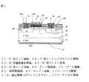
図1は、本発明によって製造される、炭化珪素半導体装置の実施例の断面構造図を示している。図に示すように、高濃度P+型SiC基板10上にP−型SiCエピタキシャル領域20が形成されている。そしてエピタキシャル領域20の所定領域には、N−型電界緩和領域30が形成される。N−型電界緩和領域30を含むP−型SiCエピタキシャル領域20上、すなわち、N−型電界緩和領域30を含む炭化珪素半導体基板の主表面上には、N−型のチャネル領域130を部分として含むN−型エピタキシャル層が形成され、チャネル領域130に接続されて、N+型ソース領域50が配置される。また、N−型電界緩和領域30内にはN+型ドレイン領域40が配置される。
【0014】
そしてN−型エピタキシャル層(その一部分がチャネル領域130である)の上にはゲート絶縁膜60を介してゲート電極70が配置され、ゲート電極70は層間絶縁膜80にて覆われている。N+型ドレイン領域40、N+型ソース領域50のそれぞれに接するようにドレイン電極90、ソース電極100が形成されるとともに、P+型SiC基板10の裏面にも電極110(ボディコンタクト)が形成されている。
【0015】
この実施例の炭化珪素半導体装置の動作について説明する。
【0016】
ソース電極100と裏面電極110を接地させてドレイン電極90に電圧を印加した状態で、ゲート電極70に正の電圧が印加されると、ゲート絶縁膜60の下にチャネルが形成され、ドレイン電極90からソース電極100へと電流を流すことが可能となる。
【0017】
また、ゲート電極70に印加された電圧を取り去ることによってドレイン電極90とソース電極100との間は電気的に絶縁され、オフ状態となる。
【0018】
特に、オフ状態でドレイン電極90に高い電圧が印加された時は、蓄積型チャネル領域130に電界緩和領域30と重なった不純物濃度の大きい領域が存在しない(後述の製造方法の説明参照)ため、ゲート電極70端下のゲート絶縁膜60が破壊することがない。すなわち、オフ状態でドレイン電極90に高い電圧が印加されると、N−型電界緩和領域30とP−型エピタキシャル領域20との接合に逆方向電圧が印加され、空乏層は電界緩和領域30内で縦方向と横方向に2次元的に広がる。電界緩和領域30の厚さが十分に薄い場合には、横方向の空乏層が縦方向に伸びた空乏層の影響を受けて半導体表面での電界が低減される。半導体表面での電界はP−/N−接合とN−/N+接合でピークをもち、その間の電界緩和領域30内部では電界は、ピーク値より小さいほぼ−定の値をとる。デバイスの横方向の耐圧は表面での電界の積分値で与えられるから、RESURF MOSFET では、電圧降下を電界緩和領域30全体で受け持つことによってドレイン耐圧を向上させている。
【0019】
次に、本実施例で示した炭化珪素半導体装置の製造方法の一例を、図2から図7の各断面図を用いて説明する。
【0020】
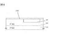
図2の工程では、P+型SiC基板10の上に例えば不純物濃度が1×10¹⁴〜1×1018cm−3、厚さが1〜100μmのP−型SiCエピタキシャル領域20が形成されている。
【0021】
図3の工程では、エピタキシャル領域20に対して犠牲酸化を行いその犠牲酸化膜を除去した後に、マスク材150を用いて例えば100〜1000℃で窒素イオン160を例えば10kV〜2MVの加速電圧で多段注入し、N−型電界緩和領域30を形成する(第1の工程)。総ドーズ量は例えば1×10¹²〜1×10¹⁵/cm2である。もちろんN型不純物としては窒素の他に燐、ヒ素などを用いてもよい。
【0022】
図4の工程では、N−型電界緩和領域30を含むP−型エピタキシャル領域20の主表面上、すなわち、N−型電界緩和領域30を含む炭化珪素半導体基板の主表面上に、例えば不純物濃度が1×10¹⁵〜1×1017cm−3、厚さが10〜10000オングストロームのN−型エピタキシャル層(その一部分がチャネル領域130である)をエピタキシャル成長する(第2の工程)。このときの成長条件は、ソースガスとしてSiH4、C3H8、H2を用い、成長温度を例えば1600℃程度とする。このようにして形成されたチャネル領域130においては、均一な濃度で不純物がドーピングされているので、従来技術の場合とは異なり、不純物濃度が局所的大きい部分が存在しない。これが、本発明に係る炭化珪素半導体装置の製造方法とその製造方法によって製造される炭化珪素半導体装置の特徴である。
【0023】
なお、チャネル領域130は、チャネル領域130を部分として含むN−型エピタキシャル層とP−型エピタキシャル領域20との間のビルトインポテンシャルの差、及び該N−型エピタキシャル層とゲート電極70との間の仕事関数の差により生じた電位によって、完全に空乏化される。このN−型エピタキシャル層の厚さ及び不純物濃度は、ゲート電圧を印加しないオフ時に、このN−型エピタキシャル層、したがって、チャネル領域130が完全に空乏化するように設定される。
【0024】
図5の工程では、マスク材151を用いて、N−型エピタキシャル層(その一部分がチャネル領域130である)上の所定領域(マスク材151で覆われていない領域)を通して、例えば100〜1000℃で燐イオン161を例えば10kV〜1MVの加速電圧で多段注入し、N+型ドレイン領域40及びN+型ソース領域50を形成する(第3の工程)。総ドーズ量は例えば1×10¹²〜1×10¹⁶/cm2である。もちろんN型不純物としては燐の他に窒素、ヒ素などを用いてもよい。
【0025】
その後1000〜1800℃での熱処理を行い、注入した不純物を活性化させる。
【0026】
図6の工程では、ゲート絶縁膜60を1200℃程度での熱酸化により形成し次に例えば多結晶シリコンによりゲート電極70を形成する。次に層間絶縁膜80としてCVD酸化膜を堆積する。
【0027】
図7の工程では、層間絶縁膜80に対しN+型ドレイン領域40及びN+型ソース領域50のそれぞれの領域上にコンタクトホールを開孔し、それぞれの開孔部にドレイン電極90及びソース電極100を形成する。また、P+型基板10裏面に基板電極110として金属膜を蒸着し、例えば600〜1400℃程度で熱処理してオーミック電極として、図1に示す炭化珪素半導体装置が完成する。
【0028】
これらの結果次の効果が得られる。
【0029】
ゲート絶縁膜の下のエピタキシャル成長で形成した蓄積型チャネル領域130には、電界緩和領域30と重なった不純物濃度の大きい領域が存在しない。そのため、オフ時にソース-ドレイン間に高い電圧を印加しても、ゲート電極70端下のゲート絶縁膜60が破壊することなく、電界緩和領域30内に空乏層が伸びて、高ドレイン耐圧が得られる。
【0030】
また蓄積型チャネル領域130を用いているため、反転型チャネルを用いたトランジスタと比べて、チャネル移動度を大きくしてオン抵抗を向上(すなわち低下)させるとともに、低いゲート電圧でトランジスタをオン状態にスイッチングできる。
【0031】
〔参考例〕
図8は、本発明の参考例となる炭化珪素半導体装置の製造方法によって製造される、炭化珪素半導体装置の断面構造図を示している。
【0032】
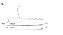
図8に示すように、P型SiC基板170上にN−型SiCエピタキシャル領域180が形成されている。そしてエピタキシャル領域180の所定領域には、P−型ベース領域140が形成される。P−型ベース領域140を含むN−型SiCエピタキシャル領域180上、すなわち、P−型ベース領域140を含む炭化珪素半導体基板の主表面上には、N−型エピタキシャル層(その一部分がチャネル領域131である)が形成され、このチャネル領域131に接続されて、N+型ドレイン領域41が配置される。また、P−型ベース領域140内にはN+型ソース領域51が配置される。
【0033】
そしてN−型エピタキシャル層(その一部分がチャネル領域131である)の上にはゲート絶縁膜61を介してゲート電極71が配置され、ゲート電極71は層間絶縁膜81にて覆われている。N+型ドレイン領域41、N+型ソース領域51それぞれに接するようにドレイン電極91、ソース電極101が形成されるとともに、P型SiC基板170の裏面にも電極111(ボディコンタクト)が形成されている。
【0034】
この参考例の炭化珪素半導体装置の動作について説明する。
【0035】
ソース電極101と裏面電極111を接地させてドレイン電極91に電圧を印加した状態で、ゲート電極71に正の電圧が印加されると、ゲート絶縁膜61の下にチャネルが形成され、ドレイン電極91からソース電極101へと電流を流すことが可能となる。
【0036】
また、ゲート電極71に印加された電圧を取り去ることによってドレイン電極91とソース電極101との間は電気的に絶縁され、オフ状態となる。
【0037】
特に、オフ状態でドレイン電極91に高い電圧が印加された時は、蓄積型チャネル領域131にN−型エピタキシャル領域180と重なった不純物濃度の大きい領域が存在しない(後述の製造方法の説明参照)ため、ゲート電極71端下のゲート絶縁膜61が破壊することなく、上記のようにN−型エピタキシャル領域180内に空乏層が伸びて、高ドレイン耐圧が得られる。
【0038】
次に、本参考例で示した炭化珪素半導体装置の製造方法の一例を、図9から図14の各断面図を用いて説明する。
【0039】
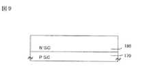
図9の工程では、P型SiC基板170の上に例えば不純物濃度が1×10¹⁴〜1×1018cm−3、厚さが1〜50μmのN−型SiCエピタキシャル領域180が形成されている。
【0040】
図10の工程では、エピタキシャル領域180に対して犠牲酸化を行いその犠牲酸化膜を除去した後に、マスク材152を用いて例えば100〜1000℃でアルミニウムイオン162を例えば10kV〜2MVの加速電圧で多段注入し、P−型ベース領域140を形成する(第1の工程)。総ドーズ量は例えば1×10¹²〜1×10¹⁵/cm2である。もちろんP型不純物としてはアルミニウムの他にほう素、ガリウムなどを用いてもよい。
【0041】
図11の工程では、P−型ベース領域140を含むN−型エピタキシャル領域180の主表面上、すなわち、P−型ベース領域140を含む炭化珪素半導体基板の主表面上に、例えば不純物濃度が1×10¹⁵〜1×1017cm−3、厚さが10〜10000オングストロームのN−型エピタキシャル層(その一部分がチャネル領域131である)をエピタキシャル成長する(第2の工程)。このときの成長条件は、ソースガスとしてSiH4、C3H8、H2を用い、成長温度を例えば1600℃程度とする。このようにして形成されたチャネル領域131においては、均一な濃度で不純物がドーピングされているので、不純物濃度が局所的に大きい部分が存在しない。これが、本参考例の炭化珪素半導体装置の製造方法とその製造方法によって製造される炭化珪素半導体装置の特徴である。
【0042】
なお、チャネル領域131は、チャネル領域131を部分として含むN−型エピタキシャル層とP−型ベース領域140との間のビルトインポテンシャルの差、及び該N−型エピタキシャル層とゲート電極71との間の仕事関数の差により生じた電位によって、完全に空乏化される。このN−型エピタキシャル層の厚さ及び不純物濃度は、ゲート電圧を印加しないオフ時にチャネル領域131が完全に空乏化するように設定される。
【0043】
図12の工程では、マスク材153を用いて、N−型エピタキシャル層(その一部分がチャネル領域131である)上から例えば100〜1000℃で燐イオン163を例えば10kV〜1MVの加速電圧で多段注入し、N+型ドレイン領域41及びN+型ソース領域51を形成する(第3の工程)。総ドーズ量は例えば1×10¹²〜1×10¹⁶/cm2である。もちろんN型不純物としては燐の他に窒素、ヒ素などを用いてもよい。
【0044】
その後1000〜1800℃での熱処理を行い、注入した不純物を活性化させる。
【0045】
図13の工程では、ゲート絶縁膜61を1200℃程度での熱酸化により形成し次に例えば多結晶シリコンによりゲート電極71を形成する。次に層間絶縁膜81としてCVD酸化膜を堆積する。
【0046】
図14の工程では、層間絶縁膜81に対しN+型ドレイン領域41及びN+型ソース領域51のそれぞれの領域上にコンタクトホールを開孔し、それぞれの開孔部にドレイン電極91及びソース電極101を形成する。また、P型基板170裏面に基板電極111として金属膜を蒸着し、例えば600〜1400℃程度で熱処理してオーミック電極として、図8に示す炭化珪素半導体装置が完成する。
【0047】
これらの結果次の効果が得られる。
【0048】
ゲート絶縁膜の下の蓄積型チャネル領域131にはN−型エピタキシャル領域180と重なった不純物濃度の大きい領域が存在しない。そのため、オフ時にソース-ドレイン間に高い電圧を印加しても、ゲート電極71端下のゲート絶縁膜61が破壊することなく、N−型エピタキシャル領域180内に空乏層が伸びて、高ドレイン耐圧が得られる。
【0049】
また蓄積型チャネル131を用いているため、反転型チャネルを用いたトランジスタと比べて、チャネル移動度を大きくしてオン抵抗を向上(すなわち低下)させるとともに、低いゲート電圧でトランジスタをオン状態にスイッチングできる。
【図面の簡単な説明】
【図1】 本発明第1の実施例を示す断面図である。
【図2】 本発明第1の実施例の製造工程を示す断面図である。
【図3】 本発明第1の実施例の製造工程を示す断面図である。
【図4】 本発明第1の実施例の製造工程を示す断面図である。
【図5】 本発明第1の実施例の製造工程を示す断面図である。
【図6】 本発明第1の実施例の製造工程を示す断面図である。
【図7】 本発明第1の実施例の製造工程を示す断面図である。
【図8】参考例を示す断面図である。
【図9】参考例の製造工程を示す断面図である。
【図10】参考例の製造工程を示す断面図である。
【図11】参考例の製造工程を示す断面図である。
【図12】参考例の製造工程を示す断面図である。
【図13】参考例の製造工程を示す断面図である。
【図14】参考例の製造工程を示す断面図である。
【図15】 従来技術による炭化珪素半導体装置を示す断面図である。
【符号の説明】
10…P+型SiC基板、20…P−型SiCエピタキシャル領域、30…N−型電界緩和領域、40、41…N+型ドレイン領域、50、51…N+型ソース領域、60、61…ゲート絶縁膜、70、71…ゲート電極、80、81…層間絶縁膜、90、91…ドレイン電極、100、101…ソース電極、110、111…裏面電極(ボディコンタクト)、120…N−型蓄積層、130、131…チャネル領域、140…ベース領域、150、151、152、153…マスク材、160、161、162、163…イオン、170…P型SiC基板、180…エピタキシャル領域、500…重複部分。[0001]
BACKGROUND OF THE INVENTION
[Non-Patent Document 1]
"Paper" High-Voltage Lateral RESURF MOSFET's on 4H-SiC, "IEEE Electron Device Lett., Vol. 21, pp. 356-358, 2000. K. Chatty, S. Banerjee, TP Chow, and RJ Gutmann"
[Non-Patent Document 2]
"Paper" The Planar 6H-SiC ACCUFET: A New High-Voltage Power MOSFET Structure, "IEEE Electron Device Lett., Vol. 18, pp. 589-591, 1997. PM Shenoy and BJ Baliga
The present invention relates to a method for manufacturing a silicon carbide semiconductor device and a silicon carbide semiconductor device manufactured by the method.
[0002]
[Prior art]
As an example of the silicon carbide semiconductor device, a silicon carbide RESURF MOSFET having an inversion channel is known as described in Non-Patent Document 1, for example. Further, in order to solve the problem of high on-resistance in the silicon carbide RESURF MOSFET having an inversion channel, for example, as described in Non-Patent
[0003]
The cross-sectional structure of the RESURF MOSFET using the storage channel is as shown in FIG.
[0004]
P in a region that operates as a lower channel of the
[0005]
[Problems to be solved by the invention]
However, the RESURF MOSFET using the conventional storage channel employs a manufacturing method in which the P− type
[0006]
The N− -
[0007]
The overlapping
[0008]
An object of the present invention is to provide a silicon carbide semiconductor device manufacturing method and a silicon carbide semiconductor device manufactured by the manufacturing method in which the gate insulating film does not cause dielectric breakdown even when the device is turned off. There is.
[0009]
[Means for Solving the Problems]
According to the present invention, the above object is achieved by configuring a method for manufacturing a silicon carbide semiconductor device, wherein an epitaxial layer including a storage channel region as a part is formed on a main surface of a silicon carbide semiconductor substrate. To do.
[0010]
【The invention's effect】
By carrying out the present invention, it is possible to provide a method for manufacturing a silicon carbide semiconductor device and a silicon carbide semiconductor device manufactured by the manufacturing method, in which the gate insulating film does not cause dielectric breakdown even when turned off.
[0011]
DETAILED DESCRIPTION OF THE INVENTION
Embodiments of the present invention will be described below with reference to the drawings. The polytype of silicon carbide (SiC) used in the following examplesand reference examples is typically 4H, but other polytypes such as 6H and 3C may be used.
[0012]
Moreover, it cannot be overemphasized that the deformation | transformation in the range which does not deviate from the main point of this invention is included.
[0013]
[Example 1]
FIG. 1 shows a sectional structural view of an embodiment of a silicon carbide semiconductor device manufactured according to the present invention. As shown in the figure, a P− type SiC
[0014]
A
[0015]
The operation of the silicon carbide semiconductor device of this embodiment will be described.
[0016]
When a positive voltage is applied to the
[0017]
In addition, by removing the voltage applied to the
[0018]
In particular, when a high voltage is applied to the
[0019]
Next, an example of a method for manufacturing the silicon carbide semiconductor device shown in the present embodiment will be described with reference to the cross-sectional views of FIGS.
[0020]
In the process of FIG. 2, for example, a P− type
[0021]
In the process of FIG. 3, after sacrificial oxidation is performed on the
[0022]
In the process of FIG. 4, for example, impurity concentration is formed on the main surface of P−
[0023]
The
[0024]
In the process of FIG. 5, the
[0025]
Thereafter, heat treatment is performed at 1000 to 1800 ° C. to activate the implanted impurities.
[0026]
In the process of FIG. 6, the
[0027]
In the process of FIG. 7, contact holes are formed in the respective regions of the N+ -
[0028]
As a result, the following effects can be obtained.
[0029]
In the
[0030]
In addition, since the
[0031]
[Reference example ]
8 shows areference example and made manufactured by the manufacturing method of the silicon carbide semiconductor device,cross-sectional structure viewof a silicon carbide semiconductor deviceof the present invention.
[0032]
As shown in FIG. 8, N− type
[0033]
A
[0034]
The operation of the silicon carbide semiconductor device of thisreference example will be described.
[0035]
When a positive voltage is applied to the
[0036]
Further, by removing the voltage applied to the
[0037]
In particular, when a high voltage is applied to the
[0038]
Next, an example of a method for manufacturing the silicon carbide semiconductor device shown in thisreference example will be described withreference to the cross-sectional views of FIGS.
[0039]
In the process of FIG. 9, for example, an N− type
[0040]
In the process of FIG. 10, after sacrificial oxidation is performed on the
[0041]
In the process of FIG. 11, for example, the impurity concentration is 1 on the main surface of N− type
[0042]
The
[0043]
In the process of FIG. 12, using the
[0044]
Thereafter, heat treatment is performed at 1000 to 1800 ° C. to activate the implanted impurities.
[0045]
In the process of FIG. 13, the
[0046]
In the process of FIG. 14, contact holes are opened in the respective regions of the N+ -
[0047]
As a result, the following effects can be obtained.
[0048]
In the
[0049]
In addition, since the
[Brief description of the drawings]
FIG. 1 is a cross-sectional view showing a first embodiment of the present invention.
FIG. 2 is a cross-sectional view showing a manufacturing process of the first embodiment of the present invention.
FIG. 3 is a cross-sectional view showing the manufacturing process of the first embodiment of the present invention.
FIG. 4 is a cross-sectional view showing the manufacturing process of the first embodiment of the present invention.
FIG. 5 is a cross-sectional view showing the manufacturing process of the first embodiment of the present invention.
FIG. 6 is a cross-sectional view showing the manufacturing process of the first embodiment of the present invention.
FIG. 7 is a cross-sectional view showing the manufacturing process of the first embodiment of the present invention.
FIG. 8 is a cross-sectional view showing areference example .
FIG. 9 is a cross-sectional view showing a manufacturing process of areference example .
FIG. 10 is a cross-sectional view showing the manufacturing process of thereference example .
FIG. 11 is a cross-sectional view showing a manufacturing process of areference example .
FIG. 12 is a cross-sectional view showing the manufacturing process of thereference example .
FIG. 13 is a cross-sectional view showing a manufacturing process of areference example .
FIG. 14 is a cross-sectional view showing a manufacturing process of areference example .
FIG. 15 is a cross sectional view showing a silicon carbide semiconductor device according to a conventional technique.
[Explanation of symbols]
10 ...P + -type SiC substrate, 20 ... P- -type SiC epitaxial region, 30 ... N- -type electric field relaxing regions, 40, 41 ...N + -type drain region, 50 and 51 ...N + -
Claims (2)
Translated fromJapanese前記炭化珪素半導体基板の主表面上に形成される前記炭化珪素半導体基板とは異なる導電型のソース領域と、
前記炭化珪素半導体基板の主表面上に前記ソース領域と離間した位置に形成される前記ソース領域と同じ導電型の電界緩和領域と、
該電界緩和領域の主表面に形成される前記ソース領域と同じ導電型のドレイン領域と、
該ドレイン領域及び前記ソース領域と接続して前記炭化珪素半導体基板の主表面上に形成される前記ソース領域と同じ導電型のチャネル領域と、
該チャネル領域上にゲート絶縁膜を介して形成されるゲート電極と、
を具備した炭化珪素半導体装置の製造方法において、
前記炭化珪素半導体基板の主表面上の所定領域に、前記電界緩和領域を形成する第1の工程と、
前記第1の工程で形成された前記電界緩和領域を含む前記炭化珪素半導体基板の主表面上に、前記チャネル領域を部分として含む炭化珪素エピタキシャル層を形成する第2の工程と、
前記第2の工程で形成された前記炭化珪素エピタキシャル層上の所定領域を通して不純物を導入することによって、前記第1の工程で形成された前記電界緩和領域内及び前記第2の工程で形成された前記炭化珪素エピタキシャル層内に、前記ドレイン領域を形成する第3の工程と、
を備えることを特徴とする炭化珪素半導体装置の製造方法。A silicon carbide semiconductor substrate having a predetermined conductivity type;
A source regionof a conductivity type different from that of the silicon carbide semiconductor substrate is formedon the main surface ofthe silicon carbide semiconductor substrate,
An electric field relaxation region of the same conductivity type as the source regionformed on the main surface of the silicon carbide semiconductor substrate at a position spaced from the source region;
Andthe source region and the drain region of the same conductivity type formed on themain surface of the field relaxation region,
And said drain regionandsaid source region same conductivity type as the channel region and formedon the main surface ofthe source region andthe silicon carbide semiconductor substrate are connected,
A gate electrode formed on the channel region via a gate insulating film;
In a method for manufacturing a silicon carbide semiconductor device comprising:
A first step of forming the electric field relaxation region in a predetermined regionon the main surface of the silicon carbide semiconductor substrate;
A second step of forming a silicon carbide epitaxial layer including the channel region as a part on a main surface of the silicon carbide semiconductor substrate including the electric field relaxation region formed in the first step;
By introducing impurities through a predetermined region on the silicon carbide epitaxial layer formed in the second step, the impurity is formed in the electric field relaxation region formed in the first step and in the second step. A third step of forming the drain region in the silicon carbide epitaxial layer;
The method of manufacturing a silicon carbide semiconductor device characterized by obtainingBei a.
前記炭化珪素半導体基板の主表面上に形成される前記炭化珪素半導体基板とは異なる導電型のソース領域と、A source region of a conductivity type different from that of the silicon carbide semiconductor substrate formed on the main surface of the silicon carbide semiconductor substrate;
前記炭化珪素半導体基板の主表面上に前記ソース領域と離間した位置に形成される前記ソース領域と同じ導電型の電界緩和領域と、An electric field relaxation region of the same conductivity type as the source region formed on the main surface of the silicon carbide semiconductor substrate at a position spaced from the source region;
該電界緩和領域の主表面に形成される前記ソース領域と同じ導電型のドレイン領域と、A drain region of the same conductivity type as the source region formed on the main surface of the electric field relaxation region;
該ドレイン領域及び前記ソース領域と接続して前記炭化珪素半導体基板の主表面上に形成される前記ソース領域と同じ導電型のチャネル領域と、A channel region of the same conductivity type as the source region formed on the main surface of the silicon carbide semiconductor substrate connected to the drain region and the source region;
該チャネル領域上にゲート絶縁膜を介して形成されるゲート電極と、A gate electrode formed on the channel region via a gate insulating film;
を具備した炭化珪素半導体装置であって、A silicon carbide semiconductor device comprising:
前記電界緩和領域を含む前記炭化珪素半導体基板の主表面上に、前記チャネル領域を部分として含む不純物濃度が均一な炭化珪素エピタキシャル層が形成され、A silicon carbide epitaxial layer having a uniform impurity concentration including the channel region as a part is formed on the main surface of the silicon carbide semiconductor substrate including the electric field relaxation region,
前記電界緩和領域内及び前記炭化珪素エピタキシャル層内に前記ドレイン領域が形成されたことを特徴とする炭化珪素半導体装置。The silicon carbide semiconductor device, wherein the drain region is formed in the electric field relaxation region and in the silicon carbide epitaxial layer.
Priority Applications (1)
| Application Number | Priority Date | Filing Date | Title |
|---|---|---|---|
| JP2002271433AJP3941641B2 (en) | 2002-09-18 | 2002-09-18 | Silicon carbide semiconductor device manufacturing method and silicon carbide semiconductor device manufactured by the manufacturing method |
Applications Claiming Priority (1)
| Application Number | Priority Date | Filing Date | Title |
|---|---|---|---|
| JP2002271433AJP3941641B2 (en) | 2002-09-18 | 2002-09-18 | Silicon carbide semiconductor device manufacturing method and silicon carbide semiconductor device manufactured by the manufacturing method |
Publications (2)
| Publication Number | Publication Date |
|---|---|
| JP2004111614A JP2004111614A (en) | 2004-04-08 |
| JP3941641B2true JP3941641B2 (en) | 2007-07-04 |
Family
ID=32268745
Family Applications (1)
| Application Number | Title | Priority Date | Filing Date |
|---|---|---|---|
| JP2002271433AExpired - Fee RelatedJP3941641B2 (en) | 2002-09-18 | 2002-09-18 | Silicon carbide semiconductor device manufacturing method and silicon carbide semiconductor device manufactured by the manufacturing method |
Country Status (1)
| Country | Link |
|---|---|
| JP (1) | JP3941641B2 (en) |
Cited By (1)
| Publication number | Priority date | Publication date | Assignee | Title |
|---|---|---|---|---|
| CN102668094A (en)* | 2010-10-29 | 2012-09-12 | 松下电器产业株式会社 | Semiconductor element and semiconductor device |
Families Citing this family (7)
| Publication number | Priority date | Publication date | Assignee | Title |
|---|---|---|---|---|
| WO2010125819A1 (en) | 2009-04-30 | 2010-11-04 | パナソニック株式会社 | Semiconductor element, semiconductor device, and power converter |
| WO2011021361A1 (en)* | 2009-08-19 | 2011-02-24 | パナソニック株式会社 | Semiconductor element, semiconductor device, and electric power converter |
| JP5623898B2 (en)* | 2010-12-21 | 2014-11-12 | ルネサスエレクトロニクス株式会社 | Semiconductor device and manufacturing method thereof |
| JP6228428B2 (en)* | 2013-10-30 | 2017-11-08 | ルネサスエレクトロニクス株式会社 | Semiconductor device |
| RU2719569C1 (en)* | 2017-02-14 | 2020-04-21 | Ниссан Мотор Ко., Лтд. | Semiconductor device and method of its manufacturing |
| FR3086101B1 (en) | 2018-09-17 | 2022-07-08 | Ion Beam Services | DEVICE FOR ENHANCING CARRIER MOBILITY IN A MOSFET CHANNEL ON SILICON CARBIDE |
| KR20230093791A (en)* | 2021-12-20 | 2023-06-27 | 한국전기연구원 | Implementation of SiC Semiconductor Devices On SiC Insulation or Semi-insulation Substrate And Manufacturing Methods of The Same |
- 2002
- 2002-09-18JPJP2002271433Apatent/JP3941641B2/ennot_activeExpired - Fee Related
Cited By (3)
| Publication number | Priority date | Publication date | Assignee | Title |
|---|---|---|---|---|
| CN102668094A (en)* | 2010-10-29 | 2012-09-12 | 松下电器产业株式会社 | Semiconductor element and semiconductor device |
| US8809871B2 (en) | 2010-10-29 | 2014-08-19 | Panasonic Corporation | Semiconductor element and semiconductor device |
| CN102668094B (en)* | 2010-10-29 | 2015-02-25 | 松下电器产业株式会社 | Semiconductor element and semiconductor device |
Also Published As
| Publication number | Publication date |
|---|---|
| JP2004111614A (en) | 2004-04-08 |
Similar Documents
| Publication | Publication Date | Title |
|---|---|---|
| US9142663B2 (en) | Silicon carbide devices having smooth channels | |
| JP5603008B2 (en) | Method for forming SiCMOSFET having large inversion layer mobility | |
| US6429041B1 (en) | Methods of fabricating silicon carbide inversion channel devices without the need to utilize P-type implantation | |
| US9876103B2 (en) | Semiconductor device and transistor cell having a diode region | |
| US7705362B2 (en) | Silicon carbide devices with hybrid well regions | |
| US8288220B2 (en) | Methods of forming semiconductor devices including epitaxial layers and related structures | |
| US7381992B2 (en) | Silicon carbide power devices with self-aligned source and well regions | |
| JP2000106371A (en) | Method for manufacturing silicon carbide semiconductor device | |
| JP2002203967A (en) | Semiconductor element | |
| JP2012114104A (en) | Storage insulation gate type field effect transistor | |
| JP3939583B2 (en) | Method for manufacturing field effect transistor | |
| JP3941641B2 (en) | Silicon carbide semiconductor device manufacturing method and silicon carbide semiconductor device manufactured by the manufacturing method | |
| JP3496509B2 (en) | Method for manufacturing silicon carbide semiconductor device | |
| US6150671A (en) | Semiconductor device having high channel mobility and a high breakdown voltage for high power applications | |
| JP2005353877A (en) | Semiconductor device | |
| JP4765175B2 (en) | Method for manufacturing silicon carbide semiconductor device | |
| EP0890183B1 (en) | A FIELD EFFECT TRANSISTOR OF SiC AND A METHOD FOR PRODUCTION THEREOF | |
| JP2004253427A (en) | Silicon carbide semiconductor device |
Legal Events
| Date | Code | Title | Description |
|---|---|---|---|
| A621 | Written request for application examination | Free format text:JAPANESE INTERMEDIATE CODE: A621 Effective date:20041222 | |
| A977 | Report on retrieval | Free format text:JAPANESE INTERMEDIATE CODE: A971007 Effective date:20061122 | |
| A131 | Notification of reasons for refusal | Free format text:JAPANESE INTERMEDIATE CODE: A131 Effective date:20061128 | |
| A521 | Request for written amendment filed | Free format text:JAPANESE INTERMEDIATE CODE: A523 Effective date:20070126 | |
| RD02 | Notification of acceptance of power of attorney | Free format text:JAPANESE INTERMEDIATE CODE: A7422 Effective date:20070126 | |
| TRDD | Decision of grant or rejection written | ||
| A01 | Written decision to grant a patent or to grant a registration (utility model) | Free format text:JAPANESE INTERMEDIATE CODE: A01 Effective date:20070313 | |
| A61 | First payment of annual fees (during grant procedure) | Free format text:JAPANESE INTERMEDIATE CODE: A61 Effective date:20070326 | |
| R150 | Certificate of patent or registration of utility model | Ref document number:3941641 Country of ref document:JP Free format text:JAPANESE INTERMEDIATE CODE: R150 Free format text:JAPANESE INTERMEDIATE CODE: R150 | |
| FPAY | Renewal fee payment (event date is renewal date of database) | Free format text:PAYMENT UNTIL: 20110413 Year of fee payment:4 | |
| FPAY | Renewal fee payment (event date is renewal date of database) | Free format text:PAYMENT UNTIL: 20120413 Year of fee payment:5 | |
| FPAY | Renewal fee payment (event date is renewal date of database) | Free format text:PAYMENT UNTIL: 20130413 Year of fee payment:6 | |
| FPAY | Renewal fee payment (event date is renewal date of database) | Free format text:PAYMENT UNTIL: 20130413 Year of fee payment:6 | |
| FPAY | Renewal fee payment (event date is renewal date of database) | Free format text:PAYMENT UNTIL: 20140413 Year of fee payment:7 | |
| LAPS | Cancellation because of no payment of annual fees |