JP3936830B2 - Semiconductor device - Google Patents
Semiconductor deviceDownload PDFInfo
- Publication number
- JP3936830B2 JP3936830B2JP2000143424AJP2000143424AJP3936830B2JP 3936830 B2JP3936830 B2JP 3936830B2JP 2000143424 AJP2000143424 AJP 2000143424AJP 2000143424 AJP2000143424 AJP 2000143424AJP 3936830 B2JP3936830 B2JP 3936830B2
- Authority
- JP
- Japan
- Prior art keywords
- region
- insulating film
- semiconductor
- layer
- gate
- Prior art date
- Legal status (The legal status is an assumption and is not a legal conclusion. Google has not performed a legal analysis and makes no representation as to the accuracy of the status listed.)
- Expired - Fee Related
Links
Images


Landscapes
- Non-Volatile Memory (AREA)
- Thin Film Transistor (AREA)
- Dram (AREA)
- Memory System (AREA)
- Semiconductor Memories (AREA)
Description
Translated fromJapanese【0001】
【発明の属する技術分野】
本願発明は、大規模集積化が可能な半導体装置、並びにこれを用いた半導体記憶装置に関するものである。更には、本願発明はこの半導体装置あるいは半導体記憶装置の製造方法に関するものである。
【0002】
【従来の技術】
現在の代表的な集積化半導体装置であるシリコン基板を用いたULSIのトランジスタの主要部は、図1に示すような断面構造を有している。CMOSで用いているトランジスタは、半導体基板100に、ソース、ドレインとして高濃度に不純物をドーピングした拡散層(200、300)を電極領域として用いた絶縁ゲート型トランジスタを用いて構成されている。尚、符号500はゲート電極である。
【0003】
絶縁ゲート型トランジスタ、その代表例たるMOSFETは、制御するチャネルのキャリアが、チャネルとなる基板と反対導伝型キャリアのみを用いる。このことから絶縁ゲート型トランジスタはユニポーラデバイスと呼ばれている。ユニポーラデバイスでは、ソース、ドレインといった電極が基板100と電気的に分離されていることがデバイス動作上の基本となる。通常、拡散層と基板は、異なる導伝型を用いることでPN接合を形成し、接合のビルトイン障壁によってそれぞれの電極と基板を電気的に分離してきた。しかし、ソース、ドレイン間の距離が短くなるに従い、この障壁のみでは良好な分離を果たすことができず、基板へのリーク、そしてソース、ドレイン間にリーク電流を生じる問題が顕著になってきた。こうした電流リークは、ドレイン電界の影響がソース側まで及ぶため生じるものと考えられている。そのため、リークを抑制するには、前記不純物拡散層200、300の深さを小さく(浅く)することで、ソース、ドレインの対向面積を小さくすることが有効である。この深さは図1にXjとして示されている。しかし、拡散層深さを浅くすると、拡散層の抵抗が増大し、トランジスタの電流駆動力を低下させる問題が生じてきている。
【0004】
また、これとは異なるアプローチとして、拡散層電極周囲を絶縁膜層で囲み、電極とチャネル(基板)の間にリークにたいするバリアを設けることが考えられている。また、日本国公開特許公報、特開平10―200001に見られる構造は、拡散層電極とチャネル間のみではなく、さらに、チャネル部にも多層の絶縁膜層を差し挟んだ構造になっている。但し、後者では、その製造工程上、チャネル部が単結晶ではなく多結晶により構成された、一種の薄膜トランジスタ(TFT:Thin Film Transistor)と呼ばれる構造とみることができる。これらの構造では、拡散層抵抗を増大させることなくリークを抑制することは可能であるが、絶縁膜を介してチャネル電流を流すことが必要となるため、電流駆動力を低下させる問題が生じてくる。
【0005】
浅接合化による電極抵抗増大を解決する方法として、ソース、ドレインに金属材を用いることが提案されている。一般には、電極と基板との分離がPN接合ではなく、金属と半導体接触部に形成されるショットキー接合によりなされているため、ショットキーバリア ソース・ドレイン MOSFET(SB-MOSFET)と呼ばれている。これらの構造については、例えば、アプライド、フィジックス、レター、65巻、618頁から620頁(Appl. Phys. Lett. 65(5),pp.618-620,1994) において、Tucker等により検討されている。また、実際の試作としては、エス、ピー、アイ、イー、コンファレンス、オン、マイクロエレクトロニック、デバイス、テクノロジー、ツー、1998年7月、エス、ピー、アイ、イー、3506巻、230頁から233頁(Part of the SPIE Conference on Microelectronic Device Technology II, SPIE vol. 3506, pp.230-233)においてWang等の報告がみられる。これらの報告では、ショットキー接合を用いた効果として、ソース、ドレイン間の距離を小さくした短チャネル構造でも、接合間のリークを有効に抑えることができることが明らかになってきた。しかし、PN接合に比べ良好な接合を形成することが困難なため、基板との間のリークが増大してしまい、ソース、ドレイン間のリークの低減効果を打ち消してしまったり、接合のオン抵抗が高いため、結局、電極抵抗の低減効果も見えなくなっている。
【0006】
又、半導体記憶装置に用いるゲインセルとしては、例えば書き込み用にp型MOS、読み取り用にn型MOSを用いた例が、Shoji ShukuriらによるIEDM92、1006−1008に見られる。
【0007】
【発明が解決しようとする課題】
本願の第1の目的は、リーク電流の極めて低い絶縁ゲート型電界効果型トランジスタを提供するものである。即ち、本願発明は、短チャネル化を進めるために増大してきたリーク電流を低減するために行われてきた上記の様々な対策により生じる駆動力の低下を抑制するものである。
【0008】
本願の第2の目的は、記憶特性の良好な半導体記憶装置を提供するものである。前記のリーク電流の低い絶縁ゲート型電界効果型トランジスタを用いて、リーク電流の少ない3端子スイッチング素子を得ることができる。従って、このことは、特に、半導体記憶素子を形成する上で有効なものとなる。
【0009】
本願の更に別な目的は、前記の半導体装置、あるいは半導体記憶装置等を提供する為の製造方法を提供するものである。
【0010】
【課題を解決するための手段】
先ず、ここでは発明の理解を容易にする為に、本願発明の発明思想の骨子を説明する。そして、発明の実施の形態の欄に更に詳細な発明の諸形態を説明する。
【0011】
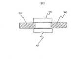
ショットキー接合では、接合を挟む異なる物質の界面ができることにより、PN接合に比べ接合のリークが多くなっている。従来の図1に示した構造をもとにSB−MOSFETを形成すると、スイッチングに用いているのは、ゲート端部の接合のみで、底面等はスイッチング動作上は不要であるにも関わらず、接合の面積のほとんどを占めることになるため、この底面がリークの主要発生源となっている。こうした不要なリークを抑えるには、図2に模式的に示すように、ゲート500、510により、両側からチャネル101を挟む構造にし、不要な接合をなくし、接合をチャネル方向のみとすることが有効である。本発明における具体的構造については、実施形態の説明において、製造方法をもとに詳細に述べる。この構造では、スイッチングに必要なゲート端部のみに接合が設けられており、不要な接合によるリークを生じることがない。
【0012】
さらにリークを抑えるため、金属と半導体の間にリークを妨げる障壁となる絶縁層を挟む構造をとっている。これは、拡散層電極周辺を絶縁膜で囲む構造を適用したものである。
【0013】
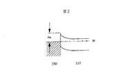
図3は通例のショトッキー接合を説明する為のバンド構造図である。図3には、金属部350と半導体部110の接合領域、及び価電子帯の上端、伝導帯の下端、およびフェルミ準位Efが示される。図4は本願発明で用いる接合を説明する為のバンド構造図である。図4の構成では図3の構造に絶縁物層931が設けられている。
【0014】
すなわち、ショットキー接合では図3のバンド図に示したように、ショットキーバリアと呼ばれる障壁Pmによりリーク電流を抑えている。そこに、図4にみられるように、Pmに比べより大きな障壁高さPiを持った絶縁膜をはさむことで、金属側から半導体側に通り抜けるキャリアを低減することができる。このショットキー接合に代えて絶縁層を挟んだ構造の接合は、MIS接合(MetalInsulation Junction)として知られている。この例は、例えば、Sze著のフィジックス オブ セミコンダクタ デバイシーズ、第2版、ジョンウィリー アンド サンズ(Physics of Semiconductor Devices, second edition, JOHN WILEY & SONS)の540頁から553頁に記述されている。このように高い障壁高さPiを持つ絶縁層を挟んでも、絶縁層の膜厚を極めて薄くすることで、トンネル現象を促進できることから、接合のスイッチング動作させることができる。
【0015】
一般に、この絶縁膜をトンネル現象により通り抜けるキャリアは、障壁高さ、膜厚、およびキャリアのエネルギーに依存している。デバイス構造としては、金属材と絶縁膜間の障壁高さ、絶縁膜の膜厚、非平衡状態のポテンシャル分布を制御することができる。
【0016】
本発明の構造では、さらに、縦形のチャネル配置をとることにより、平面面積を増やすことなくチャネル長の大きなデバイスを形成している。これにより、短チャネル化によるリーク電流の増大を抑えることができる。さらに、ゲートを両側に配置することで、より有効に電界効果を活かすことができるようになる。この縦形構造をとることで、従来困難であった非対称型系のトランジスタを容易に形成することができるようになっている。そのため、絶縁膜による障壁は片側のみに形成することができており、駆動力の低下を抑制することができている。
【0017】
これらの効果を有効に引き出すことで、リーク電流を極めて低く抑制できる3端子トランジスタ構造を得ることができる。また、この低リーク特性は、記憶保持および、書き込み、読み出し動作に優れた半導体記憶装置を形成する上で有効であることを、実施例をもとに説明する。
【0018】
【発明の実施の形態】
本願発明の実施の形態を具体的に説明するに先だって、本願発明の主な諸形態の概略を列挙し、説明する。
【0019】
本願に係る半導体装置
本願発明の半導体装置の代表的な第1の形態は、第1の導電領域、第1の絶縁膜、第1の半導体領域、および第2の導電領域とを有する半導体領域と、少なくとも前記第1の半導体領域に設けた第2の絶縁膜と、前記第2の絶縁膜の膜面に設けられた第3の導電領域と、を有する半導体装置である。
【0020】
本発明は新規なスイッチ素子を提供することが出来る。そして、後述するように、新規な半導体記憶装置のスイッチ部として極めて有用である。又、本発明の構造は通例の半導体分野の製造方法によって製造することが出来る。従って、本発明の半導体装置は極めて安価に提供することが出来る。
【0021】
本願発明の半導体装置の代表的な第2の形態は、第1の導電領域、第1の絶縁膜、第1の半導体領域、および第2の導電領域とが積層された半導体積層領域と、少なくとも前記第1の半導体領域の前記半導体積層領域の積層方向とは交差する側面に設けた第2の絶縁膜と、前記第2の絶縁膜の膜面に設けられた第3の導電領域と、を有する半導体装置である。
【0022】
上記の諸形態では、第1の導電領域、第1の絶縁膜、第1の半導体領域、および第2の導電領域とを有する半導体領域が、絶縁ゲート型電界効果型トランジスタの電荷移送手段及び電荷移送領域を構成する。前記第1の半導体領域は、いわゆるチャネル領域に、前記第1及び第2の導電領域はソースあるいはドレインのいずれかに相当する。これらをソースあるいはドレインと称するかはその動作状態に依存する相違にすぎない。そして、前記第1の導電領域、第1の絶縁膜、第1の半導体領域の半導体領域が、図4を用いて説明したバンド構造を有する積層体である。本形態において、前記第1の絶縁膜を設けた点がわけても重要な点である。
【0023】
この第1の絶縁膜は、通例第1の導電領域として用いる金属の酸化物、酸化度の低い酸化物、窒化物、窒化度の低い窒化物、シリコンと金属の酸化物、シリコンと金属の窒化物、あるいはこれらの内の少なくとも2者を含む絶縁物などが用いられる。より具体的に、これらの金属とこれに適した絶縁物の諸例をかかげれば、耐熱金属とその酸化物、窒化物、あるいはシリサイドが好適である。更に、具体例をかかげれば、金属あるいは金属相当の導電体として、チタン、チタンシリサイド、タングステン、タングステン・シリサイド、コバルト、コバルト・シリサイド、白金、白金シリサイド、ニッケル、ニッケル・シリサイドなどをあげることが出来る。絶縁物の具体例としては、シリコン酸化物、シリコン窒化物などが代表例である。更に、絶縁物の例としては、前記各種金属あるいは耐熱金属の酸化物、あるいは窒化物などをあげることが出来る。チタンとチタン・シリサイドなどは熱的に安定であり、好ましい例である。シリコン酸化物、あるいはシリサイド等は通例の半導体分野に製造工程に多く用いられている材料であり、本願発明の半導体装置、半導体記憶装置の製造に好都合である。勿論、その要求によって、前記例示した金属および絶縁物を適宜組み合わせて用いることが出来る。
【0024】
そして、これらの絶縁膜が当該接合におけるトンネル効果を奏する厚さとなす。この絶縁膜の厚さ例をかかげれば、シリコン酸化物の場合、3nm以下、好ましくは1nmより2nm程度が多用される。
【0025】
尚、第1の導電領域と第1の絶縁膜の具体例について言及したが、これらの諸例は、以下本願明細書に記載される発明の諸形態、実施の諸形態に対しても適用できるものであることは言うまでもない。
【0026】
第3の形態は、ソースとドレインとゲート電極およびチャネル領域を有する絶縁ゲート型電界効果トランジスタにおいて、ソースまたはドレイン電極となる第1の導電領域上に第1の絶縁物層を有し、前記第1の絶縁膜の上部にチャネル領域となる半導体材料層を有し、前記半導体層上にドレインまたはソース電極となる第2の導電領域を有し、前記チャネル領域側面に第2の絶縁膜層を有し、前記第2の絶縁膜層を介して電界効果を前記チャネル領域におよぼすゲート電極を有することを特徴とする半導体装置と言うことが出来る。
【0027】
上記の各部の材料の選択によって、下記の諸形態が考えられる。
【0028】
本願の第4の形態は、前記の諸形態における第1の導電領域が金属材料により形成されているものである。
【0029】
更に、本願の第5の形態は、前記の諸形態における前記第1の導電領域が高濃度に不純物をドーピングすることで実質的に金属化された半導体材料により形成されているものである。
【0030】
更に、本願の第6の形態は、第2の導電領域が高濃度に不純物をドーピングすることで実質的に金属化された半導体材料により形成されているものである。
【0031】
本願発明においては、前記の各導電領域を組み合わせ用いることが出来る。即ち、本願の第7の形態は、前記第1の導電領域が金属材料あるいは高濃度に不純物をドーピングすることで金属化された半導体材料により形成され、前記第2の導電領域が高濃度に不純物をドーピングすることで金属化された半導体材料により形成されているものである。
【0032】
本願の第8の形態は、前記第1の導電領域が高濃度に不純物をドーピングすることで金属化された半導体材料により形成され、前記第2の導電領域が金属材料あるいは高濃度に不純物をドーピングすることで金属化された半導体材料により形成されているものである。
【0033】
前記半導体材料を母材とした金属化に必要な不純物のドープ量は、通例の半導体分野における範囲を用いて十分である。シリコンに対してのドープ量は通例、1020cm―3程度以上の範囲である。
【0034】
これらのドープ量に関する諸例は、本願明細書に記載される発明の諸形態、実施の諸形態に対しても適用できるものであることは言うまでもない。
【0035】
尚、本願発明の半導体装置において、第1の導電領域および第2の導電領域に挟まれた半導体領域が、電界効果型トランジスタの電荷移送領域、即ち、いわゆるチャネル領域を構成する。従って、この意味において、本願発明においては、電荷移送領域は、半導体領域とトンネル絶縁膜との双方で電荷移送領域を構成することとなる。従って、この意図を示す形態の例は次のように言うことが出来る。
【0036】
本願発明の第9の形態は、第1の導電領域、第1の絶縁膜、第1の半導体領域、および第2の導電領域とを有する半導体領域と、前記第2の半導体領域の前記半導体領域の積層方向とは交差する側面に設けた第2の絶縁膜と、前記第2の絶縁膜の膜面に設けられた第3の導電領域と、を有し、且つ前記第1あるいは第2の導電領域の内のいずれかが高濃度に不純物をドーピングした多結晶シリコンにより形成され、前記第1あるいは第2の導電領域の内の他方のいずれかが金属により形成され、前記第1の導電領域から第2の導電領域に流れる電流経路に、シリコンおよびトンネル絶縁膜が配置されている半導体装置である。
【0037】
上記の形態をより具体的に示せば、本例はソースが高濃度不純物をドーピングした多結晶シリコンにより形成され、ドレインが金属により形成され、ソースからドレインに流れる電流経路において、シリコンとトンネル絶縁膜が配置されている半導体装置と言うことが出来る。
【0038】
これまで述べてきた本願発明の諸形態の半導体装置の更なる実用上の形態を示せば、当該半導体装置のスイッチングがオフ状態においてチャネル部のキャリアが空乏化されている半導体装置であると言うことが出来る。半導体記憶装置
次に、これまで説明してきた半導体装置、即ち絶縁ゲート型電界効果型トランジスタを用いた半導体記憶装置について説明する。
【0039】
当該半導体記憶装置の代表的な第10の形態は、前述の本願発明の諸半導体装置のいずれかを情報書き込み装置とし、前記第1の導電領域を電荷保持部とし、この電荷保持部に電気的に接続された情報読み出し素子を有する半導体記憶装置である。
【0040】
そして、前記情報読み出し素子が電界効果型トランジスタであるのが、より実際的な半導体記憶装置である。
【0041】
そして、この形態の半導体記憶装置において、前記電荷保持部が絶縁膜で囲まれ、前記電荷保持部に保持した電荷量により情報を記憶することが、より好ましい。
【0042】
このように、本願発明の半導体装置の諸形態を情報書き込み手段として用いて半導体記憶装置を構成する場合、当該半導体記憶装置の電荷蓄積ノード側に、前記本願発明の係わる半導体装置のトンネル絶縁膜に接して設けられた導電領域を接続するのが好ましい。それは、蓄積電荷を確保するにとより好都合であるからである。勿論、当該半導体装置の第1および第2の導電領域のいずれを当該半導体記憶装置の電荷蓄積ノード側に設置しても、半導体記憶装置を提供できることは言うまでもない。
【0043】
又、本願発明の半導体装置の諸形態を情報書き込み手段として用いて半導体記憶装置を構成する場合、N型の絶縁ゲート型電界効果型トランジスタを横型の素子として配置し、P型の絶縁ゲート型電界効果型トランジスタとして本願に係るトンネル絶縁膜をい用いた縦型の素子として用いるのがより好都合である。
【0044】
本願発明の半導体記憶装置の代表的な第11の形態は、キャリアを移動せしめる第1の経路と、前記第1の経路の伝導性を変化させる電界を生成する電荷を蓄積する為の手段と、所望の電圧に対して所望の電荷を前記電荷を蓄積する為の手段に供給する手段とを、有し、且つ所望の電荷を前記電荷を蓄積する為の手段に供給する手段が、金属性電極部、トンネル絶縁膜、および半導体領域とを有する接合を有することを特徴とすることである。
【0045】
言い換えれば、この形態は、本願発明に係る半導体装置なる電界効果型トランジスタ(T1)のソースまたはドレイン電極と、半導体基板上に形成された絶縁ゲート型電界効果型トランジスタ(T2)を有する半導体記憶装置において、T1のチャネルを介してT2のゲート電極に接続がなされている半導体記憶装置である。そして、トンネル絶縁膜を利用してスイッチ動作を行なうものである。前述の本願発明に係る半導体装置なる電界効果型トランジスタ(T1)は、少なくとも、導電領域―チャネル領域―トンネル絶縁膜―金属導電領域の積層構造を有する。ここで、導電領域、ないしは金属導電領域が、電界効果型トランジスタのソース、あるいはドレインに相当するものである。従って、前記T1とT2の接続は次の形態がある。
【0046】
(1)導電領域―半導体領域―トンネル絶縁膜―金属導電領域―T2のゲート、
(2)金属導電領域―トンネル絶縁膜―半導体領域―導電領域―T2のゲート
そして、この場合、実際の構造においては、前記(1)における金属導電領域―T2のゲート、あるいは前記(2)における導電領域―T2のゲートは同一層で形成し、その両者の役割を兼ねることが、より実際的である。
【0047】
本願発明の半導体記憶装置の動作を要約すれば、前記第11の形態にある電荷によって情報を記憶させた半導体記憶装置において、書き込み素子T1を介して電荷を出し入れし、T2を電荷の保持状況を読み出す読み出し素子としていると言うことが出来る。
【0048】
本願発明の半導体装置の、第12の形態は、半導体基板と、当該半導体基板に相対して設けられた第1の不純物領域及び第2の不純物領域と、少なくとも前記第1不純物領域及び第2の不純物領域に挟まれた第1の半導体領域を覆う第1の絶縁膜と、当該第1の絶縁膜の上部に設けられた第1の導電領域、第2の絶縁膜、第2の半導体領域、および第2の導電領域とを有する半導体領域と、前記第2の半導体領域の前記半導体領域の積層方向とは交差する側面に設けた第3の絶縁膜と、前記第3の絶縁膜の膜面に設けられた第3の導電領域と、を有する半導体装置である。
【0049】
本形態は、スイッチ素子部を構成する電界効果型トランジスタ部が、そのチャネル領域が当該半導体記憶装置の基板に交差、ないしは実質的に直交する方向に構成されている。これはいわゆる縦形半導体装置と称されている形態である。従って、この形態は装置の小型化に有利である。更に、前記第2の半導体領域の側壁が絶縁膜で覆われた構造を採用すれば、よりリーク電流の少ない半導体記憶装置を提供することが出来る。
【0050】
本願発明の主なその他の形態
本願の第13の形態は、前記第10の半導体装置において、書き込み素子のゲート電極配線と基板電位間に電位を安定化させる手段を有する集積半導体装置である。より具体的な要請は、電源が切れた場合においてもゲート電極と導電領域との間の相対的な電位関係が固定されていることである。この電位の安定化の為の手段の最も簡単で実用的なものは抵抗である。しかし、本要請に答えるには多くの回路を用いることが出来る。
【0051】
本願の第14の形態は、例えば、前記第11、ないしは前記第12の半導体記憶装置を少なくとも2つ用いた集積半導体装置において、読み出し素子T2が電気的に縦積みされた配置をとっている半導体装置である。
【0052】
本願の第15の形態は、例えば、前記の諸半導体記憶装置において、情報読み出し時に、書き込み素子T1のゲート電極電位を変えることなく、T2のソース、ドレイン電位を変化させることで、該ゲート電極と該ソース、ドレイン電極間の電位差変化を与えることで読み出し操作を行う半導体記憶装置である。
【0053】
前述したように、ゲート電位が固定される必要があることから、本願発明の半導体記憶装置においては、ゲート電位を固定し、ソースあるいはドレインの電位を変化させるのが好ましい。
【0054】
本願の第16の形態は、例えば、前述の諸半導体記憶装置において、情報読み出し時に、読み出し素子T2のゲート電極電位を変えることなく、ソース、ドレイン電位を変化させることで、該ゲート電極と該ソース、ドレイン電極間の電位差変化を与えることで読み出し操作を行う半導体記憶装置である。
【0055】
本願の第17の形態は、例えば、前記第11ないしは第12の半導体記憶装置を複数用いてアレイ状に配置し、基板上に形成された読み出し素子T2のソース、ドレイン電極に接続された配線層が直交するように平面配置されている半導体記憶装置である。
【0056】
本願の第18の形態は、本願に係わる半導体装置、ないしは半導体記憶装置、例えば前記第1、第2、あるいは第10、第11の半導体装置、ないしは半導体記憶装置が、SOI(Silicon On Insulator)基板上に形成されている集積化半導体装置である。基板に絶縁基板を用いることから、本願発明のリーク電流の抑制された半導体装置、ないしは半導体記憶装置の要請がより有効に機能する。
【0057】
本願の第19の形態は、上記集積半導体記憶装置において、書き込み素子のゲート電極配線と基板電位間に電力を消費することなく電位を安定化させる装置を有する集積半導体装置である。
【0058】
本願の第20の形態は、電界効果トランジスタによる書き込み装置と、該書き込み装置と異なる導電型をもった電界効果トランジスタによる読み出し装置を持つ半導体記憶装置である。
【0059】
本願の第21の形態は、例えば前記20の半導体記憶装置において、情報読み出し時に、書き込み素子のゲート電極に、電荷保持時に比べ書き込み素子のチャネルをよりオフ状態とする電位を加える半導体記憶装置である。
【0060】
本願の第22の形態は、例えば前記20の半導体記憶装置において、書き込まれる電位情報が少なくとも3つ以上の値を持つ集積半導体装置である。
【0061】
本願の第23の形態は、例えば前記21の半導体記憶装置において、保持された電荷情報を連続した電位として読み出す集積半導体装置である。 本願の第24の形態は、例えば前記12、あるいは前記20の半導体装置において、保持電荷とゲート電極電位により演算処理を行なわせる機能を付加した半導体装置である。
【0062】
本願の製造方法に係わる発明の主な形態
本願の製造方法に係わる第1の形態は、半導体基板上に第1の絶縁膜を形成する工程と、この絶縁膜上に金属層もしくは高濃度に不純物をドーピングすることで金属化された半導体材料層を形成する工程と、この金属材層もしくは金属化された半導体材料層の上部に第2の絶縁膜を形成する工程と、この第2の絶縁膜上に半導体材料層を形成する工程と、この半導体材料層の側面に第3の絶縁膜を形成する工程と、この第3の絶縁膜の側面に金属層もしくは高濃度に不純物をドーピングすることで金属化された半導体材料層を形成する工程を有する半導体装置の製造方法である。
【0063】
本願の製造方法に係わる第2の形態は、半導体基板上に第1の絶縁膜を形成する工程と、この第1の絶縁膜上に金属層もしくは高濃度に不純物をドーピングすることで金属化された半導体材料層を形成する工程と、前記金属材層もしくは金属化された半導体材料層の上部に第2の絶縁膜を形成する工程と、半導体材料をアモルファス状態で形成する工程と、このアモルファス状態の半導体材料層に所定の金属層を形成する工程と、加熱によって当該金属によって前記アモルファス状態の半導体材料層を結晶化する工程を有する半導体装置の製造方法である。
【0064】
この第2の半導体装置の製造方法は、わけても前記の縦型のトランジスタを製造するに当って有効である。即ち、本願発明の半導体装置では、半導体層を金属あるいは絶縁物層の上部に半導体層を積層する工程を有するので、当該半導体層を形成後の加熱によって、良好に結晶化する本方法が有効なのである。
【0065】
前記第2の半導体装置の製造方法に用いる金属の代表例はニッケル(Ni)である。この金属層の厚さは、結晶化を要するアモルファス状態の半導体材料層の厚さにも依存する。その厚さの例をあげれば、概ね2nmより15nm、あるいは5nmより12nm程度を多用する。加熱は摂氏500度より700度程度の範囲から選択される。実際の製造に際して、やや低温の領域、500度より560度程度が好ましい。加熱の雰囲気は真空で十分である。加熱時間も結晶化を促す半導体層の厚さに依存するが、概ね20時間程度である。
【0066】
尚、アモルファス状態の半導体材料層に金属層、例えばニッケル層を形成し、加熱によって、ニッケルをこの半導体層に移動させ、この移動過程で、当該アモルファス状態の半導体材料層が結晶化する。この現象自体はMILC(Metal Induced Lateral Crystalization)として知られている。
【0067】
以下、図面を用いて本願発明の実施例について詳細に説明する。
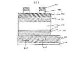
【0068】
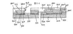
図11は、本発明による代表的な素子の断面構造を表わしたもの、また図12はその平面レイアウトを示したものである。本素子の配線構造およびその製造方法は、通常のLSIと同様のため、図11では、素子基本部分の形成終了時の構造で示し、いわゆる素子間等で行われる配線層については省略している。図11において、250、350はソース、ドレインであり、チャネル150に対して絶縁膜980を介して、ゲート500が電界効果を両側から及ぼしている。ドレイン350とチャネル150間に挟まれた絶縁膜931を通過(トンネル)するキャリアが、ゲート500により制御されている。600はドレイン350から引き出す埋め込み配線層である。
【0069】
この構造では、図2で示したチャネル以外の不要な接合は存在せず、また、チャネルと電極との接合に絶縁膜931を挟むことになり、リーク電流を抑制することができる。
【0070】
以下、図5から図11を用いてその製造工程を説明する。
【0071】
シリコン基板100表面に厚さ500nmの熱酸化膜900を形成する。次いで、この上部にホトレジスト層を形成し、このホトレジスト層を所望形状にパターニングする。そして、こうして準備したシリコン基板を通例の異方性のドライエッチングにより熱酸化膜900中に、例えば300nmの深さの溝102、103を形成する。(図5)
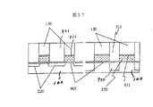
上記基板表面にタングステンを堆積し、CMP(Chemical Mechanical Polishing)法により、溝102、103以外に堆積したタングステンを取り除く。この工程はダマシン法として知られている。これにより、溝102、103中にタングステン600を詰め込んだ構造が得られる。(図6)
上記基板上にチタン100nm(350)、チタンオキサイド5nm(931)を堆積し、さらに、多結晶シリコン200nm(150)を堆積する。この多結晶シリコン層150はチャネルとなる層である。ここを単結晶化することでリーク電流を生じるもととなる粒界の準位を低減することができる。本素子構造は、図5を用いて説明した溝を形成する以外、パターニングを行う工程を有さない。また、溝を用いて形成した下部配線層は、図11に示したように、チャネル部150等の下に配置している。そのため、最初に積層構造をはり合せることで形成し、上部から積層をパターニング加工することで形成することができる。そのため、単結晶を用いたチャネルを実現することができる。(図7)
また、前記のチタンオキサイド堆積後、ニッケル薄膜を堆積する。こののち、アモルファス状のシリコンを堆積し、550℃の低温熱処理を加えることで、ニッケルをシリコン中移動させ、多結晶シリコン層150を結晶化することができる。これにより良好な結晶性を持つチャネル領域を得ることができる。尚、このニッケル薄膜は、2nmより10nmの厚さの範囲、より好ましくは3nmより6nmの範囲で選択される。又、前記の結晶化処理を終えて後、このニッケル層を除去することも出来る。
【0072】
ホトレジストを用いてパターニングを行い、多結晶シリコン、チタンオキサイド、チタンを加工し、溝以外では酸化膜900表面を露出させる。 こうして準備した半導体基体上に、酸化膜920を堆積する。次いで、この表面をCMP法により酸化膜920をエッチングし、この酸化膜920の表面を多結晶シリコン層150表面に合わせて平坦化を行う。次いで、この上部に不純物を高濃度にドーピングした多結晶層250、さらにシリコン窒化膜950を堆積する。このとき、不純物を高濃度にドーピングした多結晶層250の堆積前に多結晶シリコン層150表面を窒化することで、極めて薄い絶縁膜を形成することができる。この薄い絶縁膜によって、多結晶シリコン層150中への、外部からの不純物の拡散を抑えることができる。この絶縁膜は、チャネルの電流駆動力に対しては負荷となるため、必要な熱処理に比べチャネル長を確保できる場合には、多結晶シリコン層150上に直接堆積することができる。尚、ここで、前記チャネル長は多結晶シリコン150の厚さに相当する。
【0073】
電極層250として、Pt、Er等のシリサイドや金属窒化膜、例えばTiNやWN等を耐熱バリア層として堆積したのち、さらに金属材(例えば、タングステン等)の層を積層して形成することができる。該窒化膜および金属層を920表面までエッチングする。断面構造では現れていないが、このとき、図12に符号250で示したようにコンタクト(720)形成の引き出しを形成する。(図8)
こうして準備した基体の上部にシリコン酸化膜921を堆積し、CMP法により表面を平坦化する。ここでは、以下層間膜となる堆積積層された酸化膜層は符号921で示す。(図9)
更に、この基体の上部に、通例のフォトレジストを用いたゲートパターンを形成する。そして、このゲートパターンを用いたエッチング方法によって、層間絶縁膜921に溝104を形成する。電極層250およびチャネルとなる多結晶シリコン150の側面を露出させる。(図10)
前記溝104内の積層体の表面に、CVD法により5nmのシリコン酸化膜980を堆積した後、ゲート500を溝内に形成する。ゲート絶縁膜としては、例えばシリコン窒化膜やチタンオキサイドをも用いることができる。尚、図11ではシリコン酸化膜980は溝104の内面の全面に形成されている。このシリコン酸化膜は、この溝104の全面に必ずしも必要はない。例えば、層間絶縁膜921の側壁等は必ずしも必要はない。しかし、この例では酸化膜はCVD法によって形成されている為、溝104の全面に形成されている。このことは、以下の実施の諸形態においても同様である。(図11)
以下、通常のLSIの製造プロセスと同様に配線を形成する。
【0074】
図12は当該半導体装置の主要部よりの引出し用のコンタクト領域の平面レイアウトを示す図である。符号500の領域がゲートに対応する平面的な領域を示している。図は、埋め込み引き出し層600へのコンタクト710、ゲート500へのコンタクト730、電極250へのコンタクト720の配置例を示している。図11に見られるように、この構造では、電極350はチャネル150との間にバリア931が挟まれているため、リーク電流を強く抑制することができる。
【0075】
また、電極250に高濃度にドーピングした多結晶シリコンを用いた場合、該電極がチャネルのキャリアの供給源となるため、不純物による導電型により、N型およびP型のデバイスを形成することができる。
【0076】
上記の実施例では、引き出し形成のため、上部電極250をチャネルパターニング後形成しているが、チャネル150と同時に形成することができる。この例を、図13から図17を用いて説明する。
【0077】
本例においては、上記実施例の図5より図7までと同様に製造される。即ち、所定の基体に、配線600、及びチタン層350、チタンオキサイド層931、多結晶シリコン層150が形成される。こうして準備された基体の上部に、更に、チタンオキサイド層932、チタン層250、絶縁膜950を堆積する。(図13)
この基体の上部に、通例のフォトレジストを用いたゲートパターンを形成する。そして、このゲートパターンを用いたエッチング方法によって、酸化膜900表面が露出するまで、該積層膜をエッチングする。(図14)
次いで、基体位上に、酸化膜920を堆積した後、CMP法により平坦化し、更に、絶縁膜950表面が露出するまでエッチバックする。(図15)
更に、この基体の上部に、通例のフォトレジストを用いたゲートパターンを形成する。そして、このゲートパターンを用いたエッチング方法によって、層920に溝105を形成する。こうして形成した溝105内の積層体の側壁にゲート絶縁膜980形成する。更に、溝105中にゲート層500を堆積する。そして、ゲート層500をエッチバックすることで、電極層250側面までゲート層500が埋め込む構造とする。(図16) ゲート層500上の溝を絶縁膜921で埋めた後、表面を平坦化し、絶縁膜950を露出させる。そして、絶縁膜950を除去した後、金属材の層650を形成することにより電極層250に対する配線を形成する。この工程は通常のコンタクトホール形成および金属配線形成プロセスと同様である。こうして、ゲート層500および埋め込み層600へのコンタクト形成および配線形成を同時に行うことができる。(図17)
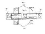
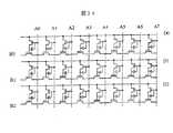
本素子を集積回路に用いた場合の有効性を示すため、代表的演算ゲートであるOR回路とAND回路(あるいはNAND回路)を形成する例を示す。
【0078】
図18は4入力のOR回路を示す等価回路図である。図19はこれに対応した電極部の平面レイアウトを示す図である。尚、図19においては、全体の配置を示すため、ゲート層500、引き出し部600、および電極250引き出しと、それぞれのコンタクトのみを記した。
【0079】
図18に示す回路自体は通例のものであるが、本願発明は、この回路を構成する絶縁ゲート型電界効果型トランジスタのチャネル領域の構造およびその各部の取りだし構造に特徴を有する。図において理解を容易にする為、本願発明に係わる絶縁ゲート型電界効果型トランジスタのチャネル領域は波線で示した。
【0080】
図20は3入力のAND回路の等価回路図である。図21はこれに対応した電極部の平面レイアウトを示す図である。引き出し部600と電極250を、交互につないで行くことで、回路上の素子の縦積みが形成できる。従って、本例は極めて小型化に有利である。図21では、この様子を解りやすくするため、上部引き出し層である電極層250をハッチングで示した。
【0081】
前述したように、本発明の構造を用いて、不純物の選択によりCMOSのような相補型の素子を形成することができる。即ち、本願発明の構造では、電極250形成時に、イオン打ち込み法により、ドーピングする不純物の導電型を変えることができるためである。
【0082】
図22はインバータの例の電極部の平面レイアウトを示す図である。この例は、本願発明の半導体装置の構造を用い、且つそのチャネル領域がN型およびP型の各素子を用いてインバータを形成したものである。2つの電極250のうち、上側には、砒素を、下側にはボロンをドーピングしている。ゲートコンタクト730が入力端子、引き出し600へのコンタクト720が出力端子である。配線650により電極層250へ、それぞれ、グランド電位、電源電位が給電されている。
【0083】
図23は、インバータを2段接続した様子を示す電極部の平面レイアウトを示す図である。即ち、図23の構造は図22の構造を2段接続した構造である。入力730と出力720を重ねることで、2つのインバータの接続がなされている。
【0084】
プロセスにおいては、ゲート500堆積前にコンタクト720を形成することで、直接次段と連結することができる。
【0085】
本願発明の素子構造では、縦形構造を用いているため、上部電極250からの引き出し配線の形成が一つの課題である。上記実施例以外の引き出し形成方法について、図24から図29を用いて説明する。図24から図29は、本例を説明するため、製造工程順に示した素子の断面図である。
【0086】
本願発明の製造方法を説明した工程によって前記図13と同様の積層体を得る。即ち、半導体基板100の上部に、絶縁層900が設けられ、この絶縁膜に埋め込み配線600等を形成される。そして、こうして準備した基体の上部に、金属電極350を構成するチタン層、トンネル絶縁膜931となるチタンオキサイド層、チャネル領域150となる多結晶シリコン層、更に、第2の導電領域250を構成するチタン層、上部の絶縁物層920としてのシリコン酸化物層を積層する。そして、電界効果型トランジスタのキャリアの進行方向、即ち、チャネル方向に所望形状を得る為、通例の方法によって、パターニングを行う。図24は、紙面垂直方向にパターニングされた柱状積層膜(層350、150、250、920)の断面を示したものである。(図24)
こうして準備した基体上に、ゲート絶縁膜を形成後、ゲート電極層500および絶縁膜955を積層する。尚、前記ゲート絶縁膜は層500と層920の間に存在するが、図25ではその断面の取り方で現れていない。又、絶縁膜955はシリコン窒化膜を用いた。そして、これらの積層体、層500,及び層955を所望形状にパターニングを行う。図25では、断面の取り方によって柱上のみゲート断面が示されている。例えば、図16に見られるように、層500は溝105内に深く形成されている。同様の構造は本例でも存在すると言うことである。(図25)
次いで、前記層500及び層955の側壁に、スペーサとなる絶縁膜956を堆積後する。絶縁膜955、絶縁膜956の領域をマスク領域として、積層膜920、250、150、350を、所望形状にエッチングする。尚、絶縁膜955及び956の形成は、例えば、通例のCVD法によれば良い。(図26)
こうして、準備した基体上に、酸化膜921を堆積し、更に、CMP法により、積層体の表面を平坦化する。(図27)
引き出し形成部に対応する領域に開口を有するマスクをかけ、且つ、絶縁膜955、絶縁膜956の領域をマスク領域として溝を形成し、導電体層250側面を露出せしめる。(図28)
この溝の内部にタングステン625を埋め込むことで、引き出し配線を形成する。これにより隣接する素子同士を自己整合的に接続してゆくことができる。即ち、図29における、各導電層250の領域が溝部251によって隔てられているが、タングステン層625によって相互に電気的に接続される。そして、このタングステン層625は、これまでに形成された溝251によってその寸法を規定されている。即ち、本例では、溝形成の為に用いるマスクの形成によって、その後の寸法規定がなされている。(図29)
本願発明の半導体装置は、電極のリークを極めて低く抑えられることに特徴がある。この特徴を活かす上で、一般に、電荷によって情報の記憶を行うメモリ素子への応用が好適である。なかでもゲインセルと呼ばれるタイプに用いることで、優れた半導体記憶装置を供することができる。
【0087】
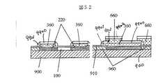
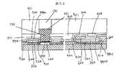
図30は主要部のみを模式的に示したゲインセルでの本願発明に係る半導体装置の適応例の断面図である。メモリセルは、半導体基板100に形成された素子による読み出し部と、本発明素子を用いた記憶情報書き込み部よりなる。
【0088】
半導体基板100に通例の不純物領域220、および320が形成され、電界効果型トランジスタのチャネル領域を構成する。このチャネル領域を覆ってゲート絶縁膜970が形成される。こうして構成されたトランジスタ部が前記の読み出し部となる。そして、この上部に次のような記憶情報書き込み部が形成される。尚、前記記憶情報書き込み部となる半導体装置は、これまで述べてきた本願発明に係る素子であるので、ここではその詳細の説明は省略する。図30において、符号931はトンネル絶縁膜、150はチャネルとなる半導体層、250は第2の導電体層、980はゲート絶縁膜、500はゲート電極層である。
【0089】
電極となる導電領域350は、前記ゲート絶縁膜970の上部に直接形成され、書き込み素子のドレインであるとともに、読み出し素子のゲート電極となっている。本メモリセルにおいては、電極350のもつ電荷により情報として記憶され、その読み出し素子に与える電界効果によって、チャネル特性を変化させ、電極220、320間を流れる電流として、情報が読み出される。記憶保持部である導電領域350のリークが少ないことが、良好な情報保持性能を可能にしている。ここで導電領域350は記憶保持部であるため、抵抗値はあまり重要ではない。そのため、高濃度に不純物をドーピングすることで金属化した多結晶シリコンを用いてこの導電領域、電極層を形成してもよい。
【0090】
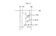
代表的メモリ素子の基本回路構成の例を図31及び図32に示した。次に、これらのメモリセルの動作について説明する。
【0091】
図31は、図30に示した半導体素子を等価的に示したメモリセルの回路図である。回路の理解を容易にする為に、図31の2つのトランジスタT1、T2に対して、図30の構造図に示した各部の符号を付した。素子T1読み出し部を構成するトランジスタ、素子T2は本願発明に係る半導体装置を用いた記憶情報書き込み部である。
【0092】
D1は読み出しワード線、D2は書き込みワード線、D3は書き込みデータ線、D4は読み出しデータ線である。D2をオンさせることで、記憶保持部(ゲート電極)にD3電位を書き込み、オフすることで、電荷を保持させる。このとき、読み出し素子のゲート電位が決められる。例えば、ゲート電位がトランジスタの閾値を超えている場合、D1、D4間に電位差を与えると、電流が流れる。一方、ゲート電位が閾値より低い場合、D1、D4間に電位差を与えても電流は流れない。そのため、この電流によって、ゲート電位を読み出すことができる。
【0093】
図59は上記の例での各信号の例のタイムチャートである。D1、D2、D3、およびD4は各々読み出しワード線、書き込みワード線、書き込みデータ線、読み出しデータ線への電圧の印加を示している。ここでは、図31に示した配線記号を用いている。図59は、同一導電型素子を書き込み、読み出し素子に用いたメモリセルによる書き込み(tw)、読み出し(tr)を繰り返す例を示している。ここでは、読み出し時に、D4の電位変化を読み取り、センスアンプにより駆動させる例を示している。D4はtrステップの前に一度中間電位を与え、そこからの変化で読み出す例を示している。
【0094】
この構造では、書き込み部と読み出し部が、動作上分離されているため、集積化しても、読み出し動作が他のセルの情報を破壊する問題は生じてこない。図31に示した等価回路図では、D1とD2、D3とD4とが各組毎に幾何学的に平行になるように配置されている。しかし、実際の半導体装置の構造では、少なくともD1とD4、D2とD3が幾何学的に直交するように配置されていればよい。D1とD2、D3とD4とは、必ずしも幾何学的に平行に配置する必要はない。それは、読み出しと書き込みが分離されているためである。
【0095】
図32は、書き込みと読み出しのワード線をD4に兼用させたものである。動作を説明するために、容量素子910を積極的に加えている。しかし、実際の構造においては、電極350とゲート500にはオーバーラップが存在するため、特別なプロセスを追加することなく形成することができる。いわゆる寄生容量を設定し、これをもってこの容量となすことが可能である。
【0096】
D1、D3は読み出しデータ線、D2は書き込みデータ線、D4はワード線である。書き込み素子と、読み出し素子を反対導電型によって形成すると、相補的に動作させることができる。例えば、書き込み素子をP型、読み出し素子をN型としたとき、書き込み素子はワード線D4に負電位を加えることでオン状態となり、電位が書き込まれる。一方、読み出し素子においては、正電位を加えることで、チャネルはオン状態となる。すなわち、D4に正電位を加えることで、容量カップリングにより読み出し素子のゲートに正電位を与えることができる。このとき、書き込み素子においては、よりオフ状態が強まるため、電荷リークを抑えることができる。従来のゲインセルでは、相補的動作ができなかったため、書き込み(消去)時に、最も高いゲート電圧を与え、その情報を破壊しないように、それより、低い電圧で読み出す必要があった。そのため、情報として使える電位範囲が狭く、多値情報を持たせることが困難であった。相補的動作においては、読み出し時のワード線電位には、こうした制約がないため、多値の情報(多段階の電位状態)を用いることができる。
【0097】
図60は、相補型メモリセルの基本動作のタイムチャートを示している。ここで、D2が書き込み(tw)時と読み出し(tr)時に反対方向にバイアスされるのが特徴である。図60において、4値の電位を記憶ノードに順次書き込み、それぞれ読み出し動作を繰り返す例を示している。ここで、D4ha電流センスを与え、一定電位で動作させる例を示している。尚、D1、D3は読み出しデータ線、D2は書き込みデータ線、D4はワード線に対する電圧を示している。D3の電圧状態に見られるように、例えば実質的に4値の情報を用いることが可能となる。
【0098】
また、読み出し時のゲート電位にデータ破壊による制約がないことから、自由に印加電位を与えることができるため、デジタル化したものではなく、保持電荷状態を連続した状態として読み出すこともできる。また、ゲート印加電圧と保持電荷状態により読み出し結果が与えられることから、これを用いて演算処理を行うことができる。
【0099】
図33は図31のメモリセルのアレイ状に配置した例を示したものである。C0は書き込みワード線のドライバ部、C1は書き込みデータ線のドライバ部、C2は読み出しワード線のドライバ部、C3は読み出しデータ線のセンス部である。図33で各メモリセル部は前述したところであるので、ここでは詳細は省略する。本例は通例のメモリ装置の駆動方法を取ることが出来る。
【0100】
本願発明の半導体装置の構造におけるリーク電流の抑制は、電極とチャネル部に挟まれた絶縁膜のトンネル現象をゲート電極により有効に制御することで成り立っている。すなわち、書き込み素子ゲートと記憶保持部であるドレイン電極の電位関係を保持することが、リーク電流低減において重要である。そこで、本メモリ素子応用において、書き込みワード線をある電位状態で安定化することができる装置Rをおくことが有効である。この手段については、前述した通り、例えば装置Rとして抵抗を接続することで十分である。この手段Rによって、書き込みワード線の電位を通常、接地電位となるようにすることができる。
【0101】
すなわち、この記憶装置が電源から切り離されても、ワード線は接地電位に固定されリーク電流は抑制できるため、長時間、情報を保持し続けることができる。装置Rとして抵抗を用いた場合、動作状態、すなわちワード線が選択された状態では、消費電力を増大させることになるが、選択されるワード線は最大でもアレイ中一本であり、適当な大きさの抵抗を選ぶことでそれほど消費電力を増大させることなく良好な情報保持特性を得ることができる。
【0102】
図32に示したメモリセルを用いても、図33と同様にメモリセルアレイを形成することができる。他方、図34に示すように多段のメモリセルを積み重ねる、いわゆるNAND型のアレイを組むことが有効である。相補的に働かせることができるため、同一の読み出しデータ線であるB0、B1、B2に連なるセルを、A0からA7に順次電圧を加えることでオンさせることができるためである。そのため、データ線が、拡散層とチャネルによって形成されるため、配線およびコンタクトの形成を減らすことができる。そのためメモリセルの微細化が容易になり、高集積化することが可能になる。
【0103】
図35から図40を用いて、代表的メモリセルの形成プロセスを説明する。これらの図は、半導体記憶装置の断面構造を示している。また、図には、中央のギャップを挟んで左右でそれぞれ別の断面での様子を示している。図の左側の断面図ではゲート電極500が紙面に垂直に延在するような断面、右側の断面図では紙面の面内にゲート電極500を含む断面である。
【0104】
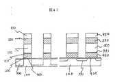
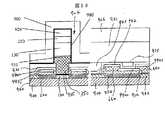
シリコン基板100上に通常のMOSLSIの形成に用いられる浅溝素子分離法により、素子分離絶縁膜900を形成する。次に、露出したシリコン表面を熱酸化することで、読み出し素子用ゲート絶縁膜905を形成する。その上に、記憶ノードとなる金属電極350およびトンネル膜931、チャネル150を積層する。(図35)
チャネル領域となる半導体層150および電極350を、通例のホトレジスト法により所望形状にパターニングする。こうして溝105が形成される。次いで、前記の加工によって開口された領域にイオン打ち込みを行い拡散層220を形成する。(図36)
こうして準備した基板上に酸化膜921を堆積し、その表面をCMP法により平坦化し、多結晶シリコン150が露出するまでエッチバックする。(図37)不純物拡散抑制のために薄い窒化膜を形成したのち、高濃度不純物をドーピングした多結晶シリコン250を堆積する。そして、この多結晶シリコン250を所望形状に加工し、書き込み素子データ線250とする。尚、ここで、前記不純物拡散抑制のために薄い窒化膜は図示が省略されている。(図38)
書き込み素子用ゲート形成部の酸化膜をエッチングし溝107を形成する。こうして、露出したチャネル領域150の少なくとも側面等にゲート絶縁膜980を堆積する。拡散層上に形成した絶縁膜は、耐圧劣化が大きいことが知られている。そのため、ここでは、スペーサとなる絶縁層935をおいて耐圧向上を図っている。スペーサおよび拡散層を除き、基板上にゲート絶縁膜を形成することで、拡散層の代わりにゲートの電界効果による反転層によりソース、ドレインを形成してもよい。(図39)
ゲート層500を形成し、次いで、この層500を書き込み素子ワード線としてパターニングする。図40の右側の断面図では所望形状とされたゲート500が、左側の断面図では溝部107に存在するゲート電極がしめされている。本メモリセルは、シリコン基板上に形成されているので、従来のMOSFETと整合性よく集積することができる。(図40)
次に、上記とは異なる別なメモリセル形成法を、図41から図46を用いて説明する。これらの図においては、前記と同じく、2つの断面構造を合わせてしめしている。
【0105】
素子分離領域900を形成したシリコン基板100上に、読み出し素子のゲート絶縁膜905、記憶ノードとなる電極250、トンネル膜931、チャネル150、上部電極250、電極保護膜950を積層する。(図41)
読み出しデータ方向に溝状201に積層膜を加工し、イオン打ち込み法により、電極220を形成する。(図42)
データ線と直交するワード線方向にワード線パターンにより積層膜を加工する。(図43)
ゲート絶縁膜980形成後、ゲート500を堆積しエッチングすることで、柱状積層膜周囲にスペーサ状のゲートを形成する。この時、図中右に示したようにワード線方向の柱間隔を、データ線方向(図中左)に比べ狭くし、かつ、500の堆積厚さをワード線方向間隔の1/2以上、データ線方向間隔の1/2以下とすることで、ワード線方向のみ、自己整合的にゲート電極を接続することができる。(図44)
こうして準備した基体の上部に、層間膜921を堆積、そして、これを平坦化し電極保護膜950を露出させる。(図45)
電極保護膜950を除去し、金属配線625を堆積する。そして、この金属配線625を所望形状に加工することで、書き込み素子データ線を形成することができる。(図46)
尚、本メモリセルにおいて、ゲート500形成前(図41の段階後)一旦酸化膜で平坦化しエッチバックすることで、シールド層935を形成することができる。(図47)これにより、書き込み素子と読み出し素子の相互干渉を減らし、また読み出し素子の耐圧を向上することができる。
【0106】
更に、その他のメモリセル形成方法を、図48から図58を用いて説明する。図48は図31に示したメモリセルをアレー状に配置した半導体記憶装置のレイアウトである。ここでは、12セルを用いて示している。図48でのD1、D2、D3、及びD4は各々図31におけるそれに対応する。即ち、D1は読み出しワード線、D2は書き込みワード線、D3は書き込みデータ線、D4は読み出しデータ線を表している。図は各データ線及び各ワード線、コンタクトホール、基体での不純物拡散領域が模式的に示されている。細い線で表された読み出しワード線D1及び読み出しデータ線D4は、半導体積層体での下層に、太い線で表された書き込みワード線D2は上層に配置されている。ハッチングを施された領域は不純物拡散領域である。又、細い線で示されたコンタクトホール1003は下層に配置されたD3とD4、あるいはD3とD1とを接続する為の開口部である。一方、太い線で表されたコンタクトホール1002はD3と上層に配置された書き込みワード線D2とを接続する為の開口部である。より具体的には以下の図49から図58の断面図によって明らかにされる。
【0107】
また、図49から図58は図48のA−A、B−B断面を、それぞれ左、右に分けて同時に示したものである。
【0108】
図49より図58までは、SOI(Silicon On Insulator)基板を用いてメモリセルを形成する方法を示す。勿論、前記メモリセルにおいても、読み出し素子をSOI基板に形成できることは明白である。
【0109】
先ず、支持基板1200に搭載された埋め込み酸化膜900上にシリコン層(SOI)100、および、保護層910としての酸化膜を持ったウエハを準備する。支持基板1200は通例シリコンである。支持基板は構造、動作の基本に直接関係ないので、以下の図面ではこの支持基板は図示を省略する。(図49)
前記のウエハに、通例の浅溝分離法により素子分離領域960および保護膜910を再び形成する。また熱処理を加えることで、必要な拡散層220を形成する。(図50)
保護膜910にコンタクト形成部に対応した開口901する。そして、この開口部901を通して高濃度ドープした多結晶シリコン360を堆積し、読み出しワード線および引き出し層を形成する。そして、この上部に絶縁膜9900および9901を形成し、これらを所望形状にパターニングする。(図51)
こうして準備した半導体基体の引き出し層上部にコンタクトを開口902する。そして、再び、この上部に高濃度ドープした多結晶シリコン膜660、及び層間絶縁膜9902を堆積する。そして、層間絶縁膜9902を通例の方法で所望形状になし、この層間絶縁膜9902をマスク領域として、前記多結晶シリコン膜660を読み出しデータ線の所望形状に形成する。(図52)
次いで、層間絶縁膜922および層間絶縁膜層923を堆積した後、表面をCMP法により平坦化する。ここで、絶縁膜922は例えばシリコン窒化膜、絶縁膜923は例えばシリコン酸化膜である。(図53)
次いで、書き込み素子形成部の層間膜を除去し開口903を形成する。この開口内にシリコン100の表面が露出する。(図54)
更に、ゲート酸化膜905形成後、メタル電極350、トンネル膜931、多結晶シリコン150を積層する。(図55)
この積層膜、350、931、150を食刻し、絶縁膜923の表面まで柱状に加工する。この上部に層間絶縁膜921を堆積し、エッチバックすることで、多結晶シリコン膜150を露出せしめる。(図56)
前記多結晶シリコン膜150上に、書き込みデータ線250を形成する。更に、この書き込みデータ線250を覆って層間絶縁膜926を形成し、この層により、積層体の表面を平坦化する。(図57)
層間絶縁膜926、921にゲートパターンに応ずる溝904を形成する。少なくとも露出した半導体層150の側壁にゲート絶縁膜980を形成する。そして、このゲート絶縁膜980を覆って書き込みワード線500を形成する。この構造では、ゲート電極と前記書き込みワード線が同一の層で形成されてれいる。(図58)
上述したこれらの方法により、すぐれた書き込み、記憶保持性能を有する半導体記憶装置を形成することができる。
【0110】
電界効果型トランジスタにおいて、ショットキー接合に絶縁膜を挟み、トンネル現象を制御することで、ソース、ドレインとなる電極のリーク電流を極めて低く抑制することができた。また、この低リーク特性を応用することで、優れた情報保持特性をもった半導体記憶装置を形成することができる。
【0111】
以上、本願発明によれば、リーク電流の極めて低い電界効果型トランジスタを提供することが出来る。
【0112】
本願発明の別な形態によれば、優れた情報保持特性をもった半導体記憶装置を提供することが出来る。
【0113】
本願発明の製造方法によれば、新規な装置をリーク電流の極めて低い電界効果型トランジスタ、あるいは半導体記憶装置を簡便に製造することが出来る。
【0114】
【発明の効果】
本願発明によれば、リーク電流の極めて低い電界効果型トランジスタを提供することが出来る。
【0115】
本願発明の別な形態によれば、優れた情報保持特性をもった半導体記憶装置を提供することが出来る。
【0116】
本願発明の製造方法によれば、新規な装置をリーク電流の極めて低い電界効果型トランジスタ、あるいは半導体記憶装置を簡便に製造することが出来る。
【図面の簡単な説明】
【図1】図1は従来の素子構造を表わした代表的素子断面図である。
【図2】図2はその他の従来の素子構造を模式的に示した断面構造図である。
【図3】図3は従来のショットキー接合を説明するバンド図である。
【図4】図4は本発明で用いる接合を説明するバンド図である。
【図5】図5は素子製造工程を説明する断面構造図である。
【図6】図6は素子製造工程を説明する断面構造図である。
【図7】図7は素子製造工程を説明する断面構造図である。
【図8】図8は素子製造工程を説明する断面構造図である。
【図9】図9は素子製造工程を説明する断面構造図である。
【図10】図10は素子製造工程を説明する断面構造図である。
【図11】図11は素子製造工程を説明する断面構造図である。
【図12】図12は素子平面配置を説明する平面レイアウト図である。
【図13】図13はその他の形態の素子製造工程を説明する断面構造図である。
【図14】図14はその他の形態の素子製造工程を説明する断面構造図である。
【図15】図15はその他の形態の素子製造工程を説明する断面構造図である。
【図16】図16はその他の形態の素子製造工程を説明する断面構造図である。
【図17】図17はその他の形態の素子製造工程を説明する断面構造図である。
【図18】図18はORゲートを説明する等価回路図である。
【図19】図19はORゲートの平面配置を説明する平面レイアウト図である。
【図20】図20はANDゲートを説明する等価回路図である。
【図21】図21はANDゲートの平面配置を説明する平面レイアウト図である。
【図22】図22はインバータゲートの平面配置を説明する平面レイアウト図である。
【図23】図23は多段インバータゲートの平面配置を説明する平面レイアウト図である。
【図24】図24はその他の素子製造工程を説明する断面構造図である。
【図25】図25はその他の素子製造工程を説明する断面構造図である。
【図26】図26はその他の素子製造工程を説明する断面構造図である。
【図27】図27はその他の素子製造工程を説明する断面構造図である。
【図28】図28はその他の素子製造工程を説明する断面構造図である。
【図29】図29はその他の素子製造工程を説明する断面構造図である。
【図30】図30はメモリセル素子構造を模式的に示した断面構造図である。
【図31】図31はメモリセルを説明する等価回路図である。
【図32】図32はその他のメモリセルを説明する等価回路図である。
【図33】図33はメモリセルアレイを説明する等価回路図である。
【図34】図34はメモリセルアレイを説明する等価回路図である。
【図35】図35はメモリセルの素子製造工程を説明する断面構造図である。
【図36】図36はメモリセルの素子製造工程を説明する断面構造図である。
【図37】図37はメモリセルの素子製造工程を説明する断面構造図である。
【図38】図38はメモリセルの素子製造工程を説明する断面構造図である。
【図39】図39はメモリセルの素子製造工程を説明する断面構造図である。
【図40】図40はメモリセルの素子製造工程を説明する断面構造図である。
【図41】図41はその他のメモリセルの素子製造工程を説明する断面構造図である。
【図42】図42はその他のメモリセルの素子製造工程を説明する断面構造図である。
【図43】図43はその他のメモリセルの素子製造工程を説明する断面構造図である。
【図44】図44はその他のメモリセルの素子製造工程を説明する断面構造図である。
【図45】図45はその他のメモリセルの素子製造工程を説明する断面構造図である。
【図46】図46はその他のメモリセルの素子製造工程を説明する断面構造図である。
【図47】図47はその他のメモリセルの素子製造工程を説明する断面構造図である。
【図48】図48はメモリセルアレイの平面配置を説明する平面レイアウト図である。
【図49】図49は多段インバータゲートの平面配置を説明する平面レイアウト図である。
【図50】図50は多段インバータゲートの平面配置を説明する平面レイアウト図である。
【図51】図51は多段インバータゲートの平面配置を説明する平面レイアウト図である。
【図52】図52は多段インバータゲートの平面配置を説明する平面レイアウト図である。
【図53】図53は多段インバータゲートの平面配置を説明する平面レイアウト図である。
【図54】図54は多段インバータゲートの平面配置を説明する平面レイアウト図である。
【図55】図55は多段インバータゲートの平面配置を説明する平面レイアウト図である。
【図56】図56は多段インバータゲートの平面配置を説明する平面レイアウト図である。
【図57】図57は多段インバータゲートの平面配置を説明する平面レイアウト図である。
【図58】図58は多段インバータゲートの平面配置を説明する平面レイアウト図である。
【図59】図59は半導体メモリの基本動作に対するタイムチャートを示す図である。
【図60】図60は多値情報を取り扱う半導体記憶装置の基本動作に対するタイムチャートを示す図である。
【符号の説明】
100、110:シリコン基板、150:多結晶シリコン、320:不純物拡散層電極、500、510:ゲート電極、250、350:電極、600、625、660:金属配線、710、720、730:コンタクト、900、901、905、910、920、921、922、923、924、925、926、931、932、955、956、960、980:絶縁膜層。[0001]
BACKGROUND OF THE INVENTION
The present invention relates to a semiconductor device capable of large-scale integration, and a semiconductor memory device using the same. Furthermore, the present invention relates to a method for manufacturing this semiconductor device or semiconductor memory device.
[0002]
[Prior art]
The main part of a ULSI transistor using a silicon substrate, which is a typical integrated semiconductor device at present, has a cross-sectional structure as shown in FIG. The transistor used in the CMOS is formed using an insulated gate transistor in which a diffusion layer (200, 300) doped with a high concentration of impurities as a source and a drain is used as an electrode region on a
[0003]
In an insulated gate transistor and a MOSFET as a representative example, the carrier of the channel to be controlled uses only the conduction type carrier opposite to the substrate serving as the channel. Therefore, the insulated gate transistor is called a unipolar device. In a unipolar device, it is fundamental in device operation that electrodes such as a source and a drain are electrically separated from the
[0004]
Further, as a different approach, it is considered that the diffusion layer electrode is surrounded by an insulating film layer and a barrier against leakage is provided between the electrode and the channel (substrate). Further, the structure found in Japanese Patent Application Laid-Open No. 10-200001 is a structure in which a multilayer insulating film layer is sandwiched not only between the diffusion layer electrode and the channel but also in the channel portion. However, the latter can be regarded as a kind of structure called a thin film transistor (TFT) in which the channel portion is formed of a polycrystal instead of a single crystal in the manufacturing process. In these structures, it is possible to suppress leakage without increasing the diffusion layer resistance. However, since it is necessary to flow a channel current through the insulating film, there is a problem that the current driving force is reduced. come.
[0005]
As a method for solving the increase in electrode resistance due to the shallow junction, it has been proposed to use a metal material for the source and drain. In general, the electrode and the substrate are separated from each other not by a PN junction but by a Schottky junction formed at a contact portion between a metal and a semiconductor. Therefore, this is called a Schottky barrier source / drain MOSFET (SB-MOSFET). . These structures have been studied, for example, by Tucker et al. In Applied, Physics, Letter, Vol. 65, pages 618 to 620 (Appl. Phys. Lett. 65 (5), pp. 618-620, 1994). Yes. As an actual prototype, S, P, I, E, Conference, ON, Microelectronic, Device, Technology, Two, July 1998, S, P, I, E, 3506, pages 230 to 233 (Part of the SPIE Conference on Microelectronic Device Technology II, SPIE vol. 3506, pp.230-233) reports Wang et al. In these reports, it has become clear that, as an effect of using a Schottky junction, leakage between junctions can be effectively suppressed even in a short channel structure in which the distance between the source and the drain is reduced. However, since it is difficult to form a good junction as compared to the PN junction, the leakage between the substrate and the substrate increases, canceling the effect of reducing the leakage between the source and drain, and reducing the on-resistance of the junction. Since it is high, the effect of reducing electrode resistance is not visible.
[0006]
Further, as gain cells used in semiconductor memory devices, for example, p-type MOS for writing and n-type MOS for reading can be seen in IEDM 92 and 1006-1008 by Shoji Shukuri et al.
[0007]
[Problems to be solved by the invention]
The first object of the present application is to provide an insulated gate field effect transistor with extremely low leakage current. In other words, the present invention suppresses a decrease in driving force caused by the above-described various measures that have been taken to reduce the leakage current that has been increased to reduce the channel length.
[0008]
The second object of the present application is to provide a semiconductor memory device having good memory characteristics. Using the insulated gate field effect transistor having a low leakage current, a three-terminal switching element with a low leakage current can be obtained. Therefore, this is particularly effective in forming a semiconductor memory element.
[0009]
Still another object of the present application is to provide a manufacturing method for providing the semiconductor device or the semiconductor memory device.
[0010]
[Means for Solving the Problems]
First, in order to facilitate the understanding of the invention, the gist of the inventive idea of the present invention will be described. Further, various embodiments of the invention will be described in the section of the embodiment of the invention.
[0011]
In the Schottky junction, since the interface of different materials is formed between the junctions, the junction leakage is larger than that of the PN junction. When the SB-MOSFET is formed based on the conventional structure shown in FIG. 1, only the gate end junction is used for switching, and the bottom surface is unnecessary for the switching operation. This bottom surface is the main source of leakage because it occupies most of the area of the junction. In order to suppress such unnecessary leakage, as schematically shown in FIG. 2, it is effective to use a structure in which the channel 101 is sandwiched from both sides by the
[0012]
In order to further suppress leakage, an insulating layer serving as a barrier that prevents leakage is sandwiched between a metal and a semiconductor. This applies a structure in which the periphery of the diffusion layer electrode is surrounded by an insulating film.
[0013]
FIG. 3 is a band structure diagram for explaining a typical Shottky junction. FIG. 3 shows the junction region between the
[0014]
That is, in the Schottky junction, as shown in the band diagram of FIG. 3, the leakage current is suppressed by a barrier Pm called a Schottky barrier. As shown in FIG. 4, carriers passing from the metal side to the semiconductor side can be reduced by sandwiching an insulating film having a larger barrier height Pi than Pm. A junction having an insulating layer in place of the Schottky junction is known as a MIS junction (Metal Insulation Junction). Examples of this are described, for example, on pages 540-553 of Physics of Semiconductor Devices, second edition, JOHN WILEY & SONS by Sze. Even when an insulating layer having such a high barrier height Pi is interposed, the tunneling phenomenon can be promoted by making the thickness of the insulating layer extremely thin, so that the switching operation of the junction can be performed.
[0015]
In general, carriers passing through the insulating film due to a tunnel phenomenon depend on the barrier height, film thickness, and carrier energy. As the device structure, the barrier height between the metal material and the insulating film, the film thickness of the insulating film, and the potential distribution in the non-equilibrium state can be controlled.
[0016]
In the structure of the present invention, a device having a large channel length is formed without increasing the plane area by adopting a vertical channel arrangement. As a result, an increase in leakage current due to a short channel can be suppressed. Furthermore, by arranging the gates on both sides, the field effect can be utilized more effectively. By adopting this vertical structure, it is possible to easily form an asymmetric transistor which has been difficult in the prior art. Therefore, the barrier made of the insulating film can be formed only on one side, and the decrease in driving force can be suppressed.
[0017]
By effectively extracting these effects, a three-terminal transistor structure that can suppress the leakage current to an extremely low level can be obtained. Further, it will be described based on an embodiment that this low leak characteristic is effective in forming a semiconductor memory device excellent in memory holding, writing and reading operations.
[0018]
DETAILED DESCRIPTION OF THE INVENTION
Prior to specific description of the embodiments of the present invention, outlines of main aspects of the present invention will be listed and described.
[0019]
Semiconductor device according to the present application
A typical first embodiment of the semiconductor device according to the present invention includes a semiconductor region having a first conductive region, a first insulating film, a first semiconductor region, and a second conductive region, and at least the first region. A semiconductor device having a second insulating film provided in the semiconductor region and a third conductive region provided on the film surface of the second insulating film.
[0020]
The present invention can provide a novel switch element. As will be described later, it is extremely useful as a switch section of a novel semiconductor memory device. Further, the structure of the present invention can be manufactured by a usual manufacturing method in the semiconductor field. Therefore, the semiconductor device of the present invention can be provided at a very low cost.
[0021]
A typical second embodiment of the semiconductor device of the present invention includes a semiconductor stacked region in which a first conductive region, a first insulating film, a first semiconductor region, and a second conductive region are stacked, and at least A second insulating film provided on a side surface of the first semiconductor region intersecting with a stacking direction of the semiconductor stacked region, and a third conductive region provided on a film surface of the second insulating film. It is a semiconductor device having.
[0022]
In the above embodiments, the semiconductor region having the first conductive region, the first insulating film, the first semiconductor region, and the second conductive region is used as the charge transfer means and the charge of the insulated gate field effect transistor. Configure the transfer area. The first semiconductor region corresponds to a so-called channel region, and the first and second conductive regions correspond to either a source or a drain. Whether these are referred to as source or drain is only a difference depending on the operating state. Then, the semiconductor region of the first conductive region, the first insulating film, and the first semiconductor region is a stacked body having the band structure described with reference to FIG. In this embodiment, it is an important point that the first insulating film is provided.
[0023]
This first insulating film is typically a metal oxide used as a first conductive region, a low-oxidation oxide, a nitride, a low-nitride nitride, a silicon-metal oxide, or a silicon-metal nitride. Or an insulator including at least two of them is used. More specifically, refractory metals and their oxides, nitrides, or silicides are suitable if examples of these metals and insulators suitable for these metals are used. Furthermore, specific examples may include titanium, titanium silicide, tungsten, tungsten silicide, cobalt, cobalt silicide, platinum, platinum silicide, nickel, nickel silicide, etc. as the metal or metal equivalent conductor. I can do it. As specific examples of the insulator, silicon oxide, silicon nitride, and the like are typical examples. Further, examples of the insulator include oxides or nitrides of the above various metals or refractory metals. Titanium and titanium silicide are thermally stable and are preferable examples. Silicon oxide, silicide, or the like is a material often used in the manufacturing process in the usual semiconductor field, and is convenient for manufacturing the semiconductor device and the semiconductor memory device of the present invention. Of course, according to the request | requirement, the said illustrated metal and an insulator can be used in combination as appropriate.
[0024]
These insulating films have a thickness that exhibits a tunnel effect at the junction. In the case of the thickness of this insulating film, in the case of silicon oxide, 3 nm or less, preferably 1 nm to 2 nm is frequently used.
[0025]
Although specific examples of the first conductive region and the first insulating film have been mentioned, these examples can be applied to various embodiments and embodiments of the invention described in the present specification. It goes without saying that it is a thing.
[0026]
A third form is an insulated gate field effect transistor having a source, a drain, a gate electrode, and a channel region, and has a first insulator layer on a first conductive region that becomes a source or drain electrode. A semiconductor material layer serving as a channel region on the insulating film, a second conductive region serving as a drain or source electrode on the semiconductor layer, and a second insulating film layer disposed on a side surface of the channel region. It can be said that the semiconductor device has a gate electrode that exerts a field effect on the channel region through the second insulating film layer.
[0027]
The following various forms can be considered depending on the selection of the material of each part described above.
[0028]
In the fourth form of the present application, the first conductive region in the above-described forms is formed of a metal material.
[0029]
Furthermore, in the fifth embodiment of the present application, the first conductive region in the above embodiments is formed of a semiconductor material substantially metallized by doping impurities at a high concentration.
[0030]
Furthermore, in the sixth embodiment of the present application, the second conductive region is formed of a semiconductor material substantially metallized by doping impurities at a high concentration.
[0031]
In the present invention, the above conductive regions can be used in combination. That is, in the seventh embodiment of the present application, the first conductive region is formed of a metal material or a semiconductor material metallized by doping an impurity at a high concentration, and the second conductive region is an impurity at a high concentration. It is formed of a semiconductor material metallized by doping.
[0032]
In an eighth aspect of the present application, the first conductive region is formed of a semiconductor material metallized by doping impurities at a high concentration, and the second conductive region is doped with metal materials or impurities at a high concentration. By doing so, it is formed of a metallized semiconductor material.
[0033]
The doping amount of impurities necessary for metallization using the semiconductor material as a base material is sufficient using a range in the usual semiconductor field. The doping amount for silicon is typically 1020cm-ThreeThe range is more than about.
[0034]
It goes without saying that these examples relating to the doping amount can also be applied to the embodiments and embodiments of the invention described in this specification.
[0035]
In the semiconductor device of the present invention, the semiconductor region sandwiched between the first conductive region and the second conductive region constitutes a charge transfer region of the field effect transistor, that is, a so-called channel region. Therefore, in this sense, in the present invention, the charge transfer region is constituted by both the semiconductor region and the tunnel insulating film. Therefore, the example of the form showing this intention can be said as follows.
[0036]
According to a ninth aspect of the present invention, there is provided a semiconductor region having a first conductive region, a first insulating film, a first semiconductor region, and a second conductive region, and the semiconductor region of the second semiconductor region. And a third conductive region provided on the film surface of the second insulating film, and the first or second insulating film. One of the conductive regions is formed of polycrystalline silicon doped with impurities at a high concentration, and the other of the first or second conductive regions is formed of metal, and the first conductive region In the semiconductor device, silicon and a tunnel insulating film are arranged in a current path flowing from the first to the second conductive region.
[0037]
In more detail, the present embodiment shows that the source is formed of polycrystalline silicon doped with high-concentration impurities, the drain is formed of metal, and silicon and a tunnel insulating film in a current path flowing from the source to the drain. It can be said that the semiconductor device is arranged.
[0038]
If the further practical form of the semiconductor device of the embodiments of the present invention described so far is shown, it is said that the semiconductor device is a semiconductor device in which the carrier of the channel portion is depleted when the switching of the semiconductor device is off. I can do it. Semiconductor memory device
Next, the semiconductor device described so far, that is, a semiconductor memory device using an insulated gate field effect transistor will be described.
[0039]
A representative tenth form of the semiconductor memory device is that any one of the semiconductor devices of the present invention described above is an information writing device, the first conductive region is a charge holding portion, and the charge holding portion is electrically connected. A semiconductor memory device having an information reading element connected to the.
[0040]
In the semiconductor memory device, the information reading element is a field effect transistor.
[0041]
In the semiconductor memory device of this embodiment, it is more preferable that the charge holding unit is surrounded by an insulating film and information is stored by the amount of charge held in the charge holding unit.
[0042]
As described above, when a semiconductor memory device is configured by using various embodiments of the semiconductor device according to the present invention as information writing means, the tunnel insulating film of the semiconductor device according to the present invention is formed on the charge storage node side of the semiconductor memory device. It is preferable to connect the conductive regions provided in contact with each other. This is because it is more convenient to secure the accumulated charge. Of course, it goes without saying that the semiconductor memory device can be provided regardless of which of the first and second conductive regions of the semiconductor device is provided on the charge storage node side of the semiconductor memory device.
[0043]
In the case where a semiconductor memory device is configured by using various embodiments of the semiconductor device of the present invention as information writing means, an N-type insulated gate field effect transistor is arranged as a lateral element, and a P-type insulated gate electric field is formed. As an effect transistor, it is more convenient to use it as a vertical element using the tunnel insulating film according to the present application.
[0044]
A typical eleventh aspect of the semiconductor memory device of the present invention is a first path for moving carriers, a means for accumulating charges for generating an electric field that changes the conductivity of the first path, Means for supplying a desired charge to the means for accumulating the charge for a desired voltage, and means for supplying the desired charge to the means for accumulating the charge comprises a metallic electrode. And a junction having a tunnel insulating film and a semiconductor region.
[0045]
In other words, this embodiment is a semiconductor memory device having a source or drain electrode of a field effect transistor (T1) as a semiconductor device according to the present invention and an insulated gate field effect transistor (T2) formed on a semiconductor substrate. The semiconductor memory device is connected to the gate electrode of T2 through the channel of T1. Then, the switching operation is performed using the tunnel insulating film. The field effect transistor (T1) as the semiconductor device according to the present invention has a stacked structure of at least a conductive region-channel region-tunnel insulating film-metal conductive region. Here, the conductive region or the metal conductive region corresponds to the source or drain of the field effect transistor. Therefore, the connection between T1 and T2 has the following form.
[0046]
(1) Conductive region-semiconductor region-tunnel insulating film-metal conductive region-gate of T2,
(2) Metal conductive region-tunnel insulating film-semiconductor region-conductive region-gate of T2
In this case, in the actual structure, the gate of the metal conductive region-T2 in (1) or the gate of the conductive region-T2 in (2) is formed in the same layer and serves as both of them. But more practical.
[0047]
To summarize the operation of the semiconductor memory device of the present invention, in the semiconductor memory device in which information is stored by the charge according to the eleventh embodiment, the charge is taken in and out through the write element T1, and the charge holding state of T2 is determined. It can be said that the reading element is a reading element.
[0048]
According to a twelfth aspect of the semiconductor device of the present invention, there is provided a semiconductor substrate, a first impurity region and a second impurity region provided opposite to the semiconductor substrate, and at least the first impurity region and the second impurity region. A first insulating film covering the first semiconductor region sandwiched between the impurity regions; a first conductive region provided on the first insulating film; a second insulating film; a second semiconductor region; And a semiconductor region having a second conductive region, a third insulating film provided on a side surface of the second semiconductor region intersecting with the stacking direction of the semiconductor region, and a film surface of the third insulating film And a third conductive region provided in the semiconductor device.
[0049]
In this embodiment, the field effect transistor portion constituting the switch element portion is configured in a direction in which the channel region intersects or is substantially orthogonal to the substrate of the semiconductor memory device. This is a so-called vertical semiconductor device. Therefore, this form is advantageous for downsizing of the apparatus. Furthermore, if a structure in which the sidewall of the second semiconductor region is covered with an insulating film is employed, a semiconductor memory device with less leakage current can be provided.
[0050]
Other main forms of the present invention
A thirteenth mode of the present application is the integrated semiconductor device according to the tenth semiconductor device, comprising means for stabilizing the potential between the gate electrode wiring of the writing element and the substrate potential. More specifically, the relative potential relationship between the gate electrode and the conductive region is fixed even when the power is turned off. The simplest and practical means for stabilizing this potential is a resistor. However, many circuits can be used to answer this requirement.
[0051]
In a fourteenth aspect of the present application, for example, in an integrated semiconductor device using at least two of the eleventh or twelfth semiconductor memory devices, a semiconductor in which read elements T2 are arranged in an electrically stacked manner is used. Device.
[0052]
According to a fifteenth aspect of the present application, for example, in the semiconductor memory devices described above, the source and drain potentials of T2 can be changed without changing the gate electrode potential of the write element T1 when information is read. A semiconductor memory device that performs a read operation by applying a potential difference change between the source and drain electrodes.
[0053]
As described above, since the gate potential needs to be fixed, in the semiconductor memory device of the present invention, it is preferable to fix the gate potential and change the source or drain potential.
[0054]
In the sixteenth aspect of the present application, for example, in the semiconductor memory devices described above, when reading information, the gate electrode and the source are changed by changing the source and drain potentials without changing the gate electrode potential of the read element T2. A semiconductor memory device that performs a read operation by applying a potential difference change between drain electrodes.
[0055]
The seventeenth aspect of the present application is, for example, a wiring layer that is arranged in an array using a plurality of the eleventh to twelfth semiconductor memory devices and is connected to the source and drain electrodes of the read element T2 formed on the substrate. Is a semiconductor memory device that is arranged in a plane so as to be orthogonal to each other.
[0056]
According to an eighteenth aspect of the present invention, a semiconductor device or a semiconductor memory device according to the present application, for example, the first, second, tenth, or eleventh semiconductor device or the semiconductor memory device is an SOI (Silicon On Insulator) substrate. This is an integrated semiconductor device formed on top. Since an insulating substrate is used as the substrate, the demand for a semiconductor device or a semiconductor memory device with reduced leakage current according to the present invention functions more effectively.
[0057]
A nineteenth aspect of the present application is an integrated semiconductor device having a device that stabilizes a potential without consuming power between a gate electrode wiring of a writing element and a substrate potential in the integrated semiconductor memory device.
[0058]
A twentieth aspect of the present application is a semiconductor memory device having a writing device using a field effect transistor and a reading device using a field effect transistor having a conductivity type different from that of the writing device.
[0059]
The twenty-first mode of the present application is the semiconductor memory device according to the twenty semiconductor memory device, for example, in which a potential for turning off the channel of the writing element is more applied to the gate electrode of the writing element when reading information than when holding the charge. .
[0060]
A twenty-second form of the present application is an integrated semiconductor device in which, for example, in the twenty semiconductor memory device, potential information to be written has at least three or more values.
[0061]
A twenty-third form of the present application is an integrated semiconductor device that reads out stored charge information as a continuous potential in the semiconductor memory device of 21, for example. A twenty-fourth aspect of the present invention is a semiconductor device to which, for example, in the above-described semiconductor device of 12 or 20, a function for performing arithmetic processing by holding charge and gate electrode potential is added.
[0062]
Main modes of the invention relating to the manufacturing method of the present application
A first embodiment related to the manufacturing method of the present application is a process for forming a first insulating film on a semiconductor substrate, and a semiconductor material metallized by doping a metal layer or impurities at a high concentration on the insulating film. A step of forming a layer, a step of forming a second insulating film on the metal material layer or the metallized semiconductor material layer, a step of forming a semiconductor material layer on the second insulating film, A step of forming a third insulating film on a side surface of the semiconductor material layer, and a step of forming a metal layer or a semiconductor material layer metallized by doping impurities at a high concentration on the side surface of the third insulating film. A method for manufacturing a semiconductor device having
[0063]
The second embodiment related to the manufacturing method of the present application is metallized by forming a first insulating film on a semiconductor substrate and doping a metal layer or impurities at a high concentration on the first insulating film. A step of forming a semiconductor material layer, a step of forming a second insulating film on the metal material layer or the metallized semiconductor material layer, a step of forming the semiconductor material in an amorphous state, and the amorphous state The semiconductor device manufacturing method includes a step of forming a predetermined metal layer on the semiconductor material layer and a step of crystallizing the amorphous semiconductor material layer with the metal by heating.
[0064]
This manufacturing method of the second semiconductor device is particularly effective in manufacturing the vertical transistor. That is, in the semiconductor device of the present invention, since the semiconductor layer has a step of laminating the semiconductor layer on top of the metal or insulator layer, the present method of crystallizing well by heating after forming the semiconductor layer is effective. is there.
[0065]
A typical example of the metal used in the second method for manufacturing a semiconductor device is nickel (Ni). The thickness of the metal layer also depends on the thickness of the amorphous semiconductor material layer that requires crystallization. As an example of the thickness, about 2 nm to 15 nm, or about 5 nm to 12 nm is frequently used. Heating is selected from the range of about 500 to 700 degrees Celsius. In actual production, a slightly low temperature region, preferably about 560 degrees from 500 degrees is preferable. A vacuum is sufficient for the heating atmosphere. Although the heating time also depends on the thickness of the semiconductor layer that promotes crystallization, it is about 20 hours.
[0066]
Note that a metal layer, for example, a nickel layer is formed on the amorphous semiconductor material layer, and nickel is transferred to the semiconductor layer by heating, and in the moving process, the amorphous semiconductor material layer is crystallized. This phenomenon itself is known as MILC (Metal Induced Lateral Crystallization).
[0067]
Hereinafter, embodiments of the present invention will be described in detail with reference to the drawings.
[0068]
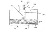
FIG. 11 shows a sectional structure of a typical element according to the present invention, and FIG. 12 shows a planar layout thereof. Since the wiring structure of this element and the manufacturing method thereof are the same as those of a normal LSI, FIG. 11 shows the structure at the end of the formation of the element basic part, and omits the so-called wiring layer between elements. . In FIG. 11,
[0069]
In this structure, there is no unnecessary junction other than the channel shown in FIG. 2, and the insulating
[0070]
The manufacturing process will be described below with reference to FIGS.
[0071]
A
Tungsten is deposited on the substrate surface, and the tungsten deposited other than the grooves 102 and 103 is removed by CMP (Chemical Mechanical Polishing). This process is known as the damascene method. Thereby, a structure in which tungsten 600 is filled in the grooves 102 and 103 is obtained. (Fig. 6)
Further, after the titanium oxide is deposited, a nickel thin film is deposited. After that, by depositing amorphous silicon and applying a low temperature heat treatment at 550 ° C., nickel can be moved in the silicon and the
[0072]
Patterning is performed using a photoresist to process polycrystalline silicon, titanium oxide, and titanium, and the surface of the
[0073]
The
A
Further, a gate pattern using a usual photoresist is formed on the substrate. Then, the
After depositing a 5 nm
Thereafter, the wiring is formed in the same manner as a normal LSI manufacturing process.
[0074]
FIG. 12 is a diagram showing a planar layout of a contact region for extraction from the main part of the semiconductor device. A
[0075]
Further, when polycrystalline silicon doped at a high concentration is used for the
[0076]
In the above embodiment, the
[0077]
In this example, it is manufactured in the same manner as in FIGS. That is, the
A gate pattern using a usual photoresist is formed on the base. Then, the stacked film is etched by the etching method using the gate pattern until the surface of the
Next, after depositing an
Further, a gate pattern using a usual photoresist is formed on the substrate. Then, a
In order to show the effectiveness when this element is used in an integrated circuit, an example of forming an OR circuit and an AND circuit (or a NAND circuit), which are representative operation gates, is shown.
[0078]
FIG. 18 is an equivalent circuit diagram showing a 4-input OR circuit. FIG. 19 is a diagram showing a planar layout of the corresponding electrode portion. In FIG. 19, only the
[0079]
Although the circuit itself shown in FIG. 18 is a usual one, the present invention is characterized by the structure of the channel region of the insulated gate field effect transistor and the extraction structure of each part constituting the circuit. In order to facilitate understanding in the figure, the channel region of the insulated gate field effect transistor according to the present invention is indicated by a wavy line.
[0080]
FIG. 20 is an equivalent circuit diagram of a 3-input AND circuit. FIG. 21 is a diagram showing a planar layout of the electrode portion corresponding to this. By connecting the
[0081]
As described above, a complementary element such as a CMOS can be formed by selecting impurities using the structure of the present invention. That is, in the structure of the present invention, the conductivity type of the impurity to be doped can be changed by the ion implantation method when the
[0082]
FIG. 22 is a diagram illustrating a planar layout of an electrode portion of an example of an inverter. In this example, the structure of the semiconductor device of the present invention is used, and an inverter is formed by using each element whose channel region is N-type and P-type. Of the two
[0083]
FIG. 23 is a diagram showing a planar layout of electrode portions showing a state where two stages of inverters are connected. That is, the structure of FIG. 23 is a structure in which the structure of FIG. 22 is connected in two stages. Two inverters are connected by overlapping the
[0084]
In the process, the
[0085]
In the element structure of the present invention, since a vertical structure is used, formation of the lead wiring from the
[0086]
A laminated body similar to that shown in FIG. 13 is obtained by the steps described in the manufacturing method of the present invention. That is, an insulating
After forming the gate insulating film on the substrate thus prepared, the
Next, an insulating
Thus, an
A mask having an opening is applied to a region corresponding to the lead formation portion, and a groove is formed using the regions of the insulating
Lead wires are formed by embedding
The semiconductor device of the present invention is characterized in that electrode leakage can be suppressed to a very low level. In order to take advantage of this feature, in general, application to a memory element that stores information by electric charge is preferable. In particular, an excellent semiconductor memory device can be provided by using a type called a gain cell.
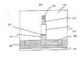
[0087]
FIG. 30 is a cross-sectional view of an application example of the semiconductor device according to the present invention in a gain cell schematically showing only main parts. The memory cell is composed of a reading unit using elements formed on the
[0088]
[0089]
A
[0090]
Examples of basic circuit configurations of typical memory elements are shown in FIGS. Next, the operation of these memory cells will be described.
[0091]
31 is a circuit diagram of a memory cell equivalently showing the semiconductor element shown in FIG. In order to facilitate understanding of the circuit, the reference numerals of the respective parts shown in the structural diagram of FIG. 30 are given to the two transistors T1 and T2 of FIG. The transistor constituting the element T1 reading unit, the element T2, is a stored information writing unit using the semiconductor device according to the present invention.
[0092]
D1 is a read word line, D2 is a write word line, D3 is a write data line, and D4 is a read data line. By turning on D2, the D3 potential is written to the memory holding portion (gate electrode) and turned off to hold the charge. At this time, the gate potential of the reading element is determined. For example, when the gate potential exceeds the threshold value of the transistor, a current flows when a potential difference is applied between D1 and D4. On the other hand, when the gate potential is lower than the threshold value, no current flows even if a potential difference is applied between D1 and D4. Therefore, the gate potential can be read by this current.
[0093]
FIG. 59 is a time chart of an example of each signal in the above example. D1, D2, D3, and D4 indicate voltage application to the read word line, the write word line, the write data line, and the read data line, respectively. Here, the wiring symbols shown in FIG. 31 are used. FIG. 59 shows an example in which the same conductivity type element is written and writing (tw) and reading (tr) by the memory cell used for the reading element are repeated. Here, an example is shown in which the change in potential of D4 is read and driven by a sense amplifier during reading. D4 shows an example in which an intermediate potential is once applied before the tr step and read by a change from the intermediate potential.
[0094]
In this structure, since the writing unit and the reading unit are separated in operation, there is no problem that the reading operation destroys information of other cells even if they are integrated. In the equivalent circuit diagram shown in FIG. 31, D1 and D2, D3 and D4 are arranged so as to be geometrically parallel for each group. However, in the actual structure of the semiconductor device, it is sufficient that at least D1 and D4 and D2 and D3 are arranged so as to be geometrically orthogonal. D1 and D2, and D3 and D4 do not necessarily have to be arranged geometrically in parallel. This is because reading and writing are separated.
[0095]
In FIG. 32, the write and read word lines are shared by D4. In order to explain the operation, the
[0096]
D1 and D3 are read data lines, D2 is a write data line, and D4 is a word line. When the writing element and the reading element are formed with opposite conductivity types, they can be operated in a complementary manner. For example, when the writing element is a P-type and the reading element is an N-type, the writing element is turned on by applying a negative potential to the word line D4, and the potential is written. On the other hand, in the reading element, the channel is turned on by applying a positive potential. That is, by applying a positive potential to D4, a positive potential can be applied to the gate of the reading element by capacitive coupling. At this time, in the writing element, an off state is further increased, so that charge leakage can be suppressed. Since the conventional gain cell could not perform complementary operation, it was necessary to read at a lower voltage than that in order to give the highest gate voltage during writing (erasing) and not destroy the information. Therefore, the potential range that can be used as information is narrow, and it is difficult to have multi-value information. In complementary operation, since there is no such restriction on the word line potential at the time of reading, multi-value information (multi-level potential state) can be used.
[0097]
FIG. 60 shows a time chart of the basic operation of the complementary memory cell. Here, D2 is biased in the opposite direction during writing (tw) and reading (tr). FIG. 60 shows an example in which four-value potentials are sequentially written to the storage node and the read operation is repeated. Here, an example is shown in which a D4ha current sense is applied to operate at a constant potential. D1 and D3 are read data lines, D2 is a write data line, and D4 is a voltage for a word line. As seen in the voltage state of D3, for example, it is possible to use substantially quaternary information.
[0098]
In addition, since the gate potential at the time of reading is not restricted by data destruction, an applied potential can be freely applied. Therefore, the held charge state can be read as a continuous state, not digitized. Further, since the read result is given by the gate application voltage and the held charge state, the arithmetic processing can be performed using this.
[0099]
FIG. 33 shows an example in which the memory cells in FIG. 31 are arranged in an array. C0 is a write word line driver unit, C1 is a write data line driver unit, C2 is a read word line driver unit, and C3 is a read data line sense unit. Since each memory cell portion in FIG. 33 has been described above, details are omitted here. In this example, the usual driving method of the memory device can be taken.
[0100]
The suppression of the leakage current in the structure of the semiconductor device of the present invention is realized by effectively controlling the tunnel phenomenon of the insulating film sandwiched between the electrode and the channel portion by the gate electrode. In other words, maintaining the potential relationship between the write element gate and the drain electrode that is the memory holding portion is important in reducing leakage current. Therefore, in this memory device application, it is effective to provide a device R that can stabilize the write word line in a certain potential state. For this means, it is sufficient to connect a resistor as the device R, for example, as described above. By this means R, the potential of the write word line can be normally set to the ground potential.
[0101]
That is, even when this storage device is disconnected from the power supply, the word line is fixed at the ground potential and the leakage current can be suppressed, so that information can be retained for a long time. When a resistor is used as the device R, the power consumption is increased in the operating state, that is, in the state where the word line is selected. However, the selected word line is one in the array at the maximum and has an appropriate size. By selecting this resistance, good information retention characteristics can be obtained without increasing the power consumption.
[0102]
Even if the memory cell shown in FIG. 32 is used, a memory cell array can be formed similarly to FIG. On the other hand, as shown in FIG. 34, it is effective to build a so-called NAND type array in which multistage memory cells are stacked. This is because the cells that are connected to the same read data lines B0, B1, and B2 can be turned on by sequentially applying voltages from A0 to A7 because they can be operated in a complementary manner. Therefore, since the data line is formed by the diffusion layer and the channel, the formation of wiring and contacts can be reduced. Therefore, miniaturization of the memory cell is facilitated and high integration can be achieved.
[0103]
A process for forming a representative memory cell will be described with reference to FIGS. These drawings show the cross-sectional structure of the semiconductor memory device. In addition, the figure shows a situation in different cross sections on the left and right sides with a gap in the center. In the left cross-sectional view of the figure, the
[0104]
An element
The
An
The
A
Next, another memory cell formation method different from the above will be described with reference to FIGS. In these drawings, the two cross-sectional structures are shown together as described above.
[0105]
A
The laminated film is processed into the
The laminated film is processed by the word line pattern in the word line direction orthogonal to the data line. (Fig. 43)
After forming the
An
The electrode
In this memory cell, the
[0106]
Further, another method for forming a memory cell will be described with reference to FIGS. FIG. 48 is a layout of a semiconductor memory device in which the memory cells shown in FIG. 31 are arranged in an array. Here, 12 cells are shown. D1, D2, D3, and D4 in FIG. 48 each correspond to that in FIG. That is, D1 represents a read word line, D2 represents a write word line, D3 represents a write data line, and D4 represents a read data line. In the figure, each data line, each word line, contact hole, and impurity diffusion region in the substrate are schematically shown. The read word line D1 and the read data line D4 represented by thin lines are arranged in the lower layer of the semiconductor stacked body, and the write word line D2 represented by a thick line is arranged in the upper layer. The hatched region is an impurity diffusion region. A
[0107]
FIGS. 49 to 58 show the AA and BB cross sections in FIG. 48 separately on the left and right, respectively.
[0108]
49 to 58 show a method of forming a memory cell using an SOI (Silicon On Insulator) substrate. Of course, it is obvious that the read element can be formed on the SOI substrate also in the memory cell.
[0109]
First, a wafer having a silicon layer (SOI) 100 and an oxide film as a
An
An opening 901 corresponding to the contact formation portion is formed in the
A
Next, after an
Next, the interlayer film in the writing element formation portion is removed, and an
Further, after forming the
The
A
A
By these methods described above, a semiconductor memory device having excellent writing and memory holding performance can be formed.
[0110]
In a field effect transistor, an insulating film is sandwiched between Schottky junctions and the tunneling phenomenon is controlled, so that the leakage current of the source and drain electrodes can be suppressed to a very low level. Further, by applying this low leakage characteristic, a semiconductor memory device having excellent information retention characteristics can be formed.
[0111]
As described above, according to the present invention, a field effect transistor with extremely low leakage current can be provided.
[0112]
According to another aspect of the present invention, a semiconductor memory device having excellent information retention characteristics can be provided.
[0113]
According to the manufacturing method of the present invention, a novel device can be easily manufactured as a field effect transistor or a semiconductor memory device with extremely low leakage current.
[0114]
【The invention's effect】
According to the present invention, a field effect transistor with extremely low leakage current can be provided.
[0115]
According to another aspect of the present invention, a semiconductor memory device having excellent information retention characteristics can be provided.
[0116]
According to the manufacturing method of the present invention, a novel device can be easily manufactured as a field effect transistor or a semiconductor memory device with extremely low leakage current.
[Brief description of the drawings]
FIG. 1 is a typical element cross-sectional view showing a conventional element structure.
FIG. 2 is a cross-sectional structure diagram schematically showing another conventional element structure.
FIG. 3 is a band diagram for explaining a conventional Schottky junction.
FIG. 4 is a band diagram illustrating bonding used in the present invention.
FIG. 5 is a cross-sectional structure diagram illustrating an element manufacturing process.
FIG. 6 is a cross-sectional structure diagram illustrating an element manufacturing process.
FIG. 7 is a cross-sectional structure diagram illustrating an element manufacturing process.
FIG. 8 is a cross-sectional structure diagram illustrating an element manufacturing process.
FIG. 9 is a cross-sectional structure diagram illustrating an element manufacturing process.
FIG. 10 is a cross-sectional structure diagram illustrating an element manufacturing process.
FIG. 11 is a cross-sectional structure diagram illustrating an element manufacturing process.
FIG. 12 is a plane layout diagram for explaining the element plane arrangement;
FIG. 13 is a cross-sectional structure diagram for explaining another embodiment of a device manufacturing process.
FIG. 14 is a cross-sectional structure diagram for explaining another embodiment of a device manufacturing process.
FIG. 15 is a cross-sectional structure diagram for explaining another element manufacturing process;
FIG. 16 is a cross-sectional structure diagram for explaining another element manufacturing process;
FIG. 17 is a cross-sectional structure diagram for explaining an element manufacturing process of another form;
FIG. 18 is an equivalent circuit diagram illustrating an OR gate.
FIG. 19 is a planar layout diagram for explaining the planar arrangement of OR gates.
FIG. 20 is an equivalent circuit diagram for explaining an AND gate;
FIG. 21 is a plan layout diagram for explaining a plane layout of AND gates;
FIG. 22 is a plan layout diagram illustrating a planar layout of inverter gates.
FIG. 23 is a plan layout diagram illustrating a planar layout of a multi-stage inverter gate.
FIG. 24 is a cross-sectional structure diagram for explaining another element manufacturing process;
FIG. 25 is a cross-sectional structure diagram for explaining another element manufacturing process;
FIG. 26 is a cross-sectional structure diagram for explaining another element manufacturing process;
FIG. 27 is a cross-sectional structure diagram for explaining another element manufacturing process;
FIG. 28 is a cross-sectional structure diagram illustrating another element manufacturing process.
FIG. 29 is a cross-sectional structure diagram for explaining another element manufacturing process;
FIG. 30 is a cross-sectional structure diagram schematically showing a memory cell element structure.
FIG. 31 is an equivalent circuit diagram for explaining a memory cell;
FIG. 32 is an equivalent circuit diagram illustrating another memory cell.
FIG. 33 is an equivalent circuit diagram illustrating a memory cell array.
FIG. 34 is an equivalent circuit diagram illustrating a memory cell array.
FIG. 35 is a cross-sectional structure diagram illustrating an element manufacturing process of a memory cell.
FIG. 36 is a cross-sectional structure diagram illustrating an element manufacturing process of a memory cell.
FIG. 37 is a cross-sectional structure diagram illustrating an element manufacturing process of a memory cell.
FIG. 38 is a cross-sectional structure diagram illustrating an element manufacturing process of a memory cell.
FIG. 39 is a cross-sectional structure diagram illustrating an element manufacturing process of a memory cell.
FIG. 40 is a cross-sectional structure diagram illustrating an element manufacturing process of a memory cell.
FIG. 41 is a cross-sectional structure diagram illustrating an element manufacturing process of another memory cell.
FIG. 42 is a cross-sectional structure diagram illustrating a manufacturing process of another memory cell element.
FIG. 43 is a cross-sectional structure diagram illustrating a manufacturing process of another memory cell element.
FIG. 44 is a cross-sectional structure diagram for explaining an element manufacturing process of another memory cell;
FIG. 45 is a cross-sectional structure diagram for explaining an element manufacturing process of another memory cell;
FIG. 46 is a cross-sectional structure diagram for explaining an element manufacturing process of another memory cell;
FIG. 47 is a cross-sectional structure diagram for explaining an element manufacturing process of another memory cell;
FIG. 48 is a plan layout diagram for explaining a planar layout of a memory cell array;
FIG. 49 is a plan layout diagram for explaining a planar layout of a multi-stage inverter gate.
FIG. 50 is a plan layout diagram illustrating a planar layout of a multi-stage inverter gate.
FIG. 51 is a plan layout diagram for explaining a planar layout of a multistage inverter gate;
FIG. 52 is a plan layout diagram for explaining a planar layout of a multi-stage inverter gate.
FIG. 53 is a plan layout diagram for explaining a planar layout of a multi-stage inverter gate;
FIG. 54 is a plan layout diagram for explaining a planar layout of a multistage inverter gate;
FIG. 55 is a plan layout diagram for explaining a planar layout of a multi-stage inverter gate.
FIG. 56 is a plan layout diagram for explaining a planar layout of a multi-stage inverter gate.
FIG. 57 is a plan layout diagram for explaining a planar layout of a multistage inverter gate;
FIG. 58 is a plan layout diagram for explaining a planar layout of a multistage inverter gate.
FIG. 59 is a diagram showing a time chart for the basic operation of the semiconductor memory.
FIG. 60 is a diagram showing a time chart for the basic operation of a semiconductor memory device handling multi-value information.
[Explanation of symbols]
100, 110: silicon substrate, 150: polycrystalline silicon, 320: impurity diffusion layer electrode, 500, 510: gate electrode, 250, 350: electrode, 600, 625, 660: metal wiring, 710, 720, 730: contact, 900, 901, 905, 910, 920, 921, 922, 923, 924, 925, 926, 931, 932, 955, 956, 960, 980: insulating film layers.
Claims (6)
Translated fromJapanesePriority Applications (1)
| Application Number | Priority Date | Filing Date | Title |
|---|---|---|---|
| JP2000143424AJP3936830B2 (en) | 1999-05-13 | 2000-05-11 | Semiconductor device |
Applications Claiming Priority (3)
| Application Number | Priority Date | Filing Date | Title |
|---|---|---|---|
| JP13233299 | 1999-05-13 | ||
| JP11-132332 | 1999-05-13 | ||
| JP2000143424AJP3936830B2 (en) | 1999-05-13 | 2000-05-11 | Semiconductor device |
Publications (3)
| Publication Number | Publication Date |
|---|---|
| JP2001028443A JP2001028443A (en) | 2001-01-30 |
| JP2001028443A5 JP2001028443A5 (en) | 2005-01-06 |
| JP3936830B2true JP3936830B2 (en) | 2007-06-27 |
Family
ID=26466940
Family Applications (1)
| Application Number | Title | Priority Date | Filing Date |
|---|---|---|---|
| JP2000143424AExpired - Fee RelatedJP3936830B2 (en) | 1999-05-13 | 2000-05-11 | Semiconductor device |
Country Status (1)
| Country | Link |
|---|---|
| JP (1) | JP3936830B2 (en) |
Families Citing this family (32)
| Publication number | Priority date | Publication date | Assignee | Title |
|---|---|---|---|---|
| JP2003068883A (en)* | 2001-08-24 | 2003-03-07 | Hitachi Ltd | Semiconductor storage device |
| JP2004221242A (en) | 2003-01-14 | 2004-08-05 | Renesas Technology Corp | Semiconductor integrated circuit device and method of manufacturing the same |
| JP2004253730A (en) | 2003-02-21 | 2004-09-09 | Renesas Technology Corp | Semiconductor integrated circuit device and its manufacturing method |
| US6830963B1 (en)* | 2003-10-09 | 2004-12-14 | Micron Technology, Inc. | Fully depleted silicon-on-insulator CMOS logic |
| WO2009110050A1 (en)* | 2008-02-15 | 2009-09-11 | 日本ユニサンティスエレクトロニクス株式会社 | Method for manufacturing semiconductor device |
| JP5583933B2 (en)* | 2009-07-28 | 2014-09-03 | 猛英 白土 | Semiconductor device and manufacturing method thereof |
| CN102576708B (en) | 2009-10-30 | 2015-09-23 | 株式会社半导体能源研究所 | Semiconductor device |
| WO2011052367A1 (en) | 2009-10-30 | 2011-05-05 | Semiconductor Energy Laboratory Co., Ltd. | Semiconductor device |
| WO2011055660A1 (en) | 2009-11-06 | 2011-05-12 | Semiconductor Energy Laboratory Co., Ltd. | Semiconductor device |
| KR101448908B1 (en)* | 2009-11-20 | 2014-10-15 | 가부시키가이샤 한도오따이 에네루기 켄큐쇼 | Semiconductor device |
| WO2011065258A1 (en)* | 2009-11-27 | 2011-06-03 | Semiconductor Energy Laboratory Co., Ltd. | Semiconductor device |
| KR101798367B1 (en)* | 2010-01-15 | 2017-11-16 | 가부시키가이샤 한도오따이 에네루기 켄큐쇼 | Semiconductor device |
| KR101948707B1 (en)* | 2010-01-29 | 2019-02-15 | 가부시키가이샤 한도오따이 에네루기 켄큐쇼 | Semiconductor memory device |
| WO2011096262A1 (en)* | 2010-02-05 | 2011-08-11 | Semiconductor Energy Laboratory Co., Ltd. | Semiconductor device |
| WO2011114868A1 (en) | 2010-03-19 | 2011-09-22 | Semiconductor Energy Laboratory Co., Ltd. | Semiconductor device |
| KR101891065B1 (en) | 2010-03-19 | 2018-08-24 | 가부시키가이샤 한도오따이 에네루기 켄큐쇼 | Semiconductor device and driving method of semiconductor device |
| US8588000B2 (en) | 2010-05-20 | 2013-11-19 | Semiconductor Energy Laboratory Co., Ltd. | Semiconductor memory device having a reading transistor with a back-gate electrode |
| CN102339828B (en)* | 2010-07-19 | 2013-04-24 | 中国科学院微电子研究所 | Low power consumption semiconductor memory and driving method thereof |
| TWI545587B (en) | 2010-08-06 | 2016-08-11 | 半導體能源研究所股份有限公司 | Semiconductor device and method for driving semiconductor device |
| US8467232B2 (en)* | 2010-08-06 | 2013-06-18 | Semiconductor Energy Laboratory Co., Ltd. | Semiconductor device |
| US8467231B2 (en)* | 2010-08-06 | 2013-06-18 | Semiconductor Energy Laboratory Co., Ltd. | Semiconductor device and driving method thereof |
| US8422272B2 (en) | 2010-08-06 | 2013-04-16 | Semiconductor Energy Laboratory Co., Ltd. | Semiconductor device and driving method thereof |
| US8520426B2 (en)* | 2010-09-08 | 2013-08-27 | Semiconductor Energy Laboratory Co., Ltd. | Method for driving semiconductor device |
| KR101952733B1 (en) | 2010-11-05 | 2019-02-27 | 가부시키가이샤 한도오따이 에네루기 켄큐쇼 | Semiconductor device |
| JP6013682B2 (en) | 2011-05-20 | 2016-10-25 | 株式会社半導体エネルギー研究所 | Driving method of semiconductor device |
| JP2013125102A (en)* | 2011-12-13 | 2013-06-24 | Samsung Yokohama Research Institute Co Ltd | Optical filter, polarization element and optical shutter using fine periodic structure |
| JP6100559B2 (en)* | 2012-03-05 | 2017-03-22 | 株式会社半導体エネルギー研究所 | Semiconductor memory device |
| JP2014179465A (en)* | 2013-03-14 | 2014-09-25 | Toshiba Corp | Nonvolatile semiconductor storage device and manufacturing method of the same |
| WO2016092416A1 (en) | 2014-12-11 | 2016-06-16 | Semiconductor Energy Laboratory Co., Ltd. | Semiconductor device, memory device, and electronic device |
| US9773787B2 (en)* | 2015-11-03 | 2017-09-26 | Semiconductor Energy Laboratory Co., Ltd. | Semiconductor device, memory device, electronic device, or method for driving the semiconductor device |
| JP6822853B2 (en)* | 2016-01-21 | 2021-01-27 | 株式会社半導体エネルギー研究所 | Storage device and driving method of storage device |
| CN116981246A (en)* | 2022-04-15 | 2023-10-31 | 华为技术有限公司 | Memory array and preparation method thereof |
- 2000
- 2000-05-11JPJP2000143424Apatent/JP3936830B2/ennot_activeExpired - Fee Related
Also Published As
| Publication number | Publication date |
|---|---|
| JP2001028443A (en) | 2001-01-30 |
Similar Documents
| Publication | Publication Date | Title |
|---|---|---|
| JP3936830B2 (en) | Semiconductor device | |
| US6873009B2 (en) | Vertical semiconductor device with tunnel insulator in current path controlled by gate electrode | |
| US9136376B2 (en) | Semiconductor device having junctionless vertical gate transistor and method of manufacturing the same | |
| JP3744938B2 (en) | Fabrication of a device having a self-amplifying dynamic MOS transistor memory cell. | |
| CN100468621C (en) | Integrated circuit device comprising a capacitor and method of manufacturing | |
| CN114420644A (en) | Semiconductor structure and method of making the same | |
| TW200843111A (en) | Floating body memory cell having gates favoring different conductivity type regions | |
| US11195842B2 (en) | Vertical non-volatile memory structure with additional bitline in wordline stack | |
| US20230397399A1 (en) | Semiconductor structure and manufacturing method thereof | |
| CN114725106A (en) | Semiconductor structure, preparation method of semiconductor structure and memory | |
| JP2851968B2 (en) | Semiconductor device having improved insulated gate transistor and method of manufacturing the same | |
| KR101458332B1 (en) | Semiconductor device, method for manufacturing same, and nonvolatile semiconductor memory device | |
| CN115411033A (en) | Semiconductor structure and manufacturing method thereof | |
| TWI813363B (en) | Semiconductor structure and method of manufacturing the same | |
| CN116504785A (en) | Semiconductor device and method of manufacturing the same | |
| KR20230062467A (en) | Semiconductor structure and manufacturing method thereof | |
| KR100237900B1 (en) | Semiconductor storage device | |
| JP4014873B2 (en) | SOI DRAM without substrate floating effect | |
| JP2001068633A (en) | Ferroelectric nonvolatile memory | |
| TWI802451B (en) | Semiconductor structure and method for manufacturing semiconductor structure | |
| CN119110579B (en) | Memory cell structure, memory cell array and manufacturing method thereof | |
| CN116033740B (en) | Semiconductor structure and manufacturing method thereof | |
| US20250311194A1 (en) | Semiconductor devices and fabricating methods thereof | |
| US20250311242A1 (en) | Memory device and operation method thereof | |
| CN117881178A (en) | Semiconductor structure and preparation method thereof |
Legal Events
| Date | Code | Title | Description |
|---|---|---|---|
| A521 | Request for written amendment filed | Free format text:JAPANESE INTERMEDIATE CODE: A523 Effective date:20040209 | |
| A621 | Written request for application examination | Free format text:JAPANESE INTERMEDIATE CODE: A621 Effective date:20040209 | |
| A131 | Notification of reasons for refusal | Free format text:JAPANESE INTERMEDIATE CODE: A131 Effective date:20051129 | |
| A521 | Request for written amendment filed | Free format text:JAPANESE INTERMEDIATE CODE: A523 Effective date:20060112 | |
| RD02 | Notification of acceptance of power of attorney | Free format text:JAPANESE INTERMEDIATE CODE: A7422 Effective date:20060112 | |
| A131 | Notification of reasons for refusal | Free format text:JAPANESE INTERMEDIATE CODE: A131 Effective date:20061205 | |
| A521 | Request for written amendment filed | Free format text:JAPANESE INTERMEDIATE CODE: A523 Effective date:20070202 | |
| TRDD | Decision of grant or rejection written | ||
| A01 | Written decision to grant a patent or to grant a registration (utility model) | Free format text:JAPANESE INTERMEDIATE CODE: A01 Effective date:20070227 | |
| A61 | First payment of annual fees (during grant procedure) | Free format text:JAPANESE INTERMEDIATE CODE: A61 Effective date:20070326 | |
| R150 | Certificate of patent or registration of utility model | Free format text:JAPANESE INTERMEDIATE CODE: R150 | |
| FPAY | Renewal fee payment (event date is renewal date of database) | Free format text:PAYMENT UNTIL: 20110330 Year of fee payment:4 | |
| FPAY | Renewal fee payment (event date is renewal date of database) | Free format text:PAYMENT UNTIL: 20110330 Year of fee payment:4 | |
| FPAY | Renewal fee payment (event date is renewal date of database) | Free format text:PAYMENT UNTIL: 20120330 Year of fee payment:5 | |
| FPAY | Renewal fee payment (event date is renewal date of database) | Free format text:PAYMENT UNTIL: 20130330 Year of fee payment:6 | |
| FPAY | Renewal fee payment (event date is renewal date of database) | Free format text:PAYMENT UNTIL: 20130330 Year of fee payment:6 | |
| FPAY | Renewal fee payment (event date is renewal date of database) | Free format text:PAYMENT UNTIL: 20140330 Year of fee payment:7 | |
| LAPS | Cancellation because of no payment of annual fees |