JP3929140B2 - Corrosion resistant member and manufacturing method thereof - Google Patents
Corrosion resistant member and manufacturing method thereofDownload PDFInfo
- Publication number
- JP3929140B2 JP3929140B2JP29421197AJP29421197AJP3929140B2JP 3929140 B2JP3929140 B2JP 3929140B2JP 29421197 AJP29421197 AJP 29421197AJP 29421197 AJP29421197 AJP 29421197AJP 3929140 B2JP3929140 B2JP 3929140B2
- Authority
- JP
- Japan
- Prior art keywords
- silicon carbide
- carbide film
- film
- corrosion
- temperature
- Prior art date
- Legal status (The legal status is an assumption and is not a legal conclusion. Google has not performed a legal analysis and makes no representation as to the accuracy of the status listed.)
- Expired - Fee Related
Links
- 238000005260corrosionMethods0.000titleclaimsdescription30
- 230000007797corrosionEffects0.000titleclaimsdescription30
- 238000004519manufacturing processMethods0.000titleclaimsdescription20
- HBMJWWWQQXIZIP-UHFFFAOYSA-Nsilicon carbideChemical compound[Si+]#[C-]HBMJWWWQQXIZIP-UHFFFAOYSA-N0.000claimsdescription96
- 229910010271silicon carbideInorganic materials0.000claimsdescription96
- 239000000758substrateSubstances0.000claimsdescription42
- 239000000463materialSubstances0.000claimsdescription28
- 239000007789gasSubstances0.000claimsdescription25
- 238000005229chemical vapour depositionMethods0.000claimsdescription23
- 239000000919ceramicSubstances0.000claimsdescription20
- XKRFYHLGVUSROY-UHFFFAOYSA-NArgonChemical compound[Ar]XKRFYHLGVUSROY-UHFFFAOYSA-N0.000claimsdescription16
- 230000015572biosynthetic processEffects0.000claimsdescription14
- XUIMIQQOPSSXEZ-UHFFFAOYSA-NSiliconChemical compound[Si]XUIMIQQOPSSXEZ-UHFFFAOYSA-N0.000claimsdescription11
- 238000000034methodMethods0.000claimsdescription11
- 239000003518causticsSubstances0.000claimsdescription10
- 238000010438heat treatmentMethods0.000claimsdescription10
- 229910052786argonInorganic materials0.000claimsdescription8
- 229910052710siliconInorganic materials0.000claimsdescription8
- 239000010703siliconSubstances0.000claimsdescription8
- 229910052751metalInorganic materials0.000claimsdescription3
- 239000002184metalSubstances0.000claimsdescription3
- 239000000126substanceSubstances0.000claimsdescription3
- 239000010408filmSubstances0.000description89
- 239000012159carrier gasSubstances0.000description11
- 150000001875compoundsChemical class0.000description10
- VNWKTOKETHGBQD-UHFFFAOYSA-NmethaneChemical compoundCVNWKTOKETHGBQD-UHFFFAOYSA-N0.000description10
- 230000000052comparative effectEffects0.000description9
- 239000001257hydrogenSubstances0.000description9
- 229910052739hydrogenInorganic materials0.000description9
- 230000035939shockEffects0.000description8
- UFHFLCQGNIYNRP-UHFFFAOYSA-NHydrogenChemical compound[H][H]UFHFLCQGNIYNRP-UHFFFAOYSA-N0.000description7
- 238000002474experimental methodMethods0.000description7
- 239000002994raw materialSubstances0.000description7
- OKTJSMMVPCPJKN-UHFFFAOYSA-NCarbonChemical compound[C]OKTJSMMVPCPJKN-UHFFFAOYSA-N0.000description5
- 229910052799carbonInorganic materials0.000description5
- 239000011248coating agentSubstances0.000description5
- 238000000576coating methodMethods0.000description5
- 238000001816coolingMethods0.000description5
- 210000002381plasmaAnatomy0.000description5
- VXEGSRKPIUDPQT-UHFFFAOYSA-N4-[4-(4-methoxyphenyl)piperazin-1-yl]anilineChemical compoundC1=CC(OC)=CC=C1N1CCN(C=2C=CC(N)=CC=2)CC1VXEGSRKPIUDPQT-UHFFFAOYSA-N0.000description4
- VEXZGXHMUGYJMC-UHFFFAOYSA-NHydrochloric acidChemical compoundClVEXZGXHMUGYJMC-UHFFFAOYSA-N0.000description4
- 238000000151depositionMethods0.000description4
- 239000005049silicon tetrachlorideSubstances0.000description4
- 230000008021depositionEffects0.000description3
- 239000011261inert gasSubstances0.000description3
- 239000004065semiconductorSubstances0.000description3
- 239000010409thin filmSubstances0.000description3
- KRHYYFGTRYWZRS-UHFFFAOYSA-NFluoraneChemical compoundFKRHYYFGTRYWZRS-UHFFFAOYSA-N0.000description2
- 229910003902SiCl 4Inorganic materials0.000description2
- 238000007664blowingMethods0.000description2
- 238000006243chemical reactionMethods0.000description2
- 230000000694effectsEffects0.000description2
- 150000002431hydrogenChemical class0.000description2
- 230000002093peripheral effectEffects0.000description2
- VZGDMQKNWNREIO-UHFFFAOYSA-NtetrachloromethaneChemical compoundClC(Cl)(Cl)ClVZGDMQKNWNREIO-UHFFFAOYSA-N0.000description2
- XLYOFNOQVPJJNP-UHFFFAOYSA-NwaterSubstancesOXLYOFNOQVPJJNP-UHFFFAOYSA-N0.000description2
- GRYLNZFGIOXLOG-UHFFFAOYSA-NNitric acidChemical compoundO[N+]([O-])=OGRYLNZFGIOXLOG-UHFFFAOYSA-N0.000description1
- 238000002441X-ray diffractionMethods0.000description1
- 239000002253acidSubstances0.000description1
- 150000007513acidsChemical class0.000description1
- 230000003373anti-fouling effectEffects0.000description1
- QZPSXPBJTPJTSZ-UHFFFAOYSA-Naqua regiaChemical compoundCl.O[N+]([O-])=OQZPSXPBJTPJTSZ-UHFFFAOYSA-N0.000description1
- SLLGVCUQYRMELA-UHFFFAOYSA-NchlorosiliconChemical compoundCl[Si]SLLGVCUQYRMELA-UHFFFAOYSA-N0.000description1
- 238000011109contaminationMethods0.000description1
- 238000005336crackingMethods0.000description1
- 239000013078crystalSubstances0.000description1
- 230000002950deficientEffects0.000description1
- 238000001514detection methodMethods0.000description1
- 238000009826distributionMethods0.000description1
- 238000005530etchingMethods0.000description1
- 229910001385heavy metalInorganic materials0.000description1
- 239000012535impuritySubstances0.000description1
- 150000002500ionsChemical class0.000description1
- 229910021645metal ionInorganic materials0.000description1
- 229910017604nitric acidInorganic materials0.000description1
- 238000004544sputter depositionMethods0.000description1
- 238000010301surface-oxidation reactionMethods0.000description1
- 238000007751thermal sprayingMethods0.000description1
- 229910021642ultra pure waterInorganic materials0.000description1
- 239000012498ultrapure waterSubstances0.000description1
- 238000007740vapor depositionMethods0.000description1
- 239000012808vapor phaseSubstances0.000description1
Images


Classifications
- C—CHEMISTRY; METALLURGY
- C23—COATING METALLIC MATERIAL; COATING MATERIAL WITH METALLIC MATERIAL; CHEMICAL SURFACE TREATMENT; DIFFUSION TREATMENT OF METALLIC MATERIAL; COATING BY VACUUM EVAPORATION, BY SPUTTERING, BY ION IMPLANTATION OR BY CHEMICAL VAPOUR DEPOSITION, IN GENERAL; INHIBITING CORROSION OF METALLIC MATERIAL OR INCRUSTATION IN GENERAL
- C23C—COATING METALLIC MATERIAL; COATING MATERIAL WITH METALLIC MATERIAL; SURFACE TREATMENT OF METALLIC MATERIAL BY DIFFUSION INTO THE SURFACE, BY CHEMICAL CONVERSION OR SUBSTITUTION; COATING BY VACUUM EVAPORATION, BY SPUTTERING, BY ION IMPLANTATION OR BY CHEMICAL VAPOUR DEPOSITION, IN GENERAL
- C23C16/00—Chemical coating by decomposition of gaseous compounds, without leaving reaction products of surface material in the coating, i.e. chemical vapour deposition [CVD] processes
- C23C16/22—Chemical coating by decomposition of gaseous compounds, without leaving reaction products of surface material in the coating, i.e. chemical vapour deposition [CVD] processes characterised by the deposition of inorganic material, other than metallic material
- C23C16/30—Deposition of compounds, mixtures or solid solutions, e.g. borides, carbides, nitrides
- C23C16/32—Carbides
- C—CHEMISTRY; METALLURGY
- C04—CEMENTS; CONCRETE; ARTIFICIAL STONE; CERAMICS; REFRACTORIES
- C04B—LIME, MAGNESIA; SLAG; CEMENTS; COMPOSITIONS THEREOF, e.g. MORTARS, CONCRETE OR LIKE BUILDING MATERIALS; ARTIFICIAL STONE; CERAMICS; REFRACTORIES; TREATMENT OF NATURAL STONE
- C04B41/00—After-treatment of mortars, concrete, artificial stone or ceramics; Treatment of natural stone
- C04B41/009—After-treatment of mortars, concrete, artificial stone or ceramics; Treatment of natural stone characterised by the material treated
- C—CHEMISTRY; METALLURGY
- C04—CEMENTS; CONCRETE; ARTIFICIAL STONE; CERAMICS; REFRACTORIES
- C04B—LIME, MAGNESIA; SLAG; CEMENTS; COMPOSITIONS THEREOF, e.g. MORTARS, CONCRETE OR LIKE BUILDING MATERIALS; ARTIFICIAL STONE; CERAMICS; REFRACTORIES; TREATMENT OF NATURAL STONE
- C04B41/00—After-treatment of mortars, concrete, artificial stone or ceramics; Treatment of natural stone
- C04B41/45—Coating or impregnating, e.g. injection in masonry, partial coating of green or fired ceramics, organic coating compositions for adhering together two concrete elements
- C04B41/50—Coating or impregnating, e.g. injection in masonry, partial coating of green or fired ceramics, organic coating compositions for adhering together two concrete elements with inorganic materials
- C04B41/5053—Coating or impregnating, e.g. injection in masonry, partial coating of green or fired ceramics, organic coating compositions for adhering together two concrete elements with inorganic materials non-oxide ceramics
- C04B41/5057—Carbides
- C04B41/5059—Silicon carbide
- C—CHEMISTRY; METALLURGY
- C04—CEMENTS; CONCRETE; ARTIFICIAL STONE; CERAMICS; REFRACTORIES
- C04B—LIME, MAGNESIA; SLAG; CEMENTS; COMPOSITIONS THEREOF, e.g. MORTARS, CONCRETE OR LIKE BUILDING MATERIALS; ARTIFICIAL STONE; CERAMICS; REFRACTORIES; TREATMENT OF NATURAL STONE
- C04B41/00—After-treatment of mortars, concrete, artificial stone or ceramics; Treatment of natural stone
- C04B41/80—After-treatment of mortars, concrete, artificial stone or ceramics; Treatment of natural stone of only ceramics
- C04B41/81—Coating or impregnation
- C04B41/85—Coating or impregnation with inorganic materials
- C04B41/87—Ceramics
- C—CHEMISTRY; METALLURGY
- C23—COATING METALLIC MATERIAL; COATING MATERIAL WITH METALLIC MATERIAL; CHEMICAL SURFACE TREATMENT; DIFFUSION TREATMENT OF METALLIC MATERIAL; COATING BY VACUUM EVAPORATION, BY SPUTTERING, BY ION IMPLANTATION OR BY CHEMICAL VAPOUR DEPOSITION, IN GENERAL; INHIBITING CORROSION OF METALLIC MATERIAL OR INCRUSTATION IN GENERAL
- C23C—COATING METALLIC MATERIAL; COATING MATERIAL WITH METALLIC MATERIAL; SURFACE TREATMENT OF METALLIC MATERIAL BY DIFFUSION INTO THE SURFACE, BY CHEMICAL CONVERSION OR SUBSTITUTION; COATING BY VACUUM EVAPORATION, BY SPUTTERING, BY ION IMPLANTATION OR BY CHEMICAL VAPOUR DEPOSITION, IN GENERAL
- C23C16/00—Chemical coating by decomposition of gaseous compounds, without leaving reaction products of surface material in the coating, i.e. chemical vapour deposition [CVD] processes
- C23C16/22—Chemical coating by decomposition of gaseous compounds, without leaving reaction products of surface material in the coating, i.e. chemical vapour deposition [CVD] processes characterised by the deposition of inorganic material, other than metallic material
- C23C16/30—Deposition of compounds, mixtures or solid solutions, e.g. borides, carbides, nitrides
- C23C16/32—Carbides
- C23C16/325—Silicon carbide
- C—CHEMISTRY; METALLURGY
- C23—COATING METALLIC MATERIAL; COATING MATERIAL WITH METALLIC MATERIAL; CHEMICAL SURFACE TREATMENT; DIFFUSION TREATMENT OF METALLIC MATERIAL; COATING BY VACUUM EVAPORATION, BY SPUTTERING, BY ION IMPLANTATION OR BY CHEMICAL VAPOUR DEPOSITION, IN GENERAL; INHIBITING CORROSION OF METALLIC MATERIAL OR INCRUSTATION IN GENERAL
- C23C—COATING METALLIC MATERIAL; COATING MATERIAL WITH METALLIC MATERIAL; SURFACE TREATMENT OF METALLIC MATERIAL BY DIFFUSION INTO THE SURFACE, BY CHEMICAL CONVERSION OR SUBSTITUTION; COATING BY VACUUM EVAPORATION, BY SPUTTERING, BY ION IMPLANTATION OR BY CHEMICAL VAPOUR DEPOSITION, IN GENERAL
- C23C16/00—Chemical coating by decomposition of gaseous compounds, without leaving reaction products of surface material in the coating, i.e. chemical vapour deposition [CVD] processes
- C23C16/56—After-treatment
- C—CHEMISTRY; METALLURGY
- C04—CEMENTS; CONCRETE; ARTIFICIAL STONE; CERAMICS; REFRACTORIES
- C04B—LIME, MAGNESIA; SLAG; CEMENTS; COMPOSITIONS THEREOF, e.g. MORTARS, CONCRETE OR LIKE BUILDING MATERIALS; ARTIFICIAL STONE; CERAMICS; REFRACTORIES; TREATMENT OF NATURAL STONE
- C04B2111/00—Mortars, concrete or artificial stone or mixtures to prepare them, characterised by specific function, property or use
- C04B2111/20—Resistance against chemical, physical or biological attack
- Y—GENERAL TAGGING OF NEW TECHNOLOGICAL DEVELOPMENTS; GENERAL TAGGING OF CROSS-SECTIONAL TECHNOLOGIES SPANNING OVER SEVERAL SECTIONS OF THE IPC; TECHNICAL SUBJECTS COVERED BY FORMER USPC CROSS-REFERENCE ART COLLECTIONS [XRACs] AND DIGESTS
- Y10—TECHNICAL SUBJECTS COVERED BY FORMER USPC
- Y10T—TECHNICAL SUBJECTS COVERED BY FORMER US CLASSIFICATION
- Y10T428/00—Stock material or miscellaneous articles
- Y10T428/24—Structurally defined web or sheet [e.g., overall dimension, etc.]
- Y10T428/24942—Structurally defined web or sheet [e.g., overall dimension, etc.] including components having same physical characteristic in differing degree
- Y10T428/2495—Thickness [relative or absolute]
- Y—GENERAL TAGGING OF NEW TECHNOLOGICAL DEVELOPMENTS; GENERAL TAGGING OF CROSS-SECTIONAL TECHNOLOGIES SPANNING OVER SEVERAL SECTIONS OF THE IPC; TECHNICAL SUBJECTS COVERED BY FORMER USPC CROSS-REFERENCE ART COLLECTIONS [XRACs] AND DIGESTS
- Y10—TECHNICAL SUBJECTS COVERED BY FORMER USPC
- Y10T—TECHNICAL SUBJECTS COVERED BY FORMER US CLASSIFICATION
- Y10T428/00—Stock material or miscellaneous articles
- Y10T428/24—Structurally defined web or sheet [e.g., overall dimension, etc.]
- Y10T428/24942—Structurally defined web or sheet [e.g., overall dimension, etc.] including components having same physical characteristic in differing degree
- Y10T428/24992—Density or compression of components
Landscapes
- Chemical & Material Sciences (AREA)
- Engineering & Computer Science (AREA)
- Ceramic Engineering (AREA)
- Materials Engineering (AREA)
- Organic Chemistry (AREA)
- Inorganic Chemistry (AREA)
- Structural Engineering (AREA)
- General Chemical & Material Sciences (AREA)
- Chemical Kinetics & Catalysis (AREA)
- Mechanical Engineering (AREA)
- Metallurgy (AREA)
- Chemical Vapour Deposition (AREA)
Description
Translated fromJapanese【0001】
【発明の属する技術分野】
本発明は、耐蝕性部材およびその製造方法に関するものである。
【0002】
【従来の技術】
現在、ガスタービン部品、ディーゼルエンジン部品のライナー等、高温雰囲気で使用されるセラミックス部材の表面耐酸化膜として、緻密質の炭化珪素膜が有効であることが知られている。また、他にも半導体製造装置など、幾つかの用途において、セラミックス部材の表面を緻密質の炭化珪素薄膜によって被覆することが知られている。こうした薄膜を形成する方法としては、化学的気相成長法、、電気化学的気相成長法、スパッタリング法、溶射法等が知られている。例えば、気相法によると、高純度で緻密質の良質な薄膜を形成できるので、現在のところ多用されている。
【0003】
近年、超純水や減菌水に加え、ふっ酸、硝酸、塩酸、および王水等の混酸を含む超高純度溶液も、金属イオンや有機物によって全く汚染することなく処理することが求められるようになってきている。また、CF4,NF3,ClF3,HF,HCl,HBr等の反応性プラズマガスに対して暴露される気密部品の需要がある。このような反応性プラズマはいずれも強い腐食性を有している。このような高度に腐食性の溶液、ガスに暴露される環境下で長期間に渡って気密性および汚染防止性を維持できるような部材が要望されている。
【0004】
本発明者は、この問題を解決するために検討してきたが、困難に直面した。即ち、例えば半導体製造装置用の気密部品において、気密部品を長期間にわたって使用できるようにするためには、炭化珪素被膜を厚くする必要がある。一方で、大量に溶液やガスを処理するには大型の容器が必要とされる。このような大型の容器を処理できるようにするためには、焼結体の面積の大きな表面を気密性の炭化珪素被膜によって被覆する必要がある。
【0005】
【発明が解決しようとする課題】
しかし、このような気密部品は、現実には、室温と高温の間で熱衝撃にさらされるが、炭化珪素皮膜を大面積にして厚くした場合、熱衝撃によって炭化珪素皮膜に亀裂が発生し、炭化珪素皮膜の気密性が低下し、下地に含まれる不純物質が溶液やガス中に溶出して汚染するという問題があった。
【0006】
本発明の課題は、セラミックス基材と、この基材の表面を被覆する化学蒸着法によって得られた厚膜の炭化珪素膜とを備えている耐蝕性部材であって、耐蝕性が高く、熱衝撃を加えたときにも炭化珪素皮膜に亀裂の発生しない耐蝕性部材を提供することである。
【0007】
【課題を解決するための手段】
本発明は、少なくとも直径が200mm以上の円盤状の基材であって、炭化珪素の組成比率が90%以上であり且つ相対密度が90%以上であるセラミックスか、炭化珪素の組成比率が90%以上であり且つ相対密度が56%〜90%である多孔質焼結体か、又は炭化珪素と金属シリコンとの混合焼結体である当該基材と、
この基材の表面の40%以上を被覆する厚さ2.1〜8.3mmの化学蒸着炭化珪素からなるクラックのない炭化珪素膜とを備えていることを特徴とする耐蝕性部材に関するものである。
【0008】
また、本発明は、セラミックス基材と、この基材の表面を被覆する炭化珪素膜とを備える耐蝕性部材の製造方法において、この炭化珪素膜を、化学蒸着法により1400℃〜1500℃の成膜温度で成膜し、更にこの炭化珪素膜をアルゴンガス中で前記成膜温度より50℃〜200℃高い温度で1時間以上加熱処理することを特徴とする。
【0009】
本発明者は、種々の形態の炭化珪素焼結体に対して化学蒸着法によって炭化珪素膜を形成し、その耐久性等を検討してきた。この結果、次のような知見に達した。
【0010】
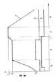
例えば、本発明者は、図1(a)、(b)に示すような耐蝕性容器3を作製した。この容器3は、例えば円盤形状の下側容器2と蓋1とを備えている。蓋1の基材4の内側面4aおよびその周縁部4bが炭化珪素膜5によって被覆されている。下側容器2の基材6の内側面6a、縁面6bが、炭化珪素膜7によって被覆されている。容器3の内側空間8内に、腐食性物質9が収容されている。各基材4、6のうち、容器内の腐食性物質9と接触する面にはすべて炭化珪素膜5a、7aが形成されており、腐食性物質は基材に直接接触しない。容器の直径は特に限定されないが、例えば300mmまたは500mmとし、下側容器の深さを100mmとすることができる。
【0011】
蓋1と下側容器2との接合部分においては、炭化珪素膜5bと6bとが互いに接触しており、すり合わせされており、この接合部分で気密性が保持されている。蓋1および下側容器2が、その外部からクランプで押し付けられており、気密容器3を構成している。
【0012】
こうした基材4、6に対して化学蒸着法によって炭化珪素膜を形成した。反応ガスとして、四塩化炭素とメタンとを使用した。図2に典型的なスケジュールを模式的に示す。ここでグラフCは温度スケジュールであり、グラフDは反応性ガスの供給状態を示し、グラフEはキャリアガスの供給状態を示す。
【0013】
出発温度T0、例えば室温から化学蒸着時の最高温度T1まで温度を上昇させる(昇温工程G)。この間、キャリアガスを供給する。次いで最高温度T1に保持し、基材を加熱し、キャリアガスおよび反応性ガスを供給し、化学蒸着を実施する(化学蒸着工程H)。この際には、SiCl4+CH4→SiC+4HClの反応が生じ、炭化珪素が生成し、炭化珪素が基材の表面に堆積し、炭化珪素膜が生成する。次いで、基材と炭化珪素被膜を冷却する(冷却工程I)。
【0014】
この際、基材を大型化させると、炭化珪素膜に亀裂が発生し易くなることを発見した。特に厚膜の炭化珪素膜を形成した場合にこの傾向が顕著になった。図3は、この亀裂の形態を示すものである。基材4の膜5の周縁部5bから5aの方へと向かって亀裂10が放射状に生成した。
【0015】
例えば、盤状の焼結体を基材として使用したとき、この基材の幅方向の寸法が50mmである場合には亀裂の発生は見られなかったが、200mm以上となると亀裂が生成し、300mm以上になると亀裂の個数が更に増加することが判明してきた。特に、この基材の表面の40%以上が炭化珪素膜によって被覆されているような気密部品の場合、炭化珪素膜の冷却時に炭化珪素膜に多数の亀裂が生成し易く、製造が極めて困難であった。
【0016】
本発明者は、特に厚膜で寸法の大きな炭化珪素膜に亀裂が発生し易い理由について検討したが、その原因を見いだすことは困難であった。例えば、炭化珪素膜についてX線回折分析を行い、炭化珪素膜を構成する結晶の格子定数の分布を検討した。この結果、炭化珪素膜には、その面内方向に向かって圧縮応力が加わっていることが判明した。こうした圧縮応力は、本技術分野において通常の知識を有する者であれば、面内方向の引っ張り応力とは異なり、一般に膜の亀裂生成を引き起こさないと考えられてきたものである。
【0017】
しかし、本発明者は、化学蒸着法によって成膜温度で炭化珪素膜を成膜する工程に続いて、炭化珪素膜を成膜温度より50℃以上高い温度で加熱処理することによって、亀裂が顕著に抑制されることを発見し、本発明に到達した。こうした顕著な作用効果が得られた理由はいまだ明らかではない。なお、この温度差は、200℃以下とすることが好ましい。
【0018】
以上によって、直径φ200mm以上のセラミックス基材の上に、厚さ2.1mm以上8.3mm以上の化学蒸着炭化珪素膜がコートされた耐蝕性部材が得られる。しかも、炭化珪素膜に残留している応力が顕著に緩和されているため、従来の大面積厚膜部品では実現できなかったような加熱と冷却の熱衝撃にも耐えられるようになった。
【0019】
なお、本発明において、セラミックス基材の形態は特に限定されないが、少なくとも盤状部分を備えているものが特に好適である。セラミックス基材が盤状部分を備えている場合には、この盤状部分は、円盤状の他、種々の平面形状を有していてよい。また、盤状部分の厚さは、一定である必要はない。セラミックス基材が盤状部分を備えている場合には、盤状部分の主面のうち80〜100%を炭化珪素膜が被覆していることが好ましい。
【0020】
セラミックス基材が盤状部分を備えている場合には、更に、盤状部分と、この盤状部分の主面に設けられている、平面的に見て閉じた形状の側壁部分を備えていることが好ましい。この場合には、更に、側壁部分の内壁面と、側壁部分の先端面とが炭化珪素膜によって被覆されていることが好ましい。この場合には、側壁部分の先端面に形成されている炭化珪素膜を、図1に示すような腐食性物質の容器において、気密性を保持するためのシール部分として使用することができる。
【0021】
図4(a)〜(c)は、セラミックス基材が盤状部分を備えている場合を示す断面図である。図4(a)、(b)の各耐蝕性部材1、2は、図1に示したものと同様である。図4(a)においては、基材4の主面4a、4bの全面が炭化珪素膜5によって被覆されている。図4(b)においては、基材6は、盤状部分6cと、盤状部分6cの主面6aのエッジから突出している側壁部分6dとを備えている。盤状部分6cの主面6aの全体と、側壁部分6dの内壁面と、側壁部分6dの先端面6bとが、炭化珪素膜によって被覆されている。
【0022】
図4(c)の耐蝕性部材30においては、断面湾曲形状の盤状の基材31の主面31a上に炭化珪素膜32aが形成されており、基材32の先端面31b上に炭化珪素膜32bが形成されている。
【0023】
本発明の耐蝕性部材は、大型であり、急速な加熱、冷却に耐える事から、例えば、電子部品の製造装置に適用した場合には、電子部品のエッチング溶液の加熱冷却速度を著しく向上させることができ、且つ一時に大量に処理できることから、単位時間当たりの電子部品製造能力を大幅に高めることができる。また、耐蝕性の化学蒸着炭化珪素膜が厚いことから、長期にわたって使用することができる。
【0024】
本発明は、炭化珪素膜の厚さを2.1mm以上8.3mm以下とした場合に、炭化珪素膜の冷却時の亀裂生成を著しく抑制できる。炭化珪素膜の純度は、99.9999%以上であることが特に好ましい。基材の厚さは8mm以上であることが好ましい。
【0025】
成膜温度は1400℃以上、1500℃以下とする。また、アルゴンガス中で成膜温度より50℃〜200℃高い温度で1時間以上加熱処理するが、この時間は実際的には5時間以下とすることが好ましい。
【0026】
前記のような腐食性物質の容器においては、炭化珪素膜は高純度で理論密度と同じ完全緻密体であり、炭化珪素膜が腐食性物質と接触する面を全面にわたって覆っているため、不純物を大量に含む基材と腐食性物質との接触がない。腐食性溶液、反応性プラズマガスに炭化珪素被覆が腐食されても、重金属イオン等による溶液・ガスの汚染がなく、且つ皮膜が充分に厚いので長期にわたって良好な特性を維持できる。
【0027】
基材は好ましくは炭化珪素を主成分とする焼結体であり、以下のものがある。
(1)炭化珪素の組成比率が90%以上であり、且つ相対密度が90%以上であるセラミックス。
(2)炭化珪素の組成比率が90%以上であり、且つ相対密度が56%〜90%である多孔質焼結体。
(3)炭化珪素と金属シリコンとの混合焼結体。
【0028】
腐食性物質として、前述した腐食性溶液が好適である。なお、例えば半導体製造用途等においては、反応性プラズマガスに対して暴露される気密性容器の需要がある。このような反応性プラズマガスとしては、CF4、NF3、ClF3、HF、HCl、HBr等があるが、いずれも強い腐食性を有している。このような高度に腐食性のガスを、気密性容器内で加熱するための製品が要望されており、本発明の耐蝕性部材は、こうした製品に対しても適用できる。
【0029】
以下、本発明の更に好適な実施形態について述べる。図5に概略的に示す化学蒸着(CVD)炉内に、所定の基材15を設置する。基材15は、保持治具19によって支持されている。なお、16、18は治具である。本実施形態においては、正面形状がT字型の原料供給管23を設置している。原料供給管23は、基部23bと、横に広がった吹き出し部23aを備えており、吹き出し部23aの基材と対面する表面23c側に、所定個数のガス噴出口24が設けられている。20は炉体の内筒であり、21は外部ヒーターである。
【0030】
原料供給管23の表面23cと基材15との間隔は、例えば100mm〜300mmに設定されている。原料供給管23が回転しながらガス噴出口24からガスを噴出するようになっている。CVD用の原料ガスは、ガス噴出口24から噴出し、空間25を流れ、基材15の表面に衝突し、基材15の表面に沿って流れ、保持治具19に設けられているガス排出孔17を通って排出される。
【0031】
このような形態の原料供給管23を使用し、原料供給管23を回転させながらガスを噴出させることによって、基材15の表面全面を被覆する炭化珪素膜の厚さを均一にできる。
【0032】
図6に化学蒸着法による処理スケジュールを示す。グラフCは温度スケジュールであり、グラフDは反応性ガスの供給状態を示し、グラフEはキャリアガスの供給状態を示す。
【0033】
出発温度T0(例えば室温)から化学蒸着時の最高温度T1まで、温度を上昇させる(昇温工程G)。この間、キャリアガスを供給する。次いで最高温度T1に保持し、基材を加熱し、キャリアガスおよび反応性ガスを供給し、化学蒸着を実施する(化学蒸着工程H)。
【0034】
好ましくは、成膜温度T1において、炉内にしばらく水素を流し続けた後に、珪素源化合物と炭素源化合物とを炉内に導入する。成膜温度において、珪素源化合物および炭素源化合物を流す前に水素を流すことで、基材と炭化珪素膜の密着性が向上し、炭化珪素膜の剥離を防止することができる。さらに望ましくは、炭素源化合物を導入するのに先立ち、珪素源化合物のみを水素および不活性ガスと共に炉内に短時間導入することによって、基材と炭化珪素膜の密着性をさらに向上させることができる。
【0035】
成膜工程(H)が終了した時点で、珪素源化合物および炭素源化合物を止め、キャリアガスの水素と不活性ガス(好ましくはアルゴン)のみを流し、炉内温度を成膜温度より50℃以上上げてT2にする(I’工程、昇温工程)。次いで、キャリアガスを止め、不活性ガス・水素雰囲気中で1時間以上加熱する(J、熱処理工程)。次いで基材と炭化珪素膜とを冷却する(K工程)。
【0036】
珪素源化合物としては、SiCl4、SiHCl3、SiCl2H2、SiH4が好ましく、炭素源化合物としては、CH4、C2H6、C3H8が特に好ましい。
【0037】
【実施例】
(実験1)
図5に示すCVD装置を用い、図2のスケジュールに従って、前述の方法に従って耐蝕性部材の製造を行った。基材15として、直径φ50mm、厚さ10mmの炭化珪素セラミックス製の円盤状基材を用いた。
【0038】
室温から昇温する間、キャリアガスとしてアルゴンを供給した。次いで、成膜温度1430℃に保持した。1430℃になると、最初に水素を予め10分流してから、この後に四塩化珪素およびメタンを導入した。成膜時には、四塩化珪素の流量とメタンの流量と水素の流量とアルゴンの流量との比率は、標準状態に換算して、13:10:44:19であった。得られた炭化珪素膜の厚さは、円盤状基材の中央部で0.5mmであった。得られた炭化珪素膜には亀裂は見られなかった。亀裂の有無は蛍光探傷試験によって確認した。
【0039】
(実験2)
図5に示すCVD装置を用い、図2または図6の各スケジュールに従って、前述の方法に従って耐蝕性部材の製造を行った。基材15として、直径φ280mm、厚さ15mmの炭化珪素セラミックス製の円盤状基材を用いた。
【0040】
室温から昇温する間、キャリアガスとしてアルゴンを供給した。次いで、成膜温度1430℃に保持した。1430℃になると、最初に水素を予め10分流してから、この後に四塩化珪素およびメタンを導入した。成膜時には、四塩化珪素の流量とメタンの流量と水素の流量とアルゴンの流量との比率は、標準状態に換算して、13:10:44:19であった。
【0041】
成膜時間を調節することによって、表1に示すように、炭化珪素膜の平均膜厚を調節した。成膜温度での保持時間は5〜50時間である。また、表1において、比較例1〜5においては、図2のスケジュールを採用し、比較例6および実施例1〜6においては、図6のスケジュールを採用した。表1には、作製直後の亀裂の本数と、熱衝撃試験後の亀裂の本数とを計測し、表1にその結果を示した。熱衝撃試験の際には、まず作製直後の耐蝕性部材を電気炉中で180℃に加熱し、次いで室温の水中に浸漬し、20分放置した。各例について、耐蝕性部材を10個ごと作製した。
【0042】
【表1】
比較例1〜5においては作製直後に亀裂が生成しており、熱衝撃試験後に亀裂が増加した。炭化珪素膜の厚さが増大するのに従って、亀裂の本数が増加した。比較例6においては、比較例3に比べると改善が見られたが、いまだ亀裂が生成し、不良品が発生している。
【0044】
実施例1〜6においては、このような作製直後の亀裂も、熱衝撃試験後の亀裂もまったく見られなくなった。
【0045】
(実験3)
実験2と同様にして、表2の各例の耐蝕性部材を製造した。ただし、円盤状基材の直径を500mmとし、基材の厚さを20mmとした。
【0046】
【表2】
比較例7〜12においては、炭化珪素膜の厚さが0.5mm以上になると、すべての炭化珪素膜に亀裂が発生した。特に炭化珪素膜の厚さが8mmになると、亀裂発生と共に、炭化珪素膜が基材から剥離する場合があった(比較例11)。これに対し、本発明の実施例7〜12では、熱処理温度を成膜温度より50℃以上とすることで亀裂の発生がなくなった。
【0048】
(実験4)
実験2と同様にして、表3の各例の耐蝕性部材を製造した。ただし、円盤状基材の直径を500mmとし、基材の厚さを20mmとし、成膜温度を1480℃とした。
【0049】
【表3】
比較例13〜18においては、炭化珪素膜の厚さが0.5mm以上になると、すべての炭化珪素膜に亀裂が発生した。特に炭化珪素膜の厚さが8mmになると、亀裂発生と共に、炭化珪素膜が基材から剥離する場合があった(比較例17)。これに対し、本発明の実施例13〜18では、熱処理温度を成膜温度より50℃以上とすることで亀裂の発生がなくなった。
【0051】
以上から、成膜温度に係わらず、成膜温度よりも50℃以上高い温度で成膜後熱処理を行うことによって、厚膜の炭化珪素膜を作製した場合でも、亀裂の発生を無くすることができる。
【0052】
【発明の効果】
以上述べたように、本発明によれば、セラミックス基材と、この基材の表面を被覆する化学蒸着法によって得られた厚膜の炭化珪素膜とを備えている耐蝕性部材であって、耐蝕性が高く、熱衝撃を加えたときにも炭化珪素皮膜に亀裂の発生しない耐蝕性部材を提供できる。
【図面の簡単な説明】
【図1】(a)は、腐食性物質の容器3を概略的に示す断面図であり、(b)は、容器3の斜視図である。
【図2】本発明者が実験を行った化学蒸着法による処理スケジュールを示すグラフである。
【図3】基材への亀裂の生成状態を示す平面図である。
【図4】(a)、(b)、(c)は、いずれも耐蝕性部材の一例を示す断面図である。
【図5】本発明の製造方法を実施するのに好適な化学蒸着装置を概略的に示す断面図である。
【図6】本発明の製造方法の一実施形態に係る処理スケジュールを示すグラフである。
【符号の説明】
1 蓋(耐蝕性部材の一例) 2 下側容器(耐蝕性部材の一例) 3 気密性の容器 4 蓋の基材 5、7 炭化珪素膜 6下側容器の基材 10 亀裂 15 基材 23 原料供給管 C温度スケジュール D 反応ガスの供給のスケジュール E キャリアガスの供給のスケジュール[0001]
BACKGROUND OF THE INVENTION
The present invention relates to a corrosion-resistant member and a manufacturing method thereof.
[0002]
[Prior art]
At present, it is known that a dense silicon carbide film is effective as a surface oxidation resistant film for ceramic members used in a high temperature atmosphere such as a liner for gas turbine parts and diesel engine parts. In addition, it is known that the surface of a ceramic member is covered with a dense silicon carbide thin film in some applications such as a semiconductor manufacturing apparatus. Known methods for forming such a thin film include chemical vapor deposition, electrochemical vapor deposition, sputtering, and thermal spraying. For example, according to the vapor phase method, a high-purity and dense high-quality thin film can be formed.
[0003]
In recent years, ultra high purity solutions containing mixed acids such as hydrofluoric acid, nitric acid, hydrochloric acid, and aqua regia in addition to ultra pure water and sterilized water have been required to be treated without any contamination by metal ions or organic substances. It is becoming. There is also a need for hermetic components that are exposed to reactive plasma gases such as CF4 , NF3 , ClF3 , HF, HCl, and HBr. All such reactive plasmas have strong corrosivity. There is a demand for a member that can maintain hermeticity and antifouling properties over a long period of time in an environment exposed to such highly corrosive solutions and gases.
[0004]
The inventor has been trying to solve this problem, but has faced difficulties. That is, for example, in an airtight part for a semiconductor manufacturing apparatus, it is necessary to increase the thickness of the silicon carbide coating so that the airtight part can be used over a long period of time. On the other hand, a large container is required to process a large amount of solution or gas. In order to be able to treat such a large container, it is necessary to cover the surface of the sintered body having a large area with an airtight silicon carbide coating.
[0005]
[Problems to be solved by the invention]
However, such an airtight part is actually exposed to a thermal shock between room temperature and high temperature. However, when the silicon carbide film is thickened with a large area, a crack occurs in the silicon carbide film due to the thermal shock, There is a problem that the airtightness of the silicon carbide film is lowered, and impurities contained in the base are eluted and contaminated in the solution or gas.
[0006]
An object of the present invention is a corrosion-resistant member comprising a ceramic substrate and a thick silicon carbide film obtained by a chemical vapor deposition method that covers the surface of the substrate, and has high corrosion resistance, An object of the present invention is to provide a corrosion-resistant member that does not crack in a silicon carbide film even when an impact is applied.
[0007]
[Means for Solving the Problems]
The present invention is adisk-shaped base material having a diameter of at least 200 mm, a ceramic having a silicon carbide composition ratio of 90% or more and a relative density of 90% or more, or a silicon carbide composition ratio of 90%. A porous sintered body having a relative density of 56% to 90% or a base material that is a mixed sintered body of silicon carbide and metal silicon,
Relates corrosion resistant member characterized by anda thicknessfrom 2.1 to 8.3 mm of chemical vapor depositionno cracks formed of silicon carbide SiC film covering more than 40% of the surface of the substrateIt is .
[0008]
Further, the present invention provides amethod for producing a corrosion-resistant member comprising a ceramic substrate and a silicon carbide film covering the surface of the substrate, wherein the silicon carbide film is formed at 1400 ° C. to 1500 ° C. by chemical vapor deposition. The silicon carbide film is formed at a film temperature, and the silicon carbide film is heat-treated in anargon gas at a temperature higher by 50 ° C. to 200 ° C. than the film formation temperature for 1 hour or more .
[0009]
The inventor has formed silicon carbide films on various types of silicon carbide sintered bodies by chemical vapor deposition, and studied the durability and the like. As a result, the following knowledge was reached.
[0010]
For example, this inventor produced the corrosion-resistant container 3 as shown to Fig.1 (a), (b). The container 3 includes a disk-shaped
[0011]
The
[0012]
Silicon carbide films were formed on these
[0013]
The temperature is raised from the starting temperature T0 , for example, from room temperature to the maximum temperature T1 during chemical vapor deposition (temperature raising step G). During this time, a carrier gas is supplied. Next, the maximum temperature T1 is maintained, the substrate is heated, a carrier gas and a reactive gas are supplied, and chemical vapor deposition is performed (chemical vapor deposition step H). At this time, a reaction of SiCl4 + CH4 → SiC + 4HCl occurs, silicon carbide is generated, silicon carbide is deposited on the surface of the base material, and a silicon carbide film is generated. Next, the substrate and the silicon carbide coating are cooled (cooling step I).
[0014]
At this time, it was discovered that if the substrate is enlarged, cracks are likely to occur in the silicon carbide film. In particular, this tendency becomes prominent when a thick silicon carbide film is formed. FIG. 3 shows the form of this crack.
[0015]
For example, when a disk-shaped sintered body was used as a base material, cracks were not generated when the width direction dimension of the base material was 50 mm, but when 200 mm or more, cracks were generated, It has been found that the number of cracks further increases when the thickness exceeds 300 mm. In particular, in the case of an airtight part in which 40% or more of the surface of the base material is covered with a silicon carbide film, many cracks are easily generated in the silicon carbide film when the silicon carbide film is cooled, which makes it extremely difficult to manufacture. there were.
[0016]
The present inventor has examined the reason why cracks are likely to occur particularly in a thick silicon carbide film having a large thickness, but it has been difficult to find the cause. For example, X-ray diffraction analysis was performed on a silicon carbide film, and the distribution of lattice constants of crystals constituting the silicon carbide film was examined. As a result, it was found that compressive stress was applied to the silicon carbide film in the in-plane direction. Unlike those in the in-plane direction, those compressive stresses have generally been considered not to cause film cracking by those with ordinary knowledge in the art.
[0017]
However, the present inventor has noticed that cracks are conspicuous by heat-treating the silicon carbide film at a temperature higher by 50 ° C. or more than the film formation temperature following the step of forming the silicon carbide film at the film formation temperature by chemical vapor deposition. The present invention has been reached. The reason why such remarkable effects are obtained is still unclear. In addition, it is preferable that this temperature difference shall be 200 degrees C or less.
[0018]
As described above, a corrosion-resistant member in which a chemically vapor-deposited silicon carbide film having a thickness of2.1 mm or more and8.3 mm or more is coated on a ceramic substrate having a diameter of 200 mm or more is obtained. In addition, since the stress remaining in the silicon carbide film is remarkably relieved, it can withstand the thermal shocks of heating and cooling that could not be realized with conventional large-area thick film components.
[0019]
In the present invention, the form of the ceramic substrate is not particularly limited, but one having at least a plate-like portion is particularly suitable. When the ceramic substrate is provided with a disk-shaped part, the disk-shaped part may have various planar shapes in addition to the disk shape. Further, the thickness of the disk-shaped portion need not be constant. When the ceramic substrate is provided with a disk-shaped part, it is preferable that 80 to 100% of the main surface of the disk-shaped part is covered with a silicon carbide film.
[0020]
In the case where the ceramic substrate has a disk-shaped part, it further includes a disk-shaped part and a side wall part that is provided on the main surface of the disk-shaped part and is closed when viewed in plan. It is preferable. In this case, it is further preferable that the inner wall surface of the side wall portion and the front end surface of the side wall portion are covered with a silicon carbide film. In this case, the silicon carbide film formed on the front end surface of the side wall portion can be used as a seal portion for maintaining hermeticity in a corrosive substance container as shown in FIG.
[0021]
4A to 4C are cross-sectional views showing the case where the ceramic substrate has a disk-shaped portion. Each of the corrosion-
[0022]
4C, a
[0023]
Since the corrosion-resistant member of the present invention is large and withstands rapid heating and cooling, for example, when applied to an electronic component manufacturing apparatus, the heating / cooling rate of the etching solution for the electronic component is significantly improved. In addition, since a large amount can be processed at a time, the electronic component manufacturing capacity per unit time can be greatly increased. Further, since the corrosion-resistant chemical vapor deposited silicon carbide film is thick, it can be used for a long time.
[0024]
The present invention can remarkably suppress the generation of cracks during cooling of the silicon carbide film when the thickness of the silicon carbide film is2.1 mm or more and8.3 mmor less . The purity of the silicon carbide film is particularly preferably 99.9999% or higher. The thickness of the substrate is preferably 8 mm or more.
[0025]
The film forming temperature is 1400 ° C. or higher and 1500 ° C. or lower. In addition, the heat treatment is performed in an argon gas at a temperature 50 ° C. to200 ° C. higher than the film formation temperature for 1 hour or more, but this time is preferably 5 hours or less in practice.
[0026]
In the container of the corrosive substance as described above, the silicon carbide film is a high-purity and completely dense body having the same theoretical density, and the silicon carbide film covers the entire surface in contact with the corrosive substance. There is no contact between a large amount of the substrate and the corrosive substance. Even if the silicon carbide coating is corroded by a corrosive solution or a reactive plasma gas, the solution / gas is not contaminated by heavy metal ions or the like, and the film is sufficiently thick so that good characteristics can be maintained over a long period of time.
[0027]
The substrate is preferably a sintered body mainly composed of silicon carbide, and includes the following.
(1) Ceramics having a silicon carbide composition ratio of 90% or more and a relative density of 90% or more.
(2) A porous sintered body having a composition ratio of silicon carbide of 90% or more and a relative density of 56% to 90%.
(3) A mixed sintered body of silicon carbide and metal silicon.
[0028]
As the corrosive substance, the aforementioned corrosive solution is preferable. For example, in semiconductor manufacturing applications, there is a demand for an airtight container that is exposed to reactive plasma gas. Such reactive plasma gases include CF4 , NF3 , ClF3 , HF, HCl, HBr, etc., all of which have strong corrosivity. There is a demand for a product for heating such a highly corrosive gas in an airtight container, and the corrosion-resistant member of the present invention can also be applied to such a product.
[0029]
Hereinafter, further preferred embodiments of the present invention will be described. A
[0030]
The distance between the
[0031]
By using the raw
[0032]
FIG. 6 shows a processing schedule by the chemical vapor deposition method. Graph C is a temperature schedule, graph D shows the supply state of the reactive gas, and graph E shows the supply state of the carrier gas.
[0033]
The temperature is raised from the starting temperature T0 (for example, room temperature) to the maximum temperature T1 during chemical vapor deposition (temperature raising step G). During this time, a carrier gas is supplied. Next, the maximum temperature T1 is maintained, the substrate is heated, a carrier gas and a reactive gas are supplied, and chemical vapor deposition is performed (chemical vapor deposition step H).
[0034]
Preferably, at the film forming temperature T1 , hydrogen is allowed to flow into the furnace for a while, and then the silicon source compound and the carbon source compound are introduced into the furnace. By flowing hydrogen before flowing the silicon source compound and the carbon source compound at the deposition temperature, the adhesion between the base material and the silicon carbide film can be improved, and peeling of the silicon carbide film can be prevented. More preferably, prior to the introduction of the carbon source compound, the adhesion between the base material and the silicon carbide film can be further improved by introducing only the silicon source compound into the furnace together with hydrogen and an inert gas. it can.
[0035]
When the film forming step (H) is completed, the silicon source compound and the carbon source compound are stopped, only the carrier gas hydrogen and an inert gas (preferably argon) are allowed to flow, and the furnace temperature is 50 ° C. or higher from the film forming temperature. Raised to T2 (step I ′, temperature raising step). Next, the carrier gas is stopped and heated in an inert gas / hydrogen atmosphere for 1 hour or longer (J, heat treatment step). Next, the substrate and the silicon carbide film are cooled (K process).
[0036]
As the silicon source compound, SiCl4 , SiHCl3 , SiCl2 H2 and SiH4 are preferable, and as the carbon source compound, CH4 , C2 H6 and C3 H8 are particularly preferable.
[0037]
【Example】
(Experiment 1)
Using the CVD apparatus shown in FIG. 5, the corrosion-resistant member was manufactured according to the method described above according to the schedule shown in FIG. As the
[0038]
While raising the temperature from room temperature, argon was supplied as a carrier gas. Next, the film formation temperature was maintained at 1430 ° C. When the temperature reached 1430 ° C., hydrogen was first flown in advance for 10 minutes, and then silicon tetrachloride and methane were introduced. At the time of film formation, the ratio of the flow rate of silicon tetrachloride, the flow rate of methane, the flow rate of hydrogen, and the flow rate of argon was 13: 10: 44: 19 in terms of the standard state. The thickness of the obtained silicon carbide film was 0.5 mm at the center of the disc-shaped substrate. No cracks were found in the obtained silicon carbide film. The presence or absence of cracks was confirmed by a fluorescent flaw detection test.
[0039]
(Experiment 2)
Using the CVD apparatus shown in FIG. 5, the corrosion-resistant member was manufactured according to the method described above according to each schedule of FIG. 2 or 6. As the
[0040]
While raising the temperature from room temperature, argon was supplied as a carrier gas. Next, the film formation temperature was maintained at 1430 ° C. When the temperature reached 1430 ° C., hydrogen was first flown in advance for 10 minutes, and then silicon tetrachloride and methane were introduced. At the time of film formation, the ratio of the flow rate of silicon tetrachloride, the flow rate of methane, the flow rate of hydrogen, and the flow rate of argon was 13: 10: 44: 19 in terms of the standard state.
[0041]
By adjusting the film formation time, the average film thickness of the silicon carbide film was adjusted as shown in Table 1. The holding time at the film forming temperature is 5 to 50 hours. Moreover, in Table 1, the schedule of FIG. 2 was employ | adopted in Comparative Examples 1-5, and the schedule of FIG. 6 was employ | adopted in Comparative Example 6 and Examples 1-6. Table 1 shows the number of cracks immediately after fabrication and the number of cracks after the thermal shock test, and Table 1 shows the results. In the thermal shock test, the corrosion-resistant member immediately after production was first heated to 180 ° C. in an electric furnace, then immersed in water at room temperature, and left for 20 minutes. For each example, every ten corrosion-resistant members were produced.
[0042]
[Table 1]
In Comparative Examples 1 to 5, cracks were generated immediately after the production, and the cracks increased after the thermal shock test. As the thickness of the silicon carbide film increased, the number of cracks increased. In Comparative Example 6, an improvement was seen compared to Comparative Example 3, but cracks were still generated and defective products were generated.
[0044]
In Examples 1 to 6, such a crack immediately after the production and a crack after the thermal shock test were not observed at all.
[0045]
(Experiment 3)
In the same manner as in
[0046]
[Table 2]
In Comparative Examples 7 to 12, when the thickness of the silicon carbide film was 0.5 mm or more, cracks occurred in all the silicon carbide films. In particular, when the thickness of the silicon carbide film was 8 mm, there was a case where the silicon carbide film peeled off from the base material as cracks occurred (Comparative Example 11). In contrast, in Examples 7 to 12 of the present invention, the occurrence of cracks was eliminated by setting the heat treatment temperature to 50 ° C. or higher from the film formation temperature.
[0048]
(Experiment 4)
In the same manner as in
[0049]
[Table 3]
In Comparative Examples 13 to 18, when the thickness of the silicon carbide film was 0.5 mm or more, cracks occurred in all the silicon carbide films. In particular, when the thickness of the silicon carbide film was 8 mm, there was a case where the silicon carbide film peeled off from the base material as cracks occurred (Comparative Example 17). On the other hand, in Examples 13 to 18 of the present invention, the occurrence of cracks was eliminated by setting the heat treatment temperature to 50 ° C. or higher from the film formation temperature.
[0051]
From the above, it is possible to eliminate the occurrence of cracks even when a thick silicon carbide film is produced by performing post-deposition heat treatment at a temperature 50 ° C. higher than the deposition temperature regardless of the deposition temperature. it can.
[0052]
【The invention's effect】
As described above, according to the present invention, a corrosion-resistant member comprising a ceramic substrate and a thick silicon carbide film obtained by a chemical vapor deposition method for coating the surface of the substrate, It is possible to provide a corrosion-resistant member that has high corrosion resistance and that does not crack in the silicon carbide film even when a thermal shock is applied.
[Brief description of the drawings]
1A is a cross-sectional view schematically showing a container 3 made of a corrosive substance, and FIG. 1B is a perspective view of the container 3;
FIG. 2 is a graph showing a processing schedule by a chemical vapor deposition method in which the inventor conducted an experiment.
FIG. 3 is a plan view showing a generation state of a crack in a base material.
4A, 4B, and 4C are cross-sectional views illustrating examples of corrosion-resistant members.
FIG. 5 is a cross-sectional view schematically showing a chemical vapor deposition apparatus suitable for carrying out the production method of the present invention.
FIG. 6 is a graph showing a processing schedule according to an embodiment of the manufacturing method of the present invention.
[Explanation of symbols]
DESCRIPTION OF
Claims (6)
Translated fromJapaneseこの基材の表面の40%以上を被覆する厚さ2.1〜8.3mmの化学蒸着炭化珪素からなるクラックのない炭化珪素膜と
を備えていることを特徴とする、耐蝕性部材。Adisk-shaped base material having a diameter of at least 200 mm, a ceramic having a silicon carbide composition ratio of 90% or more and a relative density of 90% or more, or a silicon carbide composition ratio of 90% or more; A porous sintered body having a relative density of 56% to 90%, or the base material that is a mixed sintered body of silicon carbide and metal silicon;
Characterized in that it comprisesa silicon carbide film <br/>crack-free form of a chemically vapor deposited silicon carbide having a thickness of2.1 to 8.3 mm for covering more than 40% of the surface of the substrate, Corrosion resistant material.
この炭化珪素膜を、化学蒸着法により1400℃〜1500℃の成膜温度で成膜し、更にこの炭化珪素膜をアルゴンガス中で前記成膜温度より50℃〜200℃高い温度で1時間以上加熱処理することを特徴とする、耐蝕性部材の製造方法。In a method for producing a corrosion-resistant member comprising a ceramic substrate and a silicon carbide film covering the surface of the substrate,
This silicon carbide film is formed by a chemical vapor deposition method at a film formation temperature of 1400 ° C. to 1500 ° C., and this silicon carbide film is further formed in argon gas at a temperature 50 ° C. to 200 ° C. higher than the film formation temperature for 1 hour or more. A method for producing a corrosion-resistant member, characterized by heat treatment .
Priority Applications (7)
| Application Number | Priority Date | Filing Date | Title |
|---|---|---|---|
| JP29421197AJP3929140B2 (en) | 1997-10-27 | 1997-10-27 | Corrosion resistant member and manufacturing method thereof |
| TW087114181ATW585930B (en) | 1997-10-27 | 1998-08-27 | Corrosion-resistant member and a producing process thereof |
| US09/172,607US6117573A (en) | 1997-10-27 | 1998-10-15 | Corrosion-resistant member and a producing process thereof |
| KR1019980044792AKR100319544B1 (en) | 1997-10-27 | 1998-10-26 | Corrosion-resistant member and a producing process therof |
| DE69805742TDE69805742T2 (en) | 1997-10-27 | 1998-10-27 | Process for the production of corrosion-resistant components |
| EP98308770AEP0924317B1 (en) | 1997-10-27 | 1998-10-27 | Process for producing corrosion resistant members |
| US09/609,539US6447842B1 (en) | 1997-10-27 | 2000-06-30 | Process for producing a corrosion-resistant member |
Applications Claiming Priority (1)
| Application Number | Priority Date | Filing Date | Title |
|---|---|---|---|
| JP29421197AJP3929140B2 (en) | 1997-10-27 | 1997-10-27 | Corrosion resistant member and manufacturing method thereof |
Publications (3)
| Publication Number | Publication Date |
|---|---|
| JPH11131236A JPH11131236A (en) | 1999-05-18 |
| JPH11131236A5 JPH11131236A5 (en) | 2004-12-09 |
| JP3929140B2true JP3929140B2 (en) | 2007-06-13 |
Family
ID=17804775
Family Applications (1)
| Application Number | Title | Priority Date | Filing Date |
|---|---|---|---|
| JP29421197AExpired - Fee RelatedJP3929140B2 (en) | 1997-10-27 | 1997-10-27 | Corrosion resistant member and manufacturing method thereof |
Country Status (6)
| Country | Link |
|---|---|
| US (2) | US6117573A (en) |
| EP (1) | EP0924317B1 (en) |
| JP (1) | JP3929140B2 (en) |
| KR (1) | KR100319544B1 (en) |
| DE (1) | DE69805742T2 (en) |
| TW (1) | TW585930B (en) |
Families Citing this family (7)
| Publication number | Priority date | Publication date | Assignee | Title |
|---|---|---|---|---|
| KR100751945B1 (en)* | 1999-09-03 | 2007-08-24 | 엘지전자 주식회사 | Broadcast reservation listening method and apparatus |
| JP5160181B2 (en)* | 2006-11-21 | 2013-03-13 | 三菱マテリアル株式会社 | Trichlorosilane production equipment |
| KR100863935B1 (en)* | 2008-01-14 | 2008-11-18 | 주식회사 코미코 | Spray coating powder, preparation method thereof, and manufacturing method of coating film using the same |
| US9016293B2 (en)* | 2009-08-21 | 2015-04-28 | Gas Turbine Efficiency Sweden Ab | Staged compressor water wash system |
| US9228575B2 (en)* | 2010-11-16 | 2016-01-05 | Zoeller Pump Company, Llc | Sealed and self-contained tankless water heater flushing system |
| KR102051668B1 (en)* | 2016-12-20 | 2019-12-04 | 주식회사 티씨케이 | A PART FOR SEMICONDUCTOR MANUFACTORING WITH SiC DEPOSITION LAYER AND MANUFACTORING METHOD THE SAME |
| JP6798000B1 (en) | 2019-12-23 | 2020-12-09 | 株式会社フェローテックマテリアルテクノロジーズ | Method of manufacturing a mixed member using SiC and Si |
Family Cites Families (16)
| Publication number | Priority date | Publication date | Assignee | Title |
|---|---|---|---|---|
| PL216964A1 (en)* | 1979-07-07 | 1981-02-13 | Biuro P Przemyslu Metal | |
| JPS59189622A (en)* | 1983-04-13 | 1984-10-27 | Toshiba Ceramics Co Ltd | Diffusion furnace process tube for semiconductor |
| JPS59203799A (en)* | 1983-04-28 | 1984-11-17 | Sharp Corp | Preparation of substrate made of silicon carbide single crystal |
| DE3530551C1 (en)* | 1985-08-27 | 1986-08-28 | Nukem Gmbh | Appliance for coating mouldings with silicon carbide |
| JPH089504B2 (en)* | 1986-08-29 | 1996-01-31 | 住友化学工業株式会社 | Method for producing high-density silicon carbide sintered body |
| JPH03153876A (en)* | 1989-11-10 | 1991-07-01 | Shin Etsu Chem Co Ltd | Silicon carbide material |
| US5283361A (en)* | 1991-04-23 | 1994-02-01 | Eli Lilly And Company | N-hydroxy-N-[3-[2-(halophenylthio)phenyl]prop-2-enyl]ureas as lipoxygenase inhibitors |
| SE9202195D0 (en)* | 1992-07-17 | 1992-07-17 | Sandvik Ab | METHOD OF COATING AND CERAMIC BODY |
| US5296258A (en)* | 1992-09-30 | 1994-03-22 | Northern Telecom Limited | Method of forming silicon carbide |
| RU2082824C1 (en)* | 1994-03-10 | 1997-06-27 | Московский государственный авиационный институт (технический университет) | Method of protection of heat-resistant material from effect of high-rapid gaseous flow of corrosive media (variants) |
| JP3583812B2 (en)* | 1994-09-05 | 2004-11-04 | 東京電力株式会社 | Ceramic coating member and method of manufacturing the same |
| DE4441132A1 (en)* | 1994-11-21 | 1996-05-23 | Grohe Armaturen Friedrich | Sealing element, in particular for shut-off and control elements and methods for its manufacture |
| US5861346A (en)* | 1995-07-27 | 1999-01-19 | Regents Of The University Of California | Process for forming silicon carbide films and microcomponents |
| US6042900A (en)* | 1996-03-12 | 2000-03-28 | Alexander Rakhimov | CVD method for forming diamond films |
| JPH1012692A (en)* | 1996-06-25 | 1998-01-16 | Nisshinbo Ind Inc | Dummy wafer |
| US5904778A (en)* | 1996-07-26 | 1999-05-18 | Applied Materials, Inc. | Silicon carbide composite article particularly useful for plasma reactors |
- 1997
- 1997-10-27JPJP29421197Apatent/JP3929140B2/ennot_activeExpired - Fee Related
- 1998
- 1998-08-27TWTW087114181Apatent/TW585930B/ennot_activeIP Right Cessation
- 1998-10-15USUS09/172,607patent/US6117573A/ennot_activeExpired - Lifetime
- 1998-10-26KRKR1019980044792Apatent/KR100319544B1/ennot_activeExpired - Fee Related
- 1998-10-27DEDE69805742Tpatent/DE69805742T2/ennot_activeExpired - Lifetime
- 1998-10-27EPEP98308770Apatent/EP0924317B1/ennot_activeExpired - Lifetime
- 2000
- 2000-06-30USUS09/609,539patent/US6447842B1/ennot_activeExpired - Fee Related
Also Published As
| Publication number | Publication date |
|---|---|
| DE69805742T2 (en) | 2003-01-02 |
| US6117573A (en) | 2000-09-12 |
| US6447842B1 (en) | 2002-09-10 |
| EP0924317B1 (en) | 2002-06-05 |
| KR100319544B1 (en) | 2002-02-19 |
| KR19990037372A (en) | 1999-05-25 |
| TW585930B (en) | 2004-05-01 |
| EP0924317A1 (en) | 1999-06-23 |
| JPH11131236A (en) | 1999-05-18 |
| DE69805742D1 (en) | 2002-07-11 |
Similar Documents
| Publication | Publication Date | Title |
|---|---|---|
| JP3433392B2 (en) | Cleaning gas and cleaning method for vacuum processing apparatus | |
| US20020177001A1 (en) | Plasma processing container internal member and production method thereof | |
| CN1906026A (en) | Yttria-coated ceramic component in semiconductor material processing equipment and method of manufacturing the same | |
| TW202231899A (en) | Erosion resistant metal fluoride coated articles, methods of preparation and methods of use thereof | |
| EP0763504A1 (en) | Silica glass member and method for producing the same | |
| JP3929140B2 (en) | Corrosion resistant member and manufacturing method thereof | |
| JPH11157916A (en) | Corrosion resistant materials | |
| JP4054148B2 (en) | Corrosion-resistant member manufacturing method and corrosion-resistant member | |
| KR20120046007A (en) | A corrosion-resistant article coated with aluminum nitride and method for producing the same | |
| EP1154036A1 (en) | Gas reactions to eliminate contaminates in a CVD chamber | |
| JPH10287483A (en) | Air-tight part and its production | |
| WO2021117498A1 (en) | Tantalum carbonate-coated graphite member and method for producing same | |
| JPH0639709B2 (en) | Plasma CVD equipment | |
| KR100381588B1 (en) | Structural body and method of producing the same | |
| JP3078671B2 (en) | Corrosion resistant member, method of using the same and method of manufacturing the same | |
| US6200516B1 (en) | Production of corrosion-resistant ceramic members | |
| EP1154037A1 (en) | Methods for improving chemical vapor deposition processing | |
| JPH1067584A (en) | Reaction vessel | |
| EP1154038A1 (en) | Method of conditioning a chamber for chemical vapor deposition | |
| JP5876259B2 (en) | Method for manufacturing member covered with aluminum nitride film | |
| US6346481B1 (en) | Method of reducing pitting of a coated heater | |
| US20240247379A1 (en) | Formation of metallic films on electroless metal plating of surfaces | |
| JP3262696B2 (en) | Silica glass member having glassy carbon coating | |
| JP3183846B2 (en) | Cleaning gas and etching gas | |
| JPH10100319A (en) | Manufacture of laminated member |
Legal Events
| Date | Code | Title | Description |
|---|---|---|---|
| RD04 | Notification of resignation of power of attorney | Free format text:JAPANESE INTERMEDIATE CODE: A7424 Effective date:20040113 | |
| RD04 | Notification of resignation of power of attorney | Free format text:JAPANESE INTERMEDIATE CODE: A7424 Effective date:20060712 | |
| A977 | Report on retrieval | Free format text:JAPANESE INTERMEDIATE CODE: A971007 Effective date:20061108 | |
| A131 | Notification of reasons for refusal | Free format text:JAPANESE INTERMEDIATE CODE: A131 Effective date:20061114 | |
| A521 | Request for written amendment filed | Free format text:JAPANESE INTERMEDIATE CODE: A523 Effective date:20061226 | |
| TRDD | Decision of grant or rejection written | ||
| A01 | Written decision to grant a patent or to grant a registration (utility model) | Free format text:JAPANESE INTERMEDIATE CODE: A01 Effective date:20070227 | |
| A61 | First payment of annual fees (during grant procedure) | Free format text:JAPANESE INTERMEDIATE CODE: A61 Effective date:20070306 | |
| R150 | Certificate of patent or registration of utility model | Free format text:JAPANESE INTERMEDIATE CODE: R150 | |
| FPAY | Renewal fee payment (event date is renewal date of database) | Free format text:PAYMENT UNTIL: 20100316 Year of fee payment:3 | |
| FPAY | Renewal fee payment (event date is renewal date of database) | Free format text:PAYMENT UNTIL: 20110316 Year of fee payment:4 | |
| FPAY | Renewal fee payment (event date is renewal date of database) | Free format text:PAYMENT UNTIL: 20120316 Year of fee payment:5 | |
| FPAY | Renewal fee payment (event date is renewal date of database) | Free format text:PAYMENT UNTIL: 20130316 Year of fee payment:6 | |
| FPAY | Renewal fee payment (event date is renewal date of database) | Free format text:PAYMENT UNTIL: 20140316 Year of fee payment:7 | |
| LAPS | Cancellation because of no payment of annual fees |