JP3925780B2 - Method for forming copper wiring and thin film using catalyst and chemical vapor deposition - Google Patents
Method for forming copper wiring and thin film using catalyst and chemical vapor depositionDownload PDFInfo
- Publication number
- JP3925780B2 JP3925780B2JP2001545352AJP2001545352AJP3925780B2JP 3925780 B2JP3925780 B2JP 3925780B2JP 2001545352 AJP2001545352 AJP 2001545352AJP 2001545352 AJP2001545352 AJP 2001545352AJP 3925780 B2JP3925780 B2JP 3925780B2
- Authority
- JP
- Japan
- Prior art keywords
- copper
- forming
- trench
- catalyst
- wiring conductor
- Prior art date
- Legal status (The legal status is an assumption and is not a legal conclusion. Google has not performed a legal analysis and makes no representation as to the accuracy of the status listed.)
- Expired - Lifetime
Links
- 239000010949copperSubstances0.000titleclaimsdescription151
- 229910052802copperInorganic materials0.000titleclaimsdescription147
- RYGMFSIKBFXOCR-UHFFFAOYSA-NCopperChemical compound[Cu]RYGMFSIKBFXOCR-UHFFFAOYSA-N0.000titleclaimsdescription145
- 238000000034methodMethods0.000titleclaimsdescription93
- 238000005229chemical vapour depositionMethods0.000titleclaimsdescription41
- 239000003054catalystSubstances0.000titleclaimsdescription38
- 239000010409thin filmSubstances0.000titledescription13
- 239000004020conductorSubstances0.000claimsdescription47
- 238000000151depositionMethods0.000claimsdescription16
- 239000000463materialSubstances0.000claimsdescription16
- 230000004888barrier functionEffects0.000claimsdescription15
- 239000000758substrateSubstances0.000claimsdescription11
- XUIMIQQOPSSXEZ-UHFFFAOYSA-NSiliconChemical compound[Si]XUIMIQQOPSSXEZ-UHFFFAOYSA-N0.000claimsdescription7
- 229910052710siliconInorganic materials0.000claimsdescription7
- 239000010703siliconSubstances0.000claimsdescription7
- ZCYVEMRRCGMTRW-UHFFFAOYSA-N7553-56-2Chemical compound[I]ZCYVEMRRCGMTRW-UHFFFAOYSA-N0.000claimsdescription4
- WKBOTKDWSSQWDR-UHFFFAOYSA-NBromine atomChemical compound[Br]WKBOTKDWSSQWDR-UHFFFAOYSA-N0.000claimsdescription4
- 229910007991Si-NInorganic materials0.000claimsdescription4
- 229910006294Si—NInorganic materials0.000claimsdescription4
- ATJFFYVFTNAWJD-UHFFFAOYSA-NTinChemical compound[Sn]ATJFFYVFTNAWJD-UHFFFAOYSA-N0.000claimsdescription4
- GDTBXPJZTBHREO-UHFFFAOYSA-NbromineSubstancesBrBrGDTBXPJZTBHREO-UHFFFAOYSA-N0.000claimsdescription4
- 229910052794bromiumInorganic materials0.000claimsdescription4
- 229910052740iodineInorganic materials0.000claimsdescription4
- 239000011630iodineSubstances0.000claimsdescription4
- 229910052715tantalumInorganic materials0.000claimsdescription2
- 230000000994depressogenic effectEffects0.000claims1
- 239000010410layerSubstances0.000description61
- 239000010408filmSubstances0.000description43
- 238000009713electroplatingMethods0.000description17
- 230000008021depositionEffects0.000description11
- 238000004544sputter depositionMethods0.000description8
- 229910000838Al alloyInorganic materials0.000description7
- 238000004519manufacturing processMethods0.000description7
- 238000007796conventional methodMethods0.000description6
- 238000005530etchingMethods0.000description6
- 239000004065semiconductorSubstances0.000description6
- 230000007423decreaseEffects0.000description4
- HVTICUPFWKNHNG-UHFFFAOYSA-NiodoethaneChemical compoundCCIHVTICUPFWKNHNG-UHFFFAOYSA-N0.000description4
- 238000005240physical vapour depositionMethods0.000description4
- 239000011800void materialSubstances0.000description4
- 229910052782aluminiumInorganic materials0.000description3
- XAGFODPZIPBFFR-UHFFFAOYSA-NaluminiumChemical compound[Al]XAGFODPZIPBFFR-UHFFFAOYSA-N0.000description3
- 230000003197catalytic effectEffects0.000description3
- 150000001879copperChemical class0.000description3
- 230000000149penetrating effectEffects0.000description3
- 230000035515penetrationEffects0.000description3
- 229920002120photoresistant polymerPolymers0.000description3
- 238000001020plasma etchingMethods0.000description3
- 238000002360preparation methodMethods0.000description3
- 239000000126substanceSubstances0.000description3
- XKRFYHLGVUSROY-UHFFFAOYSA-NArgonChemical compound[Ar]XKRFYHLGVUSROY-UHFFFAOYSA-N0.000description2
- 230000015572biosynthetic processEffects0.000description2
- 229910052736halogenInorganic materials0.000description2
- 150000002367halogensChemical class0.000description2
- 239000003446ligandSubstances0.000description2
- 229910052751metalInorganic materials0.000description2
- 239000002184metalSubstances0.000description2
- 239000002245particleSubstances0.000description2
- 239000002994raw materialSubstances0.000description2
- MZLGASXMSKOWSE-UHFFFAOYSA-Ntantalum nitrideChemical compound[Ta]#NMZLGASXMSKOWSE-UHFFFAOYSA-N0.000description2
- -1aluminum alloysChemical class0.000description1
- 229910052786argonInorganic materials0.000description1
- 239000012159carrier gasSubstances0.000description1
- 230000001934delayEffects0.000description1
- 238000005516engineering processMethods0.000description1
- GCSJLQSCSDMKTP-UHFFFAOYSA-Nethenyl(trimethyl)silaneChemical compoundC[Si](C)(C)C=CGCSJLQSCSDMKTP-UHFFFAOYSA-N0.000description1
- 239000011810insulating materialSubstances0.000description1
- 239000012212insulatorSubstances0.000description1
- 150000002739metalsChemical class0.000description1
- 230000006911nucleationEffects0.000description1
- 238000010899nucleationMethods0.000description1
- 230000000704physical effectEffects0.000description1
- 230000035882stressEffects0.000description1
- 239000002344surface layerSubstances0.000description1
- 239000004094surface-active agentSubstances0.000description1
- 230000008646thermal stressEffects0.000description1
- 238000007740vapor depositionMethods0.000description1
Images


Classifications
- H—ELECTRICITY
- H01—ELECTRIC ELEMENTS
- H01L—SEMICONDUCTOR DEVICES NOT COVERED BY CLASS H10
- H01L21/00—Processes or apparatus adapted for the manufacture or treatment of semiconductor or solid state devices or of parts thereof
- H01L21/70—Manufacture or treatment of devices consisting of a plurality of solid state components formed in or on a common substrate or of parts thereof; Manufacture of integrated circuit devices or of parts thereof
- H01L21/71—Manufacture of specific parts of devices defined in group H01L21/70
- H01L21/768—Applying interconnections to be used for carrying current between separate components within a device comprising conductors and dielectrics
- H01L21/76838—Applying interconnections to be used for carrying current between separate components within a device comprising conductors and dielectrics characterised by the formation and the after-treatment of the conductors
- H01L21/76841—Barrier, adhesion or liner layers
- H01L21/76871—Layers specifically deposited to enhance or enable the nucleation of further layers, i.e. seed layers
- H01L21/76873—Layers specifically deposited to enhance or enable the nucleation of further layers, i.e. seed layers for electroplating
- H—ELECTRICITY
- H01—ELECTRIC ELEMENTS
- H01L—SEMICONDUCTOR DEVICES NOT COVERED BY CLASS H10
- H01L21/00—Processes or apparatus adapted for the manufacture or treatment of semiconductor or solid state devices or of parts thereof
- H01L21/02—Manufacture or treatment of semiconductor devices or of parts thereof
- H01L21/04—Manufacture or treatment of semiconductor devices or of parts thereof the devices having potential barriers, e.g. a PN junction, depletion layer or carrier concentration layer
- H01L21/18—Manufacture or treatment of semiconductor devices or of parts thereof the devices having potential barriers, e.g. a PN junction, depletion layer or carrier concentration layer the devices having semiconductor bodies comprising elements of Group IV of the Periodic Table or AIIIBV compounds with or without impurities, e.g. doping materials
- H01L21/28—Manufacture of electrodes on semiconductor bodies using processes or apparatus not provided for in groups H01L21/20 - H01L21/268
- C—CHEMISTRY; METALLURGY
- C23—COATING METALLIC MATERIAL; COATING MATERIAL WITH METALLIC MATERIAL; CHEMICAL SURFACE TREATMENT; DIFFUSION TREATMENT OF METALLIC MATERIAL; COATING BY VACUUM EVAPORATION, BY SPUTTERING, BY ION IMPLANTATION OR BY CHEMICAL VAPOUR DEPOSITION, IN GENERAL; INHIBITING CORROSION OF METALLIC MATERIAL OR INCRUSTATION IN GENERAL
- C23C—COATING METALLIC MATERIAL; COATING MATERIAL WITH METALLIC MATERIAL; SURFACE TREATMENT OF METALLIC MATERIAL BY DIFFUSION INTO THE SURFACE, BY CHEMICAL CONVERSION OR SUBSTITUTION; COATING BY VACUUM EVAPORATION, BY SPUTTERING, BY ION IMPLANTATION OR BY CHEMICAL VAPOUR DEPOSITION, IN GENERAL
- C23C16/00—Chemical coating by decomposition of gaseous compounds, without leaving reaction products of surface material in the coating, i.e. chemical vapour deposition [CVD] processes
- C23C16/02—Pretreatment of the material to be coated
- C—CHEMISTRY; METALLURGY
- C23—COATING METALLIC MATERIAL; COATING MATERIAL WITH METALLIC MATERIAL; CHEMICAL SURFACE TREATMENT; DIFFUSION TREATMENT OF METALLIC MATERIAL; COATING BY VACUUM EVAPORATION, BY SPUTTERING, BY ION IMPLANTATION OR BY CHEMICAL VAPOUR DEPOSITION, IN GENERAL; INHIBITING CORROSION OF METALLIC MATERIAL OR INCRUSTATION IN GENERAL
- C23C—COATING METALLIC MATERIAL; COATING MATERIAL WITH METALLIC MATERIAL; SURFACE TREATMENT OF METALLIC MATERIAL BY DIFFUSION INTO THE SURFACE, BY CHEMICAL CONVERSION OR SUBSTITUTION; COATING BY VACUUM EVAPORATION, BY SPUTTERING, BY ION IMPLANTATION OR BY CHEMICAL VAPOUR DEPOSITION, IN GENERAL
- C23C16/00—Chemical coating by decomposition of gaseous compounds, without leaving reaction products of surface material in the coating, i.e. chemical vapour deposition [CVD] processes
- C23C16/04—Coating on selected surface areas, e.g. using masks
- C23C16/045—Coating cavities or hollow spaces, e.g. interior of tubes; Infiltration of porous substrates
- C—CHEMISTRY; METALLURGY
- C23—COATING METALLIC MATERIAL; COATING MATERIAL WITH METALLIC MATERIAL; CHEMICAL SURFACE TREATMENT; DIFFUSION TREATMENT OF METALLIC MATERIAL; COATING BY VACUUM EVAPORATION, BY SPUTTERING, BY ION IMPLANTATION OR BY CHEMICAL VAPOUR DEPOSITION, IN GENERAL; INHIBITING CORROSION OF METALLIC MATERIAL OR INCRUSTATION IN GENERAL
- C23C—COATING METALLIC MATERIAL; COATING MATERIAL WITH METALLIC MATERIAL; SURFACE TREATMENT OF METALLIC MATERIAL BY DIFFUSION INTO THE SURFACE, BY CHEMICAL CONVERSION OR SUBSTITUTION; COATING BY VACUUM EVAPORATION, BY SPUTTERING, BY ION IMPLANTATION OR BY CHEMICAL VAPOUR DEPOSITION, IN GENERAL
- C23C16/00—Chemical coating by decomposition of gaseous compounds, without leaving reaction products of surface material in the coating, i.e. chemical vapour deposition [CVD] processes
- C23C16/44—Chemical coating by decomposition of gaseous compounds, without leaving reaction products of surface material in the coating, i.e. chemical vapour deposition [CVD] processes characterised by the method of coating
- H—ELECTRICITY
- H01—ELECTRIC ELEMENTS
- H01L—SEMICONDUCTOR DEVICES NOT COVERED BY CLASS H10
- H01L21/00—Processes or apparatus adapted for the manufacture or treatment of semiconductor or solid state devices or of parts thereof
- H01L21/70—Manufacture or treatment of devices consisting of a plurality of solid state components formed in or on a common substrate or of parts thereof; Manufacture of integrated circuit devices or of parts thereof
- H01L21/71—Manufacture of specific parts of devices defined in group H01L21/70
- H01L21/768—Applying interconnections to be used for carrying current between separate components within a device comprising conductors and dielectrics
- H01L21/76801—Applying interconnections to be used for carrying current between separate components within a device comprising conductors and dielectrics characterised by the formation and the after-treatment of the dielectrics, e.g. smoothing
- H01L21/76802—Applying interconnections to be used for carrying current between separate components within a device comprising conductors and dielectrics characterised by the formation and the after-treatment of the dielectrics, e.g. smoothing by forming openings in dielectrics
- H—ELECTRICITY
- H01—ELECTRIC ELEMENTS
- H01L—SEMICONDUCTOR DEVICES NOT COVERED BY CLASS H10
- H01L21/00—Processes or apparatus adapted for the manufacture or treatment of semiconductor or solid state devices or of parts thereof
- H01L21/70—Manufacture or treatment of devices consisting of a plurality of solid state components formed in or on a common substrate or of parts thereof; Manufacture of integrated circuit devices or of parts thereof
- H01L21/71—Manufacture of specific parts of devices defined in group H01L21/70
- H01L21/768—Applying interconnections to be used for carrying current between separate components within a device comprising conductors and dielectrics
- H01L21/76838—Applying interconnections to be used for carrying current between separate components within a device comprising conductors and dielectrics characterised by the formation and the after-treatment of the conductors
- H01L21/7684—Smoothing; Planarisation
- H—ELECTRICITY
- H01—ELECTRIC ELEMENTS
- H01L—SEMICONDUCTOR DEVICES NOT COVERED BY CLASS H10
- H01L21/00—Processes or apparatus adapted for the manufacture or treatment of semiconductor or solid state devices or of parts thereof
- H01L21/70—Manufacture or treatment of devices consisting of a plurality of solid state components formed in or on a common substrate or of parts thereof; Manufacture of integrated circuit devices or of parts thereof
- H01L21/71—Manufacture of specific parts of devices defined in group H01L21/70
- H01L21/768—Applying interconnections to be used for carrying current between separate components within a device comprising conductors and dielectrics
- H01L21/76838—Applying interconnections to be used for carrying current between separate components within a device comprising conductors and dielectrics characterised by the formation and the after-treatment of the conductors
- H01L21/76877—Filling of holes, grooves or trenches, e.g. vias, with conductive material
- H—ELECTRICITY
- H01—ELECTRIC ELEMENTS
- H01L—SEMICONDUCTOR DEVICES NOT COVERED BY CLASS H10
- H01L21/00—Processes or apparatus adapted for the manufacture or treatment of semiconductor or solid state devices or of parts thereof
- H01L21/70—Manufacture or treatment of devices consisting of a plurality of solid state components formed in or on a common substrate or of parts thereof; Manufacture of integrated circuit devices or of parts thereof
- H01L21/71—Manufacture of specific parts of devices defined in group H01L21/70
- H01L21/768—Applying interconnections to be used for carrying current between separate components within a device comprising conductors and dielectrics
- H01L21/76838—Applying interconnections to be used for carrying current between separate components within a device comprising conductors and dielectrics characterised by the formation and the after-treatment of the conductors
- H01L21/76885—By forming conductive members before deposition of protective insulating material, e.g. pillars, studs
- H—ELECTRICITY
- H01—ELECTRIC ELEMENTS
- H01L—SEMICONDUCTOR DEVICES NOT COVERED BY CLASS H10
- H01L23/00—Details of semiconductor or other solid state devices
- H01L23/52—Arrangements for conducting electric current within the device in operation from one component to another, i.e. interconnections, e.g. wires, lead frames
- H01L23/522—Arrangements for conducting electric current within the device in operation from one component to another, i.e. interconnections, e.g. wires, lead frames including external interconnections consisting of a multilayer structure of conductive and insulating layers inseparably formed on the semiconductor body
- H01L23/532—Arrangements for conducting electric current within the device in operation from one component to another, i.e. interconnections, e.g. wires, lead frames including external interconnections consisting of a multilayer structure of conductive and insulating layers inseparably formed on the semiconductor body characterised by the materials
- H01L23/53204—Conductive materials
- H01L23/53209—Conductive materials based on metals, e.g. alloys, metal silicides
- H01L23/53228—Conductive materials based on metals, e.g. alloys, metal silicides the principal metal being copper
- H01L23/53238—Additional layers associated with copper layers, e.g. adhesion, barrier, cladding layers
- H—ELECTRICITY
- H01—ELECTRIC ELEMENTS
- H01L—SEMICONDUCTOR DEVICES NOT COVERED BY CLASS H10
- H01L24/00—Arrangements for connecting or disconnecting semiconductor or solid-state bodies; Methods or apparatus related thereto
- H01L24/01—Means for bonding being attached to, or being formed on, the surface to be connected, e.g. chip-to-package, die-attach, "first-level" interconnects; Manufacturing methods related thereto
- H01L24/02—Bonding areas ; Manufacturing methods related thereto
- H—ELECTRICITY
- H01—ELECTRIC ELEMENTS
- H01L—SEMICONDUCTOR DEVICES NOT COVERED BY CLASS H10
- H01L2924/00—Indexing scheme for arrangements or methods for connecting or disconnecting semiconductor or solid-state bodies as covered by H01L24/00
- H01L2924/01—Chemical elements
- H01L2924/01004—Beryllium [Be]
- H—ELECTRICITY
- H01—ELECTRIC ELEMENTS
- H01L—SEMICONDUCTOR DEVICES NOT COVERED BY CLASS H10
- H01L2924/00—Indexing scheme for arrangements or methods for connecting or disconnecting semiconductor or solid-state bodies as covered by H01L24/00
- H01L2924/01—Chemical elements
- H01L2924/01005—Boron [B]
- H—ELECTRICITY
- H01—ELECTRIC ELEMENTS
- H01L—SEMICONDUCTOR DEVICES NOT COVERED BY CLASS H10
- H01L2924/00—Indexing scheme for arrangements or methods for connecting or disconnecting semiconductor or solid-state bodies as covered by H01L24/00
- H01L2924/01—Chemical elements
- H01L2924/01006—Carbon [C]
- H—ELECTRICITY
- H01—ELECTRIC ELEMENTS
- H01L—SEMICONDUCTOR DEVICES NOT COVERED BY CLASS H10
- H01L2924/00—Indexing scheme for arrangements or methods for connecting or disconnecting semiconductor or solid-state bodies as covered by H01L24/00
- H01L2924/01—Chemical elements
- H01L2924/01013—Aluminum [Al]
- H—ELECTRICITY
- H01—ELECTRIC ELEMENTS
- H01L—SEMICONDUCTOR DEVICES NOT COVERED BY CLASS H10
- H01L2924/00—Indexing scheme for arrangements or methods for connecting or disconnecting semiconductor or solid-state bodies as covered by H01L24/00
- H01L2924/01—Chemical elements
- H01L2924/01014—Silicon [Si]
- H—ELECTRICITY
- H01—ELECTRIC ELEMENTS
- H01L—SEMICONDUCTOR DEVICES NOT COVERED BY CLASS H10
- H01L2924/00—Indexing scheme for arrangements or methods for connecting or disconnecting semiconductor or solid-state bodies as covered by H01L24/00
- H01L2924/01—Chemical elements
- H01L2924/01018—Argon [Ar]
- H—ELECTRICITY
- H01—ELECTRIC ELEMENTS
- H01L—SEMICONDUCTOR DEVICES NOT COVERED BY CLASS H10
- H01L2924/00—Indexing scheme for arrangements or methods for connecting or disconnecting semiconductor or solid-state bodies as covered by H01L24/00
- H01L2924/01—Chemical elements
- H01L2924/01022—Titanium [Ti]
- H—ELECTRICITY
- H01—ELECTRIC ELEMENTS
- H01L—SEMICONDUCTOR DEVICES NOT COVERED BY CLASS H10
- H01L2924/00—Indexing scheme for arrangements or methods for connecting or disconnecting semiconductor or solid-state bodies as covered by H01L24/00
- H01L2924/01—Chemical elements
- H01L2924/01029—Copper [Cu]
- H—ELECTRICITY
- H01—ELECTRIC ELEMENTS
- H01L—SEMICONDUCTOR DEVICES NOT COVERED BY CLASS H10
- H01L2924/00—Indexing scheme for arrangements or methods for connecting or disconnecting semiconductor or solid-state bodies as covered by H01L24/00
- H01L2924/01—Chemical elements
- H01L2924/01033—Arsenic [As]
- H—ELECTRICITY
- H01—ELECTRIC ELEMENTS
- H01L—SEMICONDUCTOR DEVICES NOT COVERED BY CLASS H10
- H01L2924/00—Indexing scheme for arrangements or methods for connecting or disconnecting semiconductor or solid-state bodies as covered by H01L24/00
- H01L2924/01—Chemical elements
- H01L2924/0105—Tin [Sn]
- H—ELECTRICITY
- H01—ELECTRIC ELEMENTS
- H01L—SEMICONDUCTOR DEVICES NOT COVERED BY CLASS H10
- H01L2924/00—Indexing scheme for arrangements or methods for connecting or disconnecting semiconductor or solid-state bodies as covered by H01L24/00
- H01L2924/01—Chemical elements
- H01L2924/01057—Lanthanum [La]
- H—ELECTRICITY
- H01—ELECTRIC ELEMENTS
- H01L—SEMICONDUCTOR DEVICES NOT COVERED BY CLASS H10
- H01L2924/00—Indexing scheme for arrangements or methods for connecting or disconnecting semiconductor or solid-state bodies as covered by H01L24/00
- H01L2924/01—Chemical elements
- H01L2924/01073—Tantalum [Ta]
- H—ELECTRICITY
- H01—ELECTRIC ELEMENTS
- H01L—SEMICONDUCTOR DEVICES NOT COVERED BY CLASS H10
- H01L2924/00—Indexing scheme for arrangements or methods for connecting or disconnecting semiconductor or solid-state bodies as covered by H01L24/00
- H01L2924/01—Chemical elements
- H01L2924/01079—Gold [Au]
- H—ELECTRICITY
- H01—ELECTRIC ELEMENTS
- H01L—SEMICONDUCTOR DEVICES NOT COVERED BY CLASS H10
- H01L2924/00—Indexing scheme for arrangements or methods for connecting or disconnecting semiconductor or solid-state bodies as covered by H01L24/00
- H01L2924/049—Nitrides composed of metals from groups of the periodic table
- H01L2924/0494—4th Group
- H01L2924/04941—TiN
- H—ELECTRICITY
- H01—ELECTRIC ELEMENTS
- H01L—SEMICONDUCTOR DEVICES NOT COVERED BY CLASS H10
- H01L2924/00—Indexing scheme for arrangements or methods for connecting or disconnecting semiconductor or solid-state bodies as covered by H01L24/00
- H01L2924/049—Nitrides composed of metals from groups of the periodic table
- H01L2924/0495—5th Group
- H01L2924/04953—TaN
- H—ELECTRICITY
- H01—ELECTRIC ELEMENTS
- H01L—SEMICONDUCTOR DEVICES NOT COVERED BY CLASS H10
- H01L2924/00—Indexing scheme for arrangements or methods for connecting or disconnecting semiconductor or solid-state bodies as covered by H01L24/00
- H01L2924/30—Technical effects
- H01L2924/35—Mechanical effects
- H01L2924/351—Thermal stress
Landscapes
- Engineering & Computer Science (AREA)
- Chemical & Material Sciences (AREA)
- Computer Hardware Design (AREA)
- Microelectronics & Electronic Packaging (AREA)
- Power Engineering (AREA)
- Condensed Matter Physics & Semiconductors (AREA)
- General Physics & Mathematics (AREA)
- Physics & Mathematics (AREA)
- Manufacturing & Machinery (AREA)
- General Chemical & Material Sciences (AREA)
- Materials Engineering (AREA)
- Mechanical Engineering (AREA)
- Metallurgy (AREA)
- Organic Chemistry (AREA)
- Chemical Kinetics & Catalysis (AREA)
- Internal Circuitry In Semiconductor Integrated Circuit Devices (AREA)
- Electrodes Of Semiconductors (AREA)
- Chemical Vapour Deposition (AREA)
Description
Translated fromJapanese【0001】
【技術分野】
本発明は半導体技術領域のサブミクロン級でトレンチ、ビアホール、コンタクト及び薄膜のような銅系配線を触媒を使用した化学気相蒸着(CVD)によって形成する方法に関する。
【0002】
【背景技術】
信号及び電力線を提供するだけでなく能動及び受動素子を配線連結することは半導体関連製品生産工程で重要な役割を担当する。
【0003】
最も広く使われる方法は蒸着、エッチング等によってアルミニウム系金属を使用する方法である。アルミニウム合金は製造及び入手が比較的容易で安いからである。しかし、アルミニウム合金は熱的応力及び高い電気的応力に弱く、主に粒子サイズに起因するエレクトロマイグレーション問題として知られた破損を招く。
【0004】
それだけでなく、素子のデザインルールが厳しくなるにつれ、アルミニウム合金の粒子サイズは前述したエレクトロマイグレーション関連問題のためにより注目されている。アルミニウム合金は一般に良好な導電体と知られており、RC時間遅延のような電気的性能要求条件を含む配線要求条件を満足する。
【0005】
最近に回路密度が急激に増加するにつれて、エレクトロマイグレーション問題が少なく、配線導電体の強い物理的特性だけでなく短時間遅延、より優れた電気伝導度観点で高性能素子がさらに望ましくなった。結果的に、より優れた伝導性物質、特に銅物質でアルミニウム合金に代えようとする研究が活発になっている。
【0006】
銅は高い電気伝導度を有する長所があるが、その中でも、銅はエレクトロマイグレーション問題は少ないのに対してより多くの電流を運搬でき、アルミニウムに比べて堅い。一方、アルミニウムより堅いために“蒸着後−エッチング過程”が直ちに適用されるアルミニウム合金のエッチングより難しい。したがって配線導電体を形成するために、例えばダマシン工程が使われる。ここではトレンチが絶縁膜上にエッチングで形成された後、銅で充填される。その上、一つが他のものの上部に位置している、相異なる二層内の二つの導電体を連結するためにビアホールまたはコンタクトホールが利用される。このような場合、二重ダマシン工程が使われうるが、ここでは一つが他のものの上部に位置している、隣接した二層にビアホールまたはコンタクトホールとトレンチを形成する二段階工程後に一回の工程で前記ビアホールまたはコンタクトホールとトレンチを銅で充填する。
【0007】
トレンチとホールとを充填する公知の技術としては電気メッキ(electroplating:EP)方法がある。しかし、この工程は従来の半導体製造工程とあまり適していない。また、この工程は多少複雑であって量産環境で高収率を達成するためにはさらに開発される必要がある。従来の半導体素子の製造工程に符合するために、化学気相蒸着(CVD)またはスパッタリングのような物理的気相蒸着(PVD)の使用が望ましい。トレンチ及びホールを使用して配線導電体を形成するためにスパッタリング技術を使用する時、深いトレンチまたは深いホールの上端開口部の近くでピンチ−オフ現象が発生する。換言すれば、トレンチやホールの残りの部分が充填される前に開口部の上端が閉塞されてしまう。これはPVD工程中に一般に発生する、“目視線”に沿う“直進”蒸着という特異な性質のためである。これがサブミクロン級半導体素子の製造にスパッタリングが適していない理由である。
【0008】
一方、CVD方法の使用は薄膜を核形成し、これを成長可能にすると知られている。CVD方法は段差被覆性にも優れると知られていて、蒸着された膜または薄膜は角だけでなく扁平な部分(最上部と底部の扁平な部分)と側壁もよく被覆する。しかし、基板温度が約200℃で銅物質がCVDで蒸着される時に膜成長速度が50nm/分以下に落ちるが、これは低速と見なされるだけでなく薄膜の核形成後に成長開始時に島のように成長するために膜表面の凸凹が生じると報告された。
【0009】
CVD方法が薄膜形成に利用される時に薄膜のかなり低い成長速度と薄膜表面の凸凹という前述した問題を解決するために、表面上に触媒を利用する化学的蒸着方法がLeeによる米国出願第09/554,444号に提案された。ここで提案された化学気相蒸着法はハロゲン元素族に属するヨードまたはブロムを触媒としてCVDと共に使用することを提案している。この方法は銅膜の成長速度をだいぶ増加させるだけでなく結果物である膜表面の凸凹を減少させる。
【0010】
本発明は後述するように、触媒を使用したCVDでトレンチ、ビアホール、コンタクト及び薄膜のような銅配線導電体を形成する方法を提案する。
【0011】
【発明の開示】
触媒を使用した銅CVD方法として、ピンチ−オフやボイドの発生なしにトレンチ、ビアホール及びコンタクトを充填して銅配線導電体を形成する方法が開示されて提供される。
【0012】
本発明の第1態様では、ヨードまたはブロムを触媒として銅CVD方法と共に使用して、願わないピンチ−オフやボイドの発生なしにトレンチ、ビアホール及びコンタクトを充填する方法が開示されて提供される。この方法はトレンチとホールの底部をピンチ−オフやボイドの発生なしに非常に速く充填し、トレンチやホールが底部から上部に充填されるにつれて蒸着速度が減少して、最上面で銅が最低速度で蒸着される。PVD方法のような従来の方法とは異なり、触媒を使用した銅CVDはトレンチとホールの上端開口部でピンチ−オフを起こさない。
【0013】
本発明の第2態様では、狭くて深いトレンチと小径で深いホール中に本発明の第1態様で説明した方法を反復的に適用して銅層を形成する方法が開示されて提供される。この方法はトレンチとホール深さだけの銅物質を許して、深いトレンチとホールが銅で充填される。一方、スパッタリング技術のような従来の方法はこのような深い浸透を許さない。
【0014】
本発明の第3態様では、最上面に非常に薄い銅層を形成する方法が開示されて提供される。これにより、薄い銅層は次の工程段階に備えてエッチバック手段で除去できるが、このような除去は普通高コストのCMP方法で行われる。通常、一般の電気メッキ技術も次の工程段階に備えて最上面に形成された銅を除去するのにCMPを必要とする。
【0015】
本発明の実施例、長所と共に本発明は、添付した図面と共に後述される実施例の詳細な説明を参照すれば最もよく理解される。
【0016】
【発明を実施するための最良の態様】
本発明によれば、回路の信号及び電力線、シリコンウェーハ上の素子と他の要素との間だけでなく能動及び受動要素を配線連結するために、触媒を使用した銅CVD工程で銅配線導電体を形成する方法が開示されて提供される。より詳細には、配線のためのトレンチ、ビアホール及びコンタクトを充填する方法が開示されて提供される。本発明の他の態様によれば、広い受動要素だけでなく電力素子と電力線のホールと広いトレンチとを充填する方法がここに開示されて提供される。本発明のまた他の態様によれば、電気メッキのような従来の方法を使用できない狭くて深いトレンチと小径で深いホールのような小さな陥没部を触媒を使用した銅CVDで充填する方法も開示される。この方法は後に経済的な理由で陥没部の残りを電気メッキするためのシード層を蒸着する手段としても使われうる。本発明の他の目的の態様は、銅配線導電体の形成に付加して、ウェーハ表面の扁平な最上部に非常に薄い膜層を形成する方法を提供する。それにより、扁平な最上部の薄膜は次の工程段階に備えて湿式または乾燥式エッチバックまたは高温プラズマエッチバック工程により除去できる。これにより、非常に高いCMP方法を使用する必要がなくなる。
【0017】
本発明によれば、触媒を使用した銅CVDの使用は底部から上部への銅の蒸着を可能にし、窮極的には、例えばトレンチの上端開口部にピンチ−オフやトレンチ内部にボイドが生じる問題なしにトレンチが充填される。さらに、本発明によれば、トレンチの底部で蒸着速度が速くて、二つのトレンチ間の扁平な最上部とトレンチの側壁で遅いために、触媒を利用する銅CVDはトレンチ、ビアホール及びコンタクトを銅で充填する理想的な工程である。特に、扁平な最上部での蒸着速度が最も遅いが、他の従来の方法に比べて銅の薄膜を蒸着する速度が速いために触媒を使用した銅CVDは扁平な表面に薄い銅層を蒸着する優れた方法である。しかし、膜厚さが厚くなるにつれて蒸着速度は急激に減少する。より厚い膜を形成するために、“触媒を加えてから銅を蒸着する”サイクルを反復的に行う必要があり、これはここに開示された本発明の一態様である。
【0018】
図1cを参照すれば、“底部を先に充填してから速く蒸着する”現象後の推論は2つである。まず、図1cで触媒は良い表面活性剤として作用し、銅原子は銅シード層の表面上で周辺を非常に速くまわる。シード層上に銅層が積もるにつれて、銅膜は成長する表面積がトレンチまたはホール中の制限された空間で最小化される方式で成長する。他の推論は、銅膜が成長するにつれて表面積は減少し、これにより触媒の“密度”が増加する。これは銅成長速度を増加させ、蒸着速度はトレンチやホールの外側より速くなる。成長速度はトレンチまたはホールの底部で一般に最も速いが、これは表面積の減少速度がトレンチまたはホールの底部で一般に最も速いからである。同じ理由で、トレンチまたはホール底部の角部が先に充填される。ここで、後述する詳細な説明から分かるが、望ましい触媒はハロゲン元素族、より詳細にはヨードとブロムである。
【0019】
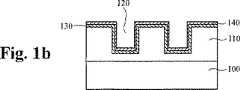
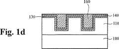
本発明による触媒を使用した銅CVDを簡略に説明すれば次の通りである。図1aを参照すれば、トレンチ120が基板100上部の絶縁膜110中に形成される。図1bで、導電性物質が絶縁膜110及び基板100に浸透することを防止するバリヤー膜130が基板の最上部に先に形成される。次に、銅シード層140がバリヤー膜130の上部に形成される。次の段階は図1cに示されたように触媒150を加えることである。最後に、図1dに示されたように銅CVDによって銅物質が蒸着される。
【0020】
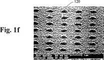
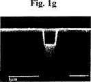
図1eは、銅で充填されたビアホール列の断面を示すSEM写真である。図1eはトレンチ中の銅層に比べて最上面の銅層が薄いことを示す。図1fは銅で充填されたビアホールアレイの上面を傾いた角度で撮ったSEM写真である。図1gは銅が部分的に充填されたビアホールの断面を示すSEM写真であって、銅がビアホールの底部から上部に充填されることを示す。図1hは銅が部分的に充填されたトレンチの断面を示すSEM写真であって、銅がトレンチの底部から上部に充填されることを示す。
【0021】
配線導電体を形成するために本発明により触媒を使用した銅CVDを使用すれば次のような長所がある。まず、本発明による銅充填方法は多層の配線導電体を形成するのに非常に適している。なぜなら前述した方法がトレンチ、ビアホール及びコンタクトをピンチ−オフやボイドなしに充填するからである。第2に、前述した銅充填方法はトレンチ、ビアホール及びコンタクトを充填し、扁平な表面には銅層を徐々に形成して高い銅原料を少なく消耗し、後続工程のためにCMPで除去されねばならない物質を減らす長所がある。第3に、触媒を使用したCVDで前述したCMP工程時間がはるかに短くなる。最上面の銅膜の厚さが非常に薄いからである。これにより、前述した銅充填方法は電気メッキのような従来の方法に比べて経済的である。
【0022】
本発明は後述する詳細な例示的で望ましい実施例を参照してよく理解できる。半導体素子を製造するにおいて、配線導電体を形成するために触媒を使用した銅CVDで配線導電体を形成するいくつかの例示的な方法が本発明によって開示されて提供される。当業者であれば本発明の範囲を外れずに配線導電体を形成する他の手段を容易に考えうる。したがって本発明による方法の範ちゅうはここに提供される望ましい実施例に限定されない。
【0023】
<第1実施例>
触媒を使用した銅CVD方法でトレンチ、ビアホール及びコンタクトのような配線導電体を形成する方法が後述される。
【0024】
最初の段階はサンプルを備えることである。図1aはシリコン基板100または絶縁膜110中のホール120をエッチングしたダマシン構造を示す。これは典型的なダマシン構造である。ホール120の最上端開口部の大きさはその幅が500nmであり、縦横比は2:1である(したがって、ホール120の深さは1,000nmである)。図1bを参照すれば、ホール120を含む全面にタンタル窒化膜TaN 130がスパッタリングで被覆される。このタンタル窒化膜は導電性物質140を蒸着する間に絶縁膜110に浸透することを防止するバリヤー膜である。そうしなければ、このような浸透は半導体−絶縁体関係の基本的な保全性を変更することによって、配線導電体を形成する目的を挫折させる。バリヤー膜として適した他の物質はTa、Ti、TiN、Ta−Si−N及びTi−Si−Nである。いくつかの絶縁膜は銅の浸透を阻止する性質があって、このような絶縁物質は銅に対するバリヤー膜として作用すると知られている。図1bを参照すれば、バリヤー膜130の上部に銅シード層140がスパッタリングで形成される。シード層の厚さは絶縁膜110の上部で30nmと測定され、ホールの内壁では約3nmと測定された。最も望ましいモード数値は絶縁膜110の上部で測定された約30nmである。
【0025】
図1cを参照すれば、5Torr真空で特殊制作した反応チャバを利用して前述したように備えられたサンプルを触媒150のヨード化エチルで処理する。後続的に、図1dに示したように、ホールが銅160で充填されるように、シリコン基板サンプルを銅原料物質(hfac)Cu(vtms)で3分間180℃、5Torr全体圧力のうち銅原料物質(hfac)Cu(vtms)分圧0.7Torr下でアルゴン運搬ガスと共に処理する。ここで、リガンド(hfac)はhexaフルオロアセチルアセトネートを意味し、リガンド(vtms)はビニールトリメチルシランを意味する。これにより図1eないし図1hのSEM写真を得る。
【0026】
図1eはピンチ−オフとボイドなしに均一に充填されたホールの断面を示す。図1fは完全に充填されたホールの上面を示す。図1gは充填段階初期に得たSEM写真であって、ホールの底部から上部に充填されることを示す。図1hもトレンチの底部から上部に銅が充填されることを示すSEM写真である。
【0027】
図1g及び図1hで分かるように、銅層はトレンチとホールの底部で速く成長し、トレンチ及びホールの最上部と内部でボイドピンチ−オフなしに上部側に成長する。銅層がトレンチ及びホール外側で100nmだけ成長しても、トレンチ及びホールの上部と内部にピンチ−オフやボイドが発生しないことを確認した。
【0028】
<第2実施例>
シリコン基板に埋め込まれた配線導電体は多様な形と大きさを有する。電力及び信号適用のための配線導電体は一般に大きい。しかし、前記の第1実施例で説明したような本発明による触媒を使用した銅CVDに基づいた銅充填方法は、入力/出力(I/O)信号及び電力線のためのパッドのように非常に小さな縦横比の広い面積を充填するには適していない。
【0029】
アルミニウム合金のような他の“柔らかい”金属とは異なって銅をエッチングすることが難しいために、本発明による銅蒸着方法と共にダマシン構造が使われねばならず、本発明による銅充填方法を使用するためには小さな縦横比を有する大きいトレンチが形成されねばならない。
【0030】
図1iを参照すれば、絶縁膜190中に大きいトレンチ192が形成されている。しかし、本発明による銅充填方法はこのような過度に大きいトレンチの充填に適していない。図1jに示したパターンは本発明による銅充填方法で伝導性“パッド”を形成するために、前記の第1実施例で説明された銅充填方法を活用する例である。一方、連続的な導電層を形成するのにいくつかの狭いトレンチが必要である。前記の全体トレンチ領域を充填しすぎれば良好な導電性“パッド”が提供される。図1jを参照すれば、全体トレンチ領域190中に多くの柱194と壁196がある。これにより多くの狭いトレンチ198が提供される。このような構造は信号I/O端子及び電力線のための伝導性“パッド”を形成するために、前記第1実施例で説明された本発明による銅充填方法を活用するより適当である。
【0031】
<第3実施例>
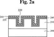
第1実施例で既に説明したように、図2aを参照すれば、最上面だけでなくトレンチ220内部にバリヤー膜230とシード層240を有するシリコン基板サンプルが備えられる。一般に、スパッタリング方法がシード層240だけでなくバリヤー膜230を形成するのに利用される。しかし、トレンチ及びビアホールの上端開口部が狭い場合にはTaNまたはTiNを使用してバリヤー膜230を形成するのにCVD方法が利用されることがあり、またシード層240を形成するのに触媒としてヨード化エチルを使用する銅CVD方法も利用されうる。銅原料物質(hfac)Cu(vtms)は第1実施例と同様にここに再び使われる。
【0032】
触媒ヨード化エチルは、図1cに示したように触媒を使用した銅CVDによって追加的な銅層260を形成する時にも加わりうるが、2次銅層260は電気メッキするための電極として使われるのに十分な厚さ(100nm以下)で形成する。電気メッキで完全に充填された銅層270が図2bに示される。
【0033】
この例示的な実施例は多少広いトレンチ、ビアホール及びコンタクトを充填する経済的な方法である。触媒を使用した銅CVDに使われる銅原料物質が電気メッキに使われる銅原料物質よりはるかに高いからである。
【0034】
<第4実施例>
一般に、二重ダマシン構造に電気メッキを使用することは難しいが、これは図3aでスタックされたトレンチ324で表現されたようにビアホールとスタックされたトレンチが深いからである。本発明による触媒を使用した銅充填方法はこのような二重ダマシン構造の状況でより適した方法である。
【0035】
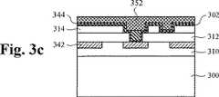
図3aを参照すれば、導電層342が基板300上面の第1絶縁膜310上にパターニングされている。導電体パターン342を有する第1絶縁膜310を通常の方法で平坦化した後、第2絶縁膜312が第1絶縁膜310上に蒸着され、コンタクトホール322が第2絶縁膜312内にエッチングされる。第3絶縁膜314を形成した後、トレンチ324がエッチングされる。結果的に、トレンチ324とコンタクトホール322とを含む二重ダマシン構造が形成される。次に、図3bを参照すれば、後続工程中に伝導性物質が絶縁膜に浸透することを防止するバリヤー膜302を全面に被覆した後、トレンチ324とコンタクトホール322とを充填するために銅シード層344がヨード化エチルを触媒として使用する銅CVD方法で形成される。シード層344の成長周期中にコンタクトホール322は図3bに示したように銅で充填される。一般に、ホールはトレンチより非常に速く銅で充填されるために、触媒を使用した銅CVD方法でホールは既に充填されたが、まだ充填が終わってないトレンチを充填するのには電気メッキ技術が利用されうる。後続的に、トレンチ324は図3cのように銅層352を電気メッキすることによって充填される。銅シード層344は銅シード層344が電気メッキの電極として使われうるほど厚くせねばならない(望ましくは100nm以下)。
【0036】
本発明によれば、ピンチ−オフとボイド発生なしにトレンチ、ビアホール及びコンタクトを銅で充填する。
【0037】
<第5実施例>
回路密度が増加するにつれてデザインルールは益々厳しくなり、トレンチとホールの上端開口部は益々狭くなって小さくなる。このような場合に、触媒は底部に深く浸透できなくて従来のスパッタリング方法は銅シード層を形成するのに適していない。したがって“触媒を加えてから銅を蒸着する”サイクルを反復的に行う必要がある。本実施例ではこのような場合の解決法を提示する。
【0038】
図4を参照すれば、第1実施例で説明されたように、シリコン基板410上の絶縁膜420中にトレンチまたはホールを形成した後、TiNまたはTaNを使用してバリヤー膜430を形成する。銅シード層440を形成するために、銅シード層の厚さが70nmを超えない(扁平な上面で測定した時)まで“触媒を加えてから銅を蒸着する”サイクルを少なくとも2回連続して反復的に行う。後続的に、前述した方法で形成された銅シード層が2次銅層450を形成するための電気メッキの電極として使われうる。
【0039】
本発明によれば、ピンチ−オフとボイドのない銅層450を、第1銅シード層440を電極として使用する電気メッキ方法で製造する。
【0040】
最後に、図4の導電体の扁平な上面を、後続工程で銅配線導電体を形成する段階を行うために必ず除去せねばならない。
【0041】
<第6実施例>
本発明によれば、触媒を使用した銅CVDで配線導電体を形成する方法は既に言及したように多くの長所を有する。まず、銅層成長速度はトレンチ、ビアホール及びコンタクトのように狭くて深い構造の底部で最も速い。順次に銅層が成長するにつれて成長速度は急激に減少し、一般に上面で最も遅くなる。結果的に、例えば図5aを参照すれば、トレンチ520は銅で速く充填されるが、上面には銅層554が一般に遅く成長して薄い銅層554だけ形成される。後続の段階で、良好な配線導電体を形成するために、導電層530、540、554は導電体の次の層が積もるように除去されねばならない。
【0042】
図5bは、本発明によって図5aの上部導電層530、540、554を従来のCMP方法で除去して平坦化する方法を示す。
【0043】
<第7実施例>
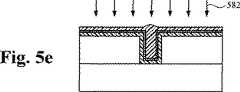
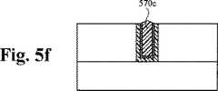
これは本発明によって図5aの上部導電層530、540、554をCMP方法で除去して平坦化する他の例示的方法である。図5cを参照すれば、化学エッチング剤580が銅層554の全面に加わって、図5dに示したように導電層のない扁平な表面が形成される。これは本発明により図5aの上面導電層530、540、554が非常に薄いために可能である。
【0044】
<第8実施例>
これは本発明によって図5aの上面導電層530、540、554を高温プラズマエッチングで除去して平坦化するさらに他の例示的方法である。図5eを参照すれば、高温プラズマエッチング582が図5aの上面導電層530、540、554を除去するために全面に加えられる。その結果、図5fの平坦な表面を得られる。これは本発明によって図5aの上面の導電層530、540、554が非常に薄いために可能である。
【0045】
<第9実施例>
これは本発明によって図5aの上面の導電層530、540、554を選択的エッチングで除去して平坦化するさらに他の例示的方法である。図5gを参照すれば、フォトレジストバリヤー膜584が必要に応じて形成される。次に残っている部分がエッチングされて、表面に導電体が残っていない扁平な上面だけでなく“突出した”導電体570dが形成される。これは本発明によって図5aの上面導電層530、540、554が非常に薄いために可能である。この“突出した”導電体570dは、例えばI/O端子のパッドとして使われうる。
【0046】
以上、本発明を望ましい実施例をあげて詳細に説明した。当業者であれば、本発明の範囲を外れずに配線導電体を形成する他の手段を容易に考えられる。したがって、本発明による方法の範ちゅうはここに提供される望ましい実施例に限定されない。
【0047】
【産業上の利用可能性】
配線導電体を形成するために本発明によって触媒を使用した銅CVDを使用することは次のような長所がある。まず、本発明による銅充填方法は多層の配線導電体を形成するのに適している。なぜなら前記の方法がトレンチ、ビアホール及びコンタクトをピンチ−オフやボイドなしに充填するからである。第2に、前述した銅充填方法はトレンチ、ビアホール及びコンタクトを速く充填し、扁平な表面には銅層を徐々に形成して高い銅原料を少なく消耗し、後続工程のためにCMPで除去されねばならない物質を減らす長所がある。第3に、触媒を使用したCVDで前述したCMP工程時間がはるかに短くなる。最上面の銅膜の厚さが非常に薄いからである。これにより、前述した銅充填方法は電気メッキのような従来の方法に比べて非常に経済的である。
【図面の簡単な説明】
【図1a】 銅物質で充填されたトレンチを形成する段階を示す一連の断面図である。
【図1b】 銅物質で充填されたトレンチを形成する段階を示す一連の断面図である。
【図1c】 銅物質で充填されたトレンチを形成する段階を示す一連の断面図である。
【図1d】 銅物質で充填されたトレンチを形成する段階を示す一連の断面図である。
【図1e】 銅で充填されたビアホール列の断面を示す走査電子顕微鏡(SEM)写真である。
【図1f】 銅で充填されたビアホールアレイの上面を傾いた角度で撮ったSEM写真である。
【図1g】 銅が部分的に充填されたビアホールの断面を示すSEM写真であって、銅がビアホールの底部から上部に充填されることを示す写真である。
【図1h】 銅が部分的に充填されたトレンチの断面を示すSEM写真であって、銅がトレンチの底部から上部に充填されることを示す写真である。
【図1i】 銅充填のために備えられた広いエッチング領域を示す図面である。
【図1j】 銅充填の向上のための壁と柱の例示パターンよりなる広いエッチング領域を示す図面である。
【図2a】 トレンチとビアホールを完全に充填するための従来の電気メッキのために十分に厚い2次銅層を示す例示断面図である。
【図2b】 銅で完全に充填されたトレンチを示す例示断面図である。
【図3a】 二重ダマシントレンチ−ビアホール構造のための一連の銅充填工程である。
【図3b】 二重ダマシントレンチ−ビアホール構造のための一連の銅充填工程である。
【図3c】 二重ダマシントレンチ−ビアホール構造のための一連の銅充填工程である。
【図4】 銅で薄膜を形成することを示す断面図である。
【図5a】 前記の図1dと類似であるが、銅がやや過度充填されたトレンチの断面図である。
【図5b】 トレンチ内部に配線導電体を形成するためにCMP方法で図5aの表面層を除去した結果を示す断面図である。
【図5c】 上部の化学エッチング剤を示す図5aの断面図である。
【図5d】 トレンチ配線導電体を形成するために上部層がエッチングされた後の図5cの断面図である。
【図5e】 プラズマエッチング工程を示す図5aの断面図である。
【図5f】 トレンチ内部に配線導電体を形成するために上部銅層をプラズマエッチングした後の図5eの断面図である。
【図5g】 上部のフォトレジスト層を示す図5aの断面図である。
【図5h】 上部銅層とエッチングにより選択的に除去されたフォトレジストを含む図5gの断面図である。[0001]
【Technical field】
The present invention relates to a method for forming a copper-based wiring such as a trench, a via hole, a contact, and a thin film by chemical vapor deposition (CVD) using a catalyst at a submicron level in a semiconductor technology area.
[0002]
[Background]
In addition to providing signal and power lines, interconnecting active and passive devices plays an important role in the production process of semiconductor related products.
[0003]
The most widely used method is a method of using an aluminum-based metal by vapor deposition, etching, or the like. This is because aluminum alloys are relatively easy and cheap to manufacture and obtain. However, aluminum alloys are vulnerable to thermal stresses and high electrical stresses, leading to damage known as electromigration problems mainly due to particle size.
[0004]
In addition, as element design rules become more stringent, the particle size of aluminum alloys is receiving more attention due to the electromigration-related problems described above. Aluminum alloys are generally known as good conductors and satisfy wiring requirements including electrical performance requirements such as RC time delay.
[0005]
With the recent rapid increase in circuit density, there are fewer electromigration problems, making high performance devices more desirable in terms of not only the strong physical properties of wiring conductors but also short delays and better electrical conductivity. As a result, research to replace aluminum alloys with better conductive materials, particularly copper materials, has become active.
[0006]
Copper has the advantage of having high electrical conductivity, among which copper can carry more current while being less electromigration-problem and is stiffer than aluminum. On the other hand, because it is harder than aluminum, the “post-deposition-etching process” is more difficult than the etching of aluminum alloys that are applied immediately. Therefore, for example, a damascene process is used to form the wiring conductor. Here, the trench is formed on the insulating film by etching and then filled with copper. In addition, via holes or contact holes are used to connect two conductors in two different layers, one located on top of the other. In such a case, a double damascene process can be used, but here once after the two-step process of forming via holes or contact holes and trenches in two adjacent layers, one on top of the other. In the process, the via hole or contact hole and the trench are filled with copper.
[0007]
As a known technique for filling the trench and the hole, there is an electroplating (EP) method. However, this process is not very suitable for the conventional semiconductor manufacturing process. Also, this process is somewhat complicated and needs to be further developed to achieve high yields in a mass production environment. The use of physical vapor deposition (PVD), such as chemical vapor deposition (CVD) or sputtering, is desirable to meet conventional semiconductor device manufacturing processes. When using sputtering techniques to form wiring conductors using trenches and holes, a pinch-off phenomenon occurs near the top opening of the deep trench or deep hole. In other words, the upper end of the opening is blocked before the remaining portion of the trench or hole is filled. This is due to the unique nature of “straight forward” deposition along the “line of sight” that commonly occurs during PVD processes. This is the reason why sputtering is not suitable for the production of submicron class semiconductor devices.
[0008]
On the other hand, the use of CVD methods is known to nucleate and allow growth of thin films. The CVD method is known to have excellent step coverage, and the deposited film or thin film covers not only corners but also flat portions (flat portions at the top and bottom) and side walls. However, when the substrate temperature is about 200 ° C. and the copper material is deposited by CVD, the film growth rate drops to 50 nm / min or less, which is not only regarded as a slow rate but also like an island at the beginning of growth after thin film nucleation. It has been reported that unevenness of the film surface occurs due to growth.
[0009]
In order to solve the above-mentioned problems of a considerably low growth rate of the thin film and unevenness of the thin film surface when the CVD method is used for thin film formation, a chemical vapor deposition method utilizing a catalyst on the surface is disclosed in US application 09 / lee by Lee. Proposed in 554,444. The chemical vapor deposition method proposed here proposes using iodine or bromine belonging to the halogen element group together with CVD as a catalyst. This method not only significantly increases the growth rate of the copper film, but also reduces the resulting film surface irregularities.
[0010]
As will be described later, the present invention proposes a method of forming copper wiring conductors such as trenches, via holes, contacts, and thin films by CVD using a catalyst.
[0011]
DISCLOSURE OF THE INVENTION
As a copper CVD method using a catalyst, a method of forming a copper wiring conductor by filling a trench, a via hole and a contact without occurrence of pinch-off or void is disclosed and provided.
[0012]
In a first aspect of the present invention, there is disclosed and provided a method for filling trenches, via holes and contacts without the use of undesired pinch-offs or voids using iodine or bromine as a catalyst with a copper CVD method. This method fills the bottom of the trench and hole very quickly without pinch-off or voids, and the deposition rate decreases as the trench or hole fills from bottom to top, with copper at the lowest speed at the top. Vapor deposited. Unlike conventional methods such as the PVD method, copper CVD using a catalyst does not pinch-off at the top opening of the trench and hole.
[0013]
In a second aspect of the present invention, a method for forming a copper layer by repeatedly applying the method described in the first aspect of the present invention in a narrow and deep trench and a small and deep hole is disclosed and provided. This method allows copper material only in the trench and hole depth, and deep trenches and holes are filled with copper. On the other hand, conventional methods such as sputtering techniques do not allow such deep penetration.
[0014]
In a third aspect of the present invention, a method for forming a very thin copper layer on the top surface is disclosed and provided. This allows the thin copper layer to be removed by an etch back means in preparation for the next process step, but such removal is usually done by a high cost CMP method. Typically, common electroplating techniques also require CMP to remove the copper formed on the top surface in preparation for the next process step.
[0015]
The invention, together with embodiments and advantages thereof, may best be understood by referring to the detailed description of embodiments described below in conjunction with the accompanying drawings.
[0016]
BEST MODE FOR CARRYING OUT THE INVENTION
In accordance with the present invention, a copper wiring conductor in a copper CVD process using a catalyst to interconnect active and passive elements as well as circuit signal and power lines, as well as elements and other elements on a silicon wafer. A method of forming is disclosed and provided. More particularly, a method for filling trenches, via holes and contacts for wiring is disclosed and provided. According to another aspect of the present invention, a method for filling power elements, power line holes and wide trenches as well as wide passive elements is disclosed and provided herein. According to another aspect of the present invention, a method for filling a narrow and deep trench and a small depression such as a small diameter and deep hole with copper CVD using a catalyst, which cannot use a conventional method such as electroplating, is also disclosed. Is done. This method can later be used as a means for depositing a seed layer for electroplating the remainder of the depression for economic reasons. Another object aspect of the present invention provides a method for forming a very thin film layer on a flat top of a wafer surface in addition to the formation of a copper wiring conductor. Thereby, the flat top thin film can be removed by wet or dry etch back or high temperature plasma etch back process in preparation for the next process step. This eliminates the need to use very high CMP methods.
[0017]
According to the present invention, the use of copper CVD using a catalyst allows the deposition of copper from the bottom to the top, and, for example, pinch-off at the top opening of the trench and voids inside the trench Without filling the trench. In addition, according to the present invention, because of the high deposition rate at the bottom of the trench and slow at the flat top between the two trenches and the sidewalls of the trench, the catalyst-enhanced copper CVD can connect the trench, via hole and contact to the copper. It is an ideal process of filling with. In particular, the deposition rate on the flat top is the slowest, but the copper CVD using a catalyst deposits a thin copper layer on the flat surface because the deposition rate of copper thin film is faster than other conventional methods. An excellent way to do it. However, the deposition rate decreases rapidly as the film thickness increases. In order to form a thicker film, it is necessary to repeat the “catalyst followed by copper deposition” cycle, which is an aspect of the invention disclosed herein.
[0018]
Referring to FIG. 1c, there are two inferences after the phenomenon of “filling the bottom first and then depositing quickly”. First, in FIG. 1c, the catalyst acts as a good surfactant and the copper atoms travel around the periphery very quickly on the surface of the copper seed layer. As the copper layer builds up on the seed layer, the copper film grows in such a way that the growing surface area is minimized in a limited space in the trench or hole. Another reason is that as the copper film grows, the surface area decreases, thereby increasing the “density” of the catalyst. This increases the copper growth rate and the deposition rate is faster than outside the trench or hole. The growth rate is generally the fastest at the bottom of the trench or hole because the surface area reduction rate is generally the fastest at the bottom of the trench or hole. For the same reason, the corners at the bottom of the trench or hole are filled first. Here, as will be understood from the detailed description to be described later, a preferable catalyst is a halogen element group, more specifically, iodine and bromine.
[0019]
The copper CVD using the catalyst according to the present invention will be briefly described as follows. Referring to FIG. 1 a, a
[0020]
FIG. 1e is a SEM photograph showing a cross-section of a via hole array filled with copper. FIG. 1e shows that the uppermost copper layer is thinner than the copper layer in the trench. FIG. 1f is an SEM photograph taken at an inclined angle of the top surface of the via hole array filled with copper. FIG. 1g is a SEM photograph showing a cross-section of a via hole partially filled with copper, showing that copper is filled from the bottom to the top of the via hole. FIG. 1h is a SEM photograph showing a cross-section of a trench partially filled with copper, showing that copper is filled from the bottom to the top of the trench.
[0021]
The use of copper CVD using a catalyst according to the present invention to form a wiring conductor has the following advantages. First, the copper filling method according to the present invention is very suitable for forming a multilayer wiring conductor. This is because the above-described method fills trenches, via holes and contacts without pinch-off or voids. Second, the copper filling method described above fills trenches, via holes, and contacts, and gradually forms a copper layer on a flat surface to consume less high copper material and must be removed by CMP for subsequent processes. There is an advantage to reduce the material that should not be. Third, the CMP process time described above in the CVD using a catalyst is much shorter. This is because the uppermost copper film is very thin. As a result, the copper filling method described above is more economical than conventional methods such as electroplating.
[0022]
The invention may be better understood with reference to the following detailed exemplary preferred embodiments. Several exemplary methods of forming wiring conductors by copper CVD using a catalyst to form wiring conductors in the manufacture of semiconductor devices are disclosed and provided by the present invention. Those skilled in the art can easily conceive other means for forming the wiring conductor without departing from the scope of the present invention. Accordingly, the scope of the method according to the present invention is not limited to the preferred embodiments provided herein.
[0023]
<First embodiment>
A method of forming wiring conductors such as trenches, via holes, and contacts by a copper CVD method using a catalyst will be described later.
[0024]
The first step is to provide a sample. FIG. 1 a shows a damascene structure in which holes 120 in the
[0025]
Referring to FIG. 1 c, a sample prepared as described above is treated with ethyl iodide of catalyst 150 using a reaction chamber specifically produced in a 5 Torr vacuum. Subsequently, as shown in FIG. 1 d, the silicon substrate sample is made of copper source material (hfac) Cu (vtms) for 3 minutes at 180 ° C. and 5 Torr total pressure so that the holes are filled with
[0026]
FIG. 1e shows a cross-section of a uniformly filled hole without pinch-off and voids. FIG. 1f shows the top surface of the fully filled hole. FIG. 1g is an SEM photograph obtained early in the filling stage, showing that the hole is filled from the bottom to the top. FIG. 1h is also a SEM photograph showing that the trench is filled from the bottom to the top.
[0027]
As can be seen in FIGS. 1g and 1h, the copper layer grows fast at the bottom of the trench and hole and grows to the top without void pinch-off at the top and inside of the trench and hole. It was confirmed that no pinch-off or void was generated in the upper part and inside of the trench and hole even when the copper layer was grown by 100 nm outside the trench and hole.
[0028]
<Second embodiment>
The wiring conductor embedded in the silicon substrate has various shapes and sizes. Wiring conductors for power and signal applications are generally large. However, the copper filling method based on copper CVD using the catalyst according to the present invention as described in the first embodiment is very much like a pad for input / output (I / O) signals and power lines. Not suitable for filling large areas with small aspect ratios.
[0029]
Because it is difficult to etch copper unlike other “soft” metals such as aluminum alloys, a damascene structure must be used with the copper deposition method of the present invention, and the copper filling method of the present invention is used. In order to do this, a large trench having a small aspect ratio must be formed.
[0030]
Referring to FIG. 1 i, a
[0031]
<Third embodiment>
As already described in the first embodiment, referring to FIG. 2A, a silicon substrate sample having a
[0032]
Catalytic ethyl iodide can also be added when forming an
[0033]
This exemplary embodiment is an economical way to fill somewhat wider trenches, via holes and contacts. This is because the copper raw material used for copper CVD using a catalyst is much higher than the copper raw material used for electroplating.
[0034]
<Fourth embodiment>
In general, it is difficult to use electroplating for a double damascene structure because the trenches stacked with via holes are deep as represented by the
[0035]
Referring to FIG. 3 a, a
[0036]
According to the present invention, the trench, via hole and contact are filled with copper without pinch-off and void generation.
[0037]
<Fifth embodiment>
As circuit density increases, the design rules become stricter and the top openings of the trenches and holes become narrower and smaller. In such a case, the catalyst cannot penetrate deeply into the bottom and conventional sputtering methods are not suitable for forming a copper seed layer. Therefore, it is necessary to repeatedly perform the cycle of “deposition of copper after adding catalyst”. In this embodiment, a solution for such a case is presented.
[0038]
Referring to FIG. 4, after the trench or hole is formed in the insulating
[0039]
In accordance with the present invention, pinch-off and void-
[0040]
Finally, the flat top surface of the conductor of FIG. 4 must be removed in order to perform a step of forming a copper wiring conductor in a subsequent process.
[0041]
<Sixth embodiment>
According to the present invention, the method of forming a wiring conductor by copper CVD using a catalyst has many advantages as already mentioned. First, the growth rate of the copper layer is the fastest at the bottom of a narrow and deep structure such as a trench, a via hole and a contact. As the copper layer grows sequentially, the growth rate decreases rapidly and is generally slowest on the top surface. As a result, referring to FIG. 5a, for example, the
[0042]
FIG. 5b illustrates a method of removing and planarizing the upper
[0043]
<Seventh embodiment>
This is another exemplary method of removing and planarizing the upper
[0044]
<Eighth embodiment>
This is yet another exemplary method of removing and planarizing the top
[0045]
<Ninth embodiment>
This is yet another exemplary method for removing and planarizing the
[0046]
The present invention has been described in detail with reference to the preferred embodiments. A person skilled in the art can easily conceive other means of forming the wiring conductor without departing from the scope of the present invention. Accordingly, the scope of the method according to the present invention is not limited to the preferred embodiments provided herein.
[0047]
[Industrial applicability]
The use of copper CVD using a catalyst according to the present invention to form a wiring conductor has the following advantages. First, the copper filling method according to the present invention is suitable for forming a multilayer wiring conductor. This is because the above method fills trenches, via holes and contacts without pinch-off or voids. Second, the copper filling method described above fills trenches, via holes, and contacts quickly, and gradually forms a copper layer on a flat surface to consume less high copper material and is removed by CMP for subsequent processes. There is an advantage to reduce the material that must be. Third, the CMP process time described above in the CVD using a catalyst is much shorter. This is because the uppermost copper film is very thin. As a result, the copper filling method described above is much more economical than conventional methods such as electroplating.
[Brief description of the drawings]
FIG. 1a is a series of cross-sectional views illustrating the steps of forming a trench filled with a copper material.
FIG. 1b is a series of cross-sectional views illustrating the steps of forming a trench filled with copper material.
FIG. 1c is a series of cross-sectional views illustrating the steps of forming a trench filled with a copper material.
FIG. 1d is a series of cross-sectional views illustrating the steps of forming a trench filled with copper material.
FIG. 1e is a scanning electron microscope (SEM) photograph showing a cross section of a via hole array filled with copper.
FIG. 1f is an SEM photograph taken at an angle of the top surface of a via hole array filled with copper.
FIG. 1g is a SEM photograph showing a cross-section of a via hole partially filled with copper, showing that copper is filled from the bottom to the top of the via hole.
FIG. 1h is a SEM photograph showing a cross-section of a trench partially filled with copper, showing copper filling from the bottom to the top of the trench.
FIG. 1i shows a large etching area provided for copper filling.
FIG. 1j is a drawing showing a wide etched area of exemplary patterns of walls and pillars for improved copper filling.
FIG. 2a is an exemplary cross-sectional view showing a secondary copper layer that is sufficiently thick for conventional electroplating to completely fill trenches and via holes.
FIG. 2b is an exemplary cross-sectional view showing a trench completely filled with copper.
FIG. 3a is a series of copper filling steps for a double damascene trench-via hole structure.
FIG. 3b is a series of copper filling steps for a double damascene trench-via hole structure.
FIG. 3c is a series of copper filling steps for a double damascene trench-via hole structure.
FIG. 4 is a cross-sectional view showing that a thin film is formed from copper.
FIG. 5a is a cross-sectional view of a trench similar to FIG. 1d above, but slightly overfilled with copper.
FIG. 5b is a cross-sectional view showing a result of removing the surface layer of FIG. 5a by a CMP method in order to form a wiring conductor inside the trench.
FIG. 5c is a cross-sectional view of FIG. 5a showing the upper chemical etchant.
FIG. 5d is a cross-sectional view of FIG. 5c after the top layer has been etched to form a trench interconnect conductor.
FIG. 5e is a cross-sectional view of FIG. 5a showing the plasma etching process.
FIG. 5f is a cross-sectional view of FIG. 5e after plasma etching the upper copper layer to form a wiring conductor within the trench.
FIG. 5g is a cross-sectional view of FIG. 5a showing the upper photoresist layer.
FIG. 5h is a cross-sectional view of FIG. 5g including the upper copper layer and the photoresist selectively removed by etching.
Claims (10)
Translated fromJapanese前記陥没部が形成された絶縁膜上にシード層を形成する段階、
前記シード層に触媒を加える段階、及び
前記触媒が加えられたシード層上に化学気相蒸着によって銅層を形成する段階を含み、
前記触媒はヨード又はブロムを含む配線導電体の形成方法。Forming a depression in one or more insulating films formed on the silicon substrate;
Forming a seed layer on the insulating film in which the depression is formed;
Adding a catalyst to the seed layer; and forming a copper layer by chemical vapor deposition on the seed layer to which the catalyst is added.
A method of forming a wiring conductor in which the catalyst contains iodine or bromine.
Applications Claiming Priority (9)
| Application Number | Priority Date | Filing Date | Title |
|---|---|---|---|
| KR1999/57939 | 1999-12-15 | ||
| KR19990057939 | 1999-12-15 | ||
| KR1999/59862 | 1999-12-21 | ||
| KR1019990059862AKR20010063028A (en) | 1999-12-21 | 1999-12-21 | Method for forming copper interconnects |
| KR1019990061129AKR20010057734A (en) | 1999-12-23 | 1999-12-23 | Method of forming a copper thin film |
| KR1999/61129 | 1999-12-23 | ||
| KR1020000001232AKR20010066720A (en) | 1999-12-15 | 2000-01-11 | Method of forming Copper interconnects |
| KR2000/1232 | 2000-01-11 | ||
| PCT/KR2000/001474WO2001045149A1 (en) | 1999-12-15 | 2000-12-15 | Method of forming copper interconnections and thin films using chemical vapor deposition with catalyst |
Related Child Applications (2)
| Application Number | Title | Priority Date | Filing Date |
|---|---|---|---|
| JP2006336416ADivisionJP4792379B2 (en) | 1999-12-15 | 2006-12-13 | Method for forming copper wiring and thin film using catalyst and chemical vapor deposition |
| JP2006336417ADivisionJP2007123924A (en) | 1999-12-15 | 2006-12-13 | Method of forming copper interconnection and thin film using catalyst and chemical vapor deposition method |
Publications (2)
| Publication Number | Publication Date |
|---|---|
| JP2003517205A JP2003517205A (en) | 2003-05-20 |
| JP3925780B2true JP3925780B2 (en) | 2007-06-06 |
Family
ID=27483406
Family Applications (3)
| Application Number | Title | Priority Date | Filing Date |
|---|---|---|---|
| JP2001545352AExpired - LifetimeJP3925780B2 (en) | 1999-12-15 | 2000-12-15 | Method for forming copper wiring and thin film using catalyst and chemical vapor deposition |
| JP2006336417APendingJP2007123924A (en) | 1999-12-15 | 2006-12-13 | Method of forming copper interconnection and thin film using catalyst and chemical vapor deposition method |
| JP2006336416AExpired - LifetimeJP4792379B2 (en) | 1999-12-15 | 2006-12-13 | Method for forming copper wiring and thin film using catalyst and chemical vapor deposition |
Family Applications After (2)
| Application Number | Title | Priority Date | Filing Date |
|---|---|---|---|
| JP2006336417APendingJP2007123924A (en) | 1999-12-15 | 2006-12-13 | Method of forming copper interconnection and thin film using catalyst and chemical vapor deposition method |
| JP2006336416AExpired - LifetimeJP4792379B2 (en) | 1999-12-15 | 2006-12-13 | Method for forming copper wiring and thin film using catalyst and chemical vapor deposition |
Country Status (6)
| Country | Link |
|---|---|
| US (1) | US6720262B2 (en) |
| EP (1) | EP1247292B1 (en) |
| JP (3) | JP3925780B2 (en) |
| KR (1) | KR100465982B1 (en) |
| DE (1) | DE60041522D1 (en) |
| WO (1) | WO2001045149A1 (en) |
Families Citing this family (293)
| Publication number | Priority date | Publication date | Assignee | Title |
|---|---|---|---|---|
| US6727169B1 (en) | 1999-10-15 | 2004-04-27 | Asm International, N.V. | Method of making conformal lining layers for damascene metallization |
| WO2001078123A1 (en)* | 2000-04-11 | 2001-10-18 | Genitech Co., Ltd. | Method of forming metal interconnects |
| US7494927B2 (en)* | 2000-05-15 | 2009-02-24 | Asm International N.V. | Method of growing electrical conductors |
| KR100407679B1 (en)* | 2000-06-15 | 2003-12-01 | 주식회사 하이닉스반도체 | Method of forming a copper wiring in a semiconductor device |
| KR100407678B1 (en)* | 2000-06-15 | 2003-12-01 | 주식회사 하이닉스반도체 | Method of forming a copper metal wiring in a semiconductor device |
| KR100383759B1 (en)* | 2000-06-15 | 2003-05-14 | 주식회사 하이닉스반도체 | Method of forming a copper metal wiring in a semiconductor drvice |
| KR100671610B1 (en)* | 2000-10-26 | 2007-01-18 | 주식회사 하이닉스반도체 | Metal wiring formation method of semiconductor device |
| AU2002306436A1 (en) | 2001-02-12 | 2002-10-15 | Asm America, Inc. | Improved process for deposition of semiconductor films |
| JP3643807B2 (en)* | 2001-11-14 | 2005-04-27 | 三菱重工業株式会社 | Etching method and etching apparatus |
| KR100805843B1 (en)* | 2001-12-28 | 2008-02-21 | 에이에스엠지니텍코리아 주식회사 | Copper wiring forming method, semiconductor device and copper wiring forming system manufactured accordingly |
| US7186630B2 (en) | 2002-08-14 | 2007-03-06 | Asm America, Inc. | Deposition of amorphous silicon-containing films |
| US7084509B2 (en) | 2002-10-03 | 2006-08-01 | International Business Machines Corporation | Electronic package with filled blinds vias |
| KR100487639B1 (en)* | 2002-12-11 | 2005-05-03 | 주식회사 하이닉스반도체 | Method for forming metal line of semiconductor device |
| US20040248403A1 (en)* | 2003-06-09 | 2004-12-09 | Dubin Valery M. | Method for forming electroless metal low resistivity interconnects |
| US7816236B2 (en) | 2005-02-04 | 2010-10-19 | Asm America Inc. | Selective deposition of silicon-containing films |
| US8025922B2 (en)* | 2005-03-15 | 2011-09-27 | Asm International N.V. | Enhanced deposition of noble metals |
| US7608549B2 (en)* | 2005-03-15 | 2009-10-27 | Asm America, Inc. | Method of forming non-conformal layers |
| US7666773B2 (en) | 2005-03-15 | 2010-02-23 | Asm International N.V. | Selective deposition of noble metal thin films |
| US7999330B2 (en)* | 2005-06-24 | 2011-08-16 | Micron Technology, Inc. | Dynamic random access memory device and electronic systems |
| US20070014919A1 (en)* | 2005-07-15 | 2007-01-18 | Jani Hamalainen | Atomic layer deposition of noble metal oxides |
| US7365011B2 (en)* | 2005-11-07 | 2008-04-29 | Intel Corporation | Catalytic nucleation monolayer for metal seed layers |
| WO2007078802A2 (en) | 2005-12-22 | 2007-07-12 | Asm America, Inc. | Epitaxial deposition of doped semiconductor materials |
| KR101379015B1 (en) | 2006-02-15 | 2014-03-28 | 한국에이에스엠지니텍 주식회사 | METHOD OF DEPOSITING Ru FILM USING PEALD AND DENSE Ru FILM |
| CN101395290B (en)* | 2006-02-28 | 2010-11-10 | 合同会社先端配线材料研究所 | Semiconductor device, method for manufacturing the same, and sputtering target used for the manufacturing method |
| US7354849B2 (en)* | 2006-02-28 | 2008-04-08 | Intel Corporation | Catalytically enhanced atomic layer deposition process |
| US7701031B2 (en)* | 2006-04-07 | 2010-04-20 | United Microelectronics Corp. | Integrated circuit structure and manufacturing method thereof |
| US7993972B2 (en) | 2008-03-04 | 2011-08-09 | Stats Chippac, Ltd. | Wafer level die integration and method therefor |
| US8278176B2 (en) | 2006-06-07 | 2012-10-02 | Asm America, Inc. | Selective epitaxial formation of semiconductor films |
| US7694413B2 (en)* | 2006-06-30 | 2010-04-13 | Intel Corporation | Method of making a bottomless via |
| KR100895811B1 (en) | 2006-08-31 | 2009-05-06 | 주식회사 하이닉스반도체 | Metal wiring formation method of semiconductor device |
| US7435484B2 (en)* | 2006-09-01 | 2008-10-14 | Asm Japan K.K. | Ruthenium thin film-formed structure |
| US20080078983A1 (en)* | 2006-09-28 | 2008-04-03 | Wolfgang Raberg | Layer structures comprising chalcogenide materials |
| US20080124484A1 (en)* | 2006-11-08 | 2008-05-29 | Asm Japan K.K. | Method of forming ru film and metal wiring structure |
| KR20080074645A (en)* | 2007-02-09 | 2008-08-13 | 주식회사 하이닉스반도체 | Manufacturing method of semiconductor device |
| US20080242078A1 (en)* | 2007-03-30 | 2008-10-02 | Asm Nutool, Inc. | Process of filling deep vias for 3-d integration of substrates |
| US7632585B2 (en) | 2007-04-11 | 2009-12-15 | Eveready Battery Co., Inc. | Battery having fluid regulator with pressure equalization |
| US7618739B2 (en) | 2007-04-11 | 2009-11-17 | Eveready Battery Co., Inc. | Battery and fluid regulating system having chassis with molded electronics |
| US7759199B2 (en) | 2007-09-19 | 2010-07-20 | Asm America, Inc. | Stressor for engineered strain on channel |
| US20090087339A1 (en)* | 2007-09-28 | 2009-04-02 | Asm Japan K.K. | METHOD FOR FORMING RUTHENIUM COMPLEX FILM USING Beta-DIKETONE-COORDINATED RUTHENIUM PRECURSOR |
| KR101544198B1 (en) | 2007-10-17 | 2015-08-12 | 한국에이에스엠지니텍 주식회사 | Ruthenium film formation method |
| US7655564B2 (en)* | 2007-12-12 | 2010-02-02 | Asm Japan, K.K. | Method for forming Ta-Ru liner layer for Cu wiring |
| KR20090067505A (en)* | 2007-12-21 | 2009-06-25 | 에이에스엠지니텍코리아 주식회사 | Ruthenium film deposition method |
| US7655543B2 (en) | 2007-12-21 | 2010-02-02 | Asm America, Inc. | Separate injection of reactive species in selective formation of films |
| US7799674B2 (en)* | 2008-02-19 | 2010-09-21 | Asm Japan K.K. | Ruthenium alloy film for copper interconnects |
| US8084104B2 (en)* | 2008-08-29 | 2011-12-27 | Asm Japan K.K. | Atomic composition controlled ruthenium alloy film formed by plasma-enhanced atomic layer deposition |
| US8133555B2 (en) | 2008-10-14 | 2012-03-13 | Asm Japan K.K. | Method for forming metal film by ALD using beta-diketone metal complex |
| US9379011B2 (en) | 2008-12-19 | 2016-06-28 | Asm International N.V. | Methods for depositing nickel films and for making nickel silicide and nickel germanide |
| US8486191B2 (en) | 2009-04-07 | 2013-07-16 | Asm America, Inc. | Substrate reactor with adjustable injectors for mixing gases within reaction chamber |
| US20110020546A1 (en)* | 2009-05-15 | 2011-01-27 | Asm International N.V. | Low Temperature ALD of Noble Metals |
| US8329569B2 (en)* | 2009-07-31 | 2012-12-11 | Asm America, Inc. | Deposition of ruthenium or ruthenium dioxide |
| JP5788785B2 (en)* | 2011-01-27 | 2015-10-07 | 東京エレクトロン株式会社 | Cu wiring forming method and film forming system |
| JP5767570B2 (en)* | 2011-01-27 | 2015-08-19 | 東京エレクトロン株式会社 | Cu wiring forming method, Cu film forming method, and film forming system |
| US8658533B2 (en) | 2011-03-10 | 2014-02-25 | International Business Machines Corporation | Semiconductor interconnect structure with multi-layered seed layer providing enhanced reliability and minimizing electromigration |
| US8871617B2 (en) | 2011-04-22 | 2014-10-28 | Asm Ip Holding B.V. | Deposition and reduction of mixed metal oxide thin films |
| US8809170B2 (en) | 2011-05-19 | 2014-08-19 | Asm America Inc. | High throughput cyclical epitaxial deposition and etch process |
| US20130023129A1 (en) | 2011-07-20 | 2013-01-24 | Asm America, Inc. | Pressure transmitter for a semiconductor processing environment |
| US8648465B2 (en) | 2011-09-28 | 2014-02-11 | International Business Machines Corporation | Semiconductor interconnect structure having enhanced performance and reliability |
| CN103545196B (en)* | 2012-07-13 | 2017-04-19 | 中芯国际集成电路制造(上海)有限公司 | Manufacturing method of metal interconnecting wires |
| US20160376700A1 (en) | 2013-02-01 | 2016-12-29 | Asm Ip Holding B.V. | System for treatment of deposition reactor |
| CN103531446A (en)* | 2013-10-18 | 2014-01-22 | 上海华力微电子有限公司 | Method for preparing interconnected structure of metal hard mask layer and copper |
| US10941490B2 (en) | 2014-10-07 | 2021-03-09 | Asm Ip Holding B.V. | Multiple temperature range susceptor, assembly, reactor and system including the susceptor, and methods of using the same |
| US10276355B2 (en) | 2015-03-12 | 2019-04-30 | Asm Ip Holding B.V. | Multi-zone reactor, system including the reactor, and method of using the same |
| US9607842B1 (en) | 2015-10-02 | 2017-03-28 | Asm Ip Holding B.V. | Methods of forming metal silicides |
| US11139308B2 (en) | 2015-12-29 | 2021-10-05 | Asm Ip Holding B.V. | Atomic layer deposition of III-V compounds to form V-NAND devices |
| US10529554B2 (en) | 2016-02-19 | 2020-01-07 | Asm Ip Holding B.V. | Method for forming silicon nitride film selectively on sidewalls or flat surfaces of trenches |
| US10343920B2 (en) | 2016-03-18 | 2019-07-09 | Asm Ip Holding B.V. | Aligned carbon nanotubes |
| US11453943B2 (en) | 2016-05-25 | 2022-09-27 | Asm Ip Holding B.V. | Method for forming carbon-containing silicon/metal oxide or nitride film by ALD using silicon precursor and hydrocarbon precursor |
| US10612137B2 (en) | 2016-07-08 | 2020-04-07 | Asm Ip Holdings B.V. | Organic reactants for atomic layer deposition |
| US9859151B1 (en) | 2016-07-08 | 2018-01-02 | Asm Ip Holding B.V. | Selective film deposition method to form air gaps |
| US9812320B1 (en) | 2016-07-28 | 2017-11-07 | Asm Ip Holding B.V. | Method and apparatus for filling a gap |
| US9887082B1 (en) | 2016-07-28 | 2018-02-06 | Asm Ip Holding B.V. | Method and apparatus for filling a gap |
| US11532757B2 (en) | 2016-10-27 | 2022-12-20 | Asm Ip Holding B.V. | Deposition of charge trapping layers |
| US10714350B2 (en) | 2016-11-01 | 2020-07-14 | ASM IP Holdings, B.V. | Methods for forming a transition metal niobium nitride film on a substrate by atomic layer deposition and related semiconductor device structures |
| KR102546317B1 (en) | 2016-11-15 | 2023-06-21 | 에이에스엠 아이피 홀딩 비.브이. | Gas supply unit and substrate processing apparatus including the same |
| US11581186B2 (en) | 2016-12-15 | 2023-02-14 | Asm Ip Holding B.V. | Sequential infiltration synthesis apparatus |
| US11447861B2 (en) | 2016-12-15 | 2022-09-20 | Asm Ip Holding B.V. | Sequential infiltration synthesis apparatus and a method of forming a patterned structure |
| US11390950B2 (en) | 2017-01-10 | 2022-07-19 | Asm Ip Holding B.V. | Reactor system and method to reduce residue buildup during a film deposition process |
| US10468261B2 (en) | 2017-02-15 | 2019-11-05 | Asm Ip Holding B.V. | Methods for forming a metallic film on a substrate by cyclical deposition and related semiconductor device structures |
| KR102406573B1 (en) | 2017-04-28 | 2022-06-09 | 삼성전자주식회사 | Semiconductor device and method for manufacturing the same |
| US10770286B2 (en) | 2017-05-08 | 2020-09-08 | Asm Ip Holdings B.V. | Methods for selectively forming a silicon nitride film on a substrate and related semiconductor device structures |
| US12040200B2 (en) | 2017-06-20 | 2024-07-16 | Asm Ip Holding B.V. | Semiconductor processing apparatus and methods for calibrating a semiconductor processing apparatus |
| US11306395B2 (en) | 2017-06-28 | 2022-04-19 | Asm Ip Holding B.V. | Methods for depositing a transition metal nitride film on a substrate by atomic layer deposition and related deposition apparatus |
| KR20190009245A (en) | 2017-07-18 | 2019-01-28 | 에이에스엠 아이피 홀딩 비.브이. | Methods for forming a semiconductor device structure and related semiconductor device structures |
| US11374112B2 (en) | 2017-07-19 | 2022-06-28 | Asm Ip Holding B.V. | Method for depositing a group IV semiconductor and related semiconductor device structures |
| US10590535B2 (en) | 2017-07-26 | 2020-03-17 | Asm Ip Holdings B.V. | Chemical treatment, deposition and/or infiltration apparatus and method for using the same |
| TWI815813B (en) | 2017-08-04 | 2023-09-21 | 荷蘭商Asm智慧財產控股公司 | Showerhead assembly for distributing a gas within a reaction chamber |
| US10770336B2 (en) | 2017-08-08 | 2020-09-08 | Asm Ip Holding B.V. | Substrate lift mechanism and reactor including same |
| US10692741B2 (en) | 2017-08-08 | 2020-06-23 | Asm Ip Holdings B.V. | Radiation shield |
| US11769682B2 (en) | 2017-08-09 | 2023-09-26 | Asm Ip Holding B.V. | Storage apparatus for storing cassettes for substrates and processing apparatus equipped therewith |
| US11830730B2 (en) | 2017-08-29 | 2023-11-28 | Asm Ip Holding B.V. | Layer forming method and apparatus |
| US11295980B2 (en) | 2017-08-30 | 2022-04-05 | Asm Ip Holding B.V. | Methods for depositing a molybdenum metal film over a dielectric surface of a substrate by a cyclical deposition process and related semiconductor device structures |
| US10658205B2 (en) | 2017-09-28 | 2020-05-19 | Asm Ip Holdings B.V. | Chemical dispensing apparatus and methods for dispensing a chemical to a reaction chamber |
| US10403504B2 (en) | 2017-10-05 | 2019-09-03 | Asm Ip Holding B.V. | Method for selectively depositing a metallic film on a substrate |
| US10923344B2 (en) | 2017-10-30 | 2021-02-16 | Asm Ip Holding B.V. | Methods for forming a semiconductor structure and related semiconductor structures |
| CN111344522B (en) | 2017-11-27 | 2022-04-12 | 阿斯莫Ip控股公司 | Including clean mini-environment device |
| WO2019103613A1 (en) | 2017-11-27 | 2019-05-31 | Asm Ip Holding B.V. | A storage device for storing wafer cassettes for use with a batch furnace |
| US10872771B2 (en) | 2018-01-16 | 2020-12-22 | Asm Ip Holding B. V. | Method for depositing a material film on a substrate within a reaction chamber by a cyclical deposition process and related device structures |
| TWI799494B (en) | 2018-01-19 | 2023-04-21 | 荷蘭商Asm 智慧財產控股公司 | Deposition method |
| KR102695659B1 (en) | 2018-01-19 | 2024-08-14 | 에이에스엠 아이피 홀딩 비.브이. | Method for depositing a gap filling layer by plasma assisted deposition |
| US11081345B2 (en) | 2018-02-06 | 2021-08-03 | Asm Ip Holding B.V. | Method of post-deposition treatment for silicon oxide film |
| US10896820B2 (en) | 2018-02-14 | 2021-01-19 | Asm Ip Holding B.V. | Method for depositing a ruthenium-containing film on a substrate by a cyclical deposition process |
| WO2019158960A1 (en) | 2018-02-14 | 2019-08-22 | Asm Ip Holding B.V. | A method for depositing a ruthenium-containing film on a substrate by a cyclical deposition process |
| US10731249B2 (en) | 2018-02-15 | 2020-08-04 | Asm Ip Holding B.V. | Method of forming a transition metal containing film on a substrate by a cyclical deposition process, a method for supplying a transition metal halide compound to a reaction chamber, and related vapor deposition apparatus |
| KR102636427B1 (en) | 2018-02-20 | 2024-02-13 | 에이에스엠 아이피 홀딩 비.브이. | Substrate processing method and apparatus |
| US10975470B2 (en) | 2018-02-23 | 2021-04-13 | Asm Ip Holding B.V. | Apparatus for detecting or monitoring for a chemical precursor in a high temperature environment |
| US11473195B2 (en) | 2018-03-01 | 2022-10-18 | Asm Ip Holding B.V. | Semiconductor processing apparatus and a method for processing a substrate |
| KR102646467B1 (en) | 2018-03-27 | 2024-03-11 | 에이에스엠 아이피 홀딩 비.브이. | Method of forming an electrode on a substrate and a semiconductor device structure including an electrode |
| KR102600229B1 (en) | 2018-04-09 | 2023-11-10 | 에이에스엠 아이피 홀딩 비.브이. | Substrate supporting device, substrate processing apparatus including the same and substrate processing method |
| US12025484B2 (en) | 2018-05-08 | 2024-07-02 | Asm Ip Holding B.V. | Thin film forming method |
| US12272527B2 (en) | 2018-05-09 | 2025-04-08 | Asm Ip Holding B.V. | Apparatus for use with hydrogen radicals and method of using same |
| KR102596988B1 (en) | 2018-05-28 | 2023-10-31 | 에이에스엠 아이피 홀딩 비.브이. | Method of processing a substrate and a device manufactured by the same |
| US11718913B2 (en) | 2018-06-04 | 2023-08-08 | Asm Ip Holding B.V. | Gas distribution system and reactor system including same |
| US10797133B2 (en) | 2018-06-21 | 2020-10-06 | Asm Ip Holding B.V. | Method for depositing a phosphorus doped silicon arsenide film and related semiconductor device structures |
| KR102568797B1 (en) | 2018-06-21 | 2023-08-21 | 에이에스엠 아이피 홀딩 비.브이. | Substrate processing system |
| KR102854019B1 (en) | 2018-06-27 | 2025-09-02 | 에이에스엠 아이피 홀딩 비.브이. | Periodic deposition method for forming a metal-containing material and films and structures comprising the metal-containing material |
| TWI873894B (en) | 2018-06-27 | 2025-02-21 | 荷蘭商Asm Ip私人控股有限公司 | Cyclic deposition methods for forming metal-containing material and films and structures including the metal-containing material |
| US10388513B1 (en) | 2018-07-03 | 2019-08-20 | Asm Ip Holding B.V. | Method for depositing silicon-free carbon-containing film as gap-fill layer by pulse plasma-assisted deposition |
| US10755922B2 (en) | 2018-07-03 | 2020-08-25 | Asm Ip Holding B.V. | Method for depositing silicon-free carbon-containing film as gap-fill layer by pulse plasma-assisted deposition |
| US11430674B2 (en) | 2018-08-22 | 2022-08-30 | Asm Ip Holding B.V. | Sensor array, apparatus for dispensing a vapor phase reactant to a reaction chamber and related methods |
| US11024523B2 (en) | 2018-09-11 | 2021-06-01 | Asm Ip Holding B.V. | Substrate processing apparatus and method |
| KR102707956B1 (en) | 2018-09-11 | 2024-09-19 | 에이에스엠 아이피 홀딩 비.브이. | Method for deposition of a thin film |
| CN110970344B (en) | 2018-10-01 | 2024-10-25 | Asmip控股有限公司 | Substrate holding apparatus, system comprising the same and method of using the same |
| KR102592699B1 (en) | 2018-10-08 | 2023-10-23 | 에이에스엠 아이피 홀딩 비.브이. | Substrate support unit and apparatuses for depositing thin film and processing the substrate including the same |
| KR102546322B1 (en) | 2018-10-19 | 2023-06-21 | 에이에스엠 아이피 홀딩 비.브이. | Substrate processing apparatus and substrate processing method |
| US12378665B2 (en) | 2018-10-26 | 2025-08-05 | Asm Ip Holding B.V. | High temperature coatings for a preclean and etch apparatus and related methods |
| US11087997B2 (en) | 2018-10-31 | 2021-08-10 | Asm Ip Holding B.V. | Substrate processing apparatus for processing substrates |
| KR102748291B1 (en) | 2018-11-02 | 2024-12-31 | 에이에스엠 아이피 홀딩 비.브이. | Substrate support unit and substrate processing apparatus including the same |
| US11572620B2 (en) | 2018-11-06 | 2023-02-07 | Asm Ip Holding B.V. | Methods for selectively depositing an amorphous silicon film on a substrate |
| US10818758B2 (en) | 2018-11-16 | 2020-10-27 | Asm Ip Holding B.V. | Methods for forming a metal silicate film on a substrate in a reaction chamber and related semiconductor device structures |
| US12040199B2 (en) | 2018-11-28 | 2024-07-16 | Asm Ip Holding B.V. | Substrate processing apparatus for processing substrates |
| KR102636428B1 (en) | 2018-12-04 | 2024-02-13 | 에이에스엠 아이피 홀딩 비.브이. | A method for cleaning a substrate processing apparatus |
| US11158513B2 (en) | 2018-12-13 | 2021-10-26 | Asm Ip Holding B.V. | Methods for forming a rhenium-containing film on a substrate by a cyclical deposition process and related semiconductor device structures |
| TWI874340B (en) | 2018-12-14 | 2025-03-01 | 荷蘭商Asm Ip私人控股有限公司 | Method of forming device structure, structure formed by the method and system for performing the method |
| TWI866480B (en) | 2019-01-17 | 2024-12-11 | 荷蘭商Asm Ip 私人控股有限公司 | Methods of forming a transition metal containing film on a substrate by a cyclical deposition process |
| TWI838458B (en) | 2019-02-20 | 2024-04-11 | 荷蘭商Asm Ip私人控股有限公司 | Apparatus and methods for plug fill deposition in 3-d nand applications |
| TWI873122B (en) | 2019-02-20 | 2025-02-21 | 荷蘭商Asm Ip私人控股有限公司 | Method of filling a recess formed within a surface of a substrate, semiconductor structure formed according to the method, and semiconductor processing apparatus |
| TWI845607B (en) | 2019-02-20 | 2024-06-21 | 荷蘭商Asm Ip私人控股有限公司 | Cyclical deposition method and apparatus for filling a recess formed within a substrate surface |
| TWI842826B (en) | 2019-02-22 | 2024-05-21 | 荷蘭商Asm Ip私人控股有限公司 | Substrate processing apparatus and method for processing substrate |
| KR102858005B1 (en) | 2019-03-08 | 2025-09-09 | 에이에스엠 아이피 홀딩 비.브이. | Method for Selective Deposition of Silicon Nitride Layer and Structure Including Selectively-Deposited Silicon Nitride Layer |
| US11742198B2 (en) | 2019-03-08 | 2023-08-29 | Asm Ip Holding B.V. | Structure including SiOCN layer and method of forming same |
| JP2020167398A (en) | 2019-03-28 | 2020-10-08 | エーエスエム・アイピー・ホールディング・ベー・フェー | Door openers and substrate processing equipment provided with door openers |
| KR102809999B1 (en) | 2019-04-01 | 2025-05-19 | 에이에스엠 아이피 홀딩 비.브이. | Method of manufacturing semiconductor device |
| KR20200123380A (en) | 2019-04-19 | 2020-10-29 | 에이에스엠 아이피 홀딩 비.브이. | Layer forming method and apparatus |
| KR20200125453A (en) | 2019-04-24 | 2020-11-04 | 에이에스엠 아이피 홀딩 비.브이. | Gas-phase reactor system and method of using same |
| KR20200130121A (en) | 2019-05-07 | 2020-11-18 | 에이에스엠 아이피 홀딩 비.브이. | Chemical source vessel with dip tube |
| KR20200130652A (en) | 2019-05-10 | 2020-11-19 | 에이에스엠 아이피 홀딩 비.브이. | Method of depositing material onto a surface and structure formed according to the method |
| JP7598201B2 (en) | 2019-05-16 | 2024-12-11 | エーエスエム・アイピー・ホールディング・ベー・フェー | Wafer boat handling apparatus, vertical batch furnace and method |
| JP7612342B2 (en) | 2019-05-16 | 2025-01-14 | エーエスエム・アイピー・ホールディング・ベー・フェー | Wafer boat handling apparatus, vertical batch furnace and method |
| USD975665S1 (en) | 2019-05-17 | 2023-01-17 | Asm Ip Holding B.V. | Susceptor shaft |
| USD947913S1 (en) | 2019-05-17 | 2022-04-05 | Asm Ip Holding B.V. | Susceptor shaft |
| KR20200141002A (en) | 2019-06-06 | 2020-12-17 | 에이에스엠 아이피 홀딩 비.브이. | Method of using a gas-phase reactor system including analyzing exhausted gas |
| KR20200141931A (en) | 2019-06-10 | 2020-12-21 | 에이에스엠 아이피 홀딩 비.브이. | Method for cleaning quartz epitaxial chambers |
| KR20200143254A (en) | 2019-06-11 | 2020-12-23 | 에이에스엠 아이피 홀딩 비.브이. | Method of forming an electronic structure using an reforming gas, system for performing the method, and structure formed using the method |
| KR20210005515A (en) | 2019-07-03 | 2021-01-14 | 에이에스엠 아이피 홀딩 비.브이. | Temperature control assembly for substrate processing apparatus and method of using same |
| JP7499079B2 (en) | 2019-07-09 | 2024-06-13 | エーエスエム・アイピー・ホールディング・ベー・フェー | Plasma device using coaxial waveguide and substrate processing method |
| CN112216646A (en) | 2019-07-10 | 2021-01-12 | Asm Ip私人控股有限公司 | Substrate supporting assembly and substrate processing device comprising same |
| KR20210010307A (en) | 2019-07-16 | 2021-01-27 | 에이에스엠 아이피 홀딩 비.브이. | Substrate processing apparatus |
| KR102860110B1 (en) | 2019-07-17 | 2025-09-16 | 에이에스엠 아이피 홀딩 비.브이. | Methods of forming silicon germanium structures |
| KR20210010816A (en) | 2019-07-17 | 2021-01-28 | 에이에스엠 아이피 홀딩 비.브이. | Radical assist ignition plasma system and method |
| US11643724B2 (en) | 2019-07-18 | 2023-05-09 | Asm Ip Holding B.V. | Method of forming structures using a neutral beam |
| KR20210010817A (en) | 2019-07-19 | 2021-01-28 | 에이에스엠 아이피 홀딩 비.브이. | Method of Forming Topology-Controlled Amorphous Carbon Polymer Film |
| TWI851767B (en) | 2019-07-29 | 2024-08-11 | 荷蘭商Asm Ip私人控股有限公司 | Methods for selective deposition utilizing n-type dopants and/or alternative dopants to achieve high dopant incorporation |
| CN112309899A (en) | 2019-07-30 | 2021-02-02 | Asm Ip私人控股有限公司 | Substrate processing apparatus |
| CN112309900A (en) | 2019-07-30 | 2021-02-02 | Asm Ip私人控股有限公司 | Substrate processing apparatus |
| US12169361B2 (en) | 2019-07-30 | 2024-12-17 | Asm Ip Holding B.V. | Substrate processing apparatus and method |
| US11587815B2 (en) | 2019-07-31 | 2023-02-21 | Asm Ip Holding B.V. | Vertical batch furnace assembly |
| US11227782B2 (en) | 2019-07-31 | 2022-01-18 | Asm Ip Holding B.V. | Vertical batch furnace assembly |
| US11587814B2 (en) | 2019-07-31 | 2023-02-21 | Asm Ip Holding B.V. | Vertical batch furnace assembly |
| CN112323048B (en) | 2019-08-05 | 2024-02-09 | Asm Ip私人控股有限公司 | Liquid level sensor for chemical source container |
| CN112342526A (en) | 2019-08-09 | 2021-02-09 | Asm Ip私人控股有限公司 | Heater assembly including cooling device and method of using same |
| USD965524S1 (en) | 2019-08-19 | 2022-10-04 | Asm Ip Holding B.V. | Susceptor support |
| USD965044S1 (en) | 2019-08-19 | 2022-09-27 | Asm Ip Holding B.V. | Susceptor shaft |
| JP2021031769A (en) | 2019-08-21 | 2021-03-01 | エーエスエム アイピー ホールディング ビー.ブイ. | Production apparatus of mixed gas of film deposition raw material and film deposition apparatus |
| KR20210024423A (en) | 2019-08-22 | 2021-03-05 | 에이에스엠 아이피 홀딩 비.브이. | Method for forming a structure with a hole |
| USD979506S1 (en) | 2019-08-22 | 2023-02-28 | Asm Ip Holding B.V. | Insulator |
| US11286558B2 (en) | 2019-08-23 | 2022-03-29 | Asm Ip Holding B.V. | Methods for depositing a molybdenum nitride film on a surface of a substrate by a cyclical deposition process and related semiconductor device structures including a molybdenum nitride film |
| KR20210024420A (en) | 2019-08-23 | 2021-03-05 | 에이에스엠 아이피 홀딩 비.브이. | Method for depositing silicon oxide film having improved quality by peald using bis(diethylamino)silane |
| KR102806450B1 (en) | 2019-09-04 | 2025-05-12 | 에이에스엠 아이피 홀딩 비.브이. | Methods for selective deposition using a sacrificial capping layer |
| KR102733104B1 (en) | 2019-09-05 | 2024-11-22 | 에이에스엠 아이피 홀딩 비.브이. | Substrate processing apparatus |
| US11562901B2 (en) | 2019-09-25 | 2023-01-24 | Asm Ip Holding B.V. | Substrate processing method |
| CN112593212B (en) | 2019-10-02 | 2023-12-22 | Asm Ip私人控股有限公司 | Method for forming topologically selective silicon oxide film by cyclic plasma enhanced deposition process |
| KR20210042810A (en) | 2019-10-08 | 2021-04-20 | 에이에스엠 아이피 홀딩 비.브이. | Reactor system including a gas distribution assembly for use with activated species and method of using same |
| TWI846953B (en) | 2019-10-08 | 2024-07-01 | 荷蘭商Asm Ip私人控股有限公司 | Substrate processing device |
| TW202128273A (en) | 2019-10-08 | 2021-08-01 | 荷蘭商Asm Ip私人控股有限公司 | Gas injection system, reactor system, and method of depositing material on surface of substratewithin reaction chamber |
| TWI846966B (en) | 2019-10-10 | 2024-07-01 | 荷蘭商Asm Ip私人控股有限公司 | Method of forming a photoresist underlayer and structure including same |
| US12009241B2 (en) | 2019-10-14 | 2024-06-11 | Asm Ip Holding B.V. | Vertical batch furnace assembly with detector to detect cassette |
| TWI834919B (en) | 2019-10-16 | 2024-03-11 | 荷蘭商Asm Ip私人控股有限公司 | Method of topology-selective film formation of silicon oxide |
| US11637014B2 (en) | 2019-10-17 | 2023-04-25 | Asm Ip Holding B.V. | Methods for selective deposition of doped semiconductor material |
| KR102845724B1 (en) | 2019-10-21 | 2025-08-13 | 에이에스엠 아이피 홀딩 비.브이. | Apparatus and methods for selectively etching films |
| KR102731586B1 (en)* | 2019-10-21 | 2024-11-15 | 어플라이드 머티어리얼스, 인코포레이티드 | How to deposit layers |
| KR20210050453A (en) | 2019-10-25 | 2021-05-07 | 에이에스엠 아이피 홀딩 비.브이. | Methods for filling a gap feature on a substrate surface and related semiconductor structures |
| US11646205B2 (en) | 2019-10-29 | 2023-05-09 | Asm Ip Holding B.V. | Methods of selectively forming n-type doped material on a surface, systems for selectively forming n-type doped material, and structures formed using same |
| KR20210054983A (en) | 2019-11-05 | 2021-05-14 | 에이에스엠 아이피 홀딩 비.브이. | Structures with doped semiconductor layers and methods and systems for forming same |
| US11501968B2 (en) | 2019-11-15 | 2022-11-15 | Asm Ip Holding B.V. | Method for providing a semiconductor device with silicon filled gaps |
| KR102861314B1 (en) | 2019-11-20 | 2025-09-17 | 에이에스엠 아이피 홀딩 비.브이. | Method of depositing carbon-containing material on a surface of a substrate, structure formed using the method, and system for forming the structure |
| CN112951697B (en) | 2019-11-26 | 2025-07-29 | Asmip私人控股有限公司 | Substrate processing apparatus |
| US11450529B2 (en) | 2019-11-26 | 2022-09-20 | Asm Ip Holding B.V. | Methods for selectively forming a target film on a substrate comprising a first dielectric surface and a second metallic surface |
| CN120432376A (en) | 2019-11-29 | 2025-08-05 | Asm Ip私人控股有限公司 | Substrate processing apparatus |
| CN112885692B (en) | 2019-11-29 | 2025-08-15 | Asmip私人控股有限公司 | Substrate processing apparatus |
| JP7527928B2 (en) | 2019-12-02 | 2024-08-05 | エーエスエム・アイピー・ホールディング・ベー・フェー | Substrate processing apparatus and substrate processing method |
| KR20210070898A (en) | 2019-12-04 | 2021-06-15 | 에이에스엠 아이피 홀딩 비.브이. | Substrate processing apparatus |
| KR20210078405A (en) | 2019-12-17 | 2021-06-28 | 에이에스엠 아이피 홀딩 비.브이. | Method of forming vanadium nitride layer and structure including the vanadium nitride layer |
| KR20210080214A (en) | 2019-12-19 | 2021-06-30 | 에이에스엠 아이피 홀딩 비.브이. | Methods for filling a gap feature on a substrate and related semiconductor structures |
| JP7636892B2 (en) | 2020-01-06 | 2025-02-27 | エーエスエム・アイピー・ホールディング・ベー・フェー | Channeled Lift Pins |
| JP7730637B2 (en) | 2020-01-06 | 2025-08-28 | エーエスエム・アイピー・ホールディング・ベー・フェー | Gas delivery assembly, components thereof, and reactor system including same |
| US11993847B2 (en) | 2020-01-08 | 2024-05-28 | Asm Ip Holding B.V. | Injector |
| KR20210093163A (en) | 2020-01-16 | 2021-07-27 | 에이에스엠 아이피 홀딩 비.브이. | Method of forming high aspect ratio features |
| KR102675856B1 (en) | 2020-01-20 | 2024-06-17 | 에이에스엠 아이피 홀딩 비.브이. | Method of forming thin film and method of modifying surface of thin film |
| TWI889744B (en) | 2020-01-29 | 2025-07-11 | 荷蘭商Asm Ip私人控股有限公司 | Contaminant trap system, and baffle plate stack |
| TW202513845A (en) | 2020-02-03 | 2025-04-01 | 荷蘭商Asm Ip私人控股有限公司 | Semiconductor structures and methods for forming the same |
| KR20210100010A (en) | 2020-02-04 | 2021-08-13 | 에이에스엠 아이피 홀딩 비.브이. | Method and apparatus for transmittance measurements of large articles |
| US11776846B2 (en) | 2020-02-07 | 2023-10-03 | Asm Ip Holding B.V. | Methods for depositing gap filling fluids and related systems and devices |
| KR20210103956A (en) | 2020-02-13 | 2021-08-24 | 에이에스엠 아이피 홀딩 비.브이. | Substrate processing apparatus including light receiving device and calibration method of light receiving device |
| TW202146691A (en) | 2020-02-13 | 2021-12-16 | 荷蘭商Asm Ip私人控股有限公司 | Gas distribution assembly, shower plate assembly, and method of adjusting conductance of gas to reaction chamber |
| TWI855223B (en) | 2020-02-17 | 2024-09-11 | 荷蘭商Asm Ip私人控股有限公司 | Method for growing phosphorous-doped silicon layer |
| CN113410160A (en) | 2020-02-28 | 2021-09-17 | Asm Ip私人控股有限公司 | System specially used for cleaning parts |
| KR20210113043A (en) | 2020-03-04 | 2021-09-15 | 에이에스엠 아이피 홀딩 비.브이. | Alignment fixture for a reactor system |
| KR20210116240A (en) | 2020-03-11 | 2021-09-27 | 에이에스엠 아이피 홀딩 비.브이. | Substrate handling device with adjustable joints |
| KR20220116024A (en)* | 2020-03-11 | 2022-08-19 | 어플라이드 머티어리얼스, 인코포레이티드 | Gap Fill Methods Using Catalyzed Deposition |
| US11876356B2 (en) | 2020-03-11 | 2024-01-16 | Asm Ip Holding B.V. | Lockout tagout assembly and system and method of using same |
| KR102775390B1 (en) | 2020-03-12 | 2025-02-28 | 에이에스엠 아이피 홀딩 비.브이. | Method for Fabricating Layer Structure Having Target Topological Profile |
| US12173404B2 (en) | 2020-03-17 | 2024-12-24 | Asm Ip Holding B.V. | Method of depositing epitaxial material, structure formed using the method, and system for performing the method |
| KR102755229B1 (en) | 2020-04-02 | 2025-01-14 | 에이에스엠 아이피 홀딩 비.브이. | Thin film forming method |
| TWI887376B (en) | 2020-04-03 | 2025-06-21 | 荷蘭商Asm Ip私人控股有限公司 | Method for manufacturing semiconductor device |
| TWI888525B (en) | 2020-04-08 | 2025-07-01 | 荷蘭商Asm Ip私人控股有限公司 | Apparatus and methods for selectively etching silcon oxide films |
| KR20210127620A (en) | 2020-04-13 | 2021-10-22 | 에이에스엠 아이피 홀딩 비.브이. | method of forming a nitrogen-containing carbon film and system for performing the method |
| US11821078B2 (en) | 2020-04-15 | 2023-11-21 | Asm Ip Holding B.V. | Method for forming precoat film and method for forming silicon-containing film |
| KR20210128343A (en) | 2020-04-15 | 2021-10-26 | 에이에스엠 아이피 홀딩 비.브이. | Method of forming chromium nitride layer and structure including the chromium nitride layer |
| US11996289B2 (en) | 2020-04-16 | 2024-05-28 | Asm Ip Holding B.V. | Methods of forming structures including silicon germanium and silicon layers, devices formed using the methods, and systems for performing the methods |
| KR20210130646A (en) | 2020-04-21 | 2021-11-01 | 에이에스엠 아이피 홀딩 비.브이. | Method for processing a substrate |
| KR20210132600A (en) | 2020-04-24 | 2021-11-04 | 에이에스엠 아이피 홀딩 비.브이. | Methods and systems for depositing a layer comprising vanadium, nitrogen, and a further element |
| KR20210132612A (en) | 2020-04-24 | 2021-11-04 | 에이에스엠 아이피 홀딩 비.브이. | Methods and apparatus for stabilizing vanadium compounds |
| KR102866804B1 (en) | 2020-04-24 | 2025-09-30 | 에이에스엠 아이피 홀딩 비.브이. | Vertical batch furnace assembly comprising a cooling gas supply |
| TW202208671A (en) | 2020-04-24 | 2022-03-01 | 荷蘭商Asm Ip私人控股有限公司 | Methods of forming structures including vanadium boride and vanadium phosphide layers |
| CN113555279A (en) | 2020-04-24 | 2021-10-26 | Asm Ip私人控股有限公司 | Methods of forming vanadium nitride-containing layers and structures comprising the same |
| KR102783898B1 (en) | 2020-04-29 | 2025-03-18 | 에이에스엠 아이피 홀딩 비.브이. | Solid source precursor vessel |
| KR20210134869A (en) | 2020-05-01 | 2021-11-11 | 에이에스엠 아이피 홀딩 비.브이. | Fast FOUP swapping with a FOUP handler |
| JP7726664B2 (en) | 2020-05-04 | 2025-08-20 | エーエスエム・アイピー・ホールディング・ベー・フェー | Substrate processing system for processing a substrate |
| KR20210137395A (en) | 2020-05-07 | 2021-11-17 | 에이에스엠 아이피 홀딩 비.브이. | Apparatus and methods for performing an in-situ etch of reaction chambers with fluorine-based radicals |
| KR102788543B1 (en) | 2020-05-13 | 2025-03-27 | 에이에스엠 아이피 홀딩 비.브이. | Laser alignment fixture for a reactor system |
| TW202146699A (en) | 2020-05-15 | 2021-12-16 | 荷蘭商Asm Ip私人控股有限公司 | Method of forming a silicon germanium layer, semiconductor structure, semiconductor device, method of forming a deposition layer, and deposition system |
| KR20210143653A (en) | 2020-05-19 | 2021-11-29 | 에이에스엠 아이피 홀딩 비.브이. | Substrate processing apparatus |
| KR102795476B1 (en) | 2020-05-21 | 2025-04-11 | 에이에스엠 아이피 홀딩 비.브이. | Structures including multiple carbon layers and methods of forming and using same |
| KR20210145079A (en) | 2020-05-21 | 2021-12-01 | 에이에스엠 아이피 홀딩 비.브이. | Flange and apparatus for processing substrates |
| TWI873343B (en) | 2020-05-22 | 2025-02-21 | 荷蘭商Asm Ip私人控股有限公司 | Reaction system for forming thin film on substrate |
| KR20210146802A (en) | 2020-05-26 | 2021-12-06 | 에이에스엠 아이피 홀딩 비.브이. | Method for depositing boron and gallium containing silicon germanium layers |
| TWI876048B (en) | 2020-05-29 | 2025-03-11 | 荷蘭商Asm Ip私人控股有限公司 | Substrate processing device |
| TW202212620A (en) | 2020-06-02 | 2022-04-01 | 荷蘭商Asm Ip私人控股有限公司 | Apparatus for processing substrate, method of forming film, and method of controlling apparatus for processing substrate |
| TW202208659A (en) | 2020-06-16 | 2022-03-01 | 荷蘭商Asm Ip私人控股有限公司 | Method for depositing boron containing silicon germanium layers |
| TW202218133A (en) | 2020-06-24 | 2022-05-01 | 荷蘭商Asm Ip私人控股有限公司 | Method for forming a layer provided with silicon |
| TW202200828A (en) | 2020-06-24 | 2022-01-01 | 荷蘭商Asm Ip私人控股有限公司 | Vapor deposition of films comprising molybdenum |
| TWI873359B (en) | 2020-06-30 | 2025-02-21 | 荷蘭商Asm Ip私人控股有限公司 | Substrate processing method |
| TW202202649A (en) | 2020-07-08 | 2022-01-16 | 荷蘭商Asm Ip私人控股有限公司 | Substrate processing method |
| KR20220010438A (en) | 2020-07-17 | 2022-01-25 | 에이에스엠 아이피 홀딩 비.브이. | Structures and methods for use in photolithography |
| KR20220011092A (en) | 2020-07-20 | 2022-01-27 | 에이에스엠 아이피 홀딩 비.브이. | Method and system for forming structures including transition metal layers |
| TWI878570B (en) | 2020-07-20 | 2025-04-01 | 荷蘭商Asm Ip私人控股有限公司 | Method and system for depositing molybdenum layers |
| US12322591B2 (en) | 2020-07-27 | 2025-06-03 | Asm Ip Holding B.V. | Thin film deposition process |
| KR20220021863A (en) | 2020-08-14 | 2022-02-22 | 에이에스엠 아이피 홀딩 비.브이. | Method for processing a substrate |
| US12040177B2 (en) | 2020-08-18 | 2024-07-16 | Asm Ip Holding B.V. | Methods for forming a laminate film by cyclical plasma-enhanced deposition processes |
| TW202228863A (en) | 2020-08-25 | 2022-08-01 | 荷蘭商Asm Ip私人控股有限公司 | Method for cleaning a substrate, method for selectively depositing, and reaction system |
| US11725280B2 (en) | 2020-08-26 | 2023-08-15 | Asm Ip Holding B.V. | Method for forming metal silicon oxide and metal silicon oxynitride layers |
| TW202229601A (en) | 2020-08-27 | 2022-08-01 | 荷蘭商Asm Ip私人控股有限公司 | Method of forming patterned structures, method of manipulating mechanical property, device structure, and substrate processing system |
| USD990534S1 (en) | 2020-09-11 | 2023-06-27 | Asm Ip Holding B.V. | Weighted lift pin |
| KR20220036866A (en) | 2020-09-16 | 2022-03-23 | 에이에스엠 아이피 홀딩 비.브이. | Silicon oxide deposition method |
| USD1012873S1 (en) | 2020-09-24 | 2024-01-30 | Asm Ip Holding B.V. | Electrode for semiconductor processing apparatus |
| TWI889903B (en) | 2020-09-25 | 2025-07-11 | 荷蘭商Asm Ip私人控股有限公司 | Semiconductor processing method |
| US12009224B2 (en) | 2020-09-29 | 2024-06-11 | Asm Ip Holding B.V. | Apparatus and method for etching metal nitrides |
| KR20220045900A (en) | 2020-10-06 | 2022-04-13 | 에이에스엠 아이피 홀딩 비.브이. | Deposition method and an apparatus for depositing a silicon-containing material |
| CN114293174A (en) | 2020-10-07 | 2022-04-08 | Asm Ip私人控股有限公司 | Gas supply unit and substrate processing apparatus including the same |
| TW202229613A (en) | 2020-10-14 | 2022-08-01 | 荷蘭商Asm Ip私人控股有限公司 | Method of depositing material on stepped structure |
| TW202232565A (en) | 2020-10-15 | 2022-08-16 | 荷蘭商Asm Ip私人控股有限公司 | Method of manufacturing semiconductor device, and substrate treatment apparatus using ether-cat |
| TW202217037A (en) | 2020-10-22 | 2022-05-01 | 荷蘭商Asm Ip私人控股有限公司 | Method of depositing vanadium metal, structure, device and a deposition assembly |
| TW202223136A (en) | 2020-10-28 | 2022-06-16 | 荷蘭商Asm Ip私人控股有限公司 | Method for forming layer on substrate, and semiconductor processing system |
| TW202229620A (en) | 2020-11-12 | 2022-08-01 | 特文特大學 | Deposition system, method for controlling reaction condition, method for depositing |
| TW202229795A (en) | 2020-11-23 | 2022-08-01 | 荷蘭商Asm Ip私人控股有限公司 | A substrate processing apparatus with an injector |
| TW202235649A (en) | 2020-11-24 | 2022-09-16 | 荷蘭商Asm Ip私人控股有限公司 | Methods for filling a gap and related systems and devices |
| TW202235675A (en) | 2020-11-30 | 2022-09-16 | 荷蘭商Asm Ip私人控股有限公司 | Injector, and substrate processing apparatus |
| US12255053B2 (en) | 2020-12-10 | 2025-03-18 | Asm Ip Holding B.V. | Methods and systems for depositing a layer |
| TW202233884A (en) | 2020-12-14 | 2022-09-01 | 荷蘭商Asm Ip私人控股有限公司 | Method of forming structures for threshold voltage control |
| US11946137B2 (en) | 2020-12-16 | 2024-04-02 | Asm Ip Holding B.V. | Runout and wobble measurement fixtures |
| TW202232639A (en) | 2020-12-18 | 2022-08-16 | 荷蘭商Asm Ip私人控股有限公司 | Wafer processing apparatus with a rotatable table |
| TW202226899A (en) | 2020-12-22 | 2022-07-01 | 荷蘭商Asm Ip私人控股有限公司 | Plasma treatment device having matching box |
| TW202242184A (en) | 2020-12-22 | 2022-11-01 | 荷蘭商Asm Ip私人控股有限公司 | Precursor capsule, precursor vessel, vapor deposition assembly, and method of loading solid precursor into precursor vessel |
| TW202231903A (en) | 2020-12-22 | 2022-08-16 | 荷蘭商Asm Ip私人控股有限公司 | Transition metal deposition method, transition metal layer, and deposition assembly for depositing transition metal on substrate |
| KR20220124630A (en) | 2021-03-02 | 2022-09-14 | 에이에스엠 아이피 홀딩 비.브이. | Methods and systems for forming a layer comprising vanadium and oxygen |
| TW202245082A (en) | 2021-03-02 | 2022-11-16 | 荷蘭商Asm Ip私人控股有限公司 | Methods and systems for filling a gap |
| USD1023959S1 (en) | 2021-05-11 | 2024-04-23 | Asm Ip Holding B.V. | Electrode for substrate processing apparatus |
| USD980813S1 (en) | 2021-05-11 | 2023-03-14 | Asm Ip Holding B.V. | Gas flow control plate for substrate processing apparatus |
| USD980814S1 (en) | 2021-05-11 | 2023-03-14 | Asm Ip Holding B.V. | Gas distributor for substrate processing apparatus |
| USD981973S1 (en) | 2021-05-11 | 2023-03-28 | Asm Ip Holding B.V. | Reactor wall for substrate processing apparatus |
| USD990441S1 (en) | 2021-09-07 | 2023-06-27 | Asm Ip Holding B.V. | Gas flow control plate |
| TW202323564A (en) | 2021-09-30 | 2023-06-16 | 荷蘭商Asm Ip私人控股有限公司 | Methods and systems for filling a gap |
| USD1060598S1 (en) | 2021-12-03 | 2025-02-04 | Asm Ip Holding B.V. | Split showerhead cover |
Family Cites Families (15)
| Publication number | Priority date | Publication date | Assignee | Title |
|---|---|---|---|---|
| JPH0645893B2 (en)* | 1989-02-17 | 1994-06-15 | 科学技術庁長官官房会計課長 | Method of forming thin film |
| US5098731A (en) | 1990-06-05 | 1992-03-24 | David Feldpausch | Banana based frozen-nondairy dessert |
| US5087485A (en) | 1990-08-14 | 1992-02-11 | Texas Instruments Incorporated | Isopropanol catalyst for copper chemical vapor deposition |
| US5098516A (en)* | 1990-12-31 | 1992-03-24 | Air Products And Chemicals, Inc. | Processes for the chemical vapor deposition of copper and etching of copper |
| US5085731A (en) | 1991-02-04 | 1992-02-04 | Air Products And Chemicals, Inc. | Volatile liquid precursors for the chemical vapor deposition of copper |
| JPH05226335A (en)* | 1992-02-13 | 1993-09-03 | Toshiba Corp | Forming method of thin film |
| US5322712A (en)* | 1993-05-18 | 1994-06-21 | Air Products And Chemicals, Inc. | Process for improved quality of CVD copper films |
| JPH08330251A (en)* | 1995-06-05 | 1996-12-13 | Sony Corp | Manufacture of semiconductor device |
| JP3040745B2 (en)* | 1998-01-12 | 2000-05-15 | 松下電子工業株式会社 | Semiconductor device and manufacturing method thereof |
| JPH11283979A (en)* | 1998-03-27 | 1999-10-15 | Sony Corp | Manufacture of semiconductor device |
| JP3955386B2 (en)* | 1998-04-09 | 2007-08-08 | 富士通株式会社 | Semiconductor device and manufacturing method thereof |
| US6181012B1 (en)* | 1998-04-27 | 2001-01-30 | International Business Machines Corporation | Copper interconnection structure incorporating a metal seed layer |
| KR100332364B1 (en)* | 1998-09-01 | 2002-09-18 | 지니텍 주식회사 | method of forming metal film |
| KR100566905B1 (en) | 1998-09-11 | 2006-07-03 | 에이에스엠지니텍코리아 주식회사 | Chemical Vapor Deposition Using Surface Catalyst_ |
| US6528426B1 (en)* | 1998-10-16 | 2003-03-04 | Texas Instruments Incorporated | Integrated circuit interconnect and method |
- 2000
- 2000-12-15JPJP2001545352Apatent/JP3925780B2/ennot_activeExpired - Lifetime
- 2000-12-15WOPCT/KR2000/001474patent/WO2001045149A1/enactiveIP Right Grant
- 2000-12-15KRKR10-2002-7007693Apatent/KR100465982B1/ennot_activeExpired - Fee Related
- 2000-12-15EPEP00983564Apatent/EP1247292B1/ennot_activeExpired - Lifetime
- 2000-12-15USUS09/738,213patent/US6720262B2/ennot_activeExpired - Lifetime
- 2000-12-15DEDE60041522Tpatent/DE60041522D1/ennot_activeExpired - Lifetime
- 2006
- 2006-12-13JPJP2006336417Apatent/JP2007123924A/enactivePending
- 2006-12-13JPJP2006336416Apatent/JP4792379B2/ennot_activeExpired - Lifetime
Also Published As
| Publication number | Publication date |
|---|---|
| DE60041522D1 (en) | 2009-03-19 |
| EP1247292B1 (en) | 2009-02-04 |
| JP2007123923A (en) | 2007-05-17 |
| KR100465982B1 (en) | 2005-01-13 |
| KR20020065574A (en) | 2002-08-13 |
| JP2007123924A (en) | 2007-05-17 |
| US6720262B2 (en) | 2004-04-13 |
| JP2003517205A (en) | 2003-05-20 |
| US20010019891A1 (en) | 2001-09-06 |
| EP1247292A1 (en) | 2002-10-09 |
| JP4792379B2 (en) | 2011-10-12 |
| WO2001045149A1 (en) | 2001-06-21 |
Similar Documents
| Publication | Publication Date | Title |
|---|---|---|
| JP3925780B2 (en) | Method for forming copper wiring and thin film using catalyst and chemical vapor deposition | |
| US7470612B2 (en) | Method of forming metal wiring layer of semiconductor device | |
| JP3729882B2 (en) | Aluminum contact formation method | |
| JP4615707B2 (en) | Dual damascene metallization method | |
| US6812139B2 (en) | Method for metal fill by treatment of mobility layers | |
| US7737026B2 (en) | Structure and method for low resistance interconnections | |
| KR100238698B1 (en) | Method of forming multilayer interconnection structure | |
| KR100367734B1 (en) | Method for fabricating an interconnection layer for semiconductor device | |
| JP2616402B2 (en) | Method for manufacturing semiconductor device | |
| KR100376873B1 (en) | Conductive line and interconnection thereof in semiconductor devices and fabricating method thereof | |
| JPH1041386A (en) | Method for manufacturing semiconductor device | |
| JP3939270B2 (en) | Method for forming wiring structure | |
| KR100574922B1 (en) | Multi-layered wiring structure of semiconductor device and its manufacturing method | |
| JP3269490B2 (en) | Semiconductor integrated circuit device and method of manufacturing the same | |
| JPH11186390A (en) | Manufacture of semiconductor device | |
| KR100774642B1 (en) | Copper wiring formation method of semiconductor device | |
| KR20010066720A (en) | Method of forming Copper interconnects | |
| KR100571386B1 (en) | Copper wiring of semiconductor device and manufacturing method thereof | |
| KR100862826B1 (en) | Copper wiring formation method of semiconductor device | |
| JP3434277B2 (en) | Method for manufacturing semiconductor device | |
| JP2004014816A (en) | Semiconductor manufacturing method and semiconductor device | |
| KR20030056599A (en) | Method of forming a metal line in semiconductor device | |
| JP2008153407A (en) | Semiconductor device and manufacturing method thereof | |
| JPS6351659A (en) | Formation of interconnection | |
| JPH01107559A (en) | Forming method for wirings |
Legal Events
| Date | Code | Title | Description |
|---|---|---|---|
| A131 | Notification of reasons for refusal | Free format text:JAPANESE INTERMEDIATE CODE: A131 Effective date:20060221 | |
| A521 | Request for written amendment filed | Free format text:JAPANESE INTERMEDIATE CODE: A523 Effective date:20060516 | |
| A131 | Notification of reasons for refusal | Free format text:JAPANESE INTERMEDIATE CODE: A131 Effective date:20061003 | |
| A521 | Request for written amendment filed | Free format text:JAPANESE INTERMEDIATE CODE: A523 Effective date:20061213 | |
| TRDD | Decision of grant or rejection written | ||
| A01 | Written decision to grant a patent or to grant a registration (utility model) | Free format text:JAPANESE INTERMEDIATE CODE: A01 Effective date:20070130 | |
| A61 | First payment of annual fees (during grant procedure) | Free format text:JAPANESE INTERMEDIATE CODE: A61 Effective date:20070222 | |
| R150 | Certificate of patent or registration of utility model | Ref document number:3925780 Country of ref document:JP Free format text:JAPANESE INTERMEDIATE CODE: R150 Free format text:JAPANESE INTERMEDIATE CODE: R150 | |
| FPAY | Renewal fee payment (event date is renewal date of database) | Free format text:PAYMENT UNTIL: 20110309 Year of fee payment:4 | |
| R250 | Receipt of annual fees | Free format text:JAPANESE INTERMEDIATE CODE: R250 | |
| FPAY | Renewal fee payment (event date is renewal date of database) | Free format text:PAYMENT UNTIL: 20110309 Year of fee payment:4 | |
| R250 | Receipt of annual fees | Free format text:JAPANESE INTERMEDIATE CODE: R250 | |
| FPAY | Renewal fee payment (event date is renewal date of database) | Free format text:PAYMENT UNTIL: 20120309 Year of fee payment:5 | |
| FPAY | Renewal fee payment (event date is renewal date of database) | Free format text:PAYMENT UNTIL: 20130309 Year of fee payment:6 | |
| R250 | Receipt of annual fees | Free format text:JAPANESE INTERMEDIATE CODE: R250 | |
| FPAY | Renewal fee payment (event date is renewal date of database) | Free format text:PAYMENT UNTIL: 20130309 Year of fee payment:6 | |
| FPAY | Renewal fee payment (event date is renewal date of database) | Free format text:PAYMENT UNTIL: 20140309 Year of fee payment:7 | |
| R250 | Receipt of annual fees | Free format text:JAPANESE INTERMEDIATE CODE: R250 | |
| R250 | Receipt of annual fees | Free format text:JAPANESE INTERMEDIATE CODE: R250 | |
| R250 | Receipt of annual fees | Free format text:JAPANESE INTERMEDIATE CODE: R250 | |
| R250 | Receipt of annual fees | Free format text:JAPANESE INTERMEDIATE CODE: R250 | |
| R250 | Receipt of annual fees | Free format text:JAPANESE INTERMEDIATE CODE: R250 | |
| R250 | Receipt of annual fees | Free format text:JAPANESE INTERMEDIATE CODE: R250 | |
| R250 | Receipt of annual fees | Free format text:JAPANESE INTERMEDIATE CODE: R250 | |
| S531 | Written request for registration of change of domicile | Free format text:JAPANESE INTERMEDIATE CODE: R313531 | |
| S533 | Written request for registration of change of name | Free format text:JAPANESE INTERMEDIATE CODE: R313533 | |
| R350 | Written notification of registration of transfer | Free format text:JAPANESE INTERMEDIATE CODE: R350 | |
| R250 | Receipt of annual fees | Free format text:JAPANESE INTERMEDIATE CODE: R250 | |
| EXPY | Cancellation because of completion of term |