JP3925283B2 - Method for manufacturing electronic device, method for manufacturing electronic device - Google Patents
Method for manufacturing electronic device, method for manufacturing electronic deviceDownload PDFInfo
- Publication number
- JP3925283B2 JP3925283B2JP2002113621AJP2002113621AJP3925283B2JP 3925283 B2JP3925283 B2JP 3925283B2JP 2002113621 AJP2002113621 AJP 2002113621AJP 2002113621 AJP2002113621 AJP 2002113621AJP 3925283 B2JP3925283 B2JP 3925283B2
- Authority
- JP
- Japan
- Prior art keywords
- manufacturing
- wiring pattern
- electronic device
- ink
- conductive
- Prior art date
- Legal status (The legal status is an assumption and is not a legal conclusion. Google has not performed a legal analysis and makes no representation as to the accuracy of the status listed.)
- Expired - Fee Related
Links
- 238000000034methodMethods0.000titleclaimsdescription107
- 238000004519manufacturing processMethods0.000titleclaimsdescription78
- 239000000976inkSubstances0.000claimsdescription87
- 239000000758substrateSubstances0.000claimsdescription56
- 239000004020conductorSubstances0.000claimsdescription48
- 230000008569processEffects0.000claimsdescription40
- 238000001035dryingMethods0.000claimsdescription16
- 239000010419fine particleSubstances0.000claimsdescription13
- 238000007599dischargingMethods0.000claimsdescription11
- 238000010438heat treatmentMethods0.000claimsdescription10
- BQCADISMDOOEFD-UHFFFAOYSA-NSilverChemical compound[Ag]BQCADISMDOOEFD-UHFFFAOYSA-N0.000claimsdescription8
- 229910052709silverInorganic materials0.000claimsdescription8
- 239000004332silverSubstances0.000claimsdescription8
- 239000002245particleSubstances0.000claimsdescription4
- 230000001678irradiating effectEffects0.000claimsdescription3
- 239000011229interlayerSubstances0.000description71
- 239000010410layerSubstances0.000description48
- 229920001721polyimidePolymers0.000description19
- 239000004642PolyimideSubstances0.000description16
- 230000015572biosynthetic processEffects0.000description13
- 239000005871repellentSubstances0.000description13
- 238000010586diagramMethods0.000description12
- 230000002940repellentEffects0.000description12
- 238000013461designMethods0.000description9
- 239000007788liquidSubstances0.000description9
- 229910052751metalInorganic materials0.000description9
- 239000002184metalSubstances0.000description9
- 239000002904solventSubstances0.000description8
- 230000000694effectsEffects0.000description7
- YXFVVABEGXRONW-UHFFFAOYSA-NTolueneChemical compoundCC1=CC=CC=C1YXFVVABEGXRONW-UHFFFAOYSA-N0.000description6
- 238000010304firingMethods0.000description6
- 238000000206photolithographyMethods0.000description6
- 238000007602hot air dryingMethods0.000description5
- 229910052782aluminiumInorganic materials0.000description4
- XAGFODPZIPBFFR-UHFFFAOYSA-NaluminiumChemical compound[Al]XAGFODPZIPBFFR-UHFFFAOYSA-N0.000description4
- 238000004140cleaningMethods0.000description4
- 238000005553drillingMethods0.000description4
- 238000005530etchingMethods0.000description4
- PCHJSUWPFVWCPO-UHFFFAOYSA-NgoldChemical compound[Au]PCHJSUWPFVWCPO-UHFFFAOYSA-N0.000description4
- 239000010931goldSubstances0.000description4
- 229910052737goldInorganic materials0.000description4
- 238000007747platingMethods0.000description4
- 239000011248coating agentSubstances0.000description3
- 238000000576coating methodMethods0.000description3
- 230000010365information processingEffects0.000description3
- 238000009413insulationMethods0.000description3
- 239000011347resinSubstances0.000description3
- 229920005989resinPolymers0.000description3
- 238000004904shorteningMethods0.000description3
- RYGMFSIKBFXOCR-UHFFFAOYSA-NCopperChemical compound[Cu]RYGMFSIKBFXOCR-UHFFFAOYSA-N0.000description2
- SECXISVLQFMRJM-UHFFFAOYSA-NN-MethylpyrrolidoneChemical compoundCN1CCCC1=OSECXISVLQFMRJM-UHFFFAOYSA-N0.000description2
- 238000007796conventional methodMethods0.000description2
- 239000011889copper foilSubstances0.000description2
- 238000007731hot pressingMethods0.000description2
- 239000000463materialSubstances0.000description2
- 239000002243precursorSubstances0.000description2
- 238000009281ultraviolet germicidal irradiationMethods0.000description2
- XLYOFNOQVPJJNP-UHFFFAOYSA-NwaterSubstancesOXLYOFNOQVPJJNP-UHFFFAOYSA-N0.000description2
- 208000023514Barrett esophagusDiseases0.000description1
- 239000006087Silane Coupling AgentSubstances0.000description1
- 239000012190activatorSubstances0.000description1
- 150000001343alkyl silanesChemical class0.000description1
- 239000012298atmosphereSubstances0.000description1
- 230000008859changeEffects0.000description1
- BAAAEEDPKUHLID-UHFFFAOYSA-Ndecyl(triethoxy)silaneChemical compoundCCCCCCCCCC[Si](OCC)(OCC)OCCBAAAEEDPKUHLID-UHFFFAOYSA-N0.000description1
- 238000000151depositionMethods0.000description1
- 239000006185dispersionSubstances0.000description1
- 238000007772electroless platingMethods0.000description1
- 239000012212insulatorSubstances0.000description1
- 238000012986modificationMethods0.000description1
- 230000004048modificationEffects0.000description1
- 239000003960organic solventSubstances0.000description1
- 230000000149penetrating effectEffects0.000description1
- 239000004033plasticSubstances0.000description1
- 230000001681protective effectEffects0.000description1
- 230000007261regionalizationEffects0.000description1
- 239000002356single layerSubstances0.000description1
- 238000003892spreadingMethods0.000description1
- 230000007480spreadingEffects0.000description1
- 238000012360testing methodMethods0.000description1
- 239000002966varnishSubstances0.000description1
- 239000002699waste materialSubstances0.000description1
Images


Classifications
- H—ELECTRICITY
- H05—ELECTRIC TECHNIQUES NOT OTHERWISE PROVIDED FOR
- H05K—PRINTED CIRCUITS; CASINGS OR CONSTRUCTIONAL DETAILS OF ELECTRIC APPARATUS; MANUFACTURE OF ASSEMBLAGES OF ELECTRICAL COMPONENTS
- H05K3/00—Apparatus or processes for manufacturing printed circuits
- H05K3/46—Manufacturing multilayer circuits
- H05K3/4644—Manufacturing multilayer circuits by building the multilayer layer by layer, i.e. build-up multilayer circuits
- H05K3/4647—Manufacturing multilayer circuits by building the multilayer layer by layer, i.e. build-up multilayer circuits by applying an insulating layer around previously made via studs
- H—ELECTRICITY
- H01—ELECTRIC ELEMENTS
- H01L—SEMICONDUCTOR DEVICES NOT COVERED BY CLASS H10
- H01L24/00—Arrangements for connecting or disconnecting semiconductor or solid-state bodies; Methods or apparatus related thereto
- H01L24/01—Means for bonding being attached to, or being formed on, the surface to be connected, e.g. chip-to-package, die-attach, "first-level" interconnects; Manufacturing methods related thereto
- H01L24/02—Bonding areas ; Manufacturing methods related thereto
- H01L24/04—Structure, shape, material or disposition of the bonding areas prior to the connecting process
- H01L24/05—Structure, shape, material or disposition of the bonding areas prior to the connecting process of an individual bonding area
- H—ELECTRICITY
- H05—ELECTRIC TECHNIQUES NOT OTHERWISE PROVIDED FOR
- H05K—PRINTED CIRCUITS; CASINGS OR CONSTRUCTIONAL DETAILS OF ELECTRIC APPARATUS; MANUFACTURE OF ASSEMBLAGES OF ELECTRICAL COMPONENTS
- H05K3/00—Apparatus or processes for manufacturing printed circuits
- H05K3/46—Manufacturing multilayer circuits
- H05K3/4644—Manufacturing multilayer circuits by building the multilayer layer by layer, i.e. build-up multilayer circuits
- H05K3/4664—Adding a circuit layer by thick film methods, e.g. printing techniques or by other techniques for making conductive patterns by using pastes, inks or powders
- H—ELECTRICITY
- H01—ELECTRIC ELEMENTS
- H01L—SEMICONDUCTOR DEVICES NOT COVERED BY CLASS H10
- H01L2224/00—Indexing scheme for arrangements for connecting or disconnecting semiconductor or solid-state bodies and methods related thereto as covered by H01L24/00
- H01L2224/01—Means for bonding being attached to, or being formed on, the surface to be connected, e.g. chip-to-package, die-attach, "first-level" interconnects; Manufacturing methods related thereto
- H01L2224/02—Bonding areas; Manufacturing methods related thereto
- H01L2224/023—Redistribution layers [RDL] for bonding areas
- H01L2224/0237—Disposition of the redistribution layers
- H01L2224/02379—Fan-out arrangement
- H—ELECTRICITY
- H01—ELECTRIC ELEMENTS
- H01L—SEMICONDUCTOR DEVICES NOT COVERED BY CLASS H10
- H01L2224/00—Indexing scheme for arrangements for connecting or disconnecting semiconductor or solid-state bodies and methods related thereto as covered by H01L24/00
- H01L2224/01—Means for bonding being attached to, or being formed on, the surface to be connected, e.g. chip-to-package, die-attach, "first-level" interconnects; Manufacturing methods related thereto
- H01L2224/02—Bonding areas; Manufacturing methods related thereto
- H01L2224/04—Structure, shape, material or disposition of the bonding areas prior to the connecting process
- H01L2224/05—Structure, shape, material or disposition of the bonding areas prior to the connecting process of an individual bonding area
- H01L2224/05001—Internal layers
- H01L2224/05005—Structure
- H01L2224/05008—Bonding area integrally formed with a redistribution layer on the semiconductor or solid-state body, e.g.
- H—ELECTRICITY
- H01—ELECTRIC ELEMENTS
- H01L—SEMICONDUCTOR DEVICES NOT COVERED BY CLASS H10
- H01L2224/00—Indexing scheme for arrangements for connecting or disconnecting semiconductor or solid-state bodies and methods related thereto as covered by H01L24/00
- H01L2224/01—Means for bonding being attached to, or being formed on, the surface to be connected, e.g. chip-to-package, die-attach, "first-level" interconnects; Manufacturing methods related thereto
- H01L2224/02—Bonding areas; Manufacturing methods related thereto
- H01L2224/04—Structure, shape, material or disposition of the bonding areas prior to the connecting process
- H01L2224/05—Structure, shape, material or disposition of the bonding areas prior to the connecting process of an individual bonding area
- H01L2224/05001—Internal layers
- H01L2224/0502—Disposition
- H01L2224/05022—Disposition the internal layer being at least partially embedded in the surface
- H—ELECTRICITY
- H01—ELECTRIC ELEMENTS
- H01L—SEMICONDUCTOR DEVICES NOT COVERED BY CLASS H10
- H01L2224/00—Indexing scheme for arrangements for connecting or disconnecting semiconductor or solid-state bodies and methods related thereto as covered by H01L24/00
- H01L2224/01—Means for bonding being attached to, or being formed on, the surface to be connected, e.g. chip-to-package, die-attach, "first-level" interconnects; Manufacturing methods related thereto
- H01L2224/02—Bonding areas; Manufacturing methods related thereto
- H01L2224/04—Structure, shape, material or disposition of the bonding areas prior to the connecting process
- H01L2224/05—Structure, shape, material or disposition of the bonding areas prior to the connecting process of an individual bonding area
- H01L2224/05001—Internal layers
- H01L2224/0502—Disposition
- H01L2224/05024—Disposition the internal layer being disposed on a redistribution layer on the semiconductor or solid-state body
- H—ELECTRICITY
- H01—ELECTRIC ELEMENTS
- H01L—SEMICONDUCTOR DEVICES NOT COVERED BY CLASS H10
- H01L2224/00—Indexing scheme for arrangements for connecting or disconnecting semiconductor or solid-state bodies and methods related thereto as covered by H01L24/00
- H01L2224/01—Means for bonding being attached to, or being formed on, the surface to be connected, e.g. chip-to-package, die-attach, "first-level" interconnects; Manufacturing methods related thereto
- H01L2224/02—Bonding areas; Manufacturing methods related thereto
- H01L2224/04—Structure, shape, material or disposition of the bonding areas prior to the connecting process
- H01L2224/05—Structure, shape, material or disposition of the bonding areas prior to the connecting process of an individual bonding area
- H01L2224/0554—External layer
- H01L2224/0555—Shape
- H01L2224/05556—Shape in side view
- H—ELECTRICITY
- H01—ELECTRIC ELEMENTS
- H01L—SEMICONDUCTOR DEVICES NOT COVERED BY CLASS H10
- H01L2224/00—Indexing scheme for arrangements for connecting or disconnecting semiconductor or solid-state bodies and methods related thereto as covered by H01L24/00
- H01L2224/01—Means for bonding being attached to, or being formed on, the surface to be connected, e.g. chip-to-package, die-attach, "first-level" interconnects; Manufacturing methods related thereto
- H01L2224/02—Bonding areas; Manufacturing methods related thereto
- H01L2224/04—Structure, shape, material or disposition of the bonding areas prior to the connecting process
- H01L2224/05—Structure, shape, material or disposition of the bonding areas prior to the connecting process of an individual bonding area
- H01L2224/0554—External layer
- H01L2224/0556—Disposition
- H01L2224/05569—Disposition the external layer being disposed on a redistribution layer on the semiconductor or solid-state body
- H—ELECTRICITY
- H01—ELECTRIC ELEMENTS
- H01L—SEMICONDUCTOR DEVICES NOT COVERED BY CLASS H10
- H01L2224/00—Indexing scheme for arrangements for connecting or disconnecting semiconductor or solid-state bodies and methods related thereto as covered by H01L24/00
- H01L2224/01—Means for bonding being attached to, or being formed on, the surface to be connected, e.g. chip-to-package, die-attach, "first-level" interconnects; Manufacturing methods related thereto
- H01L2224/02—Bonding areas; Manufacturing methods related thereto
- H01L2224/04—Structure, shape, material or disposition of the bonding areas prior to the connecting process
- H01L2224/05—Structure, shape, material or disposition of the bonding areas prior to the connecting process of an individual bonding area
- H01L2224/0554—External layer
- H01L2224/0556—Disposition
- H01L2224/05571—Disposition the external layer being disposed in a recess of the surface
- H01L2224/05572—Disposition the external layer being disposed in a recess of the surface the external layer extending out of an opening
- H—ELECTRICITY
- H01—ELECTRIC ELEMENTS
- H01L—SEMICONDUCTOR DEVICES NOT COVERED BY CLASS H10
- H01L2224/00—Indexing scheme for arrangements for connecting or disconnecting semiconductor or solid-state bodies and methods related thereto as covered by H01L24/00
- H01L2224/01—Means for bonding being attached to, or being formed on, the surface to be connected, e.g. chip-to-package, die-attach, "first-level" interconnects; Manufacturing methods related thereto
- H01L2224/10—Bump connectors; Manufacturing methods related thereto
- H01L2224/12—Structure, shape, material or disposition of the bump connectors prior to the connecting process
- H01L2224/13—Structure, shape, material or disposition of the bump connectors prior to the connecting process of an individual bump connector
- H—ELECTRICITY
- H05—ELECTRIC TECHNIQUES NOT OTHERWISE PROVIDED FOR
- H05K—PRINTED CIRCUITS; CASINGS OR CONSTRUCTIONAL DETAILS OF ELECTRIC APPARATUS; MANUFACTURE OF ASSEMBLAGES OF ELECTRICAL COMPONENTS
- H05K2203/00—Indexing scheme relating to apparatus or processes for manufacturing printed circuits covered by H05K3/00
- H05K2203/01—Tools for processing; Objects used during processing
- H05K2203/0104—Tools for processing; Objects used during processing for patterning or coating
- H05K2203/013—Inkjet printing, e.g. for printing insulating material or resist
- H—ELECTRICITY
- H05—ELECTRIC TECHNIQUES NOT OTHERWISE PROVIDED FOR
- H05K—PRINTED CIRCUITS; CASINGS OR CONSTRUCTIONAL DETAILS OF ELECTRIC APPARATUS; MANUFACTURE OF ASSEMBLAGES OF ELECTRICAL COMPONENTS
- H05K3/00—Apparatus or processes for manufacturing printed circuits
- H05K3/10—Apparatus or processes for manufacturing printed circuits in which conductive material is applied to the insulating support in such a manner as to form the desired conductive pattern
- H05K3/12—Apparatus or processes for manufacturing printed circuits in which conductive material is applied to the insulating support in such a manner as to form the desired conductive pattern using thick film techniques, e.g. printing techniques to apply the conductive material or similar techniques for applying conductive paste or ink patterns
- H05K3/1241—Apparatus or processes for manufacturing printed circuits in which conductive material is applied to the insulating support in such a manner as to form the desired conductive pattern using thick film techniques, e.g. printing techniques to apply the conductive material or similar techniques for applying conductive paste or ink patterns by ink-jet printing or drawing by dispensing
- H05K3/125—Apparatus or processes for manufacturing printed circuits in which conductive material is applied to the insulating support in such a manner as to form the desired conductive pattern using thick film techniques, e.g. printing techniques to apply the conductive material or similar techniques for applying conductive paste or ink patterns by ink-jet printing or drawing by dispensing by ink-jet printing
- H—ELECTRICITY
- H05—ELECTRIC TECHNIQUES NOT OTHERWISE PROVIDED FOR
- H05K—PRINTED CIRCUITS; CASINGS OR CONSTRUCTIONAL DETAILS OF ELECTRIC APPARATUS; MANUFACTURE OF ASSEMBLAGES OF ELECTRICAL COMPONENTS
- H05K3/00—Apparatus or processes for manufacturing printed circuits
- H05K3/40—Forming printed elements for providing electric connections to or between printed circuits
- H05K3/4038—Through-connections; Vertical interconnect access [VIA] connections
- H05K3/4053—Through-connections; Vertical interconnect access [VIA] connections by thick-film techniques
- H05K3/4069—Through-connections; Vertical interconnect access [VIA] connections by thick-film techniques for via connections in organic insulating substrates
- Y—GENERAL TAGGING OF NEW TECHNOLOGICAL DEVELOPMENTS; GENERAL TAGGING OF CROSS-SECTIONAL TECHNOLOGIES SPANNING OVER SEVERAL SECTIONS OF THE IPC; TECHNICAL SUBJECTS COVERED BY FORMER USPC CROSS-REFERENCE ART COLLECTIONS [XRACs] AND DIGESTS
- Y10—TECHNICAL SUBJECTS COVERED BY FORMER USPC
- Y10T—TECHNICAL SUBJECTS COVERED BY FORMER US CLASSIFICATION
- Y10T29/00—Metal working
- Y10T29/49—Method of mechanical manufacture
- Y10T29/49002—Electrical device making
- Y10T29/49117—Conductor or circuit manufacturing
- Y10T29/49124—On flat or curved insulated base, e.g., printed circuit, etc.
- Y10T29/49155—Manufacturing circuit on or in base
Landscapes
- Engineering & Computer Science (AREA)
- Microelectronics & Electronic Packaging (AREA)
- Manufacturing & Machinery (AREA)
- Computer Hardware Design (AREA)
- Power Engineering (AREA)
- Production Of Multi-Layered Print Wiring Board (AREA)
- Manufacturing Of Printed Wiring (AREA)
Description
Translated fromJapanese【0001】
【発明の属する技術分野】
本発明は、電子デバイスの製造方法、電子機器の製造方法に関する。
【0002】
【従来の技術】
従来、多層のプリント配線基板を製造する方法としては次の工程によるものがある。先ず、エッチングでパターン形成した単層基板を位置合わせして各層を積層する。次いで、上下の配線層を電気的に接続するために基板の所定の位置に貫通穴をあける。そして、その貫通穴の周囲をメッキなどで導通を持たせたり、導電性ペーストで埋めることで、多層のプリント配線基板を形成していた。
しかし、このような方法は、貫通穴の部分には部品搭載用のパッドを形成することができないため、また貫通穴の直径も通常0.3mm程度であるため、高密度実装に用いるのは困難であった。
【0003】
近年では、表面実装密度をより向上させるために、非貫通の層間接続(インタースティシャルビアホール、以下「IVH」という)によって層間の電気的接続をとる方式が使われている。このような方式を用いることで、絶縁層に開けた穴を導電性ペーストで埋める、又は感光性樹脂を用いて絶縁層に設けた非貫通穴を金属メッキすることなどにより、全層をIVHで層間接続できるような、樹脂多層プリント配線板が実用化されている。
【0004】
しかし、上記従来の方法はいずれも一旦絶縁層に穴をあけて、その穴の内部をメッキ又は導電性ペーストで導電性にするという手法を採っており、製造工程が複雑になるという問題点があった。
【0005】
これに対して、特公平6−57455号公報には、絶縁層に穴を開けるのではなく、下層配線上にフォトリソグラフィを使って先に層間接続用の導体ポストを形成し、次いで、導体ポストの周囲に樹脂を塗布してホットプレスによって導体ポスト上面が露出するように絶縁膜を形成し、次いで、上層配線を形成することによって、多層配線を形成する方法が開示されている。
また、特開平9−46045号公報では、上記の層間接続用導体ポストを、スタッドバンプ、導電性ボール、金属微粒子の堆積により形成する方法が開示されている。
【0006】
【発明が解決しようとする課題】
しかしながら、上記公報に開示されている方法では、下層配線と層間接続用の導体ポストが別の方法で形成されるため、製造工程が複雑となる。また、上記公報に開示されている方法では、絶縁膜を全面に塗布した後にホットプレスで導体ポストの上面を露出させるので、導体ポストの高さが完全に揃える必要があるという問題点があった。
【0007】
また、特開2000−204479号公報でも、絶縁層に穴を空けることなく、絶縁体の溶液を所望のパターンで描画し、加熱乾燥させることによって選択的に絶縁膜を形成する方法が開示されている。また、特開2000−204479号公報で開示されている方法では、導体パターンについて、シランカップリング剤などの無電解メッキのためのアクティベーターを液滴吐出方式(インクジェット方式)などで選択的に塗布し、その後にメッキを行なうことによって選択的に配線パターンを形成している。
このように、絶縁層と導体層が所定の順序で形成されるようにパターン塗布することで、三次元的な配線構造を形成することができる。
【0008】
しかしながら、上記従来の技術では、メッキ工程を用いているので、ライン/スペースの幅が20μm/20μmのような精巧なパターンを形成することが困難であるという問題点及び廃液処理が必要であるなどの問題点があった。
【0009】
本発明は、比較的簡素な製造工程で精巧な多層配線を形成することを可能とする電子デバイスの製造方法、電子機器の製造方法の提供を目的とする。
【0010】
【課題を解決するための手段】
上記した目的を達成するために、請求項1に係る電子デバイスの製造方法は、導電性粒子を含む複数の導電性インクをインクジェットヘッドから基板上に吐出する第一工程と、前記複数の導電性インクを乾燥させ前記基板上に複数のインク滴を形成する第二工程と、前記導電性インクをインクジェットヘッドから前記複数のインク滴同士の間に配置する第三工程と、前記第三工程において吐出した導電性インクを乾燥させ前記インク滴と結合させて配線パターンを形成する第四工程と、前記導電性インクをインクジェットヘッドから前記配線パターン上に吐出する第五工程と、前記第五工程において吐出した導電性インクを乾燥させて前記配線パターン上に導体ポストを形成する第六工程と、前記導電性インクをインクジェットヘッドから前記導体ポスト上に吐出する第七工程と、前記第七工程において吐出した導電性インクを乾燥させ前記導体ポストの高さを増加させる第八工程と、前記配線パターンと前記導体ポストとを加熱して一体化させる第九工程と、絶縁膜を形成するためのインクをインクジェットヘッドから前記配線パターン上に吐出する第十工程と、前記絶縁膜を形成するためのインクを乾燥させ前記配線パターン上に前記絶縁膜を形成し、前記導体ポストの少なくとも一部を前記絶縁膜から突出させる第十一工程と、前記絶縁膜上に二層目配線パターンを形成し、前記配線パターンと前記二層目配線パターンとを前記絶縁膜により絶縁し、前記導体ポストと前記二層目配線パターンとを接続する第十二程と、を含むことを特徴とする。
また、請求項2に係る電子デバイスの製造方法は、請求項1に記載の電子デバイスの製造方法において、前記第一工程の前に、前記基板上に紫外線を照射する工程を含むことを特徴とする。
また、請求項3に係る電子デバイスの製造方法は、請求項1又は2に記載の電子デバイスの製造方法において、前記第九工程の前に、前記配線パターンと前記導体ポストとが導電性を有さないことを特徴とする。
また、請求項4に係る電子デバイスの製造方法は、請求項1ないし3のいずれかに記載の電子デバイスの製造方法において、前記第九工程の後に、前記配線パターンと前記導体ポストとが導電性を有し、前記配線パターンと前記導体ポストとが電気的に接続することを特徴とする。
また、請求項5に係る電子デバイスの製造方法は、請求項1ないし4のいずれかに記載の電子デバイスの製造方法において、前記導電性粒子が銀微粒子であることを特徴とする。
また、請求項6に係る電子デバイスの製造方法は、請求項1ないし5のいずれかに記載の電子デバイスの製造方法において、前記第二工程が加熱工程を含み、前記複数の導電性インクを加熱する温度が前記第九工程において前記配線パターンと前記導体ポストとを加熱する温度より低いことを特徴とする。
【0011】
このような方法によれば、層間絶縁膜を形成するうえで、フォトリソグラフィ、エッチング及び穴あけ工程が不要となるので、多層配線基板の製造工程を単純なものにすることができ、製造装置の小型化、製造期間の短縮化及び製造コストの低減化が可能となる。
また、このような方法によれば、層間絶縁膜を形成するうえで、マスクが不要となるので、例えば、CADデータから直接層間絶縁膜を形成することが可能となり、設計から完成までの期間が短縮され、設計変更にも容易に対応できるようになる。また、このような方法によれば、液滴吐出方式で層間絶縁膜を設けるので、導体ポストの上面が確実に露出した状態に層間絶縁膜を形成することができる。
また、このような方法によれば、セルフレベリング効果により、下層配線に多少の段差があってもその下層配線の上に形成される導体ポストの上面及び層間絶縁膜の上面がそろった平坦な面となり、良好な構造の多層配線基板を形成することができる。
また、このような方法によれば、導体ポストを形成するうえで、マスクが不要となるので、例えば、CADデータから直接導体ポストを形成することが可能となり、設計から完成までの期間が短縮され、設計変更にも容易に対応できるようになる。
また、このような方法によれば、配線を形成するうえで、フォトリソグラフィ、エッチング及び穴あけ工程が不要となるので、多層配線基板の製造工程を単純なものにすることができ、製造装置の小型化、製造期間の短縮化及び製造コストの低減化が可能となる。
また、このような方法によれば、配線を形成するうえで、マスクが不要となるので、例えば、CADデータから直接導体ポストを形成することが可能となり、設計から完成までの期間が短縮されて、設計変更にも容易に対応できるようになる。
また、このような方法によれば、多層配線基板の全工程について、フォトリソグラフィ、エッチング及び穴あけ工程が不要となるので、多層配線基板の製造工程を大幅に単純なものにすることができ、さらなる製造装置の小型化、製造期間の短縮化及び製造コストの低減化が可能となる。
また、このような方法によれば、多層配線基板の全工程について、マスクが不要となるので、例えば、CADデータから直接多層配線基板を形成することが可能となり、設計から完成までの期間がより短縮され、設計変更にも容易に対応できるようになる。
また、このような方法によれば、液滴吐出装置が複数の吐出ヘッドを持っていたり、通常の画像印刷用のカラーインクジェットプリンターのように複数の液体(インク)を一つのヘッドの複数のノズル群に別々に供給するような構造のヘッドであれば、塗布パターンを制御する電子ファイル(ビットマップ)を入れ替えるだけで、一つの液滴吐出装置で層間絶縁膜、配線層及び導体ポストを形成することができるので、さらなる製造期間の短縮化及び製造コストの低減化が可能となり、設計変更にもさらに容易に対応できるようになる。
また、このような方法によれば、基板への導電性インクの吐出と乾燥とを交互に繰り返すことで、配線又は導体ポストをなす導電膜の厚さを徐々に大きくして所望の厚さ及び高さにすることができる。
また、このような方法によれば、金属微粒子を含む導電性インク(溶剤)を乾燥させた後に、その塗布膜には同じ金属微粒子を含む導電性インクに対して撥液性があるので、その塗布膜に重ねて導電性インクを塗布しても広がらずに、高さ方向の膜厚だけを稼ぐことができるという効果がある。そこで、この効果を利用して、必要な部分にのみ導体ポストを形成することができる。
また、このような方法によれば、配線の幅を狭くすることができ、より精密な配線構造を形成することができる。
また、このような方法によれば、所定の位置に配線及び導体ポストを形成することが容易となる。
また、このような方法によれば、基板に吐出された導電性インクにおいて電気電導性を発現させることができる。すなわち、導電性インクを乾燥させただけでは電気電導性が発現しないので、焼成することで電気電導性を発現させるものである。
また、このような方法によれば、例えば、ポリイミドの前駆体を溶剤で希釈して液滴吐出することが可能な粘度にして液滴吐出した後、摂氏300度で焼成することで、層間絶縁膜を形成することができる。
また、このような方法によれば、層間絶縁膜の高さ(膜厚)と導体ポストの高さ(膜厚)が略同一となる良好な構造の多層配線基板を形成することができる。
また、このような方法によれば、液滴吐出方式でパターン塗布するにあたり、セルフレベリング効果が期待できる場合には、導体ポストを形成するのに用いたビットマップのネガパターンをそのまま使って(導体ポストの部分を避けて)層間絶縁膜を形成するための塗布を行うことができる。一方、セルフレベリング効果があまり期待できない場合は、一旦下層配線を避けるように、下層配線と同じ高さになるまで、層間絶縁膜を形成するための塗布を行った後、導体ポストの部分を避けるように同様の塗布を行う。そして、最後に焼成を行って、ポリイミドなどからなる層間絶縁膜を完成させることができる。
また、このような方法によれば、簡素な製造工程で多層配線基板を製造することができる。すなわち、例えば、導体ポストの上面が露出し、それ以外の部分は導体ポスト上面と同じ高さの層間絶縁膜で覆われた状態となった後、再び、基板の撥水処理、液滴吐出方式での配線形成及び導電ポスト形成、焼成、層間絶縁膜の形成、焼成などを所定回数繰り返すことにより、原理的には層数について限度のない多層配線を形成することができる。
また、このような方法によれば、IC(集積回路)チップ上にいきなり液滴吐出で多層配線を形成することができる。
また、このような方法によれば、本発明の多層配線基板の製造方法とは別の製造方法で途中まで形成された基板に対して、本発明の多層配線基板の製造方法を用いて多層配線を形成することができる。この方法は、例えば、両面実装に対応するのに好適である。例えば、最内層の基板にパターンを形成した後、又はその前にスルーホールを開けておいてそれを金属ペーストなどで埋め、その後は導体ポストを立てる工程から本発明の製造方法を用いることで、両面に実装された多層配線基板を液滴吐出方式のみを用いて形成することができる。
【0034】
請求項7に係る電子機器の製造方法は、請求項1ないし6のいずれかに記載の電子デバイスの製造方法を含むことを特徴とする。
本発明によれば、電子機器の製造時間を短縮しながら製造コストの低減化及び小型化をすることが可能となる。
【0036】
【発明の実施の形態】
以下、本発明に係る多層配線基板の製造方法について、図面に基づいて説明する。
(第1実施形態)
図1乃至図3は、本発明の第1実施形態に係る多層配線基板の製造方法を示す工程図である。図1は撥インク処理工程から層間ポスト形成までを示している。図2は層間絶縁膜形成工程を示している。図3は二層目配線パターン形成以降の工程を示している。本実施形態では基板10の片面側に多層プリント配線を形成する。
【0037】
<導電性インク>
先ず、液滴吐出装置から吐出される液体であって、多層プリント配線を形成するときに用いられる導電性インクについて説明する。本実施形態では、直径10nm程度の金微粒子をトルエン中に分散させた金微粒子分散液(真空冶金社製、商品名「パーフェクトゴールド」)をトルエンで希釈し、その粘度が3[mPa・s]となるように調整し、この液体を導電性インクとして用いる。
【0038】
<撥インク処理工程>
次に、基板の表面に施される撥インク処理(撥水処理)について説明する。この撥インク処理を施すことにより、基板上に吐出された導電性インクなどの位置をより高精度に制御することができる。先ず、ポリイミドからなる基板10をIPAにて洗浄後、波長254nmの紫外線を10mW/cm2の強度で10分間照射してさらに洗浄(紫外線照射洗浄)する。この基板10に撥インク処理を施すために、ヘキサデカフルオロ1、1、2、2、テトラヒドロデシルトリエトキシシラン0.1gと基板10を容積10リットルの密閉容器に入れて摂氏120度で2時間保持する。これにより、基板10上に撥インク性の単分子膜が形成される。この単分子膜が形成された基板10の表面と、その表面上に液滴された上記導電性インクとの接触角は、例えば約70度となる。
【0039】
上記の撥インク処理後の基板表面と導電性インクとの接触角は、液滴吐出方式で多層プリント配線を形成するためには大きすぎる。そこで、この基板10に、前記洗浄をしたときと同じ波長(254nm)の紫外線を2分間照射する。その結果、導電性インクと基板表面の接触角は約35°となる。
なお、撥インク処理の代わりに受容層を形成してもよい。
【0040】
<1層目配線形成工程>
上記撥インク処理が行われた基板10に上記導電性インクを吐出する。これは、液滴吐出装置のインクジェットヘッド11から液滴12として吐出され、所定のドット間隔のビットマップパターンとなるように行われる。次いで、加熱処理を行なって導電膜パターンを形成する。
【0041】
ここで、インクジェットヘッド11としては、例えば、市販のプリンター(商品名「PM950C」)のヘッドを使用する。また、インク吸入部がプラスチック製であるため、有機溶剤に対して溶解しないよう吸入部を金属製の治具に変更したものを用いる。インクジェットヘッド11の駆動電圧を20Vとして上記導電性インクを吐出すると、5ピコリットルの体積の液滴12が吐出される。その液滴12の直径は約27μmである。液滴12が基板10上に着弾(接触角35度)した後、その液滴12は基板10上で直径約45μmに広がる。
【0042】
基板10上に描画する配線パターンとしては、例えば、1辺が50μmの正方形からなるグリッド上に白黒2値のビットマップとして設計し、このビットマップに従って液滴12を吐出することで形成した。すなわち、図1(a)に示すようにインクジェットヘッド11から基板10上に、金微粒子を含む導電性インクを50μmごとの配置となるように吐出した。
【0043】
上記の条件では、基板10に着弾した1個の液滴13は直径約45μmに広がるので、隣り合った液滴13同士は接触せず、すべてのドット(液滴13)が基板10上で孤立している。一旦、パターン吐出を行なった後、導電性インクの溶剤を乾燥させるために基板10に摂氏100度の熱風を15秒間あて、その後、基板10が室温に戻るまで数分間自然冷却した。その結果、図1(b)に示す状態となる。
【0044】
この処理の後でも、基板10の撥インク性は処理前と変わらない。また、乾燥などにより液滴13から溶剤が飛ばされて形成されたインク滴14の厚さは約2μmとなる。また、このインク滴14上の撥インク性は、インク滴14の無い部分とほとんど同程度の撥インク性となる。
【0045】
その後、図1(c)のように、上述の孤立したドット(インク滴14)の中間を狙って再び上記と同様の条件で液滴13と同じ液体からなる液滴15を吐出する。図1では、断面図のみを示しているが、本図(紙面)と垂直方向にもインク滴14と同様な孤立したドットが存在する場合には、そのドットの中間も同様に液滴15を吐出していく。
この吐出では、基板10とインク滴14の上の撥液性がほとんど同一であったため、上記の条件での吐出で、インク滴14の無い基板10への吐出の場合とほぼ同様の結果が得られる。
【0046】
その後、液滴15について上記と同様に熱風乾燥を行なって導電性インクの溶剤を揮発させ、これによって図1(d)のように、すべてのインク滴がつながったパターン16が形成される。
さらに、膜厚をかせぐため、また配線パターンにドットの形状が残らないようにするために、上記と同様に行うドットの中間を狙っての吐出と熱風乾燥の課程とを、既述の分も含めて合計6回繰り返し、図1(e)に示すような線幅50μm、膜厚10μmの配線パターン17を形成する。なお、この段階では導電性インクの溶剤を飛ばしただけで、焼成が不十分であるため配線パターンには電気伝導性はない。
【0047】
<層間導通ポスト形成工程>
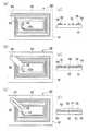
次に、層間絶縁膜を貫通して二層目との導通を図るためのものである層間導通ポスト(導体ポスト)18を形成する。ここでは、上記の1層目配線形成工程と全く同様の工程で層間導通ポストを形成することができる。すなわち、層間導通が必要な場所のみに銀微粒子を含有した導電性インクを吐出し、間に熱風乾燥をはさんで重ねて吐出する。そして合計6回の吐出にて図1(f)に示すように、一層目からの高さが10μmの層間導通ポスト18を形成する。
【0048】
その後、パターン形成された基板10を大気中で摂氏300度にて30分間熱処理して、銀微粒子同士を電気的に接触させる。これにより、1層目の配線パターン17と層間導通ポスト18が一体化した形で形成される。また、この熱処理によって配線パターン17及び層間導通ポスト18全体の膜厚は、図1(g)のように熱処理前の約半分となる。ここで、銀配線パターンの電気伝導度は約2[μΩcm]となる。配線パターン17と基板10との密着力をセロテープ(登録商標)試験による評価を行なうと、剥がれはなく十分な密着力があることがわかる。
【0049】
<層間絶縁膜形成工程>
次に、層間絶縁膜を形成するにあたり、一層目の配線パターン17が形成された基板10に、前処理として波長256nmの紫外線を10[mW/cm2]の強度で5分間照射した。これによって、基板10の表面及び一層目の配線パターン17上が親インク性となる。
【0050】
層間絶縁膜を形成するためのインク21としては、例えば、市販のポリイミドワニス(デュポン社製、製品名「パイルML」)を溶剤(N−メチル−2−ピロリドン)で希釈して、粘度が20[mPa・s]となるように調整して用いた。このインク21を、前述の1層目配線形成工程における導電性パターンの形成で用いた液滴吐出装置と同じ装置にて、層間導電ポスト18の部分を避けるように塗布した。インク滴の量は例えば5ピコリットルとするが、親インク性の基板10表面及び配線パターン17に着弾した後はぬれ広がって、層間導電ポスト部以外の部分はすべてインク21で覆われる。また、インク21の表面は、セルフレベリング効果によって平坦となる。そして、図2(a)で示すように、層間導電ポスト18がインク21の液面から僅かに(0.1μm程度)出る高さまで、液滴吐出装置にて何度かインク21の重ね塗りをする。
【0051】
次いで、この基板10を摂氏400度で30分間熱処理し、溶剤の除去とポリイミドの硬化を行なった。この結果、図2(b)に示すように、ポリイミド22の膜厚は熱処理前のインク21の約半分となる。
そこで、もう一度上記と同様にポリイミド22の上にインク21をパターン塗布し、図2(c)に示すように、層間導電ポスト18がインク21の液面から僅かに出るようにする。そして、上記と同様に摂氏400度で30分間熱処理して硬化させると、図2(d)に示すようにポリイミド22の膜厚は最も薄い部分で例えば合計8μmとなる。
【0052】
この状態では、ポリイミド22の表面には一層目の配線パターンを反映した凹凸が見られる。しかし、もう一度上記と同様のプロセス(ポスト上面が僅かに出るまで高さまで塗布して焼成)を行なえば、さらに平坦に近づく。また、ポリイミド前駆体の塗布を全面に行なわず凹部にのみ塗布して焼成しても同様である。
【0053】
このような工程を何度か繰り返すことにより、ポリイミド22の表面は、その後のプロセスには凹凸がほぼ無視できる程度にまで平坦化することができる。表面の凹凸がそれほど重視されないアプリケーションでは上記ほど平坦化工程を行う必要がない。
なお、以下の実施形態では、説明を簡略化するために図面上ではすべて表面が平坦になったものとして説明している。
以上により、層間導通ポスト18の上面が確実に露出した形で層間絶縁膜(ポリイミド22)を形成することができる。
【0054】
<二層目配線パターン形成工程>
層間絶縁膜(ポリイミド22)の上に、二層目の配線パターン31を形成するには、一層目と全く同様な工程を行う。すなわち、IPA洗浄、紫外線照射洗浄、フッ化アルキルシランによる撥インク化、紫外線照射による接触角の調整、銀微粒子含有インクのパターン吐出、熱風乾燥という各工程を行う。そして、吐出→熱風乾燥→吐出→熱風乾燥という工程を必要な回数だけ繰り返す。
【0055】
さらに多層化する場合には、図3(a)に示すように、1層目と同様にして層間導通ポスト32を形成した後、二層目配線と同時に焼成して導通を図る。その上から1・2層間の層間絶縁膜(ポリイミド22)を形成したときと全く同様に、図3(b)で示すような2、3層間の層間絶縁膜33を形成する。このような工程を必要な回数だけ繰り返すことで、何層でも多層化することができる。図3(c)は三層目まで形成した例である。
【0056】
(第2実施形態)
図4は、本発明の第2実施形態に係る多層配線基板の製造方法を示す工程図である。本実施形態ではコア基板40の両面に多層プリント配線を形成する。
【0057】
第1実施形態と同様にして液滴吐出方式で配線パターンと絶縁膜パターンを積層して形成したのでは、第1実施形態と同様な片面基板しかできない。基板の両面に多層プリント配線を形成するためには、中心となるコア基板40として、通常の両面配線基板を用いて、これを出発点として第1実施形態と同様の工程を両面側に対して行なえばよい。
【0058】
ただし、コア基板40としてはスルーホールがないタイプのものを使うのが好ましく、これは貫通穴を金属ペースト41で充填する方法、片側銅箔基板に銅箔までの非貫通穴をあけて金属ペーストで充填する方法などがある。穴あけは通常のフォトリソグラフィ、またはレーザー照射によって行なう。また、第1実施形態で用いたものと同様の銀微粒子を含有する導電性インクを液滴吐出方式にて貫通穴又は非貫通穴に充填する方法でもよい。
【0059】
このように、コア基板40両面に配線パターンが形成された状態から出発して、層間導通ポスト42を形成する工程、層間絶縁膜43を形成する工程、次の層の配線パターン44を形成する工程、を両面に対して順次繰り返すことにより、コア基板40の両面に多層プリント配線を形成することができる。
【0060】
(第3実施形態)
図5は、本発明の第3実施形態に係る多層配線基板の製造方法を示す工程図である。本実施形態は、チップ・スケール・パッケージ(CSP:Chip Scale Package)手法で再配線を形成するもの、すなわちチップ上にいきなり配線パターンを描画して多層プリント配線を形成するものである。
【0061】
先ず、図5(a)に示すように、アルミパッド51まで形成したICチップ50に、単分子膜を使って撥インク処理をする。この処理は、第1実施形態で行った処理とほとんど同様であり、単分子膜の材料としてデシルトリエトキシシランを用いた以外は第1実施形態の撥インク処理と同じである。
【0062】
次いで、図5(b)に示すように、第1実施形態と同様な工程により、すべてのアルミパッド51の中心に、高さ5μmで直径50μmの層間導電ポスト52を形成する。さらに、第1実施形態と同様な工程により、層間絶縁膜53を層間導電ポスト52の上面と同じ高さまで形成する。これによって、層間導電ポスト52の上面を確実に露出させながら表面が平坦な層間絶縁膜53を形成することができる。
【0063】
その後、上記と同様にして撥インク処理→二層目配線層形成→層間導電ポスト形成→層間絶縁膜形成の工程を行うことで、図5(c)のように、ICチップ50のアルミパッド51から再配線54を形成する。次いで、基板表面に現れている層間導電ポスト52の上に通常のフォトリソグラフィ、又は第1実施形態における配線形成と同様な方法で、パッド55とそのパッド55上に設けられるバンプ56とを形成する。
【0064】
(第4実施形態)
図6は、本発明の第4実施形態に係る多層配線基板の製造方法を示す工程図である。本実施形態は、無線ICカード60におけるアンテナ終端部のコイル形状を上記実施形態の製造方法で形成するものである。なお、図6(a’)、図6(b’)、図6(c’)は、図6(a)、図6(b)、図6(c)における2つのパッド部65間の断面図をそれぞれ示している。
【0065】
この無線ICカード60は、ポリイミドフィルム61に実装されたICチップ63とコイル状のアンテナ62からなる。ICチップ63は、不揮発性メモリ、ロジック回路及び高周波回路などからなり、外部の発信機から出された電波をアンテナ62で捉えて電力供給を受けることにより動作する。また、ICチップ63は、アンテナ62が受信した信号を解析し、その解析結果に対応した必要な所定の信号をアンテナ62から発信させるようになっている。
【0066】
このような無線ICカードを作成するために先ず、第一実施形態の1層目配線形成工程と同様にして、図6(a)に示すように、ポリイミドフィルム61上にコイル状のアンテナ62を形成する。パッド部64やICチップ63を実装する端子部63aもアンテナ62と同時に形成される。アンテナ62を形成した後、、第一実施形態と同様にして、さらにパッド部64の上に層間導通ポスト65を形成する。次いで、第1実施形態と同様にして図6(b)に示すように、層間導通ポスト65の上面が出るようにポリイミドをパターンに塗布して層間絶縁膜66を形成する。
【0067】
層間絶縁膜66を形成した後に、さらに、第1実施形態と同様にして、図6(c)に示すようなパターンに銀微粒子含有の導電性インクを液滴吐出方式で塗布し、その後、焼成してコイル状のアンテナ62の両端を接続する配線67を形成する。最後にICチップ63を異方性導電フィルムを使って図6(C)の位置に実装し、さらに図示しない保護フィルムで全体をラミネートして無線ICカード60となる。
この無線ICカード60は、例えば、5cm離れた外部のリーダー/ライターと通信することができる。
【0068】
なお、パッド部64が数mm角と比較的大きい場合は、層間導通ポスト65を形成しておかなくても、層間の導通に必要な領域を残して層間絶縁膜65を形成することで、多層プリント配線を設けることができる。この場合、層間絶縁層66の端の部分はテーパーを持った形状になるため、その層間絶縁層66の上に断線することなく、液滴吐出方式により配線67を形成することができる。
【0069】
(電子機器)
上記実施形態の多層配線基板の製造方法を用いて製造された基板を備えた電子機器の例について説明する。
図7は、携帯電話の一例を示した斜視図である。図7において、符号1000は携帯電話本体を示し、符号1001は上記実施形態の製造方法で製造された多層配線基板を用いた表示部を示している。
【0070】
図8は、腕時計型電子機器の一例を示した斜視図である。図8において、符号1100は時計本体を示し、符号1101は上記実施形態の製造方法で製造された多層配線基板を用いた表示部を示している。
【0071】
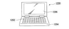
図9は、ワープロ、パソコンなどの携帯型情報処理装置の一例を示した斜視図である。図9において、符号1200は情報処理装置、符号1202はキーボードなどの入力部、符号1204は情報処理装置本体、符号1206は上記実施形態の製造方法で製造された多層配線基板を用いた表示部を示している。
【0072】
図7から図9に示す電子機器は、上記実施形態の製造方法で製造された多層配線基板を備えているので、従来のものよりも簡素な製造工程で精密に製造されるとともに、製造期間を短縮することができる。
【0073】
なお、本発明の技術範囲は上記実施形態に限定されるものではなく、本発明の趣旨を逸脱しない範囲において種々の変更を加えることが可能であり、実施形態で挙げた具体的な材料や層構成及び製造方法などはほんの一例に過ぎず、適宜変更が可能である。
例えば、本発明に係る製造方法は、多層プリント配線の製造に限定されるものではなく、大型ディスプレイ装置などの多層配線に適用することができる。
【0074】
【発明の効果】
以上の説明で明らかなように、本発明によれば、導体ポストの周辺に液滴吐出方式を用いて層間絶縁膜を設けるので、比較的簡素な製造工程で精巧な多層配線を有する電子デバイス、電子機器を得ることが可能となる。
【図面の簡単な説明】
【図1】 本発明の第1実施形態に係る多層配線基板の製造方法を示す工程図である。
【図2】 本発明の第1実施形態に係る多層配線基板の製造方法を示す工程図である。
【図3】 本発明の第1実施形態に係る多層配線基板の製造方法を示す工程図である。
【図4】 本発明の第2実施形態に係る多層配線基板の製造方法を示す工程図である。
【図5】 本発明の第3実施形態に係る多層配線基板の製造方法を示す工程図である。
【図6】 本発明の第4実施形態に係る多層配線基板の製造方法を示す工程図である。
【図7】 本実施形態の電気光学装置を備えた電子機器の一例を示す図である。
【図8】 本実施形態の電気光学装置を備えた電子機器の一例を示す図である。
【図9】 本実施形態の電気光学装置を備えた電子機器の一例を示す図である。
【符号の説明】
10 基板
11 インクジェットヘッド
12,13,15 液滴
14 インク滴
16 パターン
17 配線パターン
18 層間導通ポスト(導体ポスト)
21 インク
22 ポリイミド(層間絶縁膜)
31 配線パターン(二層目)
32 層間導通ポスト
33 層間絶縁膜
40 コア基板
41 金属ペースト
42 層間導通ポスト
43 層間絶縁膜
44 配線パターン
50 ICチップ
51 アルミパッド
52 層間導電ポスト
53 層間絶縁膜
54 再配線
55 パッド
56 バンプ
60 無線ICカード
61 ポリイミドフィルム
62 アンテナ
63 ICチップ
63a ICチップの接続部
64 パッド部
65 層間導通ポスト
66 層間絶縁膜
67 配線[0001]
BACKGROUND OF THE INVENTION
The present invention relates to an electronic device manufacturing method and an electronic device manufacturing method.
[0002]
[Prior art]
Conventionally, as a method of manufacturing a multilayer printed wiring board, there is a method according to the following process. First, each layer is laminated by aligning a single-layer substrate patterned by etching. Next, in order to electrically connect the upper and lower wiring layers, a through hole is formed at a predetermined position of the substrate. Then, the periphery of the through hole is made conductive by plating or the like, or filled with a conductive paste to form a multilayer printed wiring board.
However, this method is difficult to use for high-density mounting because a part mounting pad cannot be formed in the through hole portion, and the diameter of the through hole is usually about 0.3 mm. Met.
[0003]
In recent years, in order to further improve the surface mounting density, a method of establishing an electrical connection between layers by a non-penetrating interlayer connection (interstitial via hole, hereinafter referred to as “IVH”) has been used. By using such a method, the holes formed in the insulating layer are filled with a conductive paste, or the non-through holes provided in the insulating layer using a photosensitive resin are plated with metal. Resin multilayer printed wiring boards that can be used for interlayer connection have been put into practical use.
[0004]
However, each of the above conventional methods employs a technique in which a hole is once formed in the insulating layer, and the inside of the hole is made conductive by plating or a conductive paste, so that the manufacturing process becomes complicated. there were.
[0005]
On the other hand, in Japanese Patent Publication No. 6-57455, a conductor post for interlayer connection is first formed on the lower layer wiring using photolithography instead of making a hole in the insulating layer, and then the conductor post A method is disclosed in which a multilayer wiring is formed by applying a resin around the substrate, forming an insulating film so that the upper surface of the conductor post is exposed by hot pressing, and then forming an upper layer wiring.
Japanese Patent Application Laid-Open No. 9-46045 discloses a method of forming the above-described interlayer connection conductor post by depositing stud bumps, conductive balls, and metal fine particles.
[0006]
[Problems to be solved by the invention]
However, in the method disclosed in the above publication, the lower layer wiring and the interlayer connection conductor post are formed by different methods, which complicates the manufacturing process. In addition, the method disclosed in the above publication has a problem in that it is necessary to completely align the height of the conductor post because the upper surface of the conductor post is exposed by hot pressing after the insulating film is applied over the entire surface. .
[0007]
Japanese Patent Application Laid-Open No. 2000-204479 also discloses a method of selectively forming an insulating film by drawing a solution of an insulator in a desired pattern without making a hole in the insulating layer, and drying by heating. Yes. In the method disclosed in Japanese Patent Laid-Open No. 2000-204479, an activator for electroless plating such as a silane coupling agent is selectively applied to the conductor pattern by a droplet discharge method (inkjet method) or the like. Thereafter, the wiring pattern is selectively formed by performing plating.
Thus, a three-dimensional wiring structure can be formed by applying a pattern so that the insulating layer and the conductor layer are formed in a predetermined order.
[0008]
However, since the conventional technique uses a plating process, it is difficult to form an elaborate pattern having a line / space width of 20 μm / 20 μm, and a waste liquid treatment is required. There was a problem.
[0009]
An object of the present invention is to provide a method for manufacturing an electronic device and a method for manufacturing an electronic apparatus, which can form an elaborate multilayer wiring by a relatively simple manufacturing process.
[0010]
[Means for Solving the Problems]
In order to achieve the above-described object, a method of manufacturing an electronic device according to claim 1 includes a first step of discharging a plurality of conductive inks containing conductive particles from an inkjet head onto a substrate, and the plurality of conductive properties. A second step of drying the ink to form a plurality of ink droplets on the substrate, a third step of disposing the conductive ink from the inkjet head between the plurality of ink droplets, and discharging in the third step A fourth step of drying and drying the conductive ink combined with the ink droplets to form a wiring pattern; a fifth step of discharging the conductive ink from the inkjet head onto the wiring pattern; and discharging in the fifth step A sixth step of drying the conductive ink formed to form a conductor post on the wiring pattern; and A seventh step of discharging onto the conductor post; an eighth step of drying the conductive ink discharged in the seventh step to increase the height of the conductor post; and heating the wiring pattern and the conductor post. A ninth step of integrating, a tenth step of discharging an ink for forming an insulating film from the inkjet head onto the wiring pattern, and a step of drying the ink for forming the insulating film on the wiring pattern. An eleventh step of forming an insulating film and projecting at least a part of the conductor post from the insulating film; forming a second-layer wiring pattern on the insulating film; and the wiring pattern and the second-layer wiring pattern And the twelfth step for connecting the conductor post and the second-layer wiring pattern.
The electronic device manufacturing method according to claim 2 includes the step of irradiating the substrate with ultraviolet rays before the first step in the electronic device manufacturing method according to claim 1. To do.
The electronic device manufacturing method according to claim 3 is the electronic device manufacturing method according to claim 1 or 2, wherein the wiring pattern and the conductor post have conductivity before the ninth step. It is characterized by not.
The electronic device manufacturing method according to claim 4 is the electronic device manufacturing method according to any one of claims 1 to 3, wherein the wiring pattern and the conductor post are electrically conductive after the ninth step. The wiring pattern and the conductor post are electrically connected.
An electronic device manufacturing method according to claim 5 is the electronic device manufacturing method according to any one of claims 1 to 4, wherein the conductive particles are silver fine particles.
An electronic device manufacturing method according to claim 6 is the electronic device manufacturing method according to any one of claims 1 to 5, wherein the second step includes a heating step, and the plurality of conductive inks are heated. The temperature to perform is lower than the temperature which heats the said wiring pattern and the said conductor post in the said 9th process.
[0011]
According to such a method, since the photolithography, etching and drilling steps are not required in forming the interlayer insulating film, the manufacturing process of the multilayer wiring board can be simplified, and the manufacturing apparatus can be reduced in size. , Shortening the manufacturing period and reducing the manufacturing cost.
Further, according to such a method, a mask is not necessary for forming an interlayer insulating film, and therefore, for example, an interlayer insulating film can be formed directly from CAD data, and a period from design to completion can be increased. It is shortened and it becomes possible to easily cope with design changes. Further, according to such a method, since the interlayer insulating film is provided by the droplet discharge method, the interlayer insulating film can be formed in a state where the upper surface of the conductor post is reliably exposed.
Further, according to such a method, due to the self-leveling effect, even if there are some steps in the lower layer wiring, a flat surface in which the upper surface of the conductor post and the upper surface of the interlayer insulating film formed on the lower layer wiring are aligned. Thus, a multilayer wiring board having a good structure can be formed.
Further, according to such a method, a mask is not necessary for forming the conductor post, and therefore, for example, the conductor post can be formed directly from CAD data, and the period from design to completion is shortened. It becomes possible to easily cope with design changes.
Also, according to such a method, photolithography, etching and drilling steps are not required in forming the wiring, so that the manufacturing process of the multilayer wiring board can be simplified, and the manufacturing apparatus can be reduced in size. , Shortening the manufacturing period and reducing the manufacturing cost.
In addition, according to such a method, a mask is not necessary for forming the wiring. For example, it is possible to form a conductor post directly from CAD data, and a period from design to completion is shortened. It becomes possible to easily cope with design changes.
In addition, according to such a method, since the photolithography, etching and drilling steps are not required for all the steps of the multilayer wiring board, the manufacturing process of the multilayer wiring board can be greatly simplified. The manufacturing apparatus can be downsized, the manufacturing period can be shortened, and the manufacturing cost can be reduced.
In addition, according to such a method, a mask is not necessary for all the steps of the multilayer wiring board. For example, the multilayer wiring board can be formed directly from CAD data, and the period from design to completion is further increased. It is shortened and it becomes possible to easily cope with design changes.
In addition, according to such a method, the droplet discharge device has a plurality of discharge heads, or a plurality of liquid (ink) nozzles in one head as in a color inkjet printer for normal image printing. If the head is structured so as to be supplied separately to the group, the interlayer insulating film, wiring layer and conductor post can be formed with a single droplet discharge device by simply replacing the electronic file (bitmap) for controlling the coating pattern. Therefore, the manufacturing period can be further shortened and the manufacturing cost can be reduced, and the design change can be easily handled.
In addition, according to such a method, the thickness of the conductive film forming the wiring or the conductor post is gradually increased by alternately repeating the discharge of the conductive ink onto the substrate and the drying, thereby obtaining a desired thickness and Can be height.
Further, according to such a method, after the conductive ink (solvent) containing metal fine particles is dried, the coating film has liquid repellency with respect to the conductive ink containing the same metal fine particles. Even if the conductive ink is applied over the coating film, there is an effect that only the film thickness in the height direction can be obtained without spreading. Therefore, by utilizing this effect, the conductor post can be formed only in a necessary portion.
Further, according to such a method, the width of the wiring can be narrowed, and a more precise wiring structure can be formed.
Moreover, according to such a method, it becomes easy to form wiring and a conductor post in a predetermined position.
Moreover, according to such a method, electrical conductivity can be expressed in the conductive ink discharged onto the substrate. That is, since the electrical conductivity is not exhibited only by drying the conductive ink, the electrical conductivity is exhibited by firing.
In addition, according to such a method, for example, a polyimide precursor is diluted with a solvent to a viscosity that enables droplet ejection, and after droplet ejection, firing is performed at 300 degrees Celsius, thereby providing interlayer insulation. A film can be formed.
Also, according to such a method, it is possible to form a multilayer wiring board having a good structure in which the height (film thickness) of the interlayer insulating film and the height (film thickness) of the conductor posts are substantially the same.
In addition, according to such a method, when a self-leveling effect can be expected when applying a pattern by the droplet discharge method, the negative pattern of the bitmap used to form the conductor post is used as it is (conductor). Application can be made to form an interlayer insulating film (apart from the post portion). On the other hand, when the self-leveling effect cannot be expected so much, after applying for forming the interlayer insulating film until the same height as the lower layer wiring is avoided, avoid the portion of the conductor post so as to avoid the lower layer wiring once. The same application is performed as described above. Finally, baking is performed to complete an interlayer insulating film made of polyimide or the like.
Moreover, according to such a method, a multilayer wiring board can be manufactured with a simple manufacturing process. That is, for example, after the upper surface of the conductor post is exposed and the other portions are covered with an interlayer insulating film having the same height as the upper surface of the conductor post, the substrate is again subjected to water repellency treatment and a droplet discharge method. In principle, a multilayer wiring having no limit on the number of layers can be formed by repeating a predetermined number of times of wiring formation and conductive post formation, firing, interlayer insulation film formation, firing, and the like.
Further, according to such a method, a multilayer wiring can be formed on a IC (integrated circuit) chip suddenly by droplet discharge.
In addition, according to such a method, a multilayer wiring using the method for manufacturing a multilayer wiring board of the present invention is applied to a substrate formed halfway by a manufacturing method different from the method for manufacturing a multilayer wiring board of the present invention. Can be formed. This method is suitable for dealing with double-sided mounting, for example. For example, after forming a pattern on the innermost substrate, or by opening a through hole in front of it and filling it with a metal paste or the like, and then using the manufacturing method of the present invention from the step of standing a conductor post, A multilayer wiring board mounted on both sides can be formed using only the droplet discharge method.
[0034]
An electronic device manufacturing method according to a seventh aspect includes the electronic device manufacturing method according to any one of the first to sixth aspects.
According to the present invention, it is possible to reduce the manufacturing cost and reduce the size while shortening the manufacturing time of the electronic device.
[0036]
DETAILED DESCRIPTION OF THE INVENTION
Hereinafter, the manufacturing method of the multilayer wiring board concerning the present invention is explained based on a drawing.
(First embodiment)
1 to 3 are process diagrams showing a method of manufacturing a multilayer wiring board according to the first embodiment of the present invention. FIG. 1 shows the process from the ink repellent treatment process to the interlayer post formation. FIG. 2 shows an interlayer insulating film forming step. FIG. 3 shows steps after the formation of the second-layer wiring pattern. In this embodiment, a multilayer printed wiring is formed on one side of the
[0037]
<Conductive ink>
First, a conductive ink that is a liquid discharged from a droplet discharge device and is used when forming a multilayer printed wiring will be described. In this embodiment, a gold fine particle dispersion (trade name “Perfect Gold” manufactured by Vacuum Metallurgical Co., Ltd.) in which gold fine particles having a diameter of about 10 nm are dispersed in toluene is diluted with toluene, and the viscosity is 3 [mPa · s]. The liquid is used as a conductive ink.
[0038]
<Ink repellent treatment process>
Next, an ink repellent process (water repellent process) performed on the surface of the substrate will be described. By performing this ink repellent treatment, the position of the conductive ink or the like discharged on the substrate can be controlled with higher accuracy. First, the
[0039]
The contact angle between the substrate surface after the ink repellent treatment and the conductive ink is too large to form a multilayer printed wiring by the droplet discharge method. Therefore, the
A receiving layer may be formed instead of the ink repellent treatment.
[0040]
<First-layer wiring formation process>
The conductive ink is discharged onto the
[0041]
Here, as the
[0042]
As a wiring pattern drawn on the
[0043]
Under the above conditions, one
[0044]
Even after this process, the ink repellency of the
[0045]
Thereafter, as shown in FIG. 1C, the
In this discharge, since the liquid repellency on the
[0046]
Thereafter, the
Furthermore, in order to increase the film thickness and to prevent the dot shape from remaining in the wiring pattern, the discharge and hot air drying processes aiming at the middle of the dots are performed in the same manner as described above. The
[0047]
<Interlayer conduction post formation process>
Next, an interlayer conduction post (conductor post) 18 is formed to penetrate the interlayer insulating film and to establish conduction with the second layer. Here, the interlayer conductive post can be formed in the same process as the first layer wiring forming process. That is, a conductive ink containing silver fine particles is discharged only in a place where interlayer conduction is necessary, and is discharged while being overlapped with hot air drying. Then, as shown in FIG. 1F, the interlayer
[0048]
Thereafter, the patterned
[0049]
<Interlayer insulating film formation process>
Next, when forming the interlayer insulating film, the
[0050]
As the
[0051]
Next, the
Therefore, once again, the
[0052]
In this state, the surface of the
[0053]
By repeating such a process several times, the surface of the
In the following embodiments, in order to simplify the description, it is assumed that the surface is all flat on the drawings.
As described above, the interlayer insulating film (polyimide 22) can be formed in such a manner that the upper surface of the interlayer
[0054]
<Second-layer wiring pattern formation process>
In order to form the
[0055]
In the case of further multilayering, as shown in FIG. 3A, the interlayer
[0056]
(Second Embodiment)
FIG. 4 is a process diagram showing a method for manufacturing a multilayer wiring board according to the second embodiment of the present invention. In the present embodiment, multilayer printed wiring is formed on both surfaces of the
[0057]
If the wiring pattern and the insulating film pattern are stacked by the droplet discharge method in the same manner as in the first embodiment, only a single-sided substrate similar to that in the first embodiment can be formed. In order to form a multilayer printed wiring on both sides of the substrate, a normal double-sided wiring substrate is used as the
[0058]
However, it is preferable to use a
[0059]
Thus, starting from the state where the wiring patterns are formed on both surfaces of the
[0060]
(Third embodiment)
FIG. 5 is a process diagram showing a method for manufacturing a multilayer wiring board according to a third embodiment of the present invention. In the present embodiment, rewiring is formed by a chip scale package (CSP) method, that is, a multilayer printed wiring is formed by drawing a wiring pattern on the chip suddenly.
[0061]
First, as shown in FIG. 5A, the
[0062]
Next, as shown in FIG. 5B, an interlayer
[0063]
After that, by performing the steps of ink repellent treatment → second-layer wiring layer formation → interlayer conductive post formation → interlayer insulating film formation in the same manner as described above, the
[0064]
(Fourth embodiment)
FIG. 6 is a process diagram showing a method for manufacturing a multilayer wiring board according to a fourth embodiment of the present invention. In the present embodiment, the coil shape of the antenna terminal portion in the
[0065]
The
[0066]
In order to create such a wireless IC card, first, as shown in FIG. 6A, a
[0067]
After forming the
The
[0068]
When the
[0069]
(Electronics)
An example of an electronic device provided with a substrate manufactured using the method for manufacturing a multilayer wiring board according to the embodiment will be described.
FIG. 7 is a perspective view showing an example of a mobile phone. In FIG. 7,
[0070]
FIG. 8 is a perspective view showing an example of a wristwatch type electronic apparatus. In FIG. 8,
[0071]
FIG. 9 is a perspective view showing an example of a portable information processing apparatus such as a word processor or a personal computer. In FIG. 9,
[0072]
Since the electronic device shown in FIGS. 7 to 9 includes the multilayer wiring board manufactured by the manufacturing method of the above-described embodiment, the electronic device is precisely manufactured by a simpler manufacturing process than the conventional one, and the manufacturing period is increased. It can be shortened.
[0073]
The technical scope of the present invention is not limited to the above-described embodiment, and various modifications can be made without departing from the spirit of the present invention, and the specific materials and layers mentioned in the embodiment can be added. The configuration and the manufacturing method are merely examples, and can be changed as appropriate.
For example, the manufacturing method according to the present invention is not limited to the manufacture of multilayer printed wiring, but can be applied to multilayer wiring such as large display devices.
[0074]
【The invention's effect】
As is apparent from the above description, according to the present invention, since the interlayer insulating film is provided around the conductor post using a droplet discharge method, an electronic device having a sophisticated multilayer wiring in a relatively simple manufacturing process, An electronic device can be obtained.
[Brief description of the drawings]
FIG. 1 is a process diagram showing a method for manufacturing a multilayer wiring board according to a first embodiment of the present invention.
FIG. 2 is a process diagram showing a method for manufacturing a multilayer wiring board according to the first embodiment of the present invention.
FIG. 3 is a process chart showing the method for manufacturing a multilayer wiring board according to the first embodiment of the present invention.
FIG. 4 is a process diagram showing a method for manufacturing a multilayer wiring board according to a second embodiment of the present invention.
FIG. 5 is a process diagram showing a method for manufacturing a multilayer wiring board according to a third embodiment of the present invention.
FIG. 6 is a process diagram showing a method for manufacturing a multilayer wiring board according to a fourth embodiment of the present invention.
FIG. 7 is a diagram illustrating an example of an electronic apparatus including the electro-optical device according to the embodiment.
FIG. 8 is a diagram illustrating an example of an electronic apparatus including the electro-optical device according to the embodiment.
FIG. 9 is a diagram illustrating an example of an electronic apparatus including the electro-optical device according to the embodiment.
[Explanation of symbols]
10
21
31 Wiring pattern (second layer)
32 Interlayer
Claims (7)
Translated fromJapanese前記複数の導電性インクを乾燥させ前記基板上に複数のインク滴を形成する第二工程と、
前記導電性インクをインクジェットヘッドから前記複数のインク滴同士の間に配置する第三工程と、
前記第三工程において吐出した導電性インクを乾燥させ前記インク滴と結合させて配線パターンを形成する第四工程と、
前記導電性インクをインクジェットヘッドから前記配線パターン上に吐出する第五工程と、
前記第五工程において吐出した導電性インクを乾燥させて前記配線パターン上に導体ポストを形成する第六工程と、
前記導電性インクをインクジェットヘッドから前記導体ポスト上に吐出する第七工程と、
前記第七工程において吐出した導電性インクを乾燥させ前記導体ポストの高さを増加させる第八工程と、
前記配線パターンと前記導体ポストとを加熱して一体化させる第九工程と、
絶縁膜を形成するためのインクをインクジェットヘッドから前記配線パターン上に吐出する第十工程と、
前記絶縁膜を形成するためのインクを乾燥させ前記配線パターン上に前記絶縁膜を形成し、前記導体ポストの少なくとも一部を前記絶縁膜から突出させる第十一工程と、
前記絶縁膜上に二層目配線パターンを形成し、前記配線パターンと前記二層目配線パターンとを前記絶縁膜により絶縁し、前記導体ポストと前記二層目配線パターンとを接続する第十二工程と、
を含むことを特徴とする電子デバイスの製造方法。A first step of discharging a plurality of conductive inks containing conductive particles from an inkjet head onto a substrate;
A second step of drying the plurality of conductive inks to form a plurality of ink droplets on the substrate;
A third step of disposing the conductive ink between the plurality of ink droplets from an inkjet head;
A fourth step of drying the conductive ink discharged in the third step and combining it with the ink droplets to form a wiring pattern;
A fifth step of discharging the conductive ink from the inkjet head onto the wiring pattern;
A sixth step of drying the conductive ink discharged in the fifth step to form a conductor post on the wiring pattern;
A seventh step of discharging the conductive ink from the inkjet head onto the conductor post;
An eighth step of drying the conductive ink discharged in the seventh step and increasing the height of the conductor post;
A ninth step of heating and integrating the wiring pattern and the conductor post;
A tenth step of discharging ink for forming an insulating film from the inkjet head onto the wiring pattern;
An eleventh step of drying the ink for forming the insulating film, forming the insulating film on the wiring pattern, and projecting at least a part of the conductor post from the insulating film;
A twelfth wiring pattern is formed on the insulating film, the wiring pattern and the second wiring pattern are insulated by the insulating film, and the conductor post and the second wiring pattern are connected. Process,
The manufacturing method of the electronic device characterized by the above-mentioned.
前記第一工程の前に、前記基板上に紫外線を照射する工程を含むことを特徴とする電子デバイスの製造方法。In the manufacturing method of the electronic device of Claim 1,
A method of manufacturing an electronic device, comprising a step of irradiating the substrate with ultraviolet rays before the first step.
前記第九工程の前に、前記配線パターンと前記導体ポストとが導電性を有さないことを特徴とする電子デバイスの製造方法。In the manufacturing method of the electronic device of Claim 1 or 2,
Prior to the ninth step, the wiring pattern and the conductor post do not have electrical conductivity.
前記第九工程の後に、前記配線パターンと前記導体ポストとが導電性を有し、前記配線パターンと前記導体ポストとが電気的に接続することを特徴とする電子デバイスの製造方法。In the manufacturing method of the electronic device in any one of Claim 1 thru | or 3,
After the ninth step, the wiring pattern and the conductor post have conductivity, and the wiring pattern and the conductor post are electrically connected to each other.
前記導電性粒子が銀微粒子であることを特徴とする電子デバイスの製造方法。In the manufacturing method of the electronic device in any one of Claims 1 thru | or 4,
The method for producing an electronic device, wherein the conductive particles are silver fine particles.
前記第二工程が加熱工程を含み、前記複数の導電性インクを加熱する温度が前記第九工程において前記配線パターンと前記導体ポストとを加熱する温度より低いことを特徴とする電子デバイスの製造方法。In the manufacturing method of the electronic device in any one of Claim 1 thru | or 5,
The method of manufacturing an electronic device, wherein the second step includes a heating step, and a temperature for heating the plurality of conductive inks is lower than a temperature for heating the wiring pattern and the conductor post in the ninth step. .
Priority Applications (4)
| Application Number | Priority Date | Filing Date | Title |
|---|---|---|---|
| JP2002113621AJP3925283B2 (en) | 2002-04-16 | 2002-04-16 | Method for manufacturing electronic device, method for manufacturing electronic device |
| EP03252346AEP1355522A3 (en) | 2002-04-16 | 2003-04-14 | Multilayered wiring board, method of producing multilayered wiring board, electronic device and electronic apparatus |
| CNB031104312ACN1284431C (en) | 2002-04-16 | 2003-04-15 | Multilayer wiring substrate, method for mfg. same, electronic device and electronic machine |
| US10/417,398US7285305B2 (en) | 2002-04-16 | 2003-04-16 | Multilayered wiring board, method of producing multilayered wiring board, electronic device and electronic apparatus |
Applications Claiming Priority (1)
| Application Number | Priority Date | Filing Date | Title |
|---|---|---|---|
| JP2002113621AJP3925283B2 (en) | 2002-04-16 | 2002-04-16 | Method for manufacturing electronic device, method for manufacturing electronic device |
Related Child Applications (2)
| Application Number | Title | Priority Date | Filing Date |
|---|---|---|---|
| JP2006074159ADivisionJP2006179953A (en) | 2006-03-17 | 2006-03-17 | Multilayer wiring board, electronic device and electronic equipment |
| JP2007000466ADivisionJP2007116193A (en) | 2007-01-05 | 2007-01-05 | Multilayer wiring board manufacturing method, electronic device, electronic equipment |
Publications (2)
| Publication Number | Publication Date |
|---|---|
| JP2003309369A JP2003309369A (en) | 2003-10-31 |
| JP3925283B2true JP3925283B2 (en) | 2007-06-06 |
Family
ID=28672616
Family Applications (1)
| Application Number | Title | Priority Date | Filing Date |
|---|---|---|---|
| JP2002113621AExpired - Fee RelatedJP3925283B2 (en) | 2002-04-16 | 2002-04-16 | Method for manufacturing electronic device, method for manufacturing electronic device |
Country Status (4)
| Country | Link |
|---|---|
| US (1) | US7285305B2 (en) |
| EP (1) | EP1355522A3 (en) |
| JP (1) | JP3925283B2 (en) |
| CN (1) | CN1284431C (en) |
Families Citing this family (60)
| Publication number | Priority date | Publication date | Assignee | Title |
|---|---|---|---|---|
| DE10256662A1 (en) | 2002-12-04 | 2004-06-17 | Robert Bosch Gmbh | Fuel injector |
| KR100484168B1 (en)* | 2002-10-11 | 2005-04-19 | 삼성전자주식회사 | Ink jet printhead and manufacturing method thereof |
| JP2004337701A (en)* | 2003-05-14 | 2004-12-02 | Seiko Epson Corp | Droplet discharging method and droplet discharging device |
| WO2005048354A1 (en) | 2003-11-14 | 2005-05-26 | Semiconductor Energy Laboratory Co., Ltd. | Semiconductor element, method for manufacturing the same, liquid crystal display device, and method for manufacturing the same |
| WO2005048223A1 (en) | 2003-11-14 | 2005-05-26 | Semiconductor Energy Laboratory Co., Ltd. | Light-emitting device and method for manufacturing the same |
| US20070123027A1 (en)* | 2003-12-22 | 2007-05-31 | Michinori Shinkai | Wiring forming method, wiring forming apparatus, and wiring board |
| JP4281584B2 (en) | 2004-03-04 | 2009-06-17 | セイコーエプソン株式会社 | Manufacturing method of semiconductor device |
| JP2005268543A (en)* | 2004-03-18 | 2005-09-29 | Hitachi Chem Co Ltd | Insulating layer and material for forming the same |
| JP4193758B2 (en)* | 2004-06-18 | 2008-12-10 | セイコーエプソン株式会社 | Layer forming device |
| US20060033793A1 (en)* | 2004-08-10 | 2006-02-16 | Webster Grant A | Coupling agent patterning |
| JP4683180B2 (en)* | 2004-08-19 | 2011-05-11 | セイコーエプソン株式会社 | Wiring board manufacturing method and multilayer wiring board manufacturing method |
| JP4506809B2 (en)* | 2004-08-20 | 2010-07-21 | セイコーエプソン株式会社 | MULTILAYER STRUCTURE FORMING METHOD, WIRING BOARD AND ELECTRONIC DEVICE MANUFACTURING METHOD |
| JP4052295B2 (en)* | 2004-08-25 | 2008-02-27 | セイコーエプソン株式会社 | MULTILAYER WIRING BOARD MANUFACTURING METHOD, ELECTRONIC DEVICE, AND ELECTRONIC DEVICE |
| JP4100385B2 (en) | 2004-09-22 | 2008-06-11 | セイコーエプソン株式会社 | Multilayer structure forming method, wiring board manufacturing method, and electronic device manufacturing method |
| JP3928638B2 (en) | 2004-09-28 | 2007-06-13 | セイコーエプソン株式会社 | Wiring board manufacturing method and electronic device |
| JP2006100401A (en) | 2004-09-28 | 2006-04-13 | Seiko Epson Corp | Wiring pattern forming method, wiring pattern, electronic device |
| CN100415518C (en)* | 2004-09-28 | 2008-09-03 | 精工爱普生株式会社 | Forming method of wiring pattern |
| JP4506384B2 (en)* | 2004-09-28 | 2010-07-21 | セイコーエプソン株式会社 | PATTERN FORMING METHOD, WIRING BOARD MANUFACTURING METHOD, AND ELECTRONIC DEVICE |
| JP2006156943A (en) | 2004-09-28 | 2006-06-15 | Seiko Epson Corp | Wiring pattern forming method, wiring pattern, and electronic device |
| JP4297106B2 (en)* | 2005-02-23 | 2009-07-15 | セイコーエプソン株式会社 | Film pattern forming method, device manufacturing method, electro-optical device, and electronic apparatus |
| US7765686B2 (en) | 2005-03-14 | 2010-08-03 | Ricoh Company, Ltd. | Multilayer wiring structure and method of manufacturing the same |
| JP4293181B2 (en)* | 2005-03-18 | 2009-07-08 | セイコーエプソン株式会社 | Metal particle dispersion, method for producing metal particle dispersion, method for producing conductive film-formed substrate, electronic device and electronic apparatus |
| JP2006332094A (en) | 2005-05-23 | 2006-12-07 | Seiko Epson Corp | Method for manufacturing electronic substrate, method for manufacturing semiconductor device, and method for manufacturing electronic device |
| US8147903B2 (en) | 2005-06-22 | 2012-04-03 | Canon Kabushiki Kaisha | Circuit pattern forming method, circuit pattern forming device and printed circuit board |
| US7829135B2 (en)* | 2005-06-22 | 2010-11-09 | Canon Kabushiki Kaisha | Method and apparatus for forming multi-layered circuit pattern |
| JP4379386B2 (en)* | 2005-06-23 | 2009-12-09 | セイコーエプソン株式会社 | Multilayer structure forming method |
| JP4742715B2 (en)* | 2005-07-19 | 2011-08-10 | セイコーエプソン株式会社 | Wiring pattern forming method and wiring board manufacturing method |
| JP2007088004A (en)* | 2005-09-20 | 2007-04-05 | Seiko Epson Corp | Multilayer circuit board manufacturing method, multilayer circuit board, electro-optical device, and electronic apparatus |
| JP5021216B2 (en)* | 2006-02-22 | 2012-09-05 | イビデン株式会社 | Printed wiring board and manufacturing method thereof |
| US20070248798A1 (en)* | 2006-04-19 | 2007-10-25 | Canon Kabushiki Kaisha | Circuit board manufacturing process, circuit board manufactured by the process, and circuit board manufacturing apparatus |
| US20070281091A1 (en)* | 2006-05-31 | 2007-12-06 | Cabot Corporation | Polyimide insulative layers in multi-layered printed electronic features |
| JP2008066576A (en)* | 2006-09-08 | 2008-03-21 | Seiko Epson Corp | Method of manufacturing circuit board |
| US20080119011A1 (en)* | 2006-11-20 | 2008-05-22 | Industrial Technology Research Institute | Method of film coating and device manufactured thereby |
| US20100065318A1 (en)* | 2006-11-28 | 2010-03-18 | Kyocera Corporation | Circuit board and semiconductor element mounted structure using the same |
| KR100871034B1 (en)* | 2007-06-12 | 2008-11-27 | 삼성전기주식회사 | Paste bump formation method of printed circuit board |
| TWI360205B (en) | 2007-06-20 | 2012-03-11 | Princo Corp | Multi-layer substrate and manufacture method there |
| JP2010532923A (en)* | 2007-07-12 | 2010-10-14 | 巨擘科技股▲ふん▼有限公司 | Multilayer substrate and manufacturing method thereof |
| KR101044103B1 (en)* | 2008-04-03 | 2011-06-28 | 삼성전기주식회사 | Multilayer printed circuit board and its manufacturing method |
| KR100969437B1 (en)* | 2008-06-13 | 2010-07-14 | 삼성전기주식회사 | Printed circuit board and manufacturing method thereof |
| GB2462290B (en)* | 2008-07-31 | 2011-02-23 | Novalia Ltd | Printed article |
| JP2010087208A (en)* | 2008-09-30 | 2010-04-15 | Fujifilm Corp | Method for forming three-dimensional structure, method for manufacturing semiconductor device, and semiconductor device |
| JP2011134879A (en)* | 2009-12-24 | 2011-07-07 | Seiko Epson Corp | Method for producing build-up substrate |
| US8476538B2 (en)* | 2010-03-08 | 2013-07-02 | Formfactor, Inc. | Wiring substrate with customization layers |
| KR20110113980A (en)* | 2010-04-12 | 2011-10-19 | 삼성전자주식회사 | Multilayer printed circuit board including film and manufacturing method thereof |
| JP5541017B2 (en)* | 2010-09-08 | 2014-07-09 | 日立化成株式会社 | Insulating layer forming material and insulating layer |
| US8617926B2 (en)* | 2010-09-09 | 2013-12-31 | Advanced Micro Devices, Inc. | Semiconductor chip device with polymeric filler trench |
| JP5849489B2 (en)* | 2011-07-21 | 2016-01-27 | セイコーエプソン株式会社 | Electro-optical device, projection display device, electronic apparatus, and method of manufacturing electro-optical device |
| JP5670372B2 (en)* | 2012-03-29 | 2015-02-18 | 富士フイルム株式会社 | Liquid ejection apparatus and control method thereof |
| FR3000598B1 (en)* | 2012-12-27 | 2016-05-06 | Commissariat Energie Atomique | IMPROVED METHOD FOR PRODUCING A CONTACT RESUME STRUCTURE |
| WO2014194049A1 (en)* | 2013-05-31 | 2014-12-04 | The Regents Of The University Of California | Through silicon vias and thermocompression bonding using inkjet-printed nanoparticles |
| JP6370077B2 (en)* | 2014-03-25 | 2018-08-08 | 株式会社Fuji | Electronic device manufacturing method and manufacturing apparatus |
| US9357640B2 (en) | 2014-09-22 | 2016-05-31 | Oce'-Technologies B.V. | Method of manufacturing a multi-layer printed circuit board |
| EP3318113A1 (en)* | 2015-06-30 | 2018-05-09 | 3M Innovative Properties Company | Electronic devices comprising a via and methods of forming such electronic devices |
| WO2017047323A1 (en)* | 2015-09-18 | 2017-03-23 | コニカミノルタ株式会社 | Wiring laminated structural body forming method |
| US10257930B2 (en)* | 2016-06-22 | 2019-04-09 | R&D Circuits, Inc. | Trace anywhere interconnect |
| CN109428007B (en)* | 2017-08-29 | 2020-06-26 | 京东方科技集团股份有限公司 | Preparation method of display substrate, display substrate and display device |
| JP7142781B2 (en)* | 2019-06-18 | 2022-09-27 | 株式会社Fuji | Wiring board manufacturing method and wiring board manufacturing apparatus |
| US12048102B2 (en)* | 2019-07-30 | 2024-07-23 | Fuji Corporation | Electronic circuit production method using 3D layer shaping |
| EP4209280A4 (en) | 2020-09-03 | 2024-02-28 | Konica Minolta, Inc. | METHOD FOR PATTERN FORMATION |
| FR3147480A1 (en)* | 2023-04-03 | 2024-10-04 | Ico Novation | Process for manufacturing a printed circuit board |
Family Cites Families (26)
| Publication number | Priority date | Publication date | Assignee | Title |
|---|---|---|---|---|
| US4668533A (en)* | 1985-05-10 | 1987-05-26 | E. I. Du Pont De Nemours And Company | Ink jet printing of printed circuit boards |
| EP0247575B1 (en)* | 1986-05-30 | 1993-07-21 | Furukawa Denki Kogyo Kabushiki Kaisha | Multilayer printed wiring board and method for producing the same |
| JPH0797602B2 (en)* | 1988-05-06 | 1995-10-18 | 日本電気株式会社 | Semiconductor integrated circuit device |
| FR2650472A1 (en)* | 1989-07-27 | 1991-02-01 | Bull Sa | METHOD FOR DEPOSITING AN INSULATING LAYER ON A CONDUCTIVE LAYER OF THE MULTI-LAYER NETWORK OF A HIGH DENSITY INTEGRATED CIRCUIT CONNECTION CARD, AND RESULTING CARD |
| US5948533A (en)* | 1990-02-09 | 1999-09-07 | Ormet Corporation | Vertically interconnected electronic assemblies and compositions useful therefor |
| JPH0710030B2 (en)* | 1990-05-18 | 1995-02-01 | インターナシヨナル・ビジネス・マシーンズ・コーポレーシヨン | Method for manufacturing multilayer wiring board |
| US6175422B1 (en) | 1991-01-31 | 2001-01-16 | Texas Instruments Incorporated | Method and apparatus for the computer-controlled manufacture of three-dimensional objects from computer data |
| US5594652A (en)* | 1991-01-31 | 1997-01-14 | Texas Instruments Incorporated | Method and apparatus for the computer-controlled manufacture of three-dimensional objects from computer data |
| JPH07231154A (en) | 1994-02-21 | 1995-08-29 | Matsushita Electric Works Ltd | Method of forming three-dimensional circuit |
| KR100280298B1 (en)* | 1995-11-17 | 2001-02-01 | 니시무로 타이죠 | Multi-layered wiring board, prefabricated material of multi-layered wiring board, manufacturing method of multilayered wiring board, method of forming electronic component, electronic component package and conductive filler |
| US5650199A (en)* | 1995-11-22 | 1997-07-22 | Aem, Inc. | Method of making a multilayer electronic component with inter-layer conductor connection utilizing a conductive via forming ink |
| JPH10326559A (en)* | 1997-03-21 | 1998-12-08 | Canon Inc | Printed circuit board, electron-emitting device, electron source, and method of manufacturing image forming apparatus |
| JPH1154928A (en) | 1997-06-03 | 1999-02-26 | Ngk Spark Plug Co Ltd | Wiring board and its manufacture |
| ATE434259T1 (en)* | 1997-10-14 | 2009-07-15 | Patterning Technologies Ltd | METHOD OF MAKING AN ELECTRICAL CAPACITOR |
| JPH11163499A (en) | 1997-11-28 | 1999-06-18 | Nitto Boseki Co Ltd | Manufacturing method of printed wiring board and printed wiring board by this manufacturing method |
| US6487774B1 (en)* | 1998-01-22 | 2002-12-03 | Matsushita Electric Industrial Co., Ltd. | Method of forming an electronic component using ink |
| US6261941B1 (en)* | 1998-02-12 | 2001-07-17 | Georgia Tech Research Corp. | Method for manufacturing a multilayer wiring substrate |
| JP4741045B2 (en) | 1998-03-25 | 2011-08-03 | セイコーエプソン株式会社 | Electric circuit, manufacturing method thereof and electric circuit manufacturing apparatus |
| JPH11274681A (en) | 1998-03-25 | 1999-10-08 | Seiko Epson Corp | Electronic device and manufacturing method thereof |
| JP2000294930A (en) | 1999-04-06 | 2000-10-20 | Mitsubishi Electric Corp | Method of manufacturing multilayer printed board and semiconductor device using this multilayer printed board |
| JP2001267725A (en) | 2000-03-16 | 2001-09-28 | Matsushita Electric Ind Co Ltd | Method of manufacturing ceramic thick film printed circuit board |
| JP2001267308A (en) | 2000-03-22 | 2001-09-28 | Seiko Epson Corp | Protective film forming apparatus and semiconductor manufacturing apparatus using the same |
| TW515064B (en) | 2000-03-23 | 2002-12-21 | Seiko Epson Corp | Semiconductor device and its manufacturing method, circuit board and electronic machine |
| US7442408B2 (en)* | 2002-03-26 | 2008-10-28 | Hewlett-Packard Development Company, L.P. | Methods for ink-jet printing circuitry |
| JP3801158B2 (en)* | 2002-11-19 | 2006-07-26 | セイコーエプソン株式会社 | MULTILAYER WIRING BOARD MANUFACTURING METHOD, MULTILAYER WIRING BOARD, ELECTRONIC DEVICE, AND ELECTRONIC DEVICE |
| US7202155B2 (en)* | 2003-08-15 | 2007-04-10 | Semiconductor Energy Laboratory Co., Ltd. | Method for manufacturing wiring and method for manufacturing semiconductor device |
- 2002
- 2002-04-16JPJP2002113621Apatent/JP3925283B2/ennot_activeExpired - Fee Related
- 2003
- 2003-04-14EPEP03252346Apatent/EP1355522A3/ennot_activeWithdrawn
- 2003-04-15CNCNB031104312Apatent/CN1284431C/ennot_activeExpired - Fee Related
- 2003-04-16USUS10/417,398patent/US7285305B2/ennot_activeExpired - Fee Related
Also Published As
| Publication number | Publication date |
|---|---|
| CN1452451A (en) | 2003-10-29 |
| EP1355522A3 (en) | 2004-11-10 |
| CN1284431C (en) | 2006-11-08 |
| US20040000429A1 (en) | 2004-01-01 |
| JP2003309369A (en) | 2003-10-31 |
| US7285305B2 (en) | 2007-10-23 |
| EP1355522A2 (en) | 2003-10-22 |
Similar Documents
| Publication | Publication Date | Title |
|---|---|---|
| JP3925283B2 (en) | Method for manufacturing electronic device, method for manufacturing electronic device | |
| JP3801158B2 (en) | MULTILAYER WIRING BOARD MANUFACTURING METHOD, MULTILAYER WIRING BOARD, ELECTRONIC DEVICE, AND ELECTRONIC DEVICE | |
| JP4291279B2 (en) | Flexible multilayer circuit board | |
| JP2004527814A (en) | Method for manufacturing a new cheap radio frequency identification device | |
| JPH09330843A (en) | Manufacture of electronic parts | |
| KR19980024236A (en) | Integrated circuit and semiconductor chip manufacturing method | |
| TW200834770A (en) | Electronic component mounting structure and method for manufacturing the same | |
| JPH11121645A (en) | Ceramic multilayer substrate and method of manufacturing the same | |
| JP2008118075A (en) | Electronic component mounting method, electronic substrate, and electronic device | |
| JP2010283056A (en) | Wiring board | |
| JP2002261048A (en) | Device manufacturing method and device manufacturing apparatus | |
| JP2005005568A (en) | Bump structure, manufacturing method thereof, and mounting structure of IC chip and wiring board | |
| TW512419B (en) | Method and article for filling apertures in a high performance electronic substrate | |
| JP2007116193A (en) | Multilayer wiring board manufacturing method, electronic device, electronic equipment | |
| WO2000035260A1 (en) | Method of manufacturing ceramic substrate | |
| JP2007251084A (en) | Electrode wiring structure and manufacturing method thereof | |
| JP2006179953A (en) | Multilayer wiring board, electronic device and electronic equipment | |
| US7189598B2 (en) | Wiring board, method of manufacturing the same, semiconductor device, and electronic instrument | |
| JP2006261323A (en) | Semiconductor device and manufacturing method thereof | |
| JP2005340437A (en) | MULTILAYER WIRING BOARD MANUFACTURING METHOD, ELECTRONIC DEVICE, AND ELECTRONIC DEVICE | |
| JP2004266130A (en) | Wiring board and method of manufacturing the same, semiconductor device and electronic equipment | |
| WO2009133886A1 (en) | Multilayer wiring board and method for manufacturing the same | |
| JP2003317553A (en) | Film pattern forming method, film pattern forming apparatus, conductive film wiring, multilayer wiring board, semiconductor chip mounting structure, electro-optical device, electronic equipment, and non-contact card medium | |
| JP2007088382A (en) | Film pattern and manufacturing method thereof | |
| JP4888073B2 (en) | Manufacturing method of electronic substrate |
Legal Events
| Date | Code | Title | Description |
|---|---|---|---|
| A131 | Notification of reasons for refusal | Free format text:JAPANESE INTERMEDIATE CODE: A131 Effective date:20060117 | |
| A521 | Request for written amendment filed | Free format text:JAPANESE INTERMEDIATE CODE: A523 Effective date:20060317 | |
| A131 | Notification of reasons for refusal | Free format text:JAPANESE INTERMEDIATE CODE: A131 Effective date:20060411 | |
| A521 | Request for written amendment filed | Free format text:JAPANESE INTERMEDIATE CODE: A523 Effective date:20060531 | |
| A131 | Notification of reasons for refusal | Free format text:JAPANESE INTERMEDIATE CODE: A131 Effective date:20061121 | |
| A521 | Request for written amendment filed | Free format text:JAPANESE INTERMEDIATE CODE: A523 Effective date:20070105 | |
| TRDD | Decision of grant or rejection written | ||
| A01 | Written decision to grant a patent or to grant a registration (utility model) | Free format text:JAPANESE INTERMEDIATE CODE: A01 Effective date:20070206 | |
| A61 | First payment of annual fees (during grant procedure) | Free format text:JAPANESE INTERMEDIATE CODE: A61 Effective date:20070219 | |
| R150 | Certificate of patent or registration of utility model | Free format text:JAPANESE INTERMEDIATE CODE: R150 | |
| FPAY | Renewal fee payment (event date is renewal date of database) | Free format text:PAYMENT UNTIL: 20100309 Year of fee payment:3 | |
| FPAY | Renewal fee payment (event date is renewal date of database) | Free format text:PAYMENT UNTIL: 20110309 Year of fee payment:4 | |
| FPAY | Renewal fee payment (event date is renewal date of database) | Free format text:PAYMENT UNTIL: 20120309 Year of fee payment:5 | |
| FPAY | Renewal fee payment (event date is renewal date of database) | Free format text:PAYMENT UNTIL: 20120309 Year of fee payment:5 | |
| FPAY | Renewal fee payment (event date is renewal date of database) | Free format text:PAYMENT UNTIL: 20130309 Year of fee payment:6 | |
| FPAY | Renewal fee payment (event date is renewal date of database) | Free format text:PAYMENT UNTIL: 20140309 Year of fee payment:7 | |
| LAPS | Cancellation because of no payment of annual fees |