JP3923600B2 - Thin film transistor manufacturing method - Google Patents
Thin film transistor manufacturing methodDownload PDFInfo
- Publication number
- JP3923600B2 JP3923600B2JP15121297AJP15121297AJP3923600B2JP 3923600 B2JP3923600 B2JP 3923600B2JP 15121297 AJP15121297 AJP 15121297AJP 15121297 AJP15121297 AJP 15121297AJP 3923600 B2JP3923600 B2JP 3923600B2
- Authority
- JP
- Japan
- Prior art keywords
- polycrystalline silicon
- film
- region
- flat portion
- silicon film
- Prior art date
- Legal status (The legal status is an assumption and is not a legal conclusion. Google has not performed a legal analysis and makes no representation as to the accuracy of the status listed.)
- Expired - Fee Related
Links
Images


Landscapes
- Liquid Crystal (AREA)
- Thin Film Transistor (AREA)
Description
Translated fromJapanese【0001】
【発明の属する技術分野】
この発明は、液晶表示装置を駆動するために使用する薄膜トランジスタ及びこの薄膜トランジスタの製造方法に関する。
【0002】
【従来の技術】
近年、多結晶シリコンや、非結晶シリコンすなわちアモルファスシリコンは、CVD(Chemical Vapor Deposition) 法などにより透明基板上に成膜が可能であることから、液晶表示装置を駆動する薄膜トランジスタ(Thin Film Transistor :以下、TFTと称する) への応用が盛んに行われている。
【0003】
アモルファスシリコンを活性層に用いたTFTは、液晶表示装置の表示部を画素毎に駆動するスイッチング素子として利用されている。しかしながら、アモルファスシリコンは、キャリアの移動度、すなわち応答速度が小さいために、画素毎のスイッチング素子を駆動するための駆動回路に適用することが困難であり、同一のガラス基板上にスイッチング素子と駆動回路とを一体形成することができない。このため、液晶表示装置の小型化が難しいという問題点がある。
【0004】
そこで、アモルファスシリコンより移動度の大きな多結晶シリコンを活性層に用いたTFTを利用した液晶表示装置が開発されている。この多結晶シリコンを用いたTFTは、画素毎のスイッチング素子だけでなく、このスイッチング素子を動作させる駆動回路(おもにCMOSトランジスタから構成される)にも適用が可能であることから同一のガラス基板上に形成することが可能となり、液晶表示装置の小型化が可能となる。
【0005】
しかしながら、多結晶シリコンは、以下のような問題点を有しいている。
第1の問題点としては、移動度が大きいため、アバランシェによる増倍作用が大きく、ソース・ドレイン間の電圧で容易にドレイン電流の増倍現象が起こり、ドレイン電流が大きく流れ、TFT特性を劣化させるという点である。第2の問題点としては、光が照射された際に、ポリシリコン内部に存在する多くの欠陥を介して、TFTのオフ時にリーク電流が流れる点である。これに対しては、欠陥をHで不活性化することで低減する試みもなされているが、十分に、リーク電流を下げることはできない。
【0006】
これらの問題点を解決するために、図16に示したような構造のTFTが提案されている。すなわち、このTFTは、n型TFT5aと、p型TFT5bとを有している。それぞれのTFTは、ガラス基板50上にアンダーコート層53を介して形成された半導体層、ゲート酸化膜55を介して形成されたゲート電極56、ゲート電極を覆う酸化シリコン膜57、及び半導体層にコンタクトされた電極58を有している。n型TFT5aの半導体層における少なくともドレイン領域は、不純物濃度が高い高濃度領域51と、低い低濃度領域52とを含んでいる。この低濃度領域52(lightly doped drain :以下、LDDと称する)は、ドレイン端の電界を下げるためにドレイン領域の端部に形成され、高濃度領域51の不純物と同じ型の不純物を含んでいる。一方、p型TFT5bの半導体層は、n型TFT5aの高濃度領域51と同一の不純物を含み、且つ略同一の濃度の領域54を有している。
【0007】
このような構造のTFTにおいて、ガラス基板上のアンダーコート層上にパターニングされた半導体層には、まず、一様に不純物を注入した後、LDDを形成する領域をフォトレジストで覆い、再び不純物を注入することにより、高濃度領域及びLDDを形成する。
【0008】
【発明が解決しようとする課題】
上述したような方法では、LDDを形成する領域の半導体層をフォトレジストで覆う工程が必要となる。すなわち、半導体層に不純物を注入した後に、全面にフォトレジストを成膜し、マスクを介して露光する。そして、このフォトレジストを現像することにより、LDDを形成すべき領域のみにフォトレジストを残し、再び、不純物を注入する。そして、残っているフォトレジストを除去することでLDDと高濃度領域を形成している。
【0009】
このように、LDDを形成するために、フォトレジストをパターニングする工程が必要となり、製造工程が複雑になるとともに、コストが増大するといった問題が生ずる。
【0010】
また、LDDの形成精度は、フォトレジストの形成精度に依存している。そのため、フォトレジストを露光する際に使用されるマスクの厳密な位置合わせ精度が要求される。フォトレジストを露光する露光装置の精度、及びマスクの精度上、2μm以下の短いLDDを形成することが困難である。
【0011】
このように、加工精度上、LDDの長さを制御することが困難であるといった問題が生ずる。
この発明は、上述した事情を鑑みなされたものであって、超微細領域をエッチング技術を使わず自己整合的に形成することにより、製造コストの低減が可能であるとともに、加工精度を向上できる薄膜トランジスタ及びこの薄膜トランジスタの製造方法を提供することを目的とする。
【0012】
【課題を解決するための手段】
この発明は、上記問題点に基づきなされたものであって、
請求項1に記載の発明によれば、
絶縁体によって形成された第1平坦部に対して突出して形成されているとともに、前記第1平坦部から所定の高さに形成された第2平坦部、及び前記第1平坦部と第2平坦部とをつなぐ側壁部を有する突起部をパターニングする工程と、
前記絶縁体の第1平坦部及び前記突起部を第1絶縁膜で覆う工程と、
前記第1絶縁膜を介して前記突起部の第2平坦部、側壁部、及び前記絶縁体の第1平坦部の略直上に多結晶シリコン膜を成膜する工程と、
前記多結晶シリコン膜を第2絶縁膜で覆う工程と、
前記第2絶縁膜を介して前記第2平坦部の略直上に導電膜をパターニングする工程と、
前記絶縁体の第1平坦部の法線方向から不純物を入射させ、前記第1平坦部の略直上に位置する前記多結晶シリコン膜に第1不純物領域を形成するとともに、前記突起部の側壁部の略直上に位置する前記多結晶シリコン膜に前記第1不純物領域より低濃度の第2不純物領域を形成する工程と、
を有することを特徴とする薄膜トランジスタの製造方法が提供される。
【0013】
請求項2に記載の発明によれば、
絶縁体によって形成された第1平坦部に対して突出して形成されているとともに、前記第1平坦部から所定の高さに形成された第2平坦部、及び前記第1平坦部と第2平坦部とをつなぐ側壁部を有する突起部をパターニングする工程と、
前記絶縁体の第1平坦部及び前記突起部を第1絶縁膜で覆う工程と、
前記第1絶縁膜を介して前記突起部の第2平坦部、側壁部、及び前記絶縁体の第1平坦部の略直上に多結晶シリコン膜を成膜する工程と、
前記多結晶シリコン膜を第2絶縁膜で覆う工程と、
前記第2絶縁膜を介して前記第2平坦部の略直上に導電膜をパターニングする工程と、
p型薄膜トランジスタを形成するべき位置の前記多結晶シリコン膜及び前記導電膜をレジストで覆う工程と、
前記絶縁体の第1平坦部の法線方向から不純物を入射させ、前記第1平坦部の略直上に位置する前記多結晶シリコン膜に第1不純物領域を形成する工程と、
前記突起部の側壁部の法線方向から不純物を入射させ、前記側壁部の略直上に位置する前記多結晶シリコン膜に前記第1不純物領域より低濃度の第2不純物領域を形成する工程と、
前記レジストを除去する工程と、
n型薄膜トランジスタを形成するべき位置の前記第1及び第2不純物領域が形成された多結晶シリコン膜と前記導電膜とをレジストで覆う工程と、
前記第1平坦部と前記側壁部とのなす角の略中間の位置から不純物を入射させ、多結晶シリコン膜に略均一な濃度の不純物領域を形成する工程と、
前記レジストを除去する工程と
を有することを特徴とする薄膜トランジスタの製造方法が提供される。
【0015】
【発明の実施の形態】
以下、図面を参照して、この発明に係る薄膜トランジスタ及びこの薄膜トランジスタの製造方法の実施の形態について説明する。
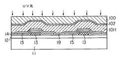
図1は、この発明に係る薄膜トランジスタの構造の一例を概略的に示す断面図である。
【0016】
図1に示したように、この実施の形態に係る薄膜トランジスタ、すなわちCMOS型のTFTは、n型TFT1aと、p型TFT1bとを有している。
これらのTFT1a、1bは、絶縁性基板、例えばガラス基板11上に成膜された絶縁膜としての窒化シリコン膜12上に形成されている。それぞれのTFT1a、1bは、窒化シリコン膜12上に略台形型の島状にパターニングされた例えば膜厚300nmのビスマス・サーメット13、このビスマスサーメット13及びガラス基板11を被覆する例えば膜厚100nmの絶縁膜としての酸化シリコン膜14、及びこの酸化シリコン膜14上に形成された例えば膜厚50nmの多結晶シリコン膜15を有している。
【0017】
ビスマス・サーメット13は、遮光性が良好であるとともに、導電性が少なく、ガラス基板11の裏面側から活性領域20に光が照射されることを防止する機能を有している。
【0018】
多結晶シリコン膜15は、ビスマス・サーメット13のほぼ直上に位置する活性領域20、及びこの活性領域20の両側に位置する伝導領域を含んでいる。n型TFT1aにおける伝導領域は、活性領域20の両端に位置するとともに不純物となるイオンが低濃度でドープされた層、すなわち低濃度領域(以下、LDDと称する)16と、このLDD16の両端に位置するとともにLDD16と同一の不純物が高濃度でドープされた層、すなわち高濃度領域17とを有している。また、p型TFT1bにおける伝導領域は、n型TFT1aにおける高濃度領域17とほぼ同一の不純物濃度のドープ層、すなわち高濃度領域18からなっている。
【0019】
この多結晶シリコン膜15は、図1に示したように、酸化シリコン膜14を介して、島状にパターニングされたビスマス・サーメット13を跨ぐように形成されている。つまり、ビスマス・サーメット13は、略平坦に成膜された窒化シリコン膜12から突出して形成されている。ビスマス・サーメット13の側面は、窒化シリコン膜に対して急峻な角度を成す、すなわちガラス基板の法線に対して小さな角度で傾斜するように形成されている。
【0020】
そして、多結晶シリコン膜15は、ビスマス・サーメット13の略直上からその側面、及び窒化シリコン膜12の直上に至るまで形成されている。
多結晶シリコン膜15におけるビスマス・サーメット13の略直上には、活性領域20が形成され、ビスマス・サーメット13の側面の略直上には、LDD16が形成され、そして、窒化シリコン膜12の略直上には、高濃度領域17、18が形成されている。
【0021】
これらの伝導領域は、活性領域20を挟んで一方がソース領域、他方がドレイン領域として機能する。そして、この多結晶シリコン膜15は、ゲート絶縁膜19によって被覆されている。このゲート絶縁膜19は、例えば酸化シリコンによって形成され、その好適な膜厚は約100nm以下であり、CVD法を用いて形成される。
【0022】
ゲート絶縁膜19上における活性領域20のほぼ直上には、ゲート電極101が形成されている。このゲート電極101は、例えばモリブデン(Mo)及びタングステン(W)の合金からなる金属膜によって形成され、その膜厚は、例えば250nmである。このゲート電極101は、酸化シリコンによって形成された絶縁膜103によって覆われている。
【0023】
また、多結晶シリコン膜15における高濃度領域17は、アルミニウム電極104にコンタクトされ、ソース領域にコンタクトされたアルミニウム電極がソース電極として機能し、ドレイン領域にコンタクトされたアルミニウム電極がドレイン電極として機能する。
【0024】
次に、図1に示したような構造のTFTを製造する製造方法について図2乃至図12を参照して説明する。
まず、図2に示すように、大型のガラス基板11上に、プラズマCVD法により窒化シリコン膜12を成膜した後、スパッタ法を用いてビスマス・サーメット13を300nmの膜厚で成膜する。その後、写真食刻法により、ビスマス・サーメット13上に所定パターンのフォトレジストを形成した後、反応性イオンエッチング法によりビスマス・サーメット13を島状にパターニングする。この時、島状に形成されたビスマス・サーメット13の側壁は、ガラス基板11に対して、急峻な角度で形成され、その角度は、例えば、ガラス基板11に対して80度である。
【0025】
続いて、図3に示すように、プラズマCVD法により、窒化シリコン膜12上、及びビスマス・サーメット13上に、酸化シリコン膜14を100nmの膜厚で成膜する。そして、この酸化シリコン膜14上にアモルファスシリコン115を成膜した後、エキシマレーザを照射してアニールすることにより、多結晶シリコン膜を形成する。この時、多結晶シリコン膜は、窒化シリコン膜12上に突出して形成されたビスマス・サーメット13の形状に倣うように形成されている。
【0026】
続いて、図4に示すように、多結晶シリコン膜15における活性領域及び伝導領域に相当する部分上をフォトレジストで覆った後、化学ドライエッチング法、すなわちCDE法により、この多結晶シリコン膜15をエッチングする。そして、多結晶シリコン膜15を覆っていたフォトレジストを除去した後、ECR(電子サイクロトロン共鳴)プラズマCVD法により、酸化シリコン膜19を100nmの膜厚で成膜する。
【0027】
続いて、図5に示すように、スパッタ法により、酸化シリコン膜19上に、モリブデン及びタングステンの合金1011を250nmの膜厚で形成する。そして、この合金1011の表面にアルミニウム102を50nm程度の膜厚で被着する。そして、ネガ型のフォトレジスト100をアルミニウム102の全面に塗布した後、全面を紫外線光により露光する。この時、低粘度のフォトレジスト100を用いて平坦化を行った後に全面露光を行うと、凸部、すなわち島状のビスマス・サーメット13が形成されている略直上に位置するフォトレジスト100が強く硬化する。
【0028】
そして、この状態で現像すると、図6に示すように、凸部の上に位置するフォトレジスト100のみが残る(d)。
そして、図7に示すように、このフォトレジスト100が残った状態でアルミニウム102及びモリブデン−タングステン合金1011をCDE法によってエッチングして除去した後に、残っているフォトレジスト100を剥離することにより、ゲート電極101が形成される。さらに、ゲート電極101の表面に成膜されているアルミニウム102をエッチングで除去する。
【0029】
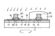
続いて、図8に示すように、p型TFTを形成するべき領域をフォトレジスト110で被覆し、n型TFTを形成するべき領域に不純物を導入するため、イオンドーピング法を用いて不純物、すなわちイオンを注入する。まず、ガラス基板11に対して垂直な方向、すなわちガラス基板11の法線に平行な方向からイオンを入射し、酸化シリコン膜19を介して多結晶シリコン膜15におけるソース領域及びドレイン領域17に不純物を注入する。n型のTFTを形成する場合には、例えば、ホスフィンガス(PH3 )を原料ガスとして用いたイオンを不純物として使用する。イオン注入量は、例えば5×10¹⁵/cm2 であり、加速電圧は、例えば60kVでイオン注入を行う。この工程では、ガラス基板11の法線方向からイオンを入射させるため、ガラス基板11に沿って平坦に形成された多結晶シリコン膜15に対して積極的にイオンを注入している。多結晶シリコン膜15において、ゲート電極101の直下に位置しているために、ほとんどイオンの注入を受けない領域は、活性領域20として機能する。
【0030】
続いて、図9に示すように、イオンの入射角を換え、ビスマス・サーメット13の側面の法線に略平行な方向、例えば、ガラス基板11の法線に対して20度傾けた方向から、再度同一のイオンを注入する。このときの加速電圧は、例えば100kVであり、イオン注入量は、例えば7×10¹³/cm2 である。この工程では、ビスマス・サーメット13の側面に沿って形成された多結晶シリコン膜15に対して積極的にイオンを注入するとともに、イオン注入量を上述した工程より少なくすることにより、LDD16を形成している。この時、ガラス基板側をガラス基板の法線を中心として回転させて、イオンを注入している。
【0031】
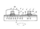
その後、アッシング法によりp型TFTを形成すべき領域を覆っているフォトレジスト110を剥離する。
続いて、図10に示すように、n型TFTを形成するべき領域をフォトレジスト111で被覆し、p型TFTを形成すべき領域に不純物を注入する。p型のTFTを形成する場合には、例えば、ジボラン(B2 H6 )を原料ガスとして用いたイオンを不純物として使用する。この工程では、イオンの入射角は、多結晶シリコン膜のガラス基板に対して平行に形成された平坦部分と、ビスマス・サーメット13の側面に沿って形成された傾斜部分とのなす角の略中間となる角度が選択される。このようなイオン入射角度を選択することにより、一度のイオン注入工程で多結晶シリコン膜の平坦部分と傾斜部分とに略均一な不純物濃度の領域を形成することができる。この実施の形態では、イオンの入射角は、例えば、ガラス基板11の法線方向から20度傾けた方向が選択されている。このときの加速電圧は、例えば70kVであり、イオン注入量は、例えば1×10¹⁶/cm2 である。なお、この工程でも、ガラス基板側をガラス基板の法線を中心として回転させて、イオンを注入している。このようにして、多結晶シリコン膜に、比較的、不純物濃度が高く、且つ略均一な不純物濃度のソース領域及びドレイン領域18を形成することができる。多結晶シリコン膜において、ゲート電極101の直下に位置しているためにほとんどイオンの注入を受けない領域は、活性領域20として機能する。
【0032】
その後、アッシング法により、n型TFTを形成すべき領域を覆っているフォトレジスト111を剥離する。
このようにして多結晶シリコン膜に不純物を注入した後、600℃で1時間、窒素雰囲気中に保持して、不純物を活性化させる。
【0033】
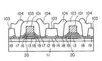
続いて、図11に示すように、CVD法により、酸化シリコン膜103を400nmの膜厚で全面に成膜する。この酸化シリコン膜103は、ゲート電極101の変質を防ぐとともに、多結晶シリコン膜に形成されたソース領域及びドレイン領域への電極を接続する時にソース・ドレイン領域とゲート電極101との短絡を防ぐ役割をなしている。
【0034】
その後、図12に示すように、ソース・ドレイン領域の直上に位置する酸化シリコン膜19及び103にコンタクトホールを開け、アルミニウム104をスパッター法により成膜した後、ソース領域及びドレイン領域にコンタクトしているアルミニウム104のみを電極として残し、エッチングにより除去する。そして、ソース領域にコンタクトしたアルミニウム電極は、ソース電極として機能し、また、ドレイン領域にコンタクトしたアルミニウム電極は、ドレイン電極として機能する。
【0035】
上述したように、図2乃至図12に示したような工程により、TFTの製造が終了する。
このようにして製造されたTFTにおける、多結晶シリコン膜15は、ソース領域及びドレイン領域を有している。そして、このTFTのソース領域及びドレイン領域は、ガラス基板11上の窒化シリコン膜12から突出して形成されたビスマス・サーメット13の略直上に位置する活性領域20と、活性領域20の両側に位置しているとともに窒化シリコン膜12上の酸化シリコン膜14に沿って平坦に形成された平坦部分17と、活性領域及び平坦部分に連続して形成されているとともにビスマス・サーメット13の側面に沿ってガラス基板11に対して傾斜して形成された傾斜部分16とからなる。
【0036】
そして、TFT、特にn型TFTにおいて、傾斜部分16には、平坦部分17より不純物濃度が低い低濃度領域、すなわちLDD16が形成されている。
このLDD16は、多結晶シリコン膜における傾斜部分に形成されるので、不純物としてのイオンをガラス基板11の法線に対してわずかに傾けた角度、好ましくは傾斜部分の斜面の法線方向から注入することによって形成することができる。また、高濃度領域は、多結晶シリコン膜における平坦部分に形成されるので、ガラス基板11の法線方向からイオンを注入することによって形成することができる。
【0037】
したがって、イオン注入量、及び傾斜部分に対するイオン入射角を制御することにより、自己整合的にLDD及び高濃度領域を形成することができる。このため、従来のように、LDDを形成する領域をフォトレジストで覆ってからイオンを注入するといった工程は必要なくなり、製造工程数を削減可能であるとともに、製造コストを低減することが可能となる。また、LDDの長さは、イオン注入する角度、及び多結晶シリコン膜の傾斜部分の傾斜角を適宜好ましい値に選択することにより、制御することが可能となり、加工精度を向上することができる。
【0038】
このようなLDDが活性領域と高濃度領域との間に形成されることにより、n型TFTのドレイン部にかかる電界を緩和し、リーク電流を低減し、電界によるTFT特性の劣化を減らすことができる。
【0039】
ところで、上述した実施の形態では、n型のTFTにおいて、ソース領域とドレイン領域とのそれぞれにLDD16及び高濃度領域17を形成するために、2回のイオン注入工程が必要であったが、ここでは、1回のイオン注入工程でLDD16及び高濃度領域17を形成する方法について説明する。
【0040】
図13には、不純物が入射される角度に対する注入不純物濃度の関係を示す図である。すなわち、不純物としてのイオンを注入する工程では、イオンは、平行に近い軌跡で入射される。このため、イオンを入射させる酸化シリコン膜14への入射角を選ぶと、酸化シリコン膜14の実効的な膜厚が変化し、この酸化シリコン膜14を通過する距離が変化する。すなわち、酸化シリコン膜14に対して垂直な方向、つまり酸化シリコン膜14の法線方向からイオンを入射させた場合に、イオンが通過する酸化シリコン膜14の距離は、酸化シリコン膜14の法線から所定の角度傾けてイオンを入射させた場合にイオンが通過する酸化シリコン膜14の距離より短い。つまり、実効的な膜厚がイオンの入射角度によって異なる。
【0041】
このため、酸化シリコン膜14を通過して多結晶シリコン膜15に到達するイオンの量も異なり、イオン通過距離が短い場合、すなわち酸化シリコン膜14の略垂直方向からイオンを注入した場合は、イオン通過距離が長い場合、すなわち酸化シリコン膜14の法線に対して傾けてイオンを注入した場合より、多くのイオンが注入される。つまり、不純物濃度が高くなる。
【0042】
図13に示したように、酸化シリコン膜14に対して垂直にイオンを注入した場合、多結晶シリコン膜における不純物濃度は、1×10²⁰/cm3 であり、酸化シリコン膜14に対して60度傾いた位置、すなわち酸化シリコン膜14の法線に対して30度傾いた位置からイオンを注した場合、不純物濃度は、1×10¹⁸/cm3 であった。このように、不純物濃度に2桁の差があれば、それぞれLDD及び高濃度領域として十分に機能することが可能である。
【0043】
このように、同一の条件でイオンの入射角度のみを変えることにより、異なる不純物濃度の領域を同時に形成することが可能となる。
そこで、多結晶シリコン膜15の平坦部分は、ガラス基板11に沿って平行に形成し、傾斜部分は、ガラス基板11に対して60度の角度、すなわちガラス基板の法線に対して30度となるように形成する。そして、ガラス基板の法線方向からイオンを注入する。これにより、同一のイオン注入工程で、平坦部分には、1×10²⁰/cm3 の不純物濃度の高濃度領域17が形成され、傾斜部分には、1×10¹⁸/cm3 の不純物濃度のLDD16が同時に形成できる。
【0044】
この方式では、n型TFTのソース領域及びドレイン領域にイオンを注入する過程において、イオンを入射させる入射角、及び多結晶シリコン膜の傾斜部分の角度を適宜選択することにより、1度のイオン注入工程で高濃度領域と、低濃度領域(LDD)を同時に形成することができる。
【0045】
このため、図9に示したような2回目のイオン注入工程が不要となり、さらに製造工程数を削減することが可能となる。
また、上述した実施の形態では、ゲート電極としてモリブデン−タングステンの合金を使用したが、図14に示すように、多結晶シリコン41によって形成されてもよい。この場合、ゲート電極をパターニングする際に、多結晶シリコン膜41上にポジ型のフォトレジスト42を塗布した後、ガラス基板11の裏面から光を入射させて露光する。このようにすることで、ビスマス・サーメット13がマスクとなる。露光されたフォトレジスト42が除去された後、エッチングすることにより、図15に示すように、ビスマス・サーメット13と略同じ大きさのゲート電極41を自己整合的に形成することができる。
【0046】
上述したように、この薄膜トランジスタ及びこの薄膜トランジスタの製造方法によれば、従来では困難であったLDD構造を精度良く作製することが可能となる。また、電極形成のためのレジストパターン形成のために必要なマスク合わせ工程が減り、製造コストを低減するのに有用である。さらに、LDD構造を精度良く形成することが可能となり、駆動能力の大きく、信頼性の高いTFTを提供することができる。
【0047】
【発明の効果】
以上説明したように、この発明によれば、超微細領域をエッチング技術を使わず自己整合的に形成することにより、製造コストの低減が可能であるとともに、加工精度を向上できる薄膜トランジスタ及びこの薄膜トランジスタの製造方法を提供することができる。
【図面の簡単な説明】
【図1】図1は、この発明に係る薄膜トランジスタの構造の一例を概略的に示す断面図である。
【図2】図2は、この発明に係る薄膜トランジスタの製造方法の一工程を示す図である。
【図3】図3は、この発明に係る薄膜トランジスタの製造方法の一工程を示す図である。
【図4】図4は、この発明に係る薄膜トランジスタの製造方法の一工程を示す図である。
【図5】図5は、この発明に係る薄膜トランジスタの製造方法の一工程を示す図である。
【図6】図6は、この発明に係る薄膜トランジスタの製造方法の一工程を示す図である。
【図7】図7は、この発明に係る薄膜トランジスタの製造方法の一工程を示す図である。
【図8】図8は、この発明に係る薄膜トランジスタの製造方法の一工程を示す図である。
【図9】図9は、この発明に係る薄膜トランジスタの製造方法の一工程を示す図である。
【図10】図10は、この発明に係る薄膜トランジスタの製造方法の一工程を示す図である。
【図11】図11は、この発明に係る薄膜トランジスタの製造方法の一工程を示す図である。
【図12】図12は、この発明に係る薄膜トランジスタの製造方法の一工程を示す図である。
【図13】図13は、不純物が入射される角度に対する注入不純物濃度の関係を示す図である。
【図14】図14は、ゲート電極として多結晶シリコンを使用した構造の薄膜トランジスタを製造する一工程を示す図である。
【図15】図15は、ゲート電極として多結晶シリコンを使用した構造の薄膜トランジスタを製造する一工程を示す図である。
【図16】図16は、従来の薄膜トランジスタの構造の一例を示す図である。
【符号の説明】
11…ガラス基板
12…窒化シリコン膜
13…ビスマス・サーメット
14…酸化シリコン膜
15…多結晶シリコン膜
16…低濃度領域
17…高濃度領域
18…p型高濃度領域
19…酸化シリコン膜
101…ゲート電極
103…酸化シリコン膜
104…Al電極
41…多結晶シリコン[0001]
BACKGROUND OF THE INVENTION
The present invention relates to a thin film transistor used for driving a liquid crystal display device and a method of manufacturing the thin film transistor.
[0002]
[Prior art]
In recent years, polycrystalline silicon and amorphous silicon, that is, amorphous silicon, can be formed on a transparent substrate by a CVD (Chemical Vapor Deposition) method or the like, so that a thin film transistor (Thin Film Transistor) that drives a liquid crystal display device is described below. (Hereinafter referred to as “TFT”).
[0003]
A TFT using amorphous silicon as an active layer is used as a switching element for driving a display unit of a liquid crystal display device for each pixel. However, since amorphous silicon has a low carrier mobility, that is, a response speed, it is difficult to apply it to a drive circuit for driving a switching element for each pixel. The circuit cannot be integrally formed. For this reason, there exists a problem that size reduction of a liquid crystal display device is difficult.
[0004]
Therefore, a liquid crystal display device using a TFT using polycrystalline silicon having a higher mobility than amorphous silicon as an active layer has been developed. This TFT using polycrystalline silicon can be applied not only to a switching element for each pixel but also to a drive circuit (mainly composed of CMOS transistors) for operating the switching element. The liquid crystal display device can be miniaturized.
[0005]
However, polycrystalline silicon has the following problems.
The first problem is that due to the high mobility, the avalanche multiplication effect is large, the drain current multiplication phenomenon easily occurs with the voltage between the source and drain, the drain current flows greatly, and the TFT characteristics deteriorate. It is a point to let. The second problem is that a leak current flows when the TFT is turned off through many defects existing inside the polysilicon when irradiated with light. In response to this, attempts have been made to reduce defects by inactivating them with H, but the leakage current cannot be reduced sufficiently.
[0006]
In order to solve these problems, a TFT having a structure as shown in FIG. 16 has been proposed. That is, this TFT has an n-type TFT 5a and a p-
[0007]
In the TFT having such a structure, first, impurities are uniformly implanted into the semiconductor layer patterned on the undercoat layer on the glass substrate, and then the region for forming the LDD is covered with a photoresist, and the impurities are again covered. By implanting, a high concentration region and LDD are formed.
[0008]
[Problems to be solved by the invention]
In the method as described above, a step of covering the semiconductor layer in the region where the LDD is formed with a photoresist is necessary. That is, after implanting impurities into the semiconductor layer, a photoresist is formed on the entire surface and exposed through a mask. Then, by developing the photoresist, the photoresist is left only in the region where the LDD is to be formed, and impurities are implanted again. Then, the remaining photoresist is removed to form an LDD and a high concentration region.
[0009]
Thus, in order to form LDD, the process of patterning a photoresist is required, and the manufacturing process is complicated and the cost increases.
[0010]
Further, the LDD formation accuracy depends on the photoresist formation accuracy. Therefore, strict alignment accuracy of the mask used when exposing the photoresist is required. It is difficult to form a short LDD of 2 μm or less because of the accuracy of the exposure apparatus that exposes the photoresist and the accuracy of the mask.
[0011]
Thus, there arises a problem that it is difficult to control the length of the LDD in terms of processing accuracy.
The present invention has been made in view of the above-described circumstances, and by forming the ultrafine region in a self-aligned manner without using an etching technique, the manufacturing cost can be reduced and the thin film transistor capable of improving the processing accuracy Another object of the present invention is to provide a method for manufacturing the thin film transistor.
[0012]
[Means for Solving the Problems]
The present invention has been made based on the above problems,
According to the invention of
A second flat part formed to protrude from the first flat part and formed at a predetermined height from the first flat part formed of an insulator, and the first flat part and the second flat part. Patterning a protrusion having a side wall connecting the portion;
Covering the first flat portion of the insulator and the protrusion with a first insulating film;
Depositing a polycrystalline silicon film on the second flat portion of the protrusion, the side wall portion, and the first flat portion of the insulator through the first insulating film;
Covering the polycrystalline silicon film with a second insulating film;
Patterning a conductive film substantially directly on the second flat portion through the second insulating film;
Impurities are incident from the normal direction of the first flat portion of the insulator to form a first impurity region in the polycrystalline silicon film located almost immediately above the first flat portion, and a side wall portion of the protrusion Forming a second impurity region having a concentration lower than that of the first impurity region in the polycrystalline silicon film positioned substantially immediately above the first impurity region;
A method for manufacturing a thin film transistor is provided.
[0013]
Claim2According to the invention described in
A second flat part formed to protrude from the first flat part and formed at a predetermined height from the first flat part formed of an insulator, and the first flat part and the second flat part. Patterning a protrusion having a side wall connecting the portion;
Covering the first flat portion of the insulator and the protrusion with a first insulating film;
Depositing a polycrystalline silicon film on the second flat portion of the protrusion, the side wall portion, and the first flat portion of the insulator through the first insulating film;
Covering the polycrystalline silicon film with a second insulating film;
Patterning a conductive film substantially directly on the second flat portion through the second insulating film;
covering the polycrystalline silicon film and the conductive film at a position where a p-type thin film transistor is to be formed with a resist;
A step of making an impurity enter from a normal direction of the first flat portion of the insulator, and forming a first impurity region in the polycrystalline silicon film positioned substantially immediately above the first flat portion;
A step of making an impurity enter from a normal direction of the side wall portion of the protrusion, and forming a second impurity region having a lower concentration than the first impurity region in the polycrystalline silicon film positioned substantially immediately above the side wall portion;
Removing the resist;
covering the polycrystalline silicon film in which the first and second impurity regions at positions where an n-type thin film transistor is to be formed and the conductive film are covered with a resist;
A step of making an impurity enter from a position substantially in the middle of the angle formed by the first flat portion and the side wall portion to form an impurity region having a substantially uniform concentration in the polycrystalline silicon film;
Removing the resist;
A method for manufacturing a thin film transistor is provided.
[0015]
DETAILED DESCRIPTION OF THE INVENTION
Embodiments of a thin film transistor and a method of manufacturing the thin film transistor according to the present invention will be described below with reference to the drawings.
FIG. 1 is a sectional view schematically showing an example of the structure of a thin film transistor according to the present invention.
[0016]
As shown in FIG. 1, the thin film transistor according to this embodiment, that is, a CMOS type TFT has an n type TFT 1a and a p type TFT 1b.
These TFTs 1 a and 1 b are formed on a
[0017]
The
[0018]
The
[0019]
As shown in FIG. 1, the
[0020]
The
In the
[0021]
One of these conductive regions functions as a source region and the other functions as a drain region across the
[0022]
A
[0023]
The
[0024]
Next, a manufacturing method for manufacturing the TFT having the structure as shown in FIG. 1 will be described with reference to FIGS.
First, as shown in FIG. 2, after a
[0025]
Subsequently, as shown in FIG. 3, a
[0026]
Subsequently, as shown in FIG. 4, after the portions corresponding to the active region and the conductive region in the
[0027]
Subsequently, as shown in FIG. 5, an
[0028]
When developing in this state, as shown in FIG. 6, only the
Then, as shown in FIG. 7, the
[0029]
Subsequently, as shown in FIG. 8, the region where the p-type TFT is to be formed is covered with a
[0030]
Subsequently, as shown in FIG. 9, the incident angle of the ions is changed, and from a direction substantially parallel to the normal line of the side surface of the
[0031]
Thereafter, the
Subsequently, as shown in FIG. 10, the region where the n-type TFT is to be formed is covered with a photoresist 111, and impurities are implanted into the region where the p-type TFT is to be formed. When forming a p-type TFT, for example, diborane (B2 H6 ) Is used as an impurity. In this step, the incident angle of ions is approximately the middle of the angle formed between the flat portion formed parallel to the glass substrate of the polycrystalline silicon film and the inclined portion formed along the side surface of the
[0032]
Thereafter, the photoresist 111 covering the region where the n-type TFT is to be formed is removed by ashing.
After the impurities are implanted into the polycrystalline silicon film in this manner, the impurities are activated by holding in a nitrogen atmosphere at 600 ° C. for 1 hour.
[0033]
Subsequently, as shown in FIG. 11, a
[0034]
Thereafter, as shown in FIG. 12, contact holes are opened in the
[0035]
As described above, the manufacturing of the TFT is completed through the processes shown in FIGS.
The
[0036]
In the TFT, in particular, the n-type TFT, a low concentration region having a lower impurity concentration than the
Since this
[0037]
Therefore, the LDD and the high concentration region can be formed in a self-aligned manner by controlling the ion implantation amount and the ion incident angle with respect to the inclined portion. For this reason, unlike the conventional method, the step of covering the region where the LDD is formed with a photoresist and then implanting ions is not necessary, and the number of manufacturing steps can be reduced and the manufacturing cost can be reduced. . Further, the length of the LDD can be controlled by appropriately selecting the ion implantation angle and the inclination angle of the inclined portion of the polycrystalline silicon film, and the processing accuracy can be improved.
[0038]
By forming such an LDD between the active region and the high concentration region, the electric field applied to the drain portion of the n-type TFT can be relaxed, the leakage current can be reduced, and the deterioration of TFT characteristics due to the electric field can be reduced. it can.
[0039]
Incidentally, in the above-described embodiment, in order to form the
[0040]
FIG. 13 is a diagram showing the relationship of the implanted impurity concentration with respect to the angle at which impurities are incident. That is, in the step of implanting ions as impurities, the ions are incident with a locus close to parallel. Therefore, when the incident angle to the
[0041]
For this reason, the amount of ions passing through the
[0042]
As shown in FIG. 13, when ions are implanted perpendicular to the
[0043]
Thus, by changing only the incident angle of ions under the same conditions, regions having different impurity concentrations can be formed simultaneously.
Therefore, the flat portion of the
[0044]
In this method, in the process of implanting ions into the source region and the drain region of the n-type TFT, an ion incident angle and an angle of an inclined portion of the polycrystalline silicon film are appropriately selected to perform ion implantation once. A high concentration region and a low concentration region (LDD) can be formed simultaneously in the process.
[0045]
For this reason, the second ion implantation step as shown in FIG. 9 is not required, and the number of manufacturing steps can be further reduced.
Further, in the above-described embodiment, a molybdenum-tungsten alloy is used as the gate electrode, but it may be formed of
[0046]
As described above, according to the thin film transistor and the method for manufacturing the thin film transistor, an LDD structure, which has been difficult in the past, can be accurately manufactured. In addition, the mask alignment process necessary for forming a resist pattern for electrode formation is reduced, which is useful for reducing the manufacturing cost. Further, the LDD structure can be formed with high accuracy, and a TFT with high driving capability and high reliability can be provided.
[0047]
【The invention's effect】
As described above, according to the present invention, the ultrafine region is formed in a self-aligned manner without using an etching technique, so that the manufacturing cost can be reduced and the processing accuracy can be improved. A manufacturing method can be provided.
[Brief description of the drawings]
FIG. 1 is a cross-sectional view schematically showing an example of the structure of a thin film transistor according to the present invention.
FIG. 2 is a diagram showing one step in a method of manufacturing a thin film transistor according to the present invention.
FIG. 3 is a diagram showing one step in a method of manufacturing a thin film transistor according to the present invention.
FIG. 4 is a diagram showing one step in a method of manufacturing a thin film transistor according to the present invention.
FIG. 5 is a diagram showing one step in a method of manufacturing a thin film transistor according to the present invention.
FIG. 6 is a diagram showing one step in a method of manufacturing a thin film transistor according to the present invention.
FIG. 7 is a diagram showing one step in a method of manufacturing a thin film transistor according to the present invention.
FIG. 8 is a diagram showing one step in a method of manufacturing a thin film transistor according to the present invention.
FIG. 9 is a diagram showing one step in a method for manufacturing a thin film transistor according to the present invention.
FIG. 10 is a diagram showing a step in a method of manufacturing a thin film transistor according to the present invention.
FIG. 11 is a diagram showing one step in a method of manufacturing a thin film transistor according to the present invention.
FIG. 12 is a diagram showing a step in the method of manufacturing a thin film transistor according to the present invention.
FIG. 13 is a diagram showing a relationship of an implanted impurity concentration with respect to an angle at which an impurity is incident.
FIG. 14 is a diagram showing a process of manufacturing a thin film transistor having a structure using polycrystalline silicon as a gate electrode.
FIG. 15 is a diagram showing a process of manufacturing a thin film transistor having a structure using polycrystalline silicon as a gate electrode.
FIG. 16 is a diagram showing an example of a structure of a conventional thin film transistor.
[Explanation of symbols]
11 ... Glass substrate
12 ... Silicon nitride film
13 ... Bismuth Cermet
14 ... Silicon oxide film
15 ... polycrystalline silicon film
16: Low concentration region
17 ... High concentration region
18 ... p-type high concentration region
19 ... Silicon oxide film
101 ... Gate electrode
103 ... Silicon oxide film
104 ... Al electrode
41 ... polycrystalline silicon
Claims (2)
Translated fromJapanese前記絶縁体の第1平坦部及び前記突起部を第1絶縁膜で覆う工程と、
前記第1絶縁膜を介して前記突起部の第2平坦部、側壁部、及び前記絶縁体の第1平坦部の略直上に多結晶シリコン膜を成膜する工程と、
前記多結晶シリコン膜を第2絶縁膜で覆う工程と、
前記第2絶縁膜を介して前記第2平坦部の略直上に導電膜をパターニングする工程と、
前記絶縁体の第1平坦部の法線方向から不純物を入射させ、前記第1平坦部の略直上に位置する前記多結晶シリコン膜に第1不純物領域を形成するとともに、前記突起部の側壁部の略直上に位置する前記多結晶シリコン膜に前記第1不純物領域より低濃度の第2不純物領域を形成する工程と、
を有することを特徴とする薄膜トランジスタの製造方法。A second flat part formed to protrude from the first flat part at a predetermined height, and the first flat part and the second flat part. Patterning a protrusion having a side wall connecting the portion;
Covering the first flat portion of the insulator and the protrusion with a first insulating film;
Depositing a polycrystalline silicon film on the second flat portion of the protrusion, the side wall portion, and the first flat portion of the insulator through the first insulating film;
Covering the polycrystalline silicon film with a second insulating film;
Patterning a conductive film substantially directly on the second flat portion through the second insulating film;
Impurities are incident from the normal direction of the first flat portion of the insulator to form a first impurity region in the polycrystalline silicon film located substantially immediately above the first flat portion, and a side wall portion of the protrusion Forming a second impurity region having a concentration lower than that of the first impurity region in the polycrystalline silicon film positioned substantially immediately above the first impurity region;
A method for producing a thin film transistor, comprising:
前記絶縁体の第1平坦部及び前記突起部を第1絶縁膜で覆う工程と、
前記第1絶縁膜を介して前記突起部の第2平坦部、側壁部、及び前記絶縁体の第1平坦部の略直上に多結晶シリコン膜を成膜する工程と、
前記多結晶シリコン膜を第2絶縁膜で覆う工程と、
前記第2絶縁膜を介して前記第2平坦部の略直上に導電膜をパターニングする工程と、
p型薄膜トランジスタを形成するべき位置の前記多結晶シリコン膜及び前記導電膜をレジストで覆う工程と、
前記絶縁体の第1平坦部の法線方向から不純物を入射させ、前記第1平坦部の略直上に位置する前記多結晶シリコン膜に第1不純物領域を形成する工程と、
前記突起部の側壁部の法線方向から不純物を入射させ、前記側壁部の略直上に位置する前記多結晶シリコン膜に前記第1不純物領域より低濃度の第2不純物領域を形成する工程と、
前記レジストを除去する工程と、
n型薄膜トランジスタを形成するべき位置の前記第1及び第2不純物領域が形成された多結晶シリコン膜と前記導電膜とをレジストで覆う工程と、
前記第1平坦部と前記側壁部とのなす角の略中間の位置から不純物を入射させ、多結晶シリコン膜に略均一な濃度の不純物領域を形成する工程と、
前記レジストを除去する工程と
を有することを特徴とする薄膜トランジスタの製造方法。A second flat part formed to protrude from the first flat part at a predetermined height, and the first flat part and the second flat part. Patterning a protrusion having a side wall connecting the portion;
Covering the first flat portion of the insulator and the protrusion with a first insulating film;
Depositing a polycrystalline silicon film on the second flat portion of the protrusion, the side wall portion, and the first flat portion of the insulator through the first insulating film;
Covering the polycrystalline silicon film with a second insulating film;
Patterning a conductive film substantially directly on the second flat portion through the second insulating film;
covering the polycrystalline silicon film and the conductive film at a position where a p-type thin film transistor is to be formed with a resist;
A step of making an impurity enter from a normal direction of the first flat portion of the insulator, and forming a first impurity region in the polycrystalline silicon film positioned substantially immediately above the first flat portion;
A step of making an impurity enter from a normal direction of the side wall portion of the protrusion, and forming a second impurity region having a lower concentration than the first impurity region in the polycrystalline silicon film positioned substantially immediately above the side wall portion;
Removing the resist;
covering the polycrystalline silicon film in which the first and second impurity regions at positions where an n-type thin film transistor is to be formed and the conductive film are covered with a resist;
A step of making an impurity enter from a position substantially in the middle of the angle formed by the first flat portion and the side wall portion to form an impurity region having a substantially uniform concentration in the polycrystalline silicon film;
And a step of removing the resist.
Priority Applications (1)
| Application Number | Priority Date | Filing Date | Title |
|---|---|---|---|
| JP15121297AJP3923600B2 (en) | 1997-06-09 | 1997-06-09 | Thin film transistor manufacturing method |
Applications Claiming Priority (1)
| Application Number | Priority Date | Filing Date | Title |
|---|---|---|---|
| JP15121297AJP3923600B2 (en) | 1997-06-09 | 1997-06-09 | Thin film transistor manufacturing method |
Publications (2)
| Publication Number | Publication Date |
|---|---|
| JPH10341020A JPH10341020A (en) | 1998-12-22 |
| JP3923600B2true JP3923600B2 (en) | 2007-06-06 |
Family
ID=15513695
Family Applications (1)
| Application Number | Title | Priority Date | Filing Date |
|---|---|---|---|
| JP15121297AExpired - Fee RelatedJP3923600B2 (en) | 1997-06-09 | 1997-06-09 | Thin film transistor manufacturing method |
Country Status (1)
| Country | Link |
|---|---|
| JP (1) | JP3923600B2 (en) |
Families Citing this family (3)
| Publication number | Priority date | Publication date | Assignee | Title |
|---|---|---|---|---|
| TW490713B (en) | 1999-07-22 | 2002-06-11 | Semiconductor Energy Lab | Semiconductor device and manufacturing method thereof |
| JP4776773B2 (en)* | 1999-12-10 | 2011-09-21 | 株式会社半導体エネルギー研究所 | Method for manufacturing semiconductor device |
| KR101983691B1 (en) | 2012-08-17 | 2019-05-30 | 삼성디스플레이 주식회사 | Light blocking member and display panel including the same |
- 1997
- 1997-06-09JPJP15121297Apatent/JP3923600B2/ennot_activeExpired - Fee Related
Also Published As
| Publication number | Publication date |
|---|---|
| JPH10341020A (en) | 1998-12-22 |
Similar Documents
| Publication | Publication Date | Title |
|---|---|---|
| US5010027A (en) | Method for fabricating a self-aligned thin-film transistor utilizing planarization and back-side photoresist exposure | |
| JP3398453B2 (en) | Method for manufacturing thin film transistor | |
| JP4037117B2 (en) | Display device | |
| US6440784B2 (en) | Thin film transistor and a fabricating method thereof | |
| US5658808A (en) | Method of fabricating polycrystalline silicon thin-film transistor having symmetrical lateral resistors | |
| KR19980016968A (en) | Self-aligned thin film transistor manufacturing method | |
| KR100330165B1 (en) | A manufacturing method of a thin film transistor liquid crystal display | |
| JP3296975B2 (en) | Thin film transistor and method of manufacturing the same | |
| JP2004040108A (en) | Thin film transistor having LDD structure and method of manufacturing the same | |
| US6475843B2 (en) | Polysilicon thin film transistor with a self-aligned LDD structure | |
| JP3923600B2 (en) | Thin film transistor manufacturing method | |
| JPH07211912A (en) | Thin film transistor and its manufacture | |
| JP3528422B2 (en) | Method for manufacturing thin film transistor | |
| JP3420301B2 (en) | Method for manufacturing thin film transistor | |
| JP3210196B2 (en) | Thin film transistor and manufacturing method thereof | |
| JPH05152325A (en) | Manufacturing method of thin film transistor | |
| JP3358284B2 (en) | Method for manufacturing thin film transistor | |
| JP2595757B2 (en) | Thin film field effect transistor and method of manufacturing the same | |
| JP4160174B2 (en) | Semiconductor device | |
| KR100498629B1 (en) | Manufacturing method of liquid crystal display device | |
| KR100304911B1 (en) | Thin Film Transistor Manufacturing Method | |
| JP2630195B2 (en) | Thin film field effect transistor and method of manufacturing the same | |
| JPH09326495A (en) | Thin film transistor and manufacturing method thereof | |
| JP2716035B2 (en) | Thin film field effect transistor | |
| KR970003742B1 (en) | Self-aligned thin film transistor manufacturing method |
Legal Events
| Date | Code | Title | Description |
|---|---|---|---|
| A621 | Written request for application examination | Free format text:JAPANESE INTERMEDIATE CODE: A621 Effective date:20040609 | |
| A977 | Report on retrieval | Free format text:JAPANESE INTERMEDIATE CODE: A971007 Effective date:20060529 | |
| A131 | Notification of reasons for refusal | Free format text:JAPANESE INTERMEDIATE CODE: A131 Effective date:20060606 | |
| A521 | Written amendment | Free format text:JAPANESE INTERMEDIATE CODE: A523 Effective date:20060726 | |
| TRDD | Decision of grant or rejection written | ||
| A01 | Written decision to grant a patent or to grant a registration (utility model) | Free format text:JAPANESE INTERMEDIATE CODE: A01 Effective date:20070220 | |
| A61 | First payment of annual fees (during grant procedure) | Free format text:JAPANESE INTERMEDIATE CODE: A61 Effective date:20070222 | |
| FPAY | Renewal fee payment (prs date is renewal date of database) | Free format text:PAYMENT UNTIL: 20100302 Year of fee payment:3 | |
| S111 | Request for change of ownership or part of ownership | Free format text:JAPANESE INTERMEDIATE CODE: R313113 | |
| FPAY | Renewal fee payment (prs date is renewal date of database) | Free format text:PAYMENT UNTIL: 20100302 Year of fee payment:3 | |
| R350 | Written notification of registration of transfer | Free format text:JAPANESE INTERMEDIATE CODE: R350 | |
| LAPS | Cancellation because of no payment of annual fees |