JP3918765B2 - Liquid crystal display device and electronic device - Google Patents
Liquid crystal display device and electronic deviceDownload PDFInfo
- Publication number
- JP3918765B2 JP3918765B2JP2003116365AJP2003116365AJP3918765B2JP 3918765 B2JP3918765 B2JP 3918765B2JP 2003116365 AJP2003116365 AJP 2003116365AJP 2003116365 AJP2003116365 AJP 2003116365AJP 3918765 B2JP3918765 B2JP 3918765B2
- Authority
- JP
- Japan
- Prior art keywords
- region
- sub
- layer
- liquid crystal
- pixel
- Prior art date
- Legal status (The legal status is an assumption and is not a legal conclusion. Google has not performed a legal analysis and makes no representation as to the accuracy of the status listed.)
- Expired - Lifetime
Links
- 239000004973liquid crystal related substanceSubstances0.000titleclaimsdescription88
- 230000005540biological transmissionEffects0.000claimsdescription56
- 239000000758substrateSubstances0.000claimsdescription40
- 230000002093peripheral effectEffects0.000claimsdescription23
- 239000003086colorantSubstances0.000claimsdescription11
- 239000000049pigmentSubstances0.000claimsdescription7
- 239000010408filmSubstances0.000description22
- 239000011159matrix materialSubstances0.000description7
- 238000012986modificationMethods0.000description7
- 230000004048modificationEffects0.000description7
- 229910052751metalInorganic materials0.000description6
- 239000002184metalSubstances0.000description6
- 230000005684electric fieldEffects0.000description5
- 238000005192partitionMethods0.000description5
- 238000002834transmittanceMethods0.000description5
- 238000011161developmentMethods0.000description4
- 238000004519manufacturing processMethods0.000description4
- 239000004642PolyimideSubstances0.000description3
- 210000002858crystal cellAnatomy0.000description3
- 230000007423decreaseEffects0.000description3
- 238000005286illuminationMethods0.000description3
- 229920001721polyimidePolymers0.000description3
- 239000011347resinSubstances0.000description3
- 229920005989resinPolymers0.000description3
- 229910045601alloyInorganic materials0.000description2
- 239000000956alloySubstances0.000description2
- XAGFODPZIPBFFR-UHFFFAOYSA-NaluminiumChemical compound[Al]XAGFODPZIPBFFR-UHFFFAOYSA-N0.000description2
- 230000007547defectEffects0.000description2
- 230000000694effectsEffects0.000description2
- 239000011521glassSubstances0.000description2
- AMGQUBHHOARCQH-UHFFFAOYSA-Nindium;oxotinChemical compound[In].[Sn]=OAMGQUBHHOARCQH-UHFFFAOYSA-N0.000description2
- 239000000463materialSubstances0.000description2
- 239000004033plasticSubstances0.000description2
- 239000003566sealing materialSubstances0.000description2
- 239000010409thin filmSubstances0.000description2
- 229910000838Al alloyInorganic materials0.000description1
- VYZAMTAEIAYCRO-UHFFFAOYSA-NChromiumChemical compound[Cr]VYZAMTAEIAYCRO-UHFFFAOYSA-N0.000description1
- VYPSYNLAJGMNEJ-UHFFFAOYSA-NSilicium dioxideChemical compoundO=[Si]=OVYPSYNLAJGMNEJ-UHFFFAOYSA-N0.000description1
- 229910001080W alloyInorganic materials0.000description1
- NIXOWILDQLNWCW-UHFFFAOYSA-Nacrylic acid groupChemical groupC(C=C)(=O)ONIXOWILDQLNWCW-UHFFFAOYSA-N0.000description1
- 229910052782aluminiumInorganic materials0.000description1
- 229910052804chromiumInorganic materials0.000description1
- 239000011651chromiumSubstances0.000description1
- 238000013461designMethods0.000description1
- 238000005530etchingMethods0.000description1
- 238000000034methodMethods0.000description1
- 230000003287optical effectEffects0.000description1
- 230000000149penetrating effectEffects0.000description1
- 238000012545processingMethods0.000description1
- 230000002040relaxant effectEffects0.000description1
- 230000000630rising effectEffects0.000description1
- 229910052814silicon oxideInorganic materials0.000description1
- 229910052709silverInorganic materials0.000description1
- 239000004332silverSubstances0.000description1
Images


Classifications
- G—PHYSICS
- G02—OPTICS
- G02F—OPTICAL DEVICES OR ARRANGEMENTS FOR THE CONTROL OF LIGHT BY MODIFICATION OF THE OPTICAL PROPERTIES OF THE MEDIA OF THE ELEMENTS INVOLVED THEREIN; NON-LINEAR OPTICS; FREQUENCY-CHANGING OF LIGHT; OPTICAL LOGIC ELEMENTS; OPTICAL ANALOGUE/DIGITAL CONVERTERS
- G02F1/00—Devices or arrangements for the control of the intensity, colour, phase, polarisation or direction of light arriving from an independent light source, e.g. switching, gating or modulating; Non-linear optics
- G02F1/01—Devices or arrangements for the control of the intensity, colour, phase, polarisation or direction of light arriving from an independent light source, e.g. switching, gating or modulating; Non-linear optics for the control of the intensity, phase, polarisation or colour
- G02F1/13—Devices or arrangements for the control of the intensity, colour, phase, polarisation or direction of light arriving from an independent light source, e.g. switching, gating or modulating; Non-linear optics for the control of the intensity, phase, polarisation or colour based on liquid crystals, e.g. single liquid crystal display cells
- G02F1/133—Constructional arrangements; Operation of liquid crystal cells; Circuit arrangements
- G02F1/1333—Constructional arrangements; Manufacturing methods
- G02F1/1335—Structural association of cells with optical devices, e.g. polarisers or reflectors
- G02F1/133553—Reflecting elements
- G02F1/133555—Transflectors
- B—PERFORMING OPERATIONS; TRANSPORTING
- B32—LAYERED PRODUCTS
- B32B—LAYERED PRODUCTS, i.e. PRODUCTS BUILT-UP OF STRATA OF FLAT OR NON-FLAT, e.g. CELLULAR OR HONEYCOMB, FORM
- B32B11/00—Layered products comprising a layer of bituminous or tarry substances
- B32B11/10—Layered products comprising a layer of bituminous or tarry substances next to a fibrous or filamentary layer
- B—PERFORMING OPERATIONS; TRANSPORTING
- B32—LAYERED PRODUCTS
- B32B—LAYERED PRODUCTS, i.e. PRODUCTS BUILT-UP OF STRATA OF FLAT OR NON-FLAT, e.g. CELLULAR OR HONEYCOMB, FORM
- B32B11/00—Layered products comprising a layer of bituminous or tarry substances
- B32B11/02—Layered products comprising a layer of bituminous or tarry substances with fibres or particles being present as additives in the layer
- B—PERFORMING OPERATIONS; TRANSPORTING
- B32—LAYERED PRODUCTS
- B32B—LAYERED PRODUCTS, i.e. PRODUCTS BUILT-UP OF STRATA OF FLAT OR NON-FLAT, e.g. CELLULAR OR HONEYCOMB, FORM
- B32B5/00—Layered products characterised by the non- homogeneity or physical structure, i.e. comprising a fibrous, filamentary, particulate or foam layer; Layered products characterised by having a layer differing constitutionally or physically in different parts
- B32B5/02—Layered products characterised by the non- homogeneity or physical structure, i.e. comprising a fibrous, filamentary, particulate or foam layer; Layered products characterised by having a layer differing constitutionally or physically in different parts characterised by structural features of a fibrous or filamentary layer
- B32B5/022—Non-woven fabric
- G—PHYSICS
- G02—OPTICS
- G02F—OPTICAL DEVICES OR ARRANGEMENTS FOR THE CONTROL OF LIGHT BY MODIFICATION OF THE OPTICAL PROPERTIES OF THE MEDIA OF THE ELEMENTS INVOLVED THEREIN; NON-LINEAR OPTICS; FREQUENCY-CHANGING OF LIGHT; OPTICAL LOGIC ELEMENTS; OPTICAL ANALOGUE/DIGITAL CONVERTERS
- G02F1/00—Devices or arrangements for the control of the intensity, colour, phase, polarisation or direction of light arriving from an independent light source, e.g. switching, gating or modulating; Non-linear optics
- G02F1/01—Devices or arrangements for the control of the intensity, colour, phase, polarisation or direction of light arriving from an independent light source, e.g. switching, gating or modulating; Non-linear optics for the control of the intensity, phase, polarisation or colour
- G02F1/13—Devices or arrangements for the control of the intensity, colour, phase, polarisation or direction of light arriving from an independent light source, e.g. switching, gating or modulating; Non-linear optics for the control of the intensity, phase, polarisation or colour based on liquid crystals, e.g. single liquid crystal display cells
- G02F1/133—Constructional arrangements; Operation of liquid crystal cells; Circuit arrangements
- G02F1/1333—Constructional arrangements; Manufacturing methods
- G02F1/1335—Structural association of cells with optical devices, e.g. polarisers or reflectors
- G02F1/133509—Filters, e.g. light shielding masks
- G02F1/133514—Colour filters
- B—PERFORMING OPERATIONS; TRANSPORTING
- B32—LAYERED PRODUCTS
- B32B—LAYERED PRODUCTS, i.e. PRODUCTS BUILT-UP OF STRATA OF FLAT OR NON-FLAT, e.g. CELLULAR OR HONEYCOMB, FORM
- B32B2262/00—Composition or structural features of fibres which form a fibrous or filamentary layer or are present as additives
- B32B2262/02—Synthetic macromolecular fibres
- B32B2262/0276—Polyester fibres
- B—PERFORMING OPERATIONS; TRANSPORTING
- B32—LAYERED PRODUCTS
- B32B—LAYERED PRODUCTS, i.e. PRODUCTS BUILT-UP OF STRATA OF FLAT OR NON-FLAT, e.g. CELLULAR OR HONEYCOMB, FORM
- B32B2307/00—Properties of the layers or laminate
- B32B2307/70—Other properties
- B32B2307/726—Permeability to liquids, absorption
- B32B2307/7265—Non-permeable
Landscapes
- Physics & Mathematics (AREA)
- Nonlinear Science (AREA)
- Mathematical Physics (AREA)
- Chemical & Material Sciences (AREA)
- Crystallography & Structural Chemistry (AREA)
- General Physics & Mathematics (AREA)
- Optics & Photonics (AREA)
- Engineering & Computer Science (AREA)
- Textile Engineering (AREA)
- Liquid Crystal (AREA)
- Optical Filters (AREA)
Description
Translated fromJapanese【0001】
【発明の属する技術分野】
本発明は、液晶表示装置および電子機器に関し、特に反射モード、透過モードでの色純度のバランスに優れた半透過反射型の液晶表示装置の構成に関するものである。
【0002】
【従来の技術】
明るい場所では太陽光、照明光等の外光を利用し、暗い場所ではバックライト等の内部光源により表示を可能にした液晶表示装置が提案されている。つまり、この液晶表示装置は、反射型と透過型を兼ね備えた表示方式を採用しており、周囲の明るさに応じて反射モードまたは透過モードのいずれかの表示方式に切り替えることで、消費電力を低減しつつ周囲が暗い場合でも明瞭な表示を行うことができるものである。以下、本明細書では、この種の液晶表示装置のことを「半透過反射型液晶表示装置」という。また近年、携帯型電子機器やOA機器などの発展に伴って、半透過反射型液晶表示装置の分野においても、カラー化が要求される場合が多くなっている。この要求を満足する半透過反射型カラー液晶表示装置として、上基板、下基板のいずれかにカラーフィルターを備えたものが提供されている。この種の液晶表示装置の場合、反射モードにおいては、上基板側から入射した外光が、カラーフィルターを透過した後、反射層で反射され、再度カラーフィルターを透過するようになっている。透過モードにおいては、バックライトから下基板に入射した照明光がカラーフィルターを透過するようになっている。通常の構成では、反射モードでも透過モードでも同一のカラーフィルターを用いて表示が行われる。
【0003】
この液晶表示装置においては、上述したように、反射モード時には2回、透過モード時には1回、入射光がカラーフィルターを透過することによりカラー表示が得られるようになっている。このため、例えばカラーフィルターを2回透過する反射モード時の色を重視して淡い色のカラーフィルターを備えた場合には、カラーフィルターを1回しか透過しない透過モード時に発色の良い表示を得ることが難しい。しかしながら、これとは逆にカラーフィルターを1回透過する透過モード時の色を重視して濃い色のカラーフィルターを備えた場合には、カラーフィルターを2回透過する反射モードの表示が暗くなるため、充分な視認性が得られなくなってしまう。このように、従来の半透過反射型カラー液晶表示装置では、反射モード時にも透過モード時にも同様に発色が良く、視認性の高い表示を得ることは困難であった。
【0004】
上記の問題を解決するために、図11に示す構成の液晶表示装置が提案されている(例えば、特許文献1参照)。この液晶表示装置はアクティブマトリクス型液晶表示装置の例であり、データ線101と走査線102とが互いに交差して配置され、交差点の近傍に薄膜トランジスタ103(Thin Film Transistor, 以下、TFTと略記する)が設けられ、TFT103に接続された画素電極104が設けられている。画素電極104は、AlW(アルミニウム・タングステン合金)等の金属膜からなり、反射モードの表示に係わる反射電極105と、ITO(インジウム錫酸化物)等の透明導電膜からなり、透過モードの表示に係わる透明電極106とから構成されている。反射電極105が透明電極106の周囲を取り囲むように配置されており、画素電極104の中央側が透過領域T、周縁側が反射領域Rとなっている。そして、画素電極104の内側に、画素電極104よりも細い幅のカラーフィルター111A,111B,111Cが設けられており、したがって、透過領域Tは、その全体がカラーフィルター111A,111B,111Cと平面的に重なる一方、反射領域Rは、その一部がカラーフィルター111A,111B,111Cと平面的に重なる着色領域Cとなり、残りはカラーフィルター111A,111B,111Cと平面的に重ならない非着色領域Hとなる。
【0005】
この構成においては、反射モード時に上基板側から入射する光の一部は非着色領域Hを透過することになり、反射モード時にカラーフィルターを2回透過することによって得られる光は、非着色領域Hを透過する着色されない光(白色光)と着色領域Cを透過する着色された光とが重畳されたものとなる。一方、透過モード時にバックライトからの透過領域Tを透過する光は全て着色領域Cを透過することになり、透過モード時にカラーフィルターを1回透過することによって得られる光は全て着色された光となる。このようにして、反射モード時にカラーフィルターを2回透過して得られる光と、透過モード時にカラーフィルターを1回透過して得られる光との色の濃淡差を小さくすることができるので、カラーフィルターの色素層を最適化することで反射モード時にも透過モード時にも発色が良く、視認性の高い表示を得ることができる。
【0006】
【特許文献1】
特開2000−111902号公報
【0007】
【発明が解決しようとする課題】
ところが、上記特許文献1に記載の従来の液晶表示装置において、透過モードの表示では特に問題ないが、反射モードの表示における色純度のバラツキが大きいという問題があった。この色純度バラツキは一つの製品の表示領域内、もしくは複数の製品間で生じる場合があり、半透過反射型カラー液晶表示装置において特に反射モードの表示品位を低下する要因となる。
【0008】
本発明は、上記の課題を解決するためになされたものであって、半透過反射型カラー液晶表示装置において、反射モード時にも透過モード時にも発色が良く、また、色純度のバラツキの少ない液晶表示装置を提供することを目的とする。さらに、本発明は、優れた表示品位を有する上記液晶表示装置を備えた電子機器を提供することを目的とする。
【0009】
【課題を解決するための手段】
上記の目的を達成するために、本発明の液晶表示装置は、反射領域及び透過領域からなり異なる色に対応する複数のサブ画素領域と、互いに対向配置された一対の基板と、前記一対の基板間に狭持された液晶層と、前記液晶層を駆動する一対の電極と、前記反射領域に設けられた反射層と、前記反射層に重なり前記各サブ画素領域に対応して色素層が配列されたカラーフィルターとを有し、前記各サブ画素毎に前記反射領域と前記反射層が存在しない透過領域とで表示を行う半透過反射型の液晶表示装置であって、前記反射領域内に、前記色素層が存在する着色領域と前記色素層が存在しない非着色領域とが設けられ、前記着色領域と前記非着色領域の双方が、前記一対の電極のうち一方の電極における前記サブ画素領域の長手方向に沿う周縁部と重なるように設けられ、前記非着色領域は、前記サブ画素領域の短手方向に当該画素領域を横断するように延在し、前記複数のサブ画素領域のうち隣接するサブ画素同士において、一方のサブ画素における非着色領域が他方のサブ画素における非着色領域に対して短手方向の延長線上の領域に形成されるとともに、各々の非着色領域の面積が異なることを特徴とする。ここで言う「サブ画素領域」とは、複数の異なる色に対応する表示領域でフルカラーの1画素を構成する基本となる1単位領域のことである。
【0010】
[従来の技術]の項で例示したように、反射領域内にカラーフィルターの非着色領域を設けた液晶表示装置は、反射モード、透過モードの双方で発色が良い点で優れたものである一方、色純度のバラツキが大きいという問題を有していた。本発明者らは、その原因を調査した結果、各サブ画素領域の電極の縁部で生じる液晶のディスクリネーション(配向乱れ)が色純度のバラツキの原因の一つとなっていることを突き止めた。すなわち、各サブ画素領域の電極の中央寄りの部分では上下基板間の液晶層内に生じる電界(電気力線)は基板面に垂直な方向に作用するが、電極の周縁部では電界(電気力線)が基板面に対して斜め方向に作用する。さらに、電極の周縁部では隣接する電極との間での横電界も作用する。その結果、電極の周縁部では液晶のディスクリネーションの発生が避けられず、コントラストが低下する。ディスクリネーションの発生の程度は、電極間の電界印加状態や個々の液晶表示装置の製造バラツキ等により種々に変わるものである。また、サブ画素領域が細長い形状(例えば長方形状)を有する場合、短手方向よりも長手方向に沿う電極の周縁部の方が、ディスクリネーションの発生領域の面積が大きい分、コントラスト低下への影響が大きい。
【0011】
ここで、改めて図11に示した従来の液晶表示装置の構成を見ると、カラーフィルター111A,111B,111Cは画素電極104の中央に縦方向に帯状に配置されており、サブ画素領域の長手方向に沿う画素電極104の周縁部が全て非着色領域Hとなっている。この構成により、着色領域と非着色領域を比べると、着色領域におけるコントラスト低下がほとんど生じないのに対し、非着色領域におけるコントラスト低下が圧倒的に大きくなる。このため、着色光の反射率が略一定でありながら、ディスクリネーションの発生がひどい場合は白色光の反射率が大きく低下し、ディスクリネーションがほとんど発生しない場合は白色光の反射率が維持される。このことが色純度バラツキの一要因となっていたことが判明した。以上、図11を基にサブ画素領域の長手方向に沿う電極の周縁部が非着色領域となっている例で説明したが、逆に長手方向に沿う電極の周縁部が全て着色領域となっている場合も同様である。すなわち、ディスクリネーションの発生がひどい場合は着色光の反射率が大きく低下し、ディスクリネーションがほとんど発生しない場合は着色光の反射率が維持されることにより色純度バラツキが生じる。
【0012】
これに対して、本発明の液晶表示装置は、着色領域と非着色領域の双方をサブ画素領域の長手方向に沿う電極の周縁部と平面的に重なるように設けたことを特徴としている。つまり、サブ画素領域の長手方向に沿う電極の周縁部を、全て着色領域、非着色領域のいずれか一方のみと重ねるのではなく、着色領域と非着色領域の双方で分け合うように配置した。その結果、仮に電極の周縁部でディスクリネーションが発生したとしても、ディスクリネーションによるコントラスト低下の影響も着色領域と非着色領域の双方で分け合うことになる。例えば、ディスクリネーションの発生がひどい場合は白色光、着色光の反射率がともに大きく低下し、ディスクリネーションがほとんど発生しない場合は白色光、着色光の反射率がともに維持される。すなわち、ディスクリネーションの発生の度合にかかわらず、重畳される白色光と着色光の割合は従来の場合ほど変わらない。したがって、ディスクリネーションの発生の程度により全体の反射率、すなわち反射表示の明るさは若干変わるものの、色純度のバラツキを従来に比べて低減することができる。
【0013】
あるいは上記の目的を達成するために、本発明の他の液晶表示装置は、互いに対向配置された上基板と下基板とからなる一対の基板と、前記一対の基板間に挟持された液晶層と、前記一対の基板にそれぞれ設けられ、前記液晶層を駆動する電極と、前記下基板の内面側に部分的に設けられ、前記上基板側からの入射光を反射する反射層と、前記反射層よりも上側に設けられ、表示領域を構成する各サブ画素領域に対応して異なる色の色素層が配列されたカラーフィルターと、隣接する前記サブ画素領域の間を区画する遮光層と、前記下基板の外面側に設けられた照明手段とを有し、各サブ画素領域毎に前記反射層が存在する反射領域と前記反射層が存在しない透過領域とで表示を行う半透過反射型の液晶表示装置であって、前記反射領域内に、前記カラーフィルターの色素層が存在する着色領域と前記色素層が存在しない非着色領域とが設けられ、前記着色領域と前記非着色領域の双方が、前記サブ画素領域の長手方向に沿う前記遮光層と平面的に重なるように設けられたことを特徴とする。
【0014】
上の説明では、色純度バラツキの原因の一つとして、電極の周縁部で生じる液晶のディスクリネーションに着目した。さらに、本発明者らは、他の原因として、隣接するサブ画素領域の間を区画する遮光層(いわゆるブラックマトリクス)を備えた液晶表示装置において、製造プロセスにおける遮光層の寸法バラツキにさらに着目した。すなわち、隣接するサブ画素領域の間には、電極周縁部のディスクリネーションによる光漏れを隠したり、カラーフィルターを透過した各色光の混色を防止するため、格子状の遮光層が設けられることがある。ところが、製造プロセスにおける遮光層の寸法バラツキが避けられず、それに伴ってサブ画素領域の周縁部での反射率がばらつく。また、サブ画素領域が細長い形状(例えば長方形状)を有する場合、短手方向よりも長手方向に沿うサブ画素領域の周縁部の方が、周長が長い分だけバラツキの影響が大きい。
【0015】
この場合も上記と同様、従来の液晶表示装置のように、サブ画素領域の長手方向に沿う電極の周縁部が全て非着色領域となっていると、着色光の反射率が略一定でありながら、遮光層の幅が設計値よりも大きくなった場合は白色光の反射率が大きく低下し、遮光層の幅が設計値通りの場合は白色光の反射率が維持される。このことが色純度バラツキの一要因となっていたことが判明した。逆に長手方向に沿う電極の周縁部が全て着色領域となっている場合も同様である。
【0016】
これに対して、本発明の液晶表示装置は、着色領域と非着色領域の双方をサブ画素領域の長手方向に沿って延在する遮光層と平面的に重なるように設けたことを特徴としている。つまり、サブ画素領域の長手方向に沿う遮光層を、着色領域、非着色領域のいずれか一方のみと重ねるのではなく、着色領域と非着色領域の双方で分け合うように配置した。その結果、遮光層の寸法バラツキが発生しても、反射率のばらつきを着色領域と非着色領域の双方で分け合うことになる。例えば遮光層の幅が大きくなった場合は白色光、着色光の反射率がともに低下し、遮光層の幅が正常な場合は白色光、着色光の反射率がともに維持される。すなわち、いずれの場合も重畳される白色光と着色光の割合は従来のもの程変わらない。したがって、遮光層の寸法バラツキによって全体の反射率、すなわち反射表示の明るさは若干変わるものの、色純度のバラツキを従来に比べて低減することができる。
【0017】
非着色領域の形状は、着色領域と非着色領域の双方をサブ画素領域の長手方向に沿う電極の周縁部、もしくはサブ画素領域の長手方向に沿う遮光層と平面的に重なる限りにおいてはいかなるものであってもよい。しかしながら、非着色領域が、サブ画素領域の短手方向に帯状に延在していることが望ましい。
この構成によれば、同じ非着色領域の面積を確保する場合においても、非着色領域の短手方向の幅をより狭くすることができる。一般に、カラーフィルターの着色層は液晶表示装置を構成する他の層に比べて厚いものであるため、着色領域と非着色領域の段差は比較的大きいものとなる。この場合、非着色領域の短手方向の幅が広いと、カラーフィルターの段差を緩和するためのオーバーコート膜による平坦化が難しくなる。その点、カラーフィルターの非着色領域の短手方向の幅が狭ければ平坦化が容易となり、カラーフィルターの段差に起因する表示上の不具合が起こりにくくなる。
【0018】
また、透過領域の形態に関しては、必要な面積を確保した上で任意に設計、配置してよいが、例えば透過領域をサブ画素領域内に複数設け、複数の透過領域をそれぞれ離間して配置する構成としてもよい。
特に透過領域が比較的小さい場合、透過表示に寄与する領域がサブ画素領域の一部に点在する状態となるため、人間の目にはざらつき感が感じられることがある。その点、上記の構成によれば、透過表示に寄与する領域がサブ画素領域内に散在する状態となるため、ざらつき感が低減される。
複数の透過領域を複数のサブ画素領域にわたって千鳥状に配置した場合、上記のざらつき感がより低減される。
【0019】
また、異なる色に対応するサブ画素領域のうち、少なくとも一つの色に対応するサブ画素領域における非着色領域の面積が、他の色に対応するサブ画素領域における非着色領域の面積と異なるようにしてもよい。
この構成によれば、異なる色に対応するサブ画素領域毎に反射率と各色光の色純度を調整することができるので、反射光全体としての反射率と色度(例えば白表示時の色相)を適宜調整することができ、反射モード時の表示の明るさや色などの表示品位を高めることができる。
【0020】
より具体的には、前記異なる色の色素層が赤色層と緑色層と青色層とからなる場合、緑色層に対応するサブ画素領域における非着色領域の面積を、赤色層および青色層に対応するサブ画素領域における非着色領域の面積よりも大きくすることが望ましい。
緑色光は、赤色光や青色光と比べて人間の目にとってはるかに高い視感度を持っている。したがって、緑色のサブ画素領域における非着色領域の面積を赤色や青色のサブ画素領域における非着色領域の面積よりも大きく設定することにより、反射光全体として見たときの反射率と色再現性を向上させることができる。
【0021】
さらに上記の構成を採用した上で、異なる色に対応するサブ画素領域のうち、少なくとも一つの色に対応するサブ画素領域における透過領域の面積が、他の色に対応するサブ画素領域における透過領域の面積と異なるようにしてもよい。
この構成によれば、異なる色に対応するサブ画素領域毎に透過率と各色光の色純度を調整することができるので、透過光全体としての透過率と色度(例えば白表示時の色相)を適宜調整することができる。したがって、上記の非着色領域の面積の調整と合わせて行うことによって反射率、透過率、反射光の色度、透過光の色度等の光学特性をそれぞれ調整することができるので、反射モード時と透過モード時の表示品位をバランス良く最適化することができる。
【0022】
より具体的には、前記異なる色の色素層が赤色層と緑色層と青色層とからなる場合、緑色層に対応するサブ画素領域における透過領域の面積を、赤色層および青色層に対応するサブ画素領域における透過領域の面積よりも小さくすることが望ましい。
上述したように、緑色光は赤色光や青色光と比べて高い視感度を持っているため、緑色のサブ画素領域における透過領域の面積を赤色や青色のサブ画素領域における透過領域の面積よりも小さく設定しても色バランスが悪くなることがなく、その上で充分な透過率を維持することができる。
【0023】
前記反射層は、金属膜からなるものであってもよいし、金属膜に微細なスリットを設けた反射偏光層からなるものであってもよい。特に前記反射偏光層からなるものであれば、下基板側から入射する透過表示に寄与する光の一部を反射して再利用することができ、透過表示の明るさを向上することができる。
【0024】
本発明の電子機器は、上記本発明の液晶表示装置を備えたことを特徴とする。この構成によれば、反射モード時にも透過モード時にも発色が良く、視認性に優れた液晶表示部を備えた電子機器を提供することができる。
【0025】
【発明の実施の形態】
[第1の実施の形態]
以下、本発明の第1の実施の形態を図1、図2を参照して説明する。
本実施形態の液晶表示装置は、パッシブマトリクス方式の半透過反射型カラー液晶表示装置の例である。
図1は本実施形態の液晶表示装置の表示領域を構成する一つの画素を拡大視した平面図、図2は図1のA−A’線に沿う断面図、である。なお、以下の図面においては、図面を見やすくするため、各構成要素の膜厚や寸法の比率などは適宜異ならせてある。
【0026】
本実施の形態の液晶表示装置1は、図2に示すように、液晶セル2とバックライト3(照明手段)とを備えたものである。液晶セル2は、下基板4と上基板5とがシール材(図示せず)を介して対向配置され、これら上基板5、下基板4、シール材に囲まれた空間にSTN(Super Twisted Nematic)液晶などからなる液晶層7が封入されており、液晶セル2の後面側(下基板4の外面側)にバックライト3が配置されている。
【0027】
ガラスやプラスチックなどの透光性材料からなる下基板4の内面側に、アルミニウムまたはその合金、銀またはその合金等の光反射率の高い金属膜からなる反射層8が形成されている。反射層8上に、赤(R)、緑(G)、青(B)の各色素層13R,13G,13Bとこれら異なる色の色素層13R,13G,13B間を区画する遮光部14(ブラックマトリクス)とを有するカラーフィルター15が形成されている。遮光部14は、例えば樹脂ブラックや比較的反射率の低いクロム等の金属などから形成されている。そして、カラーフィルター15上には各色素層13R,13G,13B間の段差を平坦化すると同時に各色素層13R,13G,13Bの表面を保護するためのオーバーコート膜16が形成されている。このオーバーコート膜16はアクリル、ポリイミド等の樹脂膜でもよいし、シリコン酸化膜等の無機膜でもよい。さらに、オーバーコート膜16上に、インジウム錫酸化物(Indium Tin Oxide, 以下、ITOと略記する)等の透明導電膜からなるセグメント電極10が紙面に平行な方向にストライプ状に形成されている。そして、その上に例えば表面にラビング処理が施されたポリイミド等からなる配向膜11が形成されている。一方、ガラス、プラスチックなどの透光性材料からなる上基板5の内面側に、ITO等の透明導電膜からなるコモン電極17が紙面を貫通する方向にストライプ状に形成されており、その上に例えば表面にラビング処理が施されたポリイミド等からなる配向膜18が形成されている。
【0028】
下基板4の外面側に、位相差板(1/4波長板)20、偏光板21が基板側からこの順に設けられており、さらに、偏光板21の外面側にはバックライト3が設けられている。バックライト3は、冷陰極管、発光ダイオード(Light Emitting Diode, LED)等の光源22と反射板23と導光板24とを有している。また、上基板5の外面側には、前方散乱板25、位相差板26、偏光板27が基板側からこの順に設けられている。下基板4に設けられた位相差板(1/4波長板)20、偏光板21は、透過モードにおいて液晶層7に対して円偏光を入射させるためのものであり、上基板5に設けられた位相差板26、偏光板27は、反射モードにおいて液晶層7を通過した光を円偏光として反射層23に入射させるためのものである。前方散乱板25は、反射モードにおいて反射光を正反射以外の方向に散乱させるためのものである。
【0029】
各基板4,5上のパターンの配置は図1に示す通りであり、下基板4上に、図1の横方向に延在するセグメント電極10(輪郭を1点鎖線で示す)がストライプ状に形成されている。一方、上基板5上には、セグメント電極10と直交するように図1の縦方向に延在する複数のコモン電極17(輪郭を実線で示す)がストライプ状に形成されている。カラーフィルター15のR、G、Bの各色素層13R,13G,13B(輪郭を破線で示す)は各コモン電極17の延在方向に対応して配置されている。すなわち、本実施の形態におけるカラーフィルター15はいわゆる縦ストライプと呼ばれるパターンのものであり、R、G、Bの色素層13R,13G,13Bの各々がストライプ状に縦に同色で配置されている。これにより、図1に示す横方向に並んだR、G、Bの3個のサブ画素領域28R,28G,28Bで表示パターンを構成する1個の画素29が構成されている。なお、サブ画素領域とは、1つのセグメント電極10と1つのコモン電極17が交差した部分であって、表示の最小単位部分のことである。また、隣接するサブ画素領域28R,28G,28Bの間を区画するように格子状の遮光部14(ブラックマトリクス)が設けられている。遮光部14の開口部分が、実際に表示に寄与する表示領域となる。図1において、遮光部14が存在する領域には右上がりの斜線のハッチングを施した。
【0030】
本実施形態において、図1では反射層8が略全面にわたって設けられているが(反射層8が存在する領域には点のハッチングを施した)、各サブ画素領域28R,28G,28Bの中央に、矩形状の反射層8の開口部8aが設けられている。この開口部8aは、バックライト3からの光を液晶層7に入射させるためのものであり、半透過反射型液晶表示装置において透過モードに係わる透過領域Tとなる。また、それ以外の部分は、反射層8が存在する領域であり、この領域は反射モードに係わる反射領域Lとなる。すなわち、各サブ画素領域28R,28G,28B内に反射領域Lと透過領域Tの双方が存在している。
【0031】
また、カラーフィルター15のR、G、Bの各色素層13R,13G,13Bは、各サブ画素領域28R,28G,28B内の全体には設けられていない。すなわち、各色素層13R,13G,13Bは、対応する各サブ画素領域のうち、反射領域L上にあたる個所に開口部13aが設けられている。この開口部13aは色素層13R,13G,13Bが存在しない非着色領域Hであり、非着色領域Hは、各サブ画素領域28R,28G,28Bの図1における横方向(短手方向)に幅が略一定で帯状に延在して設けられている。これにより、色素層13R,13G,13Bが存在する着色領域Cと非着色領域Hの双方が、各サブ画素領域28R,28G,28Bの図1における縦方向(長手方向)に沿って延在する遮光層31と平面的に重なるように配置されたことになる。一方、透過領域T上の全ての領域にはカラーフィルター15のR、G、Bの各色素層13R,13G,13Bが設けられている。図1において、色素層13R,13G,13Bが存在する領域(着色領域C)には右下がりの斜線のハッチングを施した。
【0032】
本実施形態では、R、G、Bの異なる色に対応する各サブ画素領域28R,28G,28B間で見ると、反射領域L、透過領域Tの面積は全て等しいが、着色領域C、非着色領域Hの面積がそれぞれ異なっている。具体的には、図1に示すように、Rのサブ画素領域28Rには上下に1本ずつの帯状の非着色領域Hが設けられ、Gのサブ画素領域28Gには上下に1本ずつの帯状の非着色領域HがRのサブ画素領域28Rよりも太い幅で設けられ、Bのサブ画素領域28Bには下側に1本の帯状の非着色領域Hが設けられている。したがって、Gのサブ画素領域28Gにおける非着色領域Hの面積が最も大きく、次にRのサブ画素領域28Rにおける非着色領域Hの面積が大きく、Bのサブ画素領域28Bにおける非着色領域Hの面積が最も小さい。
【0033】
上記構成の液晶表示装置1においては、反射モード時に上基板5側から入射する外光の一部は反射領域L内の非着色領域Hを透過することになり、反射モード時にカラーフィルター15を2回透過することによって得られる光は、非着色領域Hを透過する着色されない光と着色領域Cを透過する着色された光とが重畳されたものとなる。一方、透過モード時にバックライト3から透過領域Tを透過する光は全て着色領域Cを透過することになり、透過モード時にカラーフィルター15を1回透過することによって得られる光は全て着色された光となる。このようにして、反射モード時にカラーフィルター15を2回透過して得られる光と、透過モード時にカラーフィルター15を1回透過して得られる光との色の濃淡差を小さくすることができ、カラーフィルター15の色素層13R,13G,13Bを最適化することで反射モード時にも透過モード時にも発色が良く、視認性の高い表示を得ることができる。
【0034】
また、本実施形態の液晶表示装置1においては、着色領域Cと非着色領域Hの双方をサブ画素領域28R,28G,28Bの長手方向に沿って延在する遮光部14と平面的に重なるように設けているため、遮光部14の寸法バラツキが発生しても、反射率のばらつきを着色領域Cと非着色領域Hの双方で分け合うことになる。例えば遮光部14の幅が大きくなった場合は白色光、着色光の反射率がともに低下し、遮光部14の幅が正常な場合は白色光、着色光の反射率がともに維持される。すなわち、重畳される白色光と着色光の割合はいずれの場合もさほど変わらない。したがって、遮光部14の寸法バラツキによって全体の反射率、すなわち反射表示の明るさは若干変わるものの、色純度のバラツキを従来に比べて低減することができる。さらに、人間の目にとっての視感度はG光、R光、B光の順に高いものである。本実施形態では、非着色領域Hの面積を視感度の高いものほど大きくしているため、反射光全体として見たときの反射率と色再現性を向上させることができる。
【0035】
[第2の実施の形態]
以下、本発明の第2の実施の形態を図3を参照して説明する。
図3は本実施形態の液晶表示装置の表示領域を構成する画素を拡大視した平面図であり、第1の実施の形態の図1に相当する図である。本実施形態の液晶表示装置の基本構成は第1の実施の形態と同様であり、遮光部がない点のみが第1の実施形態と異なっている。なお、図3において図2と同じ構成要素については同じ符号を付し、詳細な説明は省略する。
【0036】
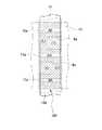
第1の実施形態では、R、G、Bの異なる色に対応する各サブ画素領域28R,28G,28Bを区画する遮光部14が設けられていた。これに対して、本実施形態では、遮光部14が設けられておらず、着色領域Cと非着色領域Hの双方が、各サブ画素領域28R,28G,28Bの長手方向に沿うコモン電極17の周縁部と平面的に重なるように設けられている。非着色領域Hは、各サブ画素領域28R,28G,28Bの図3における横方向(短手方向)に帯状に延在して設けられている。R、G、Bの異なる色に対応する各サブ画素領域28R,28G,28B間で着色領域C、非着色領域Hの面積がそれぞれ異なっている点は、第1の実施形態と同様である。
【0037】
本実施形態の液晶表示装置においても、反射モード、透過モード双方ともに発色が良く、視認性の高い表示が得られる、という第1の実施形態と同様の効果を得ることができる。また、着色領域Cと非着色領域Hの双方を各サブ画素領域28R,28G,28Bの長手方向に沿うコモン電極17の周縁部と平面的に重なるように設けているため、コモン電極17の周縁部でディスクリネーションが発生したとしても、ディスクリネーションによるコントラスト低下の影響を着色領域Cと非着色領域Hの双方で分け合うことになる。例えば、ディスクリネーションの発生がひどい場合は白色光、着色光の反射率がともに大きく低下し、ディスクリネーションがほとんど発生しない場合は白色光、着色光の反射率がともに維持される。すなわち、重畳される白色光と着色光の割合はいずれの場合もさほど変わらない。したがって、ディスクリネーションの発生の程度によって全体の反射率、すなわち反射表示の明るさは若干変わるものの、色純度のバラツキを従来に比べて低減することができる。
【0038】
なお、第1、第2の実施形態では、各サブ画素領域28R,28G,28Bの中央部に透過領域Tを1個所のみ設けた例を示したが、この構成に代えて、図4に示す構成としても良い。図4の構成は、各サブ画素領域28R,28G,28B内に透過領域Tを2個所設け、その2個所の透過領域Tを離間して配置するとともに、各サブ画素領域28R,28G,28Bの長手方向に延びる相対する辺(図4の縦方向に延びる右側の辺と左側の辺)にそれぞれ重なるように配置している。そして、図4では縦方向には1画素分しか示していないが、縦方向に並ぶ複数の画素29にわたって複数の透過領域Tが千鳥状に配置されている。
【0039】
例えば、第1、第2の実施形態のように各サブ画素領域28R,28G,28Bの中央に透過領域Tを1個所のみ設けた場合、特に透過領域Tが小さいと、透過表示Tに寄与する領域が各サブ画素領域28R,28G,28Bの中央に小さく点在する状態となるため、透過モードで見たときにざらつき感が感じられることがある。その点、上記の構成によれば、透過領域Tが千鳥状に散在する状態となるため、ざらつき感を低減することができる。
【0040】
さらに図4の例では、異なる色のサブ画素領域28R,28G,28B間でGのサブ画素領域28Gにおける透過領域Tの面積が最も小さく、次にRのサブ画素領域28Bにおける透過領域Tが小さく、Bのサブ画素領域28Rにおける透過領域Tが最も大きくなっている。言い換えると、Gのサブ画素領域28Gにおける反射領域Rの面積が最も大きく、次にRのサブ画素領域28Bにおける反射領域Rが大きく、Bのサブ画素領域28Rにおける反射領域Rが最も小さくなっている。また、非着色領域Hの面積が各サブ画素領域28R,28G,28Bで異なるのは第1、第2の実施形態と同様である。
【0041】
この場合、R、G、Bの各色毎に反射率と反射モード時の各色光の彩度、透過率と透過モード時の各色光の彩度を調整することができるので、反射モード時の表示の明るさと色度(例えば白表示時の色相)、透過モード時の表示の明るさと色度(例えば白表示時の色相)を適宜調整することができる。これにより、反射モード時と透過モード時の表示品位をバランス良く最適化することができる。
【0042】
なお、透過領域Tを複数設ける場合、2つに限ることはなく、任意の数としてもよい。しかしながら、透過領域Tの数を多くする程、同じ面積を確保するにあたって透過領域Tの周長が長くなる。その場合、製造プロセスにおけるエッチング等の加工バラツキによる透過領域Tの面積バラツキが大きくなり、その結果、透過モード、反射モード双方の表示の明るさバラツキが大きくなることが考えられる。したがって、表示のざらつき感と明るさバラツキとのバランスを考慮して透過領域Tの数を決める必要がある。その点で、透過領域Tを複数設ける場合には2個程度とするのが望ましい。
【0043】
図5は、1画素を構成するサブ画素領域のうち、例えばRのサブ画素領域28Rのみを図示したものである。第1、第2の実施形態では上下2個所に帯状の非着色領域Hを設けたが、図5に示すように、例えば上下2個所と中央1個所の計3個所に帯状の非着色領域Hを設けてもよい。サブ画素領域全体で同じ非着色領域Hの面積を確保する場合、当然ながら、数を多くした方が1個所あたりの非着色領域Hの面積、ひいては非着色領域Hの幅が狭くて済む。非着色領域Hの幅が狭ければオーバーコート膜16による平坦化が容易となり、カラーフィルター15の段差に起因する表示上の不具合が起こりにくくなる。
【0044】
また、上記実施形態では幅が一定の帯状の非着色領域Hを設けたが、例えば図6に示すように、中央に幅広部を有する帯状の非着色領域Hを設け、それに伴って異なる形状の透過領域Tを設けても良い。あるいは、図7に示すように、中央に幅狭部を有する帯状の非着色領域Hを設け、それに伴って異なる形状の透過領域Tを設けても良い。さらには、図8に示すように、非着色領域Hをサブ画素領域28Rの短手方向に連続した帯状とせず、図8のサブ画素領域28Rの縦方向に延びる右側の辺と左側の辺でそれぞれ孤立した非着色領域Hを設けても良い。ただしこの場合には、同じ面積を確保するのに必要な非着色領域Hの幅は帯状の場合に比べて広くなるため、オーバーコート膜16による平坦化が容易になる効果は得難くなる。また、2個所の透過領域Tは、必ずしも千鳥状に配置しなくても良い。また、図9に示すように、非着色領域Hを千鳥状に配置しても良い。この構成によれば、非着色領域Hが横方向に連続的につながらないため、文字等を表示した場合にボケ感が少なくなる。
【0045】
[電子機器]
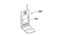
上記実施の形態の液晶表示装置を備えた電子機器の例について説明する。
図10は、携帯電話の一例を示した斜視図である。図10において、符号1000は携帯電話本体を示し、符号1001は上記の液晶表示装置を用いた液晶表示部を示している。
図10に示す電子機器は、上記実施の形態の液晶表示装置を用いた液晶表示部を備えているので、反射モード時にも透過モード時にも発色が良く、視認性に優れた液晶表示部を備えた電子機器を実現することができる。
【0046】
なお、本発明の技術範囲は上記実施の形態に限定されるものではなく、本発明の趣旨を逸脱しない範囲において種々の変更を加えることが可能である。例えば上記実施形態では、反射層として平坦な金属膜からなるものを用いたが、金属膜に微細なスリットを設けた反射偏光層からなるものを用いることもできる。その場合、下基板側から入射する透過表示に寄与する光の一部を反射して再利用することができ、透過表示の明るさを向上することができる。また、上記実施の形態ではカラーフィルターのパターンが縦ストライプである例を挙げたが、その他、横ストライプ、モザイク、デルタ配列等のカラーフィルターにも本発明が適用可能である。さらに、上記実施の形態で例示したパッシブマトリクス型液晶表示装置に限らず、TFD(薄膜ダイオード)、TFTをスイッチング素子としたアクティブマトリクス型液晶表示装置に本発明を適用することもできる。
【図面の簡単な説明】
【図1】 本発明の第1実施形態の液晶表示装置の画素を拡大視した平面図である。
【図2】 図1のA−A’線に沿う断面図である。
【図3】 第2実施形態の液晶表示装置の画素を拡大視した平面図である。
【図4】 同、液晶表示装置のパターンの変形例を示す平面図である。
【図5】 同、液晶表示装置のパターンの他の変形例を示す平面図である。
【図6】 同、液晶表示装置のパターンの他の変形例を示す平面図である。
【図7】 同、液晶表示装置のパターンの他の変形例を示す平面図である。
【図8】 同、液晶表示装置のパターンの他の変形例を示す平面図である。
【図9】 同、液晶表示装置のパターンの他の変形例を示す平面図である。
【図10】 本発明の電子機器の一例を示す斜視図である。
【図11】 従来の半透過反射型カラー液晶表示装置の平面図である。
【符号の説明】
1…液晶表示装置、3…バックライト(照明手段)、4…下基板、5…上基板、7…液晶層、8…反射層、8a…(反射層の)開口部、10…セグメント電極、13R,13G,13B…色素層、14…遮光部、15…カラーフィルター、17…コモン電極、28R,28G,28B…サブ画素領域、29…画素、C…着色領域、H…非着色領域、L…反射領域、T…透過領域[0001]
BACKGROUND OF THE INVENTION
The present invention relates to a liquid crystal display device and an electronic apparatus, and more particularly to a configuration of a transflective liquid crystal display device having an excellent balance of color purity in a reflection mode and a transmission mode.
[0002]
[Prior art]
There has been proposed a liquid crystal display device that uses external light such as sunlight and illumination light in a bright place, and can display using an internal light source such as a backlight in a dark place. In other words, this liquid crystal display device employs a display method that combines both a reflective type and a transmissive type, and the power consumption can be reduced by switching to either the reflective mode or the transmissive mode depending on the ambient brightness. Even when the surroundings are dark, the display can be clearly displayed. Hereinafter, in this specification, this type of liquid crystal display device is referred to as a “transflective liquid crystal display device”. In recent years, with the development of portable electronic devices and OA devices, colorization is often required also in the field of transflective liquid crystal display devices. As a transflective color liquid crystal display device that satisfies this requirement, one having a color filter on either an upper substrate or a lower substrate is provided. In the case of this type of liquid crystal display device, in the reflection mode, external light incident from the upper substrate side is transmitted through the color filter, then reflected by the reflection layer, and transmitted through the color filter again. In the transmission mode, the illumination light incident on the lower substrate from the backlight is transmitted through the color filter. In a normal configuration, display is performed using the same color filter in both the reflection mode and the transmission mode.
[0003]
In this liquid crystal display device, as described above, the color display can be obtained by transmitting the incident light through the color filter twice in the reflection mode and once in the transmission mode. For this reason, for example, when a light color filter is provided with an emphasis on the color in the reflection mode that transmits twice through the color filter, a display with good color can be obtained in the transmission mode that transmits only once through the color filter. Is difficult. However, on the contrary, when a dark color filter is provided with an emphasis on the color in the transmission mode that transmits once through the color filter, the display in the reflection mode that transmits twice through the color filter becomes dark. , Sufficient visibility will not be obtained. As described above, in the conventional transflective color liquid crystal display device, it is difficult to obtain a display with high visibility and high visibility both in the reflection mode and in the transmission mode.
[0004]
In order to solve the above problem, a liquid crystal display device having a configuration shown in FIG. 11 has been proposed (see, for example, Patent Document 1). This liquid crystal display device is an example of an active matrix liquid crystal display device, in which a
[0005]
In this configuration, a part of the light incident from the upper substrate side in the reflection mode is transmitted through the non-colored region H, and the light obtained by transmitting the color filter twice in the reflection mode is the non-colored region. The uncolored light (white light) that transmits H and the colored light that transmits the colored region C are superimposed. On the other hand, all the light transmitted through the transmission region T from the backlight in the transmission mode is transmitted through the colored region C, and the light obtained by transmitting once through the color filter in the transmission mode is all colored light. Become. In this way, the color density difference between the light obtained by transmitting twice through the color filter in the reflection mode and the light obtained by transmitting once through the color filter in the transmission mode can be reduced. By optimizing the dye layer of the filter, the color is good both in the reflection mode and in the transmission mode, and a display with high visibility can be obtained.
[0006]
[Patent Document 1]
JP 2000-111902 A
[0007]
[Problems to be solved by the invention]
However, in the conventional liquid crystal display device described in
[0008]
The present invention has been made in order to solve the above-described problems, and in a transflective color liquid crystal display device, a liquid crystal that exhibits good color development in both the reflection mode and the transmission mode and has little variation in color purity. An object is to provide a display device. Furthermore, an object of the present invention is to provide an electronic apparatus including the liquid crystal display device having excellent display quality.
[0009]
[Means for Solving the Problems]
In order to achieve the above object, the liquid crystal display device of the present invention comprises:A plurality of sub-pixel regions each consisting of a reflective region and a transmissive region and corresponding to different colors; A pair of substrates opposed to each other; a liquid crystal layer sandwiched between the pair of substrates;A pair of electrodes for driving the liquid crystal layer; A reflective layer provided in the reflective region;Overlapping the reflective layer A translucent reflection type display having a color filter in which a dye layer is arranged corresponding to each sub-pixel region, and performing display in each of the sub-pixels by the reflection region and a transmission region where the reflection layer is not present In the liquid crystal display device, a colored region where the dye layer is present and a non-colored region where the dye layer is not present are provided in the reflective region, and both the colored region and the non-colored region areIn one of the pair of electrodes Provided so as to overlap with the peripheral edge along the longitudinal direction of the sub-pixel region,The non-colored region extends across the pixel region in the short direction of the sub-pixel region, and the non-colored region in one sub-pixel among adjacent sub-pixels among the plurality of sub-pixel regions. Is formed in a region on an extension line in the short direction with respect to the non-colored region in the other sub-pixel, and the area of each non-colored region is different It is characterized by that. The “sub-pixel region” referred to here is a basic unit region that constitutes one full-color pixel in a display region corresponding to a plurality of different colors.
[0010]
As exemplified in the section of [Prior Art], a liquid crystal display device in which a non-colored region of a color filter is provided in a reflective region is excellent in that the color is good in both the reflection mode and the transmission mode. However, there was a problem that the variation in color purity was large. As a result of investigating the cause, the present inventors have found that the liquid crystal disclination (alignment disorder) occurring at the edge of the electrode in each sub-pixel region is one of the causes of variations in color purity. . In other words, the electric field (electric field lines) generated in the liquid crystal layer between the upper and lower substrates in the portion near the center of the electrode in each subpixel region acts in a direction perpendicular to the substrate surface, but the electric field (electric force) at the periphery of the electrode. Line) acts obliquely with respect to the substrate surface. Further, a lateral electric field between adjacent electrodes also acts at the peripheral edge of the electrode. As a result, the occurrence of liquid crystal disclination cannot be avoided at the peripheral edge of the electrode, and the contrast is lowered. The degree of occurrence of disclination varies depending on the electric field application state between the electrodes and manufacturing variations of individual liquid crystal display devices. Further, when the sub-pixel region has an elongated shape (for example, a rectangular shape), the peripheral portion of the electrode along the longitudinal direction has a larger area of the disclination generation region than the short-side direction. A large impact.
[0011]
Here, looking again at the configuration of the conventional liquid crystal display device shown in FIG. 11, the
[0012]
On the other hand, the liquid crystal display device of the present invention is characterized in that both the colored region and the non-colored region are provided so as to overlap with the peripheral portion of the electrode along the longitudinal direction of the sub-pixel region. That is, the peripheral portions of the electrodes along the longitudinal direction of the sub-pixel region are not overlapped with only one of the colored region and the non-colored region, but are arranged so as to be shared in both the colored region and the non-colored region. As a result, even if disclination occurs at the peripheral edge of the electrode, the influence of contrast reduction due to disclination is shared between the colored region and the non-colored region. For example, when the occurrence of disclination is severe, the reflectance of white light and colored light is greatly reduced, and when the disclination hardly occurs, both the reflectance of white light and colored light are maintained. That is, regardless of the degree of occurrence of disclination, the ratio of the superimposed white light and colored light is not changed as in the conventional case. Therefore, although the overall reflectance, that is, the brightness of the reflective display changes slightly depending on the degree of occurrence of disclination, the variation in color purity can be reduced as compared with the conventional case.
[0013]
Alternatively, in order to achieve the above object, another liquid crystal display device according to the present invention includes a pair of substrates each composed of an upper substrate and a lower substrate disposed to face each other, and a liquid crystal layer sandwiched between the pair of substrates. An electrode for driving the liquid crystal layer provided on each of the pair of substrates, a reflective layer partially provided on the inner surface side of the lower substrate and reflecting incident light from the upper substrate side, and the reflective layer A color filter in which a dye layer of a different color is arranged corresponding to each sub-pixel region constituting the display region, a light-shielding layer that partitions the adjacent sub-pixel regions, and the lower A transflective liquid crystal display having an illumination means provided on the outer surface side of the substrate and performing display in a reflective area where the reflective layer exists and a transmissive area where the reflective layer does not exist for each sub-pixel area A device in the reflective area; A colored region in which the pigment layer of the color filter is present and a non-colored region in which the pigment layer is not present are provided, and both the colored region and the non-colored region are along the longitudinal direction of the sub-pixel region. It is characterized by being provided so as to overlap with the plane.
[0014]
In the above description, attention was paid to the liquid crystal disclination generated at the peripheral edge of the electrode as one of the causes of the color purity variation. Furthermore, the present inventors have further paid attention to the dimensional variation of the light-shielding layer in the manufacturing process in the liquid crystal display device including the light-shielding layer (so-called black matrix) that partitions the adjacent sub-pixel regions as another cause. . That is, between the adjacent sub-pixel regions, a lattice-shaped light-shielding layer may be provided in order to hide light leakage due to disclination at the peripheral edge of the electrode or to prevent color mixing of each color light transmitted through the color filter. is there. However, the dimensional variation of the light shielding layer in the manufacturing process is unavoidable, and accordingly, the reflectance at the peripheral portion of the sub-pixel region varies. Further, when the sub-pixel region has a long and narrow shape (for example, a rectangular shape), the peripheral portion of the sub-pixel region along the longitudinal direction has a larger influence of variation due to the longer peripheral length than the short-side direction.
[0015]
In this case as well, as in the case of the conventional liquid crystal display device, if the peripheral portions of the electrodes along the longitudinal direction of the sub-pixel region are all non-colored regions, the reflectance of the colored light is substantially constant. When the width of the light shielding layer is larger than the design value, the reflectance of white light is greatly reduced. When the width of the light shielding layer is as designed, the reflectance of white light is maintained. This proved to be a factor in the variation in color purity. On the contrary, the same applies to the case where all the peripheral portions of the electrodes along the longitudinal direction are colored regions.
[0016]
On the other hand, the liquid crystal display device of the present invention is characterized in that both the colored region and the non-colored region are provided so as to overlap with the light shielding layer extending along the longitudinal direction of the sub-pixel region. . That is, the light-shielding layer along the longitudinal direction of the sub-pixel region is arranged not to overlap only one of the colored region and the non-colored region but to be shared by both the colored region and the non-colored region. As a result, even if the dimensional variation of the light shielding layer occurs, the variation in reflectance is shared between the colored region and the non-colored region. For example, when the width of the light shielding layer is increased, the reflectances of white light and colored light are both lowered, and when the width of the light shielding layer is normal, both the reflectances of white light and colored light are maintained. That is, in any case, the ratio of the white light and the colored light to be superimposed is not different from that of the conventional one. Therefore, although the overall reflectance, that is, the brightness of the reflective display slightly changes depending on the dimensional variation of the light shielding layer, the variation in color purity can be reduced as compared with the conventional case.
[0017]
The shape of the non-colored region is not limited as long as both the colored region and the non-colored region overlap with the peripheral portion of the electrode along the longitudinal direction of the sub-pixel region or the light shielding layer along the longitudinal direction of the sub-pixel region. It may be. However, it is desirable that the non-colored region extends in a strip shape in the short direction of the sub-pixel region.
According to this configuration, even when the area of the same non-colored region is ensured, the width in the short direction of the non-colored region can be further reduced. In general, since the colored layer of the color filter is thicker than the other layers constituting the liquid crystal display device, the step between the colored region and the non-colored region is relatively large. In this case, if the width of the non-colored region in the short direction is wide, it becomes difficult to planarize with an overcoat film for relaxing the step of the color filter. On the other hand, if the width of the non-colored region of the color filter is narrow, the flattening is easy, and display defects due to the steps of the color filter are less likely to occur.
[0018]
Further, regarding the form of the transmissive region, it may be arbitrarily designed and arranged while ensuring a necessary area. For example, a plurality of transmissive regions are provided in the sub-pixel region, and the plurality of transmissive regions are arranged separately from each other. It is good also as a structure.
In particular, when the transmissive region is relatively small, the region contributing to the transmissive display is scattered in a part of the sub-pixel region, so that a rough feeling may be felt by human eyes. In that respect, according to the above configuration, the region contributing to the transmissive display is scattered in the sub-pixel region, so that the feeling of roughness is reduced.
When a plurality of transmissive regions are arranged in a staggered manner over a plurality of sub-pixel regions, the above-described roughness is further reduced.
[0019]
Further, among the sub-pixel regions corresponding to different colors, the area of the non-colored region in the sub-pixel region corresponding to at least one color is made different from the area of the non-colored region in the sub-pixel region corresponding to the other color. May be.
According to this configuration, since the reflectance and the color purity of each color light can be adjusted for each sub-pixel region corresponding to a different color, the reflectance and chromaticity as a whole reflected light (for example, hue at the time of white display) Can be adjusted as appropriate, and display quality such as display brightness and color in the reflection mode can be improved.
[0020]
More specifically, when the different color pigment layers are composed of a red layer, a green layer, and a blue layer, the area of the non-colored region in the sub-pixel region corresponding to the green layer corresponds to the red layer and the blue layer. It is desirable to make it larger than the area of the non-colored region in the sub-pixel region.
Green light has a much higher visibility for the human eye than red light and blue light. Therefore, by setting the area of the non-colored region in the green sub-pixel region to be larger than the area of the non-colored region in the red or blue sub-pixel region, the reflectance and color reproducibility when viewed as a whole reflected light can be obtained. Can be improved.
[0021]
Further, the above-described configuration is adopted, and among the sub-pixel areas corresponding to different colors, the area of the transmission area in the sub-pixel area corresponding to at least one color is the transmission area in the sub-pixel area corresponding to the other color. It may be different from the area.
According to this configuration, since the transmittance and the color purity of each color light can be adjusted for each sub-pixel region corresponding to a different color, the transmittance and chromaticity as a whole of the transmitted light (for example, the hue during white display) Can be adjusted as appropriate. Therefore, the optical characteristics such as reflectance, transmittance, chromaticity of reflected light, chromaticity of transmitted light, etc. can be adjusted by performing in combination with the adjustment of the area of the non-colored region. And display quality in the transmission mode can be optimized with a good balance.
[0022]
More specifically, when the pigment layers of different colors are composed of a red layer, a green layer, and a blue layer, the area of the transmissive region in the sub pixel region corresponding to the green layer is set to the sub layer corresponding to the red layer and the blue layer. It is desirable to make it smaller than the area of the transmissive region in the pixel region.
As described above, since green light has higher visibility than red light and blue light, the area of the transmission region in the green sub-pixel region is larger than the area of the transmission region in the red and blue sub-pixel regions. Even if it is set to a small value, the color balance does not deteriorate, and a sufficient transmittance can be maintained.
[0023]
The reflective layer may be made of a metal film, or may be made of a reflective polarizing layer in which fine slits are provided in the metal film. In particular, if it is made of the reflective polarizing layer, part of the light contributing to the transmissive display incident from the lower substrate side can be reflected and reused, and the brightness of the transmissive display can be improved.
[0024]
An electronic apparatus according to the present invention includes the liquid crystal display device according to the present invention. According to this configuration, it is possible to provide an electronic device including a liquid crystal display unit that has good color development and excellent visibility in both the reflection mode and the transmission mode.
[0025]
DETAILED DESCRIPTION OF THE INVENTION
[First Embodiment]
Hereinafter, a first embodiment of the present invention will be described with reference to FIGS.
The liquid crystal display device of this embodiment is an example of a passive matrix transflective color liquid crystal display device.
1 is an enlarged plan view of one pixel constituting a display area of the liquid crystal display device of the present embodiment, and FIG. 2 is a cross-sectional view taken along the line AA ′ of FIG. In the following drawings, the film thicknesses and dimensional ratios of the respective components are appropriately changed in order to make the drawings easy to see.
[0026]
As shown in FIG. 2, the liquid
[0027]
On the inner surface side of the
[0028]
A retardation plate (¼ wavelength plate) 20 and a
[0029]
The arrangement of the patterns on each of the
[0030]
In the present embodiment, the
[0031]
Further, the R, G, and B dye layers 13R, 13G, and 13B of the
[0032]
In this embodiment, when viewed between the
[0033]
In the liquid
[0034]
Further, in the liquid
[0035]
[Second Embodiment]
Hereinafter, a second embodiment of the present invention will be described with reference to FIG.
FIG. 3 is a plan view in which the pixels constituting the display area of the liquid crystal display device of this embodiment are enlarged, and corresponds to FIG. 1 of the first embodiment. The basic configuration of the liquid crystal display device of the present embodiment is the same as that of the first embodiment, and is different from the first embodiment only in that there is no light shielding portion. 3, the same components as those in FIG. 2 are denoted by the same reference numerals, and detailed description thereof is omitted.
[0036]
In the first embodiment, the light-shielding
[0037]
Also in the liquid crystal display device of this embodiment, the same effects as those of the first embodiment can be obtained that both the reflection mode and the transmission mode are well-colored and display with high visibility can be obtained. Further, since both the colored region C and the non-colored region H are provided so as to overlap the peripheral portion of the
[0038]
In the first and second embodiments, an example in which only one transmission region T is provided at the center of each of the
[0039]
For example, when only one transmissive region T is provided at the center of each of the
[0040]
Further, in the example of FIG. 4, the area of the transmission region T in the
[0041]
In this case, the reflectance and the saturation of each color light in the reflection mode and the transmittance and the saturation of each color light in the transmission mode can be adjusted for each color of R, G, and B. Brightness and chromaticity (for example, hue at the time of white display), and display brightness and chromaticity at the time of the transmission mode (for example, hue at the time of white display) can be adjusted as appropriate. Thereby, the display quality in the reflection mode and the transmission mode can be optimized with a good balance.
[0042]
Note that when a plurality of transmission regions T are provided, the number is not limited to two and may be any number. However, the larger the number of transmission regions T, the longer the circumference of the transmission region T in securing the same area. In that case, the variation in the area of the transmission region T due to processing variations such as etching in the manufacturing process increases, and as a result, the display brightness in both the transmission mode and the reflection mode may increase. Therefore, it is necessary to determine the number of transmissive regions T in consideration of the balance between display roughness and brightness variation. In this respect, when a plurality of transmission regions T are provided, it is desirable that the number is about two.
[0043]
FIG. 5 illustrates, for example, only the
[0044]
Moreover, in the said embodiment, although the strip-shaped non-colored area | region H with constant width was provided, as shown, for example in FIG. 6, the strip-shaped non-colored area | region H which has a wide part in the center is provided, and the shape of a different shape in connection with it. A transmissive region T may be provided. Alternatively, as shown in FIG. 7, a strip-shaped non-colored region H having a narrow portion at the center may be provided, and a transmission region T having a different shape may be provided accordingly. Furthermore, as shown in FIG. 8, the non-colored region H is not formed as a continuous belt in the short direction of the
[0045]
[Electronics]
Examples of electronic devices provided with the liquid crystal display device of the above embodiment will be described.
FIG. 10 is a perspective view showing an example of a mobile phone. In FIG. 10,
Since the electronic device shown in FIG. 10 includes a liquid crystal display unit using the liquid crystal display device of the above embodiment, the electronic device includes a liquid crystal display unit that has good color development in both the reflection mode and the transmission mode and has excellent visibility. Electronic devices can be realized.
[0046]
The technical scope of the present invention is not limited to the above embodiment, and various modifications can be made without departing from the spirit of the present invention. For example, in the above embodiment, the reflective layer made of a flat metal film is used, but a reflective film made of a reflective polarizing layer in which fine slits are provided in the metal film can also be used. In that case, part of the light contributing to the transmissive display incident from the lower substrate side can be reflected and reused, and the brightness of the transmissive display can be improved. In the above embodiment, the color filter pattern is a vertical stripe. However, the present invention can also be applied to color filters such as horizontal stripes, mosaics, and delta arrangements. Furthermore, the present invention can be applied not only to the passive matrix liquid crystal display device exemplified in the above embodiment, but also to an active matrix liquid crystal display device using TFD (thin film diode) and TFT as switching elements.
[Brief description of the drawings]
FIG. 1 is an enlarged plan view of a pixel of a liquid crystal display device according to a first embodiment of the present invention.
FIG. 2 is a cross-sectional view taken along the line AA ′ of FIG.
FIG. 3 is an enlarged plan view of a pixel of a liquid crystal display device according to a second embodiment.
FIG. 4 is a plan view showing a modification of the pattern of the liquid crystal display device.
FIG. 5 is a plan view showing another modification of the pattern of the liquid crystal display device.
FIG. 6 is a plan view showing another modification of the pattern of the liquid crystal display device.
FIG. 7 is a plan view showing another modification of the pattern of the liquid crystal display device.
FIG. 8 is a plan view showing another modification of the pattern of the liquid crystal display device.
FIG. 9 is a plan view showing another modification of the pattern of the liquid crystal display device.
FIG. 10 is a perspective view illustrating an example of an electronic apparatus according to the invention.
FIG. 11 is a plan view of a conventional transflective color liquid crystal display device.
[Explanation of symbols]
DESCRIPTION OF
Claims (5)
Translated fromJapanese前記反射領域内に、前記色素層が存在する着色領域と前記色素層が存在しない非着色領域とが設けられ、
前記着色領域と前記非着色領域の双方が、前記一対の電極のうち一方の電極における前記サブ画素領域の長手方向に沿う周縁部と重なるように設けられ、
前記非着色領域は、前記サブ画素領域の短手方向に当該画素領域を横断するように延在し、
前記複数のサブ画素領域のうち隣接するサブ画素同士において、一方のサブ画素における非着色領域が他方のサブ画素における非着色領域に対して短手方向の延長線上の領域に形成されるとともに、各々の非着色領域の面積が異なる
ことを特徴とする液晶表示装置。A plurality of sub-pixel regions each composed of areflective region and a transmissive region and corresponding to different colors, a pair of substrates arranged opposite to each other, a liquid crystal layer sandwiched between the pair of substrates, and a pairfor driving the liquid crystal layer And a color filter in which a dye layer is arranged corresponding to each of the sub-pixel regions so asto overlap with the reflective layer, and thereflection for each sub-pixel. A transflective liquid crystal display device that performs display in a region and a transmissive region in which the reflective layer does not exist,
In the reflective region, a colored region where the dye layer is present and a non-colored region where the dye layer is not present are provided,
Both the colored region and the non-colored region are provided so as to overlap with a peripheral edge along the longitudinal direction of the sub-pixel regionin one of the pair of electrodes ,
The non-colored region extends so as to cross the pixel region in the short direction of the sub-pixel region,
In adjacent subpixels of the plurality of subpixel regions, a non-colored region in one subpixel is formed in a region on an extension line in a short direction with respect to the noncolored region in the other subpixel, and each A liquid crystal display device characterized in that theareas of the non-colored regions are different .
Priority Applications (6)
| Application Number | Priority Date | Filing Date | Title |
|---|---|---|---|
| JP2003116365AJP3918765B2 (en) | 2003-04-21 | 2003-04-21 | Liquid crystal display device and electronic device |
| US10/808,405US7176997B2 (en) | 2003-04-21 | 2004-03-25 | Liquid crystal display device and electronic apparatus |
| TW093111022ATWI257501B (en) | 2003-04-21 | 2004-04-20 | Liquid crystal display device and electronic apparatus |
| KR1020040026993AKR100648754B1 (en) | 2003-04-21 | 2004-04-20 | Liquid crystal display device and electronic apparatus |
| CNB2004100327791ACN100397152C (en) | 2003-04-21 | 2004-04-21 | Liquid crystal display device and electronic equipment |
| US11/503,949US7321410B2 (en) | 2003-04-21 | 2006-08-15 | Liquid crystal display device and electronic apparatus |
Applications Claiming Priority (1)
| Application Number | Priority Date | Filing Date | Title |
|---|---|---|---|
| JP2003116365AJP3918765B2 (en) | 2003-04-21 | 2003-04-21 | Liquid crystal display device and electronic device |
Publications (2)
| Publication Number | Publication Date |
|---|---|
| JP2004325528A JP2004325528A (en) | 2004-11-18 |
| JP3918765B2true JP3918765B2 (en) | 2007-05-23 |
Family
ID=33487045
Family Applications (1)
| Application Number | Title | Priority Date | Filing Date |
|---|---|---|---|
| JP2003116365AExpired - LifetimeJP3918765B2 (en) | 2003-04-21 | 2003-04-21 | Liquid crystal display device and electronic device |
Country Status (5)
| Country | Link |
|---|---|
| US (2) | US7176997B2 (en) |
| JP (1) | JP3918765B2 (en) |
| KR (1) | KR100648754B1 (en) |
| CN (1) | CN100397152C (en) |
| TW (1) | TWI257501B (en) |
Families Citing this family (46)
| Publication number | Priority date | Publication date | Assignee | Title |
|---|---|---|---|---|
| TWI289708B (en) | 2002-12-25 | 2007-11-11 | Qualcomm Mems Technologies Inc | Optical interference type color display |
| TWI247921B (en)* | 2003-09-10 | 2006-01-21 | Seiko Epson Corp | Electrooptic device, color filter substrate, manufacturing method for electrooptic device and electronic equipment |
| JP4484504B2 (en)* | 2003-12-12 | 2010-06-16 | オプトレックス株式会社 | Transflective color liquid crystal display element |
| US7342705B2 (en) | 2004-02-03 | 2008-03-11 | Idc, Llc | Spatial light modulator with integrated optical compensation structure |
| US7855824B2 (en) | 2004-03-06 | 2010-12-21 | Qualcomm Mems Technologies, Inc. | Method and system for color optimization in a display |
| US7911428B2 (en) | 2004-09-27 | 2011-03-22 | Qualcomm Mems Technologies, Inc. | Method and device for manipulating color in a display |
| US7807488B2 (en) | 2004-09-27 | 2010-10-05 | Qualcomm Mems Technologies, Inc. | Display element having filter material diffused in a substrate of the display element |
| US7710632B2 (en) | 2004-09-27 | 2010-05-04 | Qualcomm Mems Technologies, Inc. | Display device having an array of spatial light modulators with integrated color filters |
| US7928928B2 (en) | 2004-09-27 | 2011-04-19 | Qualcomm Mems Technologies, Inc. | Apparatus and method for reducing perceived color shift |
| US8362987B2 (en) | 2004-09-27 | 2013-01-29 | Qualcomm Mems Technologies, Inc. | Method and device for manipulating color in a display |
| US7898521B2 (en) | 2004-09-27 | 2011-03-01 | Qualcomm Mems Technologies, Inc. | Device and method for wavelength filtering |
| JP2006201433A (en)* | 2005-01-20 | 2006-08-03 | Toppan Printing Co Ltd | Method of manufacturing color filter for transflective liquid crystal display device and color filter for transflective liquid crystal display device |
| JP4127272B2 (en)* | 2005-03-02 | 2008-07-30 | セイコーエプソン株式会社 | Electro-optical device substrate, electro-optical device, and electronic apparatus |
| JP2006251417A (en)* | 2005-03-11 | 2006-09-21 | Hitachi Displays Ltd | Liquid crystal display |
| US7423713B2 (en)* | 2005-03-28 | 2008-09-09 | Epson Imaging Devices Corporation | Liquid crystal device and electronic equipment |
| JP2006284611A (en)* | 2005-03-31 | 2006-10-19 | Alps Electric Co Ltd | Semitransmissive liquid crystal display panel and color liquid crystal display device |
| CN100410764C (en)* | 2005-05-19 | 2008-08-13 | 爱普生映像元器件有限公司 | Electro-optical devices and electronic equipment |
| JP4197000B2 (en)* | 2005-07-07 | 2008-12-17 | エプソンイメージングデバイス株式会社 | Electro-optical device and electronic apparatus |
| KR101182771B1 (en)* | 2005-09-23 | 2012-09-14 | 삼성전자주식회사 | Liquid crystal display panel and method of driving the same and liquid crystal display apparatus using the same |
| KR101219042B1 (en) | 2005-12-06 | 2013-01-07 | 삼성디스플레이 주식회사 | Transflective liquid crystal |
| CN100371794C (en)* | 2005-12-22 | 2008-02-27 | 友达光电股份有限公司 | color filter |
| KR20070084851A (en) | 2006-02-22 | 2007-08-27 | 삼성전자주식회사 | Semi-transmissive liquid crystal display device and display panel for same |
| US7990499B2 (en)* | 2006-03-20 | 2011-08-02 | Sharp Kabushiki Kaisha | Display device |
| JP5172656B2 (en)* | 2006-03-20 | 2013-03-27 | シャープ株式会社 | Display device |
| US8004743B2 (en) | 2006-04-21 | 2011-08-23 | Qualcomm Mems Technologies, Inc. | Method and apparatus for providing brightness control in an interferometric modulator (IMOD) display |
| KR101304410B1 (en) | 2006-09-19 | 2013-09-05 | 삼성디스플레이 주식회사 | Liquid crystal display device |
| EP1943555B1 (en) | 2006-10-06 | 2012-05-02 | QUALCOMM MEMS Technologies, Inc. | Optical loss structure integrated in an illumination apparatus of a display |
| EP1943551A2 (en) | 2006-10-06 | 2008-07-16 | Qualcomm Mems Technologies, Inc. | Light guide |
| TW200819886A (en) | 2006-10-16 | 2008-05-01 | Innolux Display Corp | Liquid crystal display device |
| TWI341399B (en)* | 2006-12-15 | 2011-05-01 | Chimei Innolux Corp | Liquid crystal panel and liquid crystal display device |
| KR20080070419A (en) | 2007-01-26 | 2008-07-30 | 삼성전자주식회사 | Semi-transmissive liquid crystal display and manufacturing method thereof |
| US8068710B2 (en) | 2007-12-07 | 2011-11-29 | Qualcomm Mems Technologies, Inc. | Decoupled holographic film and diffuser |
| JP2011507306A (en) | 2007-12-17 | 2011-03-03 | クォルコム・メムズ・テクノロジーズ・インコーポレーテッド | Photovoltaic device with interference backside mask |
| JP2011512006A (en) | 2008-01-30 | 2011-04-14 | デジタル オプティクス インターナショナル,リミティド ライアビリティ カンパニー | Thin lighting system |
| US8721149B2 (en) | 2008-01-30 | 2014-05-13 | Qualcomm Mems Technologies, Inc. | Illumination device having a tapered light guide |
| KR101290195B1 (en)* | 2008-07-28 | 2013-07-30 | 픽셀 키 코포레이션 | Transflective display with white tuning |
| JP5492899B2 (en) | 2008-10-10 | 2014-05-14 | クォルコム・メムズ・テクノロジーズ・インコーポレーテッド | Distributed lighting system |
| KR20110104090A (en) | 2009-01-13 | 2011-09-21 | 퀄컴 엠이엠스 테크놀로지스, 인크. | Large Area Light Panels and Screens |
| CN102449512A (en) | 2009-05-29 | 2012-05-09 | 高通Mems科技公司 | Illumination devices and methods of fabrication thereof |
| US8848294B2 (en) | 2010-05-20 | 2014-09-30 | Qualcomm Mems Technologies, Inc. | Method and structure capable of changing color saturation |
| US8402647B2 (en) | 2010-08-25 | 2013-03-26 | Qualcomm Mems Technologies Inc. | Methods of manufacturing illumination systems |
| US8416373B2 (en)* | 2011-04-06 | 2013-04-09 | Himax Display, Inc. | Display device and method for manufacturing the same |
| KR101316799B1 (en) | 2011-07-28 | 2013-10-11 | 하이맥스 디스플레이, 인크. | display device and method for manufacturing the same |
| DE202011106074U1 (en) | 2011-09-26 | 2011-11-02 | Gimbal Technology Co., Ltd. | Position detection device |
| CN104297996B (en)* | 2014-11-10 | 2018-03-27 | 上海天马微电子有限公司 | Color film substrate, liquid crystal display panel and display device |
| KR102513840B1 (en)* | 2017-11-15 | 2023-03-23 | 엘지디스플레이 주식회사 | Display panel |
Family Cites Families (17)
| Publication number | Priority date | Publication date | Assignee | Title |
|---|---|---|---|---|
| US6630970B2 (en)* | 2001-07-02 | 2003-10-07 | 3M Innovative Properties Company | Polarizers for use with liquid crystal displays |
| US6141070A (en)* | 1997-06-13 | 2000-10-31 | Citizen Watch Co., Ltd. | Normally black liquid crystal display with twisted compensator and . .DELTAnd of 1500-1800 nm |
| JP3738549B2 (en) | 1997-12-22 | 2006-01-25 | カシオ計算機株式会社 | Liquid crystal display element |
| JP3335130B2 (en) | 1998-01-26 | 2002-10-15 | シャープ株式会社 | Liquid crystal display |
| JP3410664B2 (en) | 1998-07-14 | 2003-05-26 | シャープ株式会社 | Liquid crystal display |
| JP3768367B2 (en)* | 1998-10-14 | 2006-04-19 | シャープ株式会社 | Liquid crystal display |
| DE60005760D1 (en)* | 1999-02-15 | 2003-11-13 | Citizen Watch Co Ltd | LIQUID CRYSTAL DISPLAY |
| US6456346B1 (en)* | 1999-10-13 | 2002-09-24 | Citizen Watch Co., Ltd. | Color liquid crystal display device including super twisted nematic liquid crystal with molecular major axis directions parallel to a display screen horizontal axis |
| JP2001174797A (en) | 1999-12-21 | 2001-06-29 | Kyocera Corp | Transflective liquid crystal display |
| JP4058875B2 (en)* | 2000-02-14 | 2008-03-12 | セイコーエプソン株式会社 | Color filter substrate, color filter substrate manufacturing method, liquid crystal device, liquid crystal device manufacturing method, and electronic apparatus |
| JP3941481B2 (en) | 2000-12-22 | 2007-07-04 | セイコーエプソン株式会社 | Liquid crystal display device and electronic device |
| TW581918B (en)* | 2001-03-07 | 2004-04-01 | Sharp Kk | Transmission/reflection type color liquid crystal display device |
| JP4398602B2 (en) | 2001-05-18 | 2010-01-13 | 株式会社日立製作所 | Liquid crystal display |
| JP4165132B2 (en) | 2001-07-27 | 2008-10-15 | セイコーエプソン株式会社 | Electro-optical device, color filter substrate, and electronic device |
| JP4264217B2 (en)* | 2001-09-25 | 2009-05-13 | シャープ株式会社 | Substrate with colored layer |
| JP2003177392A (en) | 2001-12-11 | 2003-06-27 | Kyocera Corp | Liquid crystal display |
| TWI326377B (en)* | 2003-05-09 | 2010-06-21 | Chimei Innolux Corp | Transflective color filter, transflective liquid display using the same and method of manufacturing the same |
- 2003
- 2003-04-21JPJP2003116365Apatent/JP3918765B2/ennot_activeExpired - Lifetime
- 2004
- 2004-03-25USUS10/808,405patent/US7176997B2/ennot_activeExpired - Lifetime
- 2004-04-20KRKR1020040026993Apatent/KR100648754B1/ennot_activeExpired - Lifetime
- 2004-04-20TWTW093111022Apatent/TWI257501B/ennot_activeIP Right Cessation
- 2004-04-21CNCNB2004100327791Apatent/CN100397152C/ennot_activeExpired - Lifetime
- 2006
- 2006-08-15USUS11/503,949patent/US7321410B2/ennot_activeExpired - Lifetime
Also Published As
| Publication number | Publication date |
|---|---|
| KR20040091561A (en) | 2004-10-28 |
| US20060274243A1 (en) | 2006-12-07 |
| CN1540393A (en) | 2004-10-27 |
| US20040246414A1 (en) | 2004-12-09 |
| JP2004325528A (en) | 2004-11-18 |
| CN100397152C (en) | 2008-06-25 |
| TWI257501B (en) | 2006-07-01 |
| US7176997B2 (en) | 2007-02-13 |
| KR100648754B1 (en) | 2006-11-23 |
| TW200424658A (en) | 2004-11-16 |
| US7321410B2 (en) | 2008-01-22 |
Similar Documents
| Publication | Publication Date | Title |
|---|---|---|
| JP3918765B2 (en) | Liquid crystal display device and electronic device | |
| JP3941481B2 (en) | Liquid crystal display device and electronic device | |
| KR100520613B1 (en) | A liquid crystal display device, a substrate for liquid crystal display device and electronic device | |
| US6501521B2 (en) | Transmission/reflection type color liquid crystal display device | |
| KR100259977B1 (en) | Color liquid crystal display element | |
| JP3738549B2 (en) | Liquid crystal display element | |
| JP3692445B2 (en) | Liquid crystal device and electronic device | |
| JP2007114303A (en) | Liquid crystal device and electronic apparatus | |
| JP3693055B2 (en) | Liquid crystal display device and electronic device | |
| JP3674582B2 (en) | Liquid crystal display device and electronic device | |
| JP4259502B2 (en) | Liquid crystal display device and electronic device | |
| JP4244977B2 (en) | Liquid crystal display device and electronic device | |
| JP4142075B2 (en) | Liquid crystal display device and electronic device | |
| JP4142074B2 (en) | Liquid crystal display device and electronic device | |
| JP2007047835A (en) | Liquid crystal display device and electronic device | |
| KR20040066139A (en) | Colour liquid crystal display device | |
| JP2003202557A (en) | Liquid crystal display and electronic equipment | |
| JP2003207769A (en) | Liquid crystal display and electronic equipment | |
| JP2004086222A (en) | Liquid crystal display and electronic equipment | |
| JP2007047840A (en) | Liquid crystal display device and electronic device | |
| JP2007114801A (en) | Liquid crystal display device and electronic device | |
| JP2007065693A (en) | Liquid crystal display device and electronic device | |
| JP2007047837A (en) | Liquid crystal display device and electronic device | |
| JP2007047836A (en) | Liquid crystal display device and electronic device | |
| JP2007047830A (en) | Liquid crystal display device and electronic device |
Legal Events
| Date | Code | Title | Description |
|---|---|---|---|
| A977 | Report on retrieval | Free format text:JAPANESE INTERMEDIATE CODE: A971007 Effective date:20051215 | |
| A131 | Notification of reasons for refusal | Free format text:JAPANESE INTERMEDIATE CODE: A131 Effective date:20060523 | |
| A521 | Request for written amendment filed | Free format text:JAPANESE INTERMEDIATE CODE: A523 Effective date:20060713 | |
| TRDD | Decision of grant or rejection written | ||
| A01 | Written decision to grant a patent or to grant a registration (utility model) | Free format text:JAPANESE INTERMEDIATE CODE: A01 Effective date:20070123 | |
| A61 | First payment of annual fees (during grant procedure) | Free format text:JAPANESE INTERMEDIATE CODE: A61 Effective date:20070205 | |
| R150 | Certificate of patent or registration of utility model | Ref document number:3918765 Country of ref document:JP Free format text:JAPANESE INTERMEDIATE CODE: R150 Free format text:JAPANESE INTERMEDIATE CODE: R150 | |
| FPAY | Renewal fee payment (event date is renewal date of database) | Free format text:PAYMENT UNTIL: 20110223 Year of fee payment:4 | |
| FPAY | Renewal fee payment (event date is renewal date of database) | Free format text:PAYMENT UNTIL: 20110223 Year of fee payment:4 | |
| FPAY | Renewal fee payment (event date is renewal date of database) | Free format text:PAYMENT UNTIL: 20120223 Year of fee payment:5 | |
| FPAY | Renewal fee payment (event date is renewal date of database) | Free format text:PAYMENT UNTIL: 20130223 Year of fee payment:6 | |
| FPAY | Renewal fee payment (event date is renewal date of database) | Free format text:PAYMENT UNTIL: 20130223 Year of fee payment:6 | |
| R250 | Receipt of annual fees | Free format text:JAPANESE INTERMEDIATE CODE: R250 | |
| S111 | Request for change of ownership or part of ownership | Free format text:JAPANESE INTERMEDIATE CODE: R313113 | |
| S111 | Request for change of ownership or part of ownership | Free format text:JAPANESE INTERMEDIATE CODE: R313113 | |
| R371 | Transfer withdrawn | Free format text:JAPANESE INTERMEDIATE CODE: R371 | |
| S111 | Request for change of ownership or part of ownership | Free format text:JAPANESE INTERMEDIATE CODE: R313113 | |
| R350 | Written notification of registration of transfer | Free format text:JAPANESE INTERMEDIATE CODE: R350 | |
| R250 | Receipt of annual fees | Free format text:JAPANESE INTERMEDIATE CODE: R250 | |
| R250 | Receipt of annual fees | Free format text:JAPANESE INTERMEDIATE CODE: R250 | |
| R250 | Receipt of annual fees | Free format text:JAPANESE INTERMEDIATE CODE: R250 | |
| R250 | Receipt of annual fees | Free format text:JAPANESE INTERMEDIATE CODE: R250 | |
| R250 | Receipt of annual fees | Free format text:JAPANESE INTERMEDIATE CODE: R250 | |
| R250 | Receipt of annual fees | Free format text:JAPANESE INTERMEDIATE CODE: R250 | |
| R250 | Receipt of annual fees | Free format text:JAPANESE INTERMEDIATE CODE: R250 | |
| EXPY | Cancellation because of completion of term |