JP3914651B2 - Memory module and manufacturing method thereof - Google Patents
Memory module and manufacturing method thereofDownload PDFInfo
- Publication number
- JP3914651B2 JP3914651B2JP05029299AJP5029299AJP3914651B2JP 3914651 B2JP3914651 B2JP 3914651B2JP 05029299 AJP05029299 AJP 05029299AJP 5029299 AJP5029299 AJP 5029299AJP 3914651 B2JP3914651 B2JP 3914651B2
- Authority
- JP
- Japan
- Prior art keywords
- semiconductor device
- terminal
- protruding
- module substrate
- protruding terminal
- Prior art date
- Legal status (The legal status is an assumption and is not a legal conclusion. Google has not performed a legal analysis and makes no representation as to the accuracy of the status listed.)
- Expired - Fee Related
Links
Images


Classifications
- H—ELECTRICITY
- H01—ELECTRIC ELEMENTS
- H01L—SEMICONDUCTOR DEVICES NOT COVERED BY CLASS H10
- H01L23/00—Details of semiconductor or other solid state devices
- H01L23/48—Arrangements for conducting electric current to or from the solid state body in operation, e.g. leads, terminal arrangements ; Selection of materials therefor
- H01L23/50—Arrangements for conducting electric current to or from the solid state body in operation, e.g. leads, terminal arrangements ; Selection of materials therefor for integrated circuit devices, e.g. power bus, number of leads
- H—ELECTRICITY
- H01—ELECTRIC ELEMENTS
- H01L—SEMICONDUCTOR DEVICES NOT COVERED BY CLASS H10
- H01L23/00—Details of semiconductor or other solid state devices
- H01L23/28—Encapsulations, e.g. encapsulating layers, coatings, e.g. for protection
- H01L23/31—Encapsulations, e.g. encapsulating layers, coatings, e.g. for protection characterised by the arrangement or shape
- H01L23/3107—Encapsulations, e.g. encapsulating layers, coatings, e.g. for protection characterised by the arrangement or shape the device being completely enclosed
- H01L23/3114—Encapsulations, e.g. encapsulating layers, coatings, e.g. for protection characterised by the arrangement or shape the device being completely enclosed the device being a chip scale package, e.g. CSP
- H—ELECTRICITY
- H01—ELECTRIC ELEMENTS
- H01L—SEMICONDUCTOR DEVICES NOT COVERED BY CLASS H10
- H01L23/00—Details of semiconductor or other solid state devices
- H01L23/48—Arrangements for conducting electric current to or from the solid state body in operation, e.g. leads, terminal arrangements ; Selection of materials therefor
- H01L23/488—Arrangements for conducting electric current to or from the solid state body in operation, e.g. leads, terminal arrangements ; Selection of materials therefor consisting of soldered or bonded constructions
- H01L23/498—Leads, i.e. metallisations or lead-frames on insulating substrates, e.g. chip carriers
- H01L23/49811—Additional leads joined to the metallisation on the insulating substrate, e.g. pins, bumps, wires, flat leads
- H01L23/49816—Spherical bumps on the substrate for external connection, e.g. ball grid arrays [BGA]
- H—ELECTRICITY
- H01—ELECTRIC ELEMENTS
- H01L—SEMICONDUCTOR DEVICES NOT COVERED BY CLASS H10
- H01L23/00—Details of semiconductor or other solid state devices
- H01L23/52—Arrangements for conducting electric current within the device in operation from one component to another, i.e. interconnections, e.g. wires, lead frames
- H01L23/538—Arrangements for conducting electric current within the device in operation from one component to another, i.e. interconnections, e.g. wires, lead frames the interconnection structure between a plurality of semiconductor chips being formed on, or in, insulating substrates
- H01L23/5386—Geometry or layout of the interconnection structure
- H—ELECTRICITY
- H01—ELECTRIC ELEMENTS
- H01L—SEMICONDUCTOR DEVICES NOT COVERED BY CLASS H10
- H01L25/00—Assemblies consisting of a plurality of semiconductor or other solid state devices
- H01L25/03—Assemblies consisting of a plurality of semiconductor or other solid state devices all the devices being of a type provided for in a single subclass of subclasses H10B, H10D, H10F, H10H, H10K or H10N, e.g. assemblies of rectifier diodes
- H01L25/10—Assemblies consisting of a plurality of semiconductor or other solid state devices all the devices being of a type provided for in a single subclass of subclasses H10B, H10D, H10F, H10H, H10K or H10N, e.g. assemblies of rectifier diodes the devices having separate containers
- H01L25/105—Assemblies consisting of a plurality of semiconductor or other solid state devices all the devices being of a type provided for in a single subclass of subclasses H10B, H10D, H10F, H10H, H10K or H10N, e.g. assemblies of rectifier diodes the devices having separate containers the devices being integrated devices of class H10
- H—ELECTRICITY
- H01—ELECTRIC ELEMENTS
- H01L—SEMICONDUCTOR DEVICES NOT COVERED BY CLASS H10
- H01L25/00—Assemblies consisting of a plurality of semiconductor or other solid state devices
- H01L25/50—Multistep manufacturing processes of assemblies consisting of devices, the devices being individual devices of subclass H10D or integrated devices of class H10
- H—ELECTRICITY
- H05—ELECTRIC TECHNIQUES NOT OTHERWISE PROVIDED FOR
- H05K—PRINTED CIRCUITS; CASINGS OR CONSTRUCTIONAL DETAILS OF ELECTRIC APPARATUS; MANUFACTURE OF ASSEMBLAGES OF ELECTRICAL COMPONENTS
- H05K1/00—Printed circuits
- H05K1/18—Printed circuits structurally associated with non-printed electric components
- H05K1/181—Printed circuits structurally associated with non-printed electric components associated with surface mounted components
- H—ELECTRICITY
- H01—ELECTRIC ELEMENTS
- H01L—SEMICONDUCTOR DEVICES NOT COVERED BY CLASS H10
- H01L2224/00—Indexing scheme for arrangements for connecting or disconnecting semiconductor or solid-state bodies and methods related thereto as covered by H01L24/00
- H01L2224/01—Means for bonding being attached to, or being formed on, the surface to be connected, e.g. chip-to-package, die-attach, "first-level" interconnects; Manufacturing methods related thereto
- H01L2224/02—Bonding areas; Manufacturing methods related thereto
- H01L2224/023—Redistribution layers [RDL] for bonding areas
- H—ELECTRICITY
- H01—ELECTRIC ELEMENTS
- H01L—SEMICONDUCTOR DEVICES NOT COVERED BY CLASS H10
- H01L2224/00—Indexing scheme for arrangements for connecting or disconnecting semiconductor or solid-state bodies and methods related thereto as covered by H01L24/00
- H01L2224/01—Means for bonding being attached to, or being formed on, the surface to be connected, e.g. chip-to-package, die-attach, "first-level" interconnects; Manufacturing methods related thereto
- H01L2224/02—Bonding areas; Manufacturing methods related thereto
- H01L2224/04—Structure, shape, material or disposition of the bonding areas prior to the connecting process
- H01L2224/05—Structure, shape, material or disposition of the bonding areas prior to the connecting process of an individual bonding area
- H01L2224/05001—Internal layers
- H01L2224/05005—Structure
- H01L2224/05008—Bonding area integrally formed with a redistribution layer on the semiconductor or solid-state body, e.g.
- H—ELECTRICITY
- H01—ELECTRIC ELEMENTS
- H01L—SEMICONDUCTOR DEVICES NOT COVERED BY CLASS H10
- H01L2224/00—Indexing scheme for arrangements for connecting or disconnecting semiconductor or solid-state bodies and methods related thereto as covered by H01L24/00
- H01L2224/01—Means for bonding being attached to, or being formed on, the surface to be connected, e.g. chip-to-package, die-attach, "first-level" interconnects; Manufacturing methods related thereto
- H01L2224/02—Bonding areas; Manufacturing methods related thereto
- H01L2224/04—Structure, shape, material or disposition of the bonding areas prior to the connecting process
- H01L2224/05—Structure, shape, material or disposition of the bonding areas prior to the connecting process of an individual bonding area
- H01L2224/05001—Internal layers
- H01L2224/0502—Disposition
- H01L2224/05022—Disposition the internal layer being at least partially embedded in the surface
- H—ELECTRICITY
- H01—ELECTRIC ELEMENTS
- H01L—SEMICONDUCTOR DEVICES NOT COVERED BY CLASS H10
- H01L2224/00—Indexing scheme for arrangements for connecting or disconnecting semiconductor or solid-state bodies and methods related thereto as covered by H01L24/00
- H01L2224/01—Means for bonding being attached to, or being formed on, the surface to be connected, e.g. chip-to-package, die-attach, "first-level" interconnects; Manufacturing methods related thereto
- H01L2224/02—Bonding areas; Manufacturing methods related thereto
- H01L2224/04—Structure, shape, material or disposition of the bonding areas prior to the connecting process
- H01L2224/05—Structure, shape, material or disposition of the bonding areas prior to the connecting process of an individual bonding area
- H01L2224/05001—Internal layers
- H01L2224/0502—Disposition
- H01L2224/05024—Disposition the internal layer being disposed on a redistribution layer on the semiconductor or solid-state body
- H—ELECTRICITY
- H01—ELECTRIC ELEMENTS
- H01L—SEMICONDUCTOR DEVICES NOT COVERED BY CLASS H10
- H01L2224/00—Indexing scheme for arrangements for connecting or disconnecting semiconductor or solid-state bodies and methods related thereto as covered by H01L24/00
- H01L2224/01—Means for bonding being attached to, or being formed on, the surface to be connected, e.g. chip-to-package, die-attach, "first-level" interconnects; Manufacturing methods related thereto
- H01L2224/02—Bonding areas; Manufacturing methods related thereto
- H01L2224/04—Structure, shape, material or disposition of the bonding areas prior to the connecting process
- H01L2224/05—Structure, shape, material or disposition of the bonding areas prior to the connecting process of an individual bonding area
- H01L2224/0554—External layer
- H01L2224/0556—Disposition
- H01L2224/05569—Disposition the external layer being disposed on a redistribution layer on the semiconductor or solid-state body
- H—ELECTRICITY
- H01—ELECTRIC ELEMENTS
- H01L—SEMICONDUCTOR DEVICES NOT COVERED BY CLASS H10
- H01L2224/00—Indexing scheme for arrangements for connecting or disconnecting semiconductor or solid-state bodies and methods related thereto as covered by H01L24/00
- H01L2224/01—Means for bonding being attached to, or being formed on, the surface to be connected, e.g. chip-to-package, die-attach, "first-level" interconnects; Manufacturing methods related thereto
- H01L2224/02—Bonding areas; Manufacturing methods related thereto
- H01L2224/04—Structure, shape, material or disposition of the bonding areas prior to the connecting process
- H01L2224/05—Structure, shape, material or disposition of the bonding areas prior to the connecting process of an individual bonding area
- H01L2224/0554—External layer
- H01L2224/0556—Disposition
- H01L2224/05571—Disposition the external layer being disposed in a recess of the surface
- H01L2224/05572—Disposition the external layer being disposed in a recess of the surface the external layer extending out of an opening
- H—ELECTRICITY
- H01—ELECTRIC ELEMENTS
- H01L—SEMICONDUCTOR DEVICES NOT COVERED BY CLASS H10
- H01L2224/00—Indexing scheme for arrangements for connecting or disconnecting semiconductor or solid-state bodies and methods related thereto as covered by H01L24/00
- H01L2224/01—Means for bonding being attached to, or being formed on, the surface to be connected, e.g. chip-to-package, die-attach, "first-level" interconnects; Manufacturing methods related thereto
- H01L2224/02—Bonding areas; Manufacturing methods related thereto
- H01L2224/04—Structure, shape, material or disposition of the bonding areas prior to the connecting process
- H01L2224/06—Structure, shape, material or disposition of the bonding areas prior to the connecting process of a plurality of bonding areas
- H01L2224/061—Disposition
- H01L2224/0612—Layout
- H01L2224/0615—Mirror array, i.e. array having only a reflection symmetry, i.e. bilateral symmetry
- H—ELECTRICITY
- H01—ELECTRIC ELEMENTS
- H01L—SEMICONDUCTOR DEVICES NOT COVERED BY CLASS H10
- H01L2224/00—Indexing scheme for arrangements for connecting or disconnecting semiconductor or solid-state bodies and methods related thereto as covered by H01L24/00
- H01L2224/01—Means for bonding being attached to, or being formed on, the surface to be connected, e.g. chip-to-package, die-attach, "first-level" interconnects; Manufacturing methods related thereto
- H01L2224/10—Bump connectors; Manufacturing methods related thereto
- H01L2224/15—Structure, shape, material or disposition of the bump connectors after the connecting process
- H01L2224/16—Structure, shape, material or disposition of the bump connectors after the connecting process of an individual bump connector
- H—ELECTRICITY
- H01—ELECTRIC ELEMENTS
- H01L—SEMICONDUCTOR DEVICES NOT COVERED BY CLASS H10
- H01L2225/00—Details relating to assemblies covered by the group H01L25/00 but not provided for in its subgroups
- H01L2225/03—All the devices being of a type provided for in the same main group of the same subclass of class H10, e.g. assemblies of rectifier diodes
- H01L2225/10—All the devices being of a type provided for in the same main group of the same subclass of class H10, e.g. assemblies of rectifier diodes the devices having separate containers
- H01L2225/1005—All the devices being of a type provided for in the same main group of the same subclass of class H10, e.g. assemblies of rectifier diodes the devices having separate containers the devices being integrated devices of class H10
- H01L2225/1011—All the devices being of a type provided for in the same main group of the same subclass of class H10, e.g. assemblies of rectifier diodes the devices having separate containers the devices being integrated devices of class H10 the containers being in a stacked arrangement
- H01L2225/1047—Details of electrical connections between containers
- H01L2225/107—Indirect electrical connections, e.g. via an interposer, a flexible substrate, using TAB
- H—ELECTRICITY
- H01—ELECTRIC ELEMENTS
- H01L—SEMICONDUCTOR DEVICES NOT COVERED BY CLASS H10
- H01L24/00—Arrangements for connecting or disconnecting semiconductor or solid-state bodies; Methods or apparatus related thereto
- H01L24/01—Means for bonding being attached to, or being formed on, the surface to be connected, e.g. chip-to-package, die-attach, "first-level" interconnects; Manufacturing methods related thereto
- H01L24/02—Bonding areas ; Manufacturing methods related thereto
- H01L24/04—Structure, shape, material or disposition of the bonding areas prior to the connecting process
- H01L24/05—Structure, shape, material or disposition of the bonding areas prior to the connecting process of an individual bonding area
- H—ELECTRICITY
- H01—ELECTRIC ELEMENTS
- H01L—SEMICONDUCTOR DEVICES NOT COVERED BY CLASS H10
- H01L2924/00—Indexing scheme for arrangements or methods for connecting or disconnecting semiconductor or solid-state bodies as covered by H01L24/00
- H01L2924/01—Chemical elements
- H01L2924/01046—Palladium [Pd]
- H—ELECTRICITY
- H01—ELECTRIC ELEMENTS
- H01L—SEMICONDUCTOR DEVICES NOT COVERED BY CLASS H10
- H01L2924/00—Indexing scheme for arrangements or methods for connecting or disconnecting semiconductor or solid-state bodies as covered by H01L24/00
- H01L2924/01—Chemical elements
- H01L2924/01055—Cesium [Cs]
- H—ELECTRICITY
- H01—ELECTRIC ELEMENTS
- H01L—SEMICONDUCTOR DEVICES NOT COVERED BY CLASS H10
- H01L2924/00—Indexing scheme for arrangements or methods for connecting or disconnecting semiconductor or solid-state bodies as covered by H01L24/00
- H01L2924/01—Chemical elements
- H01L2924/01057—Lanthanum [La]
- H—ELECTRICITY
- H01—ELECTRIC ELEMENTS
- H01L—SEMICONDUCTOR DEVICES NOT COVERED BY CLASS H10
- H01L2924/00—Indexing scheme for arrangements or methods for connecting or disconnecting semiconductor or solid-state bodies as covered by H01L24/00
- H01L2924/01—Chemical elements
- H01L2924/01079—Gold [Au]
- H—ELECTRICITY
- H01—ELECTRIC ELEMENTS
- H01L—SEMICONDUCTOR DEVICES NOT COVERED BY CLASS H10
- H01L2924/00—Indexing scheme for arrangements or methods for connecting or disconnecting semiconductor or solid-state bodies as covered by H01L24/00
- H01L2924/10—Details of semiconductor or other solid state devices to be connected
- H01L2924/11—Device type
- H01L2924/14—Integrated circuits
- H01L2924/143—Digital devices
- H01L2924/1433—Application-specific integrated circuit [ASIC]
- H—ELECTRICITY
- H01—ELECTRIC ELEMENTS
- H01L—SEMICONDUCTOR DEVICES NOT COVERED BY CLASS H10
- H01L2924/00—Indexing scheme for arrangements or methods for connecting or disconnecting semiconductor or solid-state bodies as covered by H01L24/00
- H01L2924/15—Details of package parts other than the semiconductor or other solid state devices to be connected
- H01L2924/151—Die mounting substrate
- H01L2924/153—Connection portion
- H01L2924/1531—Connection portion the connection portion being formed only on the surface of the substrate opposite to the die mounting surface
- H01L2924/15311—Connection portion the connection portion being formed only on the surface of the substrate opposite to the die mounting surface being a ball array, e.g. BGA
- H—ELECTRICITY
- H01—ELECTRIC ELEMENTS
- H01L—SEMICONDUCTOR DEVICES NOT COVERED BY CLASS H10
- H01L2924/00—Indexing scheme for arrangements or methods for connecting or disconnecting semiconductor or solid-state bodies as covered by H01L24/00
- H01L2924/19—Details of hybrid assemblies other than the semiconductor or other solid state devices to be connected
- H01L2924/1901—Structure
- H01L2924/1904—Component type
- H01L2924/19041—Component type being a capacitor
- H—ELECTRICITY
- H01—ELECTRIC ELEMENTS
- H01L—SEMICONDUCTOR DEVICES NOT COVERED BY CLASS H10
- H01L2924/00—Indexing scheme for arrangements or methods for connecting or disconnecting semiconductor or solid-state bodies as covered by H01L24/00
- H01L2924/30—Technical effects
- H01L2924/35—Mechanical effects
- H01L2924/351—Thermal stress
- H01L2924/3511—Warping
- H—ELECTRICITY
- H05—ELECTRIC TECHNIQUES NOT OTHERWISE PROVIDED FOR
- H05K—PRINTED CIRCUITS; CASINGS OR CONSTRUCTIONAL DETAILS OF ELECTRIC APPARATUS; MANUFACTURE OF ASSEMBLAGES OF ELECTRICAL COMPONENTS
- H05K2201/00—Indexing scheme relating to printed circuits covered by H05K1/00
- H05K2201/10—Details of components or other objects attached to or integrated in a printed circuit board
- H05K2201/10007—Types of components
- H05K2201/10159—Memory
- H—ELECTRICITY
- H05—ELECTRIC TECHNIQUES NOT OTHERWISE PROVIDED FOR
- H05K—PRINTED CIRCUITS; CASINGS OR CONSTRUCTIONAL DETAILS OF ELECTRIC APPARATUS; MANUFACTURE OF ASSEMBLAGES OF ELECTRICAL COMPONENTS
- H05K2201/00—Indexing scheme relating to printed circuits covered by H05K1/00
- H05K2201/10—Details of components or other objects attached to or integrated in a printed circuit board
- H05K2201/10613—Details of electrical connections of non-printed components, e.g. special leads
- H05K2201/10621—Components characterised by their electrical contacts
- H05K2201/10674—Flip chip
- H—ELECTRICITY
- H05—ELECTRIC TECHNIQUES NOT OTHERWISE PROVIDED FOR
- H05K—PRINTED CIRCUITS; CASINGS OR CONSTRUCTIONAL DETAILS OF ELECTRIC APPARATUS; MANUFACTURE OF ASSEMBLAGES OF ELECTRICAL COMPONENTS
- H05K2201/00—Indexing scheme relating to printed circuits covered by H05K1/00
- H05K2201/10—Details of components or other objects attached to or integrated in a printed circuit board
- H05K2201/10613—Details of electrical connections of non-printed components, e.g. special leads
- H05K2201/10621—Components characterised by their electrical contacts
- H05K2201/10689—Leaded Integrated Circuit [IC] package, e.g. dual-in-line [DIL]
- H—ELECTRICITY
- H05—ELECTRIC TECHNIQUES NOT OTHERWISE PROVIDED FOR
- H05K—PRINTED CIRCUITS; CASINGS OR CONSTRUCTIONAL DETAILS OF ELECTRIC APPARATUS; MANUFACTURE OF ASSEMBLAGES OF ELECTRICAL COMPONENTS
- H05K2203/00—Indexing scheme relating to apparatus or processes for manufacturing printed circuits covered by H05K3/00
- H05K2203/15—Position of the PCB during processing
- H05K2203/1572—Processing both sides of a PCB by the same process; Providing a similar arrangement of components on both sides; Making interlayer connections from two sides
- Y—GENERAL TAGGING OF NEW TECHNOLOGICAL DEVELOPMENTS; GENERAL TAGGING OF CROSS-SECTIONAL TECHNOLOGIES SPANNING OVER SEVERAL SECTIONS OF THE IPC; TECHNICAL SUBJECTS COVERED BY FORMER USPC CROSS-REFERENCE ART COLLECTIONS [XRACs] AND DIGESTS
- Y02—TECHNOLOGIES OR APPLICATIONS FOR MITIGATION OR ADAPTATION AGAINST CLIMATE CHANGE
- Y02P—CLIMATE CHANGE MITIGATION TECHNOLOGIES IN THE PRODUCTION OR PROCESSING OF GOODS
- Y02P70/00—Climate change mitigation technologies in the production process for final industrial or consumer products
- Y02P70/50—Manufacturing or production processes characterised by the final manufactured product
Landscapes
- Engineering & Computer Science (AREA)
- Microelectronics & Electronic Packaging (AREA)
- Physics & Mathematics (AREA)
- Power Engineering (AREA)
- Condensed Matter Physics & Semiconductors (AREA)
- General Physics & Mathematics (AREA)
- Computer Hardware Design (AREA)
- Manufacturing & Machinery (AREA)
- Geometry (AREA)
- Semiconductor Memories (AREA)
Description
Translated fromJapanese【0001】
【発明の属する技術分野】
本発明は、半導体製造技術に関し、特に、メモリモジュールにおける半導体チップの高密度実装に適用して有効な技術に関する。
【0002】
【従来の技術】
以下に説明する技術は、本発明を研究、完成するに際し、本発明者によって検討されたものであり、その概要は次のとおりである。
【0003】
複数の半導体装置を搭載したモジュール製品の一例にメモリモジュールがある。
【0004】
このメモリモジュールは、メモリチップを有した複数の半導体装置がモジュール基板の片面または表裏両面に実装されたものであり、パーソナルコンピュータやワークステーションなどに使用メモリを装着する際に、パーソナルコンピュータやワークステーションに設けられたマザーボードに搭載してモジュール単位でメモリを装着するものである。
【0005】
そこで、メモリモジュールに実装される半導体装置としては、TSOP(Thin Small Outline Package) やTCP(Tape Carrier Package) などのように、半導体チップが樹脂封止され、かつこの樹脂封止によって形成された封止部の外部に電極を引き出すリード端子(外部端子)を備えたSMD(Surface Mount Devices)と呼ばれる表面実装形の半導体装置が用いられている。
【0006】
なお、モジュール製品については、例えば、特開平10−209368号公報、特開平1−258466号公報あるいは特開平7−86492号公報などに種々の構造のものが開示されている。
【0007】
特開平10−209368号公報は、CPU(Central Processing Unit)モジュールについて記載したものである。また、特開平1−258466号公報は、DRAM(Dynamic Random Access Memory) チップを有するSMD部品を実装したメモリモジュールについて記載したものである。さらに、特開平7−86492号公報は、MCM(Multi-Chip-Module)におけるアンダーフィル用の樹脂の塗布技術について記載したものである。
【0008】
【発明が解決しようとする課題】
ところが、前記した技術のメモリモジュールにおいてこれに実装されるSMD部品は、封止によるパッケージ本体(半導体装置本体)とアウタリードとの影響により、チップサイズと比較してパッケージサイズが大きい構造となっている。
【0009】
その結果、モジュール基板に実装できる半導体チップの数が限られてしまうことが問題となる。
【0010】
また、封止することで付加されるインダクタンスなどの影響により、高速化したCPUに対応するための高速インタフェースを備えたメモリモジュールの設計が困難となっていることが問題とされる。
【0011】
本発明の目的は、半導体チップの実装密度を向上させてモジュール容量の増加を図り、かつ高速バス対応化を実現するメモリモジュールおよびその製造方法を提供することにある。
【0012】
本発明の前記ならびにその他の目的と新規な特徴は、本明細書の記述および添付図面から明らかになるであろう。
【0013】
【課題を解決するための手段】
本願において開示される発明のうち、代表的なものの概要を簡単に説明すれば、以下のとおりである。
【0014】
すなわち、本発明のメモリモジュールは、外部端子として突起状端子を備え、前記突起状端子を介して実装され、半導体チップのボンディング電極の設置ピッチよりも前記突起状端子の設置ピッチを広げる配線部が設けられた突起状端子半導体装置と、外部端子としてアウタリードを備え、前記半導体チップの前記ボンディング電極と電気的に接続された前記アウタリードを介して実装されるリード端子半導体装置と、前記突起状端子半導体装置と前記リード端子半導体装置とを支持するモジュール基板とを有し、前記突起状端子半導体装置と前記リード端子半導体装置とが共に実装され、両者が前記モジュール基板に混載されているものである。
【0015】
さらに、本発明のメモリモジュールは、外部端子として突起状端子を備え、前記突起状端子を介して実装され、半導体チップのエリア内においてボンディング電極の設置ピッチよりも前記突起状端子の設置ピッチを広げる配線部である再配線が設けられたチップサイズの突起状端子半導体装置と、外部端子としてアウタリードを備え、前記半導体チップの前記ボンディング電極と電気的に接続された前記アウタリードを介して実装されるリード端子半導体装置と、前記突起状端子半導体装置と前記リード端子半導体装置とを支持するモジュール基板とを有し、前記突起状端子半導体装置と前記リード端子半導体装置とが共に実装され、両者が前記モジュール基板に混載されているものである。
【0016】
したがって、リード端子半導体装置と突起状端子半導体装置とを混載するため、突起状端子半導体装置の実装においては半導体チップと同程度の実装面積で実装可能となる。
【0017】
これにより、半導体チップを実装する限り最も少ない面積に実装することができ、したがって、半導体チップの実装密度を向上させることができる。
【0018】
その結果、メモリモジュールにおけるモジュール容量の増加を図ることができる。
【0019】
また、本発明のメモリモジュールの製造方法は、外部端子として突起状端子を備え、半導体チップのボンディング電極の設置ピッチよりも前記突起状端子の設置ピッチを広げる配線部が設けられた突起状端子半導体装置を準備する工程と、前記半導体チップの前記ボンディング電極と電気的に接続された外部端子であるアウタリードを備えたリード端子半導体装置を準備する工程と、前記突起状端子半導体装置と前記リード端子半導体装置とをモジュール基板上に配置する工程と、前記突起状端子半導体装置と前記リード端子半導体装置とを同時にリフローして両者を前記モジュール基板に実装する工程とを有し、前記突起状端子半導体装置と前記リード端子半導体装置とを前記モジュール基板に混載するものである。
【0020】
さらに、本発明のメモリモジュールの製造方法は、外部端子として突起状端子を備え、半導体チップのエリア内においてボンディング電極の設置ピッチよりも前記突起状端子の設置ピッチを広げる配線部である再配線が設けられたチップサイズの突起状端子半導体装置を準備する工程と、前記半導体チップの前記ボンディング電極と電気的に接続された外部端子であるアウタリードを備えたリード端子半導体装置を準備する工程と、前記突起状端子半導体装置と前記リード端子半導体装置とをモジュール基板上に配置する工程と、前記突起状端子半導体装置と前記リード端子半導体装置とを同時にリフローして両者を前記モジュール基板に実装する工程とを有し、前記突起状端子半導体装置と前記リード端子半導体装置とを前記モジュール基板に混載するものである。
【0021】
【発明の実施の形態】
以下、本発明の実施の形態を図面に基づいて詳細に説明する。
【0022】
(実施の形態1)
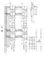
図1は本発明の実施の形態1のメモリモジュールの構造の一例を示す図であり、(a)は平面図、(b)は側面図、(c)は(a)のA−A断面を示す断面図、図2は図1(c)の断面図におけるB部を拡大して示す拡大部分断面図、図3は図1に示すメモリモジュールのブロック回路図の一例、図4は図1に示すメモリモジュールに実装されるウェハプロセスパッケージ(突起状端子半導体装置)の構造の一例を示す外観斜視図、図5は図1に示すメモリモジュールに実装されるSMD(リード端子を有する表面実装形の半導体装置であり、この半導体装置を以降、リード端子半導体装置という)とウェハプロセスパッケージの構造の一例を示す図であり、(a)はSMDの平面図、(b)はウェハプロセスパッケージの平面図、図6は図1に示すメモリモジュールに実装されるウェハプロセスパッケージの製造工程の一例を示すプロセスフロー、図7(a),(b),(c),(d),(e),(f)は図6に示すプロセスフローの主要工程に対応する半導体ウェハの構造の一例を示す拡大部分断面図、図8は図1に示すメモリモジュールに実装されるウェハプロセスパッケージとSMDのモジュール基板への実装手順の一例を示す基本実装フロー、図9は図1に示すメモリモジュールに実装されるウェハプロセスパッケージのモジュール基板への実装手順の一例を示す実装フロー、図10は図1に示すメモリモジュールに実装されるウェハプロセスパッケージのアンダーフィルにおける樹脂塗布方法の一例を示す拡大部分斜視図、図11は図10に示すアンダーフィルの樹脂塗布を行った際の樹脂の浸透経過の一例を示す図であり、(a),(c),(e),(g) は斜視図、(b),(d),(f),(h)は半導体チップを透過して示す平面図、図12および図13は本発明の実施の形態1のメモリモジュールの変形例の構造を示す平面図、図14は本発明の実施の形態1のアンダーフィルにおける変形例の樹脂塗布を行った際の樹脂の浸透経過を示す図であり、(a),(c),(e),(g) は斜視図、(b),(d),(f),(h)は半導体チップを透過して示す平面図、図15は本発明の実施の形態1のメモリモジュールの変形例の構造を示す図であり、(a)は平面図、(b)は側面図、図16は図15に示すメモリモジュールの反り状態の一例を示す側面図、図17は本発明の実施の形態1のメモリモジュールの変形例の構造を示す平面図、図18は図17に示すメモリモジュールの反り状態の一例を示す側面図である。
【0023】
図1に示す本実施の形態1のメモリモジュール100は、外部端子として突起状端子を備えるとともに、前記突起状端子を介して実装され、かつ半導体チップ1のボンディング電極1aの設置ピッチよりも前記突起状端子の設置ピッチを広げる配線部が設けられた突起状端子半導体装置と、半導体チップ1を備えるとともに、外部端子としてアウタリード21を備え、かつ半導体チップ1のボンディング電極1aと電気的に接続されたアウタリード21を介して実装されるリード端子半導体装置であるTSOP(Thin Small Outline Package) 20と、前記突起状端子半導体装置とTSOP20とを支持するモジュール基板2とからなり、前記突起状端子半導体装置とTSOP20とが共に同時リフローによって実装され、両者がモジュール基板2に混載されているものである。
【0024】
ここで、前記突起状端子半導体装置は、外部端子として設けられた複数のバンプ電極11(突起状端子)がパッケージ本体13(半導体装置本体)のエリア内に配置されているとともに、半導体チップ1のボンディング電極1aの設置ピッチよりもバンプ電極11の設置ピッチを広げる配線部を有しているものである。
【0025】
また、前記リード端子半導体装置は、外部端子として設けられた複数のアウタリード21がパッケージ本体22(半導体装置本体)から突出して配置されているものである。
【0026】
なお、前記突起状端子半導体装置および前記リード端子半導体装置において半導体チップ1のボンディング電極1aは、例えば、アルミニウムなどによって形成された電極であり、ワイヤボンディングなどを行う際に、そのボンディングワイヤと電気的に接続される電極である。
【0027】
また、前記突起状端子半導体装置および前記リード端子半導体装置における外部端子とは、モジュール基板2などの実装基板に前記半導体装置を実装した際に、モジュール基板2側の接続電極と電気的に接続される端子である。
【0028】
ここで、本実施の形態1では、前記突起状端子半導体装置が、チップサイズの小形半導体装置であるウェハプロセスパッケージ(以降、略してWPPと呼ぶ)10の場合を例に取り上げて説明する。
【0029】
したがって、本実施の形態1のメモリモジュール100は、チップサイズの突起状端子半導体装置であるWPP10と、SMD(表面実装形パッケージ)部品で、かつリード端子半導体装置の一例であるTSOP20と、他のリード端子半導体装置の一例として不揮発性読み出し専用メモリであるEEPROM(Electrically Erasable Programmable Read Only Memory)5とがモジュール基板2に混載されているものである。
【0030】
ここで、WPP10は、図4に示すように、外部端子として突起状端子であるバンプ電極11を備えるとともに、バンプ電極11を介してモジュール基板2に実装され、かつ半導体チップ1のエリア内においてボンディング電極1aの設置ピッチよりもバンプ電極11の設置ピッチを広げる配線部である再配線12が設けられた突起状端子半導体装置である。
【0031】
WPP10にバンプ電極11を用いると、バンプ電極11は高さのばらつきが小さいため、基板に実装した際の実装不良が少なくてすみ、その結果、実装歩留りが向上する。また、バンプ電極11は、実装高さが約0.13mmであり、実装高さを小さくできる。
【0032】
なお、図1に示すように、メモリモジュール100には、WPP10、TSOP20、EEPROM5の他に、キャパシタ3、小形の面付け抵抗4などの他の電子部品が搭載されている。
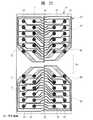
【0033】
つまり、本実施の形態1のメモリモジュール100には、その表裏面の一方の面に、18個のWPP10と、2つのTSOP20と、18個のキャパシタ3と、36個の小形の面付け抵抗4と、1つのEEPROM5とが搭載されており、さらに、その反対側の他方の面にも18個のWPP10が搭載されている。
【0034】
また、本実施の形態1のメモリモジュール100のWPP10は、モジュール基板2の一方の面において、2つのTSOP20を挟んでその両側に一列に合計18個(TSOP20を挟んで一方の側に10個、その反対側に8個)が配置されている。
【0035】
なお、2つのTSOP20は、その一方(図1において向かって上側に配置されたTSOP20)が周波数制御手段であるPLL(Phase-Locked Loop)6であり、また、他方(図1において向かって下側に配置されたTSOP20)がレジスタ機能を備えたレジスタ8である。
【0036】
つまり、本実施の形態1のメモリモジュール100では、PLL6およびレジスタ8もリード端子半導体装置である。
【0037】
なお、各WPP10に対応してその近傍に1つずつキャパシタ3が配置されている。
【0038】
さらに、各WPP10に対応して2つずつ合計36個の小形の面付け抵抗4が一列に配置されている。小形の面付け抵抗4は、メモリモジュール100のI/Oに対応して設けられるため、本実施の形態1のメモリモジュール100では片面に36個のI/Oが設けられていることにより、面付け抵抗4も36個搭載されている。小形の36個の面付け抵抗4は、モジュール基板2の外部端子である接続端子2aの近傍に、この接続端子2aにほぼ沿った状態で1列に配置されている。
【0039】
なお、図1(a)に示すように、メモリモジュール100のモジュール基板2の大きさは、例えば、L=133.35mm、M=38.1mmであり、図1(b)に示すように、実装高さ(Max)は、N=4mmである。
【0040】
また、本実施の形態1のメモリモジュール100において、TSOP20とWPP10とは同時リフローによって実装されたものであるが、図2に示すように、WPP10は、リフロー後、アンダーフィルによって樹脂封止され、これにより、封止部14が形成されている。
【0041】
すなわち、WPP10のパッケージ本体13とモジュール基板2との間のバンプ電極11の周囲が樹脂封止され、そこに封止部14が形成されている。
【0042】
なお、図1に示すメモリモジュール100は、WPP10をDRAMとして用いたものであるとともに、エラーコードコレクション付き72bit幅バスのモジュール基板2を用いたものである。
【0043】
したがって、メモリモジュール100は、モジュール基板2の表裏両面に合計36個のDRAM(WPP10)が搭載されたモジュールであり、例えば、64Mbit(16M×4)のDRAMとすると、16ワード×72bit×2バンク構成のDRAMモジュールである。
【0044】
ここで、図3は、図1に示すメモリモジュール100のブロック回路図であり、16ワード×72bit×2バンク構成のDRAMモジュールのブロック回路図である。
【0045】
図3において、1バンクめのRS0系とRS2系とが同時に動作する構造となっており、かつ、2バンクめのRS1系とRS3系とが同時に動作する構造となっており、1バンクめもしくは2バンクめをレジスタ8によってバンクセレクトし、1バンクめを読み出す時は、2バンクめは読み出さず、同様に、2バンクめを読み出す時は、1バンクめは読み出さない。
【0046】
なお、レジスタ8のA端子〔S0 to S3〕が、1バンクめおよび2バンクめの何れかのDRAM(WPP10)のチップセレクト(CS)端子と接続され、レジスタ8がバンクを選択することににより、選択された半導体チップ1のCS端子への入力となる。
【0047】
また、各チップのD0〜D35が36個の各WPP10を示しており、各チップにおける〔I(Input)/O(Output)0 to I/O3〕端子が独立端子としてモジュール基板2の接続端子2aに接続されている。
【0048】
また、全てのDRAMを合わせて、データとして使用するI/Oが、DQ0からDQ63まで64bitあり、またチェックとして使用するI/Oが、CB0からCB7まで8bitあり、両者を合計して72bitの2バンク構成となる。
【0049】
なお、図3に示す各端子に示した記号について説明すると、〔A0 to A11〕はアドレス入力、〔DQ0 to DQ63〕はデータ入出力、〔CB0to CB7〕はチェックビット(データ入出力)、〔S0 to S3〕はチップセレクト入力、〔RE〕はローイネーブル(RAS)入力、〔CE〕はコラムイネーブル(CAS)入力、〔W〕はライトイネーブル入力、〔DQMB0to DQMB7〕はバイトデータマスク、〔CK0 to CK3〕はクロック入力、〔CKE0〕はクロックイネーブル入力、〔WP〕はSerial PD用のライトプロテクト、〔REGE〕はレジスタイネーブル、〔SDA〕はSerial PD用のデータ入出力、〔SCL〕はSerial PD用のクロック入力、〔SA0 to SA2〕はシリアルアドレス入力、〔Vcc〕は高電位側電源、〔Vss〕はグランド、〔NC〕はノンコネクトをそれぞれ示す。
【0050】
次に、WPP10の詳細構造について説明すると、図4に示すように、WPP10の半導体チップ1のボンディング電極1aから外部端子である半田のバンプ電極11までを再配線12によって電気的に接続した構造となっている。
【0051】
すなわち、狭ピッチで配置されたボンディング電極1aに対し、これと電気的に接続されるバンプ電極11のピッチを、再配線12によって広げたものである。
【0052】
これは、ウェハ単位で素子の機能部位を形成し、その後、ダイシングを行って各半導体チップ1に個片化することにより、チップサイズのパッケージとするものである。
【0053】
したがって、SMD(表面実装形)部品のパッケージと同様の製造方法によって組み立てられる小形パッケージと比較しても低コストで効率よく製造できる。
【0054】
なお、図5にSMD部品の一例であるTSOP20と、チップサイズの突起状端子半導体装置の一例であるWPP10とを示し、その大きさの差を示す。
【0055】
図5(a)は、図1に示すメモリモジュール100に実装されるTSOP20を示した平面図であり、また、図5(b)は、同様に、図1に示すメモリモジュール100に実装されるWPP10を示した平面図である。
【0056】
図5に示すように、例えば、DRAMがTSOP20などのSMD(表面実装形)タイプのパッケージである場合と比較すると、WPP10の方がインナリードやアウタリード21を備えていない分、小形化することができる。
【0057】
したがって、本実施の形態1のメモリモジュール100のように、WPP10によるDRAMをモジュール基板2に実装することにより、個片処理で形成されるTSOP20よりも大幅に実装面積を減らすことが可能となる。
【0058】
すなわち、WPP10として実装することにより、その半導体チップ1を実装する限り最も少ない面積に実装することができ、その結果、モジュール容量を大幅に増加させることができる。
【0059】
なお、ベアチップ実装となるフリップチップ実装においても同様の容量を実現することが可能ではあるが、フリップチップ実装では再配線12が形成されないため、外部端子の設置ピッチが狭く、SMDタイプの部品と同時にリフロー実装することができない。これにより、ベアチップ実装部品では、フリップチップボンダを用いて1個ずつ実装しなければならず、WPP10の方が実装効率も高い。
【0060】
つまり、WPP10の実装では、前記フリップチップボンダなどの特殊実装装置を必要としないため、実装における工程を少なくすることができる。
【0061】
また、WPP10は、外部端子であるバンプ電極11の設置ピッチを、フリップチップ実装より広いピッチで実装可能なため、モジュール基板2における配線ルールを広くすることができる。したがって、モジュール基板2のコスト高を招くことなく、これにより、コストを抑えた高密度実装のメモリモジュール100を実現することができる。
【0062】
さらに、WPP10では、半導体チップ1のボンディング電極1aから外部端子であるバンプ電極11までの配線距離を、TSOP20などのSMD部品におけるボンディング電極1aからアウタリード21先端までの距離より短い距離の配線で結ぶことが可能になるため、高速の信号伝達に対応することができる。
【0063】
これにより、メモリモジュール100において高速化対応が可能となり、その結果、高速バス対応を実現できる。
【0064】
ここで、本実施の形態1のメモリモジュール100において、これに実装される全ての半導体装置(パッケージ)をWPP10にしない理由、すなわち、チップサイズの突起状端子半導体装置の一例であるWPP10と、SMD部品(本実施の形態1ではTSOP20)とを混載する理由について説明する。
【0065】
WPP10は、前工程ウェハ処理によって形成されるものである。したがって、従来の後工程でデバイス1つ1つを形成する工程に関しても全てウェハ単位で処理される。
【0066】
この場合、1枚のウェハ内の良品数が少なければ、不良品に対して加工を行うことになり、コスト高となる。
【0067】
その結果、半導体ウェハの歩留りが十分高まっていない品種では、コストメリットが無い。
【0068】
また、品種ごとに露光用レチクルを準備する必要があるので、大量生産しない製品に関しては、リードフレームに対して組み付ける半導体装置(パッケージ)の方が汎用性のある部品材料を利用できる。これにより、大量生産しない製品は、WPP10にしない方が良い。
【0069】
さらに、物理的条件も重要であり、取り出し端子数とチップサイズの関係により、小チップで取り出し端子数の多いロジックなどもWPP10にしない方がよい。これは、ボンディング電極1aから再配線12を形成した後の電極パッド(図7に示す拡散防止接着層7c)およびバンプ電極11が設置できないためである。
【0070】
したがって、WPP10にした方が良いデバイスは、歩留りが高く、ウェハ当たりのチップ取得数が多いチップ、特に、小形メモリデバイスである。
【0071】
これに対し、WPP10にしがたいデバイスは、歩留りが低く、ウェハ当たりのチップ取得数が少ないチップ、特に、大形チップ、先端デバイスもしくは少量生産しか行わないデバイスなどがある。また、チップ面積の割りに外部端子数の多いASIC(Application Specific Integrated Circuit)などでは、WPP10にした場合、バンプ電極11の設置ピッチを十分広く取れない場合があり、このような場合も従来のパッケージとした方が実装が容易になる。
【0072】
続いて、図6に示すWPP10(図1参照)のプロセスフローおよび図7に示す前記プロセスフローの主要工程に対応するウェハ断面図を用いてWPP10の製造方法について説明する。
【0073】
まず、図6に示すステップS1により、ウェハ前工程処理を行う。これにより、図7(a)に示すシリコン基板7の主面にボンディング電極1aを露出させて無機絶縁保護膜7aを形成する。
【0074】
続いて、ステップS2により、WPP−第一絶縁層形成を行う。すなわち、図7(b)に示すように、シリコン基板7の無機絶縁保護膜7a上にポリイミドやフッ素樹脂などからなる第一絶縁層7bを形成する。
【0075】
その後、ステップS3により、WPP−再配線層形成を行う。すなわち、図7(c)に示すように、第一絶縁層7b上に、ボンディング電極1aと電気的に接続させて再配線12を形成する。
【0076】
さらに、ステップS4により、WPP−第二絶縁層形成を行う。すなわち、図7(d)に示すように、再配線12上にポリイミドやエポキシなどからなる第二絶縁層7dを形成する。
【0077】
その後、ステップS5により、WPP−UBM(アンダーバンプメタル)形成を行う。すなわち、図7(e)に示すように、再配線12と電気的に接続させてUBMである拡散防止接着層7cを形成する。
【0078】
続いて、ステップS6により、ウェハ検査(W検)を行う。これは、半導体ウェハ(シリコン基板7)のスクライブエリアに形成された電極パッドにプローブ針を当てて、ウェハ処理が仕様通りに行われているか否かを電気的特性によって検査するものである。
【0079】
その後、ステップS7により、シリコン基板7のプローブ検査(P検1)を行う。これは、シリコン基板7のボンディング電極1aにプローブ針を当てて、半導体チップ1の各電気的動作が正しいか否かを検査して不良箇所を検出するものである。
【0080】
さらに、ステップS8により、不良箇所に対して救済、すなわちレーザ救済を行う。これは、レーザによって冗長回路のヒューズを切断して不良箇所を救済するものである。
【0081】
その後、ステップS9により、プローブ検査(P検2)を行う。これは、前記P検1で救済した不良箇所が修正されているか否かを確認するものである。
【0082】
続いて、ステップS10により、ウェハ裏面マーキングを行ってシリコン基板7の裏面に所定のマークを付す。
【0083】
さらに、ステップS11により、バンプ形成を行う。すなわち、図7(f)に示すように、再配線12上のボンディング電極1aから引き出した端部に設けられたUBMである拡散防止接着層7c上にWPP10の外部端子であるバンプ電極11(突起状端子)を形成する。
【0084】
ここで、バンプ電極11は、例えば、印刷法によって形成される。ウェハ(シリコン基板7)上のバンプ形成位置に対応したメタルマスクを配置し、はんだペーストを塗り込み、前記メタルマスクをはずした後一括リフローすることによって、前記ウェハ上のバンプ電極11が一度に形成される。
【0085】
その後、ステップS12により、ダイシングを行って半導体ウェハすなわちシリコン基板7を切断し、その結果、図4に示すようなWPP10を形成する。
【0086】
その後、ステップS13により、WPP10のエージングすなわちバーンイン(BI)テストを行う。
【0087】
さらに、ステップS14により、単品選別を行って良品のWPP10を選別する。
【0088】
これにより、WPP10の組み立てを完了する。
【0089】
なお、図6に示す製造手順では、ステップS9に示すプローブ検査(P検2)を行った後、シリコン基板7の裏面を研磨するバックグラインディング(以降、BGと略す)工程を行わない場合を説明したが、ステップS9のプローブ検査(P検2)の工程からステップS10のウェハ裏面マーキングの工程に移る間にBG工程を行ってもよい。
【0090】
ここで、BG工程は、シリコン基板7の裏面を研磨してシリコン基板7を薄くし、これによって形成されるWPP10の高さを低くするものである。
【0091】
すなわち、WPP10の薄形化を目的としてこれが有する半導体チップ1を薄くするものである。
【0092】
したがって、BG工程を行うことにより、WPP10の実装高さを低くすることが可能になる(例えば、1mm以下にできる)。
【0093】
さらに、BG工程を行うことにより、シリコン基板7の厚さを薄くできるため、シリコン基板7においてチップ取り数増加のためダイシング時のスクライブ巾を狭くした際にもダイシング時の冷却水のスクライブ溝への浸入を妨げることなく、ダイシングできる。
【0094】
これにより、ダイシング時のシリコン基板7の損傷を防ぐことができ、シリコン基板7の歩留りを向上できる。これは、直径が300mmのシリコン基板7をダイシングする際に、特に有効的である。
【0095】
また、図6に示す製造手順のステップS6〜ステップS9に示す工程(ウェハ検査(W検)、プローブ検査(P検1)、レーザ救済、プローブ検査(P検2))を、ステップS1のウェハ前工程処理工程と、ステップS2のWPP−第一絶縁層形成工程との間で行ってもよい。
【0096】
すなわち、ステップS1に示すウェハ前工程後に、ステップS6〜ステップS9に示す工程を行うものである。
【0097】
これにより、シリコン基板7に絶縁膜を形成する前に、一連のプローブ検査を行うことができ、ボンディング電極1aが損傷した際にもその損傷を残さずにWPP10を組み立てることができる。
【0098】
次に、図8および図9を用いて、本実施の形態1の図1に示すメモリモジュール100の製造方法について説明する。
【0099】
なお、図1に示すメモリモジュール100は、モジュール基板2の表裏両面にWPP10を実装し、かつ片方の面にTSOP20を実装したものである。
【0100】
まず、図6に示すプロセスフローに基づいてWPP10を製造する。
【0101】
すなわち、外部端子としてバンプ電極11(突起状端子)を備えるとともに、半導体チップ1のエリア内においてボンディング電極1aの設置ピッチよりもバンプ電極11の設置ピッチを広げる再配線12(配線部)が設けられた図4に示すチップサイズのWPP10(突起状端子半導体装置)をウェハ前工程処理によって形成し、これを準備する(ここでは、18×2=36個準備する)。
【0102】
なお、本実施の形態1では、WPP10が有する半導体チップ1は、DRAMである。
【0103】
一方、このWPP10の他に、モジュール基板2に搭載するSMD部品であるリード端子半導体装置を組み立てて準備する。
【0104】
ここでは、半導体チップ1のボンディング電極1aと電気的に接続された外部端子であるアウタリード21を備えたリード端子半導体装置である2つのTSOP20(そのうち1つはPLL6で、他の1つはレジスタ8)と、EEPROM5(リード端子半導体装置)と、36×2=72個の小形の面付け抵抗4をそれぞれ準備する。
【0105】
なお、図8に示す部品実装の基本フローに基づいて大凡の実装手順について説明する。
【0106】
まず、ステップS15により、モジュール基板2へのはんだ印刷を行い、リード端子半導体装置のアウタリード21の先端やWPP10のバンプ電極11などと電気的に接続するための端子(ランドパッド)を形成する。
【0107】
その後、ステップS16により、SMD搭載を行うとともに、ステップS17により、WPP10搭載を行う。
【0108】
続いて、ステップS18により、一括リフローを行い、これにより、リード端子半導体装置のアウタリード21と前記ランドパッドとを、かつWPP10のバンプ電極11と前記ランドパッドとを電気的に接続する。
【0109】
その後、ステップS19により洗浄を行う。ただし、洗浄は行わなくてもよい。
【0110】
さらに、ステップS20により、アンダーフィルによる樹脂封止を行う。
【0111】
次に、図9に示す詳細の実装フローを用いてメモリモジュール100の製造方法を詳しく説明する。
【0112】
まず、図9に示すステップS21により、モジュール基板2の所定箇所にはんだ印刷を行う。
【0113】
続いて、ステップS22により、モジュール表面搭載を行う。ここでは、モジュール基板2の表面にそれぞれ所定数のWPP10(18個)、TSOP20(2個)、小形の面付け抵抗4(36個)およびEEPROM5(1個)を搭載機によって配置する。
【0114】
その後、ステップS23により、モジュール基板2の表面側の全ての前記部品を一括した(同時に)はんだリフローによって実装する。
【0115】
その後、ステップS24により、モジュール裏面搭載を行う。ここでは、表面側と同じ方法でモジュール基板2の裏面に各部品を搭載機によって配置する。
【0116】
続いて、ステップS25により、モジュール基板2の裏面側の全ての前記部品を一括した(同時に)はんだリフローによって実装する。
【0117】
これにより、モジュール基板2の表裏両面にそれぞれ所定数のWPP10(18×2個)、TSOP20(2個)、小形の面付け抵抗4およびEEPROM5を実装(混載)したメモリモジュール100を組み立てることができる。
【0118】
その後、ステップS26により、洗浄を行う。
【0119】
ただし、洗浄は、行わなくてもよい。
【0120】
その後、ステップS27により、モジュールテストを行う。すなわち、メモリモジュール100の所定の検査を行って不良チップを検出する。
【0121】
続いて、ステップS28に示す不良チップリペアを行って不良チップの交換を行う。その際、再加熱を行ってはんだを溶融し、不良チップ(不良の半導体装置)を取り外して良品チップ(良品の半導体装置)と取り替える。
【0122】
その後、ステップS29により、再び、リフローを行って全ての部品を実装する。
【0123】
続いて、ステップS30により、洗浄を行う。
【0124】
ただし、洗浄は、行わなくてもよい。
【0125】
その後、ステップS31に示すアンダーフィルによる樹脂封止をWPP10に対して行う。アンダーフィルは、DRAMの様にチップサイズが比較的大きく、その結果、バンプ電極11への応力緩衝機能が不十分なWPP10の場合に、WPP10のパッケージ本体13とモジュール基板2との間に樹脂9を充填し、バンプ電極11に加わる応力を低減するものである。
【0126】
すなわち、アンダーフィルは、WPP10におけるパッケージ本体13とモジュール基板2との間の樹脂封止であり、バンプ電極11の周囲を樹脂9によって固めて保護するものである。
【0127】
なお、アンダーフィルを行う際には、液状の樹脂9を図10に示すディスペンサ60のノズル60aからモジュール基板2の片面ずつに対して塗布する。すなわち、モジュール基板2の表裏面のWPP10に対してその片面ずつ樹脂9を塗布する。
【0128】
両面の塗布が終了した段階で、モジュール基板2の表裏面を一括加熱してその表裏面の樹脂9を同時に硬化させる。すなわち、樹脂9の両面への塗布が終了した後、雰囲気加熱などにより、両面を同時にキュアベーク(硬化)する。
【0129】
その後、図9に示すステップS32により、ケーシングを行って、さらに、ステップS33により、モジュール最終テストを行う。
【0130】
なお、EEPROM5には、専用ライタによって所定の情報を書き込む。
【0131】
これにより、図1に示すメモリモジュール100の組み立てを完了する。
【0132】
ここで、WPP10の実装と同じ実装面積となるベアチップ実装について両実装の比較のための説明をする。
【0133】
まず、ベアチップ実装では、ボンディング電極1aを再配線12によって再配置せずに実装基板に実装するため、外部端子の設置ピッチが狭く、実装基板の配線ルールが厳しくなり、実装基板のコストが高くなる。そのうえ、モジュール組み立ての際、他のSMD部品実装のためのはんだリフロー実装工程の他に処理速度が比較的遅いフリップチップボンダを使用する実装工程を追加しなければならない。
【0134】
したがって、本実施の形態1のメモリモジュール100におけるWPP10方が、その実装において、前記ベアチップ実装よりも多くの効果(フリップチップボンダなどの特殊実装装置を使用しないため、実装工程を少なくできる)が得られる。
【0135】
次に、本実施の形態1のメモリモジュール100の製造方法におけるアンダーフィルの方法について説明する。
【0136】
図10は、図1に示すメモリモジュール100に実装されるWPP10のアンダーフィルにおける樹脂塗布方法を示す図であり、また、図11は図10に示す塗布方法で樹脂9を塗布した際の樹脂9の浸透経過を示した図である。
【0137】
図10において、各矢印は、ノズル60aの進行方向を表しており、この矢印に沿ってディスペンサ60およびノズル60aがWPP10の短辺上を移動していく。
【0138】
本実施の形態1の樹脂塗布方法では、平面形状が長方形のWPP10の短辺方向に沿ってディスペンサ60を断続的に、かつほぼ直線的に移動させ、WPP10の上方からノズル60aを介して各WPP10の短辺に対して順次樹脂9を滴下していく。つまり、1つのWPP10の塗布を終了したらノズル60aを次のWPP10の短辺上の手前側の端部に移動させ、そこでノズル60aを一端停止させる。
【0139】
その後、WPP10の短辺の手前側端部から向う側端部までノズル60aを移動させながら樹脂9を滴下し、そこで一端ノズル60aの移動と樹脂9の滴下とを停止する。
【0140】
続いて、樹脂9の滴下を停止させた状態で、これの隣に配置されたWPP10の短辺の手前側端部にノズル60aを移動させ、そこから同様にして樹脂9の滴下を行うとともに、順次、各WPP10のアンダーフィルを行っていく。
【0141】
なお、図11は、図10に示す塗布方法で、バンプ電極11の配置が15行×4列でDRAMのWPP10に樹脂9を塗布した際の樹脂9の濡れ広がりの状態を示したものであり、図11(a),(b)は、短辺塗布直後、図11(c),(d)は、塗布後所定時間(少)経過後、図11(e),(f)は、塗布後所定時間(大)経過後、図11(g),(h)は、塗布後所定時間(大)経過後に周辺にフィレット9aを形成するため、ノズル60aを一周させて樹脂9を塗布した状態を示したものである。
【0142】
図11(e),(f)に示すように、樹脂9がWPP10とモジュール基板2との間全体に濡れ広がった後、再び、ディスペンサ60およびノズル60aをWPP10のパッケージ本体13の周に周回させて図11(g)に示すフィレット9aを確実に形成し、これによって、WPP10がモジュール基板2に固定される強度を一層高めても良い。
【0143】
次に、図12は本発明の実施の形態1のメモリモジュール100の変形例であるメモリモジュール200の構造を示したものである。
【0144】
メモリモジュール200は、モジュール基板2の片面において、18個のWPP10(突起状端子半導体装置)が等ピッチ間隔で一列に並んで実装され、WPP10の近傍に1つのTSOP20(リード端子半導体装置)が実装された場合の一例であり、一列に並んで配置されたWPP10の中央付近にTSOP20(リード端子半導体装置)が配置されている。
【0145】
すなわち、1つのTSOP20の両側に一列に並んで複数(10個と8個)のWPP10が配置されている。
【0146】
さらに、モジュール基板2においてその外部端子である接続端子2a側にリード端子半導体装置であるSOP(Small Outline Package)61(レジスタ8)が9個並んで実装され、かつ接続端子2aと反対側(接続端子2aから遠い側)に18個のWPP10が実装され、それぞれのWPP10にはアンダーフィルが行われている。
【0147】
このような実装形態のメモリモジュール200において、WPP10のアンダーフィル用の樹脂9を塗布する際には、一列に配置された18個のWPP10の短辺に対してほぼ直線的に樹脂9を塗布する。
【0148】
これにより、効率良く樹脂9を塗布できる。
【0149】
また、図13は本発明の実施の形態1のメモリモジュール100の変形例であるメモリモジュール300の構造を示したものである。
【0150】
図13に示すメモリモジュール300では、そのモジュール基板2において、18個のWPP10が、2つずつまたは2行×2列マトリクス配置の4つずつを1つの群(塊)として実装されている。
【0151】
さらに、それぞれのWPP10が、その長手方向をメモリモジュール300のモジュール基板2の短辺方向に平行にして実装されている。
【0152】
ここでは、このようなWPP10の実装状態でWPP10のアンダーフィルを行う際に効率よく行う樹脂9の塗布方法を説明する。
【0153】
つまり、樹脂9の塗布温度が比較的低い場合、WPP10のパッケージ本体13の長辺側に樹脂9を塗布した方がパッケージ本体13とモジュール基板2との間に樹脂9が浸透していく距離が短い。その結果、塗布時間の短縮化を図ることができる。
【0154】
したがって、各パッケージ本体13の少なくとも片側の長辺に沿っては、ノズル60aを移動させるスペースを確保することが望ましく、高密度実装の観点からは、ノズル60aをさせない側の長辺は、他の部品とできるだけ接近させて配置することが望ましい。
【0155】
これを利用し、半導体チップ1が多bit構成で、かつメモリモジュール300の同一I/Oに多数のDRAMから結線される場合に、同一面内の2×2組のDRAMをなるべく近づけた配置の際の塗布方法とした時に効果が大きい。
【0156】
したがって、図13に示すようなWPP10の実装状態において、樹脂9をそれぞれのWPP10の外側長辺に沿ってその外側長辺外周に対して塗布することが好ましく、この塗布方法を用いて2×2組のDRAM(WPP10)の外側長辺に沿って樹脂9を塗布した場合、塗布対象のパッケージ本体13とは反対側の塗布対象外のパッケージ本体13に樹脂9が流れたり、もしくは、樹脂9が、いずれかに漏れ広がったりすることを防ぐことができる。
【0157】
なお、メモリモジュール300では、I/Oが(×4)構成のものを4個集めて16bit構成とし、これを一群として実装する方が好ましい。したがって、図13に示すWPP10の実装形態においては、その矢印のような塗布軌跡で樹脂9を塗布することが好ましい。
【0158】
次に、図14は、他の変形例の樹脂塗布を行った際の樹脂9の浸透経過を示す図である。
【0159】
つまり、図15に示すようなメモリモジュール400のWPP10の実装形態において、アンダーフィルの樹脂9を、図14に示すようにパッケージ本体13の対向する2辺外周部に対して塗布するものであり、ここでは、各WPP10の両短辺側においてその一方の端から反対側の端まで樹脂9を塗布する。
【0160】
なお、図14(a),(b)に示す矢印は、ディスペンサ60の移動軌跡を示しており、図14(c),(d)は、両短辺(2辺)塗布直後、図14(e),(f)は、塗布後所定時間(中)経過後、図14(g),(h)は、塗布後所定時間(大)経過後の樹脂9の浸透状態をそれぞれ示したものである。
【0161】
本実施の形態1では、樹脂9の浸透の最終段階においても、両短辺から浸透した樹脂9同士は互いに分離した状態にあり、中間に樹脂9の浸透していない領域が存在する。パッケージ本体13とモジュール基板2との熱膨張差や、モジュール基板2の反り変形によってバンプ電極11に作用する応力は、パッケージ本体13の中心からの距離が大きくなるにしたがって増加し、角部のバンプ電極11において最大となる。したがって、長方形のパッケージ本体13の両短辺近傍に樹脂9が浸透していれば、中間に浸透していない領域が存在しても、ある程度のバンプ電極11の応力低減効果を得ることができる。
【0162】
これにより、パッケージ本体13の全面に塗布する場合に近い効果をより少ない樹脂9とより少ない作業時間で得ることができる。
【0163】
すなわち、塗布時間の短縮と、塗布量の低減とを図ることが可能になる。
【0164】
また、パッケージ本体13の4角に樹脂9を塗布するだけでもよく、その際には、最外周に配置されたバンプ電極11への応力を低減し、その結果、バンプ電極11の接続寿命を延ばすことができる。
【0165】
次に、図15(a),(b)は、メモリモジュール100の変形例であるメモリモジュール400の構造を示したものであり、モジュール基板2の片面において16個のWPP10が等ピッチ間隔で一列に実装され、このメモリモジュール400において、アンダーフィル用の樹脂9を一列に配置された16個のWPP10に対して直線的に塗布するものである。図15(a)に示す矢印は、ディスペンサ60(図10参照)の移動軌跡を示すものである。
【0166】
また、図16は、図15に示すメモリモジュール400が反って撓んだ状態を示したものである。これは、メモリモジュール400の検査などを行う際のソケット挿入時に、モジュール基板2の端部を押さえた時などにおいて起こり得る状態である。
【0167】
すなわち、図16に示すように、図15に示すメモリモジュール400がその長手方向に反って撓んだ際、隣あったWPP10の封止部14が相互に接触することなく一体化していなければ、メモリモジュール400は、全体に亘って撓むため、応力はメモリモジュール400全体にほぼ均一に分散される。
【0168】
これにより、外部からの荷重にも耐え得る構造とすることができ、その結果、メモリモジュール400の信頼性を向上できる。
【0169】
さらに、図17、図18に示すメモリモジュール500は、モジュール基板2の複数の接続端子2aの配列方向に沿って16個のWPP10が4つの領域に各4つずつに分割されて実装され、1つの領域の4つのWPP10における封止部14が繋がって形成されているものである。
【0170】
すなわち、WPP10をある群(塊)ごとに分けて実装し、それらが群単位にアンダーフィルの封止部14によって繋がると、そのメモリモジュール500の群(塊)の箇所の剛性は、見かけ上、WPP10をも含むものとなって高くなる。
【0171】
これにより、モジュール基板2の曲げ応力は、WPP10の群と群の間の間隙に集中する。
【0172】
すなわち、WPP10同士の間隔など、アンダーフィルの樹脂9の塗布に影響を及ぼす因子如何で隣同士の封止部14が繋がる場合もあり、その場合でも図17および図18に示すメモリモジュール500のように、部分的に繋がらない非実装部2bを有することにより、外力が加わった際にも、この非実装部2bが撓んでWPP10のバンプ電極11の接続部や半導体チップ1に応力が掛かることを防ぐことができる。
【0173】
その結果、前記応力を分散できるため、メモリモジュール500のWPP10における接続信頼性を向上できる。
【0174】
なお、本実施の形態1のメモリモジュール100,200,300,400,500においては、WPP10がアンダーフィル封止されているため、チップ全面もしくは主要部がより強固に固着され、その結果、耐衝撃性を向上させることができるとともに、耐湿性も向上できる。
【0175】
ここで、モジュール製品においては、高密度実装を実現する他の手段としてTCP(Tape Carrier Package) の積層実装などがある。ただし、この技術では、チップ薄形化によってチップクラックが発生することがある。これに対し、本実施の形態1のメモリモジュール100,200,300,400,500においては、アンダーフィルによるチップ固着によって耐衝撃性を向上させることができるため、前記チップクラックの発生も防止することができる。
【0176】
さらに、WPP10がアンダーフィル封止され、かつ半導体チップ1の主面と反対側の面(背面)が露出した状態でモジュール基板2に実装されるとともに、アンダーフィル封止により半導体チップ1の前記主面の全面もしくはその主要部がモジュール基板2と固着されるため、熱抵抗を低くすることができる。
【0177】
その結果、メモリモジュール100,200,300,400,500の放熱性を向上できるとともに、長寿命化を図ることができる。
【0178】
(実施の形態2)
図19は本発明の実施の形態2のメモリモジュールの構造の一例を示す平面図である。
【0179】
本実施の形態2のメモリモジュール600は、72個のDRAMであるWPP10(突起状端子半導体装置)が行列のマトリクス配置によって実装され、かつそれぞれのWPP10に対しての入出力信号の接続を、2行(図19のメモリモジュール600においては、モジュール基板2の短辺に平行な方向を行、これと直角な方向を列とするが、行列の関係はこれと反対であってもよい)ごとの合計8つとECC用の1つの合計9つのWPP10の群(塊)を1群として、各群ごとに切換える9個のメモリ選択手段であるFET(Field Effect Transistor)−バススイッチ15(リード端子半導体装置)が各群のWPP10に対応して実装されている。
【0180】
つまり、メモリモジュール600においては、2行分の9個のWPP10に対しての入出力信号の接続を、これに対応した1つのFET−バススイッチ15によってその1群(8個)の中で切換えるものであり、モジュール基板2の接続端子2aの数を増加させずにWPP10の数を増加させるものである。
【0181】
したがって、メモリモジュール600では、実施の形態1のメモリモジュール100と比較してその4倍の数のWPP10を搭載している。
【0182】
すなわち、メモリモジュール600は、FET−バススイッチ15によってI/Oを個別に切り換え可能なようにして、より多数のDRAMを実装できるようにしたものである。
【0183】
なお、メモリモジュール600におけるFET−バススイッチ15は、その外観形状が、例えば、リード端子半導体装置の一例であるSOPタイプのものである。
【0184】
本実施の形態2のメモリモジュール600のその他の構造およびメモリモジュール600の製造方法については、前記実施の形態1のメモリモジュール100のものと同じであるため、その重複説明は省略する。
【0185】
(実施の形態3)
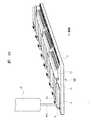
図20は本発明の実施の形態3のメモリモジュールの構造の一例を示す図であり、(a)は平面図、(b)は側面図、図21は図20に示すメモリモジュールのブロック回路図の一例、図22は図20に示すメモリモジュールに実装されるウェハプロセスパッケージ(突起状端子半導体装置)の構造の一例を示す底面図、図23は図20(a)に示すメモリモジュールのC部におけるモジュール基板の配線の一例を示す基板側配線図、図24、図25および図26は本発明の実施の形態3のメモリモジュールにおけるウェハプロセスパッケージのバンプ配置の変形例とそれに対応する基板側配線の変形例の配線図、図27は図25に示すウェハプロセスパッケージのバンプ配置と基板側配線の変形例の他の変形例を示すバンプ配置および配線図である。
【0186】
図20(a),(b)に示す本実施の形態3のメモリモジュール700は、8バイトの168ピンのUnbuffered SDRAM(スタティックDRAM)−DIMM(Dual In-line Memory Module) に、片面8個のWPP10(突起状端子半導体装置)と、小形の面付け抵抗4と、キャパシタ3と、EEPROM5とを混載したものである。
【0187】
ただし、メモリモジュール700には、図1のメモリモジュール100に搭載されているレジスタ8は搭載されていない。
【0188】
なお、図21は、図20に示すメモリモジュール700のブロック回路図の一例を示したものであり、2バンク構成を示している。
【0189】
ここで、図21に示す各端子に示した記号の説明については、実施の形態1のメモリモジュール100のブロック回路図で説明したものと同じであるため、その重複説明は省略する。
【0190】
図21に示すメモリモジュール700においては、1バンクめのS0系と、2バンクめのS1系との何れを読み出すかは、レジスタ8が搭載されていないため、ダイレクトの信号によって行う。つまり、Unbufferedタイプであるため、ダイレクトに何れかのバンクに信号が入り、何れかのバンクの半導体チップ1をセレクトする。
【0191】
なお、各チップのD0〜D15が両面16個の各WPP10を示しており、各チップにおける〔I/O0 to I/O3〕端子が独立端子としてモジュール基板2の接続端子2aに接続されている。
【0192】
また、全てのDRAMを合わせて、データとして使用するI/Oが、DQ0からDQ63まで64bitあり、これらが2バンク構成となっている。
【0193】
図20に示すメモリモジュール700は、図1に示すメモリモジュール100と比較して廉価タイプのモジュールである。
【0194】
また、メモリモジュール700のモジュール基板2の大きさは、例えば、P=133.35mm、Q=33.02mmであり、図20(b)に示すように、実装高さ(Max)は、R=4mmである。
【0195】
なお、図20(a)に示すように、メモリモジュール700では、その片面において8個のDRAMであるWPP10(突起状端子半導体装置)が一列に配置され、さらに、隣あったWPP10の間または横においてその長手方向の中央付近に対応した箇所にキャパシタ3(コンデンサ)が配置されている。
【0196】
これは、WPP10とキャパシタ3との間の配線長を最短にするためのものである。
【0197】
ここで、メモリモジュール700に用いられるWPP10の構造を図22に示す。
【0198】
図22に示すWPP10の半導体チップ1では、その長手方向の中央付近にバンプ電極11を配置させない空き領域1bが形成されている。
【0199】
これは、空き領域1bが形成されるように再配線12によってバンプ電極11の設置ピッチを一部変更したものであり、WPP10の長手方向の中央付近にバンプ電極11を設置しない空き領域1bを設けたものである。
【0200】
なお、図23は、図20(a)のC部におけるモジュール基板2の基板側配線を示したものである。
【0201】
図22および図23に示すように、半導体チップ1の空き領域1bに隣接させてキャパシタ3(リード端子半導体装置)が実装され、キャパシタ3の電源用配線2cがモジュール基板2の半導体チップ1の空き領域1bに対向した表層に表層配線2hとして形成されている(ただし、内層に内層配線2gとして形成されていてもよい)。
【0202】
つまり、図22に示すように、半導体チップ1の長手方向の中央付近にバンプ電極11を設置しない空き領域1bを形成しているため、WPP10の信号線をモジュール基板2のチップ中央部に対応した箇所に出さなくても結線を行うことができ、その結果、キャパシタ3をWPP10に最も近づけて実装できる。
【0203】
これにより、WPP10とキャパシタ3との間の配線長が最短となって動作特性を向上できる。
【0204】
なお、モジュール基板2は、図23に示すように、コア2層のVccとGnd層および片面2層ずつの信号線の合計6層のメタル層によって形成されており、WPP10のバンプ電極11が接続される表面層のランド2dからアドレス・機能系などの共通配線2eは、一層下の層にビアホール2fを経由して接続し、これにより、モジュール基板2の長手方向に延びる内層配線2gに接続している。
【0205】
また、I/O配線は、モジュール基板2の表層配線2hを介して近くに配置された接続端子2aに接続される。したがって、ビアホール2fを経由することによるインダクタンス増加を回避できる。
【0206】
なお、図23に示す配線では、Vss(Gnd)やVddをキャパシタ3(コンデンサ)から横方向に延ばして形成しているが、すぐコア層にビアホール2fを経由して接続してもよい。
【0207】
次に、図24、図25および図26は、実施の形態3のメモリモジュール700におけるWPP10のバンプ配置の変形例とそれに対応する基板側配線の変形例の配線を示した図であり、図27は図25に示すウェハプロセスパッケージのバンプ配置と基板側配線の変形例の他の変形例を示すものである。
【0208】
なお、図24、図25、図26および図27におけるWPP10は、複数のWPP10においてWPP10相互に共通して配線接続可能なアドレス、機能、電源およびGndなどの共通電極群である共通バンプ電極群(共通突起状端子群)1cと、WPP10ごとに独立して配線接続されるI/Oなどの独立電極群である独立バンプ電極群(独立突起状端子群)1dとがそれぞれのWPP10上において区分されて設けられた場合である。
【0209】
さらに、WPP10において独立バンプ電極群1dがそのパッケージ本体13の短辺側の片側端部に配置されており、メモリモジュール700の片面では、8個のWPP10が、それぞれの独立バンプ電極群1dをモジュール基板2の接続端子2a側に向けて実装されている。
【0210】
これにより、モジュール基板2には、8個のWPP10の共通バンプ電極群1cを接続する配線である共通配線2eが表層配線2hによって形成されている。
【0211】
ここでは、共通バンプ電極群1c、すなわちアドレス系、機能系のバンプ電極11の設置ピッチを広く設け、特にパッケージ本体13の長手方向に直角な方向にバンプ電極間を通り抜けて配線が多く形成可能なように、チップ長手方向に設置ピッチを大きく形成する。
【0212】
さらに、独立バンプ電極群1d、すなわちI/O系のバンプ電極11の設置ピッチは狭くしてパッケージ本体13の片側外周に配置する。
【0213】
これにより、表層配線2hのみによって共通配線2eを形成できるため、モジュール基板2における配線層数を削減できる。
【0214】
なお、図24に示すWPP10では、再配線12によって、その共通バンプ電極群1cを個々に規則性を持たせて、かつパッケージ本体13に対して斜めに配置している。
【0215】
これによれば、アドレス、機能、電源およびGndなどの共通電極を接続する複数の共通配線2eをパッケージ本体13の長手方向に対して平行に形成することができる。
【0216】
その結果、モジュール基板2における配線密度を最も高くすることができ、さらに、共通配線2eの距離を最短にすることができる。
【0217】
また、WPP10のバンプ電極11の数がチップサイズに対して比較的少ない時や、モジュール基板2がアディティブ基板などのように配線ルールが細かい基板の場合には、表面層と内層のGndおよびVccの層の一部を信号層として使用することにより、4層のモジュール基板2を製造することができ、これを用いてメモリモジュール700を組み立てることができる。
【0218】
この場合、I/O系の独立配線2iを接続端子2a側に設けられたバンプ電極11から接続し、かつアドレス、機能、電源およびGndなどの共通電極を接続する複数の共通配線2eをチップ同士の間を通るように形成できる。
【0219】
また、図25に示すWPP10では、再配線12(図22参照)によって、その共通バンプ電極群1cを格子状に配置している。その際、図22に示すように、再配線12をチップ内部の電源・Gnd分配として使用し、1つのバンプ電極11と複数のボンディング電極1aとを再配線12によって電気的に接続することにより、バンプ電極11の数を減らすことができる(外部端子数を低減できる)。
【0220】
なお、図25に示す基板側配線では、モジュール基板2の表層のみによって結線しており、バンプ電極11の配置は傾斜させていないため、基板側配線の屈曲や傾斜を利用して配線している。
【0221】
また、図26に示すWPP10は、図25に示したWPP10のバンプ配列よりも多少バンプ電極11の設置ピッチを広げて設置したものであり、これをモジュール基板2上で、それの長手方向もしくは短辺方向に傾斜させて配列させたものである。
【0222】
これにより、モジュール基板2側の共通配線2eをパッケージ本体13の長手方向と傾斜させた関係にすることができ、その結果、図24に示した共通配線2eと同様に、共通配線2eを直線で形成することができる。
【0223】
また、図27は、図25に示すWPP10のバンプ配列よりも多少バンプ電極11の設置ピッチを広げて設置した他の変形例である。この変形例では、I/O系以外の独立ピンも下から引き出す構成となっている。ビット構成の専用化をすることによってピン数を減らし、これにより、共通配線2eの間隔を大きく形成して、I/Oピンとそれ以外の独立ピンは狭ピッチとした例である(図27に示すd1>d2)。
【0224】
図27に示す変形例の効果としては、共通配線同士の間隔を広くしたため、ピン間により多くの配線を引き回すことができる。したがって、モジュール基板2上の配線が、表層配線2hのみによって共通化できるため、モジュール基板2の内層配線2g(図23参照)を必要としない。なお、I/Oピンと電源などの独立ピンは狭ピッチとしたが、これらはピン間に配線を引き回さず、単独で下に、すなわち接続端子2aに配線を取り出すため、狭いピッチでもよい。
【0225】
図27においては、Dの配線レイアウトにした場合、ピン間を3つの表層配線2hが通ることとなり、また、Eの配線レイアウトにした場合、ピン間を4つの表層配線2hが通ることとなる。
【0226】
なお、図24、図25、図26および図27では、モジュール基板2上の配線密度を極限まで高めるため、モジュール基板2の実装ランドは敢えて示さず、共通配線2eと直交したスリット状のレジスト開口部を疑似的なはんだ接続ランドとした。
【0227】
本実施の形態3のメモリモジュール700のその他の構造およびメモリモジュール700の製造方法については、前記実施の形態1のメモリモジュール100のものと同じであるため、その重複説明は省略する。
【0228】
以上、本発明者によってなされた発明を発明の実施の形態に基づき具体的に説明したが、本発明は前記発明の実施の形態に限定されるものではなく、その要旨を逸脱しない範囲で種々変更可能であることは言うまでもない。
【0229】
例えば、前記実施の形態1,2および3のメモリモジュール100〜700にでは、EEPROM5をアウタリード21を有したリード端子半導体装置として用いる場合を説明したが、不揮発性読み出し専用メモリであるEEPROM5を突起状端子半導体装置すなわちWPP10と同様の構造として形成し、これを実装してもよい。
【0230】
ただし、その際、WPP構造のEEPROM5は、アンダーフィルによる封止を行わず、DRAMのWPP10のみにアンダーフィルを行う。
【0231】
すなわち、WPP構造のEEPROM5はモジュール基板2から取り外し自在に実装する。
【0232】
これは、EEPROM5の製品歩留りは低く、電気的書き込みを行った時点で不良が発見された場合に、EEPROM5のみを良品と置き換えることができるようにするためである。EEPROM5の場合は、チップ寸法がDRAMに比べて小さいため、バンプ電極11に加わる応力が小さく、アンダーフィルなしでも十分な信頼性を得ることができる。WPP構造のEEPROM5を実装することにより、SOPタイプの場合より実装面積を少なくすることができるとともに、コスト面においても、SOPタイプより安くすることができる。
【0233】
また、前記実施の形態1,2および3では、モジュール基板2の表裏両面にWPP10が実装されている両面実装タイプのメモリモジュールについて説明したが、前記メモリモジュールは、片面実装タイプのものであってもよい。
【0234】
さらに、WPP10(突起状端子半導体装置)と混載されるリード端子半導体装置については、TSOP20に限られるものではなく、TSOP20以外のQFP(Quad Flat Package)やTCP(Tape Carrier Package) などの半導体装置であってもよい。
【0235】
また、前記実施の形態1,2および3では、突起状端子半導体装置がWPP10の場合について説明したが、前記突起状端子半導体装置は、その外部端子がバンプ電極11で、かつ半導体チップ1のボンディング電極1aの設置ピッチよりもバンプ電極11の設置ピッチを広げる配線部を備えた半導体装置であれば、他の半導体装置であってもよい。
【0236】
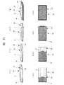
そこで、図28、図29および図30に、前記突起状端子半導体装置のWPP10以外の変形例を示す。
【0237】
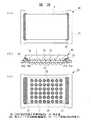
図28(a),(b),(c)は、前記突起状端子半導体装置の変形例としてCSP(Chip Scale Package) 30を示したものである。
【0238】
なお、CSP30は、半導体チップ1とほぼ同じか、もしくはそれより若干大きい程度のチップサイズのものであり、エラストマ31を介在させてテープ基板32によって半導体チップ1を支持するファンイン構造のものである。
【0239】
さらに、外部端子として半田などからなる複数のバンプ電極34(突起状端子)が半導体チップ1のエリア内領域に設けられ、テープ基板32に設けられた接続リード32aと半導体チップ1のボンディング電極1aとが電気的に接続され、かつ半導体チップ1のボンディング電極1aの設置ピッチよりもバンプ電極34の設置ピッチを広げる配線部である端子ピッチ拡張配線32bがテープ基板32に形成されている。
【0240】
なお、半導体チップ1のボンディング電極1a上には封止部33が形成されている。
【0241】
図29(a),(b) は、前記突起状端子半導体装置の変形例としてチップフェイスアップ搭載方式のBGA(Ball Grid Array)40を示したものである。
【0242】
なお、BGA40は、BGA基板42にダイボンド材45を介してフェイスアップ方式で半導体チップ1が固着されたものであり、半導体チップ1のボンディング電極1aとBGA基板42の基板電極42fとが金などからなるボンディングワイヤ41によって電気的に接続されている。
【0243】
さらに、外部端子として半田などからなる複数のバンプ電極44(突起状端子)がBGA基板42の裏面側に格子状配列で設けられるとともに、半導体チップ1のボンディング電極1aの設置ピッチよりもバンプ電極44の設置ピッチを広げる配線部である端子ピッチ拡張配線42aがBGA基板42に形成されている。
【0244】
なお、端子ピッチ拡張配線42aには、信号配線42b、GNDプレーン42c、Vddプレーン42dおよびスルーホール42eなどが含まれている。
【0245】
また、半導体チップ1やボンディングワイヤ41などを樹脂封止するモールド部43が形成されている。
【0246】
図30(a),(b),(c)は、前記突起状端子半導体装置の変形例としてチップフェイスダウン搭載方式のBGA(Ball Grid Array)50を示したものである。
【0247】
なお、BGA50は、BGA基板52に小形バンプ51を介してフェイスダウン方式で半導体チップ1が搭載されたフリップチップ構造のものであり、半導体チップ1のボンディング電極1aとBGA基板52の電極とが小形バンプ51によって電気的に接続されている。
【0248】
さらに、外部端子として半田などからなるバンプ電極54(突起状端子)がBGA基板52の裏面側に格子状配列で設けられるとともに、半導体チップ1のボンディング電極1a(図29参照)の設置ピッチよりもバンプ電極54の設置ピッチを広げる配線部である端子ピッチ拡張配線52a(図30(c)参照)がBGA基板52に形成されている。
【0249】
なお、半導体チップ1とBGA基板52との間すなわち小形バンプ51の周囲がアンダーフィルによって樹脂封止され封止部53が形成されている。
【0250】
図28に示すCSP30、図29に示すBGA40および図30に示すBGA50においても、半導体チップ1のボンディング電極1aの設置ピッチよりもバンプ電極34,44,54の設置ピッチを広げる配線部である端子ピッチ拡張配線32b,42a,52aがそれぞれに設けられているため、これらをモジュール基板2などに実装する際にはリフロー実装を行うことができる。
【0251】
【発明の効果】
本願によって開示される発明のうち、代表的なものによって得られる効果を簡単に説明すれば、以下のとおりである。
【0252】
(1).メモリモジュールにおいて突起状端子半導体装置をモジュール基板に実装することにより、個片処理で形成される半導体チップを有したリード端子半導体装置よりも大幅に実装面積を減らすことが可能となる。これにより、半導体チップを実装する限り最も少ない面積に実装することができ、その結果、モジュール容量を大幅に増加させることができる。
【0253】
(2).突起状端子半導体装置としてWPPを実装することにより、外部端子であるバンプ電極の設置ピッチをフリップチップ実装より広いピッチで実装可能なため、モジュール基板における配線ルールを広くすることができる。これにより、コストを抑えた高密度実装のメモリモジュールを実現することができる。
【0254】
(3).半導体チップのボンディング電極から外部端子であるWPPのバンプ電極までをTSOPなどのSMD部品より短い距離の配線で結ぶことが可能になる。これにより、メモリモジュールにおいて高速化対応が可能となり、その結果、高速バス対応を実現できる。
【0255】
(4).メモリモジュールにおいてWPPがアンダーフィル封止されていることにより、チップ全面がより強固に固着されるため、耐衝撃性を向上させることができる。これにより、チップクラックの発生も防止することができる。
【0256】
(5).WPPがアンダーフィル封止され、かつ半導体チップの背面が露出した状態でモジュール基板に実装されるとともに、アンダーフィル封止により半導体チップの主面の全面がモジュール基板と固着されるため、メモリモジュールにおける熱抵抗を低くすることができる。その結果、メモリモジュールの放熱性を向上できるとともに、その長寿命化を図ることができる。
【図面の簡単な説明】
【図1】(a),(b),(c)は本発明の実施の形態1のメモリモジュールの構造の一例を示す図であり、(a)は平面図、(b)は側面図、(c)は(a)のA−A断面を示す断面図である。
【図2】図1(c)の断面図におけるB部を拡大して示す拡大部分断面図である。
【図3】図1に示すメモリモジュールのブロック回路図の一例である。
【図4】図1に示すメモリモジュールに実装されるウェハプロセスパッケージ(突起状端子半導体装置)の構造の一例を示す外観斜視図である。
【図5】(a),(b)は図1に示すメモリモジュールに実装されるSMD(リード端子半導体装置)とウェハプロセスパッケージの構造の一例を示す図であり、(a)はSMDの平面図、(b)はウェハプロセスパッケージの平面図である。
【図6】図1に示すメモリモジュールに実装されるウェハプロセスパッケージの製造工程の一例を示すプロセスフローである。
【図7】(a),(b),(c),(d),(e),(f)は図6に示すプロセスフローの主要工程に対応する半導体ウェハの構造の一例を示す拡大部分断面図である。
【図8】図1に示すメモリモジュールに実装されるウェハプロセスパッケージとSMDのモジュール基板への実装手順の一例を示す基本実装フローである。
【図9】図1に示すメモリモジュールに実装されるウェハプロセスパッケージのモジュール基板への実装手順の一例を示す実装フローである。
【図10】図1に示すメモリモジュールに実装されるウェハプロセスパッケージのアンダーフィルにおける樹脂塗布方法の一例を示す拡大部分斜視図である。
【図11】(a),(b),(c),(d),(e),(f),(g),(h)は図10に示すアンダーフィルの樹脂塗布を行った際の樹脂の浸透経過の一例を示す図であり、(a),(c),(e),(g) は斜視図、(b),(d),(f),(h)は半導体チップを透過して示す平面図である。
【図12】本発明の実施の形態1のメモリモジュールの変形例の構造を示す平面図である。
【図13】本発明の実施の形態1のメモリモジュールの変形例の構造を示す平面図である。
【図14】(a),(b),(c),(d),(e),(f),(g),(h)は本発明の実施の形態1のアンダーフィルにおける変形例の樹脂塗布を行った際の樹脂の浸透経過を示す図であり、(a),(c),(e),(g) は斜視図、(b),(d),(f),(h)は半導体チップを透過して示す平面図である。
【図15】(a),(b) は本発明の実施の形態1のメモリモジュールの変形例の構造を示す図であり、(a)は平面図、(b)は側面図である。
【図16】図15に示すメモリモジュールの反り状態の一例を示す側面図である。
【図17】本発明の実施の形態1のメモリモジュールの変形例の構造を示す平面図である。
【図18】図17に示すメモリモジュールの反り状態の一例を示す側面図である。
【図19】本発明の実施の形態2のメモリモジュールの構造の一例を示す平面図である。
【図20】(a),(b) は本発明の実施の形態3のメモリモジュールの構造の一例を示す図であり、(a)は平面図、(b)は側面図である。
【図21】図20に示すメモリモジュールのブロック回路図の一例である。
【図22】図20に示すメモリモジュールに実装されるウェハプロセスパッケージ(突起状端子半導体装置)の構造の一例を示す底面図である。
【図23】図20に示すメモリモジュールのC部におけるモジュール基板の配線の一例を示す基板側配線図である。
【図24】本発明の実施の形態3のメモリモジュールにおけるウェハプロセスパッケージのバンプ配置の変形例とそれに対応する基板側配線の変形例の配線図である。
【図25】本発明の実施の形態3のメモリモジュールにおけるウェハプロセスパッケージのバンプ配置の変形例とそれに対応する基板側配線の変形例の配線図である。
【図26】本発明の実施の形態3のメモリモジュールにおけるウェハプロセスパッケージのバンプ配置の変形例とそれに対応する基板側配線の変形例の配線図である。
【図27】図25に示すウェハプロセスパッケージのバンプ配置と基板側配線の変形例の他の変形例を示すバンプ配置および配線図である。
【図28】(a),(b),(c)は本発明のメモリモジュールに実装される突起状端子半導体装置の変形例であるCSPの構造を示す図であり、(a)は平面図、(b)は断面図、(c)は底面図である。
【図29】(a),(b) は本発明のメモリモジュールに実装される突起状端子半導体装置の変形例であるチップフェイスアップ搭載方式のBGAの構造を示す図であり、(a)は外観斜視図、(b)は断面図である。
【図30】(a),(b),(c)は本発明のメモリモジュールに実装される突起状端子半導体装置の変形例であるチップフェイスダウン搭載方式のBGAの構造を示す図であり、(a)は平面図、(b)は断面図、(c)は底面図である。
【符号の説明】
1 半導体チップ
1a ボンディング電極
1b 空き領域
1c 共通バンプ電極群(共通突起状端子群)
1d 独立バンプ電極群(独立突起状端子群)
2 モジュール基板
2a 接続端子(外部端子)
2b 非実装部
2c 電源用配線
2d ランド
2e 共通配線
2f ビアホール
2g 内層配線
2h 表層配線
2i 独立配線
3 キャパシタ
4 面付け抵抗
5 EEPROM(不揮発性読み出し専用メモリ)
6 PLL(周波数制御手段)
7 シリコン基板
7a 無機絶縁保護膜
7b 第一絶縁層
7c 拡散防止接着層
7d 第二絶縁層
8 レジスタ
9 樹脂
9a フィレット
10 WPP(突起状端子半導体装置)
11 バンプ電極(突起状端子)
12 再配線(配線部)
13 パッケージ本体(半導体装置本体)
14 封止部
15 FET−バススイッチ(メモリ選択手段)
20 TSOP(リード端子半導体装置)
21 アウタリード(外部端子)
22 パッケージ本体(半導体装置本体)
30 CSP(突起状端子半導体装置)
31 エラストマ
32 テープ基板
32a 接続リード
32b 端子ピッチ拡張配線(配線部)
33 封止部
34 バンプ電極(突起状端子)
40 BGA(突起状端子半導体装置)
41 ボンディングワイヤ
42 BGA基板
42a 端子ピッチ拡張配線(配線部)
42b 信号配線
42c GNDプレーン
42d Vddプレーン
42e スルーホール
42f 基板電極
43 モールド部
44 バンプ電極(突起状端子)
45 ダイボンド材
50 BGA(突起状端子半導体装置)
51 小形バンプ
52 BGA基板
52a 端子ピッチ拡張配線(配線部)
53 封止部
54 バンプ電極(突起状端子)
60 ディスペンサ
60a ノズル
61 SOP(リード端子半導体装置)
100,200,300,400,500,600,700 メモリモジュール[0001]
BACKGROUND OF THE INVENTION
The present invention relates to a semiconductor manufacturing technique, and more particularly to a technique effective when applied to high-density mounting of semiconductor chips in a memory module.
[0002]
[Prior art]
The technology described below has been studied by the present inventors in researching and completing the present invention, and the outline thereof is as follows.
[0003]
An example of a module product on which a plurality of semiconductor devices are mounted is a memory module.
[0004]
In this memory module, a plurality of semiconductor devices having memory chips are mounted on one side or both sides of a module substrate. When a memory to be used is installed in a personal computer or workstation, the personal computer or workstation It is mounted on a mother board provided in and mounted with memory in units of modules.
[0005]
Therefore, as a semiconductor device mounted on a memory module, a semiconductor chip is sealed with a resin, such as TSOP (Thin Small Outline Package) or TCP (Tape Carrier Package), and the sealing formed by this resin sealing is used. A surface mount type semiconductor device called SMD (Surface Mount Devices) having a lead terminal (external terminal) for drawing out an electrode to the outside of the stop portion is used.
[0006]
As module products, for example, those having various structures are disclosed in, for example, Japanese Patent Laid-Open Nos. 10-209368, 1-258466, and 7-86492.
[0007]
Japanese Laid-Open Patent Publication No. 10-209368 describes a CPU (Central Processing Unit) module. Japanese Laid-Open Patent Publication No. 1-258466 describes a memory module on which an SMD component having a DRAM (Dynamic Random Access Memory) chip is mounted. Further, Japanese Patent Application Laid-Open No. 7-86492 describes a technique for applying an underfill resin in an MCM (Multi-Chip-Module).
[0008]
[Problems to be solved by the invention]
However, the SMD component mounted on the memory module of the above-described technology has a structure in which the package size is larger than the chip size due to the influence of the sealed package body (semiconductor device body) and the outer lead. .
[0009]
As a result, there is a problem that the number of semiconductor chips that can be mounted on the module substrate is limited.
[0010]
Another problem is that it is difficult to design a memory module having a high-speed interface to cope with a high-speed CPU due to the effect of inductance added by sealing.
[0011]
SUMMARY OF THE INVENTION An object of the present invention is to provide a memory module and a method for manufacturing the same that improve the mounting density of semiconductor chips to increase module capacity and realize high-speed bus compatibility.
[0012]
The above and other objects and novel features of the present invention will be apparent from the description of this specification and the accompanying drawings.
[0013]
[Means for Solving the Problems]
Of the inventions disclosed in this application, the outline of typical ones will be briefly described as follows.
[0014]
In other words, the memory module of the present invention includes a protruding terminal as an external terminal, and is mounted via the protruding terminal, and a wiring portion that extends the installation pitch of the protruding terminal more than the installation pitch of the bonding electrode of the semiconductor chip is provided. A protruding terminal semiconductor device provided, an outer lead as an external terminal, and mounted via the outer lead electrically connected to the bonding electrode of the semiconductor chip, and the protruding terminal semiconductor A module substrate supporting the device and the lead terminal semiconductor device, wherein the protruding terminal semiconductor device and the lead terminal semiconductor device are mounted together, and both are mixedly mounted on the module substrate.
[0015]
Furthermore, the memory module of the present invention includes a projecting terminal as an external terminal and is mounted via the projecting terminal, so that the installation pitch of the projecting terminal is wider than the installation pitch of the bonding electrodes in the area of the semiconductor chip. A chip-sized protruding terminal semiconductor device provided with a rewiring as a wiring portion, and an outer lead as an external terminal and mounted via the outer lead electrically connected to the bonding electrode of the semiconductor chip A terminal semiconductor device; and a module substrate supporting the protruding terminal semiconductor device and the lead terminal semiconductor device, wherein the protruding terminal semiconductor device and the lead terminal semiconductor device are mounted together, both of which are the module It is mixed on the substrate.
[0016]
Therefore, since the lead terminal semiconductor device and the protruding terminal semiconductor device are mixedly mounted, the protruding terminal semiconductor device can be mounted with a mounting area similar to that of the semiconductor chip.
[0017]
As a result, the semiconductor chip can be mounted in the smallest area as long as the semiconductor chip is mounted. Therefore, the mounting density of the semiconductor chip can be improved.
[0018]
As a result, the module capacity in the memory module can be increased.
[0019]
Also, the method of manufacturing a memory module according to the present invention includes a protruding terminal semiconductor provided with a protruding terminal as an external terminal, and provided with a wiring portion that expands the installation pitch of the protruding terminal more than the installation pitch of the bonding electrodes of the semiconductor chip. A step of preparing a device, a step of preparing a lead terminal semiconductor device including an outer lead which is an external terminal electrically connected to the bonding electrode of the semiconductor chip, and the protruding terminal semiconductor device and the lead terminal semiconductor A step of disposing a device on a module substrate, and a step of simultaneously reflowing the protruding terminal semiconductor device and the lead terminal semiconductor device and mounting them on the module substrate. And the lead terminal semiconductor device are mixedly mounted on the module substrate.
[0020]
Furthermore, in the method for manufacturing a memory module of the present invention, the rewiring, which is a wiring portion that includes a protruding terminal as an external terminal and widens the installation pitch of the protruding terminal more than the installation pitch of the bonding electrode in the area of the semiconductor chip. Providing a chip-shaped protruding terminal semiconductor device provided; preparing a lead terminal semiconductor device including an outer lead that is an external terminal electrically connected to the bonding electrode of the semiconductor chip; and A step of disposing the protruding terminal semiconductor device and the lead terminal semiconductor device on a module substrate; a step of simultaneously reflowing the protruding terminal semiconductor device and the lead terminal semiconductor device and mounting them on the module substrate; The projecting terminal semiconductor device and the lead terminal semiconductor device are connected to the module base. It is intended to mixed in.
[0021]
DETAILED DESCRIPTION OF THE INVENTION
Hereinafter, embodiments of the present invention will be described in detail with reference to the drawings.
[0022]
(Embodiment 1)
1A and 1B are diagrams showing an example of the structure of a memory module according to
[0023]
The
[0024]
Here, in the protruding terminal semiconductor device, a plurality of bump electrodes 11 (projecting terminals) provided as external terminals are arranged in the area of the package body 13 (semiconductor device body) and the
[0025]
In the lead terminal semiconductor device, a plurality of
[0026]
In the protruding terminal semiconductor device and the lead terminal semiconductor device, the
[0027]
The protruding terminal semiconductor device and the external terminal in the lead terminal semiconductor device are electrically connected to the connection electrode on the
[0028]
In the first embodiment, the case where the protruding terminal semiconductor device is a wafer process package (hereinafter abbreviated as WPP) 10 which is a chip-sized small semiconductor device will be described as an example.
[0029]
Therefore, the
[0030]
Here, as shown in FIG. 4, the
[0031]
When the
[0032]
As shown in FIG. 1, in addition to the
[0033]
That is, in the
[0034]
Further, the
[0035]
One of the two TSOPs 20 (the
[0036]
That is, in the
[0037]
One
[0038]
Further, a total of 36
[0039]
As shown in FIG. 1A, the size of the
[0040]
In the
[0041]
That is, the periphery of the
[0042]
The
[0043]
Therefore, the
[0044]
Here, FIG. 3 is a block circuit diagram of the
[0045]
In FIG. 3, the first bank RS0 system and the RS2 system operate simultaneously, and the second bank RS1 system and the RS3 system operate simultaneously. When the second bank is bank-selected by the
[0046]
The A terminal [S0 to S3] of the
[0047]
Further, D0 to D35 of each chip indicate 36
[0048]
In addition, for all DRAMs, the I / O used as data is 64 bits from DQ0 to DQ63, and the I / O used as a check is 8 bits from CB0 to CB7. Bank configuration.
[0049]
3 will be described. [A0 to A11] is an address input, [DQ0 to DQ63] is a data input / output, [CB0 to CB7] is a check bit (data input / output), [S0 to S3] is a chip select input, [RE] is a row enable (RAS) input, [CE] is a column enable (CAS) input, [W] is a write enable input, [DQMB0to DQMB7] is a byte data mask, [CK0 to CK3] is a clock input, [CKE0] is a clock enable input, [WP] is a write protect for Serial PD, [REGE] is a register enable, [SDA] is a data input / output for Serial PD, and [SCL] is a Serial PD. Clock input, [SA0 to SA2] is serial Address input, [Vcc] of the high potential power source, [Vss] denotes respectively ground, [NC] are non-connection.
[0050]
Next, the detailed structure of the
[0051]
That is, the pitch of the
[0052]
In this method, a functional part of an element is formed in a wafer unit, and then dicing is performed to separate each
[0053]
Therefore, even when compared with a small package assembled by the same manufacturing method as the package of SMD (surface mount type) parts, it can be efficiently manufactured at a low cost.
[0054]
FIG. 5 shows a
[0055]
FIG. 5A is a plan view showing the
[0056]
As shown in FIG. 5, for example, the
[0057]
Therefore, by mounting the DRAM based on
[0058]
That is, by mounting as the
[0059]
In flip chip mounting, which is bare chip mounting, the same capacitance can be realized. However, since the
[0060]
That is, the mounting of the
[0061]
In addition, since the
[0062]
Further, in the
[0063]
As a result, it is possible to cope with high speed in the
[0064]
Here, in the
[0065]
The
[0066]
In this case, if the number of non-defective products in one wafer is small, the defective product will be processed, resulting in high cost.
[0067]
As a result, there is no cost merit in a product type in which the yield of semiconductor wafers is not sufficiently increased.
[0068]
Further, since it is necessary to prepare an exposure reticle for each type, a semiconductor device (package) assembled to a lead frame can use a more versatile component material for products that are not mass-produced. As a result, products that are not mass-produced should not be made WPP10.
[0069]
Furthermore, physical conditions are also important, and it is better not to use
[0070]
Therefore, a device that should be made WPP10 is a chip with a high yield and a large number of chip acquisitions per wafer, particularly a small memory device.
[0071]
On the other hand, devices that are difficult to achieve with the
[0072]
Next, a method for manufacturing
[0073]
First, wafer pre-process processing is performed by step S1 shown in FIG. Thus, the inorganic insulating
[0074]
Subsequently, in step S2, WPP-first insulating layer formation is performed. That is, as shown in FIG. 7B, a first insulating
[0075]
Then, WPP-rewiring layer formation is performed by step S3. That is, as shown in FIG. 7C, the
[0076]
Further, in step S4, WPP-second insulating layer formation is performed. That is, as shown in FIG. 7D, a second insulating
[0077]
Then, WPP-UBM (under bump metal) formation is performed by step S5. That is, as shown in FIG. 7E, the diffusion preventing
[0078]
Subsequently, in step S6, wafer inspection (W inspection) is performed. In this method, a probe needle is applied to an electrode pad formed in a scribe area of a semiconductor wafer (silicon substrate 7), and whether or not the wafer processing is performed as specified is inspected based on electrical characteristics.
[0079]
Thereafter, in step S7, the probe inspection (P inspection 1) of the
[0080]
Further, in step S8, the defective portion is relieved, that is, laser relieved. In this method, a defective portion is relieved by cutting a fuse of a redundant circuit with a laser.
[0081]
Thereafter, a probe test (P test 2) is performed in step S9. This is to confirm whether or not the defective portion remedied by the
[0082]
Subsequently, in step S10, wafer back surface marking is performed to attach a predetermined mark to the back surface of the
[0083]
Furthermore, bump formation is performed by step S11. That is, as shown in FIG. 7F, a bump electrode 11 (protrusion) that is an external terminal of the
[0084]
Here, the
[0085]
Thereafter, in step S12, dicing is performed to cut the semiconductor wafer, that is, the
[0086]
Thereafter, in step S13, aging of the
[0087]
Further, in step S14, single item sorting is performed to sort out
[0088]
Thereby, the assembly of the
[0089]
In the manufacturing procedure shown in FIG. 6, after performing the probe inspection (P inspection 2) shown in step S9, the back grinding (hereinafter abbreviated as BG) step of polishing the back surface of the
[0090]
Here, in the BG process, the back surface of the
[0091]
That is, the
[0092]
Therefore, by performing the BG process, it becomes possible to reduce the mounting height of the WPP 10 (for example, 1 mm or less).
[0093]
Furthermore, since the thickness of the
[0094]
Thereby, damage of the
[0095]
Further, the steps (wafer inspection (W inspection), probe inspection (P inspection 1), laser relief, probe inspection (P inspection 2)) shown in steps S6 to S9 of the manufacturing procedure shown in FIG. You may perform between a pre-process process and a WPP-first insulating layer formation process of step S2.
[0096]
That is, the processes shown in steps S6 to S9 are performed after the wafer pre-process shown in step S1.
[0097]
As a result, a series of probe inspections can be performed before the insulating film is formed on the
[0098]
Next, a method for manufacturing the
[0099]
Note that the
[0100]
First, the
[0101]
In other words, the bump electrode 11 (projection terminal) is provided as an external terminal, and the rewiring 12 (wiring portion) is provided in the area of the
[0102]
In the first embodiment, the
[0103]
On the other hand, in addition to the
[0104]
Here, there are two TSOPs 20 (one of which is a
[0105]
A general mounting procedure will be described based on the basic flow of component mounting shown in FIG.
[0106]
First, in step S15, solder printing is performed on the
[0107]
Thereafter, SMD mounting is performed in step S16, and
[0108]
Subsequently, in step S18, batch reflow is performed, whereby the
[0109]
Thereafter, cleaning is performed in step S19. However, it is not necessary to perform cleaning.
[0110]
Furthermore, resin sealing by underfill is performed in step S20.
[0111]
Next, the manufacturing method of the
[0112]
First, solder printing is performed on a predetermined portion of the
[0113]
Then, module surface mounting is performed by step S22. Here, a predetermined number of WPPs 10 (18 pieces), TSOP 20 (two pieces), small imposition resistors 4 (36 pieces) and EEPROM 5 (one piece) are arranged on the surface of the
[0114]
Thereafter, in step S23, all the components on the surface side of the
[0115]
Then, module backside mounting is performed by step S24. Here, each component is arranged on the back surface of the
[0116]
Subsequently, in step S25, all the components on the back side of the
[0117]
As a result, it is possible to assemble a
[0118]
Thereafter, cleaning is performed in step S26.
[0119]
However, the cleaning may not be performed.
[0120]
Thereafter, a module test is performed in step S27. That is, a predetermined inspection of the
[0121]
Subsequently, defective chip repair is performed in step S28 to replace the defective chip. At that time, reheating is performed to melt the solder, and the defective chip (defective semiconductor device) is removed and replaced with a non-defective chip (defective semiconductor device).
[0122]
Thereafter, in step S29, reflow is performed again to mount all components.
[0123]
Subsequently, cleaning is performed in step S30.
[0124]
However, the cleaning may not be performed.
[0125]
Then, resin sealing by underfill shown in step S31 is performed on the
[0126]
In other words, the underfill is a resin seal between the
[0127]
When underfilling is performed, the
[0128]
When the application of both surfaces is completed, the front and back surfaces of the
[0129]
Then, casing is performed by step S32 shown in FIG. 9, and a module final test is further performed by step S33.
[0130]
Note that predetermined information is written into the
[0131]
Thereby, the assembly of the
[0132]
Here, a description will be given for comparison between the two mountings of the bare chip mounting having the same mounting area as the mounting of the
[0133]
First, in the bare chip mounting, the
[0134]
Therefore, the
[0135]
Next, an underfill method in the method for manufacturing the
[0136]
FIG. 10 is a view showing a resin application method in the underfill of the
[0137]
In FIG. 10, each arrow represents the traveling direction of the
[0138]
In the resin coating method of the first embodiment, the
[0139]
Thereafter, the
[0140]
Subsequently, in a state where the dripping of the
[0141]
FIG. 11 shows the state of wet spreading of the
[0142]
As shown in FIGS. 11 (e) and 11 (f), after the
[0143]
Next, FIG. 12 shows the structure of a
[0144]
In the
[0145]
That is, a plurality (10 and 8) of
[0146]
Further, nine SOP (Small Outline Package) 61 (registers 8) as lead terminal semiconductor devices are mounted side by side on the
[0147]
In the
[0148]
Thereby, the
[0149]
FIG. 13 shows the structure of a
[0150]
In the
[0151]
Further, each
[0152]
Here, a method of applying the
[0153]
That is, when the application temperature of the
[0154]
Therefore, it is desirable to ensure a space for moving the
[0155]
By using this, when the
[0156]
Therefore, in the mounted state of the
[0157]
In the
[0158]
Next, FIG. 14 is a figure which shows the penetration | invasion progress of the
[0159]
That is, in the mounting form of the
[0160]
The arrows shown in FIGS. 14A and 14B indicate the movement trajectory of the
[0161]
In the first embodiment, even in the final stage of the penetration of the
[0162]
As a result, an effect close to that applied to the entire surface of the
[0163]
That is, it is possible to shorten the application time and reduce the application amount.
[0164]
In addition, the
[0165]
Next, FIGS. 15A and 15B show the structure of a
[0166]
FIG. 16 shows a state where the
[0167]
That is, as shown in FIG. 16, when the
[0168]
Thereby, it can be set as the structure which can also bear the load from the outside, As a result, the reliability of the
[0169]
Furthermore, the
[0170]
That is, when the
[0171]
Thereby, the bending stress of the
[0172]
In other words, the
[0173]
As a result, since the stress can be dispersed, the connection reliability of the
[0174]
In the
[0175]
Here, in module products, another means for realizing high-density mounting includes TCP (Tape Carrier Package) stacked mounting. However, in this technique, chip cracks may occur due to chip thinning. On the other hand, in the
[0176]
Further, the
[0177]
As a result, the heat dissipation of the
[0178]
(Embodiment 2)
FIG. 19 is a plan view showing an example of the structure of the memory module according to the second embodiment of the present invention.
[0179]
In the
[0180]
That is, in the
[0181]
Therefore, in the
[0182]
That is, the
[0183]
The FET-
[0184]
Since the other structure of the
[0185]
(Embodiment 3)
20 is a diagram showing an example of the structure of the memory module according to
[0186]
A
[0187]
However, the
[0188]
FIG. 21 shows an example of a block circuit diagram of the
[0189]
Here, the explanation of the symbols shown in each terminal shown in FIG. 21 is the same as that explained in the block circuit diagram of the
[0190]
In the
[0191]
D0 to D15 of each chip indicate 16
[0192]
Further, the I / O used as data for all DRAMs is 64 bits from DQ0 to DQ63, and these have a 2-bank configuration.
[0193]
A
[0194]
Further, the size of the
[0195]
As shown in FIG. 20A, in the
[0196]
This is for minimizing the wiring length between the
[0197]
Here, the structure of the
[0198]
In the
[0199]
This is a partial change in the installation pitch of the
[0200]
FIG. 23 shows the board-side wiring of the
[0201]
As shown in FIGS. 22 and 23, a capacitor 3 (lead terminal semiconductor device) is mounted adjacent to the
[0202]
That is, as shown in FIG. 22, since the
[0203]
As a result, the wiring length between the
[0204]
As shown in FIG. 23, the
[0205]
Further, the I / O wiring is connected to a
[0206]
In the wiring shown in FIG. 23, Vss (Gnd) and Vdd are formed extending from the capacitor 3 (capacitor) in the lateral direction, but may be immediately connected to the core layer via the via
[0207]
Next, FIG. 24, FIG. 25, and FIG. 26 are wiring diagrams showing a variation of the bump arrangement of the
[0208]
Note that the
[0209]
Further, the independent
[0210]
As a result, on the
[0211]
Here, a wide installation pitch of the common
[0212]
Further, the installation pitch of the independent
[0213]
Thereby, since the
[0214]
In the
[0215]
Accordingly, a plurality of
[0216]
As a result, the wiring density in the
[0217]
Further, when the number of
[0218]
In this case, the I / O-based
[0219]
In the
[0220]
In the substrate side wiring shown in FIG. 25, the wiring is performed only by the surface layer of the
[0221]
Further, the
[0222]
As a result, the
[0223]
FIG. 27 shows another modification in which the installation pitch of the
[0224]
As an effect of the modification shown in FIG. 27, since the interval between the common wires is widened, more wires can be routed between the pins. Therefore, the wiring on the
[0225]
In FIG. 27, when the wiring layout is D, three
[0226]
In FIG. 24, FIG. 25, FIG. 26, and FIG. 27, the mounting land of the
[0227]
The other structure of the
[0228]
Although the invention made by the present inventor has been specifically described based on the embodiments of the invention, the present invention is not limited to the embodiments of the invention, and various modifications can be made without departing from the scope of the invention. It goes without saying that it is possible.
[0229]
For example, in the
[0230]
However, at that time, the WPP-
[0231]
That is, the
[0232]
This is because the product yield of the
[0233]
In the first, second, and third embodiments, the double-sided mounting type memory module in which the
[0234]
Further, the lead terminal semiconductor device mixed with the WPP 10 (protruding terminal semiconductor device) is not limited to the
[0235]
In the first, second, and third embodiments, the case where the protruding terminal semiconductor device is the
[0236]
FIG. 28, FIG. 29, and FIG. 30 show modifications other than the
[0237]
28A, 28B, and 28C show a CSP (Chip Scale Package) 30 as a modification of the protruding terminal semiconductor device.
[0238]
The
[0239]
Further, a plurality of bump electrodes 34 (protruding terminals) made of solder or the like as external terminals are provided in the area in the area of the
[0240]
Note that a sealing
[0241]
FIGS. 29A and 29B show a chip face-up mounting type BGA (Ball Grid Array) 40 as a modification of the protruding terminal semiconductor device.
[0242]
The
[0243]
Further, a plurality of bump electrodes 44 (protruding terminals) made of solder or the like as external terminals are provided on the back side of the
[0244]
The terminal
[0245]
Further, a
[0246]
30A, 30B, and 30C show a chip face-down mounting type BGA (Ball Grid Array) 50 as a modified example of the protruding terminal semiconductor device.
[0247]
The
[0248]
Further, bump electrodes 54 (protruding terminals) made of solder or the like are provided as external terminals in a grid-like arrangement on the back side of the
[0249]
Note that a sealing
[0250]
In the
[0251]
【The invention's effect】
The effects obtained by the representative ones of the inventions disclosed by the present application will be briefly described as follows.
[0252]
(1). By mounting the protruding terminal semiconductor device on the module substrate in the memory module, the mounting area can be greatly reduced as compared with the lead terminal semiconductor device having a semiconductor chip formed by individual processing. As a result, the semiconductor chip can be mounted in the smallest area as long as it is mounted, and as a result, the module capacity can be greatly increased.
[0253]
(2). By mounting WPP as the protruding terminal semiconductor device, the installation pitch of the bump electrodes as external terminals can be mounted with a wider pitch than the flip-chip mounting, so that the wiring rule on the module substrate can be widened. Thereby, it is possible to realize a memory module with high-density mounting at a reduced cost.
[0254]
(3). It is possible to connect the bonding electrode of the semiconductor chip to the bump electrode of the WPP which is an external terminal with a wiring having a shorter distance than the SMD component such as TSOP. As a result, it is possible to cope with high speed in the memory module, and as a result, it is possible to realize high speed bus correspondence.
[0255]
(4). Since the WPP is underfill sealed in the memory module, the entire chip surface is more firmly fixed, so that the impact resistance can be improved. Thereby, generation | occurrence | production of a chip crack can also be prevented.
[0256]
(5). Since the WPP is underfill sealed and mounted on the module substrate with the back surface of the semiconductor chip exposed, the entire main surface of the semiconductor chip is fixed to the module substrate by the underfill sealing. Thermal resistance can be lowered. As a result, the heat dissipation of the memory module can be improved and the life of the memory module can be extended.
[Brief description of the drawings]
FIGS. 1A, 1B, and 1C are views showing an example of the structure of a memory module according to
FIG. 2 is an enlarged partial cross-sectional view showing an enlarged B portion in the cross-sectional view of FIG.
FIG. 3 is an example of a block circuit diagram of the memory module shown in FIG. 1;
4 is an external perspective view showing an example of the structure of a wafer process package (projecting terminal semiconductor device) mounted on the memory module shown in FIG. 1; FIG.
5A and 5B are views showing an example of the structure of an SMD (lead terminal semiconductor device) and a wafer process package mounted on the memory module shown in FIG. 1, and FIG. 5A is a plan view of the SMD. FIG. 4B is a plan view of the wafer process package.
6 is a process flow showing an example of a manufacturing process of a wafer process package mounted on the memory module shown in FIG. 1;
7 (a), (b), (c), (d), (e), and (f) are enlarged portions showing an example of the structure of a semiconductor wafer corresponding to the main steps of the process flow shown in FIG. It is sectional drawing.
8 is a basic mounting flow showing an example of a procedure for mounting a wafer process package and SMD mounted on the memory module shown in FIG. 1 on a module substrate.
9 is a mounting flow showing an example of a mounting procedure of a wafer process package mounted on the memory module shown in FIG. 1 on a module substrate.
10 is an enlarged partial perspective view showing an example of a resin coating method in underfill of a wafer process package mounted on the memory module shown in FIG. 1. FIG.
11 (a), (b), (c), (d), (e), (f), (g), and (h) are obtained when the underfill resin shown in FIG. 10 is applied. It is a figure which shows an example of the penetration | invasion process of resin, (a), (c), (e), (g) is a perspective view, (b), (d), (f), (h) is a semiconductor chip. FIG.
FIG. 12 is a plan view showing the structure of a modification of the memory module according to the first embodiment of the present invention;
FIG. 13 is a plan view showing a structure of a modification of the memory module according to the first embodiment of the present invention;
14 (a), (b), (c), (d), (e), (f), (g), and (h) are variations of the underfill according to the first embodiment of the present invention. It is a figure which shows the penetration | invasion progress of resin at the time of resin application | coating, (a), (c), (e), (g) is a perspective view, (b), (d), (f), (h ) Is a plan view seen through the semiconductor chip.
FIGS. 15A and 15B are diagrams showing the structure of a modification of the memory module according to the first embodiment of the present invention, where FIG. 15A is a plan view and FIG. 15B is a side view;
16 is a side view showing an example of a warped state of the memory module shown in FIG. 15;
FIG. 17 is a plan view showing a structure of a modification of the memory module according to the first embodiment of the present invention;
18 is a side view showing an example of a warped state of the memory module shown in FIG. 17;
FIG. 19 is a plan view showing an example of a structure of a memory module according to the second embodiment of the present invention.
20A and 20B are diagrams showing an example of the structure of a memory module according to
FIG. 21 is an example of a block circuit diagram of the memory module shown in FIG. 20;
22 is a bottom view showing an example of the structure of a wafer process package (projecting terminal semiconductor device) mounted on the memory module shown in FIG. 20;
23 is a board-side wiring diagram illustrating an example of module board wiring in part C of the memory module shown in FIG. 20;
FIG. 24 is a wiring diagram of a modified example of the bump arrangement of the wafer process package and a corresponding modified example of the substrate side wiring in the memory module according to the third embodiment of the present invention;
FIG. 25 is a wiring diagram of a modified example of the bump arrangement of the wafer process package and a corresponding modified example of the substrate side wiring in the memory module according to the third embodiment of the present invention;
FIG. 26 is a wiring diagram of a modified example of the bump arrangement of the wafer process package and a corresponding modified example of the substrate side wiring in the memory module according to the third embodiment of the present invention;
27 is a bump arrangement and wiring diagram showing another modification of the bump arrangement and substrate side wiring of the wafer process package shown in FIG. 25. FIG.
FIGS. 28A, 28B and 28C are views showing the structure of a CSP which is a modification of the protruding terminal semiconductor device mounted on the memory module of the present invention, and FIG. (B) is sectional drawing, (c) is a bottom view.
FIGS. 29A and 29B are diagrams showing the structure of a chip-face-up mounting type BGA, which is a modification of the protruding terminal semiconductor device mounted on the memory module of the present invention, and FIGS. External perspective view, (b) is a cross-sectional view.
30 (a), (b), and (c) are diagrams showing the structure of a chip face-down mounting type BGA that is a modification of the protruding terminal semiconductor device mounted on the memory module of the present invention; (A) is a plan view, (b) is a cross-sectional view, and (c) is a bottom view.
[Explanation of symbols]
1 Semiconductor chip
1a Bonding electrode
1b Free space
1c Common bump electrode group (common protruding terminal group)
1d Independent bump electrode group (independent protruding terminal group)
2 Module board
2a Connection terminal (external terminal)
2b Non-mounting part
2c Power supply wiring
2d land
2e Common wiring
2f Beer hole
2g inner layer wiring
2h surface wiring
2i Independent wiring
3 capacitors
4 Imposition resistance
5 EEPROM (nonvolatile read-only memory)
6 PLL (frequency control means)
7 Silicon substrate
7a Inorganic insulating protective film
7b First insulating layer
7c Anti-diffusion adhesive layer
7d Second insulating layer
8 registers
9 Resin
9a fillet
10 WPP (protruding terminal semiconductor device)
11 Bump electrode (protruding terminal)
12 Rewiring (wiring section)
13 Package body (Semiconductor device body)
14 Sealing part
15 FET-bus switch (memory selection means)
20 TSOP (Lead Terminal Semiconductor Device)
21 Outer lead (external terminal)
22 Package body (semiconductor device body)
30 CSP (protruding terminal semiconductor device)
31 Elastomer
32 Tape substrate
32a Connection lead
32b Terminal pitch expansion wiring (wiring section)
33 Sealing part
34 Bump electrode (protruding terminal)
40 BGA (protruding terminal semiconductor device)
41 Bonding wire
42 BGA substrate
42a Terminal pitch expansion wiring (wiring section)
42b Signal wiring
42c GND plane
42d Vdd plane
42e Through hole
42f Substrate electrode
43 Mold part
44 Bump electrode (protruding terminal)
45 Die bond materials
50 BGA (protruding terminal semiconductor device)
51 Small bump
52 BGA board
52a Terminal pitch expansion wiring (wiring section)
53 Sealing part
54 Bump electrode (protruding terminal)
60 dispensers
60a nozzle
61 SOP (Lead Terminal Semiconductor Device)
100, 200, 300, 400, 500, 600, 700 Memory module
Claims (7)
Translated fromJapanese外部端子としてアウタリードを備え、前記半導体チップの前記ボンディング電極と電気的に接続された前記アウタリードを介して実装されるリード端子半導体装置と、
前記突起状端子半導体装置と前記リード端子半導体装置とを支持するモジュール基板とを有し、
前記突起状端子半導体装置と前記リード端子半導体装置とが共に実装され、両者が前記モジュール基板に混載されており、
前記突起状端子半導体装置に組み込まれる半導体チップが、その平面形状が長方形を成すDRAMであり、前記DRAMの長手方向の中央付近に前記突起状端子を設置しない空き領域が設けられ、前記半導体チップの前記空き領域に隣接させてキャパシタが実装され、前記キャパシタの電源用配線が前記モジュール基板の前記半導体チップの前記空き領域に対向した表層または内層に形成されていることを特徴とするメモリモジュール。Provided with a protruding terminal as an external terminal, mounted via the protruding terminal, and provided with a rewiring that is a wiring portion that extends the installation pitch of the protruding terminal more than the installation pitch of the bonding electrode in the area of the semiconductor chip A chip-sized protruding terminal semiconductor device;
An outer lead as an external terminal, and a lead terminal semiconductor device mounted via the outer lead electrically connected to the bonding electrode of the semiconductor chip;
A module substrate for supporting the protruding terminal semiconductor device and the lead terminal semiconductor device;
The protruding terminal semiconductor device and the lead terminal semiconductor device are mounted together, and both are mounted together on the module substrate,
The semiconductor chip incorporated in the protruding terminal semiconductor device is a DRAM having a rectangular planar shape, and an empty area in which the protruding terminal is not provided is provided near the center in the longitudinal direction of the DRAM. A memory module, wherein a capacitor is mounted adjacent to the empty area, and a power supply wiring of the capacitor is formed on a surface layer or an inner layer of the module substrate facing the empty area of the semiconductor chip.
外部端子としてアウタリードを備え、前記半導体チップの前記ボンディング電極と電気的に接続された前記アウタリードを介して実装されるリード端子半導体装置と、
前記突起状端子半導体装置と前記リード端子半導体装置とを支持するモジュール基板とを有し、前記突起状端子半導体装置と前記リード端子半導体装置とが共に実装され、両者が前記モジュール基板に混載されており、
前記突起状端子半導体装置相互に共通して配線接続可能な共通突起状端子群と、前記突起状端子半導体装置ごとに独立して配線接続される独立突起状端子群とがそれぞれにおいて区分されて設けられた複数の前記突起状端子半導体装置を用い、前記独立突起状端子群を半導体装置本体の片側端部に配置した複数の前記突起状端子半導体装置が、それぞれの前記独立突起状端子群を前記モジュール基板の外部端子である接続端子側に向けて前記モジュール基板に実装され、複数の前記突起状端子半導体装置の前記共通突起状端子群を接続する配線が前記モジュール基板に形成されていることを特徴とするメモリモジュール。Provided with a protruding terminal as an external terminal, mounted via the protruding terminal, and provided with a rewiring that is a wiring portion that extends the installation pitch of the protruding terminal more than the installation pitch of the bonding electrode in the area of the semiconductor chip A chip-sized protruding terminal semiconductor device;
An outer lead as an external terminal, and a lead terminal semiconductor device mounted via the outer lead electrically connected to the bonding electrode of the semiconductor chip;
A module substrate supporting the protruding terminal semiconductor device and the lead terminal semiconductor device, wherein the protruding terminal semiconductor device and the lead terminal semiconductor device are mounted together, and both are mixedly mounted on the module substrate; And
A common protruding terminal group that can be connected to each other in common by the protruding terminal semiconductor devices, and an independent protruding terminal group that is connected and wired independently for each protruding terminal semiconductor device. A plurality of the protruding terminal semiconductor devices, wherein the plurality of protruding terminal semiconductor devices are arranged at one end of the semiconductor device body, and the independent protruding terminal groups are assigned to the independent protruding terminal groups. A wiring that is mounted on the module substrate toward a connection terminal side that is an external terminal of the module substrate and that connects the common protruding terminal group of the plurality of protruding terminal semiconductor devices is formed on the module substrate. Features memory module.
外部端子としてアウタリードを備え、前記半導体チップの前記ボンディング電極と電気的に接続された前記アウタリードを介して実装されるリード端子半導体装置と、
前記突起状端子半導体装置と前記リード端子半導体装置とを支持するモジュール基板とを有し、前記突起状端子半導体装置と前記リード端子半導体装置とが共に実装され、両者が前記モジュール基板に混載されており、
前記モジュール基板の複数の外部端子である接続端子の配列方向に沿って複数の前記突起状端子半導体装置が複数の領域に複数個ずつ分割されて実装され、1つの領域の複数の前記突起状端子半導体装置においてそれぞれの半導体装置本体と前記モジュール基板との間の樹脂封止であるアンダーフィルによる封止部が繋がって形成され、その両側に非実装部が形成されていることを特徴とするメモリモジュール。Provided with a protruding terminal as an external terminal, mounted via the protruding terminal, and provided with a rewiring that is a wiring portion that extends the installation pitch of the protruding terminal more than the installation pitch of the bonding electrode in the area of the semiconductor chip A chip-sized protruding terminal semiconductor device;
An outer lead as an external terminal, and a lead terminal semiconductor device mounted via the outer lead electrically connected to the bonding electrode of the semiconductor chip;
A module substrate supporting the protruding terminal semiconductor device and the lead terminal semiconductor device, wherein the protruding terminal semiconductor device and the lead terminal semiconductor device are mounted together, and both are mixedly mounted on the module substrate; And
A plurality of protruding terminal semiconductor devices are divided and mounted in a plurality of regions along the arrangement direction of connection terminals which are a plurality of external terminals of the module substrate, and the plurality of protruding terminals in one region are mounted. In a semiconductor device, a memory portion is formed by connecting sealing portions by underfill which is resin sealing between each semiconductor device main body and the module substrate, and non-mounting portions are formed on both sides thereof. module.
前記半導体チップの前記ボンディング電極と電気的に接続された外部端子であるアウタリードを備えたリード端子半導体装置を準備する工程と、
前記突起状端子半導体装置と前記リード端子半導体装置とをモジュール基板上に配置する工程と、
前記突起状端子半導体装置と前記リード端子半導体装置とを同時にリフローして両者を前記モジュール基板に実装する工程とを有し、
前記突起状端子半導体装置と前記リード端子半導体装置とを前記モジュール基板に混載し、
複数の前記突起状端子半導体装置を2つずつまたは2行×2列マトリクス配置の4つずつを1つの群として前記モジュール基板に実装し、前記突起状端子半導体装置の半導体装置本体と前記モジュール基板との間の樹脂封止であるアンダーフィル用の樹脂を、複数の前記突起状端子半導体装置の長辺に沿ってその長辺外周に対して塗布することを特徴とするメモリモジュールの製造方法。A chip-sized projecting terminal semiconductor device having a projecting terminal as an external terminal and provided with a rewiring that is a wiring section that widens the installation pitch of the projecting terminals in the area of the semiconductor chip than the installation pitch of the bonding electrodes. A preparation process;
Preparing a lead terminal semiconductor device havingthebonding electrode and the outerleadis electrically connected to the external terminals of the semiconductorchip,
Arranging the protruding terminal semiconductor device and the lead terminal semiconductor device on a module substrate;
Reflowing the protruding terminal semiconductor device and the lead terminal semiconductor device at the same time and mounting them on the module substrate,
The projecting terminal semiconductor device and the lead terminal semiconductor device are mixedly mounted on the module substrate,
A plurality of the protruding terminal semiconductor devices are mounted on the module substrate in groups of two or two in a 2 × 2 matrix arrangement, and the semiconductor device body of the protruding terminal semiconductor device and the module substrate A method for manufacturing a memory module, comprising: applying resin for underfill that is resin-sealing between and to the outer periphery of the plurality of protruding terminal semiconductor devices along the long sides.
前記半導体チップの前記ボンディング電極と電気的に接続された外部端子であるアウタリードを備えたリード端子半導体装置を準備する工程と、
前記突起状端子半導体装置と前記リード端子半導体装置とをモジュール基板上に配置する工程と、
前記突起状端子半導体装置と前記リード端子半導体装置とを同時にリフローして両者を前記モジュール基板に実装する工程とを有し、
前記突起状端子半導体装置と前記リード端子半導体装置とを前記モジュール基板に混載し、
複数の前記突起状端子半導体装置を2つずつまたは2行×2列マトリクス配置の4つずつを1つの群として前記モジュール基板に実装し、前記突起状端子半導体装置の半導体装置本体と前記モジュール基板との間の樹脂封止であるアンダーフィル用の樹脂を、前記群の複数の前記突起状端子半導体装置の半導体装置本体における対向する外側2辺外周部に対して塗布することを特徴とするメモリモジュールの製造方法。A chip-sized projecting terminal semiconductor device having a projecting terminal as an external terminal and provided with a rewiring that is a wiring section that widens the installation pitch of the projecting terminals in the area of the semiconductor chip than the installation pitch of the bonding electrodes. A preparation process;
Preparing a lead terminal semiconductor device including an outer lead that is an external terminal electrically connected to the bonding electrode of the semiconductor chip;
Arranging the protruding terminal semiconductor device and the lead terminal semiconductor device on a module substrate;
Reflowing the protruding terminal semiconductor device and the lead terminal semiconductor device at the same time and mounting them on the module substrate,
The projecting terminal semiconductor device and the lead terminal semiconductor device are mixedly mounted on the module substrate,
A plurality of the protruding terminal semiconductor devices are mounted on the module substrate in groups of two or two in a 2 × 2 matrix arrangement, and the semiconductor device body of the protruding terminal semiconductor device and the module substrate A resin for underfilling, which is a resin seal between each of the plurality of protruding terminal semiconductor devices of the group, is applied to the outer peripheral sides of the opposing two sides of the semiconductor device main body. Module manufacturing method.
前記半導体チップの前記ボンディング電極と電気的に接続された外部端子であるアウタリードを備えたリード端子半導体装置を準備する工程と、
前記突起状端子半導体装置と前記リード端子半導体装置とをモジュール基板上に配置した後、前記突起状端子半導体装置と前記リード端子半導体装置とを共にリフローして両者を前記モジュール基板の表裏両面に実装する工程と、
前記突起状端子半導体装置の半導体装置本体と前記モジュール基板との間の樹脂封止であるアンダーフィル用の樹脂を前記モジュール基板の表裏両面の前記突起状端子半導体装置に対して片面ずつ塗布した後、前記モジュール基板の前記表裏両面を一括加熱して前記表裏両面の前記樹脂を同時に硬化させる工程とを有し、
前記突起状端子半導体装置と前記リード端子半導体装置とを前記モジュール基板に混載することを特徴とするメモリモジュールの製造方法。A chip-sized projecting terminal semiconductor device having a projecting terminal as an external terminal and provided with a rewiring that is a wiring section that widens the installation pitch of the projecting terminals in the area of the semiconductor chip than the installation pitch of the bonding electrodes. A preparation process;
Preparing a lead terminal semiconductor device including an outer lead that is an external terminal electrically connected to the bonding electrode of the semiconductor chip;
After the projecting terminal semiconductor device and the lead terminal semiconductor device are arranged on the module substrate, the projecting terminal semiconductor device and the lead terminal semiconductor device are reflowed together, and both are mounted on the front and back surfaces of the module substrate. And a process of
After applying an underfill resin, which is a resin seal between the semiconductor device main body of the protruding terminal semiconductor device and the module substrate, to the protruding terminal semiconductor devices on both sides of the module substrate one by one And simultaneously heating both the front and back surfaces of the module substrate to simultaneously cure the resin on both the front and back surfaces,
A method of manufacturing a memory module, wherein the protruding terminal semiconductor device and the lead terminal semiconductor device are mixedly mounted on the module substrate.
外部端子としてアウタリードを備え、前記半導体チップの前記ボンディング電極と電気的に接続された前記アウタリードを介して実装されるリード端子半導体装置と、
前記突起状端子半導体装置と前記リード端子半導体装置とを支持するモジュール基板とを有し、前記突起状端子半導体装置と前記リード端子半導体装置とが共に実装され、両者が前記モジュール基板に混載されており、
前記突起状端子半導体装置相互に共通して配線接続可能な共通突起状端子群と、前記突起状端子半導体装置ごとに独立して配線接続される独立突起状端子群とがそれぞれにおいて区分されて設けられた複数の前記突起状端子半導体装置を用い、前記独立突起状端子群を半導体装置本体の片側端部に配置した複数の前記突起状端子半導体装置が、それぞれの前記独立突起状端子群を前記モジュール基板の外部端子である接続端子側に向けて前記モジュール基板に実装され、複数の前記突起状端子半導体装置の前記共通突起状端子群を接続する配線が前記モジュール基板に形成され、
前記共通突起状端子間の間隔は、前記独立突起状端子間の間隔よりも大きく配置されていることを特徴とするメモリモジュール。Provided with a protruding terminal as an external terminal, mounted via the protruding terminal, and provided with a rewiring that is a wiring portion that extends the installation pitch of the protruding terminal more than the installation pitch of the bonding electrode in the area of the semiconductor chip A chip-sized protruding terminal semiconductor device;
An outer lead as an external terminal, and a lead terminal semiconductor device mounted via the outer lead electrically connected to the bonding electrode of the semiconductor chip;
A module substrate supporting the protruding terminal semiconductor device and the lead terminal semiconductor device, wherein the protruding terminal semiconductor device and the lead terminal semiconductor device are mounted together, and both are mixedly mounted on themodule substrate; And
A common protruding terminal group that can be connected to each other in common by the protruding terminal semiconductor devices, and an independent protruding terminal group that is connected and wired independently for each protruding terminal semiconductor device. A plurality of the protruding terminal semiconductor devices, wherein the plurality of protruding terminal semiconductor devices are arranged at one end of the semiconductor device body, and the independent protruding terminal groups are assigned to the independent protruding terminal groups. A wiring that is mounted on the module substrate toward the connection terminal side that is an external terminal of the module substrate and connects the common protruding terminal group of the plurality of protruding terminal semiconductor devices is formed on the module substrate.
The memory module according to claim 1, wherein an interval between the common protruding terminals is larger than an interval between the independent protruding terminals.
Priority Applications (6)
| Application Number | Priority Date | Filing Date | Title |
|---|---|---|---|
| JP05029299AJP3914651B2 (en) | 1999-02-26 | 1999-02-26 | Memory module and manufacturing method thereof |
| TW089102969ATW498505B (en) | 1999-02-26 | 2000-02-21 | A memory-module and a method of manufacturing the same |
| KR1020000009005AKR100616055B1 (en) | 1999-02-26 | 2000-02-24 | A memory-module and a method of manufacturing the same |
| CNB00102664XACN1222037C (en) | 1999-02-26 | 2000-02-25 | Memory assembly and its making method |
| US10/029,979US20030116835A1 (en) | 1999-02-26 | 2001-12-31 | Memory-module and a method of manufacturing the same |
| US10/326,149US7102221B2 (en) | 1999-02-26 | 2002-12-23 | Memory-Module with an increased density for mounting semiconductor chips |
Applications Claiming Priority (1)
| Application Number | Priority Date | Filing Date | Title |
|---|---|---|---|
| JP05029299AJP3914651B2 (en) | 1999-02-26 | 1999-02-26 | Memory module and manufacturing method thereof |
Publications (2)
| Publication Number | Publication Date |
|---|---|
| JP2000252418A JP2000252418A (en) | 2000-09-14 |
| JP3914651B2true JP3914651B2 (en) | 2007-05-16 |
Family
ID=12854846
Family Applications (1)
| Application Number | Title | Priority Date | Filing Date |
|---|---|---|---|
| JP05029299AExpired - Fee RelatedJP3914651B2 (en) | 1999-02-26 | 1999-02-26 | Memory module and manufacturing method thereof |
Country Status (5)
| Country | Link |
|---|---|
| US (2) | US20030116835A1 (en) |
| JP (1) | JP3914651B2 (en) |
| KR (1) | KR100616055B1 (en) |
| CN (1) | CN1222037C (en) |
| TW (1) | TW498505B (en) |
Families Citing this family (91)
| Publication number | Priority date | Publication date | Assignee | Title |
|---|---|---|---|---|
| TW577152B (en) | 2000-12-18 | 2004-02-21 | Hitachi Ltd | Semiconductor integrated circuit device |
| US7656678B2 (en) | 2001-10-26 | 2010-02-02 | Entorian Technologies, Lp | Stacked module systems |
| US7202555B2 (en) | 2001-10-26 | 2007-04-10 | Staktek Group L.P. | Pitch change and chip scale stacking system and method |
| US6956284B2 (en) | 2001-10-26 | 2005-10-18 | Staktek Group L.P. | Integrated circuit stacking system and method |
| US7081373B2 (en) | 2001-12-14 | 2006-07-25 | Staktek Group, L.P. | CSP chip stack with flex circuit |
| TWI229401B (en)* | 2003-02-19 | 2005-03-11 | Via Tech Inc | A wafer lever test and bump process and a chip structure with test pad |
| DE60305006T2 (en)* | 2003-05-08 | 2006-11-02 | Infineon Technologies Ag | CIRCUIT MODULE WITH CLOSED GROUPS OF OVERLAPPING SEMICONDUCTOR CHIPS |
| US7254036B2 (en)* | 2004-04-09 | 2007-08-07 | Netlist, Inc. | High density memory module using stacked printed circuit boards |
| JP4689202B2 (en)* | 2004-07-07 | 2011-05-25 | ルネサスエレクトロニクス株式会社 | Driving device and display device |
| US7547213B2 (en)* | 2004-08-26 | 2009-06-16 | Micron Technology, Inc. | Memory modules and methods for manufacturing memory modules |
| US7542297B2 (en) | 2004-09-03 | 2009-06-02 | Entorian Technologies, Lp | Optimized mounting area circuit module system and method |
| US7760513B2 (en) | 2004-09-03 | 2010-07-20 | Entorian Technologies Lp | Modified core for circuit module system and method |
| US7289327B2 (en) | 2006-02-27 | 2007-10-30 | Stakick Group L.P. | Active cooling methods and apparatus for modules |
| US7579687B2 (en) | 2004-09-03 | 2009-08-25 | Entorian Technologies, Lp | Circuit module turbulence enhancement systems and methods |
| US7522421B2 (en) | 2004-09-03 | 2009-04-21 | Entorian Technologies, Lp | Split core circuit module |
| US7324352B2 (en) | 2004-09-03 | 2008-01-29 | Staktek Group L.P. | High capacity thin module system and method |
| US7606050B2 (en) | 2004-09-03 | 2009-10-20 | Entorian Technologies, Lp | Compact module system and method |
| US7468893B2 (en)* | 2004-09-03 | 2008-12-23 | Entorian Technologies, Lp | Thin module system and method |
| US20060050492A1 (en)* | 2004-09-03 | 2006-03-09 | Staktek Group, L.P. | Thin module system and method |
| US7423885B2 (en) | 2004-09-03 | 2008-09-09 | Entorian Technologies, Lp | Die module system |
| US7446410B2 (en) | 2004-09-03 | 2008-11-04 | Entorian Technologies, Lp | Circuit module with thermal casing systems |
| US7443023B2 (en) | 2004-09-03 | 2008-10-28 | Entorian Technologies, Lp | High capacity thin module system |
| US7606049B2 (en)* | 2004-09-03 | 2009-10-20 | Entorian Technologies, Lp | Module thermal management system and method |
| US7511968B2 (en)* | 2004-09-03 | 2009-03-31 | Entorian Technologies, Lp | Buffered thin module system and method |
| US7616452B2 (en)* | 2004-09-03 | 2009-11-10 | Entorian Technologies, Lp | Flex circuit constructions for high capacity circuit module systems and methods |
| US7606040B2 (en) | 2004-09-03 | 2009-10-20 | Entorian Technologies, Lp | Memory module system and method |
| KR100702016B1 (en)* | 2005-02-02 | 2007-03-30 | 삼성전자주식회사 | Printed Circuit Board of Double Sided Memory Module and Double Sided Memory Module Using Same |
| US7332818B2 (en)* | 2005-05-12 | 2008-02-19 | Endicott Interconnect Technologies, Inc. | Multi-chip electronic package with reduced line skew and circuitized substrate for use therein |
| US7170183B1 (en)* | 2005-05-13 | 2007-01-30 | Amkor Technology, Inc. | Wafer level stacked package |
| US7033861B1 (en) | 2005-05-18 | 2006-04-25 | Staktek Group L.P. | Stacked module systems and method |
| KR100671950B1 (en)* | 2005-06-17 | 2007-01-24 | 주식회사 유니세미콘 | Stack package |
| US7442050B1 (en) | 2005-08-29 | 2008-10-28 | Netlist, Inc. | Circuit card with flexible connection for memory module with heat spreader |
| DE102005051497B3 (en)* | 2005-10-26 | 2006-12-07 | Infineon Technologies Ag | Memory module e.g. registered dual in-line memory module, has two groups of semiconductor chips connected by two separate line buses, respectively, where conducting paths of line buses branch out to all semiconductor chips of groups |
| US7451421B1 (en) | 2005-11-01 | 2008-11-11 | Xilinx, Inc. | Methods of implementing and modeling interconnect lines at optional boundaries in multi-product programmable IC dies |
| US7491576B1 (en)* | 2005-11-01 | 2009-02-17 | Xilinx, Inc. | Yield-enhancing methods of providing a family of scaled integrated circuits |
| US7576995B2 (en) | 2005-11-04 | 2009-08-18 | Entorian Technologies, Lp | Flex circuit apparatus and method for adding capacitance while conserving circuit board surface area |
| US7608920B2 (en) | 2006-01-11 | 2009-10-27 | Entorian Technologies, Lp | Memory card and method for devising |
| US7304382B2 (en) | 2006-01-11 | 2007-12-04 | Staktek Group L.P. | Managed memory component |
| US7605454B2 (en) | 2006-01-11 | 2009-10-20 | Entorian Technologies, Lp | Memory card and method for devising |
| US7508058B2 (en) | 2006-01-11 | 2009-03-24 | Entorian Technologies, Lp | Stacked integrated circuit module |
| US7508069B2 (en) | 2006-01-11 | 2009-03-24 | Entorian Technologies, Lp | Managed memory component |
| US7511969B2 (en) | 2006-02-02 | 2009-03-31 | Entorian Technologies, Lp | Composite core circuit module system and method |
| US7619893B1 (en) | 2006-02-17 | 2009-11-17 | Netlist, Inc. | Heat spreader for electronic modules |
| KR100715287B1 (en) | 2006-04-26 | 2007-05-08 | 삼성전자주식회사 | Semiconductor memory module |
| US7473568B2 (en)* | 2006-05-17 | 2009-01-06 | Kingston Technology Corp. | Memory-module manufacturing method with memory-chip burn-in and full functional testing delayed until module burn-in |
| JP5085081B2 (en)* | 2006-09-22 | 2012-11-28 | パナソニック株式会社 | Electronic component mounting structure |
| US7468553B2 (en) | 2006-10-20 | 2008-12-23 | Entorian Technologies, Lp | Stackable micropackages and stacked modules |
| JP4389228B2 (en)* | 2006-11-29 | 2009-12-24 | エルピーダメモリ株式会社 | Memory module |
| KR20090042574A (en)* | 2007-10-26 | 2009-04-30 | 삼성전자주식회사 | Semiconductor module and electronic device having same |
| US8018723B1 (en) | 2008-04-30 | 2011-09-13 | Netlist, Inc. | Heat dissipation for electronic modules |
| JP2012114241A (en)* | 2010-11-25 | 2012-06-14 | Renesas Electronics Corp | Semiconductor chip and semiconductor device |
| KR101817328B1 (en)* | 2011-02-01 | 2018-02-22 | 삼성전자주식회사 | Method of manufacturing semiconductor module |
| JP5396415B2 (en) | 2011-02-23 | 2014-01-22 | 株式会社東芝 | Semiconductor device |
| JP2012203807A (en)* | 2011-03-28 | 2012-10-22 | Elpida Memory Inc | Memory module |
| US8823165B2 (en) | 2011-07-12 | 2014-09-02 | Invensas Corporation | Memory module in a package |
| US8502390B2 (en) | 2011-07-12 | 2013-08-06 | Tessera, Inc. | De-skewed multi-die packages |
| US8513817B2 (en) | 2011-07-12 | 2013-08-20 | Invensas Corporation | Memory module in a package |
| WO2013052345A1 (en)* | 2011-10-03 | 2013-04-11 | Invensas Corporation | Stub minimization for assemblies without wirebonds to package substrate |
| US8653646B2 (en) | 2011-10-03 | 2014-02-18 | Invensas Corporation | Stub minimization using duplicate sets of terminals for wirebond assemblies without windows |
| US8436457B2 (en) | 2011-10-03 | 2013-05-07 | Invensas Corporation | Stub minimization for multi-die wirebond assemblies with parallel windows |
| US8405207B1 (en) | 2011-10-03 | 2013-03-26 | Invensas Corporation | Stub minimization for wirebond assemblies without windows |
| US8436477B2 (en) | 2011-10-03 | 2013-05-07 | Invensas Corporation | Stub minimization using duplicate sets of signal terminals in assemblies without wirebonds to package substrate |
| JP5947904B2 (en) | 2011-10-03 | 2016-07-06 | インヴェンサス・コーポレイション | Stub minimization for multi-die wirebond assemblies with orthogonal windows |
| TWI515864B (en) | 2011-10-03 | 2016-01-01 | 英帆薩斯公司 | Stub minimization with terminal grids offset from center of package |
| US8441111B2 (en) | 2011-10-03 | 2013-05-14 | Invensas Corporation | Stub minimization for multi-die wirebond assemblies with parallel windows |
| US8525327B2 (en) | 2011-10-03 | 2013-09-03 | Invensas Corporation | Stub minimization for assemblies without wirebonds to package substrate |
| KR101894823B1 (en) | 2011-10-03 | 2018-09-04 | 인벤사스 코포레이션 | Stub minimization for multi-die wirebond assemblies with parallel windows |
| KR101964045B1 (en)* | 2012-04-12 | 2019-04-01 | 삼성전자주식회사 | Semiconductor Memory Modules and Methods of Fabricating the Same |
| US8982566B2 (en)* | 2012-05-16 | 2015-03-17 | Nanya Technology Corporation | Memory module and electrical connector for the same |
| US8848392B2 (en) | 2012-08-27 | 2014-09-30 | Invensas Corporation | Co-support module and microelectronic assembly |
| US8848391B2 (en) | 2012-08-27 | 2014-09-30 | Invensas Corporation | Co-support component and microelectronic assembly |
| US8787034B2 (en) | 2012-08-27 | 2014-07-22 | Invensas Corporation | Co-support system and microelectronic assembly |
| US9368477B2 (en) | 2012-08-27 | 2016-06-14 | Invensas Corporation | Co-support circuit panel and microelectronic packages |
| US9070423B2 (en) | 2013-06-11 | 2015-06-30 | Invensas Corporation | Single package dual channel memory with co-support |
| US9123555B2 (en) | 2013-10-25 | 2015-09-01 | Invensas Corporation | Co-support for XFD packaging |
| US9281296B2 (en) | 2014-07-31 | 2016-03-08 | Invensas Corporation | Die stacking techniques in BGA memory package for small footprint CPU and memory motherboard design |
| US9691437B2 (en) | 2014-09-25 | 2017-06-27 | Invensas Corporation | Compact microelectronic assembly having reduced spacing between controller and memory packages |
| JP6545447B2 (en)* | 2014-10-31 | 2019-07-17 | 川崎重工業株式会社 | Control circuit board and robot control device |
| US9372956B1 (en) | 2014-11-10 | 2016-06-21 | Xilinx, Inc. | Increased usable programmable device dice |
| US11257527B2 (en) | 2015-05-06 | 2022-02-22 | SK Hynix Inc. | Memory module with battery and electronic system having the memory module |
| KR20160131171A (en) | 2015-05-06 | 2016-11-16 | 에스케이하이닉스 주식회사 | Memory module including battery |
| KR102433013B1 (en) | 2015-08-11 | 2022-08-17 | 삼성전자주식회사 | Memory module and solid state disk having the same |
| US9484080B1 (en) | 2015-11-09 | 2016-11-01 | Invensas Corporation | High-bandwidth memory application with controlled impedance loading |
| US9679613B1 (en) | 2016-05-06 | 2017-06-13 | Invensas Corporation | TFD I/O partition for high-speed, high-density applications |
| US10558525B2 (en)* | 2016-06-30 | 2020-02-11 | Taiwan Semiconductor Manufacturing Company, Ltd. | Method of correcting errors in a memory array and a system for implementing the same |
| US10068866B2 (en)* | 2016-09-29 | 2018-09-04 | Intel Corporation | Integrated circuit package having rectangular aspect ratio |
| US10109941B1 (en)* | 2017-06-30 | 2018-10-23 | Intel Corporation | Stepped slot connector to enable low height platforms |
| JP6381769B2 (en)* | 2017-11-22 | 2018-08-29 | 東芝メモリ株式会社 | Semiconductor memory device |
| KR102781129B1 (en) | 2020-08-06 | 2025-03-12 | 삼성전자주식회사 | Semiconductor chip module |
| JP2022147618A (en) | 2021-03-23 | 2022-10-06 | キオクシア株式会社 | memory system |
| US11984391B1 (en)* | 2023-10-13 | 2024-05-14 | Auradine, Inc. | Circuit board assembly having circuit board with adjacent chips immersed in dielectric liquid and method of making the same |
Family Cites Families (23)
| Publication number | Priority date | Publication date | Assignee | Title |
|---|---|---|---|---|
| US4774635A (en)* | 1986-05-27 | 1988-09-27 | American Telephone And Telegraph Company At&T Bell Laboratories | Semiconductor package with high density I/O lead connection |
| JP2645068B2 (en) | 1988-04-08 | 1997-08-25 | 株式会社東芝 | Memory module |
| US5541448A (en)* | 1991-10-16 | 1996-07-30 | Texas Instruments Inc. | Electronic circuit card |
| JP3242765B2 (en) | 1993-09-09 | 2001-12-25 | 富士通株式会社 | Semiconductor device and manufacturing method thereof |
| JP3142723B2 (en)* | 1994-09-21 | 2001-03-07 | シャープ株式会社 | Semiconductor device and manufacturing method thereof |
| JP3330468B2 (en)* | 1995-06-30 | 2002-09-30 | 富士通株式会社 | Wiring board and semiconductor device |
| US6111317A (en)* | 1996-01-18 | 2000-08-29 | Kabushiki Kaisha Toshiba | Flip-chip connection type semiconductor integrated circuit device |
| JP3718008B2 (en)* | 1996-02-26 | 2005-11-16 | 株式会社日立製作所 | Memory module and manufacturing method thereof |
| US5661677A (en)* | 1996-05-15 | 1997-08-26 | Micron Electronics, Inc. | Circuit and method for on-board programming of PRD Serial EEPROMS |
| US5719449A (en)* | 1996-09-30 | 1998-02-17 | Lucent Technologies Inc. | Flip-chip integrated circuit with improved testability |
| US6008538A (en)* | 1996-10-08 | 1999-12-28 | Micron Technology, Inc. | Method and apparatus providing redundancy for fabricating highly reliable memory modules |
| JPH10135270A (en)* | 1996-10-31 | 1998-05-22 | Casio Comput Co Ltd | Semiconductor device and manufacturing method thereof |
| US5841686A (en)* | 1996-11-22 | 1998-11-24 | Ma Laboratories, Inc. | Dual-bank memory module with shared capacitors and R-C elements integrated into the module substrate |
| US5923611A (en)* | 1996-12-20 | 1999-07-13 | Micron Technology, Inc. | Memory having a plurality of external clock signal inputs |
| JP3397067B2 (en) | 1997-01-24 | 2003-04-14 | 株式会社日立製作所 | CPU module and information processing device |
| US6069793A (en)* | 1997-01-24 | 2000-05-30 | Hitachi, Ltd. | Circuit module and information processing apparatus |
| JP3152180B2 (en)* | 1997-10-03 | 2001-04-03 | 日本電気株式会社 | Semiconductor device and manufacturing method thereof |
| US6441487B2 (en)* | 1997-10-20 | 2002-08-27 | Flip Chip Technologies, L.L.C. | Chip scale package using large ductile solder balls |
| US5982654A (en)* | 1998-07-20 | 1999-11-09 | Micron Technology, Inc. | System for connecting semiconductor devices |
| JP2000100814A (en)* | 1998-09-18 | 2000-04-07 | Hitachi Ltd | Semiconductor device |
| US6347394B1 (en)* | 1998-11-04 | 2002-02-12 | Micron Technology, Inc. | Buffering circuit embedded in an integrated circuit device module used for buffering clocks and other input signals |
| JP2000164792A (en) | 1998-11-30 | 2000-06-16 | Hitachi Ltd | Semiconductor device and manufacturing method thereof |
| US6307769B1 (en)* | 1999-09-02 | 2001-10-23 | Micron Technology, Inc. | Semiconductor devices having mirrored terminal arrangements, devices including same, and methods of testing such semiconductor devices |
- 1999
- 1999-02-26JPJP05029299Apatent/JP3914651B2/ennot_activeExpired - Fee Related
- 2000
- 2000-02-21TWTW089102969Apatent/TW498505B/ennot_activeIP Right Cessation
- 2000-02-24KRKR1020000009005Apatent/KR100616055B1/ennot_activeExpired - Fee Related
- 2000-02-25CNCNB00102664XApatent/CN1222037C/ennot_activeExpired - Fee Related
- 2001
- 2001-12-31USUS10/029,979patent/US20030116835A1/ennot_activeAbandoned
- 2002
- 2002-12-23USUS10/326,149patent/US7102221B2/ennot_activeExpired - Fee Related
Also Published As
| Publication number | Publication date |
|---|---|
| CN1222037C (en) | 2005-10-05 |
| KR20000058173A (en) | 2000-09-25 |
| US20030089978A1 (en) | 2003-05-15 |
| US20030116835A1 (en) | 2003-06-26 |
| KR100616055B1 (en) | 2006-08-28 |
| JP2000252418A (en) | 2000-09-14 |
| CN1264924A (en) | 2000-08-30 |
| US7102221B2 (en) | 2006-09-05 |
| TW498505B (en) | 2002-08-11 |
Similar Documents
| Publication | Publication Date | Title |
|---|---|---|
| JP3914651B2 (en) | Memory module and manufacturing method thereof | |
| US5677569A (en) | Semiconductor multi-package stack | |
| JP5420505B2 (en) | Manufacturing method of semiconductor device | |
| US6218202B1 (en) | Semiconductor device testing and burn-in methodology | |
| US6414381B1 (en) | Interposer for separating stacked semiconductor chips mounted on a multi-layer printed circuit board | |
| US7009303B2 (en) | Multi-chip module | |
| KR101426568B1 (en) | Semiconductor device | |
| JP4615189B2 (en) | Semiconductor device and interposer chip | |
| US6929976B2 (en) | Multi-die module and method thereof | |
| KR100460062B1 (en) | Multi chip package and manufacturing method thereof | |
| US20120043656A1 (en) | Semiconductor device, manufacturing method thereof, and manufacturing method of semiconductor module | |
| US20090146283A1 (en) | Stacked-type chip package structure and fabrication method thereof | |
| US7781873B2 (en) | Encapsulated leadframe semiconductor package for random access memory integrated circuits | |
| US8441116B2 (en) | Semiconductor package having substrate for high speed semiconductor package | |
| US6953709B2 (en) | Semiconductor device and its manufacturing method | |
| US20040130036A1 (en) | Mult-chip module | |
| JPH0855875A (en) | Semiconductor device | |
| US9659848B1 (en) | Stiffened wires for offset BVA | |
| US20240429197A1 (en) | Semiconductor package and method of manufacturing the same | |
| KR20080084075A (en) | Laminated Semiconductor Packages | |
| JP2003060126A (en) | Method for manufacturing semiconductor device | |
| JP2007142128A (en) | Semiconductor device and its production process | |
| KR19990019745A (en) | Semiconductor device package structure | |
| JPH10173000A (en) | Semiconductor package for high density mounting and mounting method thereof | |
| KR19980022524A (en) | Laminated chip package manufacturing method |
Legal Events
| Date | Code | Title | Description |
|---|---|---|---|
| A621 | Written request for application examination | Free format text:JAPANESE INTERMEDIATE CODE: A621 Effective date:20041005 | |
| A711 | Notification of change in applicant | Free format text:JAPANESE INTERMEDIATE CODE: A711 Effective date:20060705 | |
| A977 | Report on retrieval | Free format text:JAPANESE INTERMEDIATE CODE: A971007 Effective date:20061030 | |
| A131 | Notification of reasons for refusal | Free format text:JAPANESE INTERMEDIATE CODE: A131 Effective date:20061108 | |
| A521 | Request for written amendment filed | Free format text:JAPANESE INTERMEDIATE CODE: A523 Effective date:20061222 | |
| TRDD | Decision of grant or rejection written | ||
| A01 | Written decision to grant a patent or to grant a registration (utility model) | Free format text:JAPANESE INTERMEDIATE CODE: A01 Effective date:20070124 | |
| A61 | First payment of annual fees (during grant procedure) | Free format text:JAPANESE INTERMEDIATE CODE: A61 Effective date:20070205 | |
| R150 | Certificate of patent or registration of utility model | Free format text:JAPANESE INTERMEDIATE CODE: R150 | |
| FPAY | Renewal fee payment (event date is renewal date of database) | Free format text:PAYMENT UNTIL: 20110209 Year of fee payment:4 | |
| FPAY | Renewal fee payment (event date is renewal date of database) | Free format text:PAYMENT UNTIL: 20110209 Year of fee payment:4 | |
| FPAY | Renewal fee payment (event date is renewal date of database) | Free format text:PAYMENT UNTIL: 20120209 Year of fee payment:5 | |
| FPAY | Renewal fee payment (event date is renewal date of database) | Free format text:PAYMENT UNTIL: 20120209 Year of fee payment:5 | |
| FPAY | Renewal fee payment (event date is renewal date of database) | Free format text:PAYMENT UNTIL: 20130209 Year of fee payment:6 | |
| FPAY | Renewal fee payment (event date is renewal date of database) | Free format text:PAYMENT UNTIL: 20140209 Year of fee payment:7 | |
| S111 | Request for change of ownership or part of ownership | Free format text:JAPANESE INTERMEDIATE CODE: R313113 | |
| R350 | Written notification of registration of transfer | Free format text:JAPANESE INTERMEDIATE CODE: R350 | |
| R250 | Receipt of annual fees | Free format text:JAPANESE INTERMEDIATE CODE: R250 | |
| R250 | Receipt of annual fees | Free format text:JAPANESE INTERMEDIATE CODE: R250 | |
| LAPS | Cancellation because of no payment of annual fees |