JP3911929B2 - Manufacturing method of liquid crystal display device - Google Patents
Manufacturing method of liquid crystal display deviceDownload PDFInfo
- Publication number
- JP3911929B2 JP3911929B2JP30277899AJP30277899AJP3911929B2JP 3911929 B2JP3911929 B2JP 3911929B2JP 30277899 AJP30277899 AJP 30277899AJP 30277899 AJP30277899 AJP 30277899AJP 3911929 B2JP3911929 B2JP 3911929B2
- Authority
- JP
- Japan
- Prior art keywords
- substrate
- liquid crystal
- layer
- thin film
- crystal display
- Prior art date
- Legal status (The legal status is an assumption and is not a legal conclusion. Google has not performed a legal analysis and makes no representation as to the accuracy of the status listed.)
- Expired - Fee Related
Links
- 239000004973liquid crystal related substanceSubstances0.000titleclaimsdescription75
- 238000004519manufacturing processMethods0.000titleclaimsdescription33
- 239000000758substrateSubstances0.000claimsdescription234
- 239000010410layerSubstances0.000claimsdescription168
- 239000011159matrix materialSubstances0.000claimsdescription111
- 238000000034methodMethods0.000claimsdescription91
- 239000010409thin filmSubstances0.000claimsdescription64
- 230000008569processEffects0.000claimsdescription39
- 230000010287polarizationEffects0.000claimsdescription31
- 239000004033plasticSubstances0.000claimsdescription14
- 229920003023plasticPolymers0.000claimsdescription14
- 239000010408filmSubstances0.000description33
- 239000000463materialSubstances0.000description33
- 239000000853adhesiveSubstances0.000description28
- 230000001070adhesive effectEffects0.000description28
- 229920005989resinPolymers0.000description21
- 239000011347resinSubstances0.000description21
- 239000012790adhesive layerSubstances0.000description16
- 229910021417amorphous siliconInorganic materials0.000description14
- 230000015572biosynthetic processEffects0.000description14
- 239000000049pigmentSubstances0.000description14
- VYPSYNLAJGMNEJ-UHFFFAOYSA-NSilicium dioxideChemical compoundO=[Si]=OVYPSYNLAJGMNEJ-UHFFFAOYSA-N0.000description10
- 239000007789gasSubstances0.000description10
- 239000011521glassSubstances0.000description9
- XUIMIQQOPSSXEZ-UHFFFAOYSA-NSiliconChemical compound[Si]XUIMIQQOPSSXEZ-UHFFFAOYSA-N0.000description8
- 238000000576coating methodMethods0.000description8
- 239000001257hydrogenSubstances0.000description8
- 229910052739hydrogenInorganic materials0.000description8
- 229910052751metalInorganic materials0.000description8
- 239000002184metalSubstances0.000description8
- 239000003566sealing materialSubstances0.000description8
- 229910052710siliconInorganic materials0.000description8
- 239000010703siliconSubstances0.000description8
- 229910052581Si3N4Inorganic materials0.000description7
- 239000011241protective layerSubstances0.000description7
- HQVNEWCFYHHQES-UHFFFAOYSA-Nsilicon nitrideChemical compoundN12[Si]34N5[Si]62N3[Si]51N64HQVNEWCFYHHQES-UHFFFAOYSA-N0.000description7
- UFHFLCQGNIYNRP-UHFFFAOYSA-NHydrogenChemical compound[H][H]UFHFLCQGNIYNRP-UHFFFAOYSA-N0.000description6
- 239000004642PolyimideSubstances0.000description6
- 230000008859changeEffects0.000description6
- 238000005229chemical vapour depositionMethods0.000description6
- 239000011248coating agentSubstances0.000description6
- 229910021420polycrystalline siliconInorganic materials0.000description6
- 229920001721polyimidePolymers0.000description6
- 238000007639printingMethods0.000description6
- 239000000126substanceSubstances0.000description6
- 238000011161developmentMethods0.000description5
- 238000005530etchingMethods0.000description5
- 230000001678irradiating effectEffects0.000description5
- 239000000203mixtureSubstances0.000description5
- 229920005591polysiliconPolymers0.000description5
- 238000012545processingMethods0.000description5
- 238000004528spin coatingMethods0.000description5
- 229910004298SiO 2Inorganic materials0.000description4
- 238000004043dyeingMethods0.000description4
- 238000010438heat treatmentMethods0.000description4
- 230000003287optical effectEffects0.000description4
- 230000002093peripheral effectEffects0.000description4
- 238000000206photolithographyMethods0.000description4
- 239000004065semiconductorSubstances0.000description4
- 235000012239silicon dioxideNutrition0.000description4
- 239000002904solventSubstances0.000description4
- 238000004544sputter depositionMethods0.000description4
- 229910052782aluminiumInorganic materials0.000description3
- XAGFODPZIPBFFR-UHFFFAOYSA-NaluminiumChemical compound[Al]XAGFODPZIPBFFR-UHFFFAOYSA-N0.000description3
- 239000003086colorantSubstances0.000description3
- 238000011109contaminationMethods0.000description3
- 230000007423decreaseEffects0.000description3
- 238000001035dryingMethods0.000description3
- 238000011049fillingMethods0.000description3
- -1for exampleSubstances0.000description3
- 239000011229interlayerSubstances0.000description3
- 230000000873masking effectEffects0.000description3
- 239000011368organic materialSubstances0.000description3
- 238000000016photochemical curingMethods0.000description3
- 229920002120photoresistant polymerPolymers0.000description3
- 230000002829reductive effectEffects0.000description3
- 230000009466transformationEffects0.000description3
- NIXOWILDQLNWCW-UHFFFAOYSA-MAcrylateChemical compound[O-]C(=O)C=CNIXOWILDQLNWCW-UHFFFAOYSA-M0.000description2
- XKRFYHLGVUSROY-UHFFFAOYSA-NArgonChemical compound[Ar]XKRFYHLGVUSROY-UHFFFAOYSA-N0.000description2
- 229920002284Cellulose triacetatePolymers0.000description2
- 239000004593EpoxySubstances0.000description2
- OAICVXFJPJFONN-UHFFFAOYSA-NPhosphorusChemical compound[P]OAICVXFJPJFONN-UHFFFAOYSA-N0.000description2
- 239000004372Polyvinyl alcoholSubstances0.000description2
- NNLVGZFZQQXQNW-ADJNRHBOSA-N[(2r,3r,4s,5r,6s)-4,5-diacetyloxy-3-[(2s,3r,4s,5r,6r)-3,4,5-triacetyloxy-6-(acetyloxymethyl)oxan-2-yl]oxy-6-[(2r,3r,4s,5r,6s)-4,5,6-triacetyloxy-2-(acetyloxymethyl)oxan-3-yl]oxyoxan-2-yl]methyl acetateChemical compoundO([C@@H]1O[C@@H]([C@H]([C@H](OC(C)=O)[C@H]1OC(C)=O)O[C@H]1[C@@H]([C@@H](OC(C)=O)[C@H](OC(C)=O)[C@@H](COC(C)=O)O1)OC(C)=O)COC(=O)C)[C@@H]1[C@@H](COC(C)=O)O[C@@H](OC(C)=O)[C@H](OC(C)=O)[C@H]1OC(C)=ONNLVGZFZQQXQNW-ADJNRHBOSA-N0.000description2
- 239000000919ceramicSubstances0.000description2
- 229910052681coesiteInorganic materials0.000description2
- 150000001875compoundsChemical class0.000description2
- 229910052906cristobaliteInorganic materials0.000description2
- 238000001723curingMethods0.000description2
- 238000010586diagramMethods0.000description2
- 239000006185dispersionSubstances0.000description2
- 230000000694effectsEffects0.000description2
- 230000005684electric fieldEffects0.000description2
- 150000002431hydrogenChemical class0.000description2
- 239000012535impuritySubstances0.000description2
- MRELNEQAGSRDBK-UHFFFAOYSA-Nlanthanum(3+);oxygen(2-)Chemical compound[O-2].[O-2].[O-2].[La+3].[La+3]MRELNEQAGSRDBK-UHFFFAOYSA-N0.000description2
- 239000003960organic solventSubstances0.000description2
- 238000000059patterningMethods0.000description2
- 229910052698phosphorusInorganic materials0.000description2
- 239000011574phosphorusSubstances0.000description2
- 229920001296polysiloxanePolymers0.000description2
- 229920002451polyvinyl alcoholPolymers0.000description2
- 230000001681protective effectEffects0.000description2
- 239000010453quartzSubstances0.000description2
- 239000000377silicon dioxideSubstances0.000description2
- 229910052814silicon oxideInorganic materials0.000description2
- 238000005507sprayingMethods0.000description2
- 229910052682stishoviteInorganic materials0.000description2
- 229910052715tantalumInorganic materials0.000description2
- GUVRBAGPIYLISA-UHFFFAOYSA-Ntantalum atomChemical compound[Ta]GUVRBAGPIYLISA-UHFFFAOYSA-N0.000description2
- 229920001187thermosetting polymerPolymers0.000description2
- 238000012546transferMethods0.000description2
- 239000012780transparent materialSubstances0.000description2
- 229910052905tridymiteInorganic materials0.000description2
- ZCYVEMRRCGMTRW-UHFFFAOYSA-N7553-56-2Chemical compound[I]ZCYVEMRRCGMTRW-UHFFFAOYSA-N0.000description1
- 229920000178Acrylic resinPolymers0.000description1
- 239000004925Acrylic resinSubstances0.000description1
- ZOXJGFHDIHLPTG-UHFFFAOYSA-NBoronChemical compound[B]ZOXJGFHDIHLPTG-UHFFFAOYSA-N0.000description1
- 108010010803GelatinProteins0.000description1
- 206010034972Photosensitivity reactionDiseases0.000description1
- CDBYLPFSWZWCQE-UHFFFAOYSA-LSodium CarbonateChemical compound[Na+].[Na+].[O-]C([O-])=OCDBYLPFSWZWCQE-UHFFFAOYSA-L0.000description1
- GWEVSGVZZGPLCZ-UHFFFAOYSA-NTitan oxideChemical compoundO=[Ti]=OGWEVSGVZZGPLCZ-UHFFFAOYSA-N0.000description1
- NRTOMJZYCJJWKI-UHFFFAOYSA-NTitanium nitrideChemical compound[Ti]#NNRTOMJZYCJJWKI-UHFFFAOYSA-N0.000description1
- 238000002679ablationMethods0.000description1
- 238000010521absorption reactionMethods0.000description1
- 239000000654additiveSubstances0.000description1
- 230000000996additive effectEffects0.000description1
- 230000005260alpha rayEffects0.000description1
- 229910052786argonInorganic materials0.000description1
- 239000012298atmosphereSubstances0.000description1
- 125000004429atomChemical group0.000description1
- 230000008901benefitEffects0.000description1
- 230000005250beta rayEffects0.000description1
- 230000005540biological transmissionEffects0.000description1
- 230000000903blocking effectEffects0.000description1
- 239000001055blue pigmentSubstances0.000description1
- 229910052796boronInorganic materials0.000description1
- 229920002678cellulosePolymers0.000description1
- 239000001913celluloseSubstances0.000description1
- 239000003795chemical substances by applicationSubstances0.000description1
- 238000004140cleaningMethods0.000description1
- 238000004040coloringMethods0.000description1
- 239000004020conductorSubstances0.000description1
- PMHQVHHXPFUNSP-UHFFFAOYSA-Mcopper(1+);methylsulfanylmethane;bromideChemical compoundBr[Cu].CSCPMHQVHHXPFUNSP-UHFFFAOYSA-M0.000description1
- 230000007797corrosionEffects0.000description1
- 238000005260corrosionMethods0.000description1
- 238000004925denaturationMethods0.000description1
- 230000036425denaturationEffects0.000description1
- 230000006866deteriorationEffects0.000description1
- 238000007598dipping methodMethods0.000description1
- 238000011038discontinuous diafiltration by volume reductionMethods0.000description1
- 238000004090dissolutionMethods0.000description1
- 238000010894electron beam technologyMethods0.000description1
- 238000001704evaporationMethods0.000description1
- 238000003682fluorination reactionMethods0.000description1
- 230000005251gamma rayEffects0.000description1
- 229920000159gelatinPolymers0.000description1
- 239000008273gelatinSubstances0.000description1
- 235000019322gelatineNutrition0.000description1
- 235000011852gelatine dessertsNutrition0.000description1
- 239000001056green pigmentSubstances0.000description1
- AMGQUBHHOARCQH-UHFFFAOYSA-Nindium;oxotinChemical compound[In].[Sn]=OAMGQUBHHOARCQH-UHFFFAOYSA-N0.000description1
- 229910010272inorganic materialInorganic materials0.000description1
- 239000011147inorganic materialSubstances0.000description1
- 229910052740iodineInorganic materials0.000description1
- 239000011630iodineSubstances0.000description1
- 238000005468ion implantationMethods0.000description1
- 150000002500ionsChemical class0.000description1
- 238000005224laser annealingMethods0.000description1
- 230000000670limiting effectEffects0.000description1
- 230000008018meltingEffects0.000description1
- 238000002844meltingMethods0.000description1
- 150000002739metalsChemical class0.000description1
- 230000005012migrationEffects0.000description1
- 238000013508migrationMethods0.000description1
- 150000004767nitridesChemical class0.000description1
- 238000007645offset printingMethods0.000description1
- 229920000620organic polymerPolymers0.000description1
- 230000003647oxidationEffects0.000description1
- 238000007254oxidation reactionMethods0.000description1
- 230000001590oxidative effectEffects0.000description1
- 239000011224oxide ceramicSubstances0.000description1
- 229910052574oxide ceramicInorganic materials0.000description1
- RVTZCBVAJQQJTK-UHFFFAOYSA-Noxygen(2-);zirconium(4+)Chemical compound[O-2].[O-2].[Zr+4]RVTZCBVAJQQJTK-UHFFFAOYSA-N0.000description1
- 230000036961partial effectEffects0.000description1
- 239000012466permeateSubstances0.000description1
- 230000036211photosensitivityEffects0.000description1
- 239000002985plastic filmSubstances0.000description1
- 229920006255plastic filmPolymers0.000description1
- 238000005498polishingMethods0.000description1
- 239000002861polymer materialSubstances0.000description1
- 229920001709polysilazanePolymers0.000description1
- 238000001556precipitationMethods0.000description1
- 230000005855radiationEffects0.000description1
- 239000001054red pigmentSubstances0.000description1
- 238000007789sealingMethods0.000description1
- 238000005204segregationMethods0.000description1
- 238000000926separation methodMethods0.000description1
- LIVNPJMFVYWSIS-UHFFFAOYSA-Nsilicon monoxideChemical compound[Si-]#[O+]LIVNPJMFVYWSIS-UHFFFAOYSA-N0.000description1
- 229920003002synthetic resinPolymers0.000description1
- 239000000057synthetic resinSubstances0.000description1
- OGIDPMRJRNCKJF-UHFFFAOYSA-Ntitanium oxideInorganic materials[Ti]=OOGIDPMRJRNCKJF-UHFFFAOYSA-N0.000description1
- 238000002834transmittanceMethods0.000description1
- 238000007740vapor depositionMethods0.000description1
- 238000009834vaporizationMethods0.000description1
- 230000008016vaporizationEffects0.000description1
- XLYOFNOQVPJJNP-UHFFFAOYSA-NwaterSubstancesOXLYOFNOQVPJJNP-UHFFFAOYSA-N0.000description1
- 229910001928zirconium oxideInorganic materials0.000description1
Images


Landscapes
- Liquid Crystal (AREA)
- Devices For Indicating Variable Information By Combining Individual Elements (AREA)
- Thin Film Transistor (AREA)
Description
Translated fromJapanese【0001】
【発明の属する技術分野】
本願発明は、薄膜デバイスの剥離方法、当該剥離方法を利用して製造されたアクティブマトリクス基板及び当該アクティブマトリクス基板を用いた液晶表示装置に関するものである。
【0002】
【従来の技術】
薄膜トランジスタ(TFT)を用いた液晶表示装置は、基板上に形成された薄膜トランジスタで制御された電圧によって、当該基板と対向基板の間に封入された液晶分子の旋光能を制御し、各画素における透光性をコントロールする原理が用いられている。
【0003】
このような液晶表示装置の構成例を図1に示す。アクティブマトリクス122及び/または駆動回路124が形成されたアクティブマトリクス基板120と、対向基板140とは、対向基板140の外周縁に沿って形成されたシール材(図示せず。)によって所定の間隙を介して貼り合わされ、この間隙に液晶130が封入される。
【0004】
アクティブマトリクス122に形成された画素電極と、対向基板140に形成された透明対向電極とは、液晶130を挟んで対向し、画素電極と対向電極間に印加される電界によって液晶分子が駆動される。また、アクティブマトリクス122の液晶130に接する側の表面、及び、対向基板140の液晶130に接する側の表面、には、配向膜が形成され、無電界状態での液晶分子の配向を決定する。アクティブマトリクス基板120、液晶130及び対向基板140で構成される液晶駆動部は、更に、互いに異なる偏光方向を有する2枚の偏光板110、及び150で挟まれる。偏光板110及び150の偏光方向は、前記アクティブマトリクス基板120、及び対向基板140のそれぞれの表面に形成された配向膜の配向方向に揃えられる。
【0005】
また、カラー表示を可能にするため、対向基板140にはカラーフィルタ及び/またはブラックマトリクスが形成される。カラー表示が必要でない場合でも、各画素電極間からの透過光を遮断するためのブラックマトリクスが必要となる。ブラックマトリクスは、対向基板140に形成される場合と、アクティブマトリクスを構成するゲート線及びデータ線で代用する場合とがある。
【0006】
【発明が解決しようとする課題】
このように、液晶表示装置は多数の基板が貼り合わされた構造を有しており、そのために表示装置の厚さが大きくなってしまう。液晶表示装置の厚さが大きくなると、各基板の位置や角度を正確に合わせるのが困難になるのみならず、バックライトからの投射光が有効に取り出せなくなるため、それを補うためにバックライトの輝度をより大きくする必要があり、液晶表示装置全体の消費電力の増大につながる等、不利が発生する原因となる。
【0007】
そこで本願発明では、液晶表示装置の製造に必要な基板の数を削減し、デバイスの厚さを小さくすることにより、効率的に投射光を取り出すことができる液晶表示装置を提供する。
【0008】
【課題を解決するための手段】
上記課題を解決するため、本願発明は、第1の基板上に剥離層を介して形成された薄膜デバイスを前記第1の基板から剥離して、第2の基板上に転写する工程1と、
前記薄膜デバイスを前記第2の基板から剥離して、第3の基板上に転写する工程2と、を有する。
【0009】
第1の基板上に形成された薄膜デバイスを前記第1の基板から剥離して、任意の基板上へ転写する方法は、例えば特開平10−125931に示される方法によって実現することができる。具体的には、例えば透光性を有する第1の基板上に、例えば非晶質シリコンより成る剥離層を介して薄膜デバイスを形成し、その後前記薄膜デバイスが形成された面と反対側からレーザ光を前記剥離層に照射する。これにより、前記剥離層において剥離が生じ、前記薄膜デバイスを前記第1の基板から離脱させる。このとき、前記レーザ光を前記剥離層に照射した後に、例えば水溶性を有する接着材を介して前記第1の基板上の前記薄膜デバイスを第2の基板に接着し、前記第1の基板と前記第2の基板を引き剥がすような力を加えることによって、前記薄膜デバイスを前記第2の基板上へ転写する工程1を行うことができる。
【0010】
【課題を解決するための手段】
上記課題を解決するため、本願発明は、第1の基板上に剥離層を介して形成された薄膜デバイスを、前記第1の基板から剥離して第2の基板上に転写する工程1と、前記薄膜デバイスを前記第2の基板から第3の基板に転写する工程2とを有する薄膜デバイスの剥離方法によって製造されたマトリックス基板を用いた液晶表示装置の製造方法であって、前記薄膜デバイスは、マトリクス状に配置された画素スイッチング用の薄膜トランジスタと、当該トランジスタのゲートに電気的に接続された走査線と、当該トランジスタのソースに電気的に接続されたデータ線と、当該トランジスタのドレインに接続された画素電極と、を備え、前記工程1の後、前記薄膜デバイスの前記第1の基板上の前記剥離層に接していた面に、カラーフィルタ及び/またはブラックマトリックスを形成する工程を有することを特徴とする。
また、本願発明は、上記に記載の発明であって、前記薄膜デバイスが、前記画素スイッチング用の薄膜トランジスタを駆動する駆動回路を備えたことを特徴とする。
また、本願発明は、上記に記載の発明であって、前記第3の基板が偏光機能を有することを特徴とする。
また、本願発明は、上記に記載の発明であって、前記第3の基板が可曲性を有することを特徴とする。
また、本願発明は、上記に記載の発明であって、前記第3の基板が偏光機能を有するプラスチック基板であることを特徴とする。
また、本願発明は、上記に記載の発明であって、液晶を介して前記アクティブマトリクス基板と対向する対向基板が、偏光機能を有し、共通透明電極を備えたことを特徴とする。
また、本願発明は、上記に記載の発明であって、前記対向基板が可曲性を有することを特徴とする。
また、本願発明は、上記に記載の発明であって、前記対向基板が偏光機能を有し、共通透明電極を有することを特徴とする。
【0011】
このように、工程1及び工程2を経た後には、前記薄膜デバイスは、前記第1の基板上に形成されたときと同じ面が表面に現れ、基板のみが前記第3の基板に置き換えられた状態となる。
【0012】
上記方法で製造される薄膜デバイスを液晶表示装置として機能させる媒体として、請求項2に記載の発明は、請求項1に規定する薄膜デバイスの剥離方法を利用して製造されたアクティブマトリクス基板であって、前記薄膜デバイスが、
マトリクス状に配置された画素スイッチング用の薄膜トランジスタと、当該トランジスタのゲートに電気的に接続された走査線と、当該トランジスタのソースに電気的に接続されたデータ線と、当該トランジスタのドレインに接続された画素電極と、を備えたことを特徴とするアクティブマトリクス基板である。
【0013】
また、請求項3に記載の発明のように、前記薄膜デバイスが、前記画素スイッチング用の薄膜トランジスタを駆動する駆動回路を備えたことを特徴とするアクティブマトリクス基板であればより好ましい。
【0014】
これらのアクティブマトリクス基板を用いた液晶表示装置は、単純マトリクス方式のものに比べてコントラスト比が高く、特にカラー表示をする際に好適に用いられる。更に、前記薄膜デバイスが前記駆動回路を備えた方式では、当該駆動回路として、例えばLSI等の外部回路を用いる必要がなくなる。このため、前記アクティブマトリクス基板に外部回路を接続するために生じる制約がなくなり、前記第3の基板として好ましい基板材料の選択の幅を広げることができる。すなわち、第3の基板として、後述するようなプラスチックを選択することも可能となる。
【0015】
本願発明は、上述のように製造されたアクティブマトリクス基板を用いて製造された液晶表示装置であって、前記第3の基板が偏光機能を有することを特徴とする液晶表示装置である。
【0016】
このような液晶表示装置の構成例を図2に示す。アクティブマトリクス基板220は、前記第1及び工程2を経て、アクティブマトリクス222及び/または駆動回路224を備えた薄膜デバイスを、偏光機能を有する第3の基板上に転写したものである。これにより、図1に示される偏光板110と、アクティブマトリクス基板120の、両方の機能を備えたアクティブマトリクス基板220を製造することができる。
【0017】
このとき、請求項5に記載の発明のように、前記第3の基板として、可曲性を有する基板を用いることにより、可曲性を有する新規な液晶表示装置を実現することができる。より具体的には、例えば請求項6に記載の発明のように、第3の基板として偏光機能を有するプラスチック基板を用いることができる。従来の液晶表示装置では、アクティブマトリクスを形成する基板として、石英ガラス、耐熱ガラス等が用いられていた。これらの材料は、重く、耐衝撃性に乏しいため、当然の如く、これを利用した液晶表示装置もこれらの性質を有していた。これに対し、プラスチック基板は、軽く、少々の衝撃にも耐え、可曲性を有する等、の優れた特性を示すため、これを採用した場合、これらの特性を有する新規な液晶表示装置を実現することができる。
【0018】
一方でこのようなプラスチック基板は、ガラス基板と比較して耐熱性に乏しいという欠点を持っており、これがプラスチック基板上にTFTを直接形成することを困難にする最大の原因であった。しかしながら、前記第3の基板としては、このように耐熱性に乏しい材料でも採用することができる。その理由は、以下の通りである。
【0019】
通常、TFTの製造プロセスには、大別して、1100℃程度のプロセス温度を経る高温プロセスと、400℃程度のプロセス温度を経る低温プロセスとがある。このようなTFTを製造するために使用する基板は、言うまでもなくこれらのプロセス温度に十分耐える耐熱性を有する必要がある。しかしながら、本願発明において、前記第3の基板はTFTの製造時には使用されず、前記工程2の後に、前記薄膜デバイスを安定に固定する目的のみに使用される。したがって、前記第3の基板としては、配向膜、シール材等の形成温度、及び前記アクティブマトリクス基板に電気信号を与えるための実装テープの接着温度に耐え得る耐熱性(例えば、配向膜としてポリイミドを用いる場合には120℃程度)を有していれば十分である。従って、本願発明によれば、TFTの基板としてプラスチック基板を採用することが十分に可能なのである。
【0020】
偏光板は、例えばヨウ素、染料などの偏光素子と、それを配向させるための偏光基体、さらに当該偏光基体の保護基体から構成される。これらの基体として用いられる材料は、例えば、偏光基体としてポリビニルアルコール(PVA)、保護基体としてトリアセチルセルロース(TAC)等、プラスチック材が用いられる。本願発明では、これらのプラスチック材を用いて製造された偏光板であっても、前記第3の基板としてそのまま使用することができるという利点を備えている。
【0021】
請求項8及び9に記載の発明は、前記アクティブマトリクス基板にカラーフィルタ及び/またはブラックマトリクスを備えた液晶表示装置である。これらを備えたアクティブマトリクス基板は、請求項10に記載の発明のように、前記工程1の後、前記カラーフィルタ及び/またはブラックマトリクスを、前記薄膜デバイスの裏面に形成することによって実現することができる。
【0022】
すなわち、前記工程1を経て、前記第2の基板上に前記薄膜デバイスが転写された状態では、前記薄膜デバイスが反転され、その裏面(前記第1の基板に接していた面)が露出した状態となる。したがって、この裏面に対して、カラーフィルタ及び/またはブラックマトリクスを形成することができるのである。カラーフィルタは、例えば塗布法、印刷法、フォトリソグラフィ法、インクジェット法等を用いて、またはこれらの組み合わせによって形成することができる。
【0023】
また、スパッタ蒸着法等によってアルミニウム、タンタル等の金属薄膜を形成し、フォトリソグラフィ法によりパターニングしたものをブラックマトリクスとして用いることも可能である。
【0024】
なお、前記アクティブマトリクスの走査線及びデータ線をブラックマトリクスとして利用する方法は、既知の技術として用いられている(例えば、SID92DIGEST、pp.789−792)が、この場合においても、カラーフィルタをアクティブマトリクスに内蔵することにより、図1に示される対向基板140にカラーフィルタを形成する必要がなくなる。
【0025】
また、本願発明に類似した液晶表示装置の構成としては、例えばTFTの下層にカラーフィルタを配置した構造(特開平3−72322)、 TFTの下層にブラックマトリクスを配置した構造(特開平8−288519)、等が記載されている。しかしながら、これらの構造を有する液晶表示装置の製造プロセスでは、カラーフィルタ及び/またはブラックマトリクスが形成された基板を用いて、既に述べたような高温を要するTFTの製造プロセスを実施しなければならない。従って、カラーフィルタ及び/またはブラックマトリクスを構成する材料としては、TFTのプロセス温度以上の耐熱性を持つ材料に特化しなければならない。
【0026】
これに対し、本願発明では、従来のプロセスと同様の方法でTFTを製造した後に、カラーフィルタ及び/またはブラックマトリクスを形成する。その後のプロセスでは、既に述べたように、高温にさらされることはないので、カラーフィルタ及び/またはブラックマトリクスを構成する材料として耐熱性を有する材料を選択する必要がなく、好適な材料の選択の幅を広げることができる。
【0027】
請求項11に記載の発明は、液晶を介して前記アクティブマトリクスと対向する対向基板が、偏光機能を有し、共通透明電極を備えたことを特徴とする液晶表示装置である。
【0028】
このような機能を具備した対向基板を採用することにより、液晶表示装置を構成する基板数を削減することができる。すなわち、図2に示される偏光板240の、液晶230に接する側の面に共通透明電極を備えることにより、図1に示される対向基板150と偏光板160が個別に有する機能を、1枚の対向基板に持たせることができる。
【0029】
前記対向基板としては、請求項12に記載の発明のように、可曲性を有する基板を用いることができる。これと、請求項5に記載されるような可曲性を有するアクティブマトリクス基板とを併せて採用することにより、可曲性を有する材料のみで液晶表示装置を構成することが可能となり、したがって、可曲性を有する新規の液晶表示装置を実現することができる。
【0030】
また、前記対向基板として、具体的には、請求項13及び14に記載の発明のように、偏光機能を有し、共通透明電極を備えたプラスチック基板を採用することができる。このように、前記対向基板としてプラスチック基板を採用した場合、軽量で衝撃に強い液晶表示装置を提供することができる。
【0031】
なお、図2に示されるアクティブマトリクス基板220が、必ずしもカラーフィルタ及び/またはブラックマトリクスを内蔵していない場合、請求項15及び16に記載されるように、これらを対向基板に形成しても構わない。この場合の構成例を図3に示す。図3に示される構成の液晶表示装置では、対向基板340及び偏光板350の機能は、図1に示される対向基板140及び偏光板150のそれと同一である。しかしながら、この場合においても、アクティブマトリクス基板320に偏光機能を備えることにより、液晶表示装置を構成する基板の枚数を削減することができる。
【0032】
【発明の実施の形態】
次に、本願発明の実施の形態について図面を参照して説明する。
【0033】
<第1の実施形態>
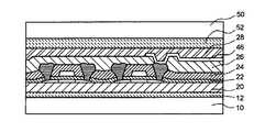
図4に、本願発明で提案する剥離方法を用いて、薄膜デバイスを転写するための当該薄膜デバイスの断面構造を示す。図4では、一例として、前記アクティブマトリクスのスイッチング用トランジスタ部の断面構造を示している。本実施例では、基板10の上に剥離層12を形成し、更にその上に下地層20を介して薄膜トランジスタを形成する。
【0034】
(1)基板上10上に、剥離層12及び下地層20を形成する工程
基板10は、後述する照射光60が透過し得る透光性を有するものであって、薄膜デバイスの製造プロセスに対する耐熱性、耐食性を備えるものであれば良い。具体的な材料としては、石英ガラス、ソーダガラス、コーニング7059、日本電気ガラスOA−2等の耐熱性ガラスが挙げられる。基板10の厚さに大きな制限はないが、0.5mm〜2.0mm程度であることが好ましい。
【0035】
剥離層12は、後述する照射光60の照射により、当該層内や界面において剥離を生じる、または剥離し易くなるものを使用する。剥離層12として特定の物質を使用した場合、当該剥離層に一定の強度の光を照射することにより、前記剥離層を構成する原子または分子の結合力が消失または減少し、アブレーション等を生じて剥離に至る。また、照射光の照射によって、あるいは照射された光を吸収して当該物質が発熱することによって、前記剥離層を構成する物質が相変態を起こす場合がある。それに伴う体積変化、界面形状の変化、含有物質の析出や偏析等は、前記剥離層とそれに隣接する層(例えば図4では、基板10または下地層20)との間の密着性及び/または結合力を変化させ、前記剥離層の界面における剥離が生じ易くなる。また、照射光の照射によって放出された気体により、剥離に至る場合もある。これには、前記剥離層に含有されていた成分が気体となって放出される場合と、前記剥離層を構成する物質が前記照射光を吸収して気体に変化し、その蒸気が放出される場合とがある。
【0036】
剥離層12の具体的な組成としては、例えば特開平10−206896に記載されているように、
(a)非晶質シリコン、
(b)酸化ケイ素もしくはケイ酸化合物、酸化チタンもしくはチタン酸化合物、酸化ジルコニウムもしくはジルコン酸化合物、酸化ランタンもしくはランタン酸化合物の各種酸化物セラミックス、または誘電体あるいは半導体、
(c)窒化ケイ素、窒化アルミ、窒化チタン等の窒化物セラミックス、
(d)有機高分子材料、
(e)金属
等が考えられる。また、剥離層として好適な厚さ、形成方法等についても、同じく特開平10−206896に記載されている。
【0037】
前記薄膜デバイスとしてTFTを製造する場合には、剥離層12として非晶質シリコンを使用するのが好ましい。なぜなら、非晶質シリコンはTFTの活性層であるポリシリコンを形成する際に用いられる材料であるため、剥離層からTFTへの不純物元素の移行(換言すれば、活性ポリシリコン層の汚染)、TFTのプロセス温度に対する剥離層の耐熱性等を改めて考慮する必要がないからである。
【0038】
非晶質シリコンは、照射光、特にレーザ光を吸収して発熱し、その熱によって相変態を生じる。特に、一定のエネルギー以上の光を照射すると、非晶質シリコンは溶融、再結晶して多結晶シリコン(p−Si)に変化する。このとき、相変態に伴う体積変化、界面形状の変化等を生じて剥離を促進する。また、非晶質シリコン中には、水素(H)が含有されていても良い。この場合、水素の含有量は、2at%程度以上であることが好ましく、2〜20at%であることがより好ましい。なぜなら、非晶質シリコンに水素が含有されていると、照射光の照射により当該水素が放出され、剥離層の内圧が発生して剥離を促進するからである。水素の含有量は、成膜条件(例えばCVD法を用いて当該非晶質シリコンを形成する場合には、ガス組成、ガス圧、ガス雰囲気、ガス流量、ガス温度、基板温度等)を適宜設定することによって調整する。また、水素を含有しない、または水素含有量の少ない非晶質シリコンに対して、イオン注入法、またはイオンドーピング法等を用いて、水素またはその他の気体元素を含有せしめることもできる。
【0039】
下地層20は、絶縁性があり、前記薄膜デバイスを物理的及び/または化学的に保護することができる材料で構成するのが好ましい。更に、前記薄膜デバイスとして、例えばTFTを製造する場合には、TFTの製造プロセスと同一のプロセスで形成可能な絶縁膜である酸化シリコン(SiO2)、窒化シリコン(SiN)等が好ましく用いられる。
【0040】
下地層20の厚さは、前述の保護機能が果たせる程度であれば良い。下地層20として例えばSiO2、SiN等を用いた場合、50nm〜2.0μmであるのが好ましく、100〜500nmであるのが更に好ましい。また、下地層20の形成方法としては、熱酸化法、CVD法、スパッタリング法、スピンコート法等、を用いることができる。
【0041】
なお、図示はしていないが、基板10と剥離層12の間に中間下地層を形成することは好ましい。中間下地層は、下地層20と同様、SiO2、SiN等で構成し、基板10からの不純物元素の混入を防ぐ等の目的で用いられる。
【0042】
(2)下地層20の上に、薄膜デバイスを形成する工程(図4)
この工程では、通常の半導体プロセスにより薄膜トランジスタ等の薄膜デバイスを形成する。ここで記載するプロセスの詳細については、例えば電気情報通信学会論文誌C−II Vol.J76−C−II pp.227−234に記載されている。
【0043】
下地層20の上にアモルファスシリコン層を形成し、当該アモルファスシリコン層の全面に上方からレーザ光を照射してレーザアニール処理を施す。これにより、当該アモルファスシリコン層は溶融・再結晶化してポリシリコン層となる。その後、当該ポリシリコン層を所望の形状にパターニングして、活性シリコン層30を形成する。
【0044】
続いて、活性シリコン層30を覆うゲート絶縁膜22を、例えばCVD法により形成する。ゲート絶縁膜の組成としては、SiO2、SiN等が好ましく用いられる。また、ゲート絶縁膜32は、活性シリコン層30を高温で酸化することにより得られる熱酸化膜であっても構わない。
【0045】
次に、ゲート絶縁膜22の上に、ポリシリコン膜または金属膜を形成し、これをパターニングすることによりゲート電極40を形成する。
【0046】
次に、P型トランジスタの活性層にマスクを施し、全面にリン(P)等をイオン注入またはイオンドーピングすることにより、N型トランジスタのソース領域34及びドレイン領域36を形成する。このとき、活性シリコン領域32の上にはゲート絶縁膜22を介してゲート電極40が形成されているため、活性シリコン領域32には前記リン等の添加元素は導入されず、活性シリコン領域32、ソース領域34、及びドレイン領域36を自己整合的に形成することができる。
【0047】
同様の手法を用いて、N型トランジスタの活性層にマスクを施し、全面にボロン(B)等をイオン注入またはイオンドーピングすることにより、P型トランジスタのソース領域、ドレイン領域及び活性シリコン領域を形成する。
【0048】
次に、SiO2、SiN等で構成される層間絶縁膜24を、例えばCVD法により形成し、ソース領域34及びドレイン領域36に到達するコンタクトホールを、当該層間絶縁膜24に設ける。
【0049】
続いて、アルミニウム等で構成された金属膜を、例えばスパッタリング法により形成し、その後、当該金属膜をパターニングすることにより、ソース電極41及びドレイン電極42を形成する。
【0050】
以上の工程により、N型トランジスタとP型トランジスタで構成されたCMOSトランジスタ回路が完成する。
【0051】
なお、駆動用トランジスタTr1の、ゲート電極40及びソース電極41に相当する電極は、画素スイッチング用トランジスタTr2では、特にゲート線43及びデータ線44とそれぞれ称する。
【0052】
続いて、第二層間絶縁膜26を、例えばCVD法により形成し、画素スイッチング用トランジスタTr2のドレイン電極上にコンタクトホールを設ける。
【0053】
次に、例えばインジウム錫酸化物(ITO)等の、透明導電性材料から成る薄膜を形成し、これをパターニングすることにより、画素電極46を形成する。画素電極46は、液晶分子の配向を制御する電界を当該液晶分子に与える役割を果たす。以上の工程により、液晶を駆動するためのアクティブマトリクスが完成する。
【0054】
本工程の最後に、薄膜デバイスの表面を平坦化するための、絶縁性の平坦化膜28を、例えばCVD法やスピンコート法等により形成し、アクティブマトリクス基板が完成する。
【0055】
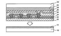
以上のような工程を経て、第1の基板上に剥離層を介して形成された薄膜デバイスを製造することができる。次に、当該薄膜デバイスを前記第1の基板から剥離して、第2の基板上に転写する工程1について説明する。
【0056】
(3)薄膜デバイス層に、仮接着層52を介して第2の基板50を貼り合わせる工程(図5)
仮接着層52としては、後に剥離が可能な、一時的接着剤となる接着剤を使用する。例えば、仮接着層52の材料として、反応性硬化型接着剤、熱硬化型接着剤、紫外線硬化型接着剤、嫌気硬化型接着剤、等の各種接着剤が挙げられる。具体的には、エポキシ系、アクリレート系、シリコーン系、等の接着剤が使用可能である。また、このような接着層は、例えばスピンコート法、塗布法、等により形成される。
【0057】
第2の基板50としては、一時的な転写基板として使用可能な程度の強度を備えていれば良い。第2の基板50を構成する材料としては、合成樹脂、ガラス材、セラミックス、金属、等が挙げられる。ガラス材としては、例えば低融点の安価なガラス材を用いても構わない。
【0058】
仮接着層52として光硬化型接着剤を使用する場合、第2の基板50としては、当該光硬化性接着剤を硬化させるための光を透過する性質を有するものが好ましく用いられる。この場合、前記アクティブマトリクス基板の最表面に当該光硬化型接着剤を塗布し、これに第2の基板50を貼り合わせた後、第2の基板50側から光を照射して光硬化型接着剤を硬化させる。
【0059】
仮接着層52として、前記光硬化型接着剤以外の接着剤を使用する場合には、第2の基板50として必ずしも光透過性を有するものを使用しなくても良い。この場合、前記アクティブマトリクス基板の最表面に当該接着剤を塗布し、これに第2の基板50を貼り合わせた後、当該接着剤の特性に応じた硬化方法により当該接着剤を硬化させる。
【0060】
(4)剥離層12に、第1の基板10側から照射光60を照射して当該剥離層12に剥離を生ぜしめ、第1の基板10を薄膜デバイス層から分離する工程(図6及び図7)
剥離を行うための照射光60としては、剥離層の層内及び/または界面において剥離を起こさせるものであれば、いかなるものでも良い。例えば、照射光60としては、X線、紫外線、可視光、赤外線(熱線)、レーザ光、ミリ波、マイクロ波、等の光を用いることができる。また、電子線、放射線(α線、β線、γ線)等であっても良い。このうち、剥離層12に剥離を生じさせ易いという点でレーザ光が好ましい。
【0061】
レーザ光を発生させるレーザ装置としては、各種気体レーザ、固体レーザ(半導体レーザ)、等が挙げられるが、特にエキシマレーザ、Nd−YAGレーザ、アルゴンレーザ、CO2レーザ、COレーザ、He−Neレーザ、等が好ましく、その中でも特にエキシマレーザが特に好ましい。エキシマレーザは、短波長域で高エネルギーを出力するため、極めて短時間で剥離層12に剥離を生じさせることができる。このため、隣接する層や近接する層にほとんど温度上昇を生じさせることなく、層の劣化や損傷を可能な限り少なくして剥離を行うことができる。
【0062】
レーザ光の波長は、100〜1200nmであるのが好ましく、100〜350nmであるのがより好ましい。特に、剥離層12を構成する材料として非晶質シリコン、またはシリコンを用いる場合、剥離層における短波長レーザ光の吸収効率が高いために、効果的な剥離を行うことができる。
【0063】
また、剥離層において、例えばガス放出、気化等の相変化を起こさせて剥離を行う場合には、波長が350〜1200nm程度のレーザ光を使用することもできる。
【0064】
レーザ光のエネルギー密度は、エキシマレーザの場合、10〜5000mJ/cm2程度とするのが好ましく、100〜1000mJ/cm2程度とするのがより好ましい。また、照射時間は、1〜1000nsec程度とするのが好ましく、10〜1000nsecとするのがより好ましい。エネルギー密度が低いか、または照射時間が短いと、剥離層12が剥離を起こすのに十分なエネルギーを当該剥離層に与えることができず、また、エネルギー密度が高いか、または照射時間が長いと、剥離層12及び/または下地層20を透過した光や剥離層12で過剰に生じた熱により、薄膜デバイスが損傷を受ける恐れがある。
【0065】
レーザ光の照射は、その強度が均一となるように照射するのが好ましい。光の照射方向は、図6に示すように剥離層12に対して垂直な方向に限らず、剥離層12に対して所定の角度傾斜した方向であっても良い。また、剥離層12の面積が照射光の1回の照射面積より大きい場合には、当該剥離層の全領域に対して複数回に分割して照射光を照射しても良い。更に、同一箇所に複数回照射したり、異なる種類、異なる波長(波長域)の光を同一領域または異なる領域に複数回照射しても良い。
【0066】
上記のような方法を用いて、剥離層12に照射光を照射すると、剥離層12の層内及び/または界面において剥離が生じ、あるいは生じ易くなる。したがって、第1の基板10と第2の基板50とを引き剥がすような力を加えると、密着力が失われ、あるいは低下している剥離層12の層内及び/または界面において、第1の基板10を薄膜デバイスから分離することができる。
【0067】
図7は、剥離の形態の一例として、剥離層12と下地層20の界面において剥離を生じた場合について示している。しかしながら、剥離層12の組成や照射光60の照射条件等によっては、剥離層12の層内、あるいは第1の基板10と剥離層12の界面において剥離が生じる場合もある。このような場合は、洗浄、研磨、エッチング、等の方法を用いて、下地層20に残存した剥離層を取り除く。
【0068】
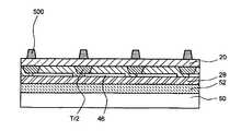
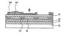
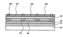
(5)第1の基板10を分離して露出した下地層20に、アクティブマトリクスの画素領域に対応させてカラーフィルタを形成する工程(図8乃至図12)
カラーフィルタを形成する工程は、下地層20に画素領域を区切るバンク500を形成する工程(図9)、バンク500で仕切られた画素領域内に、インクジェット方式によりカラーフィルタ形成用溶液501乃至503を充填する工程(図10及び図11)、充填されたカラーフィルタ形成用溶液を乾燥・定着させて着色層を形成する工程(図12)、で構成される。
【0069】
理解を容易にするため、図9乃至図12では画素スイッチング用トランジスタTr2と画素電極46を簡略化して示し、アクティブマトリクス領域に相当する部分断面図のみを表している。また、図8に示す断面図を上下反転し、下地層20が上を向くように示している。
【0070】
バンク500は、アクティブマトリクス基板の基板面に垂直な方向から見た場合、互いに隣接する画素領域の境界となるような形状(例えば格子形状やストライブ状)に、下地層20上に設けられる。バンク500の材料としては、例えば金属、SiO2等の無機材料や、レジストやポリイミド等の有機材料で構成することができる。また、光透過性のない材料でバンク500を形成することにより、バンク500にブラックマトリクスとしての機能を付加することができる。具体的には、ネガ型樹脂ブラック、高絶縁性ブラックマトリクス用レジストなど、黒色樹脂を有機溶剤に溶かしたものが使用可能である。ただし、アクティブマトリクスのゲート線及びデータ線をブラックマトリクスとして兼用する場合には、バンク500が必ずしも遮光性を有する必要はない。バンク500を所望の形状にパターニングするためには、例えばフォトリソグラフィ法を適用することができる。
【0071】
次に、バンク500によって区切られた画素領域に、インクジェット式記録ヘッドからフィルタ形成用溶液を充填させる。フィルタ形成用溶液は、染料や顔料を適当な溶剤に溶かして、インクジェット式記録ヘッドから吐出可能な粘度(数pc程度)に調整したものである。インクジェット式記録ヘッド510としては、溶液に熱による変性を生じさせないためピエゾジェット方式のものが好ましい。
【0072】
フィルタ形成用溶液は、原色(一般的には光の三原色である、赤、緑、青)の数だけ準備する。このフィルタ形成用溶液を充填したインクジェット式記録ヘッドから、該当する画素領域に打ち分け、バンク500内に適量充填する。充填する溶液量は、溶剤の揮発による体積減少を考慮した量に設定する。このとき、バンク500に対して、フィルタ形成用溶液との親和性を減少または失わせるような処理(例えば、フッ素化処理等)を行うことにより、隣接する画素への誤った溶液の溢れ、または漏れを防ぐことができる。
【0073】
画素領域にフィルタ形成用溶液を充填した後、熱処理等を行って溶媒を揮発させ、固化した着色層501乃至503を形成する。熱処理は、例えばヒータ、オーブン等を用いて行われ、全体を所定の温度に加熱して行われる。フィルタ形成用溶液の溶媒が揮発すると体積が減少するが、体積減少が著しい場合には、カラーフィルタとして機能するのに十分な着色層の厚みが得られるまで、溶液の充填と乾燥を繰り返す。着色層501乃至503が一定の厚みになったら、完全に乾燥させるため、所定の温度及び時間(例えば、120℃、1時間程度)の加熱を行う。
【0074】
(6)カラーフィルタ上に、接着層74を介して偏光機能を有する第3の基板70を貼り合わせる工程(図13乃至図14)
カラーフィルタを保護する目的で、カラーフィルタ上に保護層72を設けることは好ましい。これにより、接着剤によるカラーフィルタの溶解、汚染等を防ぐことができる。保護層72としては、SiO2、ポリシラザン、ポリイミド等の有機透明材料または無機透明材料を用いることができる。
【0075】
接着層74としては、反応硬化型接着剤、熱硬化型接着剤、紫外線硬化型接着剤等の光硬化型接着剤、嫌気硬化型接着剤等の各種硬化型接着剤が好適に用いられる。接着剤の組成としては、エポキシ系、アクリレート系、シリコーン系等、いかなるものでも良い。
【0076】
接着層74の形成には、公知の方法を適用可能である。例えば、スピンコート法、ディッピング法、スプレーコート法、ロールコート法、バーコート法等によって前記硬化型接着剤を所定の厚みに塗布する。
【0077】
第3の基板70としては、光透過性があり、偏光機能を有する材料が好適に用いられる。基板70としてプラスチックからなる偏光板をそのまま利用することは、光透過性、偏光機能、可曲性、軽量性、対衝撃性等の好適な条件をすべて満たすため、好ましい。基板70としては、偏光板以外にも、例えば、ガラス、石英など、通常の液晶パネル用基板に偏光板を貼り合わせたものも使用可能である。
【0078】
(7)第2の基板50を仮接着層52から分離する工程(図15)
第2の基板50の分離は、仮接着層52に化学的な処理を施して、当該仮接着層52の接着力を低下または消失させることにより行う。例えば、仮接着層52に市販の水溶性接着剤を使用した場合には、全体を水中に浸すことにより仮接着層52のみを溶解し、第2の基板50を分離することが可能である。
【0079】
以上、(1)乃至(7)までの工程を経て、カラーフィルタ及び偏光機能を有するアクティブマトリクス基板の製造が完了する。次に、公知の技術を用いて液晶配向膜の形成、液晶の封入を行い、液晶表示装置の製造を行う。
【0080】
(8)第2の基板50を分離することにより露出した平坦化膜28上に、配向膜82を形成する工程(図16)
理解を容易にするため、図16では、図8乃至図15において上下を反転した様子を示している。平坦化膜28の表面を適切な方法で洗浄した後、ポリイミド等の樹脂を当該表面に塗布し、乾燥させる。続いて、配向制御のためのラビング処理を施し、配向膜82を形成する。ラビング処理は、偏光機能を有する基板70の偏光方向に合わせて行う。
【0081】
(9)偏光機能及び共通透明電極を備えた対向基板を製造する工程(図17)
対向基板90としては、第3の基板70と同様、光透過性があり、偏光機能を有する材料が好適に用いられる。対向基板90としてプラスチックからなる偏光板をそのまま利用することは、光透過性、偏光機能、可曲性、軽量性、対衝撃性等の好適な条件をすべて満たすため、好ましい。対向基板90としては、偏光板以外にも、例えば、ガラス、石英など、通常の液晶パネル用基板に偏光板を貼り合わせたものも使用可能である。
【0082】
対向基板90に、透明共通電極92を形成する。共通透明電極92は、光透過性及び導電性を有する材料であれば良く、例えばITOが好ましく用いられる。透明共通電極92は、対向基板90上にITOをスパッタリング、または蒸着することにより形成可能である。
【0083】
続いて、透明共通電極92上に配向膜84を形成する。ポリイミド等の樹脂を透明共通電極92表面に塗布し、乾燥させる。続いて、配向制御のためのラビング処理を施し、配向膜92を形成する。ラビング処理は、偏光機能を有する対向基板92の偏光方向に合わせて行う。
【0084】
(10)アクティブマトリクス基板と対向電極との間に液晶を封入する工程(図18)
対向基板の外周縁にシール材(図示せず)を形成し、アクティブマトリクス基板と貼り合わせる。この際、対向基板とアクティブマトリクス基板との間には、前記シール材の厚さ分の空隙が保持される。次に、この空隙に液晶材料を封入し、液晶層86を形成する。
【0085】
以上、(1)乃至(10)の工程により、図2に示すような、部品点数が少なく、軽く、少々の衝撃にも耐え、可曲性を有する、等の優れた特性を備えた新規な液晶表示装置の製造が可能となる。
【0086】
<第2の実施形態>
本願発明の第2の実施形態は、レリーフ染色法によってカラーフィルタを形成するものである。
【0087】
図19乃至図23に、本実施形態の製造工程断面図を示す。
【0088】
フィルタ形成までの工程(図4乃至図8)は、第1の実施形態と同様である。ただし、本実施形態では必ずしもバンクの形成工程を必要とせず、ゲート線及びデータ線をブラックマトリクスとして兼用する。
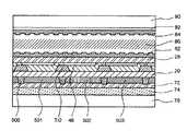
【0089】
本実施形態において、カラーフィルタを形成する工程は、下地層20上に、後に染色可能なレジスト600を塗布する工程(図19)、当該レジスト層600を画素領域に合わせて露光・現像する工程(図20乃至図21)、現像後に残されたレジスト層600を染色して着色層601乃至603を形成する工程(図21)、で構成される。
【0090】
下地層20上に、染料による染色が可能なレジストを利用してレジスト層600を形成する。例えば、レジストの材料として、セルロース、アクリル系樹脂、ゼラチン等、染料を吸収し得る性質を備えた材料を適用する。レジスト層600の塗布には、スピンコート法、スプレーコート法、ロールコート法、バーコート法、等を利用することができる。
【0091】
次に、塗布されたレジスト層600に対して、フォトマスク610を介して露光を行い、画素領域に対応したレジスト層を感光させる。この際、マスクするパターンは、同色の画素領域のみが露光されるようにする。レジスト層600がポジ型のレジストであれば、露光された部分のみが感光し、これを現像すると露光されたレジスト層が除去され、マスクされた部分のみが残される。図20乃至21では、レジスト層600としてポジ型のレジストを用いた場合について示している。レジスト層としてネガ型のレジストを用いた場合には、マスクデータの正反を逆転させたフォトマスクを用いる。
【0092】
続いて、画素領域ごとに残されたレジスト層600を、染料を使用して染色し、更に固着処理を行う。これにより、一色についての着色層601が形成される。
【0093】
一色の固着処理が終了したら、染料の色及び露光する画素領域を変えて、レジスト塗布(図19)、露光(図20)、現像(図21)、染色・固着(図22)を繰り返す。これらの処理を合計3回(それぞれ、赤、緑、青に対応)繰り返すことにより、各画素領域ごとに対応した着色層601乃至603が形成される(図22)。なお、一度固着処理が終了している着色層は、2回目及び/または3回目の染色工程による染色において、再度染色されることはないので、3色を個別に着色することができる。
【0094】
カラーフィルタ形成後の処理については、上記第1の実施形態と同様なので、省略する。
【0095】
<第3の実施形態>
本願発明の第3の実施形態は、感光性顔料分散法によってカラーフィルタを形成するものである。
【0096】
図24乃至図27に、本実施形態の製造工程断面図を示す。
【0097】
フィルタ形成までの工程(図4乃至図8)は、第1の実施形態と同様である。ただし、本実施形態では必ずしもバンクの形成工程を必要とせず、ゲート線及びデータ線をブラックマトリクスとして兼用する。
【0098】
本実施形態において、カラーフィルタを形成する工程は、下地層20上に、着色レジスト層700を塗布する工程(図24)、当該着色レジスト層700を画素領域に合わせて露光・現像する工程(図25乃至図26)、で構成される。
【0099】
下地層20上に、予め顔料が分散されている感光性レジストを塗布し、着色レジスト層700を形成する。
【0100】
次に、塗布された着色レジスト層700に対して、フォトマスク710を介して露光を行い、画素領域に対応した着色レジスト層を感光させる。この際、マスクするパターンは、同色の画素領域のみが露光されるようにする。着色レジスト層700がポジ型のレジストであれば、露光された部分のみが硬化し、これを現像すると露光された着色レジスト層が除去され、マスクされた部分の着色レジスト層のみが残される。図25乃至図26では、着色レジスト層700としてポジ型のレジストを用いた場合について示している。着色レジスト層としてネガ型のレジストを用いた場合には、マスクデータの正反を逆転させたフォトマスクを用いる。
【0101】
一色の現像処理が終了したら、着色レジスト層の色及び露光する画素領域を変えて、着色レジスト塗布(図24)、露光(図25)、現像(図26)、を繰り返す。これらの処理を合計3回(それぞれ、赤、緑、青に対応)繰り返すことにより、各画素領域ごとに対応した着色層701乃至703が形成される(図27)。
【0102】
カラーフィルタ形成後の処理については、上記第1の実施形態と同様なので、省略する。
【0103】
<第4の実施形態>
本願発明の第4の実施形態は、非感光性顔料分散法によってカラーフィルタを形成するものである。
【0104】
図28乃至図33に、本実施形態の製造工程断面図を示す。
【0105】
フィルタ形成までの工程(図4乃至図8)は、第1の実施形態と同様である。ただし、本実施形態では必ずしもバンクの形成工程を必要とせず、ゲート線及びデータ線をブラックマトリクスとして兼用する。
【0106】
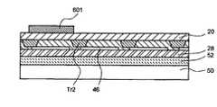
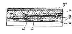
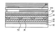
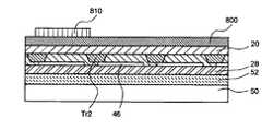
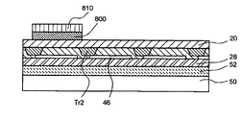
本実施形態において、カラーフィルタを形成する工程は、下地層20上に、非感光性の顔料分散樹脂層800を塗布する工程(図28)、レジスト層810を塗布する工程(図29)、当該着色レジスト層810を画素領域に合わせて露光・現像する工程(図30乃至図31)、非感光性の顔料分散樹脂層800をエッチングする工程(図32)、レジスト層810を剥離する工程(図33)、で構成される。
【0107】
下地層20上に、非感光性の顔料樹脂層800を塗布し、適切な方法で硬化させる。その上に、レジスト層810を形成し、フォトマスク820を介して露光を行い、画素領域に対応したレジスト層810を感光させる。この際、マスクするパターンは、同色の画素領域のみが露光されるようにする。レジスト層810がポジ型のレジストであれば、露光された部分のみが硬化し、これを現像すると露光されたレジスト層が除去され、マスクされた部分のレジスト層のみが残される。図30乃至図31では、レジスト層810としてポジ型のレジストを用いた場合について示している。レジスト層810としてネガ型のレジストを用いた場合には、マスクデータの正反を逆転させたフォトマスクを用いる。
【0108】
レジストの現像処理が終了したら、当該レジストをマスクとして、顔料樹脂層800をエッチングする。続けて、公知のレジスト除去剤を用いてレジストを剥離することにより、画素領域に対応した着色層801が形成される。
【0109】
一色のエッチング処理が終了したら、顔料樹脂層の色及び露光する画素領域を変えて、顔料樹脂層塗布(図28)、レジスト層形成(図29)、露光(図30)、現像(図31)、顔料樹脂層エッチング(図32)、レジスト層剥離(図33)を繰り返す。これらの処理を合計3回(それぞれ、赤、緑、青に対応)繰り返すことにより、各画素領域ごとに対応した着色層801乃至803が形成される(図34)。
【0110】
カラーフィルタ形成後の処理については、上記第1の実施形態と同様なので、省略する。
【0111】
<第5の実施形態>
本願発明の第5の実施形態は、印刷法によってカラーフィルタを形成するものである。
【0112】
図35に、本実施形態の製造工程断面図を示す。
【0113】
フィルタ形成までの工程(図4乃至図8)は、第1の実施形態と同様である。ただし、本実施形態では必ずしもバンクの形成工程を必要とせず、ゲート線及びデータ線をブラックマトリクスとして兼用する。
【0114】
本実施形態では、下地層20上に、オフセット印刷等の印刷法を適用して顔料樹脂を印刷する。印刷用ローラ900を用いて、画素領域のパターンに合わせて顔料樹脂を下地層20上に印刷する。図35では、例えば、赤色の顔料樹脂901、緑色の顔料樹脂902が既に印刷されている状態で、青色の顔料樹脂903を印刷している時の様子を示している。
【0115】
カラーフィルタ形成後の処理については、上記第1の実施形態と同様なので、省略する。
【0116】
<第6の実施形態>
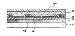
本願発明の第6の実施形態は、第1の基板10を薄膜デバイス層から分離することによって露出した下地層20の表面に、ブラックマトリクスを形成するものである。
【0117】
図36及び図37に、本実施形態の製造工程断面図を示す。
【0118】
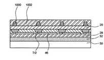
フィルタ形成までの工程(図4乃至図8)は、第一の実施形態と同様である。ブラックマトリクス1000を構成する材料としては、例えばアルミニウムやタンタル等の金属や、レジストやポリイミド等の有機材料等が挙げられる。ブラックマトリクス1000として前記有機材料を使用する場合には、遮光性を備えた材料を使用する。具体的には、ネガ型樹脂ブラック、高絶縁性ブラックマトリクス用レジストなど、黒色樹脂を有機溶剤に溶かしたものが使用可能である。
【0119】
ブラックマトリクス1000は、アクティブマトリクス基板の基板面に垂直な方向から見た場合、互いに隣接する画素領域の境界となるような形状(例えば格子形状やストライブ状)に、下地層20上に設けられる。ブラックマトリクス1000を所望の形状にパターニングするためには、例えばフォトリソグラフィ法を適用することができる。
【0120】
ブラックマトリクス形成後は、必要に応じて保護層1002を形成し、上記第1の実施形態と同様の方法を用いて、アクティブマトリクス及び/または駆動回路を偏光機能を有する第3の基板上へ転写する。
【0121】
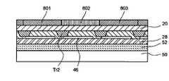
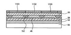
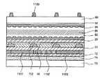
本実施形態では、アクティブマトリクス基板にカラーフィルタを内蔵していないので、カラーフィルタは対向基板90に設ける必要がある。この場合の製造工程断面図を、図37に示す。公知の技術を用いて、対向基板90にカラーフィルタ1011乃至1013、透明共通電極92、及び配向膜84を形成し、当該対向基板の外周縁にシール材(図示せず)を形成して、アクティブマトリクス基板と貼り合わせる。この際、アライメントマーク等を使用してアクティブマトリクス基板上の画素領域と、各画素に対応した対向基板上のカラーフィルタとが重なり合うように基板を貼り合わせる。対向基板とアクティブマトリクス基板との間には、前記シール材の厚さ分の空隙が保持され、この空隙に液晶材料を封入して、液晶層86を形成する。
【0122】
偏光板は、対向基板とは別の基板として用意する。
【0123】
なお、カラー表示を必要としない場合には、第1の実施形態と同様、偏光機能及び透明共通電極を備えた対向基板を使用することができる。
【0124】
<第7の実施形態>
本願発明の第7の実施形態は、第1の基板10を薄膜デバイス層から分離することによって露出した下地層20の表面にカラーフィルタを形成し、対向基板にブラックマトリクスを形成するものである。
【0125】
図38乃至図39に、本実施形態の製造工程断面図を示す。
【0126】
フィルタ形成までの工程(図4乃至図8)は、第1の実施形態と同様である。カラーフィルタは、第1乃至第5の実施形態のいずれかに記載の方法にて形成する。カラーフィルタ形成後は、上記第1の実施形態と同様の方法を用いて、アクティブマトリクス及び/または駆動回路を偏光機能を有する第3の基板上へ転写する。
【0127】
本実施形態では、アクティブマトリクス基板にブラックマトリクスを内蔵していないので、ブラックマトリクスは対向基板90に設ける必要がある。この場合の製造工程断面図を、図39に示す。公知の技術を用いて、対向基板にブラックマトリクス1100、透明共通電極92、及び配向膜84を形成する。偏光板としては、対向基板とは別の基板を用意する。
【0128】
ブラックマトリクス1100を備えた当該対向基板の外周縁にシール材(図示せず)を形成して、アクティブマトリクス基板と貼り合わせる。この際、アライメントマーク等を使用してアクティブマトリクス基板上の画素領域と、各画素に対応した対向基板上のブラックマトリクスとが重なり合うように基板を貼り合わせる。対向基板とアクティブマトリクス基板との間には、前記シール材の厚さ分の空隙が保持され、この空隙に液晶材料を封入して、液晶層86を形成する。
【0129】
なお、ブラックマトリクスをゲート線及びデータ線で代用する場合には、ブラックマトリクス1100は必ずしも必要ではないので、第1の実施形態と同様、偏光機能及び透明共通電極を備えた対向基板を使用することができる。
【0130】
【発明の効果】
本願発明によれば、最初に通常のTFT製造工程にて製造されたアクティブマトリクスを、第2の基板に転写し、露出した駆動層裏面にカラーフィルタ及び/またはブラックマトリクスを形成してから第3の基板に再度転写を行うので、通常は利用されない表面を利用したカラーフィルタ及び/またはブラックマトリクスの内蔵が可能となる。これにより、カラーフィルタ及び/またはブラックマトリクスを形成するために必要な基板枚数の削減が可能となり、デバイスの厚さを小さくすることができる。
【0131】
また、第3の基板として選択される材料は、アクティブマトリクスの製造工程に依存せず、任意の基板を選択することができる。従って、第3の基板として例えばプラスチックフィルム等を用いることにより、軽量で壊れ難く、可曲性を有する新規な液晶表示体を製造することが可能となる。
【0132】
更に本願発明では、マトリクス構造を有する表示領域に対して、位置を正確に合わせながらカラーフィルタ及び/またはブラックマトリクスを形成することができる。このため、位置合わせの困難性を低減して、カラーフィルタ及び/またはブラックマトリクスを容易に形成することが可能である。
【図面の簡単な説明】
【図1】従来の液晶表示装置の構成。
【図2】本願発明における液晶表示装置の構成。
【図3】本願発明における液晶表示装置の構成。
【図4】第1の実施形態の表示装置において、駆動用トランジスタ及び画素スイッチング用トランジスタの構造を説明する断面図。
【図5】第1の基板に第2の基板を仮接着する工程。
【図6】剥離層に照射光を照射し、剥離を生ぜしめる工程。
【図7】下地層と剥離層の界面において、第1の基板を分離する工程。
【図8】第1の基板を分離した後の断面構造を示す概略図。
【図9】下地層上に画素領域を区切るバンクを形成する工程。
【図10】バンクで区切られた画素領域内に、インクジェット方式によりカラーフィルタ形成用溶液を充填する工程。
【図11】カラーフィルタ形成用溶液がすべて充填された状態を示す断面図。
【図12】カラーフィルタ形成用溶液を乾燥・固化する工程。
【図13】カラーフィルタ上に保護層を形成する工程。
【図14】保護層上に第3の基板を接着する工程。
【図15】仮接着層から第2の基板を分離する工程。
【図16】平坦化膜上に配向膜を形成する工程。
【図17】対向基板に透明共通電極及び配向膜を形成する工程。
【図18】アクティブマトリクス基板と対向基板を、液晶を挟んで貼り合わせる工程。
【図19】第2の実施形態において、下地層にレジスト層を形成する工程。
【図20】レジスト層を露光する工程。
【図21】レジスト層を現像する工程。
【図22】レジスト層を着色し、カラーフィルタを形成する工程。
【図23】各画素領域にカラーフィルタを形成した状態を示す断面図。
【図24】第3の実施形態において、下地層に着色レジスト層を形成する工程。
【図25】着色レジスト層を露光する工程。
【図26】着色レジスト層を現像して、カラーフィルタを形成する工程。
【図27】各画素領域にカラーフィルタを形成した状態を示す断面図。
【図28】第4の実施形態において、下地層に顔料樹脂層を形成する工程。
【図29】顔料樹脂層上に、レジスト層を形成する工程。
【図30】レジスト層を露光する工程。
【図31】レジスト層を現像する工程。
【図32】顔料樹脂層をエッチングする工程。
【図33】レジスト層を剥離してカラーフィルタを形成する工程。
【図34】各画素領域にカラーフィルタを形成した状態を示す断面図。
【図35】第5の実施形態における印刷法の説明図。
【図36】第6の実施形態において、下地層にブラックマトリクス及び保護層を形成する工程。
【図37】第6の実施形態における液晶表示装置の構造を示す断面図。
【図38】第7の実施形態において、下地層にカラーフィルタを形成する工程。
【図39】第7の実施形態における液晶表示装置の構造を示す断面図。
【符号の説明】
100、200、300…バックライト
110、150、350…偏光板
120、220、320…アクティブマトリクス基板
122、222、322…アクティブマトリクス
124、224、324…駆動回路
126、226、326…実装テープ
130、230、330…液晶
140、240、340…対向基板
10、50、70、90…基板
12…剥離層
20…下地層
22、24、26、28、72、1002…絶縁層・保護層
30、32、34、36…半導体層
40、41、42、43、44…電極
46…透明画素電極
52、74…接着層
60…照射光
500、1000、1100…バンク
501、502、503、601、602、603、701、702、703、801、802、803、901、902、903、1011、1012、1013、1101、1102、1103…着色層
82、84…配向膜
92…透明共通電極
600、810…レジスト層
700、800…着色層
610、710、820…マスク
900…印刷用ローラ[0001]
BACKGROUND OF THE INVENTION
The present invention relates to a thin film device peeling method, an active matrix substrate manufactured by using the peeling method, and a liquid crystal display device using the active matrix substrate.
[0002]
[Prior art]
A liquid crystal display device using a thin film transistor (TFT) controls the optical rotatory power of liquid crystal molecules sealed between the substrate and a counter substrate by a voltage controlled by the thin film transistor formed on the substrate, and transmits light in each pixel. The principle of controlling light properties is used.
[0003]
A configuration example of such a liquid crystal display device is shown in FIG. The active matrix substrate 120 on which the active matrix 122 and / or the drive circuit 124 are formed and the counter substrate 140 are spaced apart from each other by a sealing material (not shown) formed along the outer peripheral edge of the counter substrate 140. The liquid crystal 130 is sealed in this gap.
[0004]
The pixel electrode formed in the active matrix 122 and the transparent counter electrode formed on the counter substrate 140 are opposed to each other with the liquid crystal 130 interposed therebetween, and liquid crystal molecules are driven by an electric field applied between the pixel electrode and the counter electrode. . An alignment film is formed on the surface of the active matrix 122 that is in contact with the liquid crystal 130 and the surface of the counter substrate 140 that is in contact with the liquid crystal 130, and determines the alignment of the liquid crystal molecules in an electric field-free state. The liquid crystal driving unit including the active matrix substrate 120, the liquid crystal 130, and the counter substrate 140 is further sandwiched between two polarizing plates 110 and 150 having different polarization directions. The polarization directions of the polarizing plates 110 and 150 are aligned with the alignment directions of the alignment films formed on the surfaces of the active matrix substrate 120 and the counter substrate 140, respectively.
[0005]
In order to enable color display, a color filter and / or a black matrix is formed on the counter substrate 140. Even when color display is not required, a black matrix for blocking transmitted light from between the pixel electrodes is required. The black matrix may be formed on the counter substrate 140, or may be substituted with a gate line and a data line constituting the active matrix.
[0006]
[Problems to be solved by the invention]
As described above, the liquid crystal display device has a structure in which a large number of substrates are bonded to each other, which increases the thickness of the display device. As the thickness of the liquid crystal display device increases, not only is it difficult to accurately align the position and angle of each substrate, but the projection light from the backlight cannot be effectively extracted. It is necessary to increase the luminance, which causes a disadvantage such as an increase in power consumption of the entire liquid crystal display device.
[0007]
Accordingly, the present invention provides a liquid crystal display device that can efficiently extract projection light by reducing the number of substrates necessary for manufacturing the liquid crystal display device and reducing the thickness of the device.
[0008]
[Means for Solving the Problems]
In order to solve the above problems, the present invention includes a step 1 of peeling a thin film device formed on a first substrate via a peeling layer from the first substrate and transferring the thin film device onto the second substrate;
And a step 2 of peeling the thin film device from the second substrate and transferring the thin film device onto the third substrate.
[0009]
The method of peeling the thin film device formed on the first substrate from the first substrate and transferring it onto an arbitrary substrate can be realized by a method disclosed in, for example, Japanese Patent Laid-Open No. 10-125931. Specifically, for example, a thin film device is formed on a first substrate having translucency through a release layer made of, for example, amorphous silicon, and then a laser is formed from the side opposite to the surface on which the thin film device is formed. Light is applied to the release layer. Thereby, peeling occurs in the peeling layer, and the thin film device is detached from the first substrate. At this time, after irradiating the release layer with the laser light, the thin film device on the first substrate is bonded to the second substrate through, for example, a water-soluble adhesive, and the first substrate and By applying a force that peels off the second substrate, Step 1 of transferring the thin film device onto the second substrate can be performed.
[0010]
[Means for Solving the Problems]
In order to solve the above problems, the present invention includes a step 1 of peeling a thin film device formed on a first substrate via a peeling layer from the first substrate and transferring the thin film device onto the second substrate; A method of manufacturing a liquid crystal display device using a matrix substrate manufactured by a method of peeling a thin film device, comprising: transferring the thin film device from the second substrate to a third substrate; A thin film transistor for switching pixels arranged in a matrix, a scanning line electrically connected to the gate of the transistor, a data line electrically connected to the source of the transistor, and a drain connected to the drain of the transistor The surface of the thin film device in contact with the release layer on the first substrate after the step 1, and a color filter and Or characterized by having a step of forming a black matrix.
The invention of the present application is the invention described above, wherein the thin film device includes a drive circuit that drives the thin film transistor for pixel switching.
The present invention is the invention described above, wherein the third substrate has a polarization function.
The present invention is the invention described above, wherein the third substrate has bendability.
The present invention is the invention described above, wherein the third substrate is a plastic substrate having a polarization function.
The invention of the present application is the invention as described above, wherein a counter substrate facing the active matrix substrate through a liquid crystal has a polarization function and includes a common transparent electrode.
The invention of the present application is the invention described above, wherein the counter substrate has bendability.
The invention of the present application is the invention described above, wherein the counter substrate has a polarization function and a common transparent electrode.
[0011]
As described above, after the steps 1 and 2, the thin film device has the same surface as that formed on the first substrate on the surface, and only the substrate is replaced with the third substrate. It becomes a state.
[0012]
As a medium for causing the thin film device manufactured by the above method to function as a liquid crystal display device, the invention described in claim 2 is an active matrix substrate manufactured using the thin film device peeling method defined in claim 1. The thin film device is
A thin film transistor for pixel switching arranged in a matrix, a scanning line electrically connected to the gate of the transistor, a data line electrically connected to the source of the transistor, and a drain connected to the drain of the transistor And an active matrix substrate.
[0013]
Further, as in the invention described in claim 3, it is more preferable that the thin film device is an active matrix substrate provided with a drive circuit for driving the pixel switching thin film transistor.
[0014]
A liquid crystal display device using these active matrix substrates has a higher contrast ratio than that of a simple matrix type, and is particularly suitable for color display. Furthermore, in the method in which the thin film device includes the drive circuit, it is not necessary to use an external circuit such as an LSI as the drive circuit. For this reason, there are no restrictions caused by connecting an external circuit to the active matrix substrate, and the selection range of a substrate material preferable as the third substrate can be widened. That is, it is possible to select a plastic as described later as the third substrate.
[0015]
The present invention is a liquid crystal display device manufactured using the active matrix substrate manufactured as described above, wherein the third substrate has a polarization function.
[0016]
A configuration example of such a liquid crystal display device is shown in FIG. The active matrix substrate 220 is obtained by transferring the thin film device including the active matrix 222 and / or the driving circuit 224 to the third substrate having a polarization function through the first and second steps. Thereby, the active matrix substrate 220 having both functions of the polarizing plate 110 and the active matrix substrate 120 shown in FIG. 1 can be manufactured.
[0017]
At this time, a novel liquid crystal display device having bendability can be realized by using a bendable substrate as the third substrate as in the fifth aspect of the present invention. More specifically, for example, a plastic substrate having a polarization function can be used as the third substrate as in the invention described in claim 6. In a conventional liquid crystal display device, quartz glass, heat-resistant glass, or the like has been used as a substrate for forming an active matrix. Since these materials are heavy and poor in impact resistance, as a matter of course, a liquid crystal display device using them has these properties. On the other hand, the plastic substrate is light, withstands slight impacts, and exhibits excellent characteristics such as bendability. When used, a new liquid crystal display device with these characteristics can be realized. can do.
[0018]
On the other hand, such a plastic substrate has a drawback that it has poor heat resistance as compared with a glass substrate, and this is the biggest cause that makes it difficult to form TFTs directly on the plastic substrate. However, a material having poor heat resistance can be used as the third substrate. The reason is as follows.
[0019]
Usually, the TFT manufacturing process is roughly divided into a high-temperature process that passes a process temperature of about 1100 ° C. and a low-temperature process that passes a process temperature of about 400 ° C. Needless to say, a substrate used for manufacturing such a TFT needs to have heat resistance enough to withstand these process temperatures. However, in the present invention, the third substrate is not used at the time of manufacturing the TFT, and is used only for the purpose of stably fixing the thin film device after the step 2. Accordingly, as the third substrate, heat resistance (for example, polyimide as the alignment film) that can withstand the formation temperature of the alignment film, the sealing material, etc., and the bonding temperature of the mounting tape for applying an electric signal to the active matrix substrate. If used, it is sufficient to have about 120 ° C.). Therefore, according to the present invention, it is possible to adopt a plastic substrate as the TFT substrate.
[0020]
The polarizing plate is composed of a polarizing element such as iodine or a dye, a polarizing substrate for aligning the polarizing element, and a protective substrate for the polarizing substrate. As materials used as these substrates, for example, plastic materials such as polyvinyl alcohol (PVA) as a polarizing substrate and triacetyl cellulose (TAC) as a protective substrate are used. In this invention, even if it is a polarizing plate manufactured using these plastic materials, it has the advantage that it can be used as it is as said 3rd board | substrate.
[0021]
The invention described in
[0022]
That is, in the state in which the thin film device is transferred onto the second substrate through the step 1, the thin film device is reversed and the back surface (the surface in contact with the first substrate) is exposed. It becomes. Therefore, a color filter and / or a black matrix can be formed on the back surface. The color filter can be formed using, for example, a coating method, a printing method, a photolithography method, an ink jet method, or a combination thereof.
[0023]
In addition, it is also possible to use a black matrix obtained by forming a metal thin film of aluminum, tantalum or the like by sputtering vapor deposition or the like and patterning it by photolithography.
[0024]
Note that a method of using the scanning lines and data lines of the active matrix as a black matrix is used as a known technique (for example, SID92DIGEST, pp.789-792). In this case as well, the color filter is activated. By incorporating in the matrix, it is not necessary to form a color filter on the counter substrate 140 shown in FIG.
[0025]
Further, as a configuration of a liquid crystal display device similar to the present invention, for example, a structure in which a color filter is disposed under a TFT (Japanese Patent Laid-Open No. 3-72322), and a structure in which a black matrix is disposed under a TFT (Japanese Patent Laid-Open No. 8-288519). ), Etc. are described. However, in the manufacturing process of the liquid crystal display device having these structures, a TFT manufacturing process requiring high temperature as described above must be performed using a substrate on which a color filter and / or a black matrix is formed. Accordingly, the material constituting the color filter and / or the black matrix must be specialized in a material having heat resistance equal to or higher than the TFT process temperature.
[0026]
On the other hand, in this invention, after manufacturing TFT by the method similar to the conventional process, a color filter and / or a black matrix are formed. In the subsequent process, as described above, since it is not exposed to a high temperature, it is not necessary to select a material having heat resistance as a material constituting the color filter and / or the black matrix. The width can be increased.
[0027]
The invention according to claim 11 is the liquid crystal display device characterized in that the counter substrate facing the active matrix through the liquid crystal has a polarization function and is provided with a common transparent electrode.
[0028]
By employing the counter substrate having such a function, the number of substrates constituting the liquid crystal display device can be reduced. That is, by providing a common transparent electrode on the surface of the polarizing plate 240 shown in FIG. 2 on the side in contact with the liquid crystal 230, the counter substrate 150 and the polarizing plate 160 shown in FIG. The counter substrate can be provided.
[0029]
As the counter substrate, a bendable substrate as in the invention described in
[0030]
As the counter substrate, specifically, a plastic substrate having a polarization function and having a common transparent electrode as in the inventions of
[0031]
If the active matrix substrate 220 shown in FIG. 2 does not necessarily include a color filter and / or a black matrix, these may be formed on the counter substrate as described in claims 15 and 16. Absent. A configuration example in this case is shown in FIG. In the liquid crystal display device having the configuration shown in FIG. 3, the functions of the counter substrate 340 and the polarizing plate 350 are the same as those of the counter substrate 140 and the polarizing plate 150 shown in FIG. However, even in this case, the number of the substrates constituting the liquid crystal display device can be reduced by providing the active matrix substrate 320 with a polarization function.
[0032]
DETAILED DESCRIPTION OF THE INVENTION
Next, embodiments of the present invention will be described with reference to the drawings.
[0033]
<First Embodiment>
FIG. 4 shows a cross-sectional structure of the thin film device for transferring the thin film device using the peeling method proposed in the present invention. FIG. 4 shows a cross-sectional structure of the switching transistor portion of the active matrix as an example. In this embodiment, a
[0034]
(1) Step of forming the
The board |
[0035]
As the
[0036]
As a specific composition of the
(A) amorphous silicon,
(B) silicon oxide or silicate compound, titanium oxide or titanate compound, zirconium oxide or zirconate compound, various oxide ceramics of lanthanum oxide or lanthanate compound, or dielectric or semiconductor,
(C) nitride ceramics such as silicon nitride, aluminum nitride, titanium nitride,
(D) an organic polymer material,
(E) Metal
Etc. are considered. Further, a suitable thickness, formation method and the like for the release layer are also described in JP-A-10-206896.
[0037]
When a TFT is manufactured as the thin film device, it is preferable to use amorphous silicon as the
[0038]
Amorphous silicon absorbs irradiation light, particularly laser light, and generates heat, and the heat causes phase transformation. In particular, when light of a certain energy or higher is irradiated, amorphous silicon is melted and recrystallized to change into polycrystalline silicon (p-Si). At this time, the volume change accompanying the phase transformation, the change in the interface shape and the like are caused to promote the peeling. Further, hydrogen (H) may be contained in the amorphous silicon. In this case, the hydrogen content is preferably about 2 at% or more, and more preferably 2 to 20 at%. This is because if amorphous silicon contains hydrogen, the hydrogen is released by irradiation with irradiation light, and an internal pressure of the peeling layer is generated to promote peeling. The hydrogen content is set appropriately according to the film formation conditions (for example, when the amorphous silicon is formed using the CVD method, the gas composition, gas pressure, gas atmosphere, gas flow rate, gas temperature, substrate temperature, etc.) To make adjustments. Alternatively, hydrogen or other gaseous elements can be contained in amorphous silicon that does not contain hydrogen or has a low hydrogen content by using an ion implantation method, an ion doping method, or the like.
[0039]
The
[0040]
The thickness of the
[0041]
Although not shown, it is preferable to form an intermediate underlayer between the
[0042]
(2) Step of forming a thin film device on the underlayer 20 (FIG. 4)
In this step, a thin film device such as a thin film transistor is formed by a normal semiconductor process. For details of the process described here, see, for example, IEICE Transactions C-II Vol. J76-C-II pp. 227-234.
[0043]
An amorphous silicon layer is formed on the
[0044]
Subsequently, a
[0045]
Next, a polysilicon film or a metal film is formed on the
[0046]
Next, a mask is applied to the active layer of the P-type transistor, and phosphorus (P) or the like is ion-implanted or ion-doped on the entire surface, thereby forming a
[0047]
Using the same method, the active layer of the N-type transistor is masked, and boron (B) or the like is ion-implanted or ion-doped on the entire surface to form the source region, drain region, and active silicon region of the P-type transistor. To do.
[0048]
Next, SiO2 The interlayer insulating
[0049]
Subsequently, a metal film made of aluminum or the like is formed by, for example, sputtering, and then the metal film is patterned to form the
[0050]
Through the above steps, a CMOS transistor circuit composed of an N-type transistor and a P-type transistor is completed.
[0051]
The electrodes corresponding to the
[0052]
Subsequently, the second
[0053]
Next, a
[0054]
At the end of this step, an insulating
[0055]
Through the steps as described above, a thin film device formed on the first substrate through a release layer can be manufactured. Next, step 1 of peeling the thin film device from the first substrate and transferring it to the second substrate will be described.
[0056]
(3) Step of bonding the
As the temporary
[0057]
The
[0058]
In the case where a photocurable adhesive is used as the temporary
[0059]
When an adhesive other than the photo-curing adhesive is used as the temporary
[0060]
(4) Step of separating the
As the
[0061]
Examples of laser devices that generate laser light include various gas lasers, solid-state lasers (semiconductor lasers), etc. Excimer lasers, Nd-YAG lasers, argon lasers, CO2 A laser, a CO laser, a He—Ne laser, and the like are preferable, and an excimer laser is particularly preferable among them. Since the excimer laser outputs high energy in a short wavelength region, the
[0062]
The wavelength of the laser light is preferably 100 to 1200 nm, and more preferably 100 to 350 nm. In particular, when amorphous silicon or silicon is used as a material for the
[0063]
In the peeling layer, for example, when peeling is performed by causing a phase change such as gas release or vaporization, a laser beam having a wavelength of about 350 to 1200 nm can be used.
[0064]
The energy density of the laser beam is 10 to 5000 mJ / cm in the case of an excimer laser.2 It is preferable to be about 100 to 1000 mJ / cm.2 More preferably, it is about. The irradiation time is preferably about 1 to 1000 nsec, more preferably 10 to 1000 nsec. When the energy density is low or the irradiation time is short, sufficient energy for the
[0065]
Laser light is preferably irradiated so that its intensity is uniform. As shown in FIG. 6, the light irradiation direction is not limited to the direction perpendicular to the
[0066]
When the
[0067]
FIG. 7 shows a case where peeling occurs at the interface between the peeling
[0068]
(5) A step of forming a color filter corresponding to the pixel region of the active matrix on the
The step of forming a color filter is a step of forming a
[0069]
For ease of understanding, FIGS. 9 to 12 show the pixel switching transistor Tr2 and the
[0070]
The
[0071]
Next, the pixel region delimited by the
[0072]
As many filter forming solutions as the number of primary colors (generally, the three primary colors of light, red, green and blue) are prepared. From the ink jet type recording head filled with the filter forming solution, it is divided into the corresponding pixel areas, and an appropriate amount is filled in the
[0073]
After the pixel region is filled with a filter forming solution, heat treatment or the like is performed to volatilize the solvent, and solidified
[0074]
(6) A step of attaching a
For the purpose of protecting the color filter, it is preferable to provide the
[0075]
As the
[0076]
A known method can be applied to the formation of the
[0077]
As the
[0078]
(7) Step of separating the
The separation of the
[0079]
As described above, through the steps (1) to (7), the manufacture of the active matrix substrate having the color filter and the polarization function is completed. Next, a liquid crystal display device is manufactured by forming a liquid crystal alignment film and encapsulating liquid crystals using a known technique.
[0080]
(8) Step of forming the
For ease of understanding, FIG. 16 shows a state in which the top and bottom are inverted in FIGS. After the surface of the
[0081]
(9) Process of manufacturing a counter substrate having a polarization function and a common transparent electrode (FIG. 17)
As the
[0082]
A transparent
[0083]
Subsequently, an
[0084]
(10) Step of sealing liquid crystal between the active matrix substrate and the counter electrode (FIG. 18)
A sealing material (not shown) is formed on the outer peripheral edge of the counter substrate, and is bonded to the active matrix substrate. At this time, a gap corresponding to the thickness of the sealing material is maintained between the counter substrate and the active matrix substrate. Next, a liquid crystal material is sealed in the gap to form a
[0085]
As described above, by the steps (1) to (10), as shown in FIG. 2, a novel component having excellent characteristics such as a small number of parts, light weight, withstands a little impact, and bendable. A liquid crystal display device can be manufactured.
[0086]
<Second Embodiment>
In the second embodiment of the present invention, a color filter is formed by a relief dyeing method.
[0087]
19 to 23 are sectional views of the manufacturing process of this embodiment.
[0088]
Processes up to filter formation (FIGS. 4 to 8) are the same as those in the first embodiment. However, in this embodiment, the bank formation process is not necessarily required, and the gate lines and the data lines are also used as a black matrix.
[0089]
In the present embodiment, the step of forming a color filter includes a step of applying a resist 600 that can be dyed on the underlying layer 20 (FIG. 19), and a step of exposing and developing the resist
[0090]
A resist
[0091]
Next, the applied resist
[0092]
Subsequently, the resist
[0093]
When the fixing process for one color is completed, the color of the dye and the pixel area to be exposed are changed, and resist coating (FIG. 19), exposure (FIG. 20), development (FIG. 21), and dyeing / fixing (FIG. 22) are repeated. By repeating these processes three times in total (corresponding to red, green and blue, respectively),
[0094]
Since the processing after forming the color filter is the same as that in the first embodiment, a description thereof will be omitted.
[0095]
<Third Embodiment>
In the third embodiment of the present invention, a color filter is formed by a photosensitive pigment dispersion method.
[0096]
24 to 27 are sectional views showing the manufacturing process according to this embodiment.
[0097]
Processes up to filter formation (FIGS. 4 to 8) are the same as those in the first embodiment. However, in this embodiment, the bank formation process is not necessarily required, and the gate lines and the data lines are also used as a black matrix.
[0098]
In the present embodiment, the step of forming a color filter includes a step of applying a colored resist
[0099]
A photosensitive resist in which a pigment is dispersed in advance is applied on the
[0100]
Next, the applied colored resist
[0101]
When the development processing for one color is completed, the color resist coating (FIG. 24), exposure (FIG. 25), and development (FIG. 26) are repeated while changing the color of the colored resist layer and the pixel area to be exposed. By repeating these processes three times in total (corresponding to red, green, and blue, respectively),
[0102]
Since the processing after forming the color filter is the same as that in the first embodiment, a description thereof will be omitted.
[0103]
<Fourth Embodiment>
In the fourth embodiment of the present invention, a color filter is formed by a non-photosensitive pigment dispersion method.
[0104]
FIG. 28 to FIG. 33 are sectional views of manufacturing steps of this embodiment.
[0105]
Processes up to filter formation (FIGS. 4 to 8) are the same as those in the first embodiment. However, in this embodiment, the bank formation process is not necessarily required, and the gate lines and the data lines are also used as a black matrix.
[0106]
In the present embodiment, the step of forming a color filter includes a step of applying a non-photosensitive pigment-dispersed
[0107]
A non-photosensitive
[0108]
When the resist development process is completed, the
[0109]
When the etching process for one color is completed, the color of the pigment resin layer and the pixel area to be exposed are changed to apply the pigment resin layer (FIG. 28), form the resist layer (FIG. 29), expose (FIG. 30), and develop (FIG. 31). The pigment resin layer etching (FIG. 32) and the resist layer peeling (FIG. 33) are repeated. By repeating these processes three times in total (corresponding to red, green, and blue, respectively),
[0110]
Since the processing after forming the color filter is the same as that in the first embodiment, a description thereof will be omitted.
[0111]
<Fifth Embodiment>
In the fifth embodiment of the present invention, a color filter is formed by a printing method.
[0112]
FIG. 35 shows a cross-sectional view of the manufacturing process of this embodiment.
[0113]
Processes up to filter formation (FIGS. 4 to 8) are the same as those in the first embodiment. However, in this embodiment, the bank formation process is not necessarily required, and the gate lines and the data lines are also used as a black matrix.
[0114]
In the present embodiment, a pigment resin is printed on the
[0115]
Since the processing after forming the color filter is the same as that in the first embodiment, a description thereof will be omitted.
[0116]
<Sixth Embodiment>
In the sixth embodiment of the present invention, a black matrix is formed on the surface of the
[0117]
FIG. 36 and FIG. 37 are cross-sectional views showing the manufacturing process of this embodiment.
[0118]
The steps up to filter formation (FIGS. 4 to 8) are the same as those in the first embodiment. Examples of the material constituting the
[0119]
The
[0120]
After the black matrix is formed, a
[0121]
In this embodiment, since the active matrix substrate does not include a color filter, it is necessary to provide the color filter on the
[0122]
The polarizing plate is prepared as a substrate different from the counter substrate.
[0123]
In the case where color display is not required, a counter substrate having a polarization function and a transparent common electrode can be used as in the first embodiment.
[0124]
<Seventh Embodiment>
In the seventh embodiment of the present invention, a color filter is formed on the surface of the
[0125]
38 to 39 show sectional views of the manufacturing process of this embodiment.
[0126]
Processes up to filter formation (FIGS. 4 to 8) are the same as those in the first embodiment. The color filter is formed by the method described in any one of the first to fifth embodiments. After the color filter is formed, the active matrix and / or the drive circuit is transferred onto the third substrate having a polarization function using the same method as in the first embodiment.
[0127]
In this embodiment, since the black matrix is not built in the active matrix substrate, it is necessary to provide the black matrix on the
[0128]
A sealing material (not shown) is formed on the outer peripheral edge of the counter substrate provided with the
[0129]
Note that when the black matrix is substituted with the gate line and the data line, the
[0130]
【The invention's effect】
According to the present invention, first, the active matrix manufactured in the normal TFT manufacturing process is transferred to the second substrate, and the color filter and / or the black matrix is formed on the exposed back surface of the driving layer. Since the transfer is performed again on this substrate, it is possible to incorporate a color filter and / or a black matrix using a surface that is not normally used. Thereby, it is possible to reduce the number of substrates necessary for forming the color filter and / or the black matrix, and the thickness of the device can be reduced.
[0131]
In addition, the material selected as the third substrate does not depend on the manufacturing process of the active matrix, and an arbitrary substrate can be selected. Therefore, by using, for example, a plastic film as the third substrate, it is possible to manufacture a novel liquid crystal display body that is lightweight, hardly broken, and has bendability.
[0132]
Furthermore, in the present invention, a color filter and / or a black matrix can be formed while accurately aligning the position of a display region having a matrix structure. For this reason, it is possible to easily form a color filter and / or a black matrix by reducing the difficulty of alignment.
[Brief description of the drawings]
FIG. 1 shows a configuration of a conventional liquid crystal display device.
FIG. 2 is a configuration of a liquid crystal display device according to the present invention.
FIG. 3 shows a configuration of a liquid crystal display device according to the present invention.
4 is a cross-sectional view illustrating the structure of a driving transistor and a pixel switching transistor in the display device of the first embodiment. FIG.
FIG. 5 is a step of temporarily bonding a second substrate to the first substrate.
FIG. 6 is a step of irradiating the peeling layer with irradiation light to cause peeling.
FIG. 7 shows a step of separating the first substrate at the interface between the base layer and the release layer.
FIG. 8 is a schematic diagram showing a cross-sectional structure after separating the first substrate.
FIG. 9 is a step of forming a bank for dividing a pixel region on a base layer.
FIG. 10 is a step of filling a color filter forming solution in a pixel region delimited by banks by an ink jet method.
FIG. 11 is a cross-sectional view showing a state in which all of the color filter forming solution is filled.
FIG. 12 is a process of drying and solidifying a color filter forming solution.
FIG. 13 shows a step of forming a protective layer on the color filter.
FIG. 14 shows a step of bonding a third substrate on the protective layer.
FIG. 15 shows a step of separating the second substrate from the temporary adhesive layer.
FIG. 16 shows a step of forming an alignment film on the planarizing film.
FIG. 17 shows a step of forming a transparent common electrode and an alignment film on the counter substrate.
FIG. 18 is a step of bonding an active matrix substrate and a counter substrate with liquid crystal sandwiched therebetween.
FIG. 19 is a step of forming a resist layer on the underlayer in the second embodiment.
FIG. 20 is a step of exposing a resist layer.
FIG. 21 is a step of developing a resist layer.
FIG. 22 is a step of coloring a resist layer to form a color filter.
FIG. 23 is a cross-sectional view showing a state in which a color filter is formed in each pixel region.
FIG. 24 is a step of forming a colored resist layer on the underlayer in the third embodiment.
FIG. 25 is a step of exposing a colored resist layer.
FIG. 26 is a step of developing a colored resist layer to form a color filter.
FIG. 27 is a cross-sectional view showing a state in which a color filter is formed in each pixel region.
FIG. 28 is a step of forming a pigment resin layer on the underlayer in the fourth embodiment.
FIG. 29 is a step of forming a resist layer on the pigment resin layer.
FIG. 30 shows a step of exposing a resist layer.
FIG. 31 is a step of developing a resist layer.
FIG. 32 is a step of etching the pigment resin layer.
FIG. 33 shows a step of peeling a resist layer to form a color filter.
FIG. 34 is a cross-sectional view showing a state in which a color filter is formed in each pixel region.
FIG. 35 is an explanatory diagram of a printing method according to the fifth embodiment.
FIG. 36 is a step of forming a black matrix and a protective layer in the base layer in the sixth embodiment.
FIG. 37 is a cross-sectional view showing a structure of a liquid crystal display device according to a sixth embodiment.
FIG. 38 shows a step of forming a color filter on the underlayer in the seventh embodiment.
FIG. 39 is a cross-sectional view showing the structure of a liquid crystal display device according to a seventh embodiment.
[Explanation of symbols]
100, 200, 300 ... Backlight
110, 150, 350 ... Polarizing plate
120, 220, 320 ... active matrix substrate
122, 222, 322 ... active matrix
124, 224, 324 ... drive circuit
126, 226, 326 ... Mounting tape
130, 230, 330 ... liquid crystal
140, 240, 340 ... counter substrate
10, 50, 70, 90 ... substrate
12 ... release layer
20 ... Underlayer
22, 24, 26, 28, 72, 1002 ... Insulating layer / protective layer
30, 32, 34, 36 ... semiconductor layer
40, 41, 42, 43, 44 ... electrode
46 ... Transparent pixel electrode
52, 74 ... Adhesive layer
60 ... Irradiation light
500, 1000, 1100 ... bank
501, 502, 503, 601, 602, 603, 701, 702, 703, 801, 802, 803, 901, 902, 903, 1011, 1012, 1013, 1101, 1102, 1103... Colored layer
82, 84 ... Alignment film
92 ... Transparent common electrode
600, 810 ... resist layer
700, 800 ... colored layer
610, 710, 820 ... mask
900 ... Printing roller
Claims (8)
Translated fromJapanese前記薄膜デバイスは、マトリクス状に配置された画素スイッチング用の薄膜トランジスタと、
当該トランジスタのゲートに電気的に接続された走査線と、
当該トランジスタのソースに電気的に接続されたデータ線と、
当該トランジスタのドレインに接続された画素電極と、
を備え、
前記工程1の後、前記薄膜デバイスの前記第1の基板上の前記剥離層に接していた面に、カラーフィルタ及び/またはブラックマトリックスを形成する工程を有することを特徴とする液晶表示装置の製造方法。A first step of peeling the thin film device formed on the first substrate through the peeling layer from the first substrate and transferring the thin film device onto the second substrate; A process for producing a liquid crystal display device using a matrix substrate produced by a thin film device peeling method comprising:
The thin film device is a thin film transistor for pixel switching arranged in a matrix,
A scan line electrically connected to the gate of the transistor;
A data line electrically connected to the source of the transistor;
A pixel electrode connected to the drain of the transistor;
With
After the step 1, there is a step of forming a color filter and / or a black matrix on the surface of the thin film device that is in contact with the release layer on the first substrate. Method.
前記第3の基板が偏光機能を有することを特徴とする液晶表示装置の製造方法。A manufacturing method of a liquid crystal display device according to claim 1 or 2,
A method for manufacturing a liquid crystal display device, wherein the third substrate has a polarization function.
Priority Applications (1)
| Application Number | Priority Date | Filing Date | Title |
|---|---|---|---|
| JP30277899AJP3911929B2 (en) | 1999-10-25 | 1999-10-25 | Manufacturing method of liquid crystal display device |
Applications Claiming Priority (1)
| Application Number | Priority Date | Filing Date | Title |
|---|---|---|---|
| JP30277899AJP3911929B2 (en) | 1999-10-25 | 1999-10-25 | Manufacturing method of liquid crystal display device |
Publications (3)
| Publication Number | Publication Date |
|---|---|
| JP2001125138A JP2001125138A (en) | 2001-05-11 |
| JP2001125138A5 JP2001125138A5 (en) | 2005-04-07 |
| JP3911929B2true JP3911929B2 (en) | 2007-05-09 |
Family
ID=17913016
Family Applications (1)
| Application Number | Title | Priority Date | Filing Date |
|---|---|---|---|
| JP30277899AExpired - Fee RelatedJP3911929B2 (en) | 1999-10-25 | 1999-10-25 | Manufacturing method of liquid crystal display device |
Country Status (1)
| Country | Link |
|---|---|
| JP (1) | JP3911929B2 (en) |
Families Citing this family (22)
| Publication number | Priority date | Publication date | Assignee | Title |
|---|---|---|---|---|
| TW564471B (en) | 2001-07-16 | 2003-12-01 | Semiconductor Energy Lab | Semiconductor device and peeling off method and method of manufacturing semiconductor device |
| TW554398B (en) | 2001-08-10 | 2003-09-21 | Semiconductor Energy Lab | Method of peeling off and method of manufacturing semiconductor device |
| TW558743B (en) | 2001-08-22 | 2003-10-21 | Semiconductor Energy Lab | Peeling method and method of manufacturing semiconductor device |
| US6953735B2 (en) | 2001-12-28 | 2005-10-11 | Semiconductor Energy Laboratory Co., Ltd. | Method for fabricating a semiconductor device by transferring a layer to a support with curvature |
| JP4186502B2 (en)* | 2002-04-22 | 2008-11-26 | ソニー株式会社 | Thin film device manufacturing method, thin film device, and display device |
| JP3965562B2 (en)* | 2002-04-22 | 2007-08-29 | セイコーエプソン株式会社 | Device manufacturing method, device, electro-optical device, and electronic apparatus |
| EP1363319B1 (en) | 2002-05-17 | 2009-01-07 | Semiconductor Energy Laboratory Co., Ltd. | Method of transferring an object and method of manufacturing a semiconductor device |
| US7183582B2 (en)* | 2002-05-29 | 2007-02-27 | Seiko Epson Coporation | Electro-optical device and method of manufacturing the same, element driving device and method of manufacturing the same, element substrate, and electronic apparatus |
| JP4373085B2 (en) | 2002-12-27 | 2009-11-25 | 株式会社半導体エネルギー研究所 | Semiconductor device manufacturing method, peeling method, and transfer method |
| KR101005569B1 (en) | 2002-12-27 | 2011-01-05 | 가부시키가이샤 한도오따이 에네루기 켄큐쇼 | Manufacturing Method of Semiconductor Device |
| WO2004064018A1 (en) | 2003-01-15 | 2004-07-29 | Semiconductor Energy Laboratory Co., Ltd. | Separating method and method for manufacturing display device using the separating method |
| JP4151420B2 (en) | 2003-01-23 | 2008-09-17 | セイコーエプソン株式会社 | Device manufacturing method |
| JP2004349513A (en) | 2003-05-22 | 2004-12-09 | Seiko Epson Corp | Thin film circuit device and method for manufacturing the same, electro-optical device, and electronic equipment |
| FR2870988B1 (en)* | 2004-06-01 | 2006-08-11 | Michel Bruel | METHOD FOR MAKING A MULTI-LAYER STRUCTURE COMPRISING, IN DEPTH, A SEPARATION LAYER |
| JP2004341557A (en)* | 2004-08-23 | 2004-12-02 | Semiconductor Energy Lab Co Ltd | Method for manufacturing semiconductor device |
| JP2006120726A (en) | 2004-10-19 | 2006-05-11 | Seiko Epson Corp | Thin film device manufacturing method, electro-optical device, and electronic apparatus |
| US7972910B2 (en) | 2005-06-03 | 2011-07-05 | Semiconductor Energy Laboratory Co., Ltd. | Manufacturing method of integrated circuit device including thin film transistor |
| US7820495B2 (en) | 2005-06-30 | 2010-10-26 | Semiconductor Energy Laboratory Co., Ltd. | Method for manufacturing semiconductor device |
| JP4610515B2 (en)* | 2006-04-21 | 2011-01-12 | 株式会社半導体エネルギー研究所 | Peeling method |
| JP4894415B2 (en)* | 2006-08-25 | 2012-03-14 | 凸版印刷株式会社 | Manufacturing method of liquid crystal display device |
| US7968388B2 (en) | 2007-08-31 | 2011-06-28 | Seiko Epson Corporation | Thin-film device, method for manufacturing thin-film device, and display |
| JP2016038490A (en)* | 2014-08-08 | 2016-03-22 | 株式会社半導体エネルギー研究所 | Display panel, display module, and electronic apparatus |
Family Cites Families (5)
| Publication number | Priority date | Publication date | Assignee | Title |
|---|---|---|---|---|
| JP2929704B2 (en)* | 1990-11-01 | 1999-08-03 | 松下電器産業株式会社 | Method of manufacturing liquid crystal display substrate |
| FR2679057B1 (en)* | 1991-07-11 | 1995-10-20 | Morin Francois | LIQUID CRYSTAL, ACTIVE MATRIX AND HIGH DEFINITION SCREEN STRUCTURE. |
| JPH09197405A (en)* | 1995-11-14 | 1997-07-31 | Sharp Corp | Viewing angle control type liquid crystal display device |
| JPH1126733A (en)* | 1997-07-03 | 1999-01-29 | Seiko Epson Corp | Transfer method of thin film device, thin film device, thin film integrated circuit device, active matrix substrate, liquid crystal display device, and electronic equipment |
| JPH11243209A (en)* | 1998-02-25 | 1999-09-07 | Seiko Epson Corp | Transfer method of thin film device, thin film device, thin film integrated circuit device, active matrix substrate, liquid crystal display device, and electronic equipment |
- 1999
- 1999-10-25JPJP30277899Apatent/JP3911929B2/ennot_activeExpired - Fee Related
Also Published As
| Publication number | Publication date |
|---|---|
| JP2001125138A (en) | 2001-05-11 |
Similar Documents
| Publication | Publication Date | Title |
|---|---|---|
| JP3911929B2 (en) | Manufacturing method of liquid crystal display device | |
| JP3738530B2 (en) | Color display device | |
| JP3738798B2 (en) | Method for manufacturing active matrix substrate and method for manufacturing liquid crystal panel | |
| JP5620921B2 (en) | Electronic device having plastic substrate and manufacturing method thereof | |
| KR101287478B1 (en) | Display device having oxide thin film transistor and method of fabricating thereof | |
| JP4363723B2 (en) | Liquid crystal display | |
| KR101258676B1 (en) | Liquid crystal display device and method for manufacturing the same | |
| KR100887671B1 (en) | Array substrate for liquid crystal display device and manufacturing method | |
| US6940578B2 (en) | Method for fabricating liquid crystal display device | |
| JP3809739B2 (en) | Manufacturing method of display device with filter | |
| JP5055849B2 (en) | Display device and organic thin film transistor manufacturing method | |
| KR100652052B1 (en) | Manufacturing Method of Array Substrate for Liquid Crystal Display | |
| JP2008009361A (en) | Liquid crystal display element and manufacturing method thereof | |
| JP3755573B2 (en) | Backlight built-in type liquid crystal display device and manufacturing method thereof | |
| JPH1068956A (en) | Liquid crystal display device and method of manufacturing the same | |
| JP3059049B2 (en) | Liquid crystal electro-optical device and method of manufacturing the same | |
| KR100774258B1 (en) | Inkjet Spacer for Liquid Crystal Display | |
| KR101753182B1 (en) | Method of fabricating array substrate using conductive ink | |
| KR101023292B1 (en) | Liquid Crystal Display Manufacturing Method | |
| JPH10333135A (en) | Liquid crystal display device | |
| JP4647434B2 (en) | Electrode substrate for liquid crystal display device, manufacturing method thereof, and liquid crystal display device | |
| JP3924992B2 (en) | Color filter and electro-optical device including the color filter | |
| KR101742125B1 (en) | Method of fabrication electrophoretic display deivce | |
| KR20070001505A (en) | Liquid crystal panel and its manufacturing method | |
| KR20070013722A (en) | Sealant and liquid crystal display including the same |
Legal Events
| Date | Code | Title | Description |
|---|---|---|---|
| A521 | Written amendment | Free format text:JAPANESE INTERMEDIATE CODE: A523 Effective date:20040527 | |
| A621 | Written request for application examination | Free format text:JAPANESE INTERMEDIATE CODE: A621 Effective date:20040527 | |
| A977 | Report on retrieval | Free format text:JAPANESE INTERMEDIATE CODE: A971007 Effective date:20060811 | |
| A131 | Notification of reasons for refusal | Free format text:JAPANESE INTERMEDIATE CODE: A131 Effective date:20060912 | |
| A521 | Written amendment | Free format text:JAPANESE INTERMEDIATE CODE: A523 Effective date:20061109 | |
| TRDD | Decision of grant or rejection written | ||
| A01 | Written decision to grant a patent or to grant a registration (utility model) | Free format text:JAPANESE INTERMEDIATE CODE: A01 Effective date:20070109 | |
| A61 | First payment of annual fees (during grant procedure) | Free format text:JAPANESE INTERMEDIATE CODE: A61 Effective date:20070122 | |
| R150 | Certificate of patent or registration of utility model | Free format text:JAPANESE INTERMEDIATE CODE: R150 | |
| FPAY | Renewal fee payment (event date is renewal date of database) | Free format text:PAYMENT UNTIL: 20110209 Year of fee payment:4 | |
| FPAY | Renewal fee payment (event date is renewal date of database) | Free format text:PAYMENT UNTIL: 20110209 Year of fee payment:4 | |
| FPAY | Renewal fee payment (event date is renewal date of database) | Free format text:PAYMENT UNTIL: 20120209 Year of fee payment:5 | |
| FPAY | Renewal fee payment (event date is renewal date of database) | Free format text:PAYMENT UNTIL: 20130209 Year of fee payment:6 | |
| FPAY | Renewal fee payment (event date is renewal date of database) | Free format text:PAYMENT UNTIL: 20130209 Year of fee payment:6 | |
| LAPS | Cancellation because of no payment of annual fees |