JP3908112B2 - Susceptor, epitaxial wafer manufacturing apparatus and epitaxial wafer manufacturing method - Google Patents
Susceptor, epitaxial wafer manufacturing apparatus and epitaxial wafer manufacturing methodDownload PDFInfo
- Publication number
- JP3908112B2 JP3908112B2JP2002220027AJP2002220027AJP3908112B2JP 3908112 B2JP3908112 B2JP 3908112B2JP 2002220027 AJP2002220027 AJP 2002220027AJP 2002220027 AJP2002220027 AJP 2002220027AJP 3908112 B2JP3908112 B2JP 3908112B2
- Authority
- JP
- Japan
- Prior art keywords
- susceptor
- wafer
- gas
- chamber
- Prior art date
- Legal status (The legal status is an assumption and is not a legal conclusion. Google has not performed a legal analysis and makes no representation as to the accuracy of the status listed.)
- Expired - Lifetime
Links
- 238000004519manufacturing processMethods0.000titleclaimsdescription35
- 239000007789gasSubstances0.000claimsdescription217
- 239000012159carrier gasSubstances0.000claimsdescription39
- 238000010438heat treatmentMethods0.000claimsdescription12
- 230000000149penetrating effectEffects0.000claimsdescription6
- 235000012431wafersNutrition0.000description190
- 239000002019doping agentSubstances0.000description23
- 230000002093peripheral effectEffects0.000description20
- 229910052710siliconInorganic materials0.000description16
- 239000010703siliconSubstances0.000description16
- XUIMIQQOPSSXEZ-UHFFFAOYSA-NSiliconChemical compound[Si]XUIMIQQOPSSXEZ-UHFFFAOYSA-N0.000description15
- HBMJWWWQQXIZIP-UHFFFAOYSA-Nsilicon carbideChemical compound[Si+]#[C-]HBMJWWWQQXIZIP-UHFFFAOYSA-N0.000description12
- 229910010271silicon carbideInorganic materials0.000description12
- 239000010408filmSubstances0.000description9
- 230000007246mechanismEffects0.000description9
- 230000002000scavenging effectEffects0.000description9
- XKRFYHLGVUSROY-UHFFFAOYSA-NArgonChemical compound[Ar]XKRFYHLGVUSROY-UHFFFAOYSA-N0.000description8
- 238000000034methodMethods0.000description7
- UFHFLCQGNIYNRP-UHFFFAOYSA-NHydrogenChemical compound[H][H]UFHFLCQGNIYNRP-UHFFFAOYSA-N0.000description6
- XYFCBTPGUUZFHI-UHFFFAOYSA-NPhosphineChemical compoundPXYFCBTPGUUZFHI-UHFFFAOYSA-N0.000description6
- 238000006243chemical reactionMethods0.000description6
- 230000008569processEffects0.000description5
- 239000010453quartzSubstances0.000description5
- VYPSYNLAJGMNEJ-UHFFFAOYSA-Nsilicon dioxideInorganic materialsO=[Si]=OVYPSYNLAJGMNEJ-UHFFFAOYSA-N0.000description5
- 238000012546transferMethods0.000description5
- 229910052786argonInorganic materials0.000description4
- 230000015572biosynthetic processEffects0.000description4
- SLLGVCUQYRMELA-UHFFFAOYSA-NchlorosiliconChemical compoundCl[Si]SLLGVCUQYRMELA-UHFFFAOYSA-N0.000description4
- MROCJMGDEKINLD-UHFFFAOYSA-NdichlorosilaneChemical compoundCl[SiH2]ClMROCJMGDEKINLD-UHFFFAOYSA-N0.000description4
- 238000000407epitaxyMethods0.000description4
- 238000012545processingMethods0.000description4
- ZDHXKXAHOVTTAH-UHFFFAOYSA-NtrichlorosilaneChemical compoundCl[SiH](Cl)ClZDHXKXAHOVTTAH-UHFFFAOYSA-N0.000description4
- 239000005052trichlorosilaneSubstances0.000description4
- OKTJSMMVPCPJKN-UHFFFAOYSA-NCarbonChemical compound[C]OKTJSMMVPCPJKN-UHFFFAOYSA-N0.000description3
- 239000005046ChlorosilaneSubstances0.000description3
- VEXZGXHMUGYJMC-UHFFFAOYSA-NHydrochloric acidChemical compoundClVEXZGXHMUGYJMC-UHFFFAOYSA-N0.000description3
- 229910052799carbonInorganic materials0.000description3
- KOPOQZFJUQMUML-UHFFFAOYSA-NchlorosilaneChemical compoundCl[SiH3]KOPOQZFJUQMUML-UHFFFAOYSA-N0.000description3
- 239000013078crystalSubstances0.000description3
- 238000009792diffusion processMethods0.000description3
- 239000000463materialSubstances0.000description3
- 229910000073phosphorus hydrideInorganic materials0.000description3
- 239000002994raw materialSubstances0.000description3
- 239000006227byproductSubstances0.000description2
- 230000008859changeEffects0.000description2
- 238000013461designMethods0.000description2
- 230000006866deteriorationEffects0.000description2
- 238000007599dischargingMethods0.000description2
- 230000000694effectsEffects0.000description2
- 238000011049fillingMethods0.000description2
- 229910052736halogenInorganic materials0.000description2
- 150000002367halogensChemical class0.000description2
- 150000002431hydrogenChemical class0.000description2
- 239000001257hydrogenSubstances0.000description2
- 229910052739hydrogenInorganic materials0.000description2
- 238000012423maintenanceMethods0.000description2
- 238000002791soakingMethods0.000description2
- 238000002230thermal chemical vapour depositionMethods0.000description2
- 239000011248coating agentSubstances0.000description1
- 238000000576coating methodMethods0.000description1
- 238000011109contaminationMethods0.000description1
- 238000000354decomposition reactionMethods0.000description1
- 230000007547defectEffects0.000description1
- 238000010586diagramMethods0.000description1
- 238000006073displacement reactionMethods0.000description1
- 230000003028elevating effectEffects0.000description1
- -1for exampleSubstances0.000description1
- 238000012986modificationMethods0.000description1
- 230000004048modificationEffects0.000description1
- 229910003465moissaniteInorganic materials0.000description1
- 238000007517polishing processMethods0.000description1
- 239000000047productSubstances0.000description1
- 238000000746purificationMethods0.000description1
- 230000000630rising effectEffects0.000description1
- 150000003376siliconChemical class0.000description1
- 239000000758substrateSubstances0.000description1
- 230000003746surface roughnessEffects0.000description1
- 239000010409thin filmSubstances0.000description1
Images


Classifications
- C—CHEMISTRY; METALLURGY
- C23—COATING METALLIC MATERIAL; COATING MATERIAL WITH METALLIC MATERIAL; CHEMICAL SURFACE TREATMENT; DIFFUSION TREATMENT OF METALLIC MATERIAL; COATING BY VACUUM EVAPORATION, BY SPUTTERING, BY ION IMPLANTATION OR BY CHEMICAL VAPOUR DEPOSITION, IN GENERAL; INHIBITING CORROSION OF METALLIC MATERIAL OR INCRUSTATION IN GENERAL
- C23C—COATING METALLIC MATERIAL; COATING MATERIAL WITH METALLIC MATERIAL; SURFACE TREATMENT OF METALLIC MATERIAL BY DIFFUSION INTO THE SURFACE, BY CHEMICAL CONVERSION OR SUBSTITUTION; COATING BY VACUUM EVAPORATION, BY SPUTTERING, BY ION IMPLANTATION OR BY CHEMICAL VAPOUR DEPOSITION, IN GENERAL
- C23C16/00—Chemical coating by decomposition of gaseous compounds, without leaving reaction products of surface material in the coating, i.e. chemical vapour deposition [CVD] processes
- C23C16/44—Chemical coating by decomposition of gaseous compounds, without leaving reaction products of surface material in the coating, i.e. chemical vapour deposition [CVD] processes characterised by the method of coating
- C23C16/455—Chemical coating by decomposition of gaseous compounds, without leaving reaction products of surface material in the coating, i.e. chemical vapour deposition [CVD] processes characterised by the method of coating characterised by the method used for introducing gases into reaction chamber or for modifying gas flows in reaction chamber
- C23C16/45519—Inert gas curtains
- C23C16/45521—Inert gas curtains the gas, other than thermal contact gas, being introduced the rear of the substrate to flow around its periphery
- C—CHEMISTRY; METALLURGY
- C23—COATING METALLIC MATERIAL; COATING MATERIAL WITH METALLIC MATERIAL; CHEMICAL SURFACE TREATMENT; DIFFUSION TREATMENT OF METALLIC MATERIAL; COATING BY VACUUM EVAPORATION, BY SPUTTERING, BY ION IMPLANTATION OR BY CHEMICAL VAPOUR DEPOSITION, IN GENERAL; INHIBITING CORROSION OF METALLIC MATERIAL OR INCRUSTATION IN GENERAL
- C23C—COATING METALLIC MATERIAL; COATING MATERIAL WITH METALLIC MATERIAL; SURFACE TREATMENT OF METALLIC MATERIAL BY DIFFUSION INTO THE SURFACE, BY CHEMICAL CONVERSION OR SUBSTITUTION; COATING BY VACUUM EVAPORATION, BY SPUTTERING, BY ION IMPLANTATION OR BY CHEMICAL VAPOUR DEPOSITION, IN GENERAL
- C23C16/00—Chemical coating by decomposition of gaseous compounds, without leaving reaction products of surface material in the coating, i.e. chemical vapour deposition [CVD] processes
- C23C16/44—Chemical coating by decomposition of gaseous compounds, without leaving reaction products of surface material in the coating, i.e. chemical vapour deposition [CVD] processes characterised by the method of coating
- C23C16/458—Chemical coating by decomposition of gaseous compounds, without leaving reaction products of surface material in the coating, i.e. chemical vapour deposition [CVD] processes characterised by the method of coating characterised by the method used for supporting substrates in the reaction chamber
- C23C16/4582—Rigid and flat substrates, e.g. plates or discs
- C23C16/4583—Rigid and flat substrates, e.g. plates or discs the substrate being supported substantially horizontally
- C23C16/4584—Rigid and flat substrates, e.g. plates or discs the substrate being supported substantially horizontally the substrate being rotated
- C—CHEMISTRY; METALLURGY
- C30—CRYSTAL GROWTH
- C30B—SINGLE-CRYSTAL GROWTH; UNIDIRECTIONAL SOLIDIFICATION OF EUTECTIC MATERIAL OR UNIDIRECTIONAL DEMIXING OF EUTECTOID MATERIAL; REFINING BY ZONE-MELTING OF MATERIAL; PRODUCTION OF A HOMOGENEOUS POLYCRYSTALLINE MATERIAL WITH DEFINED STRUCTURE; SINGLE CRYSTALS OR HOMOGENEOUS POLYCRYSTALLINE MATERIAL WITH DEFINED STRUCTURE; AFTER-TREATMENT OF SINGLE CRYSTALS OR A HOMOGENEOUS POLYCRYSTALLINE MATERIAL WITH DEFINED STRUCTURE; APPARATUS THEREFOR
- C30B25/00—Single-crystal growth by chemical reaction of reactive gases, e.g. chemical vapour-deposition growth
- C30B25/02—Epitaxial-layer growth
- C30B25/12—Substrate holders or susceptors
- C—CHEMISTRY; METALLURGY
- C30—CRYSTAL GROWTH
- C30B—SINGLE-CRYSTAL GROWTH; UNIDIRECTIONAL SOLIDIFICATION OF EUTECTIC MATERIAL OR UNIDIRECTIONAL DEMIXING OF EUTECTOID MATERIAL; REFINING BY ZONE-MELTING OF MATERIAL; PRODUCTION OF A HOMOGENEOUS POLYCRYSTALLINE MATERIAL WITH DEFINED STRUCTURE; SINGLE CRYSTALS OR HOMOGENEOUS POLYCRYSTALLINE MATERIAL WITH DEFINED STRUCTURE; AFTER-TREATMENT OF SINGLE CRYSTALS OR A HOMOGENEOUS POLYCRYSTALLINE MATERIAL WITH DEFINED STRUCTURE; APPARATUS THEREFOR
- C30B25/00—Single-crystal growth by chemical reaction of reactive gases, e.g. chemical vapour-deposition growth
- C30B25/02—Epitaxial-layer growth
- C30B25/14—Feed and outlet means for the gases; Modifying the flow of the reactive gases
- H—ELECTRICITY
- H01—ELECTRIC ELEMENTS
- H01L—SEMICONDUCTOR DEVICES NOT COVERED BY CLASS H10
- H01L21/00—Processes or apparatus adapted for the manufacture or treatment of semiconductor or solid state devices or of parts thereof
- H01L21/67—Apparatus specially adapted for handling semiconductor or electric solid state devices during manufacture or treatment thereof; Apparatus specially adapted for handling wafers during manufacture or treatment of semiconductor or electric solid state devices or components ; Apparatus not specifically provided for elsewhere
- H01L21/67005—Apparatus not specifically provided for elsewhere
- H01L21/67011—Apparatus for manufacture or treatment
- H01L21/67017—Apparatus for fluid treatment
- H—ELECTRICITY
- H01—ELECTRIC ELEMENTS
- H01L—SEMICONDUCTOR DEVICES NOT COVERED BY CLASS H10
- H01L21/00—Processes or apparatus adapted for the manufacture or treatment of semiconductor or solid state devices or of parts thereof
- H01L21/67—Apparatus specially adapted for handling semiconductor or electric solid state devices during manufacture or treatment thereof; Apparatus specially adapted for handling wafers during manufacture or treatment of semiconductor or electric solid state devices or components ; Apparatus not specifically provided for elsewhere
- H01L21/67005—Apparatus not specifically provided for elsewhere
- H01L21/67011—Apparatus for manufacture or treatment
- H01L21/67098—Apparatus for thermal treatment
- H01L21/67115—Apparatus for thermal treatment mainly by radiation
Landscapes
- Chemical & Material Sciences (AREA)
- Chemical Kinetics & Catalysis (AREA)
- General Chemical & Material Sciences (AREA)
- Engineering & Computer Science (AREA)
- Materials Engineering (AREA)
- Metallurgy (AREA)
- Organic Chemistry (AREA)
- Crystallography & Structural Chemistry (AREA)
- Mechanical Engineering (AREA)
- Chemical Vapour Deposition (AREA)
Description
Translated fromJapanese【0001】
【発明の属する技術分野】
本発明は、ウェーハにエピタキシャル層を形成するためのエピタキシャルウェーハ製造装置,サセプタ構造およびエピタキシャルウェーハ製造方法に関し、特に、エピタキシャルウェーハの表面周縁部におけるドーパント濃度の上昇を抑制可能なエピタキシャルウェーハ製造装置,サセプタ構造およびエピタキシャルウェーハ製造方法に関する。
【0002】
【従来の技術】
ウェーハの表面にシリコンの結晶層を成長させることにより、結晶欠陥がなく、所望の抵抗率を有するシリコンウェーハを製造する技術が知られている。このシリコンの結晶層は、例えば直径が200mmで厚さが0.75mmのウェーハの場合に数μm程度の厚さを有する極薄い層であり、一般的にエピタキシャル層と呼ばれ、このエピタキシャル層を形成する装置をエピタキシャルウェーハ製造装置と呼んでいる。エピタキシャルウェーハ製造装置は、膜厚制御の容易性および膜品質の面から、主にシリコンウェーハを1枚ずつ処理する枚葉式のものが使用されることが多くなった。
【0003】
図1に示すように、この枚葉式のエピタキシャルウェーハ製造装置においては、通常、ウェーハを1枚だけ水平に支持するサセプタ4(ウェーハ支持台)が処理チャンバ2内に設けられている。また、サセプタ4上にウェーハ12を搬送するために、ウェーハ12をサセプタ4に対して上下動させるためのリフト機構を設けている。リフト機構は、サセプタ4を貫通して延びる複数本のリフトピン23を有しており、これらのリフトピン23の上端にウェーハ12を載せ、サセプタ4に対して相対的にリフトピン23を上下動させることでウェーハ12を昇降させる。このようなリフト機構により、搬送用アームのハンドに載せられてチャンバ2内に運ばれてきたウェーハ12をサセプタ4上に移載したり、或いはその逆に、ウェーハ12をサセプタ4からハンドに受け渡したりすることが可能となる。
【0004】
また、エピタキシャル層の成長を行うためには、サセプタ4上で支持されたウェーハ12を高温に加熱する必要がある。このため、多数のハロゲンランプ(赤外線ランプ)等の熱源8,9を処理チャンバ2の上下に配置し、サセプタ4及びウェーハ12を加熱している。
【0005】
サセプタ4は、炭素Cの基材に炭化シリコンSiCの被膜を施したものであり、ウェーハ12を加熱する際にウェーハ12全体の温度を均一に保つ均熱盤としての役割を果たす。図2に示すようにサセプタ4の上面には、例えばシリコンウェーハを収めるためにウェーハ12より一回り大きく、深さがl〜2mm程度のウェーハポケットと呼ばれるくぼみが形成されている。ウェーハポケット13の内表面は、ウェーハの外周部のみで接触するようにテーパ面とする構成が用いられ、ウェーハポケット13の内表面とウェーハ12の面接触をできるだけ減らすように工夫が施されている。このウェーハポケット13内にウェーハ12を収容し、所定温度にて原料ガスを含むキャリアガス中にサセプタ4を保持することにより、ウェーハ12の表面にシリコン薄膜よりなるエピタキシャル層が成長する。ここで原料ガスとは、シリコンソースガスとドーパントガスを指している。
【0006】
シリコンソースガスには、トリクロロシランSiHCl3やジクロロシランSiH2Cl2等のクロロシラン系ガスが、またドーパントガスには、ジボラン(P型)やホスフィン(N型)が使われるのが一般的である。これらのガスはキャリアガスである水素H2とともにチャンバ内に導入され、ウェーハ表面において熱CVD反応によるシリコンエピタキシーとともに副生成物としてHClが生成する。従って、ウェーハ表面においてはシリコンエピタキシーが進行するが、ウェーハ裏面においては主にガス拡散による回り込みによりSi−H−Cl系雰囲気が形成され、Si−H−Cl系雰囲気でウェーハ裏面からのドーパント種の放出が起こる。
【0007】
その結果、ウェーハポケット13に充満したドーパント種を含む雰囲気が拡散によりウェーハ表面へ回り込み、ウェーハ12の表面周縁部において局所的に気相中のドーパント濃度が上昇するため、エピタキシャル層中のドーパント濃度がウェーハ表面周縁部において上昇する現象が見られる。
【0008】
上記のようにウェーハポケット13に充満したドーパント種を含む雰囲気がウェーハ表面に回り込むのを防ぐために、特開平10−223545号公報に記載された発明は、図16に示すようにウェーハポケット13の最外周部にサセプタ4の裏面に貫通する孔部50を設けている。このようにウェーハポケット13の最外周部にサセプタ4表面から裏面に貫通する孔部50を設けることにより、サセプタ4の表面側を流れる原料ガスを含むキャリアガスが孔部50を通ってサセプタ4の下方に流出するため、ウェーハポケット13に充満したドーパント種を含む雰囲気がウェーハ12の表面に回り込むのを防止することができる。
【0009】
【発明が解決しようとする課題】
特開平10−223545号公報に記載された発明のようにサセプタ4の表面側からサセプタ4の下方にガスを流出させる場合には、キャリアガスとともに反応性の強いトリクロロシランSiHCl3やジクロロシランSiH2Cl2等の原料ガスおよび気相中で分解したSiアモルファス、HClなどが下部チャンバ7bに大量に流出する。
【0010】
図1を参照すればわかる通り下部チャンバ7bは、ウェーハ12の回転駆動機構,リフト機構,搬送用アームの進入経路等を含んでおり、掃除をすることは非常に困難である。上記のような原料ガスや分解生成物の侵入は、大幅なメンテナンス時間の増大をもたらし、生産性の悪化要因となる。また、メンテナンス費用の増大も無視できない。
【0011】
さらに、下部チャンバ7b側からも熱源9により加熱しているため、チャンバ内壁の汚れはサセプタ4の加熱の不均一や再現性の悪化をもたらし、ウェーハ品質のバラツキの原因にもなる。
【0012】
本出願に係る発明は、上記のような問題点を解決するためになされたものであり、その目的とするところは、サセプタの表面側からサセプタの下方へ大量の原料ガスを流すことなく、ウェーハポケットに充満したドーパント種を含む雰囲気を排出可能なエピタキシャルウェーハ製造装置およびサセプタ構造を提供することにある。
【0013】
また、本出願に係る発明の他の目的は、サセプタの表面側からサセプタの下方へ原料ガスが流れにくいエピタキシャルウェーハ製造装置およびエピタキシャルウェーハ製造方法を提供することにある。
【0014】
【課題を解決するための手段】
上記目的を達成するため、本出願に係る第1の発明は、略円板形状をなし、表面にウェーハを収容する凹状のウェーハポケットを有するサセプタであって、前記サセプタの側面または裏面から前記ウェーハポケットに貫通するガス供給用路と、前記ウェーハポケットから前記サセプタの側面または裏面に貫通するガス排出用路と、を有するサセプタである。
【0015】
また、本出願に係る第2の発明は、前記ガス供給用路は、前記サセプタの回転にしたがって前記ウェーハポケット内にガスを供給する形状をなし、前記ガス排出用路は、前記サセプタの回転にしたがって前記ウェーハポケット内のガスを排出する形状をなす、ことを特徴とする上記第1の発明に記載のサセプタである。
【0016】
さらに、本出願に係る第3の発明は、ガスの供給口と排出口を有するチャンバと、前記チャンバ内に配置され、表面にウェーハを収容する凹状のウェーハポケットと、側面または裏面から前記ウェーハポケットに貫通するガス供給用路と、前記ウェーハポケットから側面または裏面に貫通するガス排出用路と、を有する略円板状のサセプタと、前記サセプタを支持する支持手段と、前記チャンバ内の前記サセプタとウェーハを加熱する加熱手段と、を備えるエピタキシャルウェーハ製造装置である。
【0017】
また、本出願に係る第4の発明は、前記チャンバ内の前記サセプタよりも上方にのみ原料ガスを含むキャリアガスを供給するガス供給口を備える、ことを特徴とする上記第3の発明に記載のエピタキシャルウェーハ製造装置である。
【0018】
さらに、本出願に係る第5の発明は、チャンバと、前記チャンバ内に配置され、表面にウェーハを収容する凹状のウェーハポケットを有するサセプタと、前記サセプタを支持する支持手段と、前記チャンバ内の前記サセプタとウェーハを加熱する加熱手段と、を備えるエピタキシャルウェーハ製造装置であって、前記チャンバ内の前記サセプタの上方に原料ガスを含むキャリアガスを供給するガス供給口と、前記チャンバ内の前記サセプタの下方に前記キャリアガスよりも重いガスを供給する重ガス供給口と、を備えるエピタキシャルウェーハ製造装置である。
【0019】
また、本出願に係る第6の発明は、チャンバ内に配置され、表面にウェーハを収容する凹状のウェーハポケットを有するサセプタの、前記ウェーハポケットにウェーハを載置するステップと、前記ウェーハポケットに前記サセプタの下部からガスを供給するステップと、前記ウェーハポケット内のガスを前記サセプタの下部から排出するステップと、前記チャンバ内の前記サセプタと前記ウェーハを加熱するステップと、を含むことを特徴とするエピタキシャルウェーハ製造方法である。
【0020】
さらに、本出願に係る第7の発明は、チャンバ内に配置されたサセプタ上にウェーハを載置するステップと、前記チャンバ内の前記サセプタの上方に原料ガスを含むキャリアガスを供給し、前記サセプタの下方に前記キャリアガスよりも重いガスを供給するステップと、前記チャンバ内の前記サセプタと前記ウェーハを加熱するステップと、を含むことを特徴とするエピタキシャルウェーハ製造方法である。
【0021】
【発明の実施の形態】
以下、本出願に係る発明の実施の形態について、図1〜図15および図17に基づいて詳細に説明する。
【0022】
[装置全体の説明]
図1は、本発明に係るエピタキシャルウェーハ製造装置1の概略構造を示す縦断面である。本発明のエピタキシャルウェーハ製造装置自体の概略構造は、従来技術で説明したエピタキシャルウェーハ製造装置とほぼ同様であるため、同一図面を用いて説明する。同図においては、チャンバ2の構造を主に記載しており、チャンバ2の下方に設けた回転駆動機構については、具体的な図示を省略している。
【0023】
チャンバ2は、円筒状のベースリング3を円板状の上部窓5および受皿状の下部窓6によって上下から挟んでなり、内部の閉空間は反応炉を形成する。上部窓5および下部窓6は、熱源からの光を遮ることが無いように透光性を有する石英を用いている。チャンバ2内に形成された反応炉は、ウェーハ12よりも上部の空間である上部チャンバ7aと、ウェーハ12よりも下部の空間である下部チャンバ7bとに大別される。
【0024】
さらに、反応炉を加熱する熱源8,9をチャンバ2の上下に備えている。本実施の形態においては、上下の熱源8,9はそれぞれ複数本のハロゲンランプ(赤外線ランプ)から構成されている。
【0025】
チャンバ2内には、ウェーハ12を上部に支持するサセプタ4を収納している。サセプタ4は上方から見ると円板形状をしており、その直径はウェーハ12よりも大きく、サセプタ4の上面にはウェーハ12が収納される円形凹状のウェーハポケット13を設けている。サセプタ4は、本例においては炭素Cの基材に炭化シリコンSiCの被膜を施したものであり、ウェーハ12を加熱する際にウェーハ12全体の温度を均一に保つ均熱盤としての役割を果たす。そのため、サセプタ4はウェーハ12よりも数倍の厚さおよび数倍の熱容量を有している。
【0026】
ウェーハ12の上面に均一なエピタキシャル層が形成されるように、エピタキシャル層成長処理操作の間、サセプタ4はウェーハ12の板面と平行な面内において垂直軸を回転中心として回転動をする。当然のことながら、サセプタ4に設けたウェーハポケット13の中心は、サセプタ4の回転中心と一致する。
【0027】
サセプタ4の下方には、サセプタ4の回転軸となる円柱状または円筒状のサセプタ支持軸14が垂直に配置され、サセプタ支持軸14の上部にはサセプタ4を水平に支持する3本のサセプタアーム15を備える。3本のサセプタアーム15は上方から見たときにそれぞれが120°の角度をなすように放射状に配置され、サセプタアーム15の先端に設けた上方向凸部がサセプタ4の下面に当接してサセプタ4を支持する。
【0028】
サセプタ支持軸14は、その軸心とサセプタ4の円板中心とが一致する位置に垂直に配置され、サセプタ支持軸14の回転によりサセプタ4が回転する。サセプタ支持軸14への回転は、不図示の回転駆動機構によって与えられる。サセプタ支持軸14およびサセプタアーム15は、下部熱源9からの光を遮ることのないよう、透光性の石英から形成されている。
【0029】
図2はサセプタ4の縦断面を模式的に表した図である。サセプタ4のウェーハポケット13は、以下に説明するように複数の段部およびテーパ面からなる。例えば、直径300mmのウェーハをエピタキシャル成膜処理する装置においては、サセプタ4として直径が350〜400mm、厚さが3〜6mmの円板部材を用いる。
【0030】
サセプタ4の上面外周から20〜40mm中心に向かった位置に、円形凹部である第1の段部30を設けている。第1の段部30はサセプタ4の上面から0.4〜0.7mm下がった位置に設けた円形の平坦面であり、サセプタ4の上面と平行すなわち水平面である。
【0031】
さらに、第1の段部30の外周から5〜6mm中心に向かった位置を始点として、緩やかな傾斜を有するテーパ面31を設けている。テーパ面31は、第1の段部30よりも更に約0.1mm程下がった位置から始まり、中心に向かって24〜27mmの距離に対して約0.1mm下がる勾配を有する非常に緩やかなロート形状をなす。
【0032】
テーパ面31から更に中心に向かって、円形凹部である第2の段部32を設けている。第2の段部32はテーパ面31から約0.3mm下がった位置に設けた円形の平坦面であり、サセプタ4の上面と平行すなわち水平面である。
【0033】
図2では説明の都合上2個しか図示していないが、第2の段部32には3個の貫通穴22が設けられ、各々の貫通穴22の上部は上方に向かって拡大開口する皿状穴22´を形成している。3個の貫通穴22にはそれぞれウェーハ支持用のリフトピン23が挿通している。この貫通穴22の穴径はリフトピン23の直径よりも大きくし、サセプタ4に対してリフトピン23が上下動する際に接触しない大きさを有するように形成する。
【0034】
リフトピン23は、石英,シリコンSi,炭化シリコンSiC,石英にシリコンSi又は炭化シリコンSiCの被膜を施したもの等よりなる。リフトピン23は円柱または円筒状をなし、上端部には、皿状穴22´に対応するように下部外周にテーパ面24bを有する頭部24を備える。この頭部24のテーパ面24bのテーパ角は、皿状穴22´のテーパ面のテーパ角と適合する。この結果、頭部24は皿状穴22´の内壁に対し優れたシールを与え、これにより原料ガスがリフトピン23と貫通穴22の内壁との間を通って漏れることが防止される。
【0035】
頭部24の上部24aは頂角が鈍角をなす円錐形状をなし、ウェーハ裏面を支持する際の接触面積を極めて小さくすることにより、リフトピン23によるウェーハ裏面への傷の発生を防止している。リフトピン23は頭部24がサセプタ4の皿状穴22´の内壁に係合し、リフトピン23が下降した状態においては、自重により鉛直に垂下される。このとき、頭部24の上部24aが第2の段部32の上面から突出することはない。
【0036】
図1に示すように、リフトピン23はサセプタ4に垂下され、その胴部はサセプタアーム15に設けた貫通穴を挿通している。リフトピン23は後述のリフトアーム16とは分離した独立の単体構造であるため、サセプタ4が回転するときには、サセプタ4とともにリフトピン23も回転するが、リフトアーム16は停止した状態を保つ。リフトピン23の胴部がサセプタアーム15に設けた貫通穴を挿通しているため、サセプタ4が回転したときに、リフトピン23が遠心力によって傾くのを防止することができる。
【0037】
サセプタ支持軸14の外周には、サセプタ支持軸14に対して摺動可能な内径を有する円筒状のリフト軸17を設けている。リフト軸17の上端には、上方から見た際にそれぞれが120°の角度をなすように放射状に配置された3本のリフトアーム16を備える。リフトピン23が下降してエピタキシャル成膜処理をしている間は、リフトアーム16とリフトピン23の下端は非接触状態を保ち、サセプタ4の回転時にリフトアーム16がリフトピン23に余計な負荷を加えることはない。
【0038】
ウェーハ12をサセプタ4から上昇させる場合には、各リフトピン23がリフトアーム16上に位置合わせされたところでサセプタ4の回転を停止させ、リフトアーム16を上昇またはサセプタ支持軸14を下降させる。それにより、リフトピン23の下端がリフトアーム16に当接してリフトピン23の頭部24がサセプタ4から上昇し、ウェーハ12は頭部24によって下方から押し上げられてウェーハポケット13から上昇する。
【0039】
図1に示すように、サセプタ4の外周にはサセプタ4を取り囲むように、サセプタ4とほぼ同じ厚さを有する円環状の余熱リング19を固定配置している。余熱リング19の内周面はサセプタ4の外周面に対して接触しないだけの間隔をとって配置され、サセプタ4は余熱リング19と独立して回転することができる。余熱リング19は、サセプタ4と同様に炭素Cの基材に炭化シリコンSiCの被膜を施したものであり、サセプタ4の外周部における熱容量の変化に伴う急激な温度変化を防止する役割を果たす。このようにサセプタ4の周りに余熱リング19を設けることにより、サセプタ4は中心部から外周部に亘ってほぼ均一に加熱される。
【0040】
図1に示すようにベースリング3には、ガス供給口10aとガス排出口11を設けている。同図向かって左側のガス供給口10aから原料ガスを含んだキャリアガスを供給し、右側のガス排出口11から排出する。チャンバ外部に設けた不図示のガス供給ユニットより、ガス供給口10aを通して、チャンバ2内に原料ガスおよびキャリアガスが供給される。
【0041】
ガス供給口10aは、ベースリング3の内周面において余熱リング19よりも上側に開口を有し、上部チャンバ7a内に水素ガスH2或いは、原料ガスを含んだ水素ガスを供給する。原料ガスは、主にトリクロロシランSiHCl3やジクロロシランSiH2Cl2等のクロロシラン系のシリコンソースガスに、ジボラン(P型)やホスフィン(N型)のドーパントガスが添加されたものである。これらのガスはキャリアガスである水素ガスH2とともに上部チャンバ7a内に導入される。
【0042】
さらに、下部供給口10bがガス供給口10aとは別に設けられ、チャンバ外部に設けた不図示のガス供給ユニットより、下部供給口10bを通して下部チャンバ7b内に水素ガスH2が供給される。下部供給口10bは、ベースリング3の内周面において余熱リング19よりも下側に開口を有し、下部チャンバ7b内に水素ガスH2を供給する。
このように、上部チャンバ7a側にのみ原料ガスを供給することにより、下部チャンバ7bにおける原料ガスの無用な反応を防止することができる。
【0043】
ガス排出口11は、ベースリング3の内周面に余熱リング19よりも上側および下側に2つの開口を有し、上部チャンバ7aおよび下部チャンバ7bからのガスをひとまとめにしてチャンバ2の外へ排出する。
【0044】
[第1の実施の形態]
次に第1の実施の形態におけるサセプタの構造について、図3〜図7を用いて詳細に説明する。
【0045】
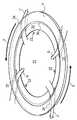
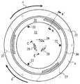
図3はサセプタ4の表面側の斜視図、図4はサセプタ4の裏面側の斜視図である。図3及び図4に示すようにサセプタ4は、サセプタ4の裏面側から厚さ方向でサセプタ4の中腹に至る4個の切欠きを備える。各切欠きは、サセプタ4の外周面に長方形の開口を有する。4個の切欠きは、サセプタ4の中心に対して対称の位置に配置された切欠き同士が対をなし、2個のガス流入用切欠き25と、2個のガス排出用切欠き26を形成する。図4に示すように、サセプタ4の裏面側から見ると、ガス流入用切欠き25とガス排出用切欠き26は緩やかな曲線を描く幅広の溝である。溝の断面形状は、サセプタ4の外周からサセプタ4の中心部に向かうにつれて狭くなる方が好ましいが、一定であってもよい。
【0046】
図5はサセプタ4の平面図、図6はサセプタ4の底面図である。図5に示すようにガス流入用切欠き25は右巻き方向で中心に向かって渦を巻くように形成され、ガス排出用切欠き26は右巻き方向で外側に向かって渦を巻くように形成される。
【0047】
図7は図5のB−B´断面図である。ガス流入用切欠き25とガス排出用切欠き26は共に同様な断面形状を有するため、ここではガス流入用切欠き25の断面形状についてのみ説明する。図7に示すように、ガス流入用切欠き25はサセプタ4の外周面からテーパ面31の開始位置に至るまで、中心方向に向かって溝を形成し、さらに、サセプタ4を斜めに10〜45°の角度で貫通してテーパ面31に開口を形成する。より好ましくはサセプタ4を20°の角度で貫通するのがよい。その結果、サセプタ4の裏面にはサセプタ4の外周面から中心方向に向かって曲線を描く溝が形成され、テーパ面31に差し掛かったところでウェーハポケット13に貫通する。
【0048】
図3の矢印aで示すように、上方から見た場合にサセプタ4は反時計方向に回転する。すると、矢印bで示すように下部チャンバ7b内のキャリアガスがサセプタ4のガス流入用切欠き25からウェーハポケット13内に流入し、矢印cで示すようにウェーハポケット13内のガスがガス排出用切欠き26から排出される。このように、サセプタ4の裏面側からガス流入用切欠き25を通ってキャリアガスが流入して、ウェーハポケット13内を循環し、ガス排出用切欠き26を通ってサセプタ4の裏面側に排出される。
【0049】
したがって、第1の実施の形態におけるサセプタ4によれば、サセプタ4の表面側からサセプタ4の下方へ大量の原料ガスを流すことなく、エピタキシャル成長の過程でウェーハの裏面から放散されるドーパント種を含む雰囲気をウェーハポケット13から排出することが可能になる。
【0050】
また、エピタキシャル成膜時におけるサセプタ4の回転を利用して、ウェーハポケット13内のガスを強制的に排出するため、ウェーハポケット13に充満したドーパント種を含む雰囲気がウェーハ12の表面に回り込むのをより効果的に防止することができる。本実施の形態においては、ガス流入用切欠き25とガス排出用切欠き26を曲線状の溝として形成することによりウェーハポケット13内のガスを強制的に排出する構成としたが、曲線状の溝でない場合であってもウェーハポケット13内のガスを排出する効果を奏することができる。
【0051】
更に、本実施の形態におけるサセプタ4によれば、ガス流入用切欠き25とガス排出用切欠き26が対称形状であるため、サセプタ4を正逆何れの方向に回転させた場合であっても、ウェーハポケット13内のガスを強制的に排出することができる。例えば、図5に示す反時計回りとは反対の方向(時計回り)に回転させた場合には、ガス流入用切欠き25がガス排出用として機能し、ガス排出用切欠き26がガス流入用として機能する。
【0052】
尚、本実施の形態においては、ガス流入用切欠き25およびガス排出用切欠き26は、サセプタ4の裏面側からテーパ面31に貫通している例を示したが、両方若しくは一方が第2の段部32に貫通していても良い。また、ガス流入用切欠き25およびガス排出用切欠き26の個数は設計により種々の変更が可能であり、それぞれが少なくとも1個以上であればよい。
【0053】
[第2の実施の形態]
図14及び図15に他の例を示す。図14はサセプタ4を上面から見た平面図、図15はD−D´断面図である。ウェーハの裏面形状は第1の実施の形態と同様であるため、図4を参照して説明する。
【0054】
サセプタ4は、第1の実施の形態と同様に、サセプタ4の裏面側から厚さ方向でサセプタ4の中腹に至る4個の切欠きを備え、各切欠きはサセプタ4の外周面に長方形の開口を有する。4個の切欠きは、サセプタ4の中心に対して対称の位置に配置された切欠き同士が対をなし、2個のガス流入用切欠き25と、2個のガス排出用切欠き26を形成する。図4に示すように、サセプタ4の裏面側から見ると、ガス流入用切欠き25とガス排出用切欠き26は緩やかな曲線を描く幅広の溝である。溝の断面形状は、サセプタ4の外周からサセプタ4の中心部に向かうにつれて狭くなる方が好ましいが、一定であってもよい。
【0055】
図14に示すようにガス流入用切欠き25は右巻き方向で中心に向かって渦を巻くように形成され、ガス排出用切欠き26は右巻き方向で外側に向かって渦を巻くように形成される。
【0056】
図15に示すように、本実施の形態におけるサセプタ4は、ウェーハ12を載置する面52と、その面52の外周部に形成された掃気段部51を備える。面52はサセプタ4の上面からおよそウェーハ12の形状に合わせて円形に凹んだ面である。掃気段部51は、面52よりも更にウェーハ裏面側に下がった段部であり、面52の外周に円環状に設けられた平坦面である。二点鎖線で示すウェーハ12は、掃気段部51よりも内側に形成された面52に載置され、外周部は掃気段部51の上を覆うように配置される。その結果、ウェーハ12と掃気段部51との間には、円環状空間53が形成される。なお、面52上には、メッシュ状の浅い細溝を形成する、いわゆるローレット加工を施していても良い。
【0057】
次に、本実施の形態におけるガス流入出用切欠き25及びガス排出用切欠き26の断面形状について説明する。ガス流入用切欠き25とガス排出用切欠き26は共に同様な断面形状を有するため、ここではガス流入出用切欠き25の断面形状についてのみ説明する。図15に示すように、ガス流入用切欠き25はサセプタ4の外周面から掃気段部51の開始位置に至るまで、中心方向に向かって溝を形成し、さらに、サセプタ4を斜めに10〜45°の角度で貫通して掃気段部51に開口を形成する。より好ましくはサセプタ4を20°の角度で貫通するのがよい。
【0058】
図14の矢印aで示すように、上方から見た場合にサセプタ4は反時計方向に回転する。すると、矢印bで示すようにサセプタ4の下部チャンバ7b内のキャリアガスがガス流入用切欠き25から掃気段部51に流入し、矢印cで示すようにガス排出用切欠き26から排出される。このように、サセプタ4の裏面側からガス流入用切欠き25を通ってキャリアガスが流入して、円環状空間53内を循環し、ガス排出用切欠き26を通ってサセプタ4の裏面側に排出される。
【0059】
したがって、第2の実施の形態におけるサセプタ4によれば、サセプタ4の表面側からサセプタ4の下方へ大量の原料ガスを流すことなく、ウェーハポケットに充満したドーパント種を含む雰囲気を排出することが可能になる。
【0060】
[第3の実施の形態]
次に第3の実施の形態におけるサセプタの構造について、図8〜図12を用いて詳細に説明する。
【0061】
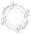
図8はサセプタ4の表面側の斜視図、図9はサセプタ4の裏面側の斜視図である。図8及び図9に示すようにサセプタ4は、サセプタ4の裏面側から厚さ方向でサセプタ4の中腹に至る3個の切欠きを備える。各切欠きは、サセプタ4の外周面に長方形の開口を有するガス流入用切欠き27である。図9に示すように、サセプタ4の裏面側から見ると、ガス流入用切欠き27は緩やかな曲線を描く幅広の溝である。溝の断面形状は、サセプタ4の外周からサセプタ4の中心部に向かうにつれて狭くなる方が好ましいが、一定であってもよい。
【0062】
図10はサセプタ4の平面図、図11はサセプタ4の底面図である。図10に示すように、サセプタ4は矢印aで示すように時計回りに回転するため、ガス流入用切欠き27は左巻き方向で中心に向かって渦を巻くように形成される。各ガス流入用切欠き27は、サセプタ4の中心に対して互いに120°の角度をなすように、等間隔に割り出しした位置に設けられている。
【0063】
図12(a)は図10のA−A´断面図である。図12(a)に示すように、ガス流入用切欠き27はサセプタ4の外周面からテーパ面31の開始位置に至るまで、中心方向に向かって溝を形成し、さらに、サセプタ4を斜めに10〜45°の角度で貫通してテーパ面31に開口を形成する。より好ましくはサセプタ4を20°の角度で貫通するのがよい。その結果、サセプタ4の裏面にはサセプタ4の外周面から中心方向に向かって曲線を描く溝が形成され、テーパ面31に差し掛かったところでウェーハポケット13に貫通する。
【0064】
図10に示すように、本実施の形態におけるサセプタ4は、サセプタ中央部近辺すなわち第2の段部32の平坦面に、サセプタ4を表面側から裏面側へ貫通するガス排出用開口28を設けている。図12(b)は、図10のC−C´断面図である。ガス排出用開口28は、ウェーハポケット13の第2の段部32の上面に開口を有し、サセプタ4を斜めに10〜45°の角度で貫通して、サセプタ4の裏面に再び開口を形成する。より好ましくはサセプタ4を20°の角度で貫通するのがよい。図10においては、ガス排出用開口28は断面形状を四角形に構成しているが、必ずしも四角形の必要はなく円形や三角形であってもよい。
【0065】
図8の矢印aで示すように、上方から見た場合にサセプタ4は時計方向に回転する。すると、矢印bで示すようにサセプタ4の下部チャンバ7b内のキャリアガスがガス流入用切欠き27からウェーハポケット13内に流入し、矢印cで示すようにウェーハポケット13内のガスがガス排出用開口28から排出される。このように、サセプタ4の裏面側からガス流入用切欠き27を通ってキャリアガスが流入して、ウェーハポケット13内を循環し、ガス排出用開口28を通ってサセプタ4の裏面側に排出される。
【0066】
したがって、第3の実施の形態におけるサセプタ4によれば、サセプタ4の表面側からサセプタ4の下方へ大量の原料ガスを流すことなく、ウェーハポケット13に充満したドーパント種を含む雰囲気を排出することが可能になる。
【0067】
また、エピタキシャル成膜時におけるサセプタ4の回転を利用して、ウェーハポケット13内のガスを強制的に排出するため、ウェーハポケット13に充満したドーパント種を含む雰囲気がウェーハ12の表面に回り込むのをより効果的に防止することができる。
【0068】
尚、本実施の形態においてガス流入用切欠き27は、サセプタ4の裏面側からテーパ面31に貫通している例を示したが、第2の段部32に貫通していても良い。また、ガス流入用切欠き27の個数は設計により種々の変更が可能であり、1個以上であればよい。
【0069】
第1〜第3の実施の形態に示したように、特に、ウェーハポケット13の形状は段部とテーパ面を組み合わせた構成である必要はなく、段部のみ或いはテーパ面のみ、またはいわゆるローレットというメッシュ状の浅い細溝が形成されてウェーハを多数の凸部と接触支持させる構成や、表面に被覆した炭化珪素の面粗度がウェーハ裏面よりもはるかに粗いことを利用する構成であってもよい。何れにしても本願発明は適用可能であり、サセプタ4の側面または裏面からウェーハポケット13内にガスを取り込み、再びサセプタ4の側面または裏面から排出する全ての構成に及ぶものである。
【0070】
[第4の実施の形態]
次に第4の実施の形態におけるサセプタの構造について、図17を用いて詳細に説明する。本実施の形態におけるサセプタの全体構成は、図8に示す第3の実施の形態におけるサセプタとほぼ同様であるため、同一部分については同一符号を付すことにより具体的な説明は省略する。
【0071】
図17はサセプタ4の表面側の斜視図である。本実施の形態におけるサセプタ4は、特に図17の太線で示すように、ガス逃がし溝20を備えた点に特徴を有する。ガス逃がし溝20は、テーパ面31に形成された円環状の浅い溝であり、各ガス流入用切欠き27のウェーハポケット13側の開口を連結するように形成されている。
【0072】
より詳細には、ガス逃がし溝20は溝幅3.0mm、溝深さ1.5mm程度で良く、もちろん、溝幅は3.0mm以上で溝深さが1.5mm以上であってもよい。排気効率を向上させる目的からは、溝幅は1.0mm以上で溝深さは0.5mm以上であることが望ましい。
【0073】
このように、各ガス流入用切欠き27のウェーハポケット13側の開口を連結する円環状のガス逃がし溝20を、テーパ面31に形成することにより、ガス逃がし溝20のある部分の排気効率を向上させ、或いは排気効率をウェーハの円周方向で均一化することができる。
【0074】
なお、本実施の形態におけるガス逃がし溝20を、上記第1の実施の形態におけるガス流入用切欠き25とガス排出用切欠き26のウェーハポケット側開口を連結する円環状に形成することも可能である。この場合においても、溝のある部分の排気効率を向上させ、或いは排気効率をウェーハの円周方向で均一化することができる。
【0075】
次に、本願発明のエピタキシャルウェーハ製造装置の全体の動作について、図1を用いて説明する。本動作説明においては、昇降機構や回転駆動機構の機械的な動作の説明は省略し、サセプタおよびリフトピンとウェーハとの動作関係、及び、それらの位置関係についてのみ説明する。
【0076】
まず、上下部の熱源8,9を作動させ、処理チャンバ2内のサセプタ4をウェーハの搬送に適した温度まで加熱する。ウェーハ搬送温度としては、800℃程度が好ましく、サーモセンサ等によってチャンバ2内のサセプタ4の温度を検知しながら上記の温度範囲を保つように制御する。同時に、ガス供給口10a及び下部供給口10bからキャリアガスを流し込み、上部チャンバ7a及び下部チャンバ7b内をキャリアガスによって充填する。チャンバ2はガス供給口10aの反対側にガス排出口11を有しており、ガス供給口10a及び下部供給口10bからガス排出口11に向かってキャリアガスが常時流れる。キャリアガスとしては一般に水素H2を用いることが多く、通常、常温(室温)の状態でチャンバ2内へ供給される。
【0077】
次に、チャンバ2内が十分に加熱されキャリアガスが充填されたら、今度はチャンバ2内にウェーハ12を搬入する。ウェーハ12はインゴットからスライス加工され、研磨工程等を経てなり、薄い円板状をなしている。一例としては、直径300mm,厚さ0.7〜0.75mm程度のものがある。このウェーハ12を石英製のハンドの上に載せ、ハンドをチャンバ2内に入れる。ウェーハ12を上昇したリフトピン23上に移載し、リフトピン23をゆっくりと下降させることによってウェーハ12がサセプタ4のウェーハポケット13に嵌り込み、左右方向の位置ずれが発生しない状態となる。
【0078】
上下部の熱源8,9を作動させ、ウェーハ表面温度をエピタキシャル成長に適した温度(1000〜1200℃)に上昇させる。また、不図示の制御部からの指令によって回転駆動用モータを駆動し、サセプタ4を回転させる。サセプタ4の回転が安定したら、キャリアガスに原料ガスを混合して、ガス供給口10aを通して上部チャンバ7a内に原料ガスを供給する。原料ガスは、主にトリクロロシランSiHCl3やジクロロシランSiH2Cl2等のクロロシラン系のシリコンソースガスに、ジボラン(P型)やホスフィン(N型)のドーパントガスが添加されたものである。
【0079】
ウェーハ12の表面を原料ガスを含むキャリアガスが流れ、ウェーハ表面にエピタキシャル層が成長し始める。ウェーハ12はサセプタ4に収容された状態で水平面内で回転しているため、ウェーハ12の表面にはほぼ均一な厚さを有するエピタキシャル層が成長する。このとき、ウェーハ表面において、熱CVD反応によるシリコンエピタキシーとともに副生成物としてHClが生成する。
【0080】
従来の装置によれば、ウェーハ表面においてはシリコンエピタキシーが進行するが、ウェーハ裏面においては主にガス拡散による回り込みによりウェーハポケット13内にSi−H−Cl系雰囲気が留まるため、Si−H−Cl系雰囲気でウェーハ裏面からのドーパント種の放出が起こる。
【0081】
上記の通り、第1〜第4の実施の形態において説明した本願のサセプタ4によれば、ウェーハ表面への成膜処理時の回転を利用して、サセプタ4の側面または裏面から下部チャンバ7b内のキャリアガス(原料ガスを含まない水素ガスH2)を吸気し、ウェーハポケット13内を循環させた後、サセプタ4の側面または裏面から排出する。その後、ガス排出口11の下側の開口からチャンバ外へ排出される。そのため、ウェーハポケット13内にSi−H−Cl系雰囲気が留まることを防止でき、ウェーハ裏面からのドーパント種の放出の影響を抑制することができる。
【0082】
所望の厚さのエピタキシャル層が成長したら、原料ガスの供給を停止し、熱源8,9を制御してチャンバ2内をウェーハ搬送温度に下げる。そして、処理済みのウェーハ12をチャンバ2内から搬出する。搬出は、搬入とは逆の手順に従えばよい。
【0083】
次に、本願におけるエピタキシャルウェーハ製造装置の変形例について説明する。図13は、エピタキシャルウェーハ製造装置40の概略構造を示す縦断面である。このエピタキシャルウェーハ製造装置40自体の概略構造は、図1を用いて説明したエピタキシャルウェーハ製造装置1とほぼ同様であるため、同様部分については同符号を付して詳細な説明は省略する。
【0084】
エピタキシャルウェーハ製造装置40は、ベースリング3に形成された重ガス供給口45に、重ガス供給手段41及びキャリアガス供給手段42を連結している。重ガス供給手段41には重ガス源44が流量調整手段43を介して接続されており、重ガス源44から供給される重ガスは流量調整手段43によって所望の供給量に調整される。重ガス供給手段41から供給される重ガスは、キャリアガス供給手段42から供給されるキャリアガスと混合され、重ガス供給口45から下部チャンバ7bへ供給される。ガス供給口10aから供給されるガスおよび重ガス供給口45から供給されるガスの供給量は、不図示のプロセスコントローラにより制御される。
【0085】
重ガス供給口45はガス供給口10aと交わることなく、チャンバ2外部から重ガスを下部チャンバ7bにのみ供給する。重ガスとしては、例えばアルゴンガスを用いることができる。基本的には、上部チャンバ7aに供給されるキャリアガスよりも重いことが必要である。重ガス源44としては、アルゴンガスタンクまたはアルゴンガス精製プラントからの配管を使用することができ、また、流量調整手段43としては、マスフローコントローラを使用することができる。
【0086】
重ガス供給口45から供給されたアルゴンガス等の重ガスは、チャンバ2の下部チャンバ7b内に充満する。重ガスは上部チャンバ7aに供給されるキャリアガスよりも重いため、下部チャンバ7b内を重ガスで満たすことにより、上部チャンバ7aからキャリアガスとともに原料ガスが流れ込むのを防止することができる。その結果、サセプタ4の表面側からサセプタ4の下方側へ大量の原料ガスを流すことなく、ウェーハポケットに充満したドーパント種を含む雰囲気を排出することができる。なお、図13においては、重ガス供給口45はキャリアガスと重ガスの混合ガスを供給する場合について例示しているが、キャリアガス供給口と重ガス供給口を独立して設けてもよい。
【0087】
【発明の効果】
本願のサセプタ構造によれば、サセプタの表面側からサセプタの下方へ大量の原料ガスを流すことなく、ウェーハポケットに充満したドーパント種を含む雰囲気を排出することが可能になる。
【0088】
また、本願のサセプタ構造によれば、エピタキシャル成膜時におけるサセプタの回転を利用してウェーハポケット内のガスを強制的に排出するため、ウェーハポケットに充満したドーパント種を含む雰囲気がウェーハの表面に回り込むのをより効果的に防止することができる。
【0089】
更に、ガス流入用切欠きとガス排出用切欠きを対称形状に形成することにより、サセプタを正逆何れの方向に回転させた場合であっても、ウェーハポケット内のガスを強制的に排出することができる。
【0090】
本願のエピタキシャルウェーハ製造装置によれば、上部チャンバに供給するキャリアガスよりも重いガスを下部チャンバに供給することにより、下部チャンバ内が重ガスで満たされ、上部チャンバからキャリアガスとともに原料ガスが流れ込むのを防止することができる。その結果、サセプタの表面側からサセプタの下方側へ大量の原料ガスを流すことなく、ウェーハポケットに充満したドーパント種を含む雰囲気を排出することができる。
【図面の簡単な説明】
【図1】本願のエピタキシャルウェーハ製造装置の概略を示す、縦断面図である。
【図2】サセプタの概略を示す、縦断面図である。
【図3】第1の実施の形態におけるサセプタの表面側の斜視図である。
【図4】第1の実施の形態におけるサセプタの裏面側の斜視図である。
【図5】第1の実施の形態におけるサセプタの平面図である。
【図6】第1の実施の形態におけるサセプタの底面図である。
【図7】図5に示すサセプタのB−B´断面図である。
【図8】第3の実施の形態におけるサセプタの表面側の斜視図である。
【図9】第3の実施の形態におけるサセプタの裏面側の斜視図である。
【図10】第3の実施の形態におけるサセプタの平面図である。
【図11】第3の実施の形態におけるサセプタの底面図である。
【図12】(a)は図10に示すサセプタのA−A´断面図、(b)は図10に示すサセプタのC−C´断面図である。
【図13】本願のエピタキシャルウェーハ製造装置の他の例を示す、縦断面図である。
【図14】第2の実施の形態におけるサセプタの平面図である。
【図15】図14に示すサセプタのD−D´断面図である。
【図16】従来技術のサセプタの概略を示す、縦断面図である。
【図17】第4の実施の形態におけるサセプタの表面側の斜視図である。
【符号の説明】
1…エピタキシャルウェーハ製造装置
2…チャンバ
3…ベースリング
4…サセプタ
5…上部窓
6…下部窓
7a…上部チャンバ 7b…下部チャンバ
8…熱源
9…熱源
10a…ガス供給口 10b…下部供給口
11…ガス排出口
12…ウェーハ
13…ウェーハポケット
14…サセプタ支持軸
15…サセプタアーム
16…リフトアーム
17…リフト軸
19…余熱リング
20…ガス逃がし溝
22…貫通穴 22´…皿状穴
23…リフトピン
24…頭部 24a…上部 24b…テーパ面
25…ガス流入用切欠き
26…ガス排出用切欠き
27…ガス流入用切欠き
28…ガス排出用開口
30…第1の段部
31…テーパ面
32…第2の段部
40…エピタキシャルウェーハ製造装置
41…重ガス供給手段
42…キャリアガス供給手段
43…流量調整手段
44…重ガス源
45…重ガス供給口
50…孔部
51…掃気段部
52…面
53…円環状空間。[0001]
BACKGROUND OF THE INVENTION
The present invention relates to an epitaxial wafer manufacturing apparatus, a susceptor structure, and an epitaxial wafer manufacturing method for forming an epitaxial layer on a wafer, and more particularly to an epitaxial wafer manufacturing apparatus and a susceptor capable of suppressing an increase in dopant concentration at the surface peripheral portion of the epitaxial wafer. The present invention relates to a structure and an epitaxial wafer manufacturing method.
[0002]
[Prior art]
A technique for manufacturing a silicon wafer having a desired resistivity without crystal defects by growing a silicon crystal layer on the surface of the wafer is known. This silicon crystal layer is an extremely thin layer having a thickness of about several μm in the case of a wafer having a diameter of 200 mm and a thickness of 0.75 mm, for example, and is generally called an epitaxial layer. The forming apparatus is called an epitaxial wafer manufacturing apparatus. As the epitaxial wafer manufacturing apparatus, a single-wafer type apparatus that mainly processes silicon wafers one by one has been frequently used from the viewpoint of easy film thickness control and film quality.
[0003]
As shown in FIG. 1, in this single wafer type epitaxial wafer manufacturing apparatus, a susceptor 4 (wafer support) for horizontally supporting only one wafer is usually provided in the processing chamber 2. In addition, a lift mechanism for moving the
[0004]
In order to grow an epitaxial layer, it is necessary to heat the
[0005]
The
[0006]
For the silicon source gas, trichlorosilane SiHCl3 And dichlorosilane SiH2 Cl2 In general, diborane (P-type) or phosphine (N-type) is used as the chlorosilane-based gas and the like as the dopant gas. These gases are hydrogen H, which is a carrier gas.2 At the same time, it is introduced into the chamber, and HCl is generated as a by-product along with silicon epitaxy by thermal CVD reaction on the wafer surface. Accordingly, although silicon epitaxy proceeds on the wafer surface, an Si—H—Cl based atmosphere is formed mainly by gas diffusion on the wafer back surface, and dopant species from the wafer back surface are formed in the Si—H—Cl based atmosphere. Release occurs.
[0007]
As a result, the atmosphere containing the dopant species filled in the
[0008]
In order to prevent the atmosphere containing the dopant species filled in the
[0009]
[Problems to be solved by the invention]
When the gas is allowed to flow out from the surface side of the
[0010]
As can be seen from FIG. 1, the
[0011]
Further, since heating is also performed from the
[0012]
The invention according to the present application has been made to solve the above-described problems, and the object of the invention is to flow a wafer without flowing a large amount of source gas from the surface side of the susceptor to the lower side of the susceptor. An object of the present invention is to provide an epitaxial wafer manufacturing apparatus and a susceptor structure capable of discharging an atmosphere containing dopant species filled in a pocket.
[0013]
Another object of the present invention is to provide an epitaxial wafer manufacturing apparatus and an epitaxial wafer manufacturing method in which the source gas hardly flows from the surface side of the susceptor to the lower side of the susceptor.
[0014]
[Means for Solving the Problems]
In order to achieve the above object, a first invention according to the present application is a susceptor having a substantially disk shape and having a concave wafer pocket for accommodating a wafer on a surface thereof, and the wafer from the side surface or the back surface of the susceptor. A susceptor having a gas supply path that penetrates into a pocket and a gas discharge path that penetrates from the wafer pocket to a side surface or a back surface of the susceptor.
[0015]
According to a second aspect of the present invention, the gas supply path is configured to supply gas into the wafer pocket according to the rotation of the susceptor, and the gas discharge path is configured to rotate the susceptor. Accordingly, the susceptor according to the first aspect of the present invention is characterized in that the gas in the wafer pocket is discharged.
[0016]
Furthermore, a third invention according to the present application includes a chamber having a gas supply port and a gas discharge port, a concave wafer pocket that is disposed in the chamber and accommodates a wafer on a front surface, and the wafer pocket from a side surface or a back surface. A substantially disk-shaped susceptor having a gas supply path penetrating through the wafer pocket and a gas discharge path penetrating from the wafer pocket to the side surface or the back surface; support means for supporting the susceptor; and the susceptor in the chamber And a heating means for heating the wafer.
[0017]
According to a fourth aspect of the present invention, there is provided a gas supply port for supplying a carrier gas containing a source gas only above the susceptor in the chamber. This is an epitaxial wafer manufacturing apparatus.
[0018]
Furthermore, a fifth invention according to the present application is directed to a chamber, a susceptor disposed in the chamber and having a concave wafer pocket on the surface for accommodating a wafer, support means for supporting the susceptor, An epitaxial wafer manufacturing apparatus comprising: a heating means for heating the susceptor and a wafer, wherein a gas supply port for supplying a carrier gas containing a source gas above the susceptor in the chamber; and the susceptor in the chamber An epitaxial wafer manufacturing apparatus comprising a heavy gas supply port for supplying a gas heavier than the carrier gas below the carrier gas.
[0019]
According to a sixth aspect of the present application, there is provided a step of placing a wafer in the wafer pocket of a susceptor that is disposed in the chamber and has a concave wafer pocket that accommodates the wafer on a surface thereof, Supplying a gas from a lower part of the susceptor; discharging a gas in the wafer pocket from a lower part of the susceptor; and heating the susceptor and the wafer in the chamber. It is an epitaxial wafer manufacturing method.
[0020]
Further, according to a seventh aspect of the present invention, there is provided a step of placing a wafer on a susceptor disposed in a chamber, supplying a carrier gas including a source gas above the susceptor in the chamber, and An epitaxial wafer manufacturing method comprising: supplying a gas heavier than the carrier gas below the substrate; and heating the susceptor and the wafer in the chamber.
[0021]
DETAILED DESCRIPTION OF THE INVENTION
Hereinafter, embodiments of the invention according to the present application will be described in detail with reference to FIGS. 1 to 15 and FIG. 17.
[0022]
[Description of the entire device]
FIG. 1 is a longitudinal section showing a schematic structure of an epitaxial
[0023]
The chamber 2 is formed by sandwiching a
[0024]
Furthermore,
[0025]
The chamber 2 houses a
[0026]
During the epitaxial layer growth processing operation, the
[0027]
Below the
[0028]
The
[0029]
FIG. 2 is a diagram schematically showing a longitudinal section of the
[0030]
A
[0031]
Furthermore, a
[0032]
A
[0033]
Although only two are illustrated in FIG. 2 for convenience of explanation, the
[0034]
The lift pins 23 are made of quartz, silicon Si, silicon carbide SiC, quartz having a silicon Si or silicon carbide SiC coating, or the like. The
[0035]
The
[0036]
As shown in FIG. 1, the
[0037]
A
[0038]
When the
[0039]
As shown in FIG. 1, an
[0040]
As shown in FIG. 1, the
[0041]
The
[0042]
Further, a
In this manner, by supplying the source gas only to the
[0043]
The
[0044]
[First Embodiment]
Next, the structure of the susceptor in the first embodiment will be described in detail with reference to FIGS.
[0045]
FIG. 3 is a perspective view of the front surface side of the
[0046]
FIG. 5 is a plan view of the
[0047]
7 is a cross-sectional view taken along the line BB ′ of FIG. Since both the
[0048]
As shown by an arrow a in FIG. 3, the
[0049]
Therefore, according to the
[0050]
In addition, since the gas in the
[0051]
Furthermore, according to the
[0052]
In the present embodiment, the
[0053]
[Second Embodiment]
14 and 15 show other examples. 14 is a plan view of the
[0054]
As in the first embodiment, the
[0055]
As shown in FIG. 14, the
[0056]
As shown in FIG. 15, the
[0057]
Next, cross-sectional shapes of the gas inflow /
[0058]
As shown by an arrow a in FIG. 14, the
[0059]
Therefore, according to the
[0060]
[Third Embodiment]
Next, the structure of the susceptor according to the third embodiment will be described in detail with reference to FIGS.
[0061]
8 is a perspective view of the front surface side of the
[0062]
FIG. 10 is a plan view of the
[0063]
FIG. 12A is a cross-sectional view taken along the line AA ′ of FIG. As shown in FIG. 12A, the
[0064]
As shown in FIG. 10, the
[0065]
As shown by the arrow a in FIG. 8, the
[0066]
Therefore, according to the
[0067]
In addition, since the gas in the
[0068]
In the present embodiment, the
[0069]
As shown in the first to third embodiments, in particular, the shape of the
[0070]
[Fourth Embodiment]
Next, the structure of the susceptor in the fourth embodiment will be described in detail with reference to FIG. Since the entire configuration of the susceptor in the present embodiment is substantially the same as that of the susceptor in the third embodiment shown in FIG. 8, the same parts are denoted by the same reference numerals, and detailed description thereof is omitted.
[0071]
FIG. 17 is a perspective view of the surface side of the
[0072]
More specifically, the
[0073]
In this way, by forming the annular
[0074]
The
[0075]
Next, the overall operation of the epitaxial wafer manufacturing apparatus of the present invention will be described with reference to FIG. In this description of the operation, description of the mechanical operation of the elevating mechanism and the rotation drive mechanism is omitted, and only the operation relationship between the susceptor and lift pins and the wafer and the positional relationship thereof will be described.
[0076]
First, the upper and
[0077]
Next, when the chamber 2 is sufficiently heated and filled with the carrier gas, the
[0078]
The upper and
[0079]
A carrier gas containing a source gas flows on the surface of the
[0080]
According to the conventional apparatus, silicon epitaxy proceeds on the wafer surface, but the Si—H—Cl-based atmosphere remains in the
[0081]
As described above, according to the
[0082]
When the epitaxial layer having a desired thickness is grown, the supply of the source gas is stopped, and the
[0083]
Next, a modification of the epitaxial wafer manufacturing apparatus in the present application will be described. FIG. 13 is a longitudinal section showing a schematic structure of the epitaxial
[0084]
In the epitaxial
[0085]
The heavy
[0086]
Heavy gas such as argon gas supplied from the heavy
[0087]
【The invention's effect】
According to the susceptor structure of the present application, it is possible to discharge the atmosphere containing the dopant species filled in the wafer pocket without flowing a large amount of source gas from the surface side of the susceptor to the lower side of the susceptor.
[0088]
In addition, according to the susceptor structure of the present application, the gas in the wafer pocket is forcibly discharged using the rotation of the susceptor during epitaxial film formation, so that the atmosphere containing the dopant species filled in the wafer pocket wraps around the surface of the wafer. Can be more effectively prevented.
[0089]
Further, by forming the gas inflow notch and the gas exhaust notch symmetrically, the gas in the wafer pocket is forcibly discharged even when the susceptor is rotated in either the forward or reverse direction. be able to.
[0090]
According to the epitaxial wafer manufacturing apparatus of the present application, by supplying a gas heavier than the carrier gas supplied to the upper chamber to the lower chamber, the lower chamber is filled with the heavy gas, and the source gas flows from the upper chamber together with the carrier gas. Can be prevented. As a result, the atmosphere containing the dopant species filled in the wafer pocket can be discharged without flowing a large amount of source gas from the surface side of the susceptor to the lower side of the susceptor.
[Brief description of the drawings]
FIG. 1 is a longitudinal sectional view schematically showing an epitaxial wafer manufacturing apparatus of the present application.
FIG. 2 is a longitudinal sectional view schematically showing a susceptor.
FIG. 3 is a perspective view of the surface side of the susceptor according to the first embodiment.
FIG. 4 is a perspective view of the back surface side of the susceptor in the first embodiment.
FIG. 5 is a plan view of a susceptor according to the first embodiment.
FIG. 6 is a bottom view of the susceptor in the first embodiment.
7 is a cross-sectional view taken along the line BB ′ of the susceptor shown in FIG.
FIG. 8 is a perspective view of the surface side of a susceptor according to a third embodiment.
FIG. 9 is a perspective view of a back surface side of a susceptor according to a third embodiment.
FIG. 10 is a plan view of a susceptor according to a third embodiment.
FIG. 11 is a bottom view of a susceptor according to a third embodiment.
12A is a cross-sectional view taken along line AA ′ of the susceptor shown in FIG. 10, and FIG. 12B is a cross-sectional view taken along line CC ′ of the susceptor shown in FIG.
FIG. 13 is a longitudinal sectional view showing another example of the epitaxial wafer manufacturing apparatus of the present application.
FIG. 14 is a plan view of a susceptor according to the second embodiment.
15 is a cross-sectional view taken along the line DD ′ of the susceptor shown in FIG.
FIG. 16 is a longitudinal sectional view showing an outline of a susceptor of the prior art.
FIG. 17 is a perspective view of the surface side of a susceptor according to a fourth embodiment.
[Explanation of symbols]
1. Epitaxial wafer manufacturing equipment
2 ... Chamber
3. Base ring
4 ... Susceptor
5 ... Upper window
6 ... Lower window
7a ...
8 ... Heat source
9 ... Heat source
10a ...
11 ... Gas outlet
12 ... wafer
13 ... Wafer pocket
14 ... Susceptor support shaft
15 ... Susceptor arm
16 ... Lift arm
17 ... Lift shaft
19 ... residual heat ring
20 ... Gas escape groove
22 ... through hole 22 '... dish hole
23 ... Lift pin
24 ...
25 ... Notch for gas inflow
26 ... Gas exhaust notch
27 ... Notch for gas inflow
28 ... Gas exhaust opening
30: First step
31 ... Taper surface
32 ... Second step
40. Epitaxial wafer manufacturing equipment
41. Heavy gas supply means
42. Carrier gas supply means
43 ... Flow rate adjusting means
44 ... Heavy gas source
45 ... Heavy gas supply port
50 ... hole
51. Scavenging step
52 ... surface
53 ... An annular space.
Claims (5)
Translated fromJapanese前記サセプタの側面または裏面から前記ウェーハポケットに貫通するガス供給用路と、
前記ウェーハポケットから前記サセプタの側面または裏面に貫通するガス排出用路と、
を有するサセプタ。A susceptor having a substantially disk shape and having a concave wafer pocket for accommodating a wafer on the surface,
A gas supply path that penetrates the wafer pocket from the side or back surface of the susceptor;
A gas exhaust passage penetrating from the wafer pocket to the side surface or the back surface of the susceptor;
Having a susceptor.
前記ガス排出用路は、前記サセプタの回転にしたがって前記ウェーハポケット内のガスを排出する形状をなす、
ことを特徴とする請求項1に記載のサセプタ。The gas supply path has a shape for supplying gas into the wafer pocket according to the rotation of the susceptor,
The gas discharge path is configured to discharge the gas in the wafer pocket according to the rotation of the susceptor.
The susceptor according to claim 1.
前記チャンバ内に配置され、表面にウェーハを収容する凹状のウェーハポケットと、側面または裏面から前記ウェーハポケットに貫通するガス供給用路と、前記ウェーハポケットから側面または裏面に貫通するガス排出用路と、を有する略円板状のサセプタと、
前記サセプタを支持する支持手段と、
前記チャンバ内の前記サセプタとウェーハを加熱する加熱手段と、
を備えるエピタキシャルウェーハ製造装置。A chamber having a gas supply port and a gas discharge port;
A concave wafer pocket which is disposed in the chamber and accommodates a wafer on the front surface; a gas supply passage which penetrates the wafer pocket from the side surface or the back surface; and a gas exhaust passage which penetrates from the wafer pocket to the side surface or the back surface; A substantially disc-shaped susceptor having
Support means for supporting the susceptor;
Heating means for heating the susceptor and wafer in the chamber;
An epitaxial wafer manufacturing apparatus comprising:
ことを特徴とする請求項3に記載のエピタキシャルウェーハ製造装置。A gas supply port for supplying a carrier gas containing a source gas only above the susceptor in the chamber;
The epitaxial wafer manufacturing apparatus according to claim 3.
前記ウェーハポケットに前記サセプタの側部または下部からガスを供給するステップと、
前記ウェーハポケット内のガスを前記サセプタの側部または下部から排出するステップと、
前記チャンバ内の前記サセプタと前記ウェーハを加熱するステップと、
を含むことを特徴とするエピタキシャルウェーハ製造方法。Placing a wafer in the wafer pocket of a susceptor disposed in the chamber and having a concave wafer pocket on the surface for receiving the wafer;
Supplying gas from the side or bottom of the susceptor to the wafer pocket;
Exhausting the gas in the wafer pocket from the side or bottom of the susceptor;
Heating the susceptor and the wafer in the chamber;
An epitaxial wafer manufacturing method comprising:
Priority Applications (3)
| Application Number | Priority Date | Filing Date | Title |
|---|---|---|---|
| JP2002220027AJP3908112B2 (en) | 2002-07-29 | 2002-07-29 | Susceptor, epitaxial wafer manufacturing apparatus and epitaxial wafer manufacturing method |
| US10/626,675US7699934B2 (en) | 2002-07-29 | 2003-07-25 | Epitaxial wafer production apparatus and susceptor structure |
| TW092120618ATWI237312B (en) | 2002-07-29 | 2003-07-29 | Manufacturing device for epitaxy wafer and wafer loader structure |
Applications Claiming Priority (1)
| Application Number | Priority Date | Filing Date | Title |
|---|---|---|---|
| JP2002220027AJP3908112B2 (en) | 2002-07-29 | 2002-07-29 | Susceptor, epitaxial wafer manufacturing apparatus and epitaxial wafer manufacturing method |
Publications (2)
| Publication Number | Publication Date |
|---|---|
| JP2004063779A JP2004063779A (en) | 2004-02-26 |
| JP3908112B2true JP3908112B2 (en) | 2007-04-25 |
Family
ID=31940783
Family Applications (1)
| Application Number | Title | Priority Date | Filing Date |
|---|---|---|---|
| JP2002220027AExpired - LifetimeJP3908112B2 (en) | 2002-07-29 | 2002-07-29 | Susceptor, epitaxial wafer manufacturing apparatus and epitaxial wafer manufacturing method |
Country Status (3)
| Country | Link |
|---|---|
| US (1) | US7699934B2 (en) |
| JP (1) | JP3908112B2 (en) |
| TW (1) | TWI237312B (en) |
Families Citing this family (337)
| Publication number | Priority date | Publication date | Assignee | Title |
|---|---|---|---|---|
| US20060275104A1 (en)* | 2004-06-09 | 2006-12-07 | E.T.C. Epitaxial Technology Center S R L | Support system for treatment apparatuses |
| US8052794B2 (en)* | 2005-09-12 | 2011-11-08 | The United States Of America As Represented By The Secretary Of The Navy | Directed reagents to improve material uniformity |
| US8951351B2 (en)* | 2006-09-15 | 2015-02-10 | Applied Materials, Inc. | Wafer processing hardware for epitaxial deposition with reduced backside deposition and defects |
| US8852349B2 (en)* | 2006-09-15 | 2014-10-07 | Applied Materials, Inc. | Wafer processing hardware for epitaxial deposition with reduced auto-doping and backside defects |
| WO2009020024A1 (en)* | 2007-08-03 | 2009-02-12 | Shin-Etsu Handotai Co., Ltd. | Susceptor and method for manufacturing silicon epitaxial wafer |
| JP4661982B2 (en)* | 2007-12-28 | 2011-03-30 | 信越半導体株式会社 | Epitaxial growth susceptor |
| JP5156446B2 (en)* | 2008-03-21 | 2013-03-06 | 株式会社Sumco | Susceptor for vapor phase growth equipment |
| JP5412759B2 (en)* | 2008-07-31 | 2014-02-12 | 株式会社Sumco | Epitaxial wafer holder and method for manufacturing the wafer |
| JP5207996B2 (en)* | 2009-01-20 | 2013-06-12 | 東京エレクトロン株式会社 | Substrate mounting table and substrate processing apparatus |
| WO2010093568A2 (en) | 2009-02-11 | 2010-08-19 | Applied Materials, Inc. | Non-contact substrate processing |
| US9394608B2 (en) | 2009-04-06 | 2016-07-19 | Asm America, Inc. | Semiconductor processing reactor and components thereof |
| JP5038365B2 (en)* | 2009-07-01 | 2012-10-03 | 株式会社東芝 | Susceptor and deposition system |
| US9650726B2 (en) | 2010-02-26 | 2017-05-16 | Applied Materials, Inc. | Methods and apparatus for deposition processes |
| US8920564B2 (en)* | 2010-07-02 | 2014-12-30 | Applied Materials, Inc. | Methods and apparatus for thermal based substrate processing with variable temperature capability |
| JP5707766B2 (en)* | 2010-07-28 | 2015-04-30 | 住友電気工業株式会社 | Susceptor and semiconductor manufacturing equipment |
| DE102011007682A1 (en)* | 2011-04-19 | 2012-10-25 | Siltronic Ag | Susceptor for supporting a semiconductor wafer and method for depositing a layer on a front side of a semiconductor wafer |
| US20130023129A1 (en) | 2011-07-20 | 2013-01-24 | Asm America, Inc. | Pressure transmitter for a semiconductor processing environment |
| DE102012205616B4 (en) | 2012-04-04 | 2016-07-14 | Siltronic Ag | Device for depositing a layer on a semiconductor wafer by means of vapor deposition |
| US9401271B2 (en)* | 2012-04-19 | 2016-07-26 | Sunedison Semiconductor Limited (Uen201334164H) | Susceptor assemblies for supporting wafers in a reactor apparatus |
| DE102012215676A1 (en) | 2012-09-04 | 2014-03-06 | Siltronic Ag | Method for depositing layer on semiconductor wafer, involves depositing semiconductor wafer on carrier and performing relative movement between semiconductor wafer and carrier for depositing specific layer |
| DE102012216070B4 (en) | 2012-09-11 | 2018-09-20 | Siltronic Ag | Epitaxial reactor for the deposition of an epitaxial layer on a substrate |
| JP3180048U (en)* | 2012-09-20 | 2012-11-29 | 東京エレクトロン株式会社 | Heat treatment equipment |
| US10714315B2 (en) | 2012-10-12 | 2020-07-14 | Asm Ip Holdings B.V. | Semiconductor reaction chamber showerhead |
| JP5343162B1 (en)* | 2012-10-26 | 2013-11-13 | エピクルー株式会社 | Epitaxial growth equipment |
| CN103065957B (en)* | 2012-12-27 | 2016-04-20 | 日月光半导体制造股份有限公司 | Semiconductor substrate dicing device and semiconductor wafer dicing manufacturing method |
| US20160376700A1 (en) | 2013-02-01 | 2016-12-29 | Asm Ip Holding B.V. | System for treatment of deposition reactor |
| JP5602903B2 (en)* | 2013-03-14 | 2014-10-08 | アプライド マテリアルズ インコーポレイテッド | Epitaxial film formation method and epitaxial growth apparatus |
| CN105051871B (en)* | 2013-03-28 | 2018-06-12 | 芝浦机械电子株式会社 | Placement table and plasma processing device |
| TWI648427B (en)* | 2013-07-17 | 2019-01-21 | 應用材料股份有限公司 | Structure for improved gas activation for cross-flow type thermal cvd chamber |
| US10047457B2 (en)* | 2013-09-16 | 2018-08-14 | Applied Materials, Inc. | EPI pre-heat ring |
| US11015245B2 (en) | 2014-03-19 | 2021-05-25 | Asm Ip Holding B.V. | Gas-phase reactor and system having exhaust plenum and components thereof |
| JP6149796B2 (en)* | 2014-05-02 | 2017-06-21 | 信越半導体株式会社 | Epitaxial growth equipment |
| US10858737B2 (en) | 2014-07-28 | 2020-12-08 | Asm Ip Holding B.V. | Showerhead assembly and components thereof |
| US10941490B2 (en) | 2014-10-07 | 2021-03-09 | Asm Ip Holding B.V. | Multiple temperature range susceptor, assembly, reactor and system including the susceptor, and methods of using the same |
| US10276355B2 (en) | 2015-03-12 | 2019-04-30 | Asm Ip Holding B.V. | Multi-zone reactor, system including the reactor, and method of using the same |
| US10458018B2 (en) | 2015-06-26 | 2019-10-29 | Asm Ip Holding B.V. | Structures including metal carbide material, devices including the structures, and methods of forming same |
| KR102373977B1 (en)* | 2015-10-05 | 2022-03-15 | 삼성전자주식회사 | Apparatus for treating a substrate |
| US10211308B2 (en) | 2015-10-21 | 2019-02-19 | Asm Ip Holding B.V. | NbMC layers |
| DE102015225663A1 (en)* | 2015-12-17 | 2017-06-22 | Siltronic Ag | Process for the epitaxial coating of semiconductor wafers and semiconductor wafer |
| US11139308B2 (en) | 2015-12-29 | 2021-10-05 | Asm Ip Holding B.V. | Atomic layer deposition of III-V compounds to form V-NAND devices |
| US10529554B2 (en) | 2016-02-19 | 2020-01-07 | Asm Ip Holding B.V. | Method for forming silicon nitride film selectively on sidewalls or flat surfaces of trenches |
| US10343920B2 (en) | 2016-03-18 | 2019-07-09 | Asm Ip Holding B.V. | Aligned carbon nanotubes |
| US10190213B2 (en) | 2016-04-21 | 2019-01-29 | Asm Ip Holding B.V. | Deposition of metal borides |
| US10367080B2 (en) | 2016-05-02 | 2019-07-30 | Asm Ip Holding B.V. | Method of forming a germanium oxynitride film |
| US11453943B2 (en) | 2016-05-25 | 2022-09-27 | Asm Ip Holding B.V. | Method for forming carbon-containing silicon/metal oxide or nitride film by ALD using silicon precursor and hydrocarbon precursor |
| DE102016210203B3 (en)* | 2016-06-09 | 2017-08-31 | Siltronic Ag | Susceptor for holding a semiconductor wafer, method for depositing an epitaxial layer on a front side of a semiconductor wafer and semiconductor wafer with an epitaxial layer |
| US9859151B1 (en) | 2016-07-08 | 2018-01-02 | Asm Ip Holding B.V. | Selective film deposition method to form air gaps |
| US10612137B2 (en) | 2016-07-08 | 2020-04-07 | Asm Ip Holdings B.V. | Organic reactants for atomic layer deposition |
| US9887082B1 (en) | 2016-07-28 | 2018-02-06 | Asm Ip Holding B.V. | Method and apparatus for filling a gap |
| KR102532607B1 (en) | 2016-07-28 | 2023-05-15 | 에이에스엠 아이피 홀딩 비.브이. | Substrate processing apparatus and method of operating the same |
| US9812320B1 (en) | 2016-07-28 | 2017-11-07 | Asm Ip Holding B.V. | Method and apparatus for filling a gap |
| US10643826B2 (en) | 2016-10-26 | 2020-05-05 | Asm Ip Holdings B.V. | Methods for thermally calibrating reaction chambers |
| US11532757B2 (en) | 2016-10-27 | 2022-12-20 | Asm Ip Holding B.V. | Deposition of charge trapping layers |
| US10714350B2 (en) | 2016-11-01 | 2020-07-14 | ASM IP Holdings, B.V. | Methods for forming a transition metal niobium nitride film on a substrate by atomic layer deposition and related semiconductor device structures |
| KR102546317B1 (en) | 2016-11-15 | 2023-06-21 | 에이에스엠 아이피 홀딩 비.브이. | Gas supply unit and substrate processing apparatus including the same |
| KR102000021B1 (en)* | 2016-11-30 | 2019-07-17 | 세메스 주식회사 | Substrate supporting unit, heat treatment unit and substrate treating apparatus including the same |
| KR102762543B1 (en) | 2016-12-14 | 2025-02-05 | 에이에스엠 아이피 홀딩 비.브이. | Substrate processing apparatus |
| US11581186B2 (en) | 2016-12-15 | 2023-02-14 | Asm Ip Holding B.V. | Sequential infiltration synthesis apparatus |
| US11447861B2 (en) | 2016-12-15 | 2022-09-20 | Asm Ip Holding B.V. | Sequential infiltration synthesis apparatus and a method of forming a patterned structure |
| KR102700194B1 (en) | 2016-12-19 | 2024-08-28 | 에이에스엠 아이피 홀딩 비.브이. | Substrate processing apparatus |
| US10269558B2 (en) | 2016-12-22 | 2019-04-23 | Asm Ip Holding B.V. | Method of forming a structure on a substrate |
| US10867788B2 (en) | 2016-12-28 | 2020-12-15 | Asm Ip Holding B.V. | Method of forming a structure on a substrate |
| US11390950B2 (en) | 2017-01-10 | 2022-07-19 | Asm Ip Holding B.V. | Reactor system and method to reduce residue buildup during a film deposition process |
| US10468261B2 (en) | 2017-02-15 | 2019-11-05 | Asm Ip Holding B.V. | Methods for forming a metallic film on a substrate by cyclical deposition and related semiconductor device structures |
| US10529563B2 (en) | 2017-03-29 | 2020-01-07 | Asm Ip Holdings B.V. | Method for forming doped metal oxide films on a substrate by cyclical deposition and related semiconductor device structures |
| KR102457289B1 (en) | 2017-04-25 | 2022-10-21 | 에이에스엠 아이피 홀딩 비.브이. | Method for depositing a thin film and manufacturing a semiconductor device |
| US10770286B2 (en) | 2017-05-08 | 2020-09-08 | Asm Ip Holdings B.V. | Methods for selectively forming a silicon nitride film on a substrate and related semiconductor device structures |
| US10892156B2 (en) | 2017-05-08 | 2021-01-12 | Asm Ip Holding B.V. | Methods for forming a silicon nitride film on a substrate and related semiconductor device structures |
| US10886123B2 (en) | 2017-06-02 | 2021-01-05 | Asm Ip Holding B.V. | Methods for forming low temperature semiconductor layers and related semiconductor device structures |
| US12040200B2 (en) | 2017-06-20 | 2024-07-16 | Asm Ip Holding B.V. | Semiconductor processing apparatus and methods for calibrating a semiconductor processing apparatus |
| US11306395B2 (en) | 2017-06-28 | 2022-04-19 | Asm Ip Holding B.V. | Methods for depositing a transition metal nitride film on a substrate by atomic layer deposition and related deposition apparatus |
| KR20190009245A (en) | 2017-07-18 | 2019-01-28 | 에이에스엠 아이피 홀딩 비.브이. | Methods for forming a semiconductor device structure and related semiconductor device structures |
| US10541333B2 (en) | 2017-07-19 | 2020-01-21 | Asm Ip Holding B.V. | Method for depositing a group IV semiconductor and related semiconductor device structures |
| US11374112B2 (en) | 2017-07-19 | 2022-06-28 | Asm Ip Holding B.V. | Method for depositing a group IV semiconductor and related semiconductor device structures |
| US11018002B2 (en) | 2017-07-19 | 2021-05-25 | Asm Ip Holding B.V. | Method for selectively depositing a Group IV semiconductor and related semiconductor device structures |
| US10590535B2 (en) | 2017-07-26 | 2020-03-17 | Asm Ip Holdings B.V. | Chemical treatment, deposition and/or infiltration apparatus and method for using the same |
| CN109306468B (en)* | 2017-07-26 | 2020-10-16 | 上海新昇半导体科技有限公司 | Susceptor, vapor phase growth apparatus, and vapor phase growth method |
| CN109306467B (en)* | 2017-07-26 | 2020-10-16 | 上海新昇半导体科技有限公司 | Vapor phase growth apparatus and vapor phase growth method |
| TWI815813B (en) | 2017-08-04 | 2023-09-21 | 荷蘭商Asm智慧財產控股公司 | Showerhead assembly for distributing a gas within a reaction chamber |
| US10770336B2 (en)* | 2017-08-08 | 2020-09-08 | Asm Ip Holding B.V. | Substrate lift mechanism and reactor including same |
| US10692741B2 (en) | 2017-08-08 | 2020-06-23 | Asm Ip Holdings B.V. | Radiation shield |
| US11769682B2 (en) | 2017-08-09 | 2023-09-26 | Asm Ip Holding B.V. | Storage apparatus for storing cassettes for substrates and processing apparatus equipped therewith |
| US11139191B2 (en) | 2017-08-09 | 2021-10-05 | Asm Ip Holding B.V. | Storage apparatus for storing cassettes for substrates and processing apparatus equipped therewith |
| US11830730B2 (en) | 2017-08-29 | 2023-11-28 | Asm Ip Holding B.V. | Layer forming method and apparatus |
| KR102491945B1 (en) | 2017-08-30 | 2023-01-26 | 에이에스엠 아이피 홀딩 비.브이. | Substrate processing apparatus |
| US11056344B2 (en) | 2017-08-30 | 2021-07-06 | Asm Ip Holding B.V. | Layer forming method |
| US11295980B2 (en) | 2017-08-30 | 2022-04-05 | Asm Ip Holding B.V. | Methods for depositing a molybdenum metal film over a dielectric surface of a substrate by a cyclical deposition process and related semiconductor device structures |
| KR102401446B1 (en) | 2017-08-31 | 2022-05-24 | 에이에스엠 아이피 홀딩 비.브이. | Substrate processing apparatus |
| KR102630301B1 (en) | 2017-09-21 | 2024-01-29 | 에이에스엠 아이피 홀딩 비.브이. | Method of sequential infiltration synthesis treatment of infiltrateable material and structures and devices formed using same |
| US10844484B2 (en) | 2017-09-22 | 2020-11-24 | Asm Ip Holding B.V. | Apparatus for dispensing a vapor phase reactant to a reaction chamber and related methods |
| US10658205B2 (en) | 2017-09-28 | 2020-05-19 | Asm Ip Holdings B.V. | Chemical dispensing apparatus and methods for dispensing a chemical to a reaction chamber |
| US10403504B2 (en) | 2017-10-05 | 2019-09-03 | Asm Ip Holding B.V. | Method for selectively depositing a metallic film on a substrate |
| US10923344B2 (en) | 2017-10-30 | 2021-02-16 | Asm Ip Holding B.V. | Methods for forming a semiconductor structure and related semiconductor structures |
| US10910262B2 (en) | 2017-11-16 | 2021-02-02 | Asm Ip Holding B.V. | Method of selectively depositing a capping layer structure on a semiconductor device structure |
| US11022879B2 (en) | 2017-11-24 | 2021-06-01 | Asm Ip Holding B.V. | Method of forming an enhanced unexposed photoresist layer |
| CN111344522B (en) | 2017-11-27 | 2022-04-12 | 阿斯莫Ip控股公司 | Including clean mini-environment device |
| WO2019103613A1 (en) | 2017-11-27 | 2019-05-31 | Asm Ip Holding B.V. | A storage device for storing wafer cassettes for use with a batch furnace |
| JP6812961B2 (en)* | 2017-12-25 | 2021-01-13 | 株式会社Sumco | Epitaxy growth device and manufacturing method of semiconductor epitaxial wafer using it |
| US10872771B2 (en) | 2018-01-16 | 2020-12-22 | Asm Ip Holding B. V. | Method for depositing a material film on a substrate within a reaction chamber by a cyclical deposition process and related device structures |
| KR102695659B1 (en) | 2018-01-19 | 2024-08-14 | 에이에스엠 아이피 홀딩 비.브이. | Method for depositing a gap filling layer by plasma assisted deposition |
| TWI799494B (en) | 2018-01-19 | 2023-04-21 | 荷蘭商Asm 智慧財產控股公司 | Deposition method |
| US11018047B2 (en) | 2018-01-25 | 2021-05-25 | Asm Ip Holding B.V. | Hybrid lift pin |
| USD880437S1 (en) | 2018-02-01 | 2020-04-07 | Asm Ip Holding B.V. | Gas supply plate for semiconductor manufacturing apparatus |
| US11081345B2 (en) | 2018-02-06 | 2021-08-03 | Asm Ip Holding B.V. | Method of post-deposition treatment for silicon oxide film |
| WO2019158960A1 (en) | 2018-02-14 | 2019-08-22 | Asm Ip Holding B.V. | A method for depositing a ruthenium-containing film on a substrate by a cyclical deposition process |
| US10896820B2 (en) | 2018-02-14 | 2021-01-19 | Asm Ip Holding B.V. | Method for depositing a ruthenium-containing film on a substrate by a cyclical deposition process |
| US10731249B2 (en) | 2018-02-15 | 2020-08-04 | Asm Ip Holding B.V. | Method of forming a transition metal containing film on a substrate by a cyclical deposition process, a method for supplying a transition metal halide compound to a reaction chamber, and related vapor deposition apparatus |
| KR102636427B1 (en) | 2018-02-20 | 2024-02-13 | 에이에스엠 아이피 홀딩 비.브이. | Substrate processing method and apparatus |
| US10975470B2 (en) | 2018-02-23 | 2021-04-13 | Asm Ip Holding B.V. | Apparatus for detecting or monitoring for a chemical precursor in a high temperature environment |
| US11473195B2 (en) | 2018-03-01 | 2022-10-18 | Asm Ip Holding B.V. | Semiconductor processing apparatus and a method for processing a substrate |
| US11629406B2 (en) | 2018-03-09 | 2023-04-18 | Asm Ip Holding B.V. | Semiconductor processing apparatus comprising one or more pyrometers for measuring a temperature of a substrate during transfer of the substrate |
| US11114283B2 (en) | 2018-03-16 | 2021-09-07 | Asm Ip Holding B.V. | Reactor, system including the reactor, and methods of manufacturing and using same |
| KR102646467B1 (en) | 2018-03-27 | 2024-03-11 | 에이에스엠 아이피 홀딩 비.브이. | Method of forming an electrode on a substrate and a semiconductor device structure including an electrode |
| US11230766B2 (en) | 2018-03-29 | 2022-01-25 | Asm Ip Holding B.V. | Substrate processing apparatus and method |
| US11088002B2 (en) | 2018-03-29 | 2021-08-10 | Asm Ip Holding B.V. | Substrate rack and a substrate processing system and method |
| KR102501472B1 (en) | 2018-03-30 | 2023-02-20 | 에이에스엠 아이피 홀딩 비.브이. | Substrate processing method |
| KR102600229B1 (en) | 2018-04-09 | 2023-11-10 | 에이에스엠 아이피 홀딩 비.브이. | Substrate supporting device, substrate processing apparatus including the same and substrate processing method |
| TWI811348B (en) | 2018-05-08 | 2023-08-11 | 荷蘭商Asm 智慧財產控股公司 | Methods for depositing an oxide film on a substrate by a cyclical deposition process and related device structures |
| US12025484B2 (en) | 2018-05-08 | 2024-07-02 | Asm Ip Holding B.V. | Thin film forming method |
| US12272527B2 (en) | 2018-05-09 | 2025-04-08 | Asm Ip Holding B.V. | Apparatus for use with hydrogen radicals and method of using same |
| KR20190129718A (en) | 2018-05-11 | 2019-11-20 | 에이에스엠 아이피 홀딩 비.브이. | Methods for forming a doped metal carbide film on a substrate and related semiconductor device structures |
| KR102596988B1 (en) | 2018-05-28 | 2023-10-31 | 에이에스엠 아이피 홀딩 비.브이. | Method of processing a substrate and a device manufactured by the same |
| TWI840362B (en) | 2018-06-04 | 2024-05-01 | 荷蘭商Asm Ip私人控股有限公司 | Wafer handling chamber with moisture reduction |
| US11718913B2 (en) | 2018-06-04 | 2023-08-08 | Asm Ip Holding B.V. | Gas distribution system and reactor system including same |
| US11286562B2 (en) | 2018-06-08 | 2022-03-29 | Asm Ip Holding B.V. | Gas-phase chemical reactor and method of using same |
| US10797133B2 (en) | 2018-06-21 | 2020-10-06 | Asm Ip Holding B.V. | Method for depositing a phosphorus doped silicon arsenide film and related semiconductor device structures |
| KR102568797B1 (en) | 2018-06-21 | 2023-08-21 | 에이에스엠 아이피 홀딩 비.브이. | Substrate processing system |
| TWI873894B (en) | 2018-06-27 | 2025-02-21 | 荷蘭商Asm Ip私人控股有限公司 | Cyclic deposition methods for forming metal-containing material and films and structures including the metal-containing material |
| KR102854019B1 (en) | 2018-06-27 | 2025-09-02 | 에이에스엠 아이피 홀딩 비.브이. | Periodic deposition method for forming a metal-containing material and films and structures comprising the metal-containing material |
| US10612136B2 (en) | 2018-06-29 | 2020-04-07 | ASM IP Holding, B.V. | Temperature-controlled flange and reactor system including same |
| KR102686758B1 (en) | 2018-06-29 | 2024-07-18 | 에이에스엠 아이피 홀딩 비.브이. | Method for depositing a thin film and manufacturing a semiconductor device |
| US10755922B2 (en) | 2018-07-03 | 2020-08-25 | Asm Ip Holding B.V. | Method for depositing silicon-free carbon-containing film as gap-fill layer by pulse plasma-assisted deposition |
| US10388513B1 (en) | 2018-07-03 | 2019-08-20 | Asm Ip Holding B.V. | Method for depositing silicon-free carbon-containing film as gap-fill layer by pulse plasma-assisted deposition |
| US11053591B2 (en) | 2018-08-06 | 2021-07-06 | Asm Ip Holding B.V. | Multi-port gas injection system and reactor system including same |
| US10883175B2 (en) | 2018-08-09 | 2021-01-05 | Asm Ip Holding B.V. | Vertical furnace for processing substrates and a liner for use therein |
| US11430674B2 (en) | 2018-08-22 | 2022-08-30 | Asm Ip Holding B.V. | Sensor array, apparatus for dispensing a vapor phase reactant to a reaction chamber and related methods |
| KR102707956B1 (en) | 2018-09-11 | 2024-09-19 | 에이에스엠 아이피 홀딩 비.브이. | Method for deposition of a thin film |
| US11024523B2 (en) | 2018-09-11 | 2021-06-01 | Asm Ip Holding B.V. | Substrate processing apparatus and method |
| US11049751B2 (en) | 2018-09-14 | 2021-06-29 | Asm Ip Holding B.V. | Cassette supply system to store and handle cassettes and processing apparatus equipped therewith |
| CN110970344B (en) | 2018-10-01 | 2024-10-25 | Asmip控股有限公司 | Substrate holding apparatus, system comprising the same and method of using the same |
| US11232963B2 (en) | 2018-10-03 | 2022-01-25 | Asm Ip Holding B.V. | Substrate processing apparatus and method |
| KR102592699B1 (en) | 2018-10-08 | 2023-10-23 | 에이에스엠 아이피 홀딩 비.브이. | Substrate support unit and apparatuses for depositing thin film and processing the substrate including the same |
| KR102546322B1 (en) | 2018-10-19 | 2023-06-21 | 에이에스엠 아이피 홀딩 비.브이. | Substrate processing apparatus and substrate processing method |
| KR102605121B1 (en) | 2018-10-19 | 2023-11-23 | 에이에스엠 아이피 홀딩 비.브이. | Substrate processing apparatus and substrate processing method |
| USD948463S1 (en) | 2018-10-24 | 2022-04-12 | Asm Ip Holding B.V. | Susceptor for semiconductor substrate supporting apparatus |
| US12378665B2 (en) | 2018-10-26 | 2025-08-05 | Asm Ip Holding B.V. | High temperature coatings for a preclean and etch apparatus and related methods |
| US11087997B2 (en) | 2018-10-31 | 2021-08-10 | Asm Ip Holding B.V. | Substrate processing apparatus for processing substrates |
| KR102748291B1 (en) | 2018-11-02 | 2024-12-31 | 에이에스엠 아이피 홀딩 비.브이. | Substrate support unit and substrate processing apparatus including the same |
| US11572620B2 (en) | 2018-11-06 | 2023-02-07 | Asm Ip Holding B.V. | Methods for selectively depositing an amorphous silicon film on a substrate |
| US11031242B2 (en) | 2018-11-07 | 2021-06-08 | Asm Ip Holding B.V. | Methods for depositing a boron doped silicon germanium film |
| US10847366B2 (en) | 2018-11-16 | 2020-11-24 | Asm Ip Holding B.V. | Methods for depositing a transition metal chalcogenide film on a substrate by a cyclical deposition process |
| US10818758B2 (en) | 2018-11-16 | 2020-10-27 | Asm Ip Holding B.V. | Methods for forming a metal silicate film on a substrate in a reaction chamber and related semiconductor device structures |
| US12040199B2 (en) | 2018-11-28 | 2024-07-16 | Asm Ip Holding B.V. | Substrate processing apparatus for processing substrates |
| US11217444B2 (en) | 2018-11-30 | 2022-01-04 | Asm Ip Holding B.V. | Method for forming an ultraviolet radiation responsive metal oxide-containing film |
| KR102636428B1 (en) | 2018-12-04 | 2024-02-13 | 에이에스엠 아이피 홀딩 비.브이. | A method for cleaning a substrate processing apparatus |
| US11158513B2 (en) | 2018-12-13 | 2021-10-26 | Asm Ip Holding B.V. | Methods for forming a rhenium-containing film on a substrate by a cyclical deposition process and related semiconductor device structures |
| TWI874340B (en) | 2018-12-14 | 2025-03-01 | 荷蘭商Asm Ip私人控股有限公司 | Method of forming device structure, structure formed by the method and system for performing the method |
| TWI866480B (en) | 2019-01-17 | 2024-12-11 | 荷蘭商Asm Ip 私人控股有限公司 | Methods of forming a transition metal containing film on a substrate by a cyclical deposition process |
| KR102727227B1 (en) | 2019-01-22 | 2024-11-07 | 에이에스엠 아이피 홀딩 비.브이. | Semiconductor processing device |
| CN111524788B (en) | 2019-02-01 | 2023-11-24 | Asm Ip私人控股有限公司 | Method for forming topologically selective films of silicon oxide |
| KR102626263B1 (en) | 2019-02-20 | 2024-01-16 | 에이에스엠 아이피 홀딩 비.브이. | Cyclical deposition method including treatment step and apparatus for same |
| TWI838458B (en) | 2019-02-20 | 2024-04-11 | 荷蘭商Asm Ip私人控股有限公司 | Apparatus and methods for plug fill deposition in 3-d nand applications |
| TWI845607B (en) | 2019-02-20 | 2024-06-21 | 荷蘭商Asm Ip私人控股有限公司 | Cyclical deposition method and apparatus for filling a recess formed within a substrate surface |
| TWI873122B (en) | 2019-02-20 | 2025-02-21 | 荷蘭商Asm Ip私人控股有限公司 | Method of filling a recess formed within a surface of a substrate, semiconductor structure formed according to the method, and semiconductor processing apparatus |
| CN111599664B (en)* | 2019-02-21 | 2023-06-23 | 株洲中车时代半导体有限公司 | Silicon wafer bearing device and asymmetric diffusion doping method |
| TWI842826B (en) | 2019-02-22 | 2024-05-21 | 荷蘭商Asm Ip私人控股有限公司 | Substrate processing apparatus and method for processing substrate |
| KR102858005B1 (en) | 2019-03-08 | 2025-09-09 | 에이에스엠 아이피 홀딩 비.브이. | Method for Selective Deposition of Silicon Nitride Layer and Structure Including Selectively-Deposited Silicon Nitride Layer |
| US11742198B2 (en) | 2019-03-08 | 2023-08-29 | Asm Ip Holding B.V. | Structure including SiOCN layer and method of forming same |
| KR102782593B1 (en) | 2019-03-08 | 2025-03-14 | 에이에스엠 아이피 홀딩 비.브이. | Structure Including SiOC Layer and Method of Forming Same |
| JP2020167398A (en) | 2019-03-28 | 2020-10-08 | エーエスエム・アイピー・ホールディング・ベー・フェー | Door openers and substrate processing equipment provided with door openers |
| KR102809999B1 (en) | 2019-04-01 | 2025-05-19 | 에이에스엠 아이피 홀딩 비.브이. | Method of manufacturing semiconductor device |
| KR20200123380A (en) | 2019-04-19 | 2020-10-29 | 에이에스엠 아이피 홀딩 비.브이. | Layer forming method and apparatus |
| KR20200125453A (en) | 2019-04-24 | 2020-11-04 | 에이에스엠 아이피 홀딩 비.브이. | Gas-phase reactor system and method of using same |
| KR20200130121A (en) | 2019-05-07 | 2020-11-18 | 에이에스엠 아이피 홀딩 비.브이. | Chemical source vessel with dip tube |
| US11289326B2 (en) | 2019-05-07 | 2022-03-29 | Asm Ip Holding B.V. | Method for reforming amorphous carbon polymer film |
| KR20200130652A (en) | 2019-05-10 | 2020-11-19 | 에이에스엠 아이피 홀딩 비.브이. | Method of depositing material onto a surface and structure formed according to the method |
| JP7612342B2 (en) | 2019-05-16 | 2025-01-14 | エーエスエム・アイピー・ホールディング・ベー・フェー | Wafer boat handling apparatus, vertical batch furnace and method |
| JP7598201B2 (en) | 2019-05-16 | 2024-12-11 | エーエスエム・アイピー・ホールディング・ベー・フェー | Wafer boat handling apparatus, vertical batch furnace and method |
| USD975665S1 (en) | 2019-05-17 | 2023-01-17 | Asm Ip Holding B.V. | Susceptor shaft |
| USD947913S1 (en) | 2019-05-17 | 2022-04-05 | Asm Ip Holding B.V. | Susceptor shaft |
| USD935572S1 (en) | 2019-05-24 | 2021-11-09 | Asm Ip Holding B.V. | Gas channel plate |
| USD922229S1 (en) | 2019-06-05 | 2021-06-15 | Asm Ip Holding B.V. | Device for controlling a temperature of a gas supply unit |
| KR20200141002A (en) | 2019-06-06 | 2020-12-17 | 에이에스엠 아이피 홀딩 비.브이. | Method of using a gas-phase reactor system including analyzing exhausted gas |
| KR20200141931A (en) | 2019-06-10 | 2020-12-21 | 에이에스엠 아이피 홀딩 비.브이. | Method for cleaning quartz epitaxial chambers |
| KR20200143254A (en) | 2019-06-11 | 2020-12-23 | 에이에스엠 아이피 홀딩 비.브이. | Method of forming an electronic structure using an reforming gas, system for performing the method, and structure formed using the method |
| USD944946S1 (en) | 2019-06-14 | 2022-03-01 | Asm Ip Holding B.V. | Shower plate |
| USD931978S1 (en) | 2019-06-27 | 2021-09-28 | Asm Ip Holding B.V. | Showerhead vacuum transport |
| CN112185844A (en)* | 2019-07-01 | 2021-01-05 | 圆益Ips股份有限公司 | Substrate processing apparatus |
| KR20210005515A (en) | 2019-07-03 | 2021-01-14 | 에이에스엠 아이피 홀딩 비.브이. | Temperature control assembly for substrate processing apparatus and method of using same |
| JP7499079B2 (en) | 2019-07-09 | 2024-06-13 | エーエスエム・アイピー・ホールディング・ベー・フェー | Plasma device using coaxial waveguide and substrate processing method |
| CN112216646A (en) | 2019-07-10 | 2021-01-12 | Asm Ip私人控股有限公司 | Substrate supporting assembly and substrate processing device comprising same |
| US11032945B2 (en)* | 2019-07-12 | 2021-06-08 | Applied Materials, Inc. | Heat shield assembly for an epitaxy chamber |
| KR20210010307A (en) | 2019-07-16 | 2021-01-27 | 에이에스엠 아이피 홀딩 비.브이. | Substrate processing apparatus |
| KR20210010816A (en) | 2019-07-17 | 2021-01-28 | 에이에스엠 아이피 홀딩 비.브이. | Radical assist ignition plasma system and method |
| KR102860110B1 (en) | 2019-07-17 | 2025-09-16 | 에이에스엠 아이피 홀딩 비.브이. | Methods of forming silicon germanium structures |
| US11643724B2 (en) | 2019-07-18 | 2023-05-09 | Asm Ip Holding B.V. | Method of forming structures using a neutral beam |
| KR20210010817A (en) | 2019-07-19 | 2021-01-28 | 에이에스엠 아이피 홀딩 비.브이. | Method of Forming Topology-Controlled Amorphous Carbon Polymer Film |
| TWI839544B (en) | 2019-07-19 | 2024-04-21 | 荷蘭商Asm Ip私人控股有限公司 | Method of forming topology-controlled amorphous carbon polymer film |
| TWI851767B (en) | 2019-07-29 | 2024-08-11 | 荷蘭商Asm Ip私人控股有限公司 | Methods for selective deposition utilizing n-type dopants and/or alternative dopants to achieve high dopant incorporation |
| CN112309900A (en) | 2019-07-30 | 2021-02-02 | Asm Ip私人控股有限公司 | Substrate processing apparatus |
| US12169361B2 (en) | 2019-07-30 | 2024-12-17 | Asm Ip Holding B.V. | Substrate processing apparatus and method |
| CN112309899A (en) | 2019-07-30 | 2021-02-02 | Asm Ip私人控股有限公司 | Substrate processing apparatus |
| US11587814B2 (en) | 2019-07-31 | 2023-02-21 | Asm Ip Holding B.V. | Vertical batch furnace assembly |
| US11587815B2 (en) | 2019-07-31 | 2023-02-21 | Asm Ip Holding B.V. | Vertical batch furnace assembly |
| US11227782B2 (en) | 2019-07-31 | 2022-01-18 | Asm Ip Holding B.V. | Vertical batch furnace assembly |
| CN112323048B (en) | 2019-08-05 | 2024-02-09 | Asm Ip私人控股有限公司 | Liquid level sensor for chemical source container |
| CN112342526A (en) | 2019-08-09 | 2021-02-09 | Asm Ip私人控股有限公司 | Heater assembly including cooling device and method of using same |
| USD965044S1 (en) | 2019-08-19 | 2022-09-27 | Asm Ip Holding B.V. | Susceptor shaft |
| USD965524S1 (en) | 2019-08-19 | 2022-10-04 | Asm Ip Holding B.V. | Susceptor support |
| JP2021031769A (en) | 2019-08-21 | 2021-03-01 | エーエスエム アイピー ホールディング ビー.ブイ. | Production apparatus of mixed gas of film deposition raw material and film deposition apparatus |
| USD949319S1 (en) | 2019-08-22 | 2022-04-19 | Asm Ip Holding B.V. | Exhaust duct |
| USD930782S1 (en) | 2019-08-22 | 2021-09-14 | Asm Ip Holding B.V. | Gas distributor |
| USD979506S1 (en) | 2019-08-22 | 2023-02-28 | Asm Ip Holding B.V. | Insulator |
| KR20210024423A (en) | 2019-08-22 | 2021-03-05 | 에이에스엠 아이피 홀딩 비.브이. | Method for forming a structure with a hole |
| USD940837S1 (en) | 2019-08-22 | 2022-01-11 | Asm Ip Holding B.V. | Electrode |
| KR20210024420A (en) | 2019-08-23 | 2021-03-05 | 에이에스엠 아이피 홀딩 비.브이. | Method for depositing silicon oxide film having improved quality by peald using bis(diethylamino)silane |
| US11286558B2 (en) | 2019-08-23 | 2022-03-29 | Asm Ip Holding B.V. | Methods for depositing a molybdenum nitride film on a surface of a substrate by a cyclical deposition process and related semiconductor device structures including a molybdenum nitride film |
| KR102806450B1 (en) | 2019-09-04 | 2025-05-12 | 에이에스엠 아이피 홀딩 비.브이. | Methods for selective deposition using a sacrificial capping layer |
| KR102733104B1 (en) | 2019-09-05 | 2024-11-22 | 에이에스엠 아이피 홀딩 비.브이. | Substrate processing apparatus |
| US11562901B2 (en) | 2019-09-25 | 2023-01-24 | Asm Ip Holding B.V. | Substrate processing method |
| CN112593212B (en) | 2019-10-02 | 2023-12-22 | Asm Ip私人控股有限公司 | Method for forming topologically selective silicon oxide film by cyclic plasma enhanced deposition process |
| TW202128273A (en) | 2019-10-08 | 2021-08-01 | 荷蘭商Asm Ip私人控股有限公司 | Gas injection system, reactor system, and method of depositing material on surface of substratewithin reaction chamber |
| TWI846953B (en) | 2019-10-08 | 2024-07-01 | 荷蘭商Asm Ip私人控股有限公司 | Substrate processing device |
| KR20210042810A (en) | 2019-10-08 | 2021-04-20 | 에이에스엠 아이피 홀딩 비.브이. | Reactor system including a gas distribution assembly for use with activated species and method of using same |
| TWI846966B (en) | 2019-10-10 | 2024-07-01 | 荷蘭商Asm Ip私人控股有限公司 | Method of forming a photoresist underlayer and structure including same |
| US12009241B2 (en) | 2019-10-14 | 2024-06-11 | Asm Ip Holding B.V. | Vertical batch furnace assembly with detector to detect cassette |
| TWI834919B (en) | 2019-10-16 | 2024-03-11 | 荷蘭商Asm Ip私人控股有限公司 | Method of topology-selective film formation of silicon oxide |
| US11637014B2 (en) | 2019-10-17 | 2023-04-25 | Asm Ip Holding B.V. | Methods for selective deposition of doped semiconductor material |
| KR102845724B1 (en) | 2019-10-21 | 2025-08-13 | 에이에스엠 아이피 홀딩 비.브이. | Apparatus and methods for selectively etching films |
| KR20210050453A (en) | 2019-10-25 | 2021-05-07 | 에이에스엠 아이피 홀딩 비.브이. | Methods for filling a gap feature on a substrate surface and related semiconductor structures |
| US11646205B2 (en) | 2019-10-29 | 2023-05-09 | Asm Ip Holding B.V. | Methods of selectively forming n-type doped material on a surface, systems for selectively forming n-type doped material, and structures formed using same |
| KR20210054983A (en) | 2019-11-05 | 2021-05-14 | 에이에스엠 아이피 홀딩 비.브이. | Structures with doped semiconductor layers and methods and systems for forming same |
| US11501968B2 (en) | 2019-11-15 | 2022-11-15 | Asm Ip Holding B.V. | Method for providing a semiconductor device with silicon filled gaps |
| KR102861314B1 (en) | 2019-11-20 | 2025-09-17 | 에이에스엠 아이피 홀딩 비.브이. | Method of depositing carbon-containing material on a surface of a substrate, structure formed using the method, and system for forming the structure |
| CN112951697B (en) | 2019-11-26 | 2025-07-29 | Asmip私人控股有限公司 | Substrate processing apparatus |
| US11450529B2 (en) | 2019-11-26 | 2022-09-20 | Asm Ip Holding B.V. | Methods for selectively forming a target film on a substrate comprising a first dielectric surface and a second metallic surface |
| CN120432376A (en) | 2019-11-29 | 2025-08-05 | Asm Ip私人控股有限公司 | Substrate processing apparatus |
| CN112885692B (en) | 2019-11-29 | 2025-08-15 | Asmip私人控股有限公司 | Substrate processing apparatus |
| JP7527928B2 (en) | 2019-12-02 | 2024-08-05 | エーエスエム・アイピー・ホールディング・ベー・フェー | Substrate processing apparatus and substrate processing method |
| JP2021089933A (en)* | 2019-12-03 | 2021-06-10 | 信越半導体株式会社 | Vapor deposition device |
| KR20210070898A (en) | 2019-12-04 | 2021-06-15 | 에이에스엠 아이피 홀딩 비.브이. | Substrate processing apparatus |
| KR20210078405A (en) | 2019-12-17 | 2021-06-28 | 에이에스엠 아이피 홀딩 비.브이. | Method of forming vanadium nitride layer and structure including the vanadium nitride layer |
| JP7264038B2 (en)* | 2019-12-19 | 2023-04-25 | 株式会社Sumco | Vapor deposition apparatus and vapor deposition treatment method |
| KR20210080214A (en) | 2019-12-19 | 2021-06-30 | 에이에스엠 아이피 홀딩 비.브이. | Methods for filling a gap feature on a substrate and related semiconductor structures |
| JP7636892B2 (en) | 2020-01-06 | 2025-02-27 | エーエスエム・アイピー・ホールディング・ベー・フェー | Channeled Lift Pins |
| JP7730637B2 (en) | 2020-01-06 | 2025-08-28 | エーエスエム・アイピー・ホールディング・ベー・フェー | Gas delivery assembly, components thereof, and reactor system including same |
| US11993847B2 (en) | 2020-01-08 | 2024-05-28 | Asm Ip Holding B.V. | Injector |
| KR20210093163A (en) | 2020-01-16 | 2021-07-27 | 에이에스엠 아이피 홀딩 비.브이. | Method of forming high aspect ratio features |
| KR102675856B1 (en) | 2020-01-20 | 2024-06-17 | 에이에스엠 아이피 홀딩 비.브이. | Method of forming thin film and method of modifying surface of thin film |
| CN111364021B (en)* | 2020-01-22 | 2022-07-22 | 北京北方华创微电子装备有限公司 | Process chamber |
| TWI889744B (en) | 2020-01-29 | 2025-07-11 | 荷蘭商Asm Ip私人控股有限公司 | Contaminant trap system, and baffle plate stack |
| TW202513845A (en) | 2020-02-03 | 2025-04-01 | 荷蘭商Asm Ip私人控股有限公司 | Semiconductor structures and methods for forming the same |
| KR20210100010A (en) | 2020-02-04 | 2021-08-13 | 에이에스엠 아이피 홀딩 비.브이. | Method and apparatus for transmittance measurements of large articles |
| US11776846B2 (en) | 2020-02-07 | 2023-10-03 | Asm Ip Holding B.V. | Methods for depositing gap filling fluids and related systems and devices |
| KR20210103956A (en) | 2020-02-13 | 2021-08-24 | 에이에스엠 아이피 홀딩 비.브이. | Substrate processing apparatus including light receiving device and calibration method of light receiving device |
| TW202146691A (en) | 2020-02-13 | 2021-12-16 | 荷蘭商Asm Ip私人控股有限公司 | Gas distribution assembly, shower plate assembly, and method of adjusting conductance of gas to reaction chamber |
| TWI855223B (en) | 2020-02-17 | 2024-09-11 | 荷蘭商Asm Ip私人控股有限公司 | Method for growing phosphorous-doped silicon layer |
| CN113410160A (en) | 2020-02-28 | 2021-09-17 | Asm Ip私人控股有限公司 | System specially used for cleaning parts |
| DE102020105538A1 (en) | 2020-03-02 | 2021-09-02 | Aixtron Se | Device for holding a substrate in a CVD reactor |
| KR20210113043A (en) | 2020-03-04 | 2021-09-15 | 에이에스엠 아이피 홀딩 비.브이. | Alignment fixture for a reactor system |
| KR20210116240A (en) | 2020-03-11 | 2021-09-27 | 에이에스엠 아이피 홀딩 비.브이. | Substrate handling device with adjustable joints |
| US11876356B2 (en) | 2020-03-11 | 2024-01-16 | Asm Ip Holding B.V. | Lockout tagout assembly and system and method of using same |
| KR102775390B1 (en) | 2020-03-12 | 2025-02-28 | 에이에스엠 아이피 홀딩 비.브이. | Method for Fabricating Layer Structure Having Target Topological Profile |
| US12173404B2 (en) | 2020-03-17 | 2024-12-24 | Asm Ip Holding B.V. | Method of depositing epitaxial material, structure formed using the method, and system for performing the method |
| KR102755229B1 (en) | 2020-04-02 | 2025-01-14 | 에이에스엠 아이피 홀딩 비.브이. | Thin film forming method |
| TWI887376B (en) | 2020-04-03 | 2025-06-21 | 荷蘭商Asm Ip私人控股有限公司 | Method for manufacturing semiconductor device |
| TWI888525B (en) | 2020-04-08 | 2025-07-01 | 荷蘭商Asm Ip私人控股有限公司 | Apparatus and methods for selectively etching silcon oxide films |
| KR20210128343A (en) | 2020-04-15 | 2021-10-26 | 에이에스엠 아이피 홀딩 비.브이. | Method of forming chromium nitride layer and structure including the chromium nitride layer |
| US11821078B2 (en) | 2020-04-15 | 2023-11-21 | Asm Ip Holding B.V. | Method for forming precoat film and method for forming silicon-containing film |
| US11996289B2 (en) | 2020-04-16 | 2024-05-28 | Asm Ip Holding B.V. | Methods of forming structures including silicon germanium and silicon layers, devices formed using the methods, and systems for performing the methods |
| KR20210130646A (en) | 2020-04-21 | 2021-11-01 | 에이에스엠 아이피 홀딩 비.브이. | Method for processing a substrate |
| KR20210132612A (en) | 2020-04-24 | 2021-11-04 | 에이에스엠 아이피 홀딩 비.브이. | Methods and apparatus for stabilizing vanadium compounds |
| CN113555279A (en) | 2020-04-24 | 2021-10-26 | Asm Ip私人控股有限公司 | Methods of forming vanadium nitride-containing layers and structures comprising the same |
| KR102866804B1 (en) | 2020-04-24 | 2025-09-30 | 에이에스엠 아이피 홀딩 비.브이. | Vertical batch furnace assembly comprising a cooling gas supply |
| TW202208671A (en) | 2020-04-24 | 2022-03-01 | 荷蘭商Asm Ip私人控股有限公司 | Methods of forming structures including vanadium boride and vanadium phosphide layers |
| KR20210132600A (en) | 2020-04-24 | 2021-11-04 | 에이에스엠 아이피 홀딩 비.브이. | Methods and systems for depositing a layer comprising vanadium, nitrogen, and a further element |
| KR102783898B1 (en) | 2020-04-29 | 2025-03-18 | 에이에스엠 아이피 홀딩 비.브이. | Solid source precursor vessel |
| KR20210134869A (en) | 2020-05-01 | 2021-11-11 | 에이에스엠 아이피 홀딩 비.브이. | Fast FOUP swapping with a FOUP handler |
| JP7726664B2 (en) | 2020-05-04 | 2025-08-20 | エーエスエム・アイピー・ホールディング・ベー・フェー | Substrate processing system for processing a substrate |
| KR102788543B1 (en) | 2020-05-13 | 2025-03-27 | 에이에스엠 아이피 홀딩 비.브이. | Laser alignment fixture for a reactor system |
| TW202146699A (en) | 2020-05-15 | 2021-12-16 | 荷蘭商Asm Ip私人控股有限公司 | Method of forming a silicon germanium layer, semiconductor structure, semiconductor device, method of forming a deposition layer, and deposition system |
| KR20210143653A (en) | 2020-05-19 | 2021-11-29 | 에이에스엠 아이피 홀딩 비.브이. | Substrate processing apparatus |
| KR20210145079A (en) | 2020-05-21 | 2021-12-01 | 에이에스엠 아이피 홀딩 비.브이. | Flange and apparatus for processing substrates |
| KR102795476B1 (en) | 2020-05-21 | 2025-04-11 | 에이에스엠 아이피 홀딩 비.브이. | Structures including multiple carbon layers and methods of forming and using same |
| TWI873343B (en) | 2020-05-22 | 2025-02-21 | 荷蘭商Asm Ip私人控股有限公司 | Reaction system for forming thin film on substrate |
| KR20210146802A (en) | 2020-05-26 | 2021-12-06 | 에이에스엠 아이피 홀딩 비.브이. | Method for depositing boron and gallium containing silicon germanium layers |
| TWI876048B (en) | 2020-05-29 | 2025-03-11 | 荷蘭商Asm Ip私人控股有限公司 | Substrate processing device |
| TW202212620A (en) | 2020-06-02 | 2022-04-01 | 荷蘭商Asm Ip私人控股有限公司 | Apparatus for processing substrate, method of forming film, and method of controlling apparatus for processing substrate |
| TW202208659A (en) | 2020-06-16 | 2022-03-01 | 荷蘭商Asm Ip私人控股有限公司 | Method for depositing boron containing silicon germanium layers |
| TW202218133A (en) | 2020-06-24 | 2022-05-01 | 荷蘭商Asm Ip私人控股有限公司 | Method for forming a layer provided with silicon |
| TWI873359B (en) | 2020-06-30 | 2025-02-21 | 荷蘭商Asm Ip私人控股有限公司 | Substrate processing method |
| US12431354B2 (en) | 2020-07-01 | 2025-09-30 | Asm Ip Holding B.V. | Silicon nitride and silicon oxide deposition methods using fluorine inhibitor |
| TW202202649A (en) | 2020-07-08 | 2022-01-16 | 荷蘭商Asm Ip私人控股有限公司 | Substrate processing method |
| KR20220010438A (en) | 2020-07-17 | 2022-01-25 | 에이에스엠 아이피 홀딩 비.브이. | Structures and methods for use in photolithography |
| KR20220011092A (en) | 2020-07-20 | 2022-01-27 | 에이에스엠 아이피 홀딩 비.브이. | Method and system for forming structures including transition metal layers |
| TWI878570B (en) | 2020-07-20 | 2025-04-01 | 荷蘭商Asm Ip私人控股有限公司 | Method and system for depositing molybdenum layers |
| US12322591B2 (en) | 2020-07-27 | 2025-06-03 | Asm Ip Holding B.V. | Thin film deposition process |
| KR20220021863A (en) | 2020-08-14 | 2022-02-22 | 에이에스엠 아이피 홀딩 비.브이. | Method for processing a substrate |
| US12040177B2 (en) | 2020-08-18 | 2024-07-16 | Asm Ip Holding B.V. | Methods for forming a laminate film by cyclical plasma-enhanced deposition processes |
| TW202228863A (en) | 2020-08-25 | 2022-08-01 | 荷蘭商Asm Ip私人控股有限公司 | Method for cleaning a substrate, method for selectively depositing, and reaction system |
| US11725280B2 (en) | 2020-08-26 | 2023-08-15 | Asm Ip Holding B.V. | Method for forming metal silicon oxide and metal silicon oxynitride layers |
| TW202229601A (en) | 2020-08-27 | 2022-08-01 | 荷蘭商Asm Ip私人控股有限公司 | Method of forming patterned structures, method of manipulating mechanical property, device structure, and substrate processing system |
| TW202217045A (en) | 2020-09-10 | 2022-05-01 | 荷蘭商Asm Ip私人控股有限公司 | Methods for depositing gap filing fluids and related systems and devices |
| USD990534S1 (en) | 2020-09-11 | 2023-06-27 | Asm Ip Holding B.V. | Weighted lift pin |
| KR20220036866A (en) | 2020-09-16 | 2022-03-23 | 에이에스엠 아이피 홀딩 비.브이. | Silicon oxide deposition method |
| USD1012873S1 (en) | 2020-09-24 | 2024-01-30 | Asm Ip Holding B.V. | Electrode for semiconductor processing apparatus |
| TWI889903B (en) | 2020-09-25 | 2025-07-11 | 荷蘭商Asm Ip私人控股有限公司 | Semiconductor processing method |
| US12009224B2 (en) | 2020-09-29 | 2024-06-11 | Asm Ip Holding B.V. | Apparatus and method for etching metal nitrides |
| KR20220045900A (en) | 2020-10-06 | 2022-04-13 | 에이에스엠 아이피 홀딩 비.브이. | Deposition method and an apparatus for depositing a silicon-containing material |
| CN114293174A (en) | 2020-10-07 | 2022-04-08 | Asm Ip私人控股有限公司 | Gas supply unit and substrate processing apparatus including the same |
| TW202229613A (en) | 2020-10-14 | 2022-08-01 | 荷蘭商Asm Ip私人控股有限公司 | Method of depositing material on stepped structure |
| TW202232565A (en) | 2020-10-15 | 2022-08-16 | 荷蘭商Asm Ip私人控股有限公司 | Method of manufacturing semiconductor device, and substrate treatment apparatus using ether-cat |
| TW202217037A (en) | 2020-10-22 | 2022-05-01 | 荷蘭商Asm Ip私人控股有限公司 | Method of depositing vanadium metal, structure, device and a deposition assembly |
| TW202223136A (en) | 2020-10-28 | 2022-06-16 | 荷蘭商Asm Ip私人控股有限公司 | Method for forming layer on substrate, and semiconductor processing system |
| TW202229620A (en) | 2020-11-12 | 2022-08-01 | 特文特大學 | Deposition system, method for controlling reaction condition, method for depositing |
| TW202229795A (en) | 2020-11-23 | 2022-08-01 | 荷蘭商Asm Ip私人控股有限公司 | A substrate processing apparatus with an injector |
| TW202235649A (en) | 2020-11-24 | 2022-09-16 | 荷蘭商Asm Ip私人控股有限公司 | Methods for filling a gap and related systems and devices |
| TW202235675A (en) | 2020-11-30 | 2022-09-16 | 荷蘭商Asm Ip私人控股有限公司 | Injector, and substrate processing apparatus |
| US12255053B2 (en) | 2020-12-10 | 2025-03-18 | Asm Ip Holding B.V. | Methods and systems for depositing a layer |
| TW202233884A (en) | 2020-12-14 | 2022-09-01 | 荷蘭商Asm Ip私人控股有限公司 | Method of forming structures for threshold voltage control |
| US11946137B2 (en) | 2020-12-16 | 2024-04-02 | Asm Ip Holding B.V. | Runout and wobble measurement fixtures |
| TW202232639A (en) | 2020-12-18 | 2022-08-16 | 荷蘭商Asm Ip私人控股有限公司 | Wafer processing apparatus with a rotatable table |
| TW202226899A (en) | 2020-12-22 | 2022-07-01 | 荷蘭商Asm Ip私人控股有限公司 | Plasma treatment device having matching box |
| TW202242184A (en) | 2020-12-22 | 2022-11-01 | 荷蘭商Asm Ip私人控股有限公司 | Precursor capsule, precursor vessel, vapor deposition assembly, and method of loading solid precursor into precursor vessel |
| TW202231903A (en) | 2020-12-22 | 2022-08-16 | 荷蘭商Asm Ip私人控股有限公司 | Transition metal deposition method, transition metal layer, and deposition assembly for depositing transition metal on substrate |
| JP7729038B2 (en)* | 2020-12-28 | 2025-08-26 | 株式会社レゾナック | Wafer holder, chemical vapor deposition apparatus, and method for manufacturing SiC epitaxial wafer |
| US11781212B2 (en) | 2021-04-07 | 2023-10-10 | Applied Material, Inc. | Overlap susceptor and preheat ring |
| USD1023959S1 (en) | 2021-05-11 | 2024-04-23 | Asm Ip Holding B.V. | Electrode for substrate processing apparatus |
| USD980813S1 (en) | 2021-05-11 | 2023-03-14 | Asm Ip Holding B.V. | Gas flow control plate for substrate processing apparatus |
| USD981973S1 (en) | 2021-05-11 | 2023-03-28 | Asm Ip Holding B.V. | Reactor wall for substrate processing apparatus |
| USD980814S1 (en) | 2021-05-11 | 2023-03-14 | Asm Ip Holding B.V. | Gas distributor for substrate processing apparatus |
| USD990441S1 (en) | 2021-09-07 | 2023-06-27 | Asm Ip Holding B.V. | Gas flow control plate |
| USD1060598S1 (en) | 2021-12-03 | 2025-02-04 | Asm Ip Holding B.V. | Split showerhead cover |
| US20240026530A1 (en)* | 2022-07-20 | 2024-01-25 | Applied Materials, Inc. | Method of coating a chamber component |
| KR102744843B1 (en)* | 2022-08-30 | 2024-12-19 | 한화정밀기계 주식회사 | Wafer heater capable of exhausting byproduct |
| US12398462B2 (en) | 2023-04-24 | 2025-08-26 | Applied Materials, Inc. | Process chamber |
| CN119571257A (en)* | 2025-02-07 | 2025-03-07 | 深圳市新凯来工业机器有限公司 | Process chamber and process equipment |
Family Cites Families (12)
| Publication number | Priority date | Publication date | Assignee | Title |
|---|---|---|---|---|
| US4990374A (en)* | 1989-11-28 | 1991-02-05 | Cvd Incorporated | Selective area chemical vapor deposition |
| JP2934565B2 (en)* | 1993-05-21 | 1999-08-16 | 三菱電機株式会社 | Semiconductor manufacturing apparatus and semiconductor manufacturing method |
| US5679404A (en)* | 1995-06-07 | 1997-10-21 | Saint-Gobain/Norton Industrial Ceramics Corporation | Method for depositing a substance with temperature control |
| JPH1050615A (en)* | 1996-07-30 | 1998-02-20 | Toshiba Microelectron Corp | Single wafer type vapor phase epitaxy |
| JP3336897B2 (en) | 1997-02-07 | 2002-10-21 | 三菱住友シリコン株式会社 | Susceptor for vapor phase epitaxy |
| JPH1187250A (en)* | 1997-09-01 | 1999-03-30 | Inotetsuku Kk | Vapor growth device |
| EP1036406B1 (en)* | 1997-11-03 | 2003-04-02 | ASM America, Inc. | Improved low mass wafer support system |
| JPH11340142A (en)* | 1998-05-29 | 1999-12-10 | Mitsubishi Materials Silicon Corp | Method and device for single-wafer-processing epitaxial growth |
| JP3357311B2 (en)* | 1999-02-12 | 2002-12-16 | アプライド マテリアルズ インコーポレイテッド | Wafer support device in semiconductor manufacturing equipment |
| US6245149B1 (en)* | 1999-07-01 | 2001-06-12 | Applied Materials, Inc. | Inert barrier for high purity epitaxial deposition systems |
| JP2001053030A (en)* | 1999-08-11 | 2001-02-23 | Tokyo Electron Ltd | Film forming device |
| JP2003197532A (en)* | 2001-12-21 | 2003-07-11 | Sumitomo Mitsubishi Silicon Corp | Epitaxial growth method and epitaxial growth suscepter |
- 2002
- 2002-07-29JPJP2002220027Apatent/JP3908112B2/ennot_activeExpired - Lifetime
- 2003
- 2003-07-25USUS10/626,675patent/US7699934B2/ennot_activeExpired - Lifetime
- 2003-07-29TWTW092120618Apatent/TWI237312B/ennot_activeIP Right Cessation
Also Published As
| Publication number | Publication date |
|---|---|
| TWI237312B (en) | 2005-08-01 |
| US7699934B2 (en) | 2010-04-20 |
| TW200416839A (en) | 2004-09-01 |
| JP2004063779A (en) | 2004-02-26 |
| US20040144323A1 (en) | 2004-07-29 |
Similar Documents
| Publication | Publication Date | Title |
|---|---|---|
| JP3908112B2 (en) | Susceptor, epitaxial wafer manufacturing apparatus and epitaxial wafer manufacturing method | |
| JP4492840B2 (en) | Improved receptor for use in chemical vapor deposition processes. | |
| EP1749900B1 (en) | Susceptor for vapor deposition apparatus | |
| JP4285240B2 (en) | Epitaxial growth susceptor and epitaxial growth method | |
| US20090280248A1 (en) | Porous substrate holder with thinned portions | |
| US7648579B2 (en) | Substrate support system for reduced autodoping and backside deposition | |
| JP4592849B2 (en) | Semiconductor manufacturing equipment | |
| TWI706446B (en) | Epitaxial growth device and method for manufacturing epitaxial wafer using the same | |
| KR20130007594A (en) | Wafer carrier with sloped edge | |
| KR101447663B1 (en) | Film-forming method and film-forming apparatus | |
| JP4868503B2 (en) | Epitaxial wafer manufacturing method | |
| JP2004119859A (en) | Susceptor, and device and method for manufacturing semiconductor wafer | |
| US6887775B2 (en) | Process and apparatus for epitaxially coating a semiconductor wafer and epitaxially coated semiconductor wafer | |
| JP2017011239A (en) | Epitaxial silicon wafer manufacturing method | |
| WO2005013343A1 (en) | Vapor deposition apparatus and vapor deposition method | |
| JPWO2005093136A1 (en) | Support and semiconductor substrate processing method | |
| JP2008294217A (en) | Vapor growth apparatus and vapor growth method | |
| JP2004235439A (en) | Susceptor and vapor phase growth apparatus | |
| JP3071591U (en) | Vapor phase epitaxial growth equipment | |
| JPH11240795A (en) | Epitaxial growth apparatus | |
| KR20110090284A (en) | Susceptors for Semiconductor Manufacturing | |
| HK40026229A (en) | Vapor-phase growth device and vapor-phase growth method | |
| JPH11240796A (en) | Epitaxial growth apparatus | |
| JPH107490A (en) | Vapor phase epitaxy equipment |
Legal Events
| Date | Code | Title | Description |
|---|---|---|---|
| A621 | Written request for application examination | Free format text:JAPANESE INTERMEDIATE CODE: A621 Effective date:20050615 | |
| A977 | Report on retrieval | Free format text:JAPANESE INTERMEDIATE CODE: A971007 Effective date:20060526 | |
| A131 | Notification of reasons for refusal | Free format text:JAPANESE INTERMEDIATE CODE: A131 Effective date:20060606 | |
| A521 | Request for written amendment filed | Free format text:JAPANESE INTERMEDIATE CODE: A523 Effective date:20060807 | |
| RD02 | Notification of acceptance of power of attorney | Free format text:JAPANESE INTERMEDIATE CODE: A7422 Effective date:20060807 | |
| A02 | Decision of refusal | Free format text:JAPANESE INTERMEDIATE CODE: A02 Effective date:20060905 | |
| A521 | Request for written amendment filed | Free format text:JAPANESE INTERMEDIATE CODE: A523 Effective date:20061005 | |
| A911 | Transfer to examiner for re-examination before appeal (zenchi) | Free format text:JAPANESE INTERMEDIATE CODE: A911 Effective date:20061208 | |
| TRDD | Decision of grant or rejection written | ||
| A01 | Written decision to grant a patent or to grant a registration (utility model) | Free format text:JAPANESE INTERMEDIATE CODE: A01 Effective date:20070116 | |
| A61 | First payment of annual fees (during grant procedure) | Free format text:JAPANESE INTERMEDIATE CODE: A61 Effective date:20070117 | |
| R150 | Certificate of patent or registration of utility model | Ref document number:3908112 Country of ref document:JP Free format text:JAPANESE INTERMEDIATE CODE: R150 Free format text:JAPANESE INTERMEDIATE CODE: R150 | |
| FPAY | Renewal fee payment (event date is renewal date of database) | Free format text:PAYMENT UNTIL: 20110126 Year of fee payment:4 | |
| R250 | Receipt of annual fees | Free format text:JAPANESE INTERMEDIATE CODE: R250 | |
| FPAY | Renewal fee payment (event date is renewal date of database) | Free format text:PAYMENT UNTIL: 20110126 Year of fee payment:4 | |
| FPAY | Renewal fee payment (event date is renewal date of database) | Free format text:PAYMENT UNTIL: 20120126 Year of fee payment:5 | |
| R250 | Receipt of annual fees | Free format text:JAPANESE INTERMEDIATE CODE: R250 | |
| FPAY | Renewal fee payment (event date is renewal date of database) | Free format text:PAYMENT UNTIL: 20120126 Year of fee payment:5 | |
| FPAY | Renewal fee payment (event date is renewal date of database) | Free format text:PAYMENT UNTIL: 20130126 Year of fee payment:6 | |
| R250 | Receipt of annual fees | Free format text:JAPANESE INTERMEDIATE CODE: R250 | |
| FPAY | Renewal fee payment (event date is renewal date of database) | Free format text:PAYMENT UNTIL: 20130126 Year of fee payment:6 | |
| FPAY | Renewal fee payment (event date is renewal date of database) | Free format text:PAYMENT UNTIL: 20140126 Year of fee payment:7 | |
| R250 | Receipt of annual fees | Free format text:JAPANESE INTERMEDIATE CODE: R250 | |
| R250 | Receipt of annual fees | Free format text:JAPANESE INTERMEDIATE CODE: R250 | |
| R250 | Receipt of annual fees | Free format text:JAPANESE INTERMEDIATE CODE: R250 | |
| R250 | Receipt of annual fees | Free format text:JAPANESE INTERMEDIATE CODE: R250 | |
| R250 | Receipt of annual fees | Free format text:JAPANESE INTERMEDIATE CODE: R250 | |
| R250 | Receipt of annual fees | Free format text:JAPANESE INTERMEDIATE CODE: R250 | |
| R250 | Receipt of annual fees | Free format text:JAPANESE INTERMEDIATE CODE: R250 | |
| R250 | Receipt of annual fees | Free format text:JAPANESE INTERMEDIATE CODE: R250 | |
| R250 | Receipt of annual fees | Free format text:JAPANESE INTERMEDIATE CODE: R250 | |
| R250 | Receipt of annual fees | Free format text:JAPANESE INTERMEDIATE CODE: R250 | |
| EXPY | Cancellation because of completion of term |