JP3904493B2 - Semiconductor device - Google Patents
Semiconductor deviceDownload PDFInfo
- Publication number
- JP3904493B2 JP3904493B2JP2002215062AJP2002215062AJP3904493B2JP 3904493 B2JP3904493 B2JP 3904493B2JP 2002215062 AJP2002215062 AJP 2002215062AJP 2002215062 AJP2002215062 AJP 2002215062AJP 3904493 B2JP3904493 B2JP 3904493B2
- Authority
- JP
- Japan
- Prior art keywords
- configuration
- circuit
- fpga
- data
- semiconductor device
- Prior art date
- Legal status (The legal status is an assumption and is not a legal conclusion. Google has not performed a legal analysis and makes no representation as to the accuracy of the status listed.)
- Expired - Fee Related
Links
Images


Classifications
- G—PHYSICS
- G06—COMPUTING OR CALCULATING; COUNTING
- G06F—ELECTRIC DIGITAL DATA PROCESSING
- G06F15/00—Digital computers in general; Data processing equipment in general
- G06F15/76—Architectures of general purpose stored program computers
- G06F15/78—Architectures of general purpose stored program computers comprising a single central processing unit
- G06F15/7867—Architectures of general purpose stored program computers comprising a single central processing unit with reconfigurable architecture
- G—PHYSICS
- G06—COMPUTING OR CALCULATING; COUNTING
- G06F—ELECTRIC DIGITAL DATA PROCESSING
- G06F15/00—Digital computers in general; Data processing equipment in general
- G06F15/76—Architectures of general purpose stored program computers
- G06F15/78—Architectures of general purpose stored program computers comprising a single central processing unit
- G06F15/7807—System on chip, i.e. computer system on a single chip; System in package, i.e. computer system on one or more chips in a single package
- G06F15/7814—Specially adapted for real time processing, e.g. comprising hardware timers
- G—PHYSICS
- G11—INFORMATION STORAGE
- G11C—STATIC STORES
- G11C7/00—Arrangements for writing information into, or reading information out from, a digital store
- G11C7/20—Memory cell initialisation circuits, e.g. when powering up or down, memory clear, latent image memory
Landscapes
- Engineering & Computer Science (AREA)
- Computer Hardware Design (AREA)
- Theoretical Computer Science (AREA)
- General Engineering & Computer Science (AREA)
- Physics & Mathematics (AREA)
- General Physics & Mathematics (AREA)
- Computing Systems (AREA)
- Microelectronics & Electronic Packaging (AREA)
- Logic Circuits (AREA)
- Microcomputers (AREA)
Description
Translated fromJapanese【0001】
【発明の属する技術分野】
本発明は、半導体装置に関し、特にSRAM型FPGAと、フラッシュメモリなどのような不揮発性メモリとを混載した半導体装置に適用して有効な技術に関する。
【0002】
【従来の技術】
本発明者が検討したところによれば、マイクロコンピュータ(マイコン)などのLSIや、それを組み込んだ電子機器に関しては、以下のような技術が考えられる。
【0003】
近年、マイコン組み込み電子機器においては、プログラム規模の増大や製品開発期間の短縮、機器仕様の改善、制御データの調整のため、開発から試作、生産立ち上げ、量産の各工程においてマイコンプログラムの書き換えや調整が容易なフィールドプログラマビリティが求められている。それに対応するために、CPUとフラッシュメモリをワンチップ化したマイコンが開発されてきている。
【0004】
一方、顧客においては、実際にシステムを構築する際、フラッシュメモリによるソフトの変更だけでは対応できない各信号の細かなチューニングやカスタム化などのために、顧客システム基板上にフィールド・プログラマブル・ゲートアレイ(FPGA)やプログラマブル・ロジック・デバイス(PLD)などを載せ、基板上でLSIと接続して対応している。FPGAやPLDは、高位記述言語や論理回路図をもとにして、ユーザが極めて短時間にLSI上に論理回路を組むことができるデバイスであり、利便性が高い。
【0005】
なお、このようなユーザ基板上にLSIとFPGAを搭載する技術としては、たとえば特開平5−233844号公報に記載される技術などが挙げられる。この公報には、構築データの書き込みにより論理回路を構成するSRAM型FPGA、このSRAM型FPGAに論理回路を構成する構築データを記憶するPROMなどから構成される半導体装置が開示されている。
【0006】
【発明が解決しようとする課題】
ところで、前記のようなユーザ基板上にLSIとFPGAを搭載する技術について、本発明者が検討した結果、以下のようなことが明らかとなった。
【0007】
たとえば、前述のように、ユーザ基板上にLSIとFPGAとを別々に搭載する技術では、▲1▼ユーザシステム上の部品点数の増加によるコスト増大および基板設計の複雑化による開発期間の増大、▲2▼基板上で結線を行うことによって生じる配線遅延の増大や対ノイズ性の低下からくる性能/品質の低下、▲3▼別々のチップを開発/評価していくことによる開発費の増大、などの課題がある。
【0008】
また、前記特開平5−233844号公報に記載の技術では、SRAM型FPGAの構築データをPROMに格納する技術であり、フラッシュメモリに格納するようにした技術ではない。
【0009】
そこで、本発明者は、フラッシュメモリを搭載したLSIに、さらにFPGAを内蔵させることにより、従来は困難であったシステム構築の際のソフトウェアによる変更だけでは対応できない各信号の細かなチューニングやカスタム化が可能となり、ユーザが極めて短時間でLSI上に論理回路を組むことができ、利便性が高いLSIを実現することが可能となることを見出した。更に、SRAM型FPGAであるために電源を投入するたびにFPGAロジックの構築が必要となるが、この構築のためのデータ転送制御のための回路をも同一チップ内に搭載することにより、より効率的なFPGAロジックの構築が可能となる。
【0010】
このように、ワンチップ内にフラッシュメモリとFPGAを搭載するということは、ソフトウェアのフィールドプログラマビリティとハードウェアのフィールドプログラマビリティの両方をワンチップで実現できるということであり、ユーザにおいてはその制御がより容易となる。更にFPGA構築用データを内蔵フラッシュメモリより転送するための制御回路を同一チップ内に搭載することで、構築のための制御がより効率的に行うことが可能となる。
【0011】
また、ユーザ基板上で電源を入れ直す度にロジックが初期化されてしまうようなFPGAを使用している場合、電源を投入する度にFPGAロジックの構築をしなくてはならなくなるが、この場合、ロジック構築データが基板上を通るため、機密性が極めて低い。すなわち、セキュリティに弱いと言える。
【0012】
しかし、フラッシュメモリを搭載し、そのメモリの中にロジック構築データを内蔵させておけば、更にはそのロジック構築データを転送制御するための制御回路が内蔵されていればロジック構築データはフラッシュメモリから内蔵FPGAへと、LSI外部を経由せずに転送することができ、LSI外部にそのデータが乗ることなくFPGAにロジックを構築することができ、カスタム化されたFPGA内ロジックの機密性を保持しなければならないような場合に非常に有効である。
【0013】
そこで、本発明の目的は、SRAM型FPGAと、フラッシュメモリなどのような不揮発性メモリおよびそのFPGA構築のためのデータ転送制御用の回路とを混載した半導体装置において、ユーザが極めて短時間でLSI上に論理回路を組むことができ、利便性が高いLSIを実現することができる半導体装置を提供することにある。
【0014】
本発明の前記ならびにその他の目的と新規な特徴は、本明細書の記述および添付図面から明らかになるであろう。
【0015】
【課題を解決するための手段】
本願において開示される発明のうち、代表的なものの概要を簡単に説明すれば、次のとおりである。
【0016】
すなわち、本発明は、CPUと、構築データの書き込みにより論理回路を構成するSRAM型FPGAと、このSRAM型FPGAに論理回路を構成する構築データを記憶する不揮発性メモリと、この不揮発性メモリに記憶された構築データを用いてSRAM型FPGAに対するコンフィグ動作を司るコンフィグ回路とを有する半導体装置に適用され、以下のような特徴を有するものである。
【0017】
(1)コンフィグ回路は、電源投入リセット時に、同一チップ内の不揮発性メモリ内のFPGA構築データをSRAM型FPGAに転送する機能を有するものである。さらに、コンフィグ回路は、コンフィグ動作の完了後に内部リセット信号を解除する機能を有したり、あるいはコンフィグ回路によるコンフィグ動作の完了を検知する端子若しくは信号を設け、この端子または信号により周辺の半導体装置を起動する機能を有するものであり、特にフラッシュメモリなどのような不揮発性メモリに適用するようにしたものである。
【0018】
(2)コンフィグ回路は、不揮発性メモリから転送されたSRAM型FPGA内の構築データの一部を通常動作中に再構築する機能を有するものである。
【0019】
(3)SRAM型FPGAの構築データに対応する複数の端子若しくは構築データ選択転送制御モード選択信号を設け、コンフィグ回路は、複数の端子若しくは構築データ選択制御モード選択信号のそれぞれと対応する不揮発性メモリ内の構築データを選択してSRAM型FPGAに転送する機能を有するものであり、特にフラッシュメモリなどのような不揮発性メモリに適用するようにしたものである。
【0020】
(4)SRAM型FPGAの構築データに対応する複数の転送制御情報を格納するレジスタを設け、コンフィグ回路は、レジスタに格納された複数の転送制御情報のそれぞれと対応する不揮発性メモリ内の構築データを選択してSRAM型FPGAに転送する機能を有するものであり、特にフラッシュメモリなどのような不揮発性メモリに適用するようにしたものである。
【0021】
【発明の実施の形態】
以下、本発明の実施の形態を図面に基づいて詳細に説明する。なお、実施の形態を説明するための全図において、同一機能を有する部材には同一の符号を付し、その繰り返しの説明は省略する。
【0022】
本発明は、SRAM型FPGAと、フラッシュメモリなどのような不揮発性メモリとを混載した半導体装置に適用される。よって、▲1▼SRAM型のFPGAは電源を投入したら最初のコンフィグ動作(FPGA内にロジックを構築)するのは常である、▲2▼最初にFPGAにコンフィグするためのデータは不揮発性メモリ(たとえばフラッシュメモリ)の中に通常のCPU動作プログラムと同様に格納されているのが普通である、▲3▼コンフィグ動作は通常動作中にも行われることが可能である、などという観点から、本実施の形態では、上記で述べたFPGA+不揮発性メモリ内蔵LSIにおいて、その内部に専用のコンフィグ回路を搭載し、その動作を提示する。
【0023】
本発明のように、専用のコンフィグ回路を設けることには幾つかのメリットがある。たとえば、コンフィグ動作における各リソース(CPU、DMAC、コンフィグ回路)使用時の比較を示すと、図1のようになる。本発明では、コンフィグ回路という専用ハード形態になってしまうが、専用コンフィグ回路を搭載することにより、▲1▼SRAMタイプのFPGAをCPUによるプログラム介入が不要であるためにハードロジックであると見せることが可能となる、▲2▼内蔵されたフラッシュメモリ及びコンフィグ回路の構成によって不揮発性FPGAと見なせるようになる、などの大きな利点が得られる。
【0024】
具体的に、コンフィグ回路の場合には、CPUやDMACに比べて、立ち上げ時間が速く(設定不要)、プログラムを不要とし、さらにコンフィグタイミングをリセット中あるいはリセット後に行うことが可能となる。これにより、CPUやDMACにより論理回路の構築データを転送する場合に比べ、電源投入リセット時にCPUからの転送制御を待つことなく不揮発性メモリ内の構築データをFPGAに転送することができ、電源投入リセット直後に早期にFPGAに構築された回路を使用することが可能となる。
【0025】
以下において、本発明の、CPUと、構築データの書き込みにより論理回路を構成するSRAM型FPGAと、このSRAM型FPGAに論理回路を構成する構築データを記憶するフラッシュメモリなどのような不揮発性メモリと、この不揮発性メモリに記憶された構築データを用いてSRAM型FPGAに対するコンフィグ動作を司るコンフィグ回路とを有する半導体装置の実施の形態を具体的に説明する。
【0026】
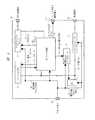
(実施の形態1)
図2〜図7により、本発明の実施の形態1の半導体装置の構成および動作の一例を説明する。図2は本実施の形態1の半導体装置のブロック図、図3はコンフィグ動作のタイミング図をそれぞれ示す。また、図4および図5は本実施の形態1における変形例、図6および図7は他の変形例をそれぞれ示す半導体装置のブロック図およびコンフィグ動作のタイミング図である。
【0027】
本実施の形態の半導体装置(LSI)は、たとえば図2に一例を示すように、LSI全体の演算処理を司るCPU1、不揮発性メモリであるフラッシュメモリ2、SRAM型FPGAであるプログラマブルロジック3、コンフィグ動作を司るコンフィグ回路4や、バスコントローラ5、割り込みコントローラ6、パワーオン検知回路7などから構成され、CPU1とフラッシュメモリ2とコンフィグ回路4とプログラマブルロジック3とバスコントローラ5がデータバスやアドレスバスなどにより構成されている内部バス11を介して接続され、プログラマブルロジック3とコンフィグ回路4がFPGAバス12を介して接続されている。更にコンフィグ回路4はコンフィグデータ転送のためにフラッシュメモリ2と専用のデータバス13を介して接続されている。更にプログラマブルロジック3とFPGAバス12及びアドレスバス16との接続部にセレクタを設け、内部バス11とFPGAバス12及びアドレスバス16とのバスセレクトが可能になるようにしても良い。コンフィグ動作時はFPGAバス12及びアドレスバス16が選択され、通常動作時は内部バス11が選択されるように構成する事も出来る。このような構成にすると、コンフィグ回路4はコンフィグ動作時のみ動作させ、それ以外の時はウェイト状態あるいは停止状態にして低消費電力化を図る事が出来る。
【0028】
このLSIには、外部端子として、リセット端子21、FPGA用端子22、外部端子23、コンフィグ完了検知端子24などがそれぞれ設けられている。リセット端子21はパワーオン検知回路7、FPGA用端子22はプログラマブルロジック3、外部端子23はバスコントローラ5、コンフィグ完了検知端子24はコンフィグ回路4にそれぞれ接続されている。更に外部端子23は外部のメモリや周辺LSIと接続可能で、データ信号、アドレス信号やチップセレクト信号等の制御信号を入出力することが可能である。
【0029】
コンフィグ回路4には、たとえばコンフィグ動作設定/制御回路、デコード回路、コンフィグスタートアドレス/転送データ量設定回路、周辺回路接続選択設定回路、リセット制御回路などが設けられている。コンフィグ動作設定/制御回路は、アドレスインクリメント、転送制御、各領域からコンフィグデータ読み出し/プログラマブルロジックへコンフィグデータ書き込み、コンフィグデータ転送量のカウント、コンフィグ完了フラグ、再コンフィグビット、コンフィグ完了時、割り込み要求/クリア制御などの各機能を備えている。デコード回路は、外部からの信号のデコード、回路内の内部信号のデコードなどの各機能を備えている。コンフィグスタートアドレス/転送データ量設定回路は、CPUにより書き換え可能なレジスタ群などを備えている。周辺回路接続選択設定回路は、CPUで書き換え可能であり、電源投入時はフラッシュメモリからコンフィグデータを読み出した後にさらに読み出してきたデータを自動設定する機能などを備えている。リセット制御回路は、電源投入後、コンフィグ動作に関係しないLSI内の各回路を制御するリセット信号を制御する機能などを備えている。
【0030】
このコンフィグ回路4は、割り込みコントローラ6に対して割り込み要求信号14を、CPU1、バスコントローラ5、割り込みコントローラ6に対して第2内部リセット信号19を、フラッシュメモリ2に対してアドレス15を、プログラマブルロジック3に対してアドレス16をそれぞれ供給する。また、コンフィグ回路4には、パワーオン検知回路7から第1内部リセット信号18が供給される。さらに、このコンフィグ回路4からは、コンフィグ動作設定レジスタ31に設定されたコンフィグ完了フラグがコンフィグ完了検知端子24を通じて外部に出力することも可能となっている。
【0031】
以上のように構成されるLSIにおいて、コンフィグ回路4によるコンフィグ動作は、CPU1による通常動作とは別に、たとえば図3に一例を示すようなタイミングとなる。
【0032】
(1)LSIに対してリセット端子21をアサートする。
【0033】
(2)パワーオン検知回路7がリセット信号を検知し、第1内部リセット信号18をアサートして発振安定時間待つ。
【0034】
(3)この時、コンフィグ回路4はパワーオン検知回路7から受けた第1内部リセット信号18を第2内部リセット信号19として、コンフィグ動作に関係しないLSI内の各モジュールに分配する。
【0035】
(4)発振安定時間が経過すると、パワーオン検知回路7が第1内部リセット信号18をネゲートする。
【0036】
(5)これにより、コンフィグに関係する回路が動作を開始し、専用データバス13、FPGAバス12を介して、コンフィグ回路4が自動的にアドレスバス15によって指定したフラッシュメモリ2内の決まった領域(アドレス)から決まった量のコンフィグデータをアドレスバス16によって指定したプログラマブルロジック3内の領域へ転送し、ロジックを構築する。この時、第2内部リセット信号19はアサートされたままになっている。
【0037】
(6)コンフィグ回路4によるコンフィグデータ転送が終わってプログラマブルロジック3内にロジックが構築できると、コンフィグ回路4内のコンフィグ動作設定レジスタ31のコンフィグ完了フラグが1にセットされる。
【0038】
(7)この時、第2内部リセット信号19もネゲートされ、通常のCPU1による動作が開始される。
【0039】
なお、以上のようなコンフィグ回路4によるコンフィグ動作のタイミングによって、以下のようなことも可能となる。
【0040】
(11)リセット端子21のネゲートは、コンフィグ動作が完了する前に行ってもよい。
【0041】
(12)CPU1が通常動作を開始したときには、既にプログラマブルロジック3内にロジックが構築されているので、プログラマブルロジック3に即座にアクセス、動作開始が可能である。
【0042】
(13)外部回路においては、たとえば図3に示すように、コンフィグ完了フラグの値をコンフィグ完了検知端子24から値を自動的に出力することにより、外部回路もFPGA用端子22へのアクセスが可能となったことを知ることができる。
【0043】
(14)本実施の形態において、コンフィグデータの格納領域は、通常、ユーザのプログラム/データが格納されているフラッシュメモリ2としたが、ユーザのプログラム/データが格納されているフラッシュメモリとコンフィグデータが格納されているフラッシュメモリがそれぞれ独立していても良い。これにより、たとえば高速動作が可能なプログラムは高価だが高速動作可能なフラッシュメモリの領域に、コンフィグデータの読み出しのように多少遅くてもよいデータは廉価なフラッシュメモリの領域に、という具合に区別することにより、LSIの最適化を図ることができる。
【0044】
(15)前記(11)において、リセット端子21のアサート後にフラッシュメモリ2の決まったアドレス(領域)からデータを読み出すのではなく、たとえば図3に示すように、まず最初にフラッシュメモリ2のある決まったアドレスから、ベクタフェッチの動作と同様な動作でコンフィグデータが格納されている最初のアドレス値を読み出し、そこからコンフィグデータを読み出してコンフィグ動作を行うような構成にしても良い。こうすると、ユーザが作成するプログラムにおいて、コンフィグデータを格納する領域の自由度が広がる。
【0045】
(16)パワーオン検知回路7はコンフィグ回路4の中に含めても良い。
【0046】
(17)コンフィグデータは専用バスによって転送されるだけでなく、内部バスを一時的に占有してコンフィグデータを転送可能にしても良い。
【0047】
コンフィグ回路4はプログラマブルロジック3に対するコンフィグデータ転送が終了した後には、内部バス11とプログラマブルロジック3とを接続させるためのブリッジ回路として機能しても良い。
【0048】
FPGAバス12はコンフィグデータ転送のためのバスとして機能するだけでなく、通常動作時においてもバスとして動作することが可能である。
【0049】
アドレスバス15はフラッシュメモリ2内の任意の領域に格納されたコンフィグ用データを転送するためのアドレス指定に用いることが可能である。
【0050】
アドレスバス16はコンフィグデータ以外のデータをプログラマブルロジック3の任意の領域に格納するためのアドレス指定のために利用しても良い。
【0051】
従って、本実施の形態によれば、▲1▼リセット入力は、発振安定時間を気にせずにいつでもネゲートできる、▲2▼発振安定時間経過後、特別な設定なしにプログラマブルロジック3に対するコンフィグ動作を自動的に行える、▲3▼コンフィグデータをフラッシュメモリ2の任意の場所に配置することができる、▲4▼CPU1が通常動作を開始する時には既にコンフィグ動作が完了しているので、すぐにプログラマブルロジック3にアクセスが可能である、▲5▼外部回路はコンフィグ動作が終了したことをコンフィグ完了検知端子24から確認できる、▲6▼コンフィグ動作のデータバス13を専用バス化することにより、バス制御を必要とすることなくコンフィグ動作を行うことができる、などの効果を得ることができる。
【0052】
次に、図4および図5により、本実施の形態1の変形例の半導体装置の構成および動作の一例を説明する。
【0053】
図4に示す半導体装置は、前記図2の構成からパワーオン検知回路7を削除した構成となっており、コンフィグ回路4によるコンフィグ動作は図5に示すようなタイミングとなる。
【0054】
(1)LSIに対してリセット端子21をアサートする。
【0055】
(2)リセット端子21からの入力は第1内部リセット信号18として、LSI内部の各モジュールに分配される。この時、コンフィグ動作に関係のない各モジュールに対しては、コンフィグ回路4が第2内部リセット信号19を分配する。
【0056】
(3)リセット端子21からの入力は、規定された発振安定時間以上アサートする。
【0057】
(4)発振安定時間以上経過したら、リセット端子21をネゲートする。
【0058】
(5)これを受けると、第1内部リセット信号18がネゲートされ、コンフィグ回路4が自動的にフラッシュメモリ2内の決まった領域(アドレス)から決まった量のコンフィグデータをプログラマブルロジック3へ転送し、ロジックを構築する。この時、依然として第2内部リセット信号19はアサートされたままになっており、コンフィグ動作に関係しないモジュールは動作を停止している。
【0059】
(6)コンフィグ回路4によるコンフィグデータ転送が終わってプログラマブルロジック3内にロジックが構築できると、コンフィグ回路4内のコンフィグ動作設定レジスタ31のコンフィグ完了フラグが1にセットされる。
【0060】
(7)この時、コンフィグ回路4が第2内部リセット信号19をネゲートすることにより、CPU1が通常動作を開始する。
【0061】
なお、以上のようなコンフィグ回路4によるコンフィグ動作のタイミングにおいては、以下のようなことも可能である。
【0062】
(21)CPU1でコンフィグ完了フラグを読み出さなくても、コンフィグ完了フラグの値をコンフィグ完了検知端子24から値を自動的に出力することにより、外部回路もFPGA用端子22へのアクセスが可能となったことを知ることができる。また、コンフィグ動作が完了したら、コンフィグ回路4から割り込みコントローラ6へ割り込み要求信号14を発生させることによっても、コンフィグ動作が完了したことを知ることができる。
【0063】
(22)フラッシュメモリ2からコンフィグデータを読み出すときに使用するデータバスとして、CPU1などと共有している内部バス11ではなく、コンフィグデータ読み出し専用データバス13を設けても良い。
【0064】
(23)前記図3において示した(12)〜(15)の内容については同様に当てはまる。
【0065】
従って、本実施の形態1の変形例によれば、▲1▼リセットアサート後、特別な設定をせずにプログラマブルロジック3に対するコンフィグ動作を自動的に行える、▲2▼コンフィグデータをフラッシュメモリ2の任意の場所に配置することができる、▲3▼CPU1が通常動作を開始する時には既にコンフィグ動作が完了しているので、すぐにプログラマブルロジック3にアクセスが可能である、▲4▼外部回路はコンフィグ動作が終了したことをコンフィグ完了検知端子24から確認できる、▲5▼コンフィグ動作のデータバス13を専用バス化することにより、バス制御を必要とすることなくコンフィグ動作を行うことができる、などの効果を得ることができる。
【0066】
次に、図6および図7により、本実施の形態1の他の変形例の半導体装置の構成および動作の一例を説明する。
【0067】
図6に示す半導体装置は、前記図4と同じ構成において、コンフィグ回路4が第2内部リセット信号19を生成する代わりに、リセット端子21からの入力信号により制御するような構成となっており、コンフィグ回路4によるコンフィグ動作は図7に示すようなタイミングとなる。
【0068】
(1)LSIに対してリセット端子21をアサートする。
【0069】
(2)リセット端子21からの入力は第1内部リセット信号18として、LSI内部の各モジュールに分配される。
【0070】
(3)リセット端子21からの入力は、規定された発振安定時間以上アサートする。
【0071】
(4)発振安定時間以上経過したら、リセット端子21をネゲートする。
【0072】
(5)これを受け、CPU1による通常動作が開始されるとともに、コンフィグ回路4が自動的にフラッシュメモリ2内の決まった領域(アドレス)から決まった量のコンフィグデータをプログラマブルロジック3へ転送し、ロジックを構築する。
【0073】
(6)コンフィグ回路4によるコンフィグデータ転送が終わってプログラマブルロジック3内にロジックが構築できると、コンフィグ回路4内のコンフィグ動作設定レジスタ31のコンフィグ完了フラグが1にセットされる。
【0074】
なお、以上のようなコンフィグ回路4によるコンフィグ動作のタイミングにおいては、以下のようなことも可能である。
【0075】
(31)CPU1がコンフィグ完了フラグを読み出すことにより、LSIはプログラマブルロジック3へのアクセスが可能となったことを知ることができる。
【0076】
(32)コンフィグ回路4内に書き込み保護機能(ビット)を設け、コンフィグ動作を行っている最中はコンフィグ動作に関するレジスタの設定を上書きできないようにプロテクトする機能を設けても良い。
【0077】
(33)フラッシュメモリ2内の値はCPU1以外では読めないように、一度でも外部から読もうとすると、ALL“0”しか読めなくなってしまうようなプログラムプロテクト機能を有している場合もあるが、コンフィグデータに関しても同様に、コンフィグ動作中以外はプログラマブルロジック3内からFPGAバス12を経由してデータを読み出せないように制御する。すなわち、コンフィグ時におけるデータベリファイ以外では、FPGAバス12を経由してきたデータは内部バスに乗せないようにする機能を設け、セキュリティを強化しても良い。
【0078】
(34)前記図3において示した(12)〜(15)、前記図5において示した(21)〜(22)の内容については同様に当てはまる。
【0079】
従って、本実施の形態1の他の変形例によれば、▲1▼リセットアサート後、特別な設定を行うことなくプログラマブルロジック3に対するコンフィグ動作を自動的に行える、▲2▼コンフィグデータをフラッシュメモリ2の任意の場所に配置することができる、▲3▼コンフィグ動作が終了したことを、コンフィグ完了検知端子24から、あるいはレジスタ内のフラグの値を読み出すことによって確認できる、▲4▼コンフィグ動作のデータバス13を専用バス化することにより、CPU1などによる動作と並行してコンフィグ動作を行うことができる、などの効果を得ることができる。
【0080】
(実施の形態2)
図8および図9により、本発明の実施の形態2の半導体装置の構成および動作の一例を説明する。図8は本実施の形態2の半導体装置のブロック図、図9はコンフィグ動作のタイミング図をそれぞれ示す。
【0081】
本実施の形態の半導体装置(LSI)は、たとえば図8に一例を示すように、CPU1、フラッシュメモリ2、プログラマブルロジック3、コンフィグ回路4、バスコントローラ5などから構成され、前記実施の形態1との相違点は、コンフィグ回路4内にコンフィグデータの読み出し先アドレスを設定するレジスタがあり、また外部からリセット端子をアサートしなくてもコンフィグ回路4内のレジスタのあるビットに書き込みをすれば、コンフィグを再度行う機能を持つようにした点である。
【0082】
すなわち、このLSIのコンフィグ回路4には、コンフィグ動作設定レジスタ31、コンフィグスタートアドレス設定レジスタ32、コンフィグデータ転送回数設定レジスタ33が設けられている。コンフィグ動作設定レジスタ31には、コンフィグ完了フラグの他に、コンフィグ開始ビット、再コンフィグビットが設定される。
【0083】
さらに、外部端子として、コンフィグ開始トリガ端子25が設けられ、このコンフィグ開始トリガ端子25からの入力によって、コンフィグ回路4のコンフィグ動作設定レジスタ31に再コンフィグビットが設定され、またリセット端子21からの入力とともにゲート回路で演算処理されてコンフィグ開始ビットが設定される。またこの動作はCPUからのプログラム制御により、FPGAでのデータ処理等を終わらせたうえで、コンフィグ開始ビットを設定することにより再びフラッシュメモリからFPGAへのコンフィグ動作が行われても良い。
【0084】
このような構成において、コンフィグ回路4によるコンフィグ動作(再コンフィグ時)は図9に示すようなタイミングとなる。
【0085】
(1)コンフィグ動作を開始するのは、▲1▼リセット端子21がアサートされた時、▲2▼コンフィグ開始トリガ端子25がアサートされた時、▲3▼CPU1が内部バス11を経由して、コンフィグ回路4内のコンフィグ動作設定レジスタ31内のコンフィグ開始ビットに設定を行った時、の各ケースである。上記▲1▼、▲2▼を行うと、コンフィグ開始ビットが自動的にセットされる。
【0086】
(2)上記▲2▼、▲3▼においては、コンフィグ回路4内のコンフィグ動作設定レジスタ31の再コンフィグビットも自動的にセットされる。ここで、再コンフィグビットがセットされた場合には、コンフィグ回路4内のコンフィグスタートアドレス設定レジスタ32からコンフィグデータを読み出すアドレスを読み出した後、その領域からデータを転送してコンフィグ動作を行う。
【0087】
(3)コンフィグ回路4内には、コンフィグスタートアドレス設定レジスタ32以外に、コンフィグデータ転送回数設定レジスタ33も存在している。これにより、プログラマブルロジック3内に構築する論理の規模によって可変であるコンフィグデータのデータ転送量を設定することができるため、プログラマブルロジック3内の一部の論理だけを再構築することができる。
【0088】
(4)本実施の形態においても、前記実施の形態1で説明した機能が設けられていても構わない。
【0089】
従って、本実施の形態2によれば、▲1▼リセット解除後の通常動作中に再度、コンフィグ動作が行える、▲2▼再コンフィグ動作は、コンフィグ開始トリガ端子25からのトリガ信号入力か、あるいはCPU1などを用いてビットを設定することにより実現できる、▲3▼コンフィグデータの格納場所を、アドレスマップされた全領域に広げることができる、▲4▼コンフィグデータ量を任意に設定できるため、プログラマブルロジック3を一部だけ再構築することが可能となる、などの効果を得ることができる。
【0090】
(実施の形態3)
図10により、本発明の実施の形態3の半導体装置の構成および動作の一例を説明する。図10は本実施の形態3の半導体装置のブロック図を示す。
【0091】
本実施の形態の半導体装置(LSI)は、たとえば図10に一例を示すように、CPU1、フラッシュメモリ2、プログラマブルロジック3、コンフィグ回路4、バスコントローラ5などから構成され、前記実施の形態1および2との相違点は、コンフィグデータが格納されているアドレスを予め複数設定可能であり、実際にどのアドレスからコンフィグデータを読み出すかの制御については外部端子から、あるいはコンフィグ回路4内のレジスタを設定することによって実現されるようにした点である。
【0092】
すなわち、このLSIのコンフィグ回路4には、コンフィグ動作設定レジスタ31、複数のコンフィグスタートアドレス設定レジスタ32a,32b,…およびコンフィグデータ転送回数設定レジスタ33a,33b,…、コンフィグアドレス選択レジスタ34、デコード回路35が設けられている。コンフィグ動作設定レジスタ31には、コンフィグ完了フラグ、コンフィグ開始ビット、再コンフィグビットの他に、チェーン設定ビットが格納される。コンフィグアドレス選択レジスタ34には、アドレスレジスタ選択、端子/レジスタ設定選択のビットが設定される。これらコンフィグスタートアドレス設定レジスタ32a,32b,…、コンフィグデータ転送回数設定レジスタ33a,33b,…に設定するための値は予めCPU等の制御によって設定しておく必要がある。
【0093】
さらに、外部端子として、転送アドレス選択端子26〜28が設けられ、この転送アドレス選択端子26〜28からの入力信号をデコード回路35によってデコードし、各コンフィグスタートアドレス設定レジスタ32a,32b,…、コンフィグデータ転送回数設定レジスタ33a,33b,…の選択制御を行う。また、この各コンフィグスタートアドレス設定レジスタ32a,32b,…、コンフィグデータ転送回数設定レジスタ33a,33b,…を選択する制御としては前記転送アドレス選択端子26〜28のみでなく、コンフィグ回路内のコンフィグアドレス選択レジスタ34によっても選択することが可能となる。
【0094】
このような構成において、コンフィグ回路4によるコンフィグ動作は前記実施の形態1および2と同様のタイミングとなる。
【0095】
(1)コンフィグ回路4内には、多数のコンフィグスタートアドレス設定レジスタ32a,32b,…と、コンフィグデータ転送回数設定レジスタ33a,33b,…があり、それらの設定によりコンフィグ動作を開始する時に、どこの領域にあるデータをコンフィグデータとして転送するか、選択することが可能となる。ここで、コンフィグスタートアドレス設定レジスタ32a,32b,…と、コンフィグデータ転送回数設定レジスタ33a,33b,…は、予めCPU1などを用いて値を設定しておく必要がある。
【0096】
(2)ここで、前記実施の形態2の手順(1)の▲2▼、▲3▼の時、転送アドレスレジスタ選択端子26〜28の設定によって、多種類(例えば本例では3本の選択端子からの信号による3ビットで最大8種類)のコンフィグスタートアドレス/転送回数設定を選択することができる。
【0097】
(3)上記(2)の設定では、外部端子からではなく、コンフィグ回路4内に設けられたコンフィグアドレス選択レジスタ34によっても選択することができる。この時、コンフィグアドレス選択レジスタ34で設定した値は転送アドレスレジスタ選択端子26〜28の入力値をデコードするデコード回路35内に入力され、転送アドレスレジスタ選択端子26〜28の設定か、あるいはコンフィグアドレス選択レジスタ34の設定値かを選ぶことができる。
【0098】
(4)前記実施の形態2までは、コンフィグデータはあるアドレス領域から連続したデータを1回だけ転送してプログラマブルロジック3内にロジックを構築していたが、コンフィグしたいデータが空間として不連続なアドレスに存在した場合、コンフィグスタートアドレス設定レジスタ32a,32b,…/コンフィグデータ転送回数設定レジスタ33a,33b,…をそれぞれのレジスタで設計された分だけ順番に転送を行なっていく事により対応出来る。このように、いくつかのレジスタで設定された内容通りに順番に転送していく、いわゆるチェーン動作の設定は、コンフィグ回路4内のコンフィグ動作設定レジスタ31で行えば良い。
【0099】
(5)本実施の形態においても、前記実施の形態1および2で説明した機能が設けられていても構わない。
【0100】
従って、本実施の形態3によれば、▲1▼再コンフィグを行う際、予め設定した多くのアドレス値の中から状況に応じて任意のコンフィグデータをコンフィグすることができる、▲2▼コンフィグデータがアドレス的に連続していなくても、連続したコンフィグ動作を行うことができる、などの効果を得ることができる。
【0101】
(実施の形態4)
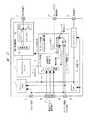
図11および図12により、本発明の実施の形態4の半導体装置の構成および動作の一例を説明する。図11は本実施の形態4の半導体装置のブロック図、図12はコンフィグ動作のタイミング図をそれぞれ示す。
【0102】
本実施の形態の半導体装置(LSI)は、たとえば図11に一例を示すように、CPU1、フラッシュメモリ2、プログラマブルロジック3、コンフィグ回路4、バスコントローラ5、CMT41、SCIF42、MTU43、周辺回路接続信号セレクタ回路44などから構成され、前記実施の形態1〜3との相違点は、プログラマブルロジック3とLSI内部の各種信号を接続有効/無効の切り替えが自動的になされる回路を持ち、また接続信号はいくつかの信号とマルチプレクスされており、選択することが可能なようにした点である。更に周辺回路であるCMT41、SCIF42、MTU43は内部バス11と接続可能な構成となっており、CPU1等からの制御が可能となる。
【0103】
すなわち、このLSIにおいて、CMT41はコンペア・マッチ・タイマ、SCIF42はシリアル・コミュニケーション・インタフェース、MTU43はマルチファンクション・タイマパルス・ユニットである。
【0104】
また、周辺回路接続信号セレクタ回路44には、たとえばFPGA入力側セレクト回路、FPGA出力側セレクト回路、周辺回路接続有効/無効制御回路などが設けられている。FPGA入力側セレクト回路は、周辺回路からプログラマブルロジック3への接続信号をコンフィグ回路内の周辺回路接続選択設定回路により選択する機能などを備えている。FPGA出力側セレクト回路は、プログラマブルロジック3から周辺回路への接続信号をコンフィグ回路内の周辺回路接続選択設定回路により選択する機能などを備えている。周辺回路接続有効/無効制御回路は、コンフィグ動作中は接続信号を無効にして、周辺回路が誤動作しないようにする機能などを備えている。
【0105】
さらに、このLSIのコンフィグ回路4には、コンフィグ動作設定レジスタ31、デコード回路35などの他に、セレクタ制御レジスタ36が設けられている。
【0106】
このような構成において、コンフィグ回路4によるコンフィグ動作は図12に示すようなタイミングとなる。
【0107】
(1)▲1▼リセット端子21のアサート、▲2▼コンフィグ開始トリガ端子25のアサート、▲3▼コンフィグ回路4内のコンフィグ動作設定レジスタ31のコンフィグ開始ビット(再コンフィグビットは自動的にセット)のいずれかを行うと、コンフィグ動作を開始する。
【0108】
(2)コンフィグ動作を行っている最中は、プログラマブルロジック3とCMT41、SCIF42、MTU43などのLSI内モジュールとの接続信号が無効であるように、周辺回路接続信号セレクタ回路44が制御を行う(接続信号をネゲート状態に保つ)。
【0109】
(3)コンフィグ動作が完了すると、コンフィグ回路4内のコンフィグ動作設定レジスタ31のコンフィグ完了フラグがセットされるが、これと同時に接続信号有効ビットもセットされる。周辺回路接続信号セレクタ回路44は接続信号有効ビットがセットされたのを受けて、自動的に各モジュールとの接続信号を有効状態にする。
【0110】
(4)再コンフィグの際には、接続信号有効ビットの値は自動的にクリアされ、周辺接続信号有効ビットを無効状態(ネゲート状態)に保つ。
【0111】
なお、以上のようなコンフィグ回路4によるコンフィグ動作においては、以下のようなことも可能である。
【0112】
(41)プログラム開発後は、プログラマブルロジック3のどの内部I/Oをどのモジュールと接続するかが決定されているが、開発段階では、それが決定していない。ここで、もしプログラマブルロジック3の内部I/OとCMT41、SCIF42、MTU43のようなLSI内のモジュールと接続が一意に決まっているとすると、プログラマブルロジック3に構築するロジックにI/Oの配置制限が加わることになり、プログラマブルロジック3の設計自由度が下がる。そこで、どのプログラマブルロジック3の内部I/OをCMT41、SCIF42、MTU43などに接続すればいいかを選択する機能を設けることにより、プログラマブルロジック3のI/O配置制限を緩和することができる。
【0113】
(42)周辺回路接続信号セレクタ回路44での選択は、コンフィグ回路4内のセレクタ制御レジスタ36に値を書き込むことによって実現される。これは、コンフィグ動作を行う時に、コンフィグ回路4内のセレクタ制御レジスタ36に値を書き込む(つまりデータを転送する)よう、コンフィグデータにデータを追加しておくだけで良い。
【0114】
(43)セレクタ制御レジスタ36の値は、CPU1などを用いて通常動作中にセットしても良い。
【0115】
(44)接続信号有効ビットの値も、CPU1などを用いて通常動作中に書き換えしても良い。
【0116】
(45)本実施の形態においても、前記実施の形態1〜3で説明した機能が設けられていても構わない。
【0117】
従って、本実施の形態4によれば、▲1▼プログラマブルロジック3とCMT41、SCIF42、MTU43などのモジュールとの接続信号を、コンフィグ動作の最中では無効にし、さらにコンフィグが完了すると、自動的に接続信号を有効状態に切り替えることができる、▲2▼プログラマブルロジック3と各モジュールの接続信号をセレクタ制御レジスタ36の設定によって切り替えられるようにして、プログラマブルロジック3のI/O割り当て制限を緩和できる、などの効果を得ることができる。
【0118】
(実施の形態5)
図13により、本発明の実施の形態5の半導体装置の構成および動作の一例を説明する。図13は本実施の形態5の半導体装置のブロック図を示す。
【0119】
本実施の形態の半導体装置(LSI)は、たとえば図13に一例を示すように、CPU1、フラッシュメモリ2、プログラマブルロジック3、コンフィグ回路4、バスコントローラ5、端子制御回路51などから構成され、前記実施の形態1〜4との相違点は、FPGA用端子22を制御することが可能な端子制御回路51を持つようにした点である。
【0120】
すなわち、このLSIにおいて、端子制御回路51には、たとえばプルアップ/プルダウン回路52、このプルアップ/プルダウン回路52の制御回路53などが設けられている。プルアップ/プルダウン回路52は、各端子において、コンフィグ動作時に端子の電圧レベルを制御する機能、電源投入後、コンフィグ動作が完了するまでは電圧レベルをハイにしておく(プルアップMOSFETを有効)機能などを備えている。
【0121】
更に、プルアップ/プルダウン回路52は、プルアップMOSFET52aとプルダウンMOSFET52bなどからなり、それぞれ制御回路53によりゲート制御され、またプルアップMOSFET52aのソースは電源電位に、プルダウンMOSFET52bのソースは接地電位にそれぞれ接続され、ドレインが共通に接続されてFPGA用端子22に接続されている。
【0122】
このような構成において、コンフィグ回路4によるコンフィグ動作は前記図12に示すようなタイミングとなる。
【0123】
(1)▲1▼リセット端子21のアサート、▲2▼コンフィグ開始トリガ端子25のアサート、▲3▼コンフィグ回路4内のコンフィグ動作設定レジスタ31のコンフィグ開始ビット(再コンフィグビットは自動的にセット)のいずれかを行うと、コンフィグ動作を開始する。
【0124】
(2)コンフィグ動作を行っている最中は、プログラマブルロジック3とFPGA用端子22の接続が無効であるように、端子制御回路51が制御を行う(接続信号をネゲート状態に保つ)。
【0125】
(3)コンフィグ動作が完了すると、コンフィグ回路4内のコンフィグ完了フラグと接続信号有効ビットがセットされる。端子制御回路51はこれを受けて、自動的にプログラマブルロジック3、及びFPGA用端子22との接続信号を有効状態にする。
【0126】
(4)再コンフィグの際には、接続信号有効ビットの値は自動的にクリアされ、再び接続信号を無効状態(ネゲート状態)に保つ。
【0127】
なお、以上のようなコンフィグ回路4によるコンフィグ動作においては、以下のようなことも可能である。
【0128】
(51)上記(2)において、FPGA用端子22はLSIにとって入力か出力か、ハイアクティブかローアクティブなのかはコンフィグが完了するまで分からない。そこで、端子制御回路51は端子がいずれの場合でも適応可能とするために、プルアップMOSFET52aを用意し、コンフィグが完了するまで、FPGA用端子22はこのプルアップMOSFET52aにより1をドライブするようにしておく。コンフィグが完了したら、プルアップMOSFET52aの動作を無効にし、プログラマブルロジック3とFPGA用端子22を接続した状態(有効な状態)にする。
【0129】
(52)場合によっては、FPGA用端子22に対して、プルダウンMOSFET52bを接続して0をドライブしたい場合もあり得る。この場合、コンフィグ回路4内のFPGA用端子コントロールレジスタに値を設定することにより、プルアップMOSFET52aを無効にして、プルダウンMOSFET52bを有効にするように切り替える。
【0130】
(53)上記(52)の設定は、▲1▼通常動作中にCPU1などによる設定と、▲2▼コンフィグ動作中にコンフィグデータとともに、FPGA用端子コントロールレジスタに設定が行われるように、コンフィグデータに設定値を追加しておく、の2通りが考えられる。
【0131】
(54)電源投入直後から端子レベルをプルダウン設定することができないが、通常動作中に再コンフィグを行いたい時などに端子状態を固定させるときに有効となる。
【0132】
(55)本実施の形態においても、前記実施の形態1〜4で説明した機能が設けられていても構わない。
【0133】
従って、本実施の形態5によれば、▲1▼プログラマブルロジック3と外部端子との接続信号を、コンフィグ動作の最中は無効にし、さらにコンフィグが完了すると、自動的に接続信号を有効状態に切り替えることができる、▲2▼コンフィグ最中はプルアップMOSFET52aを動作させることにより、他のLSIに悪影響を与えないようにすることができる、▲3▼プルアップMOSFET52aではなく、プルダウンMOSFET52bが必要な場合には、レジスタに値を設定することによって切り替えることにより、再コンフィグなどの時、端子状態の電圧レベルをハイ/ローどちらかに任意に固定させることができる、などの効果を得ることができる。
【0134】
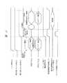
以上、実施の形態1〜5で説明したようなLSIのアプリケーションとしては、たとえば図14に一例を示すように、ロジック(1)+ロジック(2)+ロジック(3)≧プログラマブルロジック3の規模であっても、時間的に必要なロジックのみを動的にプログラマブルロジック3内に再コンフィグしていくことにより、プログラマブルロジック3の節約、具体的にはチップ面積の縮小による売価の低価格化および不良率の低減などが可能となる。
【0135】
さらに、チップ内部に格納したコンフィグ用データを必要に応じて選択的にFPGAに対して転送制御を行うコンフィグ回路を有することにより、他のアプリケーションとして、たとえば図15に一例を示すように、一般的には、産業向け、通信向け、ASICなどのように、それぞれのユーザに合ったロジックをソフトウェア(プログラム)のみで作成可能であり、さらにそれらによって、部品点数が増えない、1チップのままで対応することが可能となる。
【0136】
以上で述べた実施の形態において、コンフィグ回路4はプログラマブルロジック3に対するコンフィグデータ転送が終了した後には、内部バス11とプログラマブルロジック3とを接続させるためのブリッジ回路として機能しても良い。
【0137】
FPGAバス12はコンフィグデータ転送のためのバスとして機能するだけでなく、通常動作時においてもバスとして動作することが可能である。
【0138】
アドレスバス15はフラッシュメモリ2内の任意の領域に格納されたコンフィグ用データを転送するためのアドレス指定に用いることが可能である。
【0139】
アドレスバス16はコンフィグデータ以外のデータをプログラマブルロジック3の任意の領域に格納するためのアドレス指定のために利用しても良い。
【0140】
コンフィグデータは専用データバス13を介してだけでなく、内部バス11を介することによってもプログラマブルロジック3に対して転送することが可能である。
【0141】
プログラマブルロジック3に接続されたFPGA端子22と外部に接続されたデバイスとの接続は、バス接続が可能となるように接続されてあっても良いし、信号線によって接続されてあっても良い。つまり、プログラマブルロジック3とFPGA端子22との接続はバス接続に限定されるだけでなく、制御信号線が接続されるようになっていても良い。
【0142】
更に、各実施例で示された内容は其々単独で実施することに限定されるだけでなく、其々を任意に組み合わせて実施されても良い。
【0143】
以上、本発明者によってなされた発明をその実施の形態に基づき具体的に説明したが、本発明は前記実施の形態に限定されるものではなく、その要旨を逸脱しない範囲で種々変更可能であることはいうまでもない。
【0144】
【発明の効果】
本願において開示される発明のうち、代表的なものによって得られる効果を簡単に説明すれば、以下のとおりである。
【0145】
(1)SRAM型FPGA内蔵LSIにおいて必須の動作であるコンフィグ動作を司る回路をハード化した事により、パワーオンリセット後のLSI立上げ期間が短く出来る。
【0146】
(2)コンフィグ動作プログラムが不要となる。
【0147】
(3)再コンフィグが容易にフレキシブルに行なえる。
【0148】
(4)コンフィグ動作が完了した事を外部に接続された回路が容易に知る事が出来る。
【図面の簡単な説明】
【図1】本発明において、コンフィグ動作における各リソース使用時の比較を示す説明図である。
【図2】本発明の実施の形態1の半導体装置を示すブロック図である。
【図3】本発明の実施の形態1の半導体装置において、コンフィグ動作を示すタイミング図である。
【図4】本発明の実施の形態1における変形例の半導体装置を示すブロック図である。
【図5】本発明の実施の形態1における変形例の半導体装置において、コンフィグ動作を示すタイミング図である。
【図6】本発明の実施の形態1における他の変形例の半導体装置を示すブロック図である。
【図7】本発明の実施の形態1における他の変形例の半導体装置において、コンフィグ動作を示すタイミング図である。
【図8】本発明の実施の形態2の半導体装置を示すブロック図である。
【図9】本発明の実施の形態2の半導体装置において、コンフィグ動作を示すタイミング図である。
【図10】本発明の実施の形態3の半導体装置を示すブロック図である。
【図11】本発明の実施の形態4の半導体装置を示すブロック図である。
【図12】本発明の実施の形態4の半導体装置において、コンフィグ動作を示すタイミング図である。
【図13】本発明の実施の形態5の半導体装置を示すブロック図である。
【図14】本発明の実施の形態の半導体装置におけるアプリケーションを示す説明図である。
【図15】本発明の実施の形態の半導体装置における他のアプリケーションを示す説明図である。
【符号の説明】
1 CPU
2 フラッシュメモリ
3 プログラマブルロジック
4 コンフィグ回路
5 バスコントローラ
6 割り込みコントローラ
7 パワーオン検知回路
11 内部バス
12 FPGAバス
13 専用データバス
14 割り込み要求信号
15,16 アドレス
18 第1内部リセット信号
19 第2内部リセット信号
21 リセット端子
22 FPGA用端子
23 外部端子
24 コンフィグ完了検知端子
25 コンフィグ開始トリガ端子
26〜28 転送アドレス選択端子
31 コンフィグ動作設定レジスタ
32 コンフィグスタートアドレス設定レジスタ
33 コンフィグデータ転送回数設定レジスタ
34 コンフィグアドレス選択レジスタ
35 デコード回路
41 CMT
42 SCIF
43 MTU
44 周辺回路接続信号セレクタ回路
51 端子制御回路
52 プルアップ/プルダウン回路
52a プルアップMOSFET
52b プルダウンMOSFET
53 制御回路[0001]
BACKGROUND OF THE INVENTION
The present invention relates to a semiconductor device, and more particularly to a technique effective when applied to a semiconductor device in which an SRAM type FPGA and a nonvolatile memory such as a flash memory are mounted together.
[0002]
[Prior art]
According to a study by the present inventor, the following technologies can be considered for LSIs such as microcomputers and electronic devices incorporating the LSIs.
[0003]
In recent years, in electronic devices with built-in microcomputers, in order to increase the program scale, shorten the product development period, improve device specifications, adjust control data, rewrite the microcomputer program in each process from development to trial production, production start-up, and mass production. Field programmability that is easy to adjust is required. In order to cope with this, a microcomputer in which a CPU and a flash memory are integrated into one chip has been developed.
[0004]
On the other hand, when a customer actually constructs a system, a field programmable gate array (on the customer system board) is used for fine tuning and customization of each signal that cannot be handled only by changing the software using flash memory. (FPGA), programmable logic device (PLD), etc. are mounted and connected to the LSI on the substrate. FPGAs and PLDs are devices that allow a user to build a logic circuit on an LSI in a very short time based on a high-level description language or a logic circuit diagram, and are highly convenient.
[0005]
As a technique for mounting an LSI and an FPGA on such a user board, for example, a technique described in JP-A-5-233844 can be cited. This publication discloses a semiconductor device including an SRAM FPGA that forms a logic circuit by writing construction data, and a PROM that stores construction data that configures the logic circuit in the SRAM FPGA.
[0006]
[Problems to be solved by the invention]
By the way, as a result of examination by the present inventor on the technology for mounting the LSI and the FPGA on the user board as described above, the following has been clarified.
[0007]
For example, as described above, in the technique of separately mounting an LSI and an FPGA on a user board, (1) an increase in cost due to an increase in the number of parts on the user system and an increase in development period due to complicated board design, 2) Increased wiring delay caused by wiring on the board and reduced performance / quality resulting from reduced noise resistance, 3) Increased development costs by developing / evaluating separate chips, etc. There is a problem.
[0008]
The technique described in Japanese Patent Laid-Open No. 5-233844 is a technique for storing SRAM type FPGA construction data in a PROM, not a technique for storing it in a flash memory.
[0009]
Therefore, the present inventor, by incorporating an FPGA in an LSI equipped with a flash memory, enables fine tuning and customization of each signal that cannot be dealt with only by software changes at the time of system construction, which was difficult in the past. It has been found that a user can assemble a logic circuit on an LSI in a very short time, and an LSI with high convenience can be realized. Furthermore, since it is an SRAM type FPGA, it is necessary to construct an FPGA logic every time the power is turned on. By mounting a circuit for data transfer control for this construction in the same chip, it is possible to improve efficiency. It is possible to construct a typical FPGA logic.
[0010]
In this way, mounting flash memory and FPGA in one chip means that both software field programmability and hardware field programmability can be realized on one chip, and the user has control over it. It becomes easier. Furthermore, by installing a control circuit for transferring FPGA construction data from the built-in flash memory in the same chip, control for construction can be performed more efficiently.
[0011]
In addition, when using an FPGA whose logic is initialized every time the power is turned on on the user board, the FPGA logic must be constructed every time the power is turned on. Since the logic construction data passes on the board, the confidentiality is extremely low. In other words, it can be said that the security is weak.
[0012]
However, if a flash memory is installed and logic building data is built in the memory, and if a control circuit for controlling the transfer of the logic building data is built in, the logic building data is read from the flash memory. It can be transferred to the built-in FPGA without going through the outside of the LSI, the logic can be built in the FPGA without the data outside the LSI, and the confidentiality of the customized logic in the FPGA is maintained. It is very effective when you have to.
[0013]
SUMMARY OF THE INVENTION An object of the present invention is to provide a semiconductor device in which an SRAM FPGA, a nonvolatile memory such as a flash memory, and a data transfer control circuit for constructing the FPGA are mixedly mounted in an LSI in a very short time. Another object is to provide a semiconductor device in which a logic circuit can be assembled and a highly convenient LSI can be realized.
[0014]
The above and other objects and novel features of the present invention will be apparent from the description of this specification and the accompanying drawings.
[0015]
[Means for Solving the Problems]
Of the inventions disclosed in the present application, the outline of typical ones will be briefly described as follows.
[0016]
That is, the present invention relates to a CPU, an SRAM type FPGA that constitutes a logic circuit by writing construction data, a nonvolatile memory that stores construction data that constitutes a logic circuit in the SRAM type FPGA, and a memory stored in the nonvolatile memory. This construction data is applied to a semiconductor device having a configuration circuit that controls a configuration operation for an SRAM type FPGA, and has the following characteristics.
[0017]
(1) The configuration circuit has a function of transferring the FPGA construction data in the nonvolatile memory in the same chip to the SRAM type FPGA at the time of power-on reset. Furthermore, the configuration circuit has a function of canceling the internal reset signal after the completion of the configuration operation, or a terminal or signal for detecting the completion of the configuration operation by the configuration circuit is provided. It has a function to start, and is applied especially to a nonvolatile memory such as a flash memory.
[0018]
(2) The configuration circuit has a function of reconstructing a part of the construction data in the SRAM type FPGA transferred from the nonvolatile memory during normal operation.
[0019]
(3) A plurality of terminals or construction data selection transfer control mode selection signals corresponding to the construction data of the SRAM type FPGA are provided, and the configuration circuit is a nonvolatile memory corresponding to each of the plurality of terminals or construction data selection control mode selection signals. The construction data is selected and transferred to the SRAM type FPGA, and is applied particularly to a nonvolatile memory such as a flash memory.
[0020]
(4) A register for storing a plurality of transfer control information corresponding to the construction data of the SRAM type FPGA is provided, and the configuration circuit stores the construction data in the nonvolatile memory corresponding to each of the plurality of transfer control information stored in the register. Is selected and transferred to the SRAM-type FPGA, and is applied particularly to a nonvolatile memory such as a flash memory.
[0021]
DETAILED DESCRIPTION OF THE INVENTION
Hereinafter, embodiments of the present invention will be described in detail with reference to the drawings. Note that components having the same function are denoted by the same reference symbols throughout the drawings for describing the embodiments, and the repetitive description thereof will be omitted.
[0022]
The present invention is applied to a semiconductor device in which an SRAM type FPGA and a nonvolatile memory such as a flash memory are mounted together. Therefore, (1) SRAM-type FPGAs usually perform the first configuration operation (logic is built in the FPGA) when the power is turned on, and (2) data for first configuration in the FPGA is a non-volatile memory ( From the viewpoint that, for example, flash memory is normally stored in the same manner as a normal CPU operation program, and (3) configuration operation can be performed during normal operation. In the embodiment, in the FPGA + nonvolatile memory built-in LSI described above, a dedicated configuration circuit is mounted therein, and its operation is presented.
[0023]
Providing a dedicated configuration circuit as in the present invention has several advantages. For example, FIG. 1 shows a comparison when each resource (CPU, DMAC, config circuit) is used in the config operation. In the present invention, a dedicated hardware form called a configuration circuit is used, but by installing the dedicated configuration circuit, (1) an SRAM type FPGA is shown to be a hard logic because no program intervention by the CPU is required. (2) It is possible to obtain a great advantage such as being able to be regarded as a nonvolatile FPGA by the configuration of the built-in flash memory and the configuration circuit.
[0024]
Specifically, in the case of a configuration circuit, the startup time is faster than that of the CPU or DMAC (setting is not required), the program is unnecessary, and the configuration timing can be performed during or after resetting. As a result, the construction data in the nonvolatile memory can be transferred to the FPGA without waiting for the transfer control from the CPU at the time of power-on reset, compared with the case where the construction data of the logic circuit is transferred by the CPU or DMAC. It becomes possible to use a circuit built in the FPGA immediately after resetting.
[0025]
In the following, according to the present invention, a non-volatile memory such as a CPU, an SRAM type FPGA that constitutes a logic circuit by writing construction data, and a flash memory that stores construction data that constitutes the logic circuit in this SRAM type FPGA. An embodiment of a semiconductor device having a configuration circuit that controls a configuration operation for an SRAM type FPGA using construction data stored in the nonvolatile memory will be specifically described.
[0026]
(Embodiment 1)
An example of the configuration and operation of the semiconductor device according to the first embodiment of the present invention will be described with reference to FIGS. FIG. 2 is a block diagram of the semiconductor device according to the first embodiment, and FIG. 3 is a timing diagram of the configuration operation. 4 and FIG. 5 are a block diagram of a semiconductor device and a timing diagram of a configuration operation showing a modification example of the first embodiment, and FIGS. 6 and 7 are other modification examples, respectively.
[0027]
The semiconductor device (LSI) of this embodiment includes, for example, as shown in FIG. 2, a CPU 1 that performs arithmetic processing of the entire LSI, a
[0028]
This LSI is provided with a
[0029]
The
[0030]
This
[0031]
In the LSI configured as described above, the configuration operation by the
[0032]
(1) Assert the
[0033]
(2) The power-on detection circuit 7 detects the reset signal, asserts the first
[0034]
(3) At this time, the
[0035]
(4) When the oscillation stabilization time has elapsed, the power-on detection circuit 7 negates the first
[0036]
(5) Thereby, a circuit related to the configuration starts to operate, and a predetermined area in the
[0037]
(6) When the configuration data transfer by the
[0038]
(7) At this time, the second
[0039]
Note that the following is also possible depending on the timing of the configuration operation by the
[0040]
(11) The negation of the
[0041]
(12) When the CPU 1 starts normal operation, since the logic has already been built in the
[0042]
(13) In the external circuit, for example, as shown in FIG. 3, by automatically outputting the value of the configuration completion flag from the configuration
[0043]
(14) In the present embodiment, the configuration data storage area is normally the
[0044]
(15) In the above (11), instead of reading data from a predetermined address (area) of the
[0045]
(16) The power-on detection circuit 7 may be included in the
[0046]
(17) The configuration data may be transferred not only by the dedicated bus, but also the configuration data can be transferred by temporarily occupying the internal bus.
[0047]
The
[0048]
The
[0049]
The address bus 15 can be used for address designation for transferring configuration data stored in an arbitrary area in the
[0050]
The
[0051]
Therefore, according to this embodiment, (1) the reset input can be negated at any time without worrying about the oscillation stabilization time. (2) After the oscillation stabilization time has elapsed, the configuration operation for the
[0052]
Next, an example of the configuration and operation of the semiconductor device according to the modification of the first embodiment will be described with reference to FIGS.
[0053]
The semiconductor device shown in FIG. 4 has a configuration in which the power-on detection circuit 7 is deleted from the configuration of FIG. 2, and the configuration operation by the
[0054]
(1) Assert the
[0055]
(2) The input from the
[0056]
(3) The input from the
[0057]
(4) When the oscillation stabilization time has elapsed, the
[0058]
(5) Upon receiving this, the first
[0059]
(6) When the configuration data transfer by the
[0060]
(7) At this time, the
[0061]
Note that the following is also possible at the timing of the configuration operation by the
[0062]
(21) Even if the CPU 1 does not read the configuration completion flag, the external circuit can also access the
[0063]
(22) As a data bus used when reading configuration data from the
[0064]
(23) The contents of (12) to (15) shown in FIG.
[0065]
Therefore, according to the modification of the first embodiment, <1> after the reset is asserted, the configuration operation for the
[0066]
Next, referring to FIGS. 6 and 7, an example of the configuration and operation of a semiconductor device according to another modification of the first embodiment will be described.
[0067]
The semiconductor device shown in FIG. 6 has the same configuration as in FIG. 4, but the
[0068]
(1) Assert the
[0069]
(2) The input from the
[0070]
(3) The input from the
[0071]
(4) When the oscillation stabilization time has elapsed, the
[0072]
(5) Upon receipt of this, normal operation by the CPU 1 is started, and the
[0073]
(6) When the configuration data transfer by the
[0074]
Note that the following is also possible at the timing of the configuration operation by the
[0075]
(31) When the CPU 1 reads the configuration completion flag, the LSI can know that the
[0076]
(32) A write protection function (bit) may be provided in the
[0077]
(33) Although the value in the
[0078]
(34) The contents of (12) to (15) shown in FIG. 3 and (21) to (22) shown in FIG. 5 are similarly applied.
[0079]
Therefore, according to another modification of the first embodiment, (1) after the reset is asserted, the configuration operation for the
[0080]
(Embodiment 2)
An example of the configuration and operation of the semiconductor device according to the second embodiment of the present invention will be described with reference to FIGS. FIG. 8 is a block diagram of the semiconductor device according to the second embodiment, and FIG. 9 is a timing diagram of the configuration operation.
[0081]
The semiconductor device (LSI) of the present embodiment is composed of a CPU 1, a
[0082]
That is, the
[0083]
Further, a configuration
[0084]
In such a configuration, the configuration operation (at the time of reconfiguration) by the
[0085]
(1) The configuration operation is started when (1) the
[0086]
(2) In the above (2) and (3), the reconfiguration bit of the configuration
[0087]
(3) In the
[0088]
(4) Also in the present embodiment, the function described in the first embodiment may be provided.
[0089]
Therefore, according to the second embodiment, (1) the configuration operation can be performed again during the normal operation after the reset is released. (2) The reconfiguration operation is performed by inputting a trigger signal from the configuration
[0090]
(Embodiment 3)
An example of the configuration and operation of the semiconductor device according to the third embodiment of the present invention will be described with reference to FIG. FIG. 10 is a block diagram of the semiconductor device according to the third embodiment.
[0091]
The semiconductor device (LSI) of the present embodiment is composed of a CPU 1, a
[0092]
That is, the
[0093]
Further, transfer
[0094]
In such a configuration, the configuration operation by the
[0095]
(1) The
[0096]
(2) Here, in the steps (2) and (3) of the procedure (1) of the second embodiment, there are many types (for example, three selections in this example) depending on the setting of the transfer address
[0097]
(3) In the setting of (2) above, the selection can be made not by an external terminal but also by the configuration address selection register 34 provided in the
[0098]
(4) Up to the second embodiment, the configuration data is transferred only once from a certain address area and the logic is built in the
[0099]
(5) Also in the present embodiment, the functions described in the first and second embodiments may be provided.
[0100]
Therefore, according to the third embodiment, (1) when reconfiguring, arbitrary configuration data can be configured from a number of preset address values according to the situation. (2) Configuration data Even if the addresses are not continuous in terms of address, it is possible to obtain an effect such that a continuous configuration operation can be performed.
[0101]
(Embodiment 4)
An example of the configuration and operation of the semiconductor device according to the fourth embodiment of the present invention will be described with reference to FIGS. FIG. 11 is a block diagram of the semiconductor device according to the fourth embodiment, and FIG. 12 is a timing diagram of the configuration operation.
[0102]
The semiconductor device (LSI) of this embodiment includes, for example, a CPU 1, a
[0103]
That is, in this LSI,
[0104]
The peripheral circuit connection
[0105]
Furthermore, the
[0106]
In such a configuration, the configuration operation by the
[0107]
(1) (1) Assert reset
[0108]
(2) During the configuration operation, the peripheral circuit connection
[0109]
(3) When the configuration operation is completed, the configuration completion flag of the configuration
[0110]
(4) At the time of reconfiguration, the value of the connection signal valid bit is automatically cleared, and the peripheral connection signal valid bit is kept in an invalid state (negate state).
[0111]
In the configuration operation by the
[0112]
(41) After the program development, it is determined which internal I / O of the
[0113]
(42) Selection in the peripheral circuit connection
[0114]
(43) The value of the selector control register 36 may be set during normal operation using the CPU 1 or the like.
[0115]
(44) The value of the connection signal valid bit may be rewritten during normal operation using the CPU 1 or the like.
[0116]
(45) Also in the present embodiment, the functions described in the first to third embodiments may be provided.
[0117]
Therefore, according to the fourth embodiment, (1) the connection signal between the
[0118]
(Embodiment 5)
An example of the configuration and operation of the semiconductor device according to the fifth embodiment of the present invention will be described with reference to FIG. FIG. 13 is a block diagram of the semiconductor device according to the fifth embodiment.
[0119]
The semiconductor device (LSI) of the present embodiment is composed of a CPU 1, a
[0120]
That is, in this LSI, the
[0121]
Further, the pull-up / pull-down circuit 52 includes a pull-up MOSFET 52a and a pull-
[0122]
In such a configuration, the configuration operation by the
[0123]
(1) (1) Assert reset
[0124]
(2) During the configuration operation, the
[0125]
(3) When the configuration operation is completed, the configuration completion flag and the connection signal valid bit in the
[0126]
(4) At the time of reconfiguration, the value of the connection signal valid bit is automatically cleared, and the connection signal is kept in the invalid state (negate state) again.
[0127]
In the configuration operation by the
[0128]
(51) In the above (2), it is not known until the configuration is completed whether the
[0129]
(52) In some cases, it may be desired to connect the pull-
[0130]
(53) The setting of (52) is as follows: (1) Setting by the CPU 1 or the like during normal operation, and (2) Configuration data so that setting is performed in the FPGA terminal control register together with configuration data during configuration operation. There are two possible ways to add a set value to.
[0131]
(54) Although the terminal level cannot be pulled down immediately after the power is turned on, this is effective when the terminal state is fixed when reconfiguration is desired during normal operation.
[0132]
(55) Also in the present embodiment, the functions described in the first to fourth embodiments may be provided.
[0133]
Therefore, according to the fifth embodiment, (1) the connection signal between the
[0134]
As described above, as an LSI application as described in the first to fifth embodiments, for example, as shown in FIG. 14, the scale of logic (1) + logic (2) + logic (3) ≧
[0135]
Furthermore, by having a configuration circuit that selectively transfers the configuration data stored in the chip to the FPGA as needed, other applications such as the general example shown in FIG. Can create logic suitable for each user by software (program) only, such as for industrial, communication, ASIC, etc., and it can be handled as a single chip with no increase in the number of parts. It becomes possible to do.
[0136]
In the embodiment described above, the
[0137]
The
[0138]
The address bus 15 can be used for address designation for transferring configuration data stored in an arbitrary area in the
[0139]
The
[0140]
The configuration data can be transferred to the
[0141]
The connection between the
[0142]
Furthermore, the contents shown in each embodiment are not limited to being implemented independently, but may be implemented in any combination.
[0143]
As mentioned above, the invention made by the present inventor has been specifically described based on the embodiment. However, the invention is not limited to the embodiment, and various modifications can be made without departing from the scope of the invention. Needless to say.
[0144]
【The invention's effect】
Of the inventions disclosed in the present application, effects obtained by typical ones will be briefly described as follows.
[0145]
(1) Since the circuit for performing the configuration operation, which is an essential operation in the SRAM type LSI with built-in SRAM, is hardwareized, the LSI startup period after power-on reset can be shortened.
[0146]
(2) A configuration operation program is not required.
[0147]
(3) Reconfiguration can be performed easily and flexibly.
[0148]
(4) The externally connected circuit can easily know that the configuration operation has been completed.
[Brief description of the drawings]
FIG. 1 is an explanatory diagram showing a comparison when each resource is used in a configuration operation in the present invention.
FIG. 2 is a block diagram showing a semiconductor device according to the first embodiment of the present invention.
FIG. 3 is a timing chart showing a configuration operation in the semiconductor device according to the first embodiment of the present invention.
FIG. 4 is a block diagram showing a modified semiconductor device according to the first embodiment of the present invention.
FIG. 5 is a timing chart showing a configuration operation in the semiconductor device according to the modified example of the first embodiment of the present invention.
FIG. 6 is a block diagram showing another variation of the semiconductor device according to the first embodiment of the present invention.
FIG. 7 is a timing chart showing a configuration operation in a semiconductor device of another modification example in the first embodiment of the present invention;
FIG. 8 is a block diagram showing a semiconductor device according to a second embodiment of the present invention.
FIG. 9 is a timing chart showing a configuration operation in the semiconductor device according to the second embodiment of the present invention.
FIG. 10 is a block diagram showing a semiconductor device according to a third embodiment of the present invention.
FIG. 11 is a block diagram showing a semiconductor device according to a fourth embodiment of the present invention.
FIG. 12 is a timing chart showing a configuration operation in the semiconductor device according to the fourth embodiment of the present invention.
FIG. 13 is a block diagram showing a semiconductor device according to a fifth embodiment of the present invention.
FIG. 14 is an explanatory diagram showing an application in the semiconductor device according to the embodiment of the present invention;
FIG. 15 is an explanatory diagram showing another application in the semiconductor device according to the embodiment of the present invention;
[Explanation of symbols]
1 CPU
2 Flash memory
3 Programmable logic
4 Configuration circuit
5 Bus controller
6 Interrupt controller
7 Power-on detection circuit
11 Internal bus
12 FPGA bus
13 Dedicated data bus
14 Interrupt request signal
15,16 address
18 First internal reset signal
19 Second internal reset signal
21 Reset terminal
22 FPGA terminal
23 External terminal
24 Configuration completion detection terminal
25 Config start trigger terminal
26 to 28 Transfer address selection terminal
31 Config operation setting register
32 Config start address setting register
33 Configuration data transfer count setting register
34 Config address selection register
35 Decoding circuit
41 CMT
42 SCIF
43 MTU
44 Peripheral circuit connection signal selector circuit
51 terminal control circuit
52 Pull-up / pull-down circuit
52a Pull-up MOSFET
52b Pull-down MOSFET
53 Control circuit
Claims (4)
Translated fromJapanese前記SRAM型FPGAの構築データに対応する複数の端子を設け、前記コンフィグ回路は、前記複数の端子のそれぞれと対応する前記不揮発性メモリ内の構築データを選択して前記SRAM型FPGAに転送する機能を有することを特徴とする半導体装置。Using a CPU, an SRAM type FPGA that constitutes a logic circuit by writing construction data, a non-volatile memory that stores construction data that constitutes a logic circuit in the SRAM type FPGA, and a construction data stored in the non-volatile memory A configuration circuit that controls a configuration operation for the SRAM type FPGA, and the SRAM type FPGA, the nonvolatile memory, and the configuration circuit are configured on the same semiconductor substrate,
A plurality of terminals corresponding to the construction data of the SRAM type FPGA are provided, and the configuration circuit selects the construction data in the nonvolatile memory corresponding to each of the plurality of terminals and transfers the construction data to the SRAM type FPGA. A semiconductor device comprising:
前記不揮発性メモリはフラッシュメモリであることを特徴とする半導体装置。The semiconductor device according to claim1 ,
The semiconductor device, wherein the nonvolatile memory is a flash memory.
前記SRAM型FPGAの構築データに対応する複数の値を格納するレジスタを設け、前記コンフィグ回路は、前記レジスタの複数の値のそれぞれと対応する前記不揮発性メモリ内の構築データを選択して前記SRAM型FPGAに転送する機能を有することを特徴とする半導体装置。Using a CPU, an SRAM type FPGA that constitutes a logic circuit by writing construction data, a non-volatile memory that stores construction data that constitutes a logic circuit in the SRAM type FPGA, and a construction data stored in the non-volatile memory A configuration circuit that controls a configuration operation for the SRAM type FPGA, and the SRAM type FPGA, the nonvolatile memory, and the configuration circuit are configured on the same semiconductor substrate,
A register for storing a plurality of values corresponding to the construction data of the SRAM type FPGA is provided, and the configuration circuit selects the construction data in the nonvolatile memory corresponding to each of the plurality of values of the register to select the SRAM. A semiconductor device having a function of transferring to a type FPGA.
前記不揮発性メモリはフラッシュメモリであることを特徴とする半導体装置。The semiconductor device according to claim3 .
The semiconductor device, wherein the nonvolatile memory is a flash memory.
Priority Applications (2)
| Application Number | Priority Date | Filing Date | Title |
|---|---|---|---|
| JP2002215062AJP3904493B2 (en) | 2002-07-24 | 2002-07-24 | Semiconductor device |
| US10/621,330US7020764B2 (en) | 2002-07-24 | 2003-07-18 | Semiconductor processing device |
Applications Claiming Priority (1)
| Application Number | Priority Date | Filing Date | Title |
|---|---|---|---|
| JP2002215062AJP3904493B2 (en) | 2002-07-24 | 2002-07-24 | Semiconductor device |
Publications (2)
| Publication Number | Publication Date |
|---|---|
| JP2004056716A JP2004056716A (en) | 2004-02-19 |
| JP3904493B2true JP3904493B2 (en) | 2007-04-11 |
Family
ID=30767909
Family Applications (1)
| Application Number | Title | Priority Date | Filing Date |
|---|---|---|---|
| JP2002215062AExpired - Fee RelatedJP3904493B2 (en) | 2002-07-24 | 2002-07-24 | Semiconductor device |
Country Status (2)
| Country | Link |
|---|---|
| US (1) | US7020764B2 (en) |
| JP (1) | JP3904493B2 (en) |
Families Citing this family (28)
| Publication number | Priority date | Publication date | Assignee | Title |
|---|---|---|---|---|
| US7081771B2 (en)* | 2004-02-20 | 2006-07-25 | Lattice Semiconductor Corporation | Upgradeable and reconfigurable programmable logic device |
| US7159044B2 (en)* | 2004-04-16 | 2007-01-02 | Eagle Broadband, Inc. | Input/output device disable control for PC-based consumer electronics device |
| US7200703B2 (en)* | 2004-06-08 | 2007-04-03 | Valmiki Ramanujan K | Configurable components for embedded system design |
| JP4321472B2 (en)* | 2005-03-28 | 2009-08-26 | トヨタ自動車株式会社 | Control device |
| US7212448B1 (en)* | 2005-07-19 | 2007-05-01 | Xilinx, Inc. | Method and apparatus for multiple context and high reliability operation of programmable logic devices |
| US7266020B1 (en) | 2005-07-19 | 2007-09-04 | Xilinx, Inc. | Method and apparatus for address and data line usage in a multiple context programmable logic device |
| US7250786B1 (en) | 2005-07-19 | 2007-07-31 | Xilinx, Inc. | Method and apparatus for modular redundancy with alternative mode of operation |
| JP2007175406A (en) | 2005-12-28 | 2007-07-12 | Olympus Medical Systems Corp | Endoscope control circuit |
| EP2005316A2 (en)* | 2006-03-24 | 2008-12-24 | Nxp B.V. | Rapid creation and configuration of microcontroller products with configurable logic devices |
| US7368940B1 (en)* | 2006-06-08 | 2008-05-06 | Xilinx, Inc. | Programmable integrated circuit with selective programming to compensate for process variations and/or mask revisions |
| US7375546B1 (en) | 2006-06-08 | 2008-05-20 | Xilinx, Inc. | Methods of providing performance compensation for supply voltage variations in integrated circuits |
| US7365563B1 (en) | 2006-06-08 | 2008-04-29 | Xilinx, Inc. | Integrated circuit with performance compensation for process variation |
| US7362129B1 (en) | 2006-06-08 | 2008-04-22 | Xilinx, Inc. | Methods of providing performance compensation for process variations in integrated circuits |
| US7529993B1 (en) | 2006-06-08 | 2009-05-05 | Xilinx, Inc. | Method of selectively programming integrated circuits to compensate for process variations and/or mask revisions |
| JP4960830B2 (en)* | 2006-10-24 | 2012-06-27 | パナソニック株式会社 | Reconfigurable integrated circuit, circuit reconfiguration method, and circuit reconfiguration apparatus |
| JP2008191730A (en)* | 2007-02-01 | 2008-08-21 | Fujitsu Ten Ltd | Electronic device and its control method |
| US9946667B2 (en)* | 2008-11-12 | 2018-04-17 | Microchip Technology Incorporated | Microcontroller with configurable logic array |
| US7888965B2 (en)* | 2009-01-29 | 2011-02-15 | Texas Instruments Incorporated | Defining a default configuration for configurable circuitry in an integrated circuit |
| JP5401700B2 (en)* | 2009-06-02 | 2014-01-29 | ルネサスエレクトロニクス株式会社 | Microcomputer |
| US9171165B2 (en)* | 2009-12-23 | 2015-10-27 | Intel Corporation | Methods, systems, and apparatuses to facilitate configuration of a hardware device in a platform |
| US9582266B2 (en)* | 2011-02-28 | 2017-02-28 | Microsemi SoC Corporation | Apparatus and methods for in-application programming of flash-based programable logic devices |
| US8667192B2 (en)* | 2011-02-28 | 2014-03-04 | Xilinx, Inc. | Integrated circuit with programmable circuitry and an embedded processor system |
| JP5804924B2 (en)* | 2011-12-09 | 2015-11-04 | 三菱電機株式会社 | Configuration device |
| CN103176945B (en)* | 2011-12-23 | 2015-11-18 | 中国科学院高能物理研究所 | FPGA is from reconfiguration device and method |
| GB2567215B (en)* | 2017-10-06 | 2020-04-01 | Advanced Risc Mach Ltd | Reconfigurable circuit architecture |
| US11675947B2 (en)* | 2021-04-26 | 2023-06-13 | Nokia Solutions And Networks Oy | Multidimensional FPGA virtualization |
| US20230008349A1 (en)* | 2021-07-09 | 2023-01-12 | Taiwan Semiconductor Manufacturing Company, Ltd. | Sram device for fpga application |
| KR20230109270A (en)* | 2022-01-13 | 2023-07-20 | 현대모비스 주식회사 | Apparatus for processing signal, apparatus for generating image and method for projecting image thereof |
Family Cites Families (8)
| Publication number | Priority date | Publication date | Assignee | Title |
|---|---|---|---|---|
| JPH05233844A (en) | 1992-02-19 | 1993-09-10 | Sharp Corp | Microcomputer |
| US6492833B1 (en)* | 1998-04-30 | 2002-12-10 | Altera Corporation | Configurable memory design for masked programmable logic |
| JP3754221B2 (en)* | 1999-03-05 | 2006-03-08 | ローム株式会社 | Multi-chip type semiconductor device |
| US6438737B1 (en)* | 2000-02-15 | 2002-08-20 | Intel Corporation | Reconfigurable logic for a computer |
| JP3636986B2 (en)* | 2000-12-06 | 2005-04-06 | 松下電器産業株式会社 | Semiconductor integrated circuit |
| JP3993438B2 (en)* | 2002-01-25 | 2007-10-17 | 株式会社ルネサステクノロジ | Semiconductor device |
| US6831481B1 (en)* | 2003-03-14 | 2004-12-14 | Xilinx, Inc. | Power-up and enable control circuits for interconnection arrays in programmable logic devices |
| US6819133B1 (en)* | 2003-07-03 | 2004-11-16 | Adtran, Inc. | System and method for protecting configuration data for a programmable execution unit |
- 2002
- 2002-07-24JPJP2002215062Apatent/JP3904493B2/ennot_activeExpired - Fee Related
- 2003
- 2003-07-18USUS10/621,330patent/US7020764B2/ennot_activeExpired - Lifetime
Also Published As
| Publication number | Publication date |
|---|---|
| JP2004056716A (en) | 2004-02-19 |
| US7020764B2 (en) | 2006-03-28 |
| US20040017724A1 (en) | 2004-01-29 |
Similar Documents
| Publication | Publication Date | Title |
|---|---|---|
| JP3904493B2 (en) | Semiconductor device | |
| JP3948494B2 (en) | Microprocessor with distributed registers accessible by programmable logic device | |
| US7343483B1 (en) | Configuring both a programmable logic device and its embedded logic with a single serialized configuration bit stream | |
| US5737235A (en) | FPGA with parallel and serial user interfaces | |
| US5705938A (en) | Programmable switch for FPGA input/output signals | |
| US7301822B1 (en) | Multi-boot configuration of programmable devices | |
| US6803785B1 (en) | I/O circuitry shared between processor and programmable logic portions of an integrated circuit | |
| JPH11353300A (en) | Designation of programmable pin for semiconductor device | |
| US8174287B2 (en) | Processor programmable PLD device | |
| JPH11509949A (en) | Configurable integrated circuit pins | |
| JPH11511941A (en) | Partial programming circuits in action programmable logic devices. | |
| US11379398B2 (en) | Virtual ports for connecting core independent peripherals | |
| JP2012252700A (en) | Memory controller having dynamic port priority allocation capability | |
| US9946667B2 (en) | Microcontroller with configurable logic array | |
| US7285980B2 (en) | Method and apparatus for multiplexing an integrated circuit pin | |
| Paulsson et al. | Implementation of a virtual internal configuration access port (jcap) for enabling partial self-reconfiguration on xilinx spartan iii fpgas | |
| JP2003044303A (en) | Computer system | |
| US7358762B1 (en) | Parallel interface for configuring programmable devices | |
| US8183881B1 (en) | Configuration memory as buffer memory for an integrated circuit | |
| KR20030085046A (en) | Independent asynchronous boot block for synchronous non-volatile memory devices | |
| JP2003068864A (en) | Semiconductor integrated circuit device | |
| US20110138158A1 (en) | Integrated circuit | |
| JP3184156B2 (en) | Semiconductor integrated circuit and product specification control method | |
| JP4132516B2 (en) | Field programmable gate array | |
| JP3944639B2 (en) | Programmable logic device |
Legal Events
| Date | Code | Title | Description |
|---|---|---|---|
| A621 | Written request for application examination | Free format text:JAPANESE INTERMEDIATE CODE: A621 Effective date:20050701 | |
| A131 | Notification of reasons for refusal | Free format text:JAPANESE INTERMEDIATE CODE: A131 Effective date:20060926 | |
| A521 | Written amendment | Free format text:JAPANESE INTERMEDIATE CODE: A523 Effective date:20061121 | |
| TRDD | Decision of grant or rejection written | ||
| A01 | Written decision to grant a patent or to grant a registration (utility model) | Free format text:JAPANESE INTERMEDIATE CODE: A01 Effective date:20061219 | |
| A61 | First payment of annual fees (during grant procedure) | Free format text:JAPANESE INTERMEDIATE CODE: A61 Effective date:20070109 | |
| R150 | Certificate of patent or registration of utility model | Ref document number:3904493 Country of ref document:JP Free format text:JAPANESE INTERMEDIATE CODE: R150 Free format text:JAPANESE INTERMEDIATE CODE: R150 | |
| FPAY | Renewal fee payment (event date is renewal date of database) | Free format text:PAYMENT UNTIL: 20110119 Year of fee payment:4 | |
| FPAY | Renewal fee payment (event date is renewal date of database) | Free format text:PAYMENT UNTIL: 20110119 Year of fee payment:4 | |
| S111 | Request for change of ownership or part of ownership | Free format text:JAPANESE INTERMEDIATE CODE: R313111 | |
| FPAY | Renewal fee payment (event date is renewal date of database) | Free format text:PAYMENT UNTIL: 20110119 Year of fee payment:4 | |
| R350 | Written notification of registration of transfer | Free format text:JAPANESE INTERMEDIATE CODE: R350 | |
| FPAY | Renewal fee payment (event date is renewal date of database) | Free format text:PAYMENT UNTIL: 20110119 Year of fee payment:4 | |
| FPAY | Renewal fee payment (event date is renewal date of database) | Free format text:PAYMENT UNTIL: 20120119 Year of fee payment:5 | |
| FPAY | Renewal fee payment (event date is renewal date of database) | Free format text:PAYMENT UNTIL: 20130119 Year of fee payment:6 | |
| FPAY | Renewal fee payment (event date is renewal date of database) | Free format text:PAYMENT UNTIL: 20130119 Year of fee payment:6 | |
| FPAY | Renewal fee payment (event date is renewal date of database) | Free format text:PAYMENT UNTIL: 20140119 Year of fee payment:7 | |
| R250 | Receipt of annual fees | Free format text:JAPANESE INTERMEDIATE CODE: R250 | |
| S531 | Written request for registration of change of domicile | Free format text:JAPANESE INTERMEDIATE CODE: R313531 | |
| R350 | Written notification of registration of transfer | Free format text:JAPANESE INTERMEDIATE CODE: R350 | |
| LAPS | Cancellation because of no payment of annual fees |