JP3903889B2 - Defect inspection method and apparatus, and imaging method and apparatus - Google Patents
Defect inspection method and apparatus, and imaging method and apparatusDownload PDFInfo
- Publication number
- JP3903889B2 JP3903889B2JP2002267553AJP2002267553AJP3903889B2JP 3903889 B2JP3903889 B2JP 3903889B2JP 2002267553 AJP2002267553 AJP 2002267553AJP 2002267553 AJP2002267553 AJP 2002267553AJP 3903889 B2JP3903889 B2JP 3903889B2
- Authority
- JP
- Japan
- Prior art keywords
- height
- defect
- image
- imaging
- inspection object
- Prior art date
- Legal status (The legal status is an assumption and is not a legal conclusion. Google has not performed a legal analysis and makes no representation as to the accuracy of the status listed.)
- Expired - Fee Related
Links
Images


Landscapes
- Length Measuring Devices By Optical Means (AREA)
- Investigating Materials By The Use Of Optical Means Adapted For Particular Applications (AREA)
- Testing Or Measuring Of Semiconductors Or The Like (AREA)
Description
Translated fromJapanese【0001】
【発明の属する技術分野】
本発明は、微細な回路パターンが形成された半導体ウェハの様に、多様な材質からなり、かつ表面に起伏を有する試料の表面像を高解像度で検出する撮像装置ならびに前記画像を用いた欠陥検査・計測装置に関する。特に、DUV光源を用いた光学顕微鏡の様な、高解像度かつ狭焦点深度の光学系を用いた装置に好適である。
【0002】
【従来の技術】
多様な材質からなり、かつ表面に起伏を有する試料の表面像を高解像度で撮像システムとして、半導体ウェハのパターン欠陥検査装置がある。
【0003】
特許文献Iには、半導体ウェハのパターン欠陥検査装置の焦点検出方式が記載されている。前記従来技術は、照明光路に挿入されたレチクル像を、対物レンズにより試料に投影し、試料から反射した前記パターン像を検出光路に配置したレチクルで遮光する構成を有し、前記レチクルを透過する光量の増減により試料高さを検出するものである。
【0004】
また、パターン欠陥検査装置と同様に、多様な材質からなり、かつ表面に起伏を有する試料の表面に対して高解像光学系の焦点合わせを行う装置として、投影型露光装置がある。前記装置の自動焦点に用いる高さ検出方式が特許文献2に記載されている。投影型露光装置が対象とするウェハは全面に光学的透明体であるレジストが塗布されているが、前記従来技術では、このウェハ表面高さを精度良く検出するために、S偏光を入射角度85度以上として照明し、透明体表層における反射率を増大させ、レジスト表面の高さを検出するものである。
【0005】
【特許文献1】
特公平4−76450号公報
【特許文献2】
特開平9−36036号公報
【0006】
【発明が解決しようとする課題】
上記第1の従来技術は、試料表面の起伏、反射率分布に対して頑健であるが、光学的透明体においては照明光が表層を透過して下層で反射されるため、高さ検出値が必ずしも試料表層に一致しない問題があった。
【0007】
また、上記第2の従来技術は、レジストが全面に塗布されたなだらかな起伏を有するウェハにおいては精度良く高さを検出できるが、レジストパターン形成後やレジスト除去後の回路パターン付きウェハの様に、急峻なパターン段差を有する試料については、充分考慮されていなかった。
【0008】
本発明は上記従来技術に鑑みなされたもので、レジストパターン形成後やレジスト除去後の回路パターン付ウェハに存在する急峻なパターン段差、反射率分布、光学的透明体に影響を受けることなく、表面状態を高解像度で検出する撮像装置およびこれを用いた欠陥検査装置を提供することである。
【0009】
また、本発明の他の目的は、予め設定された任意の高さに試料表面を保持することにより、着目パターンの像を明瞭に検出できる撮像装置およびこれを用いた欠陥検査装置を提供することである。
【0010】
また、本発明の他の目的は、試料上に繰り返し形成されたパターン同士を比較して欠陥を検出する欠陥検査装置において、比較するパターン同士の撮像状態を一致させることにより、微細な欠陥を感度良く検出できる欠陥検査装置を提供することである。
【0011】
また、本発明の他の目的は、環境変動の影響を受けることなく、上記性能を安定して実現する撮像装置およびこれを用いた欠陥検査装置を提供することである。
【0012】
【課題を解決するための手段】
上記目的を達成するため、本発明では、欠陥検査方法及びその装置において、被検査物を搭載したステージを走査しながら前記被検査物の表面における撮像位置を挟んだ走査方向にずれた2点を含む複数点の高さ情報を前記撮像位置に応じて順次検出し、該順次検出した複数点の高さ情報に基づいて前記撮像位置における前記被検査物の高さを順次演算して求め、該順次演算して求めた前記被検査物の高さのデータを用いて撮像手段の焦点合わせを行い、前記被検査物を搭載したステージを走査しながら前記被検査物の表面像を前記撮像位置で前記焦点合わせが行われた撮像手段を用いて撮像して画像を得、該得た画像を基準となる参照画像と比較して欠陥候補を検出し、該検出した欠陥候補の中から真の欠陥を抽出し、該抽出した真の欠陥の特徴量を抽出し、該抽出した真の欠陥の特徴量の情報を出力するようにした。
【0013】
また、上記目的を達成するため、本発明では、複数の層にパターンが形成された被検査物を搭載したステージを走査しながら前記被検査物の表面の像を撮像手段を用いて撮像して画像を得、該得た画像を基準となる参照画像と比較して欠陥候補を検出し、該検出した欠陥候補から真の欠陥を抽出し、該抽出した真の欠陥の特徴量を抽出し、該抽出した真の欠陥の特徴量の情報を出力する欠陥検査方法及びその装置において、前記撮像手段は、前記走査するステージに搭載された被検査物の最上層のパターンに対して焦点が合い、前記最上層の下の層のパターンに対して焦点がずれるように焦点位置を調整しながら前記被検査物の表面の像を撮像するようにした。
【0014】
また、上記目的を達成するために、本発明では、欠陥検査方法及びその装置において、複数のパターンの層が形成された被検査物を撮像して前記複数のパターンの層のうちの一つの層のパターンに対して焦点が合い該一つの層以外の他の層のパターンに対してデフォーカスした画像を得、該得た一つの層のパターンに対して焦点が合った画像を基準となる参照画像と比較して欠陥候補を検出し、該検出した欠陥候補の中から前記一つの層のパターンの真の欠陥を抽出するようにした。
【0015】
上記構成の有用性は以下の実施例において詳細に述べる。
【0016】
【発明の実施の形態】
以下、図面を用いて本発明にかかわる実施の形態を説明する。
【0017】
本発明にかかわる被検査対象物である半導体ウェハに形成された微細回路パターンを検査・計測する光学式検査システムの実施の形態について説明する。半導体ウェハなどに形成される微細回路パターンの欠陥検査は、被検査パターンと良品パターンまたは被検査ウェハ上の同種のパターンとの比較により行われる。このように、同様のパターンの画像を比較することにより欠陥を検出する比較検査の場合には、得られる画像の質がその検査結果の信頼性に多大な影響を与える。画像の質の劣化は様々な要因によって引き起こされるが、最も影響の大きな要因はデフォーカスである。デフォーカスを防止し、微細回路パターンを高解像度で撮像するためには、試料表面の高さを正確に検出し、前記表面を焦点位置に保持する必要がある。
【0018】
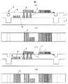
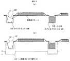
図1は光学式手段によりウェハ高さを検出する場合に発生する誤差を説明したものである。同図(a)は半導体ウェハの断面図である。半導体ウェハは光学的透明体である層間膜1により絶縁された微細な回路パターンが多層に積層されたものである。各層の回路パターンはコンタクトホール2により接続されている。光学式検査システムは、この微細回路パターン像を加工完了直後に撮像し、ショート、断線等の回路パターンの欠陥を検出して、製造工程の不具合を発見するものである。
【0019】
微細な欠陥を感度良く検出するためには、図に示す焦点深度3内に試料表面を保持して明瞭なパターン画像を撮像する必要がある。破線4は、焦点深度の中心軌跡であり、ウェハ表面を通過する理想的な状態を示している。この結果、同図(b)に示す様に最上層の回路パターン5が明瞭に撮像される。ここで、下層パターン6がデフォーカスして撮像されていないことに注意を要する。多層からなる半導体ウェハの検査においては、欠陥の発生工程、ひいては対策すべき不具合を有する製造工程を識別する必要がある。このためには、回路パターンが形成された直後に最表層のパターンに存在する欠陥のみを検出することが有利であり、下層パターンをデフォーカスさせることにより下層の欠陥が検出結果に混入することを防止できるのである。
【0020】
しかしながら、光学式手段によりウェハ表面高さを検出する場合においては同図(c)に示す様にウェハ表面が必ずしも安定して検出できない問題があった。この結果、同図(d)に示す様に像質の劣化(デフォーカス)を生じ、欠陥の見逃しや虚報の発生を引き起こしていた。半導体ウェハ表面を光学式手段により検出する場合、下記の誤差が問題となる。
【0021】
[透明膜で生じる誤差]
高さ検出に用いる照明光線が層間膜を透過し、下層で反射する。この結果、高さ検出値が下層の材質、形状に左右され不安定となる。例えば、本来検出すべき上層パターンでなく、下層パターンに焦点位置が一致する場合が発生し、上層と下層の区別がつかなくなる問題が生じる。
【0022】
[段差境界で生じる誤差]
段差境界では、上層と下層の平均的高さが検出される。この結果、上面および下面の両方がデフォーカスして検出されることとなる。また、段差境界7で実際には存在しない高さ(だまされ誤差)が誤検出される場合がある。この場合においても、検出画像がデフォーカスして検出される。
【0023】
[反射率が異なる境界で生じる誤差]
反射率が異なる境界において、実際には存在しない高さ(だまされ誤差)が検出される場合があり、検出画像がデフォーカスして検出される。
【0024】
本発明は、多様な材質からなり、かつ表面に起伏を有する半導体ウェハの様な試料の表面高さを安定に検出し、前記表面高さを用いて撮像状態を制御することにより、試料表面の高解像度な画像を安定して検出することを目的としている。
【0025】
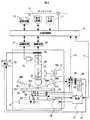
図2は本発明の第1の実施例である半導体ウェハの欠陥検査装置を示す。特に、本発明の好適な適用対象である、DUV光源の光学顕微鏡を応用した光学式パターン欠陥検査装置を例に説明する。
【0026】
[全体制御部]
全体制御部9は、装置全体の動作指示を司る。全体制御部9は、表示装置10を備え検査情報の表示等を行う。また、全体制御部9は、入力装置11を備え、ユーザ情報の取り込みを行う。さらに、全体制御部9は、記録装置12と接続されており、検査データ、レシピデータの管理を行う。また、全体制御部9は、外部ネットワーク13に接続されており、上位コンピュータや他の検査装置と検査データやレシピデータの送受信を行う。
【0027】
[撮像光学系]
キセノン光源14または水銀キセノン光源から発せられた光線が波長フィルタ15aにより帯域制限を受け、DUV(Deep Ultra Violet)光線が照明される。DUV光線としては、200〜400nmの様なブロードバンド照明であっても良いし、光源の輝線を選択しても良い。ブロードバンド照明では、ウェハの薄膜干渉による色むらを低減する効果がある。一方、輝線によるナローバンド照明では、光学系の色収差を精度良く補正できるため、解像度が向上する効果がある。
【0028】
PBS(偏光ビームスプリッタ)(15)においてS偏光が下方に反射し、λ/4板16を通過して円偏光となる。対物レンズ17によりウェハ18に照明された光線は、ウェハ表面で反射して、λ/4板16を再び通過することによりP偏光となりPBSを透過する。この構成により検出光量の激減が防止可能となる。反射光線は結像レンズ19により結像され、ウェハ表面の拡大光学像がリニアセンサ20上に形成される。このリニアセンサ20が撮像したウェハ表面の拡大光学像は、画像処理装置32に入力されて欠陥の検査が行なわれる。また、検出光路は分岐され、TVカメラ21が具備されている。TVカメラ21は画像処理装置22に接続され、アライメント、欠陥レビューに用いる。
【0029】
上記実施例では、DUV光源をランプ光源としたが、高輝度のレーザ光源を用いても良い。例えば、YAGレーザ(λ=532nm)と非線形光学素子を組み合わせて、第2高調波である266nmを用いることができる。
【0030】
[自動ステージ]
被検査対象であるウェハ18は、ウェハチャック23により真空吸着され、平坦化されると供に、ステージ移動時のずれを防止する。ウェハチャック23はZ、Θ、X、Yステージ30、24、25、26に搭載される。Θステージ24はウェハ搭載直後に実施されるアライメント時に制御され、整列して形成されたダイ配列をXステージ走査方向に一致させて、検査動作中は固定される。検査動作中は、Xステージ25が紙面に向かって左右に移動し、折り返し時にYステージ26が紙面に直交方向にステップ移動する。
【0031】
XYΘステージ24〜26はステージ制御コンピュータ27からの信号により制御される。Xステージ25の位置情報はレーザ測長器28により計測され、レーザ測長器28から出力される位置情報に基づきタイミング発生回路29により画素を示すスタートタイミング信号を発生し、リニアイメージセンサ20に送信されて、画像信号が読み出される。
【0032】
ステージ制御コンピュータ27は、全体制御部9とネットワーク13で接続されており、ダイレイアウト情報等をダウンロードして、検査位置の識別に用いられる。
【0033】
[撮像動作]
リニアイメージセンサ20は、スタートタイミング信号によりXステージが一定距離移動するたびに駆動される。リニアイメージセンサ20の読み出しを、Xステージ移動量に同期させることにより2次元画像が撮像できる。リニアイメージセンサ20として時間遅延積分型(TDI:Time Delay Integration)CCDセンサを用いることにより、高速走査においけるS/Nを向上できる。TDIセンサは複数の1次元イメージセンサを2次元に配列した構造を有し、各1次元イメージセンサの出力を定めた時間遅延しては対象の同一位置を撮像した隣接する1次元イメージセンサの出力と加算していくことにより、検出光量の増加を図ったものである。
【0034】
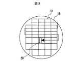
図3は、リニアイメージセンサ20によるウェハ18の表面の撮像動作の説明図である。同図の左右方向にXステージ25が一定速度で移動し、リニアイメージセンサ20により画像が撮像される。左右の折り返しではYステージ26が上下方向にステップ移動する。Yステージ26の移動量はダイピッチに一致しており、同図に示す様にリニアイメージセンサ20がX方向に移動する軌跡は、隣接ダイ間で同一位置となる様に制御される。なお、31は、ダイを示す。
【0035】
[画像処理]
リニアイメージセンサ20から出力されるアナログ信号は、A/D変換器(図示せず)によりデジタル信号に変換され、画像処理部32に入力される。図4により画像処理部32の動作を説明する。入力信号は2分岐され、一方が遅延回路33に入力される。すなわち、通過信号と遅延回路内の信号を遅延量だけずらして以降の処理を行う。遅延量はユーザが選択可能であり、ダイに形成された繰り返しパターンのピッチに一致させる。例えば、ダイ間比較の場合、ダイサイズを予め登録し遅延量とする。前記2種類の信号は位置ずれ検出回路34で画像間の位置ずれ量が算出され、一方の画像信号がシフト35される。差画像演算回路36において差画像が生成され、欠陥判定回路37において予め登録されたしきい値と比較され欠陥が検出される。欠陥部の画像信号からは特徴抽出回路38により、欠陥の座標、サイズ、形状、輝度情報等の欠陥情報が抽出され、検査終了後のグルーピングに利用される。前記欠陥情報は全体制御部9に送信され、データベース12に保存したり、表示装置10に表示したり、ネットワーク13を経由して上位コンピュータに転送される。
【0036】
[自動焦点システム]
自動焦点システムは、検出光学系47および自動焦点コンピュータ39からなる。検出光学系47は、撮像位置近傍の複数点の高さを検出し、自動焦点コンピュータ39に検出信号を送信する。自動焦点コンピュータ39は、図14に示すように、高さ計算回路106、制御量計算回路107等からなり、検出した高さと予め設定された制御目標との偏差に基づきZステージの制御量48を演算し、Zステージ30を制御する。自動焦点コンピュータ39は、ネットワーク13により全体制御部9と接続され、検査モード、レビューモードの様な動作モードの切り替え、および自動焦点用レシピの送受信が行われる。また、ステージ制御コンピュータ27からダイスタート信号40およびステージ折り返し信号41、タイミング発生回路29からTDIシフトパルス42が入力され、タイミング制御109に利用される。さらに検査中の自動焦点ON/OFF等、リアルタイム性の高い制御信号43がステージ制御コンピュータ27からDIOを経由して送信される。自動焦点コンピュータ29の詳細な動作は後ほど説明する。
【0037】
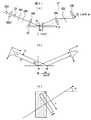
次に、本発明に係る自動焦点システムにおいて、特に特徴とするリニアイメージセンサ20による撮像範囲と上記検出光学系47による高さ検出位置との関係について図5を用いて説明する。撮像範囲44はリニアイメージセンサ20で一度に検出される範囲である。高さ検出手段(検出光学系)47は撮像位置近傍の複数点(45a〜45i)において、同図に示すように、走査方向46にWの幅を持つ範囲の平均的高さを検出する。本発明におけるより好ましい高さ検出手段47は、後ほど詳細に説明する。高さ検出位置(45a〜45i)は、撮像範囲44に対してステージ走査方向46に対称に配置された点を含むことを特徴とする。同図では、高さ検出位置(45a〜45i)は、撮像位置44に対してXステージ走査方向46にDだけずれて対称に配置されている。また、高さ検出位置(45a〜45i)は、ステージ走査方向46に直行する方向にも複数点で検出を行い、前記方向に段差が存在する場合の高さ検出に利用される。
【0038】
次に、上りの段差54における自動焦点動作について図6を用いて説明する。自動焦点動作は、自動焦点検出光学系47のセンサ205の検出動作、自動焦点コンピュータ39で実行される高さ計算、試料位置を制御する高さ制御の3ステップからなり、タイミング信号112に同期して動作周期Tで実行される。同図に示すように、センサ205の検出動作は、動作周期Tの期間で連続的に実行され、この信号に基づきTの期間を要して高さ計算が実行される。さらに、Tの期間を経て高さ制御が実行される。センサ205で検出される高さはTの期間に高さ検出位置を通過する試料の平均的な高さであり、T/2における試料高さが検出されると考えて良い。このため、センサの検出動作から高さ計算終了まではT/2+T、高さ計算終了から高さ制御終了まではTの遅れをもつ。
【0039】
破線50はセンサ205が検出する高さの軌跡、破線51は高さ計算結果の軌跡、実線52は実際の試料表面が制御された場合の焦点位置の軌跡を示す。ここで、高さ制御の応答性はZステージ30の性能に依存する。高さ計算結果の変動にZステージ30が追従できる場合は、実線52の傾きは破線51と一致する。しかし、高さ変動に対してZステージ30が追従できない場合は実線53となり遅れを生じる。
【0040】
この様に、焦点合わせを精度良く実施するためには、正確な高さ検出に加え、Zステージ30の応答性が重要である。このため、図2におけるZステージ30としては、リニアモータやボイスコイル等の高応答性能を有するアクチュエータが好適である。また、イナーシャの小さい対物レンズを上下に制御しても良い。
【0041】
さて、図2の様な、DUV光源を用いた高解像光学系では自動焦点システムの性能が特に重要となる。光学系の解像度RESと焦点深度DOFは次式(数1)及び(数2)で与えられる。
【0042】
RES=0.5×λ/NA ………(数1)
DOF=±0.5×λ/(NA2) ………(数2)
解像度を向上させるためにλを減少させると、λに比例して焦点深度が狭くなる。例えば、λ=266nm、NA=0.8とすると、DOF=±208nmとなる。一方、半導体ウェハに形成されるアルミ配線工程のパターン膜厚は500nmを超える場合があり、焦点深度を超える段差である。
【0043】
この様に、図1において説明した透明膜で生じる誤差、パターン段差で生じる誤差及び反射率が異なる境界で生じる誤差を低減し、ウェハ表面を前記焦点深度以内に制御することが課題となる。以下にこれらの誤差を低減する方法について説明する。
【0044】
まず、パターン段差で生じる誤差を低減する方法について説明する。以下、パターン段差を例に説明するが、パターン段差よりもさらに高さ変化が大きいダイ周辺のスクライブラインにおいても同様な効果が期待できる。
【0045】
図7は、段差境界部で発生するデフォーカスの様子を説明する図である。破線62は高さ検出値の軌跡であり、破線61は制御された焦点位置の軌跡である。図6で説明したように、段差境界では検出範囲の平均的な高さが検出されるため、検出値の軌跡は図(a)に示す様に検出範囲Wが段差にかかり始める位置から緩やかに上昇し、検出範囲全体が段差上面をカバーした地点で上面に一致する。下りの段差における軌跡も同様になだらかな軌跡となる。
【0046】
この結果、同図(a)に示す、上り段差と下り段差のデフォーカス範囲60においてパターン表面が焦点深度から外れ、図(b)の様にパターン63がデフォーカスして撮像される。この様なパターン境界のデフォーカスを低減する方法として、撮像位置に対して先行した高さ情報を用いて焦点合わせをする方法が、特開平7−86135号公報に記載されている。すなわち、図5において右方向にステージが移動する場合、撮像位置44より右側の高さ情報を用いて焦点合わせを行う。図7(c)に前記方式により制御される焦点位置の軌跡を破線65で示す。同図では上り段差では段差上面のデフォーカスが防止できているが、下り段差では63で示すように段差上面のデフォーカスが顕著となる。
【0047】
次に、本発明による第1の焦点合わせ方式について図8を用いて説明する。図8(a)は高さ検出値の軌跡である。同図の破線66の軌跡は、図5の走査方向にずれた3点(例えば45a、45d、45g)の高さに対応している。これら3点の検出高さから最大値を演算して代表高さとする。同図に示すように、高さ検出範囲Wにおいて高さが緩やかに変化するが、撮像位置44に対して前後Dはなれた位置の高さの最大値を採用することにより、上り段差および下り段差いずれにおいても、パターン表面の高さが正確に検出することができる。さらに、Xステージの走査方向によらず、上り段差および下り段差の高さ検出値の軌跡は対称である。この結果、図8(b)に示す様に段差上面に対して常に焦点合わせが可能となる。
【0048】
図8(c)〜(e)は段差境界付近にパターン欠陥が存在する試料を撮像した結果を、従来技術と本発明で比較したものである。同図(c)の破線67は従来技術による高さ検出値、破線68は焦点位置の軌跡である。上り段差に存在するショート欠陥69、下り段差に存在する断線欠陥70ともデフォーカスしてしまう。一方、同図(e)に示す本発明による焦点合わせ法により撮像した画像は同図(f)に示す様に、上り段差に存在するショート欠陥69、下り段差に存在する断線欠陥70とも明瞭に結像している。これらの画像を欠陥検査に応用すれば、段差境界に存在する欠陥を見逃すことなく検出可能となる。本第1の方式は、図8(e)に示す様にパターン段差前後にデフォーカス領域が存在し、ウェハ表面の凹凸に完全に追従しているわけではない。しかし、パターン上面に対しては常にフォーカスが合った状態にあることに注意されたい。半導体ウェハの様に、積層して製造される被検査対象物の最終工程の欠陥を検査する手段としては好適である。
【0049】
次に、検査速度の向上が目覚しい半導体ウェハ検査装置において本発明による第1の焦点合わせ方式を実施する方法について説明する。検査速度を向上するためには,Xステージの走査速度を向上させて撮像時間を短縮する必要がある。この様な状況において,パターン上面に対して常にフォーカスが合った状態とするためには,Zステージの追従性が問題となってくる。
【0050】
そこで,Zステージの制御方法を工夫して本第1の方式を実施する方法を図9(a)〜(d)により説明する。
【0051】
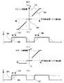
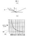
図9(a)は一般的なZステージ制御関数である。横軸は制御目標と高さ検出値の偏差であり,Zステージが制御目標に追従している場合ゼロ501,追従できていない場合大きな絶対値を有する。Zステージが制御目標に追従している場合とは,ウェハ表面が焦点深度内にあり明瞭な画像が撮像される状態である。縦軸はZステージ制御量である。同図では,横軸の偏差がゼロ付近の値ではZステージは移動させず,偏差が大きくなるにしたがって偏差に比例した制御量でZステージを移動させる。前記比例の係数(直線の傾き502)は制御ゲインであり,Zステージ駆動システムの安定性により1に対してどのくらいまで近づけられるか上限が決められる値である。
【0052】
偏差がある値より大きくなるとZステージの仕様で決められた最大ステップ量503づつ移動させる。同図の第1象限について説明すれば,制御目標に対して高さ検出値が大きな値を持つ場合であり,ウェハ表面が焦点位置に対して高い状態である。このため,Zステージを下方に駆動させる。このため,同図の横軸は右に行くほどウェハ高さが高い場合であり,縦軸は上に行くほどZステージを下方に駆動させることを意味している。
【0053】
図9(b)は段差を有するウェハにおける高さ検出値504と図9(a)の制御関数によりZステージが駆動された結果焦点位置が通過する軌跡505を重ねて表示したものである。Zステージの応答性が低い場合,段差上面を撮像中であっても焦点位置が段差上面に到達しないためデフォーカス506を生じる問題がある。そこで,本発明では図9(c)に示す制御関数によりZステージを制御する。同図では第3象限におけるZステージ駆動量が第1象限におけるZステージ駆動量に比べて小さい値に定義されていることに特徴がある。すなわち,Zステージを下方には従来どおりのシステムの最大ゲインで制御を行うが,上方には最大ゲインよりわざと少ないゲインで制御を行う。
【0054】
図9(d)は(b)に対応させて本発明による制御結果を表示したものである。最初の上り段差では従来と同様デフォーカス506が生じるが,下り段差では同図(c)の第3象限の効果によりZステージが上方にわずかしか移動しない。このため次の上り段差507ではすぐに上面パターンに焦点位置を追従させることができ,上り段差で生じるデフォーカスの発生を防止できる。
【0055】
次に、本発明による第2の焦点合わせ方式について図10を用いて説明する。本第2の方式は、パターンの下面である層間絶縁膜上に存在する欠陥を検出する場合に好適である。層間絶縁膜ではCMP(Chemical Mechanical Polishing)による平坦化が行われる際にスクラッチ欠陥74、75が発生する。スクラッチ74、75はパターンのショート、断線を発生させる致命的な欠陥である。図10(a)は高さ検出値の軌跡である。同図の破線の軌跡は、図5に示す走査方向46(X)にずれた3点(例えば45a、45d、45g)の高さに対応している。
これら3点の検出高さから最小値を演算して代表高さとする。この結果、パターンが存在しない段差下面に対して常に焦点合わせが可能となる。
【0056】
図10(c)〜(e)は段差境界付近の層間絶縁膜表面に存在するスクラッチ欠陥を撮像した結果を、従来技術と本発明で比較したものである。同図(c)の破線72は従来技術による高さ検出値、破線73は焦点位置の軌跡である。上り段差直前や、下り段差直後に存在するスクラッチ欠陥74がデフォーカスしてしまう。一方、同図(e)に示す本発明による焦点合わせ法により撮像した画像は同図(f)に示す様に、これらの欠陥74、75が明瞭に撮像される。これらの画像を欠陥検査に応用すれば、段差境界に存在する欠陥を見逃すことなく検出可能となる。
【0057】
次に、本発明による第3の焦点合わせ方式について図11を用いて説明する。本第3の方式は、パターンをエッチングした底に存在する欠陥80を検出する場合に好適な方式である。エッチング工程では、パターンとパターンの間の谷底にエッチング残り80が発生し、パターンショートを引き起こす致命欠陥となる。こうした致命欠陥はパターンが形成されている全域で検出する必要がある。
【0058】
図11(a)は高さ検出値の軌跡である。同図の破線の軌跡は、図5に示す走査方向46(X)にずれた3点(例えば45a、45d、45g)の高さに対応している。図8と同様にこれら3点の検出高さから最大値を演算し、更にパターン段差の高さだけ下方にオフセットを減算して代表高さとする。この結果、パターンが形成されている領域において常にパターン谷底に焦点合わせが可能となる。
【0059】
図11(c)〜(e)はパターンとパターンの間の谷底に存在するエッチング残り80を撮像した結果を、従来技術と本発明で比較したものである。同図(c)の破線78は従来技術による高さ検出値、破線77は焦点位置の軌跡である。上り段差直後に存在するエッチング残り欠陥80がデフォーカスしてしまう。一方、同図(e)に示す本発明による焦点合わせ法により撮像した画像は同図(f)に示す様に、これらの欠陥80が明瞭に撮像される。これらの画像を欠陥検査に応用すれば、段差境界に存在する欠陥を見逃すことなく検出可能となる。
【0060】
以上、図8から図11に述べた本発明による実施例においては、着目工程の段差境界付近の欠陥69、70、74、75、80を明瞭に検出できる特徴がある。
【0061】
次に、全体制御部9が自動焦点コンピュータ39に対して行う上記実施例における焦点合わせに関する条件設定画面について図12を用いて説明する。図12(a)において、表示装置10に表示された焦点合わせに関する条件設定画面において、ユーザが編集したい品種、工程名称301、302を指定すると、関連データが読み込まれ、品種、工程名称が表示される。次に、ユーザは画面メニュー(自動検査303、欠陥確認304、条件出し(レイアウト設計305a、自動焦点設定305b、しきい値設定305cからなる)305)を選択する。同図では条件出し画面310が選択され、更にサブ画面である自動焦点設定305bの高さ演算ルール305baが選択中となる。
【0062】
高さ演算ルール305baは、図8から図11で説明した撮像位置近傍の複数の高さ検出値から代表高さを演算するルールである。パターン表層の欠陥を見逃すことなく検査したい場合は図8で説明した様に最大値を、パターン下層の検査を正確に行いたい場合は最小値を選択する。この他、CMP後の様な平坦で段差が無いことが予め判っている工程においては、平均値を選択することにより、複数点の高さ検出結果が平均されて安定な表面高さ検出が可能となる。この他高さ演算ルール305baはユーザが定義可能である。
【0063】
図12(a)に示す画面310にはウェハマップ(100)とウェハ内の着目ダイの拡大図(101)が表示されている。図12(b)は焦点合わせに関する条件設定画面の別の例である。同図(b)は、被検査工程において、どの高さ演算ルール305baが最も安定に欠陥検査が可能かを比較できる画面の例である。同図の左側は複数点の高さの最大値を選択して撮像した検査した特定ダイの欠陥マップ(101a)である。同図に示す様に、レイアウトデータ(102)が重ね表示されており、欠陥が存在するパターンの種類を識別する指針となる。
【0064】
レイアウトは、機能や形成工程が異なるパターンがブロック表示さてたものであり、CADデータを参照して表示される。右側は高さ演算ルール305baを変えて検査した前記と同一ダイの欠陥マップ(101b)である。異なる高さ演算ルールの欠陥マップを比較することにより、当該工程に適切な高さ演算ルール305baが選択可能となる。図12(b)では、複数点の高さの平均値(101b)に比べ、最大値(101a)の方がパターン領域境界近傍の欠陥検出感度が良いことが判る。演算ルールの代わりにオフセットを変更して欠陥マップを比較しても良い。適切な高さ演算ルール305baが選択されると登録ボタンを押してレシピに登録する。
【0065】
次に、本発明による第4の焦点合わせ方式で用いるフォーカスマップ330について図13を用いて説明する。このフォーカスマップ330は、自動焦点コンピュータ39および主制御部9のどちらで作成してもよい。フォーカスマップ330はダイ内を走査して検出される高さをX、Yの2次元テーブルに対応させ
て記録したデータであり、(X,Y,Z)のデータ列からなる。
【0066】
図13(a)に示すパターンを走査したとき検出されたフォーカスマップ330を鳥瞰図として示すと同図(b)の様になる。同図(c)はフォーカスマップの作成手順である。フォーカスマップ330は同一ダイを左方向スキャンしたデータと、右方向スキャンしたデータを取得し、両者の結果を演算して作成する。なぜなら、左方向と右方向では、段差境界における高さ検出値またはウェハ表面の軌跡が異なるためである。なお、左方向スキャンと右方向スキャンのデータを内部メモリ108等に別に登録し、それぞれのスキャン方向に応じて選択的に読み出して利用しても良い。
【0067】
同図の破線(103)は高さ検出値の軌跡であり、破線(104)はウェハ表面の軌跡である。実線(105)はこれらスキャン方向が異なる軌跡データを同一座標ごとに重ね合わせ両者の最大値を演算した結果である。軌跡データとしては高さ検出値の軌跡(103)およびウェハ表面の軌跡(104)をそれぞれ別に演算する。前記演算結果を2次元データとして例えば高さ記録メモリ108に記録して、フォーカスマップ330として利用する。フォーカスマップの有用性は以降で詳細に述べる。
【0068】
次に、本発明に関係する自動焦点コンピュータ39について図14を用いて説明する。図14は、本発明に係る自動焦点コンピュータ39の一実施例を示すブロック図である。自動焦点コンピュータ39は高さ計算回路106、制御量計算回路107、高さ記録メモリ108、タイミング制御回路109からなる。フォーカスマップを作成する場合、特定ダイをXステージ25で走査しながら、高さ計算回路106で計算される同一地点の高さ計算結果および制御量計算回路107で計算されるZステージ移動量を、タイミング制御回路109から得られる動作周期ごと、または複数の動作周期ごとに高さ記録メモリ108に記録する。
【0069】
タイミング制御回路109にはステージ制御コンピュータ27からダイスタート信号40が、タイミング発生回路29からTDIシフトパルス42が送信される。タイミング制御回路109は、ダイスタート信号40を起点としてTDIシフトパルス42をカウントし、制御タイミング信号112を生成する。この信号112を高さ計算回路106、制御量計算回路107、高さ記録メモリ108に入力し、信号に同期させる。この結果、ダイ内で高さ計算、Zステージ制御、Zステージ位置の読み出しを同一位置で実施できる。
【0070】
高さ計算回路106から出力される信号は図6(b)の破線51aであり、制御量計算回路107の出力は図6(b)の実線52である。両者を加算することにより、図6(a)の破線のウェハ段差プロファイルデータ51となる。制御量計算回路107の出力の代わりに、Zステージポジション(113)を読み込んで代用しても良い。記録したフォーカスマップ330はネットワーク(13)により全体制御部9に転送され、レシピデータとして、品種・工程別に管理される。
【0071】
フォーカスマップ330を利用する場合、全体制御部9からダウンロードして高さ記録メモリ108に記録する。そして、位置情報に基づき該当する位置のフォーカスマップ330を読み出し、高さ計算結果と比較して、Z制御量を計算する。計算された制御量に基づきZステージ30に制御信号48を送信する。制御量計算回路107にはステージ制御コンピュータ27から折り返しダイ識別フラグ114、スキャン方向識別フラグ114bが入力される。タイミング信号112に同期してフォーカスマップの読み出し、高さ計算、制御量計算、Zステージポジション読み出しを行うことにより、比較検査を行うダイ同士の撮像状態を一致させることができる。
【0072】
次に、本発明による第4の焦点合わせ方式について図15を用いて説明する。本第4の方式は、ダイ内のパターンの凹凸によらず、予め設定した任意の高さを保持した状態でパターン像が撮像できる。このため、着目したパターンに存在する特定の欠陥を選択的に検出できる。
【0073】
図15(a)はフォーカスマップに記録された高さ検出値の軌跡である。同図(b)は着目したパターンの検出高さが定義された様子を示す。同図の場合、パターン上面位置(115)をダイ全面において検出することを示している。同図(c)は同図(b)から算出したオフセットマップである。同図(b)の高さをダイ全面で検出するためには、高さ検出位置(X,Y)においてオフセットを変更する必要がある。このため、同図(c)のオフセットを例えば自動焦点コンピュータ39において予め算出しておく。前記オフセットマップはフォーカスマップと同様に図13に示す高さ記録メモリ108に記録される。
【0074】
同図(d)は同図(c)のオフセットマップを用いて検出した高さ検出結果である。高さ検出結果(116)に同図(c)のオフセットを加算して検出高さとして試料表面位置を制御したものである。Zステージ30の動作遅れの影響を除外するためには、同図(a)において高さ検出値の軌跡ではなく、焦点位置の軌跡を用いる。
【0075】
次に、本発明に係る欠陥検査装置における全体制御部9または自動焦点コンピュータ39において、フォーカスマップ330を用いた検査レシピの設定について図16を用いて説明する。図16は、表示装置10におけるフォーカスマップ330を用いた検査レシピの設定画面320である。図16(a)各ボタンの役割は、図12で説明した。画面にはダイ内のレイアウト102とフォーカスマップ117が2次元画像として表示される。
【0076】
フォーカスマップ117は2次元の濃淡画像として表示されている。濃淡の階調は高さに対応している。ユーザはレイアウトまたはフォーカスマップに表示されるカーソル118により、特定パターンブロックや焦点合わせすべき高さを選択できる。カーソルはレイアウト、フォーカスマップ、階調表示部で連動している。焦点合わせすべき高さを選択して登録ボタンを押すことにより、表示されている品種、工程名称のレシピに登録される。同図のレイアウトのハッチング部119が選択された高さを検査した場合に選択的に焦点合わせされて欠陥が検出されるパターンを示している。
【0077】
同図(b)は検査レシピ設定画面の別の実施例である。カーソルで選択された位置120の1スキャン分のプロファイルデータ121が表示される。同図(c)はフォーカスマップ330が鳥瞰図として3次元表示されている。フォーカスマップ330を3次元表示することにより、焦点合わせすべき高さが明瞭に識別できる。
【0078】
次に、前述した本発明による第4の焦点合わせ方式の効果について図17を用いて説明する。図17(a)〜(c)は複数の欠陥が存在するパターンを撮像した結果を、従来技術と本発明で比較したものである。破線122(116)は高さ検出結果、破線123は本第4の焦点合わせ方式により制御される焦点位置の軌跡である。焦点位置が破線122の軌跡を移動する場合、パターン表面に存在する断線70、ショート69のみならず、層間絶縁膜表面に存在するスクラッチ欠陥75も撮像される。
【0079】
一方、本実施例によれば、パターン表面のみに焦点合わせが行われるため、パターン表面に存在する欠陥のみが明瞭に撮像され、下面に存在するスクラッチ欠陥75はデフォーカスしている。この方式を欠陥検査装置に応用すれば、着目パターンに存在する欠陥が選択的に検出でき、欠陥検出結果の発生工程識別が容易となり、不良工程の発見・対策が迅速化できる。
【0080】
次に、試料上に繰り返し形成されたパターン同士を比較して欠陥を検出する欠陥検査装置において、比較するパターン同士の撮像状態を一致させることにより、微細な欠陥を感度良く検出できる方法について説明する。比較検査においては、比較するダイ間で同様に焦点合わせ誤差が発生していれば、不一致を生じない。しかし、一方のダイのみで焦点合わせ誤差が発生すれば、不一致を生じて虚報となる。このため、比較するダイ間で焦点合わせ状態が一致するような構成とする必要がある。
【0081】
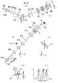
次に、本発明に係る自動焦点コンピュータ39が、焦点合わせをダイ間の同一位置で実行する実施例およびその効果について図18を用いて説明する。
【0082】
まず、図18(a)〜(d)により焦点合わせがダイ間の同一位置で実行されない場合を説明する。同図(a)は焦点合わせの軌跡を示し、同図(b)は動作タイミング信号である。同図(b)の信号は、例えば、自動焦点コンピュータ内部で生成されたXステージ位置とは無関係な信号であり、この信号に同期して高さ検出、Zステージ制御が実行される。また、(a)の矢印は比較検査で比較されるダイ間で同一な位置を示している。パターンの開始点(124)に着目すると、左と右のダイでは、パターン開始位置と高さ検出タイミングが一致していない。このため、同図(c)に示す検出画像で左側のダイではパターンがフォーカスしているのに対して、右側のダイではデフォーカスしている。パターン終点(125)においても同様に左右のダイの焦点合わせ状態が一致していない。この結果(d)の差画像は、焦点合わせ状態が一致しない、パターンの始点と終点で不一致を生じ、虚報の原因となる。
【0083】
次に、本発明のように、図18(e)〜(i)により焦点合わせがダイ間の同一位置で実行される場合を説明する。同図(e)は同図(a)に対応する焦点合わせの軌跡を示し、同図(g)は高さ検出手段47の動作タイミングである。また、同図(f)はXステージ位置から判定されるダイスタート信号40である。本実施例では、同図(g)に示すパルス42が(f)のダイスタート信号40に同期している点に特徴がある。この結果、左と右のダイで、パターン開始位置と高さ検出タイミングを一致させることができ、同図(h)に示す様にパターンの始点や終点の焦点合わせの状態を一致して撮像できる。このため、同図(i)に示す様に差画像350において不一致を生じることがなくなる。
【0084】
次に、本発明に係る自動焦点コンピュータ39が、ステージ折り返しで比較するダイ間の高さ検出値を一致させる対策の実施例について図19を用いて説明する。図19(a)に示す折り返し位置では、上下のダイ画像126を比較する必要がある。このとき、上側のダイと下側のダイではステージ移動方向が逆向きであり、方向に依存する高さ検出誤差が発生し不一致を生じる。しかし、図6で説明した様に、ステージの応答性能が低い場合、高さ検出値と焦点位置の軌跡は一致しないため、前記折り返し部での誤差が発生する。
【0085】
このために、本実施例ではフォーカスマップ330を利用して、走査方向が逆向きであってもダイ同士の表面高さの軌跡を一致させる。図19(b)の破線127は左から右に走査した場合の焦点位置の軌跡であり、実線128は右から左に走査した場合の焦点位置の軌跡である。これら2つの軌跡は段差境界で一致せず、比較検査による虚報発生の原因となる。
【0086】
そこで、本実施例では、同図(b)の破線129がフォーカスマップ330の軌跡であるから、高さ検出値とフォーカスマップ330の差分がしきい値を超える位置では、フォーカスマップ330を高さ検出値として代用し、焦点位置の制御を行う。この結果、左から右に走査する軌跡を破線130で示す軌跡で制御可能となり、比較検査の虚報発生を低減することができる。
【0087】
従来技術は、図19(c)〜(g)に示すように、段差境界部で焦点合わせの状態が異なるため虚報が発生することになる。(c)は右方向走査の軌跡、(d)は(c)の軌跡において撮像した画像、(e)は左方向走査の軌跡、(f)は(e)の軌跡において撮像した画像、(g)は(d)と(f)の差画像である。本発明の場合には、図19(h)〜(l)に示すように、(h)と(j)の軌跡が一致するため(i)と(k)の撮像条件がほぼ等しく、(l)で虚報の発生が防止できる。(h)〜(l)は(c)〜(g)に対応する本発明の実施例である。
【0088】
次に、本発明に係る自動焦点コンピュータ39が、ダイ周期とは異なる露光ショット周期で高さ変化が大きいパターンが形成されたダイ周辺のスクライブラインを走査する場合であっても、比較するダイ間の高さ検出値を一致させる実施例について図20を用いて説明する。
【0089】
図20(a)はダイ周期とは異なる露光ショット周期で高さ変化が大きいパターンが形成されたダイ周辺のスクライブラインを走査する場合の問題点を説明した図である。スクライブラインA508にはないパターン510がスクライブラインB509に形成されているとする。
【0090】
スクライブラインA508ではZステージ30は高さ検出値131に追従しようとして上昇するため,焦点位置の軌跡132が同図の様に下降し,上り段差でZステージ30が最大速度で下降しても,焦点位置の軌跡132がパターン表面に一致するまでに距離を要する。一方,スクライブラインB509ではパターン510が形成されているため,焦点位置の軌跡が異なる。この結果,スクライブラインAの直後およびスクライブラインBの直後で検出された画像同士を比較すると不一致を生じ虚報となる。
【0091】
そこで、図20(b)に示すように、本発明によるステージ制御の切り替えを行う。同図(b)にはステージ制御ON/OFF信号を併記している。ステージ制御ON/OFF信号511は,現在位置をステージ制御コンピュータ27が識別しDIO信号43を通じてZステージ30に送られる。画像比較を行う領域ではON(同図のH,Hは信号がHighの状態にあることを意味する),画像比較を行わない領域ではOFF(同図のL,Lは信号がLowの状態にあることを意味する)が出力される。
【0092】
この結果,段差変化が大きなスクライブラインではステージ制御がOFFとなるため高さ変化が大きな段差に追従せず,画像比較を行う領域では常に焦点位置の軌跡132をパターン表面に追従させることができる。上記実施例ではスクライブラインを例に本発明の効果を説明したが,ステージ加速・減速時のチャックの浮き上がり,ウェハ外を走査する場合に発生する誤差,についても上記と同様な効果が得られ,画像比較を行う領域における焦点合わせ状態を一致させることができる。
【0093】
以上、パターン段差で生じる誤差を低減する方法について説明したが、前記実施例は高さ検出手段47がウェハ表面位置を正確に検出できることが前提であった。しかし、図1で説明した様に、ウェハ表面に存在する急峻なパターン段差、反射率分布、光学的透明体等が高さ検出誤差の原因となる。
【0094】
そこで、次に、本発明に係る上記要因による誤差の影響を受けることなく試料表面の高さ検出が可能な高さ検出方式について説明する。
【0095】
図21には、本発明にかかわる高さ検出方式の構成を示す。試料18の斜め上方から入射角度Θで照明する光線により、スリット202をウェハ試料面上に結像させる。そして、ウェハ上のスリット像をセンサ205上に結像させる。試料18がZ移動した場合、スリット像は試料上でZ・tanΘ移動し、センサ205上では2Z・sinΘ・m移動する。ここで、mは光学系の倍率である。スリットの幅をdとすれば、試料上の投影範囲はd/cosΘとなり、この投影範囲において平均的高さが検出される。
【0096】
さらに、好ましい構成としては、Θとしては、80度以上、より好ましくは85度以上とする。また、光路中に偏光素子203bを挿入し、S偏光を抽出する。また、スリット202はステージ移動方向46(X)に対してψ度回転して投影する。また、コンデンサレンズ201の焦点位置にスリット202を配置し、ケーラ照明としてスリット202の明るさを均一化する。また、照明光路にはレンズ204の後側焦点位置に絞り203を設け、テレセントリック照明として試料18が上下に移動した場合にスリット像の大きさが変化しにくい構成とする。
【0097】
また、検出レンズ204の前側焦点位置にもスリット203を設ければ、試料18で回折した高さ検出のノイズ要因となる回折光線を除去できる。
【0098】
上記構成の有効性は以下の説明により明らかにされる。まず、上記構成が光学的透明体の高さ検出誤差を防止する効果について説明する。
【0099】
図22は層間絶縁膜の様な光学透明体で生じる高さ検出誤差を説明したものである。同図(a)は斜め方向から入射された照明光線が透明体で透過または反射する様子を説明したものである。照明光線は透明膜の上面で反射光と透過光に分岐される。透過光線は透明膜下面で反射し、さらに上面で透過光と反射光に分岐される。透明膜の透過光は平行光線となりセンサ205に入射する。ここで、下面で反射した光線はセンサ上で下方にずれて検出される。このため、検出される光線の位置は下方にずれたものとなり、見かけ上試料位置が下方にずれたものとみなされてしまう。
【0100】
同図(b)は照明光線の入射角度と反射率の関係を偏光方向別に示している。同図に示す様に反射率を50%以上とするためには、S偏光210で80度以上とする必要がある。同図(c)は照明光線の入射角度と同図(a)で説明した高さ検出誤差の関係を示したものである。透明膜の膜厚を1.0μm、下面の反射率を1.0としている。この場合、高さ検出誤差をDUV光学系の焦点深度である200nm以下とするためには、S偏光210で85度以上とする必要があることがわかる。このため、図20で説明した構成においては、入射角度を80度以上、より好ましくは85度以上とし、S偏光を抽出している。
【0101】
次に、光学的透明体の表面高さを精度良く検出するとともに、反射率分布の影響を低減する方法を説明する。
【0102】
図23は図21の構成において反射率が異なる境界において誤差が発生する様子を説明している。同図(a)は右側が低反射率部材、左側が高反射率部材で構成された領域にスリット202が投影された様子を示している。スリット波形は反射率が異なる境界で反射し、同図に示す様な歪んだ波形211となる。この結果、本来検出されるべき破線で示した位置212から上方にずれた位置をスリット位置213として検出してしまう。この結果、みかけ上、上方向にずれた位置が検出されたものとなる。前記誤差を低減するために、同図(b)〜(d)の対策をこうじる。
【0103】
同図(b)はスリット202をステージ移動方向214に対してψ度回転して投影した場合を示している。ウェハに形成されるパターンはステージ走査方向に対して平行または直交して形成されることが多い。同図にスリット投影領域が、反射率が異なる境界を左右にまたぐ事例を示している。同図左に示すスリット投影像202aが回転しない場合は波形が歪み、誤差を生じる。一方、スリット投影像202aを回転させることにより、投影領域の反射率分布がスリット長手方向に平均化される。同図の場合、理論的な誤差をゼロとできる。
【0104】
一方、図23(c)または(d)は誤差低減の別の対策例である。同図(c)または(d)の左図はスリット投影領域が、反射率が異なる境界をまたいで投影された場合の波形の例である。同図(c)の左図は右側に低反射率部があり歪んだ波形となっている。同図(c)中央図は同波形の重心を演算してスリット位置を検出した事例である。この場合、波形の歪みが顕著な波形ピーク位置の上方の重みが大きく、重心位置215は左側にシフトする。右図は本発明によるスリット位置検出の1実施例である。予め設定したしきい値217と波形の交点216を求め、交点の中央218をスリット位置とする。しきい値を最大値の50%以下、より好ましくは10%程度に設定することにより、反射率の違いによる波形歪みの影響を受けにくくできる。
【0105】
同図(d)は他の実施例である。左図は同図(c)の左図と同一である。中央図は次式(数3)の波形である。
【0106】
I2=log(I1+1) ………(数3)
同図に示す様に、低レベルの波形のゲインを大きく、高レベルの波形のゲインは小さくなる。この変換を実施することにより、右図の様に高レベルの波形がつぶれた波形となる。この結果、高レベルで顕著である波形歪みの影響を低減できる。以上説明した図23(b)および(c)または(d)を同時に実施することにより、反射率の違いに起因する誤差をより低減できることは言うまでもない。
【0107】
次に、光学的透明体の表面高さを精度良く検出するとともに、段差境界で高さ検出誤差の発生を防止する方法について説明する。図25は図21の構成における照明光線が段差境界部を照明した場合を示している。まず、同図(b)により下り段差(221)において誤差が発生する原理を説明する。同図(b)はスリット光が段差上面から下面に移動した場合を示している。左図が段差上面を照明した場合である。本来、破線で示す位置(222)が段差上面を正しく検出する位置である。しかし、照明光は段差部で2本に分離されてセンサ205に到達する。段差下面からの反射光(223)は上面からの反射光(224)に比べて光量が少なく、コントラストが低下した状態で検出される。このため、高さ検出値は上面からの反射光に基づき検出される。このため、みかけ上段差上面の検出値(225)が上側にシフトする。また、スリット光が右方向に移動した右図の場合には段差下面からの反射光(226)が検出されるため、みかけ上段差下面の検出値は下側にシフトする。この結果、図25(a)の様な実際には存在しない高さの軌跡(227)となる。
【0108】
次に、図25(c)により上り段差(229)において誤差が発生する原理を説明する。同図(c)はスリット光が段差下面から上面に移動した場合を示している。左図が段差下面を照明した場合である。同図に示すように、下面の光線は遮光されて上面からの反射光のみが検出される。したがって、みかけ段差下面の検出値が上側にシフトする。また、スリット光が右方向に移動した右図の場合には段差上面からの反射光のみが検出されるため、みかけ上段差下面の検出値は下側にシフトする。この結果、図25(a)の様な実際には存在しない高さの軌跡(228)となる。
【0109】
次に、本発明に係る段差部の誤差を低減するための実施例について図26を用いて説明する。本発明では、図21(c)に示す様に段差境界が存在する方向に対してψ度回転してスリット202を照明する。そして図26(b)に示す様にスリット長手方向の範囲Lのスリット光を積分して検出する。図26(b)は下り段差(221)でスリット光が分離される場合を示しているが、図25(b)の様に検出波形(230)が分離して検出されることを防止できる。同様に図26(c)は上り段差(229)でスリット光が遮光される場合を示しているが、遮光されない領域が積分範囲Lに含まれるため遮光によりスリット光がシフトする影響を低減できる。前記実施例により段差境界高さを検出した軌跡を図26(a)に示す。検出値(231)は段差上面と下面の間の平均的な値に収まる。このような効果は積分範囲Lが長いほど顕著となる。以上、図22から25により図21の構成の有効性を説明した。
【0110】
次に、本発明に係る図21に示す構成において、図5に示す撮像範囲44近傍の複数点(45a〜45i)の高さを検出する構成の第1の実施例について図26を用いて説明する。
【0111】
図27(a)は図21(a)の受光センサを分割センサ(232)としたことに特徴がある。図27(a)は横方向から、図27(b)は上面から見た図である。図27(c)は図2の構成に適用した場合にリニアセンサ撮像位置(44)と高さ検出位置の関係を示している。図27(d)〜(f)は分割センサ(232)の実施例である。図27(a)〜(f)の座標系(試料面のXYZとセンサ面のY'Z')は共通である。
【0112】
図27(d)はPSDをY'方向に並べたものであり、試料面からセンサ面を見込んだ場合を示す。Y'方向の各位置においてスリットのZ'方向へのシフト量を算出することにより、試料面の複数点の高さを検出できる。スリットが、Z'の正の方向にシフトすると試料がZ方向に下がった場合を意味する。PSDのA〜Eは図27(c)の検出位置A〜Eに対応する。同図(c)の配置は図5の実施例であり、撮像領域44に対してステージ走査方向46に等間隔だけずれた複数点が検出可能である。また、撮像領域44の長手方向に対しても複数点が検出される。従って、自動焦点コンピュータ39において、同図(c)で検出されたA〜Eの高さから最大値や最小値を演算することにより、図8〜図11で説明した高さ検出方式が実現できる。
【0113】
図27(e)は、分割センサとして2分割ホトダイオードをY'方向に並列に並べたものであり、同図(d)と同様な機能を実現できる。さらに図27(f)は分割センサとして2次元CCDセンサを用いた実施例である。Y'方向の各画素位置においてスリットのZ'方向へのシフト量を算出することにより、試料面高さ分布を詳細に検出できる。また、Z'方向のスリット波形に対して図23(c)(d)の波形処理を実現できる。
【0114】
次に、本発明に係る図21に示す構成において、図5に示す撮像範囲44近傍の複数点(45a〜45i)の高さを検出する構成の第2の実施例について図27を用いて説明する。図28は高速な1次元ラインセンサを用いて図27(f)の様な複数点の波形処理機能を実現するものである。図28は、図21の検出光路に機能を付加したものである。図28(a)は横方向から、同図(b)は上面から見た様子である。試料18からの反射光は検出レンズ204により拡大検出される。検出レンズ204の後側焦点位置に絞り203が配置され、試料18からの散乱光を遮光する。シリンドリカルレンズ233は前記検出レンズ204の後側焦点位置に、前側焦点位置を一致させて配置されており、検出光線をコリメートする働きがある。コリメート光線はスリット長手方向に角度をずらして配置された平行シフトプリズム234によりシフトされる。
【0115】
図28(d)は平行シフトプリズム234の原理図である。平行板ガラスに入射角度Θで入射された光線は次式(数6)の距離δシフトする。
【0116】
δ=(1−1/N・cosΘ/cosΘ')d・sinΘ ……(数6)
ここで、Nはガラスの屈折率、dはガラス板の厚み、Θ'はガラス板で屈折された光線が入射面の法線となす角度である。
【0117】
図28(a)では3枚の平行シフトプリズム234により、スリット長手方向を3分割して、スリット両端の光線を平行シフトさせた様子を示す。シリンドリカルレンズ235の後側焦点位置に、1次元ラインセンサ236が配置されており、3分岐されたスリット光線が1次元ラインセンサの離れた位置において画素幅に結像される。図28(c)は図2の構成に本実施例を適用した場合のリニアセンサ撮像範囲44と高さ検出位置の関係を示している。同図(c)のA、B、Cは図28(a)(b)(e)のA〜Cに対応している。同図(e)はラインセンサ236で検出されるスリット波形である。スリットが、Z'の正の方向にシフトすると試料が下がった場合に対応する。原点に対してA〜Cのおのおのの波形位置求めることにより各位置の試料高さが求まる。
【0118】
図28(c)の配置は図5の実施例に対応し、撮像領域44に対してステージ走査方向46に等間隔だけずれた複数点が検出可能である。また、撮像領域44の長手方向に対しても複数点が検出される。従って、自動焦点コンピュータ39において、同図(c)で検出されたA〜Cの高さを比較演算することにより、図8〜図11で説明した高さ検出方式が実現できる。
【0119】
図29は図27の構成を2式設けた構成である。(a)は上面図であり、(b)は図2の構成に本実施例を適用した場合のリニアセンサ撮像領域44と高さ検出位置の関係を示している。図29(b)の配置は図5の実施例である。図27(c)の片側の場合に比べ、リニアセンサ長手方向に非対称な段差やパターンにおける高さ検出が正確に求まる特徴がある。
【0120】
以上、図21〜図29によりウェハ表面に存在する急峻なパターン段差、反射率分布、光学的透明体等に対して表面高さを正確に検出する高さ検出方式について説明した。
【0121】
なお、上記図21の構成は、撮像光学系とは別光路による高さ検出手段であるため、環境変化、特に温度変化による撮像光学系の焦点位置に対する高さ検出光学系の原点ドリフトを安定化させる必要がある。図30は原点ドリフトを説明したものである。同図(a)は図21の高さ検出光学系を図2の構成に実装する1形態である。スリット205を2枚のアクロマートレンズ291で試料位置に結像し、反射光を2枚のアクロマートレンズ291で中間象を結像し、対物レンズ200により拡大して感度を確保する構成である。照明光源および対物レンズ200以降の光路は省略し、環境変化に敏感な範囲のみが記載されている。高さ検出光学系47の各部品はベース部材295に固定されている。
【0122】
同図(b)は初期状態である同図(a)に対して温度上昇して、対物レンズ17の鏡筒296、高さ検出光学系のベース部材295が熱膨張した様子を示している。同図(c)は(b)の先端部を拡大表示したものである。初期状態では実線で示す様に高さ検出光学系の結像位置と撮像光学系の焦点位置が一致していたものが、温度上昇に伴いそれぞれ異なる位置に変位している。この結果、高さ検出系の原点に対する撮像系の焦点位置が変化するため、欠陥検査装置に登録されている自動焦点オフセット値(レシピ)が使用できなくなる。
【0123】
この様な環境変動の影響を補正する方法を説明する。これにより、環境変動の影響を受けることなく過去のレシピを活用したり、異なる装置間でレシピを共有化することができる。
【0124】
次に、キャリブレーション方法について図31を用いて説明する。キャリブレーションでは、図2のウェハチャック23に搭載されている標準試料片453、454を用いる。図2には2種類の試料片453、454が搭載されている。1方453はパターンが形成されていないミラーであり、シェーディング補正に使用する。他方454は微細なパターンが形成されているものであり、図31で説明するキャリブレーションに使用する。キャリブレーションは検査前に実施する。また、検査装置に搭載された温度モニタの値があらかじめ決められたしきい値を上回る場合に実施する。更に、時間により実施頻度を決めても良い。
【0125】
同図(a)はキャリブレーションのフローチャートである。まず、XYステージ25、26を移動させて標準試料片454の位置を光軸に位置させる(S31)。
【0126】
次に標準試料454を引き込み範囲内に移動させる(S32)。この手順を(b)に示す。まずZステージを最下位に移動させ(S321)、次に予め決められた一定量のステップずつ上方向に移動する(S322)。自動焦点コンピュータ39は受光センサに光線が入射したか否かを判定することにより、検出範囲内か否かを判定する(S323)。否の場合には、S322に戻ることになる。
【0127】
検出範囲内であると判定されるとAF−ON(S324)となり、(a)の次のステップ(S33)に進む。Zステージを一定量移動させた状態(S33)で、自動焦点コンピュータ39により高さ検出を行い(S34)、検出結果を全体制御部9に転送する。次にTVカメラ21により画像を検出し(S35)、検出された画像から画像処理部22においてコントラスト値を演算する(S36)。コントラスト値としては、画像内の決められた領域の範囲の分散値の様な値である。
以上の手順を予め決められたステップ数繰り返すことにより(S36)、画像処理部22または全体制御部9において、同図(c)の波形が得られる。同図の横軸は試料高さであり、縦軸はコントラスト値である。同波形を多項式、例えば2次関数により近似してピーク位置(ベストフォーカス位置)Zoを求める(S37)。前記Zoをキャリブレーションオフセットとして自動焦点コンピュータ39に記録する(S38)。
【0128】
次に、上記キャリブレーションオフセットの使用方法について図32を用いて説明する。検査開始前に標準試料454に移動し(S41)、図31で説明したキャリブレーションオフセットZoを求める(S42)。ウェハをロードし(S43)、アライメントを実施する(S44)。自動検査の場合、レシピからフォーカスオフセットΔfを読み出し(S50)、高さ検出値がZo+ΔfとなるようにZステージ30を制御しながら検査を実施する(S51)。レシピ作成(S45)の場合には、検査感度を確認し(S46)、OK(S47)の場合には検査感度が最良となる条件にフォーカスオフセットΔfを変更し(S48)、レシピ登録する(S49)。
【0129】
上記キャリブレーションにより短期的には原点ドリフトを低減できる。しかし、スループットを確保するためにはキャリブレーション頻度を低減する必要がある。このため、原点ドリフト量を低減する構造とする必要がある。
【0130】
図33は高さ検出光学系のドリフト量の説明図である。同図において、ベース部材295は対物レンズ17の胴付き450と同一面で固定されているとする。同図の構成においては、先端のミラー位置451の変化がドリフト量とみなせる。
【0131】
同図(a)は高さ検出光学系の支持部材が横方向に熱膨張する影響の説明図である。ベース部材295の熱膨張率をα、高さ検出光学系の結像位置から先端のミラー451までの距離をRとすると、ΔT℃における横方向の熱膨張量は下式(数7)となる。
【0132】
ΔR=α・R・ΔT ………(数7)
照明光線の入射角度をΘとすると、ΔRによる高さ変動ΔZHは次式(数8)となる。
【0133】
ΔZH=α・R・ΔT/tanΘ ………(数8)
同図(b)は高さ検出光学系の支持部材が縦方向に熱膨張する影響の説明図である。ベース固定位置から先端のミラーまでの距離をHとすると、ΔT℃における高さ変動ΔZVは次式(数9)となる。
【0134】
ΔZV=α・H・ΔT ………(数9)
図34は対物レンズ17のドリフト量の説明図である。対物レンズ17のレンズ群はレンズ先端452で保持されている。このため、対物レンズ17のドリフト量は、レンズ群の先端までの鏡筒296の伸縮と光学系の焦点距離変化であるといえる。このため、対物レンズのドリフト量ΔZoは下記(数10)となる。
【0135】
ΔZo=(β・L+γ)・ΔT ………(数10)
ここで、βは対物レンズ鏡筒296の熱膨張率、Lは対物レンズの胴付きからレンズ先端までの距離、γは光学系の熱変化によるレンズ先端から焦点位置までの変化率である。γは光学シミュレーションにより求めることができる。
【0136】
以上により、ΔZo=ΔZH+ΔZVを成り立たせることにより、ドリフト量を最小にできる。(数8)、(数9)、(数10)を代入することにより、下式(数11)を得る。
【0137】
H=(β・L+γ−α・R/tanΘ)/α ………(数11)
すなわち、Hを(数11)から求まる値とすれば良いことが判る。
【0138】
次に、Hを(数11)から求まる値に調節する構成の実施例似ついて図35を用いて説明する。ベース部材295として、対物レンズ鏡筒296よりも熱膨張率が大きな部材を選択する。例えば、鏡筒296が真鋳(β=17.5)の場合、ベース部材295をアルミ(α=23)で構成すれば良い。そして先端ミラー451を搭載した部品を熱膨張率が0とみなせる材料、例えばスーパーインバーにより構成する。前記部品の固定位置が(数11)のHに一致する様に設計することにより、ドリフト量が低減できる。
【0139】
以上、ウェハ表面状態に影響を受けることなく、表面状態を高解像度で検出する撮像装置並びに欠陥検査装置について説明した。
【0140】
次に、上記欠陥検査装置による欠陥検出結果について図36を用いて説明する。従来技術では、図36(a)の様に透明膜部、パターン段差部、反射率が異なる境界でデフォーカスが発生し、同図(b)の様に透明な層間膜下層の欠陥499を検出してしまう上、パターン段差境界や反射率が異なる領域の境界に存在する欠陥を見逃してしまう問題があった。これに対して、本発明では、同図(c)に示す様にパターン表面の画像が安定して検出可能なため、下層の欠陥499を検出することなく、同図(b)で見逃した欠陥が検出できる。
【0141】
次に、透明膜下層に存在する欠陥が検出された場合に表面に存在する欠陥を識別する実施例について図37を用いて説明する。本発明では、パターン表面のごく限られた範囲で焦点を合わせた状態で画像を撮像し、欠陥検査を実施できる。しかし、下層にある巨大な欠陥や表面の直下にある欠陥はデフォーカスした状態で撮像され、比較検査により検出されてしまうことがある。図37(b)に示すように、本発明では下層の欠陥499はデフォーカスした状態で検出されるため、検出された欠陥の画像特徴により表面欠陥と下層欠陥を識別できる。
【0142】
同図(c)は(b)の微分画像である。デフォーカスした下層欠陥499の輪郭はぼやけているため微分値が低く、輪郭が明瞭な表面欠陥498は微分値が高くなる。同図(d)は(c)の微分画像の断面波形である。例えば、図4の特徴抽出回路において(d)の微分値の最大値と最小値の差分を演算して欠陥情報として出力することにより、下層欠陥を表面欠陥と識別できる。
【0143】
レビュー画面の実施例について更に図38を用いて説明する。以上の説明ではリニアセンサを用いた走査型撮像系を例に説明したが、CCDイメージセンサの様なTVカメラによる画像検出においても本発明は適用可能である。図38(a)は欠陥レビュー画面の説明図である。同図ではレビュー時の自動焦点設定機能304aが選択された様子を示す。高さ演算ルール304abとして平均値を選択した例である。この結果、パターン段差において画像がデフォーカスして、欠陥500を明瞭に識別できない。一方、図38(b)は高さ演算ルール304abとして最大値を選択した例である。この結果、パターン段差において上面に焦点合わせが行えるため、パターン像および欠陥500を明瞭に観察できる。
【0144】
本発明では、高解像度で、かつ浅焦点深度の撮像光学系を用いることにより、着目工程の欠陥を選択的に検出する方式について説明した。図2ではDUV光源を用いることにより高解像度でかつ浅焦点深度の撮像光学系を実現した。この様な目的に合致する構成として、共焦点光学顕微鏡を撮像系に備えても良い。以上、本実施例の説明では撮像系として光学系を例に説明したが、例えば走査型電子顕微鏡や、電子線式パターン欠陥検査装置にも本発明は適用可能である。
【0145】
【発明の効果】
本発明は、レジストパターン形成後やレジスト除去後の回路パターン付ウェハに存在する急峻なパターン段差、反射率分布、光学的透明体に影響を受けることなく、表面状態を高解像度で検出できる。前記画像に基づき欠陥検査を行うことにより、高感度な欠陥検査が実現できる。
【図面の簡単な説明】
【図1】図1(a)および(c)は、半導体ウェハの断面図、図1(b)および(d)は、半導体ウェハの平面図である。
【図2】図2は、本発明の第1の実施例である半導体ウェハの欠陥検査装置の概略の構成を示す図である。
【図3】図3は、ウェハ表面の撮像動作を説明する図である。
【図4】図4は、画像処理部の構成を示すブロック図である。
【図5】図5は、撮像範囲と高さ検出位置の関係を示す図である。
【図6】図6(a)〜図6(c)は、上り段差における自動焦点動作を説明する図である。
【図7】図7(a)〜図7(d)は、段差境界部で発生するデフォーカスの様子を説明する図である。
【図8】図8(a)〜図8(f)は、本発明による第1の焦点合わせ方式を説明する図である。
【図9】図9(a)と(c)は、Zステージのステージ制御量と制御目標−AF検出値の関係を示すグラフであり、図9(B)と(D)は、試料の断面図に焦点位置の軌跡を重ね合わせた図である。
【図10】図10(a)〜図10(f)は、本発明による第2の焦点合わせ方式を説明する図である。
【図11】図11(a)〜図11(f)は、本発明による第3の焦点合わせ方式を説明する図である。
【図12】図12(a)および図12(b)は、焦点合わせに関する条件設定画面の例である。
【図13】図13(a)は、フォーカスマップ作成時のパターンの操作を説明する図、図13(b)は、フォーカスマップの鳥瞰図、図13(c)は、右方向へスキャンするときの段差に対する高さ検出信号の状態を示す図、図13(d)は、左方向へスキャンするときの段差に対する高さ検出信号の状態を示す図、図13(e)は、右方向へスキャンして得たデータと左方向へスキャンして得たデータとを合成した高さ検出信号の状態を示す図である。
【図14】図14は、自動焦点コンピュータの構成を示すブロック図である。
【図15】図15(a)〜図11(d)は、本発明による第4の焦点合わせ方式を説明する図である。
【図16】図16(a)〜(c)は、フォーカスマップを用いた検査レシピの設定画面である。
【図17】図17(a)は、高さ検出結果122と本発明の第4の焦点合わせ方式により制御される焦点位置の軌跡123を示す、図17(b)は、(a)の点線122に沿って焦点位置を移動させたときに得られる画像、図17(c)は、(a)の点線123に沿って焦点位置を移動させたときに得られる画像である。
【図18】図18(a)〜(d)は、焦点合わせがチップ間の同一位置で実行されない場合を示し、図18(a)は、焦点合わせの軌跡を示す図、図18(b)は、高さ検出手段の動作タイミング信号、図18(c)は、検出画像、図18(d)は、(c)における左右のチップの画像間の差画像を示す。一方、図18(e)〜(i)は、焦点合わせがチップ間の同一位置で実行される場合を示し、図18(e)は、焦点合わせの軌跡を示す図、図18(f)は、Xステージ位置から判定されるチップスタート信号、図18(g)は、高さ検出手段の動作タイミング信号、図18(h)は、検出画像、図18(i)は、(h)における左右のチップの画像間の差画像を示す。
【図19】図19(a)は、走査方向の折り返しの状態を示すウェハの平面図、図19(b)は、走査方向を示すウェハの断面図、図19(c)〜(g)は従来の方式を示すもので、図19(c)は、(b)の127に相当するウェハを左から右方向に走査したときの走査方向を示すウェハの断面図、図19(d)は、(c)で走査したときに得られる画像、(e)は、(b)の128に相当するウェハを右から左方向に走査したときの走査方向を示すウェハの断面図、図19(f)は、(e)で走査したときに得られる画像、図19(g)は、(d)と(f)との差画像である。また、図19(h)〜(l)は本発明による方式を説明するもので、図19(h)は、(b)の130に相当するウェハを左から右方向に走査したときの走査方向を示すウェハの断面図、図19(i)は、(h)で走査したときに得られる画像、(j)は、(b)の129に相当するウェハを右から左方向に走査したときの走査方向を示すウェハの断面図、図19(k)は、(j)で走査したときに得られる画像、図19(l)は、(i)と(k)との差画像である。
【図20】図20(a)は、走査方向の折り返しの状態を示すウェハの平面図、図20(b)〜(e)は、端部を含むウェハ表面の走査方向と高さ検出値の関係を示す図である。ステージ制御の切り替えにより比較するダイ間の高さ検出値を一致させる実施例である。
【図21】図21(a)〜(c)は、本発明に関わる高さ検出方式の構成を示す図である。
【図22】図22(a)は、斜めに入射した光が透明膜の表面と裏面とで反射する様子を示す試料の断面図、図22(b)は、照明光線の入射角度と反射率との関係を示す図、(c)は、照明光線の入射角度と高さ検出誤差との関係を示す図である。
【図23】図23(a)は、斜めに入射した光が反射率が異なる境界を含んで反射する様子を示す試料の断面図、図23(b)は、スリットをステージ移動方向に合わせて投影した場合(左側)とψ回転させた場合(右側)を示す。図23(c)及び(d)は、誤差低減の別の対策例を示す図である。
【図24】図24(a)は、試料に照射する照明光の状態を示す図、(b)は、照明光の広がり角の半分(φ)とスリット幅の関係を示すグラフである。
【図25】図25(a)〜(c)は、図21の構成における照明光線が段差境界部を照明した場合を示す。
【図26】図26(a)〜(c)は、段差境界部が存在する方向に対してスリットを回転させて照明して段差部の誤差を低減させる方法を示す図である。
【図27】図27(a)は、複数点の高さを検出する本発明の第1の実施例に係り、図21(a)における構成で受光センサを分割センサに置き換えた構成を示す、図27(b)は、(a)の構成を上面から見た図である。図27(c)は、図2に示した構成に適用した場合のリニアセンサ撮像位置と高さ検出位置との関係を示す、図27(d)〜(f)は、分割センサの実施例を示す。
【図28】図28(a)は、複数点の高さを検出する本発明の第2の実施例に係り、図21(a)における構成で受光センサを1次元のセンサに置き換えて複数点の高さを検出する構成を示す、図28(b)は、(a)の構成を上面から見た図である。図28(c)は、図2に示した構成に適用した場合のリニアセンサ撮像位置と高さ検出位置との関係を示す、図28(d)〜(f)は、分割センサの実施例を示す。
【図29】図29(a)および(b)は、図27に示した構成の高さ検出手段を2式組み合わせた構成を示す図である。
【図30】図30(a)〜(c)は、図21の高さ検出光学系を図2に示す欠陥検査装置に組み込んだ状態での原点ドリフトを説明する図である。
【図31】図31(a)および(b)は、キャリブレーションの手順を示すフロー図、図31(c)は、試料の高さとコントラストとの関係を示す図である。
【図32】図32は、キャリブレーションオフセットの使用方法を示すフロー図である。
【図33】図33(a)および(b)は、高さ検出光学系のドリフト量を説明する図である。
【図34】図34は、対物レンズのドリフト量を説明する図である。
【図35】図35は、先端ミラー位置を調節する構成を示す図である。
【図36】図36(a)は、ウェハの断面形状と従来技術によるフォーカス位置の関係を示す図、図36(b)は、(a)の状態での欠陥検出結果を示す図、図36(c)は、ウェハの断面形状と本発明によるフォーカス位置の関係を示す図、図36(d)は、(c)の状態での欠陥検出結果を示す図である。
【図37】図37(a)は、下層のパターン表面を透明膜で覆った上に上層のパターンを形成した構成のウェハの断面形状、図37(b)は、(a)のウェハパターンを撮像して得た画像、図37(c)は、(b)の画像を微分して得た微分画像、図37(d)は、(c)の微分画像の断面波形である。
【図38】図38(a)および(b)は、本発明によるレビュー画面の一実施例である。
【符号の説明】
3…焦点深度 4…焦点位置の軌跡 7…反射率が異なる境界の誤差
10…表示装置 12…記録装置 11…入力装置 13…ネットワーク22…画像処理 32…画像処理 21…TVカメラ 20…リニアセンサ 19…PBS 29…タイミング発生回路 16…λ/4 17…対物レンズ 15a…波長制限フィルタ 14…キセノン光源 23…ウェハチャック 24…Θステージ 30…Zステージ 26…Yステージ25…Xステージ 28…レーザ測長器 27…ステージ制御コンピュータ 42…TDIシフトパルス 43…DIO 41…折り返し信号40…ダイスタート信号 39…自動焦点コンピュータ 9…全体制御 33…遅延回路 34…位置ずれ検出回路 36…差画像演算回路 37…欠陥判定回路 38…特徴抽出回路[0001]
BACKGROUND OF THE INVENTION
The present invention relates to an imaging apparatus for detecting a surface image of a sample made of various materials and having undulations on a surface thereof, such as a semiconductor wafer on which a fine circuit pattern is formed, and defect inspection using the image -It concerns a measuring device. In particular, it is suitable for an apparatus using an optical system with a high resolution and a narrow focal depth, such as an optical microscope using a DUV light source.
[0002]
[Prior art]
There is a semiconductor wafer pattern defect inspection apparatus as a high-resolution imaging system for surface images of samples made of various materials and having undulations on the surface.
[0003]
Patent Document I describes a focus detection method for a semiconductor wafer pattern defect inspection apparatus. The prior art has a configuration in which a reticle image inserted in an illumination optical path is projected onto a sample by an objective lens, and the pattern image reflected from the sample is shielded by a reticle disposed in a detection optical path, and passes through the reticle. The sample height is detected by increasing or decreasing the amount of light.
[0004]
Similar to the pattern defect inspection apparatus, there is a projection exposure apparatus as an apparatus for focusing a high-resolution optical system on the surface of a sample made of various materials and having undulations on the surface.
[0005]
[Patent Document 1]
Japanese Examined Patent Publication No. 4-76450
[Patent Document 2]
JP-A-9-36036
[0006]
[Problems to be solved by the invention]
The first conventional technique is robust against the undulation and reflectance distribution on the sample surface, but in an optically transparent body, the illumination light passes through the surface layer and is reflected by the lower layer, so the height detection value is There was a problem that it did not necessarily match the surface of the sample.
[0007]
In the second conventional technique, the height can be detected with high precision in a wafer having a gentle undulation with a resist applied to the entire surface, but like a wafer with a circuit pattern after resist pattern formation or after resist removal. A sample having a steep pattern step has not been sufficiently considered.
[0008]
The present invention has been made in view of the above prior art, and is not affected by the steep pattern step, the reflectance distribution, and the optical transparency existing in the wafer with a circuit pattern after the resist pattern is formed or after the resist is removed. An imaging device for detecting a state with high resolution and a defect inspection device using the same are provided.
[0009]
Another object of the present invention is to provide an imaging apparatus capable of clearly detecting an image of a pattern of interest by holding a sample surface at a preset arbitrary height, and a defect inspection apparatus using the imaging apparatus. It is.
[0010]
Another object of the present invention is to detect fine defects by matching the imaging states of patterns to be compared in a defect inspection apparatus that detects defects by comparing patterns repeatedly formed on a sample. It is to provide a defect inspection apparatus that can be detected well.
[0011]
Another object of the present invention is to provide an image pickup apparatus that stably realizes the above performance without being affected by environmental fluctuations, and a defect inspection apparatus using the same.
[0012]
[Means for Solving the Problems]
In order to achieve the above object, according to the present invention, in the defect inspection method and apparatus, two points shifted in the scanning direction sandwiching the imaging position on the surface of the inspection object while scanning the stage on which the inspection object is mounted are obtained. Sequentially detecting height information of a plurality of points according to the imaging position, sequentially calculating the height of the inspection object at the imaging position based on the sequentially detected height information of the plurality of points, The imaging means is focused using the height data of the inspected object obtained by sequentially calculating, and the surface image of the inspected object is scanned at the imaging position while scanning the stage on which the inspected object is mounted. An image is obtained by using the imaging means that has been focused, and an image is obtained, a defect candidate is detected by comparing the obtained image with a reference image serving as a reference, and a true defect is detected from the detected defect candidates Extracted and extractedTrue flaw Extracted feature quantity of theTrue flaw The information of the feature amount of was output.
[0013]
In order to achieve the above object, the present invention captures an image of the surface of the inspection object using an imaging means while scanning a stage on which the inspection object having a pattern formed on a plurality of layers is mounted. An image is obtained, a defect candidate is detected by comparing the obtained image with a reference image serving as a reference, a true defect is extracted from the detected defect candidate, and the extractedTrue flaw Extracted feature quantity of theTrue flaw In the defect inspection method and apparatus for outputting the information on the feature amount of the image, the imaging means focuses on the pattern of the uppermost layer of the inspection object mounted on the stage to be scanned, and is below the uppermost layer. An image of the surface of the object to be inspected is taken while adjusting the focal position so that the focal point is deviated from the pattern of the layer.
[0014]
In order to achieve the above object, according to the present invention, in a defect inspection method and apparatus therefor, an object to be inspected on which a plurality of pattern layers are formed is imaged and one of the plurality of pattern layers is formed. An image that is focused on the pattern of the image and defocused on the pattern of another layer other than the one layer is obtained, and the image that is focused on the pattern of the obtained one layer is used as a reference. A defect candidate is detected by comparison with an image, and a true defect of the pattern of the one layer is extracted from the detected defect candidates.
[0015]
The usefulness of the above configuration will be described in detail in the following examples.
[0016]
DETAILED DESCRIPTION OF THE INVENTION
Embodiments according to the present invention will be described below with reference to the drawings.
[0017]
An embodiment of an optical inspection system for inspecting and measuring a fine circuit pattern formed on a semiconductor wafer which is an inspection object according to the present invention will be described. A defect inspection of a fine circuit pattern formed on a semiconductor wafer or the like is performed by comparing a pattern to be inspected with a non-defective pattern or a similar pattern on the wafer to be inspected. Thus, in the case of the comparative inspection in which defects are detected by comparing images with similar patterns, the quality of the obtained image greatly affects the reliability of the inspection result. Degradation of image quality is caused by various factors, but the most influential factor is defocusing. In order to prevent defocusing and image a fine circuit pattern with high resolution, it is necessary to accurately detect the height of the sample surface and hold the surface at the focal position.
[0018]
FIG. 1 illustrates an error that occurs when a wafer height is detected by optical means. FIG. 1A is a cross-sectional view of a semiconductor wafer. The semiconductor wafer is obtained by laminating fine circuit patterns insulated by an
[0019]
In order to detect fine defects with high sensitivity, it is necessary to capture a clear pattern image while holding the sample surface within the
[0020]
However, when the wafer surface height is detected by optical means, there is a problem that the wafer surface cannot always be detected stably as shown in FIG. As a result, as shown in FIG. 4D, image quality deterioration (defocus) is caused, and defects are overlooked and false information is generated. When the semiconductor wafer surface is detected by optical means, the following error becomes a problem.
[0021]
[Errors caused by transparent film]
Illumination light used for height detection passes through the interlayer film and is reflected by the lower layer. As a result, the height detection value is unstable depending on the material and shape of the lower layer. For example, there is a case where the focal position coincides with the lower layer pattern, not the upper layer pattern that should be detected originally, and the upper layer and the lower layer cannot be distinguished from each other.
[0022]
[Errors occurring at step boundaries]
At the step boundary, the average height of the upper layer and the lower layer is detected. As a result, both the upper surface and the lower surface are defocused and detected. In addition, a height that is not actually present at the step boundary 7 (spoofing error) may be erroneously detected. Even in this case, the detected image is defocused and detected.
[0023]
[Errors occurring at boundaries with different reflectivities]
In a boundary where the reflectivity is different, a height that is not actually present (a tricky error) may be detected, and the detected image is detected by defocusing.
[0024]
The present invention stably detects the surface height of a sample such as a semiconductor wafer made of various materials and has undulations on the surface, and controls the imaging state using the surface height, thereby The purpose is to stably detect high-resolution images.
[0025]
FIG. 2 shows a defect inspection apparatus for a semiconductor wafer according to the first embodiment of the present invention. In particular, an optical pattern defect inspection apparatus using a DUV light source optical microscope, which is a preferred application of the present invention, will be described as an example.
[0026]
[Overall control unit]
The overall control unit 9 controls the operation of the entire apparatus. The overall control unit 9 includes a
[0027]
[Imaging optical system]
A light beam emitted from the
[0028]
In the PBS (polarized beam splitter) (15), the S-polarized light is reflected downward, passes through the λ / 4
[0029]
In the above embodiment, the DUV light source is a lamp light source, but a high-luminance laser light source may be used. For example, a second harmonic, 266 nm, can be used by combining a YAG laser (λ = 532 nm) and a nonlinear optical element.
[0030]
[Automatic stage]
The
[0031]
The XYΘ stages 24 to 26 are controlled by signals from the
[0032]
The
[0033]
[Imaging operation]
The
[0034]
FIG. 3 is an explanatory diagram of the imaging operation of the surface of the
[0035]
[Image processing]
An analog signal output from the
[0036]
[Automatic focus system]
The autofocus system includes a detection
[0037]
Next, in the autofocus system according to the present invention, the relationship between the imaging range by the
[0038]
Next, the autofocus operation in the
[0039]
The
[0040]
As described above, in order to perform focusing with high accuracy, in addition to accurate height detection, the responsiveness of the
[0041]
Now, in a high resolution optical system using a DUV light source as shown in FIG. 2, the performance of the autofocus system is particularly important. The resolution RES and the depth of focus DOF of the optical system are given by the following equations (Equation 1) and (Equation 2).
[0042]
RES = 0.5 × λ / NA (Equation 1)
DOF = ± 0.5 × λ / (NA2 ) ……… (Equation 2)
If λ is decreased to improve the resolution, the depth of focus becomes narrower in proportion to λ. For example, if λ = 266 nm and NA = 0.8, DOF = ± 208 nm. On the other hand, the pattern film thickness of the aluminum wiring process formed on the semiconductor wafer may exceed 500 nm, which is a step exceeding the depth of focus.
[0043]
As described above, it is a problem to control the wafer surface within the focal depth by reducing the error generated in the transparent film described in FIG. 1, the error generated in the pattern step, and the error generated at the boundary where the reflectance is different. A method for reducing these errors will be described below.
[0044]
First, a method for reducing an error caused by a pattern step will be described. Hereinafter, a pattern step will be described as an example, but the same effect can be expected even in a scribe line around a die whose height change is larger than the pattern step.
[0045]
FIG. 7 is a diagram for explaining how defocusing occurs at the step boundary. A broken line 62 is a locus of the detected height value, and a
[0046]
As a result, the pattern surface deviates from the depth of focus in the
[0047]
Next, the first focusing method according to the present invention will be described with reference to FIG. FIG. 8A shows the locus of the height detection value. The locus of the
[0048]
FIGS. 8C to 8E show a comparison between the prior art and the present invention on the result of imaging a sample having a pattern defect near the step boundary. The
[0049]
Next, a method for carrying out the first focusing method according to the present invention in a semiconductor wafer inspection apparatus that is remarkably improved in inspection speed will be described. In order to improve the inspection speed, it is necessary to shorten the imaging time by increasing the scanning speed of the X stage. In such a situation, followability of the Z stage becomes a problem in order to keep the focus on the upper surface of the pattern.
[0050]
Therefore, a method for implementing the first method by devising a control method for the Z stage will be described with reference to FIGS.
[0051]
FIG. 9A shows a general Z stage control function. The horizontal axis represents the deviation between the control target and the detected height value. When the Z stage follows the control target, zero 501 has a large absolute value. The case where the Z stage follows the control target is a state where the wafer surface is within the depth of focus and a clear image is captured. The vertical axis represents the Z stage control amount. In the figure, the Z stage is not moved when the deviation on the horizontal axis is near zero, and the Z stage is moved by a control amount proportional to the deviation as the deviation increases. The proportional coefficient (straight line slope 502) is a control gain, and is a value that determines the upper limit of how close it is to 1 depending on the stability of the Z stage drive system.
[0052]
When the deviation becomes larger than a certain value, the
[0053]
FIG. 9B shows the
[0054]
FIG. 9D shows the control result according to the present invention corresponding to FIG. The
[0055]
Next, a second focusing method according to the present invention will be described with reference to FIG. The second method is suitable for detecting defects present on the interlayer insulating film which is the lower surface of the pattern. In the interlayer insulating film,
A minimum value is calculated from the detected heights of these three points to obtain a representative height. As a result, it is possible to always focus on the lower surface of the step where no pattern exists.
[0056]
FIGS. 10C to 10E show a comparison between the prior art and the present invention on the image of scratch defects existing on the surface of the interlayer insulating film near the step boundary. The
[0057]
Next, a third focusing method according to the present invention will be described with reference to FIG. The third method is a method suitable for detecting the
[0058]
FIG. 11A shows the locus of the height detection value. The locus of the broken line in the figure corresponds to the height of three points (for example, 45a, 45d, 45g) shifted in the scanning direction 46 (X) shown in FIG. As in FIG. 8, the maximum value is calculated from the detected heights of these three points, and the offset is subtracted downward by the height of the pattern step to obtain the representative height. As a result, it is possible to always focus on the pattern valley bottom in the region where the pattern is formed.
[0059]
FIGS. 11C to 11E show a comparison between the prior art and the present invention on the result of imaging the
[0060]
As described above, the embodiment according to the present invention described in FIGS. 8 to 11 has a feature that the
[0061]
Next, a condition setting screen relating to focusing in the above-described embodiment performed by the overall control unit 9 on the automatic focusing
[0062]
The height calculation rule 305ba is a rule for calculating a representative height from a plurality of height detection values in the vicinity of the imaging position described with reference to FIGS. When it is desired to inspect without missing a pattern surface layer defect, the maximum value is selected as described in FIG. 8, and when it is desired to accurately inspect the pattern lower layer, the minimum value is selected. In addition, in a process that is known in advance to be flat and free of level differences, such as after CMP, by selecting an average value, the height detection results at multiple points are averaged and stable surface height detection is possible. It becomes. Other height calculation rules 305ba can be defined by the user.
[0063]
A
[0064]
The layout is a block display of patterns having different functions and formation processes, and is displayed with reference to CAD data. The right side is a defect map (101b) of the same die as described above inspected by changing the height calculation rule 305ba. By comparing defect maps of different height calculation rules, a height calculation rule 305ba suitable for the process can be selected. In FIG. 12B, it can be seen that the maximum value (101a) has better defect detection sensitivity near the pattern region boundary than the average value (101b) of the heights of a plurality of points. Instead of the calculation rule, the offset map may be changed to compare the defect maps. When an appropriate height calculation rule 305ba is selected, a registration button is pressed to register it in the recipe.
[0065]
Next, a
The data recorded in this way is composed of a data string of (X, Y, Z).
[0066]
A
[0067]
The broken line (103) in the figure is the locus of the detected height value, and the broken line (104) is the locus on the wafer surface. A solid line (105) is a result of calculating the maximum value of both of the trajectory data having different scan directions for each same coordinate. As the locus data, the height detection value locus (103) and the wafer surface locus (104) are separately calculated. The calculation result is recorded as two-dimensional data in, for example, the
[0068]
Next, an
[0069]
A
[0070]
A signal output from the
[0071]
When the
[0072]
Next, a fourth focusing method according to the present invention will be described with reference to FIG. In the fourth method, a pattern image can be captured in a state in which a predetermined height is maintained regardless of the unevenness of the pattern in the die. For this reason, it is possible to selectively detect a specific defect existing in the focused pattern.
[0073]
FIG. 15A shows the locus of the height detection value recorded in the focus map. FIG. 4B shows a state in which the detected height of the focused pattern is defined. In the case of the figure, the pattern upper surface position (115) is detected on the entire surface of the die. FIG. 4C is an offset map calculated from FIG. In order to detect the height in FIG. 5B over the entire surface of the die, it is necessary to change the offset at the height detection position (X, Y). For this reason, for example, the
[0074]
FIG. 4D shows the height detection result detected using the offset map of FIG. The offset of the figure (c) is added to the height detection result (116) to control the sample surface position as the detection height. In order to exclude the influence of the operation delay of the
[0075]
Next, setting of the inspection recipe using the
[0076]
The
[0077]
FIG. 5B shows another example of the inspection recipe setting screen. The
[0078]
Next, the effect of the above-described fourth focusing method according to the present invention will be described with reference to FIG. FIGS. 17A to 17C are a comparison of the results of imaging a pattern in which a plurality of defects exist in the prior art and the present invention. A broken line 122 (116) is the height detection result, and a
[0079]
On the other hand, according to the present embodiment, since focusing is performed only on the pattern surface, only the defect existing on the pattern surface is clearly imaged, and the
[0080]
Next, a method for detecting fine defects with high sensitivity by matching the imaging states of the patterns to be compared in a defect inspection apparatus that detects defects by comparing patterns repeatedly formed on a sample will be described. . In the comparative inspection, if a focusing error similarly occurs between the dies to be compared, no mismatch occurs. However, if a focusing error occurs in only one die, a mismatch occurs and becomes false information. For this reason, it is necessary to adopt a configuration in which the focusing state is matched between the dies to be compared.
[0081]
Next, an embodiment in which the
[0082]
First, a case where focusing is not performed at the same position between dies will be described with reference to FIGS. FIG. 4A shows a locus of focusing, and FIG. 4B shows an operation timing signal. The signal in FIG. 6B is a signal that is irrelevant to the X stage position generated inside the autofocus computer, for example, and height detection and Z stage control are executed in synchronization with this signal. Moreover, the arrow of (a) has shown the same position between dies compared by a comparison test. Focusing on the pattern start point (124), the pattern start position and height detection timing do not match in the left and right dies. For this reason, in the detection image shown in FIG. 6C, the pattern is focused on the left die, whereas the right die is defocused. Similarly, in the pattern end point (125), the focusing states of the left and right dies do not match. As a result, the difference image of (d) does not match the focusing state, causes mismatch between the start point and end point of the pattern, and causes false information.
[0083]
Next, as in the present invention, a case where focusing is performed at the same position between dies will be described with reference to FIGS. FIG. 4E shows a focus locus corresponding to FIG. 1A, and FIG. 2G shows the operation timing of the
[0084]
Next, an embodiment of measures for causing the
[0085]
For this reason, in this embodiment, the
[0086]
Therefore, in this embodiment, since the
[0087]
In the prior art, as shown in FIGS. 19C to 19G, since the focusing state is different at the step boundary portion, false information is generated. (C) is a trajectory of rightward scanning, (d) is an image captured in the trajectory of (c), (e) is a trajectory of leftward scanning, (f) is an image captured in the trajectory of (e), (g ) Is a difference image between (d) and (f). In the case of the present invention, as shown in FIGS. 19 (h) to (l), since the trajectories of (h) and (j) coincide, the imaging conditions of (i) and (k) are substantially equal, and (l ) Can prevent false reports. (H)-(l) are the Example of this invention corresponding to (c)-(g).
[0088]
Next, even when the
[0089]
FIG. 20A is a diagram for explaining a problem in scanning a scribe line around a die on which a pattern having a large height change is formed with an exposure shot period different from the die period. It is assumed that a pattern 510 that does not exist on the scribe line A508 is formed on the scribe line B509.
[0090]
In the scribe line A508, the
[0091]
Therefore, as shown in FIG. 20B, the stage control is switched according to the present invention. FIG. 2B also shows a stage control ON / OFF signal. The stage control ON / OFF signal 511 is sent to the
[0092]
As a result, the stage control is turned off at a scribe line with a large step change, so that the step with a large height change does not follow the step, and the
[0093]
As described above, the method for reducing the error caused by the pattern step has been described. However, the above embodiment is based on the assumption that the height detecting means 47 can accurately detect the wafer surface position. However, as described with reference to FIG. 1, steep pattern steps, reflectance distribution, optical transparency, and the like existing on the wafer surface cause height detection errors.
[0094]
Therefore, next, a height detection method capable of detecting the height of the sample surface without being affected by the error due to the above factors according to the present invention will be described.
[0095]
FIG. 21 shows the configuration of the height detection method according to the present invention. The
[0096]
Furthermore, as a preferable configuration, Θ is 80 degrees or more, more preferably 85 degrees or more. Further, the
[0097]
Further, if the
[0098]
The effectiveness of the above configuration will be clarified by the following description. First, the effect of the above configuration preventing the height detection error of the optical transparent body will be described.
[0099]
FIG. 22 explains the height detection error that occurs in an optical transparent body such as an interlayer insulating film. FIG. 6A illustrates how illumination light incident from an oblique direction is transmitted or reflected by a transparent body. The illumination light is branched into reflected light and transmitted light on the upper surface of the transparent film. The transmitted light is reflected on the lower surface of the transparent film and further split into transmitted light and reflected light on the upper surface. The light transmitted through the transparent film becomes parallel light and enters the
[0100]
FIG. 5B shows the relationship between the incident angle of the illumination light beam and the reflectance for each polarization direction. As shown in the figure, in order to set the reflectance to 50% or more, it is necessary to set the S-polarized
[0101]
Next, a method for accurately detecting the surface height of the optical transparent body and reducing the influence of the reflectance distribution will be described.
[0102]
FIG. 23 illustrates how an error occurs at a boundary where the reflectance is different in the configuration of FIG. FIG. 6A shows a state in which the
[0103]
FIG. 6B shows a case where the
[0104]
On the other hand, FIG. 23C or FIG. 23D is another example of measures for reducing errors. The left figure of FIG. 10C or FIG. 10D is an example of a waveform when the slit projection area is projected across a boundary having different reflectivity. The left figure of FIG. 7C has a distorted waveform with a low reflectance part on the right side. (C) The center figure is the example which calculated the gravity center of the waveform and detected the slit position. In this case, the weight above the waveform peak position where the waveform distortion is remarkable is large, and the
[0105]
FIG. 4D shows another embodiment. The left figure is the same as the left figure in FIG. The center figure is the waveform of the following equation (Equation 3).
[0106]
I2 = Log (I1 +1) ……… (Equation 3)
As shown in the figure, the gain of the low level waveform is increased and the gain of the high level waveform is decreased. By performing this conversion, a high level waveform is collapsed as shown in the right figure. As a result, it is possible to reduce the influence of waveform distortion that is remarkable at a high level. It goes without saying that the error due to the difference in reflectance can be further reduced by simultaneously performing the above-described FIG. 23B and FIG. 23C or FIG.
[0107]
Next, a method for accurately detecting the surface height of the optical transparent body and preventing occurrence of a height detection error at the step boundary will be described. FIG. 25 shows a case where the illumination light beam in the configuration of FIG. 21 illuminates the step boundary. First, the principle that an error occurs in the descending step (221) will be described with reference to FIG. FIG. 4B shows a case where the slit light moves from the upper surface of the step to the lower surface. The left figure shows the case where the upper surface of the step is illuminated. Originally, a position (222) indicated by a broken line is a position where the upper surface of the step is correctly detected. However, the illumination light is separated into two at the step portion and reaches the
[0108]
Next, the principle by which an error occurs at the ascending step (229) will be described with reference to FIG. FIG. 3C shows a case where the slit light moves from the lower surface of the step to the upper surface. The left figure shows the case where the lower surface of the step is illuminated. As shown in the figure, the light beam on the lower surface is shielded and only the reflected light from the upper surface is detected. Therefore, the detected value of the apparent step bottom surface is shifted upward. In addition, in the case of the right figure in which the slit light is moved in the right direction, only the reflected light from the upper surface of the step is detected, so that the detected value of the lower surface of the apparent upper step is shifted downward. As a result, a height trajectory (228) that does not actually exist as shown in FIG.
[0109]
Next, an embodiment for reducing the error of the step portion according to the present invention will be described with reference to FIG. In the present invention, as shown in FIG. 21C, the
[0110]
Next, in the configuration shown in FIG. 21 according to the present invention, a first embodiment in which the height of a plurality of points (45a to 45i) in the vicinity of the
[0111]
FIG. 27A is characterized in that the light receiving sensor of FIG. 21A is a split sensor (232). FIG. 27A is a view from the side, and FIG. 27B is a view from the top. FIG. 27 (c) shows the relationship between the linear sensor imaging position (44) and the height detection position when applied to the configuration of FIG. FIGS. 27D to 27F show an example of the split sensor (232). The coordinate systems (XYZ on the sample surface and Y′Z ′ on the sensor surface) in FIGS. 27A to 27F are common.
[0112]
FIG. 27D shows a case where PSDs are arranged in the Y ′ direction, and the sensor surface is viewed from the sample surface. By calculating the shift amount of the slit in the Z ′ direction at each position in the Y ′ direction, the height of a plurality of points on the sample surface can be detected. When the slit is shifted in the positive direction of Z ′, it means that the sample is lowered in the Z direction. PSDs A to E correspond to the detection positions A to E in FIG. The arrangement shown in FIG. 5C is the embodiment shown in FIG. 5, and a plurality of points shifted by equal intervals in the
[0113]
FIG. 27E shows a two-division photodiode arranged in parallel in the Y ′ direction as a division sensor, and can realize the same function as that shown in FIG. Further, FIG. 27F shows an embodiment in which a two-dimensional CCD sensor is used as a split sensor. By calculating the shift amount of the slit in the Z ′ direction at each pixel position in the Y ′ direction, the sample surface height distribution can be detected in detail. Further, the waveform processing shown in FIGS. 23C and 23D can be realized for the slit waveform in the Z ′ direction.
[0114]
Next, a second embodiment of the configuration for detecting the heights of a plurality of points (45a to 45i) near the
[0115]
FIG. 28D is a principle diagram of the
[0116]
δ = (1-1 / N · cosΘ / cosΘ ′) d · sinΘ (Expression 6)
Here, N is the refractive index of the glass, d is the thickness of the glass plate, and Θ ′ is the angle formed by the light ray refracted by the glass plate and the normal of the incident surface.
[0117]
FIG. 28A shows a state in which the longitudinal direction of the slit is divided into three by three
[0118]
The arrangement shown in FIG. 28C corresponds to the embodiment shown in FIG. 5, and a plurality of points shifted by equal intervals in the
[0119]
FIG. 29 shows a configuration in which two configurations of FIG. 27 are provided. (A) is a top view, and (b) shows the relationship between the linear
[0120]
As described above, the height detection method for accurately detecting the surface height with respect to the steep pattern step, the reflectance distribution, the optical transparent body and the like existing on the wafer surface has been described with reference to FIGS.
[0121]
The configuration in FIG. 21 described above is a height detection unit that uses a separate optical path from the imaging optical system, and thus stabilizes the origin drift of the height detection optical system with respect to the focal position of the imaging optical system due to environmental changes, particularly temperature changes. It is necessary to let FIG. 30 explains the origin drift. FIG. 2A shows one form in which the height detection optical system of FIG. 21 is mounted in the configuration of FIG. The
[0122]
FIG. 6B shows a state in which the temperature of the
[0123]
A method for correcting the influence of such environmental fluctuations will be described. Thereby, past recipes can be utilized without being affected by environmental fluctuations, and recipes can be shared between different apparatuses.
[0124]
Next, the calibration method will be described with reference to FIG. In the calibration,
[0125]
FIG. 4A is a calibration flowchart. First, the XY stages 25 and 26 are moved to position the
[0126]
Next, the
[0127]
If it is determined that it is within the detection range, AF-ON (S324) is performed, and the process proceeds to the next step (S33) of (a). With the Z stage moved by a certain amount (S33), height detection is performed by the autofocus computer 39 (S34), and the detection result is transferred to the overall controller 9. Next, an image is detected by the TV camera 21 (S35), and a contrast value is calculated in the
By repeating the above procedure for a predetermined number of steps (S36), the
[0128]
Next, a method of using the calibration offset will be described with reference to FIG. Before starting the inspection, the sample moves to the standard sample 454 (S41), and the calibration offset Zo described with reference to FIG. 31 is obtained (S42). A wafer is loaded (S43), and alignment is performed (S44). In the case of automatic inspection, the focus offset Δf is read from the recipe (S50), and inspection is performed while controlling the
[0129]
The calibration can reduce the origin drift in the short term. However, in order to ensure throughput, it is necessary to reduce the calibration frequency. For this reason, it is necessary to make it the structure which reduces an origin drift amount.
[0130]
FIG. 33 is an explanatory diagram of the drift amount of the height detection optical system. In the drawing, it is assumed that the
[0131]
FIG. 4A is an explanatory diagram of the influence of the thermal expansion of the support member of the height detection optical system in the lateral direction. Assuming that the coefficient of thermal expansion of the
[0132]
ΔR = α · R · ΔT (Equation 7)
Assuming that the incident angle of the illumination beam is Θ, the height variation ΔZ due to ΔRH Is given by the following equation (Equation 8).
[0133]
ΔZH = Α · R · ΔT / tanΘ (Equation 8)
FIG. 4B is an explanatory diagram of the influence of the thermal expansion of the support member of the height detection optical system in the vertical direction. If the distance from the base fixing position to the mirror at the tip is H, the height fluctuation ΔZ at ΔT ° CV Is the following equation (Equation 9).
[0134]
ΔZV = Α · H · ΔT ... (Equation 9)
FIG. 34 is an explanatory diagram of the drift amount of the
[0135]
ΔZo = (Β · L + γ) · ΔT (Equation 10)
Here, β is a coefficient of thermal expansion of the
[0136]
By the above, ΔZo = ΔZH + ΔZV By establishing the above, the drift amount can be minimized. By substituting (Equation 8), (Equation 9), and (Equation 10), the following equation (Equation 11) is obtained.
[0137]
H = (β · L + γ−α · R / tan Θ) / α (equation 11)
That is, it is understood that H may be a value obtained from (Equation 11).
[0138]
Next, an example of a configuration for adjusting H to a value obtained from (Equation 11) will be described with reference to FIG. As the
[0139]
The image pickup apparatus and the defect inspection apparatus that detect the surface state with high resolution without being affected by the wafer surface state have been described above.
[0140]
Next, a defect detection result by the defect inspection apparatus will be described with reference to FIG. In the prior art, as shown in FIG. 36A, defocusing occurs at the boundary between the transparent film part, the pattern step part, and the reflectance, and the
[0141]
Next, an embodiment for identifying a defect existing on the surface when a defect existing in the lower layer of the transparent film is detected will be described with reference to FIG. According to the present invention, it is possible to perform defect inspection by capturing an image in a focused state within a very limited range of the pattern surface. However, a huge defect in the lower layer or a defect directly below the surface may be imaged in a defocused state and detected by a comparative inspection. As shown in FIG. 37 (b), in the present invention, the
[0142]
FIG. 4C is a differential image of FIG. Since the outline of the defocused
[0143]
An example of the review screen will be further described with reference to FIG. In the above description, a scanning imaging system using a linear sensor has been described as an example. However, the present invention can also be applied to image detection by a TV camera such as a CCD image sensor. FIG. 38A is an explanatory diagram of a defect review screen. The figure shows a state in which the automatic
[0144]
In the present invention, the method of selectively detecting defects in the process of interest by using an imaging optical system with high resolution and shallow depth of focus has been described. In FIG. 2, an imaging optical system with a high resolution and a shallow focal depth is realized by using a DUV light source. As a configuration that matches such a purpose, a confocal optical microscope may be provided in the imaging system. In the above description of the present embodiment, the optical system has been described as an example of the imaging system. However, the present invention can also be applied to, for example, a scanning electron microscope or an electron beam pattern defect inspection apparatus.
[0145]
【The invention's effect】
The present invention can detect a surface state with high resolution without being affected by steep pattern steps, reflectance distribution, and optical transparency existing on a wafer with a circuit pattern after resist pattern formation or resist removal. By performing defect inspection based on the image, highly sensitive defect inspection can be realized.
[Brief description of the drawings]
1A and 1C are cross-sectional views of a semiconductor wafer, and FIGS. 1B and 1D are plan views of the semiconductor wafer.
FIG. 2 is a diagram showing a schematic configuration of a defect inspection apparatus for a semiconductor wafer according to a first embodiment of the present invention.
FIG. 3 is a diagram for explaining an imaging operation of a wafer surface.
FIG. 4 is a block diagram illustrating a configuration of an image processing unit.
FIG. 5 is a diagram illustrating a relationship between an imaging range and a height detection position.
FIGS. 6A to 6C are diagrams illustrating an autofocus operation at an ascending step.
FIGS. 7A to 7D are diagrams for explaining the state of defocusing that occurs at a step boundary. FIG.
FIGS. 8A to 8F are diagrams for explaining a first focusing method according to the present invention. FIG.
9A and 9C are graphs showing the relationship between the stage control amount of the Z stage and the control target-AF detection value, and FIGS. 9B and 9D are cross sections of the sample. It is the figure which piled up the locus of a focal position on the figure.
FIGS. 10A to 10F are diagrams illustrating a second focusing method according to the present invention.
FIGS. 11A to 11F are diagrams for explaining a third focusing method according to the present invention. FIG.
FIGS. 12A and 12B are examples of condition setting screens related to focusing. FIGS.
FIG. 13A is a diagram for explaining pattern operations when creating a focus map, FIG. 13B is a bird's eye view of the focus map, and FIG. FIG. 13 (d) shows the state of the height detection signal with respect to the step, FIG. 13 (d) shows the state of the height detection signal with respect to the step when scanning to the left, and FIG. 13 (e) scans to the right. It is a figure which shows the state of the height detection signal which synthesize | combined the data obtained by scanning and the data obtained by scanning to the left.
FIG. 14 is a block diagram illustrating a configuration of an autofocus computer.
FIGS. 15A to 11D are diagrams for explaining a fourth focusing method according to the present invention. FIG.
16A to 16C are inspection recipe setting screens using a focus map. FIG.
FIG. 17A shows a
FIGS. 18A to 18D show a case where focusing is not performed at the same position between chips, FIG. 18A is a diagram showing a locus of focusing, and FIG. Is an operation timing signal of the height detecting means, FIG. 18C is a detected image, and FIG. 18D is a difference image between the images of the left and right chips in FIG. On the other hand, FIGS. 18E to 18I show a case where focusing is performed at the same position between chips, FIG. 18E is a diagram showing a focusing locus, and FIG. , The chip start signal determined from the X stage position, FIG. 18G is the operation timing signal of the height detection means, FIG. 18H is the detected image, and FIG. 18I is the left and right in FIG. The difference image between the images of the chips is shown.
19A is a plan view of a wafer showing a folded state in the scanning direction, FIG. 19B is a cross-sectional view of the wafer showing the scanning direction, and FIGS. 19C to 19G are FIGS. FIG. 19C shows a conventional method, and FIG. 19C is a cross-sectional view of a wafer showing a scanning direction when a wafer corresponding to 127 in FIG. Image obtained when scanning in (c), (e) is a cross-sectional view of the wafer showing the scanning direction when the wafer corresponding to 128 in (b) is scanned from right to left, FIG. 19 (f) Is an image obtained when scanning is performed in (e), and FIG. 19G is a difference image between (d) and (f). FIGS. 19 (h) to 19 (l) illustrate the method according to the present invention. FIG. 19 (h) shows the scanning direction when a wafer corresponding to 130 of (b) is scanned from left to right. FIG. 19 (i) is an image obtained when scanning in (h), and (j) is a wafer corresponding to 129 in (b) when scanning from right to left. A cross-sectional view of the wafer showing the scanning direction, FIG. 19 (k) is an image obtained when scanning is performed in (j), and FIG. 19 (l) is a difference image between (i) and (k).
FIG. 20A is a plan view of a wafer showing a folded state in the scanning direction, and FIGS. 20B to 20E are views of the scanning direction and height detection value of the wafer surface including the end portion. It is a figure which shows a relationship. This is an embodiment in which the height detection values between dies to be compared are made to coincide with each other by switching the stage control.
FIGS. 21A to 21C are diagrams showing a configuration of a height detection method according to the present invention.
22A is a cross-sectional view of a sample showing how obliquely incident light is reflected by the front and back surfaces of the transparent film, and FIG. 22B is an incident angle and reflectance of an illumination beam. (C) is a figure which shows the relationship between the incident angle of an illumination light beam, and a height detection error.
FIG. 23 (a) is a cross-sectional view of a sample showing how obliquely incident light is reflected including a boundary with different reflectivity, and FIG. 23 (b) is a diagram in which the slit is aligned with the stage moving direction. The case of projecting (left side) and the case of rotating ψ (right side) are shown. FIGS. 23C and 23D are diagrams showing another countermeasure example of error reduction.
FIG. 24A is a diagram showing a state of illumination light irradiated on a sample, and FIG. 24B is a graph showing a relationship between a half (φ) of the spread angle of illumination light and a slit width.
25 (a) to 25 (c) show a case where the illumination light beam in the configuration of FIG. 21 illuminates the step boundary.
FIGS. 26A to 26C are diagrams showing a method of reducing the error of the stepped portion by illuminating by rotating the slit with respect to the direction in which the stepped boundary portion exists.
FIG. 27 (a) relates to the first embodiment of the present invention for detecting the height of a plurality of points, and shows a configuration in which the light receiving sensor is replaced with a split sensor in the configuration in FIG. 21 (a). FIG. 27B is a view of the configuration of FIG. FIG. 27 (c) shows the relationship between the linear sensor imaging position and the height detection position when applied to the configuration shown in FIG. 2, and FIGS. 27 (d) to 27 (f) are examples of divided sensors. Show.
FIG. 28 (a) relates to a second embodiment of the present invention for detecting the height of a plurality of points, and replaces the light receiving sensor with a one-dimensional sensor in the configuration shown in FIG. 21 (a). FIG. 28B is a view of the configuration of FIG. 28A as viewed from above. FIG. 28 (c) shows the relationship between the linear sensor imaging position and the height detection position when applied to the configuration shown in FIG. 2, and FIGS. 28 (d) to 28 (f) are examples of divided sensors. Show.
29 (a) and 29 (b) are diagrams showing a configuration in which two sets of height detection means having the configuration shown in FIG. 27 are combined.
30A to 30C are views for explaining origin drift in a state where the height detection optical system of FIG. 21 is incorporated in the defect inspection apparatus shown in FIG.
FIGS. 31A and 31B are flowcharts showing the calibration procedure, and FIG. 31C is a diagram showing the relationship between the height of the sample and the contrast.
FIG. 32 is a flowchart showing a method of using a calibration offset.
33 (a) and 33 (b) are diagrams for explaining the drift amount of the height detection optical system.
FIG. 34 is a diagram illustrating the drift amount of the objective lens.
FIG. 35 is a diagram showing a configuration for adjusting the tip mirror position.
36A is a diagram showing the relationship between the cross-sectional shape of the wafer and the focus position according to the prior art, FIG. 36B is a diagram showing the defect detection result in the state of FIG. 36A, and FIG. (C) is a diagram showing the relationship between the cross-sectional shape of the wafer and the focus position according to the present invention, and FIG. 36 (d) is a diagram showing the defect detection result in the state of (c).
FIG. 37 (a) is a sectional view of a wafer having a structure in which an upper layer pattern is formed on a lower pattern surface covered with a transparent film, and FIG. 37 (b) shows a wafer pattern of (a). An image obtained by imaging, FIG. 37 (c) is a differential image obtained by differentiating the image of (b), and FIG. 37 (d) is a sectional waveform of the differential image of (c).
FIGS. 38A and 38B are examples of a review screen according to the present invention.
[Explanation of symbols]
3 ... Depth of
DESCRIPTION OF
Claims (16)
Translated fromJapanese該得た画像を基準となる参照画像と比較して欠陥候補を検出し、
該検出した欠陥候補から真の欠陥を抽出し、
該抽出した真の欠陥の特徴量を抽出し、
該抽出した真の欠陥の特徴量の情報を出力する欠陥検査方法であって、
前記画像を得る工程において、前記被検査物の表面に該表面の法線方向に対して斜め方向からスリット状の光を前記撮像手段で撮像する前記被検査物の表面の領域の前後を含む領域に照射し、該スリット状の光を照射した領域の像をラインセンサで撮像し、該撮像したラインセンサの出力信号を用いて前記複数の層に形成されたパターンのうちの最上層のパターンの高さを算出し、該算出した最上層のパターンの高さの情報に基づいて前記撮像手段で撮像する領域の高さを制御することを特徴とする欠陥検査方法。An image of the surface of the inspection object is captured using an imaging unit while scanning a stage on which the inspection object having a pattern formed on a plurality of layers is mounted, and an image is obtained.
A defect candidate is detected by comparing the obtained image with a reference image serving as a reference,
Extracting true defects from the detected defect candidates,
Extracting the extracted feature quantity of thetrue defect ;
A defect inspection method for outputting information on the feature value of the extractedtrue defect ,
In the step of obtaining the image, an area including the front and back of the area of the surface of the inspection object on which the slit-like light is imaged on the surface of the inspection object from a direction oblique to the normal direction of the surface The image of the area irradiated with the slit-shaped light is picked up by a line sensor, and the pattern of the uppermost layer among the patterns formed on the plurality of layers using the output signal of the picked-up line sensor is used. A defect inspection method comprising: calculating a height and controlling a height of a region imaged by the imaging unit based on the calculated height information of the uppermost layer pattern.
該検出した前記被検査物の表面の高さの情報に基づいて前記被検査物を撮像する撮像手段の焦点位置と前記被検査物の表面の高さの関係を調整し、
該撮像手段の焦点位置と前記被検査物の表面の高さの関係を調整した状態で前記撮像手段で前記被検査物を撮像して前記被検査物のパターンの画像を得、
該得た画像を記憶しておいた参照画像と比較して欠陥候補を検出し、
該検出した欠陥候補の中から真の欠陥を抽出する欠陥検査方法であって、
前記被検査物の表面高さを検出する工程において、前記撮像手段で撮像する前記被検査物の表面の領域の前後を含む領域に該表面の法線方向に対して斜め方向からスリット状の光を照射し、該スリット状の光を照射した領域の像をラインセンサで撮像し、該撮像したラインセンサの出力信号を用いて前記複数の層に形成されたパターンのうちの最上層のパターンの高さを算出することを特徴とする欠陥検査方法。Detecting the surface height of the inspection object while scanning a stage on which the inspection object on which a plurality of pattern layers are formed is mounted;
Adjusting the relationship between the focal position of the imaging means for imaging the inspection object and the height of the surface of the inspection object based on the detected information on the height of the surface of the inspection object;
In the state in which the relationship between the focal position of the imaging means and the height of the surface of the inspection object is adjusted, the inspection object is imaged by the imaging means to obtain a pattern image of the inspection object,
A defect candidate is detected by comparing the obtained image with a stored reference image;
A defect inspection method for extracting a true defect from the detected defect candidates,
In the step of detecting the surface height of the object to be inspected, a slit-like light from an oblique direction with respect to the normal direction of the surface in an area including the front and back of the surface area of the object to be inspected imaged by the imaging means The image of the area irradiated with the slit-shaped light is picked up by a line sensor, and the pattern of the uppermost layer among the patterns formed in the plurality of layers using the output signal of the picked-up line sensor is used. A defect inspection method characterized by calculating a height.
該ステージに搭載された前記被検査物を照明する照明手段と、
該照明手段で照明された前記被検査物の表面の高さ情報をその位置座標に関連付けて記憶する記憶部と、
前記ステージを走査することによって前記被検査物の表面の光学像を順次撮像位置で撮像して前記被検査物の表面の画像を得る撮像系と、
該撮像系で前記被検査物の表面像を順次撮像位置で撮像する際、前記記憶部に記憶された高さ情報を用いて前記撮像位置における被検査物高さを順次演算する被検査物高さ演算部と、
該被検査物高さ演算部で順次演算される被検査物高さの情報を用いて前記撮像系について焦点合わせを行う焦点合わせ制御部と、
前記撮像系から得られる画像と基準となる参照画像とを比較して欠陥若しくは欠陥候補を検出する画像処理部と
を備えたことを特徴とする欠陥検査装置。A stage with an object to be inspected;
Illumination means for illuminating the object to be inspected mounted on the stage;
A storage unit for storing height information of the surface of the inspection object illuminated by the illumination unit in association with the position coordinates;
An imaging system that obtains an image of the surface of the inspection object by sequentially capturing optical images of the surface of the inspection object at an imaging position by scanning the stage;
When the surface image of the inspection object is sequentially captured at the imaging position by the imaging system, the inspection object height is obtained by sequentially calculating the inspection object height at the imaging position using the height information stored in the storage unit. A calculation unit;
A focusing control unit that performs focusing on the imaging system using information on the inspected object height sequentially calculated by the inspected object height calculating unit;
A defect inspection apparatus comprising: an image processing unit that detects an image obtained from the imaging system and a reference image serving as a reference to detect a defect or a defect candidate.
該ステージに搭載された前記被検査物を照明する照明手段と、
該ステージを走査させながら前記照明手段で照明された被検査物の表面像を順次撮像位置で撮像して検出画像信号を検出する撮像系と、
該撮像系から得られる検出画像信号と基準となる参照画像信号とを比較して欠陥若しくは欠陥候補を検出する画像処理部と、
被検査物の撮像高さを位置情報に関連付けして定義して記憶する記憶部と、
前記被検査物の表面における前記撮像位置での高さを検出する高さ検出部と、
前記記憶部に記憶された撮像高さおよび前記高さ検出部から検出される撮像位置での表面高さを用いて焦点合わせを行う焦点合わせ制御部と
を備えたことを特徴とする欠陥検査装置。A stage with an object to be inspected;
Illumination means for illuminating the object to be inspected mounted on the stage;
An imaging system for detecting a detection image signal by sequentially capturing surface images of the object illuminated by the illumination means while scanning the stage at an imaging position;
An image processing unit that detects a defect or a defect candidate by comparing a detection image signal obtained from the imaging system with a reference image signal serving as a reference;
A storage unit that defines and stores the imaging height of the inspection object in association with the position information;
A height detector for detecting the height at the imaging position on the surface of the inspection object;
A defect inspection apparatus comprising: a focusing control unit that performs focusing using an imaging height stored in the storage unit and a surface height at an imaging position detected from the height detection unit .
Priority Applications (1)
| Application Number | Priority Date | Filing Date | Title |
|---|---|---|---|
| JP2002267553AJP3903889B2 (en) | 2001-09-13 | 2002-09-13 | Defect inspection method and apparatus, and imaging method and apparatus |
Applications Claiming Priority (3)
| Application Number | Priority Date | Filing Date | Title |
|---|---|---|---|
| JP2001-278789 | 2001-09-13 | ||
| JP2001278789 | 2001-09-13 | ||
| JP2002267553AJP3903889B2 (en) | 2001-09-13 | 2002-09-13 | Defect inspection method and apparatus, and imaging method and apparatus |
Publications (2)
| Publication Number | Publication Date |
|---|---|
| JP2003177101A JP2003177101A (en) | 2003-06-27 |
| JP3903889B2true JP3903889B2 (en) | 2007-04-11 |
Family
ID=26622184
Family Applications (1)
| Application Number | Title | Priority Date | Filing Date |
|---|---|---|---|
| JP2002267553AExpired - Fee RelatedJP3903889B2 (en) | 2001-09-13 | 2002-09-13 | Defect inspection method and apparatus, and imaging method and apparatus |
Country Status (1)
| Country | Link |
|---|---|
| JP (1) | JP3903889B2 (en) |
Cited By (1)
| Publication number | Priority date | Publication date | Assignee | Title |
|---|---|---|---|---|
| JP2008211087A (en)* | 2007-02-27 | 2008-09-11 | Fujitsu Ltd | Wafer flatness measuring device |
Families Citing this family (44)
| Publication number | Priority date | Publication date | Assignee | Title |
|---|---|---|---|---|
| JP3878165B2 (en)* | 2003-11-05 | 2007-02-07 | シーケーディ株式会社 | 3D measuring device |
| JP4481850B2 (en)* | 2005-03-09 | 2010-06-16 | 株式会社リコー | Surface state measuring method and surface state measuring apparatus |
| JP2007101494A (en)* | 2005-10-07 | 2007-04-19 | Nikon Corp | Surface inspection device |
| JP4426519B2 (en) | 2005-11-11 | 2010-03-03 | 株式会社日立ハイテクノロジーズ | Optical height detection method, electron beam measuring device, and electron beam inspection device |
| US7719671B2 (en) | 2006-02-24 | 2010-05-18 | Hitachi High-Technologies Corporation | Foreign matter inspection method and foreign matter inspection apparatus |
| JP5074058B2 (en)* | 2006-02-24 | 2012-11-14 | 株式会社日立ハイテクノロジーズ | Foreign matter inspection method and foreign matter inspection device |
| JP5283830B2 (en)* | 2006-06-13 | 2013-09-04 | 富士通セミコンダクター株式会社 | Defect inspection method |
| JP2008058133A (en)* | 2006-08-31 | 2008-03-13 | Tohoku Univ | Measuring device for radius of curvature of long tool edge and measuring method of radius of curvature of long tool edge |
| US7728961B2 (en)* | 2006-10-31 | 2010-06-01 | Mitutoyo Coporation | Surface height and focus sensor |
| JP5240980B2 (en)* | 2007-06-13 | 2013-07-17 | レーザーテック株式会社 | Three-dimensional measuring device and inspection device |
| US7796804B2 (en)* | 2007-07-20 | 2010-09-14 | Kla-Tencor Corp. | Methods for generating a standard reference die for use in a die to standard reference die inspection and methods for inspecting a wafer |
| JP2009074802A (en)* | 2007-09-18 | 2009-04-09 | Lasertec Corp | Inspection device, inspection method, and manufacturing method of pattern substrate |
| JP5317468B2 (en)* | 2007-12-19 | 2013-10-16 | 株式会社日立ハイテクノロジーズ | Defect inspection equipment |
| JP5372445B2 (en)* | 2008-09-19 | 2013-12-18 | 株式会社日立ハイテクノロジーズ | Scanning electron microscope apparatus and focusing method thereof |
| JP5208896B2 (en)* | 2009-09-28 | 2013-06-12 | 株式会社日立ハイテクノロジーズ | Defect inspection apparatus and method |
| JP5663192B2 (en)* | 2010-04-30 | 2015-02-04 | オリンパス株式会社 | Processing apparatus, coordinate correction method, and coordinate correction program |
| US8643835B2 (en)* | 2010-07-09 | 2014-02-04 | Kla-Tencor Corporation | Active planar autofocus |
| JP2012078164A (en)* | 2010-09-30 | 2012-04-19 | Nuflare Technology Inc | Pattern inspection device |
| DE112011104658B4 (en) | 2010-12-29 | 2020-06-18 | Koh Young Technology Inc. | Method for testing a substrate |
| JP5331828B2 (en)* | 2011-01-14 | 2013-10-30 | 株式会社日立ハイテクノロジーズ | Charged particle beam equipment |
| US8766153B2 (en)* | 2011-02-17 | 2014-07-01 | Mitutoyo Corporation | Vision measuring device and auto-focusing control method |
| JP5740648B2 (en)* | 2011-02-17 | 2015-06-24 | 株式会社ミツトヨ | Image measuring apparatus, autofocus control method, and autofocus control program |
| JP5688308B2 (en)* | 2011-02-18 | 2015-03-25 | 株式会社ニューフレアテクノロジー | Charged particle beam drawing apparatus and charged particle beam drawing method |
| JP5375896B2 (en)* | 2011-08-22 | 2013-12-25 | 富士通セミコンダクター株式会社 | Defect inspection method and defect inspection apparatus |
| US9402036B2 (en)* | 2011-10-17 | 2016-07-26 | Rudolph Technologies, Inc. | Scanning operation with concurrent focus and inspection |
| JP6047370B2 (en)* | 2012-10-30 | 2016-12-21 | アンリツインフィビス株式会社 | Displacement measuring device |
| US9097645B2 (en)* | 2013-08-23 | 2015-08-04 | Kla-Tencor Corporation | Method and system for high speed height control of a substrate surface within a wafer inspection system |
| JP6223944B2 (en)* | 2014-08-07 | 2017-11-01 | 東芝メモリ株式会社 | Focus correction device, focus correction method and program |
| CN105807579B (en)* | 2014-12-31 | 2018-10-16 | 上海微电子装备(集团)股份有限公司 | A kind of silicon chip and substrate prealignment measuring device and method |
| WO2017149689A1 (en)* | 2016-03-02 | 2017-09-08 | 株式会社日立ハイテクノロジーズ | Defect inspection device, pattern chip, and defect inspection method |
| JP7079569B2 (en)* | 2017-04-21 | 2022-06-02 | 株式会社ニューフレアテクノロジー | Inspection methods |
| JP6893842B2 (en)* | 2017-07-18 | 2021-06-23 | 株式会社ニューフレアテクノロジー | Pattern inspection method and pattern inspection equipment |
| KR102368435B1 (en)* | 2017-07-28 | 2022-03-02 | 삼성전자주식회사 | Substrate inspection apparatus, method of inspecting substrate, and method of manufacturing semiconductor device using the same |
| CN108422321B (en)* | 2018-04-28 | 2023-12-01 | 长鑫存储技术有限公司 | Polishing pad image detection system and method for chemical mechanical polishing |
| WO2019229871A1 (en)* | 2018-05-30 | 2019-12-05 | 株式会社日立ハイテクノロジーズ | Wafer inspection device and wafer inspection method |
| CN111146105B (en)* | 2019-12-30 | 2023-09-26 | 上海集成电路研发中心有限公司 | A device and method for defect inspection |
| CN113567468B (en)* | 2020-04-28 | 2023-11-14 | 宝山钢铁股份有限公司 | Pipe rod surface self-adaptive imaging system and method suitable for V-shaped roller way conveying |
| CN111812099A (en)* | 2020-06-30 | 2020-10-23 | 深圳中科飞测科技有限公司 | Detection device and detection method |
| JP7604354B2 (en)* | 2021-10-29 | 2024-12-23 | 株式会社ニューフレアテクノロジー | Inspection apparatus and focal position adjustment method |
| CN115754670B (en)* | 2022-11-15 | 2023-07-18 | 广东炬森智能装备有限公司 | Repairing and rechecking method and device for short circuit defect of PCB |
| CN115825085A (en)* | 2022-12-09 | 2023-03-21 | 宁波舜宇仪器有限公司 | Optical element detection device and detection method |
| JP2025022362A (en)* | 2023-08-03 | 2025-02-14 | レーザーテック株式会社 | Inspection method and inspection device |
| CN118447010A (en)* | 2024-05-28 | 2024-08-06 | 上海感图网络科技有限公司 | Image processing method, device, equipment and storage medium based on liquid microscope lens |
| CN119008456A (en)* | 2024-07-16 | 2024-11-22 | 深圳镭赫技术有限公司 | Detection method and detection equipment for object to be detected |
- 2002
- 2002-09-13JPJP2002267553Apatent/JP3903889B2/ennot_activeExpired - Fee Related
Cited By (1)
| Publication number | Priority date | Publication date | Assignee | Title |
|---|---|---|---|---|
| JP2008211087A (en)* | 2007-02-27 | 2008-09-11 | Fujitsu Ltd | Wafer flatness measuring device |
Also Published As
| Publication number | Publication date |
|---|---|
| JP2003177101A (en) | 2003-06-27 |
Similar Documents
| Publication | Publication Date | Title |
|---|---|---|
| JP3903889B2 (en) | Defect inspection method and apparatus, and imaging method and apparatus | |
| US7127098B2 (en) | Image detection method and its apparatus and defect detection method and its apparatus | |
| US8045146B2 (en) | Method and apparatus for reviewing defect | |
| JP4979246B2 (en) | Defect observation method and apparatus | |
| JP4802481B2 (en) | Surface inspection apparatus, surface inspection method, and exposure system | |
| US20170328842A1 (en) | Defect observation method and defect observation device | |
| EP1117129A2 (en) | Semiconductor wafer inspection machine | |
| KR20160013813A (en) | Auto-Focus system | |
| KR20100110321A (en) | Inspecting apparatus and inspecting method | |
| JP2018072075A (en) | Polarization image acquisition device, pattern inspection device, polarization image acquisition method, and pattern inspection method | |
| JPH05264221A (en) | Device for detecting mark position for semiconductor exposure device and positioning deice for semiconductor exposure device using the same | |
| JP2017032369A (en) | Pattern inspection device and pattern inspection method | |
| WO2009133849A1 (en) | Inspection device | |
| JP3501672B2 (en) | Surface image projection apparatus and method | |
| JP2005055196A (en) | Substrate inspection method and its device | |
| CN114234835B (en) | Testing equipment and testing methods | |
| JP3135063B2 (en) | Comparative inspection method and apparatus | |
| JPH10256326A (en) | Pattern inspection method and inspection device | |
| JP3223483B2 (en) | Defect inspection method and device | |
| JP6906823B1 (en) | Mask inspection method and mask inspection equipment | |
| US20130033712A1 (en) | Detection method and detection apparatus | |
| JP2008046361A (en) | Optical system and method for controlling optical system | |
| JP6893842B2 (en) | Pattern inspection method and pattern inspection equipment | |
| JP2004198199A (en) | Defect inspection equipment | |
| JP2011141135A (en) | Surface inspection apparatus |
Legal Events
| Date | Code | Title | Description |
|---|---|---|---|
| A621 | Written request for application examination | Free format text:JAPANESE INTERMEDIATE CODE: A621 Effective date:20040628 | |
| A977 | Report on retrieval | Free format text:JAPANESE INTERMEDIATE CODE: A971007 Effective date:20060110 | |
| A131 | Notification of reasons for refusal | Free format text:JAPANESE INTERMEDIATE CODE: A131 Effective date:20060117 | |
| A521 | Written amendment | Free format text:JAPANESE INTERMEDIATE CODE: A523 Effective date:20060320 | |
| RD01 | Notification of change of attorney | Free format text:JAPANESE INTERMEDIATE CODE: A7421 Effective date:20060419 | |
| A131 | Notification of reasons for refusal | Free format text:JAPANESE INTERMEDIATE CODE: A131 Effective date:20060926 | |
| A521 | Written amendment | Free format text:JAPANESE INTERMEDIATE CODE: A523 Effective date:20061121 | |
| TRDD | Decision of grant or rejection written | ||
| A01 | Written decision to grant a patent or to grant a registration (utility model) | Free format text:JAPANESE INTERMEDIATE CODE: A01 Effective date:20061219 | |
| A61 | First payment of annual fees (during grant procedure) | Free format text:JAPANESE INTERMEDIATE CODE: A61 Effective date:20070101 | |
| R151 | Written notification of patent or utility model registration | Ref document number:3903889 Country of ref document:JP Free format text:JAPANESE INTERMEDIATE CODE: R151 | |
| FPAY | Renewal fee payment (event date is renewal date of database) | Free format text:PAYMENT UNTIL: 20100119 Year of fee payment:3 | |
| FPAY | Renewal fee payment (event date is renewal date of database) | Free format text:PAYMENT UNTIL: 20110119 Year of fee payment:4 | |
| FPAY | Renewal fee payment (event date is renewal date of database) | Free format text:PAYMENT UNTIL: 20110119 Year of fee payment:4 | |
| FPAY | Renewal fee payment (event date is renewal date of database) | Free format text:PAYMENT UNTIL: 20120119 Year of fee payment:5 | |
| FPAY | Renewal fee payment (event date is renewal date of database) | Free format text:PAYMENT UNTIL: 20130119 Year of fee payment:6 | |
| LAPS | Cancellation because of no payment of annual fees |