JP3900248B2 - Multilayer wiring board and method for forming the same - Google Patents
Multilayer wiring board and method for forming the sameDownload PDFInfo
- Publication number
- JP3900248B2 JP3900248B2JP2001102072AJP2001102072AJP3900248B2JP 3900248 B2JP3900248 B2JP 3900248B2JP 2001102072 AJP2001102072 AJP 2001102072AJP 2001102072 AJP2001102072 AJP 2001102072AJP 3900248 B2JP3900248 B2JP 3900248B2
- Authority
- JP
- Japan
- Prior art keywords
- metal
- wiring board
- fine particles
- paste
- conductive
- Prior art date
- Legal status (The legal status is an assumption and is not a legal conclusion. Google has not performed a legal analysis and makes no representation as to the accuracy of the status listed.)
- Expired - Lifetime
Links
Images


Landscapes
- Parts Printed On Printed Circuit Boards (AREA)
- Powder Metallurgy (AREA)
- Production Of Multi-Layered Print Wiring Board (AREA)
- Conductive Materials (AREA)
- Non-Insulated Conductors (AREA)
Description
Translated fromJapanese【0001】
【発明の属する技術分野】
本発明は、例えばアミン, アルコール, チオールなどの存在下、有機溶媒中に安定に分散した金属微粒子からなる導電性ペーストを用いて、ビルドアップ配線板,プラスチック配線板,プリント配線板,セラミック配線板などの多層配線板に微細な回路パターンや、配線板表裏面間を結ぶ方向の微細な導通用孔部を形成することを対象にしている。
【0002】
すなわち、例えば液体のように扱えるスクリーン方式の微小印刷や微小構造面への利用、さらには3次元実装領域などへ応用できる。
【0003】
ここで回路パターンには配線パターンも含まれる。なお、以下の説明では、配線板表裏面間を結ぶ方向の任意の導通用孔部を示す意で「ビアホール」の用語を必要に応じて用いる。
【0004】
近年、携帯電話やパソコンなどの各種電子機器の小型化,軽量化,高性能化,高速化,多機能化が進み、多層配線板の回路パターン,導通用孔部のより一層の微細化が要求されており、本発明はこのような要請に応えるものである。
【0005】
【従来の技術】
従来、配線板に回路パターンを形成する方法としては、
・銅張積層板に所望の導体パターンのみを残してその他の部分をエッチング処理により取り除くサブトラクティブ法
・銅なし積層板にネガパターンのメッキレジストを生成し、無電解メッキで導体パターンを形成していくアディティブ法
などが用いられている。
【0006】
これらの回路パターン形成手法は、いずれも操作が煩雑な上、大量の処理廃液が生じることから先ずコスト面や環境面からの改良が求められていた。
【0007】
これを解決すべく、導電性銀ペーストを用いて銅なし積層板に導体パターンを燒結形成することなどが行なわれている。
【0008】
この導体パターンの燒結形成処理における、
・ペーストの平均粒子径は0.1 〜20μm
・導体パターンの配線幅は50μm以上
・ペーストを焼き付ける温度は500℃以上
である。
【0009】
【発明が解決しようとする課題】
燒結形成する導体パターンをどこまで微細化できるかは導電ペーストに配合した金属粒子の大きさに依存している。そのため、従来の粒子径程度の金属粒子を用いた導体パターンの燒結形成法では、ライン/スペースが50μm/50μmが限界であった。
【0010】
また、金属微粒子(ナノ粒子:例えば100nm以下の平均粒子径)自体は、その表面活性が高いために室温で粒子同士が溶け合い、数十個〜数百個単位の凝集体を形成する性状を持つ。そのため、導電ペーストに配合する金属を微粒子化するだけでは導体パターンの微細な印刷には適さない。
【0011】
また、この凝集性状のため、微細なビアホール内部には導電ペーストで燒結導電部を形成することができなかった。従来、燒結導電部を形成できるビアホールの最小直径は約100μmである。
【0012】
そこで、本発明では、金属微粒子表面をそれに含まれる金属元素と配位可能な有機化合物で被覆して液体中に安定に分散したペースト組成物を用いることにより、多層配線板の回路パターンや、配線板表裏面間を結ぶ方向の導通用孔部の一層の微細化を図ることを目的とする。
【0013】
【課題を解決するための手段】
本発明はこの課題を次のようにして解決する。
(1)平均粒径が1〜100nmである金属微粒子が、その表面を、当該金属微粒子に含まれる金属元素と配位可能な有機化合物で被覆されて、液体中に安定に分散したペースト組成物を、250℃以下の温度で燒結することにより得られる回路パターンを、配線板表面部分に形成する。
(2)平均粒径が1〜100nmである金属微粒子が、その表面を、当該金属微粒子に含まれる金属元素と配位可能な有機化合物で被覆されて、液体中に安定に分散したペースト組成物を、250℃以下の温度で燒結することにより得られる導電部を、配線板表裏面間を結ぶ方向の導通用孔部に形成する。
(3)平均粒径が1〜100nmである金属微粒子が、その表面を、当該金属微粒子に含まれる金属元素と配位可能な有機化合物で被覆されて、液体中に安定に分散したペースト組成物で、配線板表面部分に回路パターンを描画し、
配線板を250℃以下の温度で加熱することにより前記被覆層を除去して、この描画回路パターンの前記金属微粒子同士を燒結させる。
(4)平均粒径が1〜100nmである金属微粒子が、その表面を、当該金属微粒子に含まれる金属元素と配位可能な有機化合物で被覆されて、液体中に安定に分散したペースト組成物を、配線板表裏面間を結ぶ方向の導通用孔部に充填し、
250℃以下の温度で加熱して前記被覆層を除去して、この導通用孔部の前記金属微粒子同士を燒結させる。
(6)上記(1)乃至(4)の金属微粒子として、金,銀,銅,白金,パラジウム,ロジウム,オスミウム,ルテニウム,イリジウム,鉄,錫,亜鉛,コバルト,ニッケル,クロム,チタン,タンタル,タングステン,インジウム,ケイ素の中の少なくとも1種類の金属の微粒子、または2種類以上の金属からなる合金の微粒子を用いる。
【0014】
本発明は、このように、金,銀,銅などの上記金属またはこれらの合金の微粒子(ナノ粒子)が有機溶媒中に安定に分散したペースト組成物、すなわち従来の微粒子のような上記凝集体が生じることのないペースト組成物を燒結させたかたちの、微細な回路パターンや、微細な上記導通用孔部内の導電部分を形成している。なお、当該微粒子は常温で安定している。
【0015】
この金属微粒子からなるペーストを配線板上に描画し、また上記導通用孔部に充填するするには、インクジェットやスクリーン印刷,ディスペンサー,含浸,スピンコートなどの各種手法を用いればよい。
【0016】
この金属微粒子が上述のように有機溶媒中などで安定な形で分散して存在するのは、その表面を当該金属元素と配位結合が可能な化合物(例えばアミン, アルコール, フェノール, チオールなどの分散剤)で被覆しているからである。
【0017】
この配位結合可能な化合物はその後の加熱時の化学反応で除去される。これにより、加熱前の金属微粒子の上記安定性と、加熱されて溶融した後の金属微粒子の密な燒結状態を確保している。
【0018】
この金属微粒子からなるペーストは、平均粒子径が例えば0.1 〜10nm程度であり、従来の銀ペーストに比べて平面や厚み方向の粒子が多い。そのため、これで微細パターンや超薄膜(例えば平均粒子径が7nmで厚さ4μmの膜)を形成した場合も、その十分な導電性能を達成できる。なお、安定導通のためには粒子径の4倍以上の膜厚が必要である。ちなみに従来の薄膜は例えば平均粒子径が3μmで厚さ20μmの膜である。
【0019】
また、当該ペーストは粘度が低いので液体のように流動し、加熱処理によって初めて燒結が進行する。この低粘性のため、当該ペーストは微細な上記導通用孔部(ビアホール)にも充填可能である。
【0020】
この微細回路パターンのライン/スペースは例えば25μm/25μmであり、また導電部分が形成可能な上記導通用孔部の直径は約50μm〜1mmである。ペーストの焼結温度も従来のものに比べて低く例えば250℃以下である。
【0021】
さらには、この安定状態の微粒子を従来のμmオーダの平均粒子径の導電性ペーストと併用しても効果的である。
【0022】
例えば、従来の銀ペーストに本発明の銀微粒子を混ぜると、燒結後の大きな銀粒子の間に銀微粒子が入り込んで全体の接合状態が安定する。
【0023】
また、銅ペーストを併用すると、銅の薄い酸化被膜による接触抵抗を改質して全体の接触抵抗を下げることができる。
【0024】
【発明の実施の形態】
以下、本発明の実施の形態を説明する。
もっぱら説明の便宜上、必要に応じ「平均粒子径が7nmの銀ナノ粒子」を金属微粒子の一例として用い、それのペーストを「銀ナノペースト」と記すが、本発明は勿論この銀ナノ粒子に限定されるものではない。
【0025】
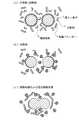
図1は、銀ナノ粒子を、トルエン, キシレン, テルピネオール, ミネラルスピリットなどの、室温付近では容易に蒸散することのない、比較的高沸点な非極性溶剤や低極性溶剤の中に安定に分散させたペーストが燒結する際の変化の様子を概念的に示す説明図であり、(a)は印刷前のペースト状態,(b)は加熱時に分散剤が除去される状態,(c)は樹脂収縮および低温燒結の状態をそれぞれ示している。
【0026】
(a)の状態では、銀ナノ粒子1の表面が、銀元素と配位可能な有機物、例えば金属イオンに対して還元作用を持つ2−メチルアミノエタノール,ジエタノールアミン,ジエチルメチルアミン,2−ジメチルアミノエタノール,メチルジエタノールアミンなどのアミン化合物や、アルキルアミン類,エチレンジアミン,アルキルアルコール類,エチレングリコール,プロピレングリコール,アルキルチオール類,エタンジチオールなどの分散剤2で被覆されている。
【0027】
この被覆作用により、銀ナノ粒子1のそれぞれは有機溶媒中に安定したかたちで分散する。
【0028】
なお、3は有機バインダー(例えば熱硬化性フェノール樹脂)、4は分散剤2を取り込むための捕捉物質(例えば酸無水物, 酸無水物誘導体)をそれぞれ示している。
【0029】
(b)の状態では、捕捉物質4が銀ナノ粒子1の表面部分の分散剤2を取り込んでいる。なお、分散剤2は銀ナノ粒子1の表面部分から剥離する。
【0030】
(c)の状態では、低温燒結した銀ナノ粒子同士が熱硬化性樹脂の収縮力で接触し、導通している。
【0031】
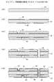
図2は、銀ナノペーストを用いたビルドアップ配線板の製造プロセス(積み上げ式)を示す断面図であり、その内容は次のようになっている。
(s11) コア基板11(エポキシ,ポリイミド,熱硬化性樹脂,アラミド不織布,ガラス布,ガラス不織布などからなる各種基板)を準備する。
(s12) エッチング処理により直径約50μm〜1mmの第1のビアホール12を形成する。
(s13) 銀ナノペースト13でコア基板11の表面に回路パターンを描画するとともに、銀ナノペースト13をビアホール12に充填した上で、加熱処理する。このとき、ビアホール12の銀ナノペーストは加熱硬化してその溶剤成分は飛散し、その金属成分がビアホール内周面に付着して、ビアホール12の全体がいわば「ちくわ状」になる。
(s14) 描画後のコア基板表面にフォトレジスト14を塗布してからエッチングすることにより、直径約50μm〜1mmの第2のビアホール15を形成する。
(s15) 銀ナノペースト16を用いて、ステップ(s13) と同様の描画・充填・加熱処理を実行し、この銀ナノペースト16のパターン(ランド)と銀ナノペースト13の回路パターンとを接続する。
(s16) フォトレジスト17を用いて、ステップ(s14) と同様の塗布・エッチング処理を実行し、直径約50μm〜1mmの第3のビアホール18を形成する。
(s17) 銀ナノペースト19を用いて、ステップ(s13) と同様の描画・充填・加熱処理を実行し、この銀ナノペースト19のパターン(ランド)と銀ナノペースト16のそれとを接続する。
【0032】
図3は、銀ナノペーストを用いたビルドアップ配線板の製造プロセス(両面印刷式)を示す説明図であり、その内容は次のようになっている。
(s21) コア基板21,21′(エポキシ,ポリイミド,熱硬化性樹脂,アラミド不織布,ガラス布,ガラス不織布などからなる各種基板)を準備する。
(s22) エッチング処理により直径約50μm〜1mmのビアホール22を形成する。
(s23) 銀ナノペースト23,23′でコア基板21の両面に回路パターンを描画するとともに、銀ナノペースト23,23′をビアホール12に充填した上で、加熱処理する。このとき、ビアホール22の全体は上述のように「ちくわ状」になる。
(s31) プリプレグなどの接合体31を準備する。
(s32) エッチング処理により直径約50μm〜1mmのビアホール32を形成して、当該ビアホールに従来の銀ペースト33を充填した上で、加熱処理する。このとき、ビアホール32の全体は上述のように「ちくわ状」になる。なお、従来の銀ペーストに代えて銀ナノペーストを用いてもよい。
(s41) ステップ(s21) 〜(s23) の処理後の基板21および21′の間に、ステップ(s31) ,(s32) の処理後の接合体31を挟んだ形の、この三つの部材を導電性接着剤で接合する。これにより、基板21の回路パターンと基板21′のそれとが接続される。
【0033】
図4は、銀ナノペーストを用いたビルドアップ配線板の製造プロセス(ドリル穴あけ式)を示す説明図であり、その内容は次のようになっている。
(s51) コア基板41(エポキシ,ポリイミド,熱硬化性樹脂,アラミド不織布,ガラス布,ガラス不織布などからなる各種基板)を準備する。
(s52) コア基板41の両面に銀ナノペースト42を用いたスクリーン印刷,インクジェットなどにより回路パターンを描画する。
(s53) 描画後のコア基板41の両面に表面にフォトレジスト43を塗布してからエッチングすることにより、直径約50μm〜1mmの第1のビアホール44を形成する。
(s54) ドリルで、この3層状態のコア基板41の両面間にまたがる直径約50μm〜1mmの第2のビアホール45を形成する。
(s55) このビアホール形成後のコア基板41の両面に銀ナノペースト46回路パターンを描画するとともに、銀ナノペースト46を各ビアホール44,45に充填した上で、加熱処理する。このとき、ビアホール44,45の全体はそれぞれ上述のように「ちくわ状」になる。この充填・加熱処理により、銀ナノペースト42の回路パターンと銀ナノペースト46のそれとが接続される。
【0034】
なお、上述の各ビアホールの径を大きくして、銀ナノペーストの代わりに従来の導電ペーストを充填してもよい。
【0035】
配線板に、平均粒子径7nmの銀ナノペーストをインクジェット印刷機により線幅25μmの回路パターンを描画し、これを180℃×30分の環境で加熱硬化させて所定の配線を形成したところ、その比抵抗は4×10⁻⁵Ω・cmであった。
【0036】
以下、本発明で用いる金属ナノペーストについて例示する。
【0037】
(例1)
市販されている銀の超微粒子分散液(商品名独立分散超微粒子パーフェクトシルバー 真空冶金(株))、具体的には、銀微粒子100質量部、アルキルアミンとして、ドデシルアミン15質量部、有機溶剤として、ターピネオール75質量部を含む、平均粒子径8nmの銀微粒子の分散液を利用した。
【0038】
導電性金属ペーストは、銀微粒子の分散液について、銀微粒子100質量部当たり、酸無水物として、Me−HHPA(メチルヘキサヒドロ無水フタル酸)を6.8質量部、熱硬化性樹脂として、レゾール型フェノール樹脂(群栄化学(株)製、PL−2211)を5質量部添加した。
【0039】
これらを混合した後、攪拌して調製された導電性金属ペーストに関して、それぞれメタルマスクで100μmのスルーホールを持つエポキシ基板上に膜厚50μm、縦横10×20mmの大きさで両面に塗布し、その表面状態(凝集状態)を確認した後、150℃×30分+210℃×60分で硬化した。
【0040】
別途、導電性金属ペーストに、チキソ剤もしくは希釈溶剤(トルエン)を加えて、その粘度をおよそ80Pa・sに調整し、ステンレス#500メッシュのスクリーン版でライン/スペース=25/25μmを印刷し、上記の硬化条件で硬化せしめ、その印刷性を評価した。
【0041】
図5に、導電性金属ペーストの組成と、塗布後の表面状態(凝集状態)、得られる熱硬化物の比抵抗、ならびに、粘度をおよそ80Pa・sに調整した際の印刷性に関する評価結果を併せて示す。なお、上記の導電性金属ペースト中に含有されるアミン化合物;ドデシルアミンと、酸無水物;Me−HHPA(メチルヘキサヒドロ無水フタル酸)の比率は、アミノ基1当たり、酸無水物1/2分子の割合である。
【0042】
(例2)
市販されている銀の超微粒子分散液(商品名独立分散超微粒子パーフェクトシルバー 真空冶金(株))を利用し、含まれる銀微粒子100質量部当たり、アルキルアミンとして、ドデシルアミン1質量部、有機溶剤として、ターピネオール75質量部を含む、平均粒子径8nmの銀微粒子の分散液を調製した。
【0043】
導電性金属ペーストは、前記組成の銀微粒子の分散液について、銀微粒子100質量部当たり、酸無水物として、Me−HHPA(メチルヘキサヒドロ無水フタル酸)を0.45質量部、熱硬化性樹脂として、レゾール型フェノール樹脂(群栄化学(株)製、PL−2211)を5質量部添加した。
【0044】
これらを混合した後、攪拌して調製された導電性金属ペーストに関して、それぞれメタルマスクで100μmのスルーホールを持つエポキシ基板上に膜厚50μm、縦横10×20mmの大きさで両面に塗布し、その表面状態(凝集状態)を確認した後、150℃×30分+210℃×60分で硬化した。
【0045】
別途、導電性金属ペーストに、チキソ剤もしくは希釈溶剤(トルエン)を加えて、その粘度をおよそ80Pa・sに調整し、ステンレス#500メッシュのスクリーン版でライン/スペース=25/25μmを印刷し、上記の硬化条件で硬化せしめ、その印刷性を評価した。
【0046】
図5に、導電性金属ペーストの組成と、塗布後の表面状態(凝集状態)、得られる熱硬化物の比抵抗、ならびに、粘度をおよそ80Pa・sに調整した際の印刷性に関する評価結果を併せて示す。なお、上記の導電性金属ペースト中に含有されるアミン化合物;ドデシルアミンと、酸無水物;Me−HHPA(メチルヘキサヒドロ無水フタル酸)の比率は、アミノ基1当たり、酸無水物1/2分子の割合である。
【0047】
(例3)
市販されている銀の超微粒子分散液(商品名独立分散超微粒子パーフェクトシルバー 真空冶金(株))を利用し、含まれる銀微粒子100質量部当たり、アルキルアミンとして、ドデシルアミン0.1質量部、有機溶剤として、ターピネオール75質量部を含む、平均粒子径8nmの銀微粒子の分散液を調製した。
【0048】
導電性金属ペーストは、前記組成の銀微粒子の分散液について、銀微粒子100質量部当たり、酸無水物として、Me−HHPA(メチルヘキサヒドロ無水フタル酸)を0.045質量部、熱硬化性樹脂として、レゾール型フェノール樹脂(群栄化学(株)製、PL−2211)を5質量部添加した。
【0049】
これらを混合した後、攪拌して調製された導電性金属ペーストに関して、それぞれメタルマスクで100μmのスルーホールを持つエポキシ基板上に膜厚50μm、縦横10×20mmの大きさで両面に塗布し、その表面状態(凝集状態)を確認した後、150℃×30分+210℃×60分で硬化した。
【0050】
別途、導電性金属ペーストに、チキソ剤もしくは希釈溶剤(トルエン)を加えて、その粘度をおよそ80Pa・sに調整し、ステンレス#500メッシュのスクリーン版でライン/スペース=25/25μmを印刷し、上記の硬化条件で硬化せしめ、その印刷性を評価した。
【0051】
図5に、導電性金属ペーストの組成と、塗布後の表面状態(凝集状態)、得られる熱硬化物の比抵抗、ならびに、粘度をおよそ80Pa・sに調整した際の印刷性に関する評価結果を併せて示す。なお、上記の導電性金属ペースト中に含有されるアミン化合物;ドデシルアミンと、酸無水物;Me−HHPA(メチルヘキサヒドロ無水フタル酸)の比率は、アミノ基1当たり、酸無水物1/2分子の割合である。
【0052】
(比較例1)
市販されている銀の超微粒子分散液(商品名独立分散超微粒子パーフェクトシルバー 真空冶金(株))を利用し、含まれる銀微粒子100質量部当たり、アルキルアミンとしてドデシルアミン0.05質量部、有機溶剤としてターピネオール75質量部を含む、平均粒子径8nmの銀微粒子の分散液を調製した。
【0053】
導電性金属ペーストは、前記組成の銀微粒子の分散液について、銀微粒子100質量部当たり、酸無水物として、Me−HHPA(メチルヘキサヒドロ無水フタル酸)を0.0225質量部、熱硬化性樹脂として、レゾール型フェノール樹脂(群栄化学(株)製、PL−2211)を5質量部添加した。
【0054】
これらを混合した後、攪拌して調製された導電性金属ペーストに関して、それぞれメタルマスクで100μmのスルーホールを持つエポキシ基板上に膜厚50μm、縦横10×20mmの大きさで両面に塗布し、その表面状態(凝集状態)を確認した後、150℃×30分+210℃×60分で硬化した。
【0055】
別途、導電性金属ペーストに、チキソ剤もしくは希釈溶剤(トルエン)を加えて、その粘度をおよそ80Pa・sに調整し、ステンレス#500メッシュのスクリーン版でライン/スペース=25/25μmを印刷し、上記の硬化条件で硬化せしめ、その印刷性を評価した。
【0056】
図5に、導電性金属ペーストの組成と、塗布後の表面状態(凝集状態)、得られる熱硬化物の比抵抗、ならびに、粘度をおよそ80Pa・sに調整した際の印刷性に関する評価結果を併せて示す。なお、上記の導電性金属ペースト中に含有されるアミン化合物;ドデシルアミンと、酸無水物;Me−HHPA(メチルヘキサヒドロ無水フタル酸)の比率は、アミノ基1当たり、酸無水物1/2分子の割合であるが、アミン化合物;ドデシルアミンは、銀微粒子の表面に一分子層のドデシルアミンが被覆するに要する量の1/2にしかならない量である。
【0057】
(比較例2)
市販されている銀の超微粒子分散液(商品名独立分散超微粒子パーフェクトシルバー 真空冶金(株))を利用し、含まれる銀微粒子を被覆しているアルキルアミン;ドデシルアミンを一旦除去し、再び有機溶剤として、ターピネオール75質量部を含み、ドデシルアミンの被覆層のない平均粒子径8nmの銀微粒子の分散液に調製した。
【0058】
導電性金属ペーストは、前記組成の銀微粒子の分散液について、銀微粒子100質量部当たり、酸無水物のMe−HHPA(メチルヘキサヒドロ無水フタル酸)を加えず、ただ、熱硬化性樹脂として、レゾール型フェノール樹脂(群栄化学(株)製、PL−2211)を5質量部添加した。
【0059】
これを混合した後、攪拌して調製された導電性金属ペーストに関して、それぞれメタルマスクで100μmのスルーホールを持つエポキシ基板上に膜厚50μm、縦横10×20mmの大きさで両面に塗布し、その表面状態(凝集状態)を確認した後、150℃×30分+210℃×60分で硬化した。
【0060】
別途、導電性金属ペーストに、チキソ剤もしくは希釈溶剤(トルエン)を加えて、その粘度をおよそ80Pa・sに調整し、ステンレス#500メッシュのスクリーン版でライン/スペース=25/25μmを印刷し、上記の硬化条件で硬化せしめ、その印刷性を評価した。
【0061】
図5に、導電性金属ペーストの組成と、塗布後の表面状態(凝集状態)、得られる熱硬化物の比抵抗、ならびに、粘度をおよそ80Pa・sに調整した際の印刷性に関する評価結果を併せて示す。
【0062】
図5に示される結果を対比させると、例1〜3と比較例1,2の結果から、銀微粒子100質量部当たり、トデシルアミンの含有量が減少するにつれ、導電性金属ペーストを加熱・硬化した硬化物における比抵抗は、次第に上昇している。また、銀微粒子100質量部当たり、トデシルアミンの含有量が0.1質量部を下回り、銀微粒子表面を被覆するトデシルアミンの一分子層に満たない範囲に到ると、急速に比抵抗の上昇が見出される。それと併せて、塗布されるペーストにおいて、室温においても、銀微粒子の凝集の発生が観測される。また、印刷性も、かかる凝集の発生に由来して、明らかに低下している。
【0063】
前記の対比では、アミン化合物の被覆層を設けない参照とした比較例2は別として、残る例1〜3と比較例1は、いずれも、銀微粒子表面を被覆するトデシルアミンの層を有するもの、銀微粒子100質量部当たり、トデシルアミンの含有量が減少し、均一な被覆層に欠損が生じやすくなるにつれ、室温においても、含まれる銀微粒子の凝集が生じ、印刷性もその影響を受け、低下していくと判断される。
【0064】
【発明の効果】
本発明は、このように、金,銀,銅などの金属またはこれらの合金の微粒子が液体中に安定に分散したペースト組成物、すなわち従来の微粒子のような凝集体が生じることのないペースト組成物を燒結させているので、多層配線板の回路パターンや、配線板表裏面間を結ぶ方向の導通用孔部の一層の微細化を図ることができる。
【図面の簡単な説明】
【図1】本発明の、銀ナノ粒子を、トルエン, キシレン, テルピネオール, ミネラルスピリットなどに安定に分散させたペーストが燒結する際の変化の様子を概念的に示す説明図であり、(a)は印刷前のペースト状態,(b)は加熱時に分散剤が除去される状態,(c)は樹脂収縮および低温燒結の状態を示している。
【図2】本発明の、銀ナノペーストを用いたビルドアップ配線板の製造プロセス(積み上げ式)を示す断面図である。
【図3】本発明の、銀ナノペーストを用いたビルドアップ配線板の製造プロセス(両面印刷式)を示す断面図である。
【図4】本発明の、銀ナノペーストを用いたビルドアップ配線板の製造プロセス(ドリル穴あけ式)を示す断面図である。
【図5】本発明の、銀ナノペーストの特性を示す説明図である。
【符号の説明】
1:銀ナノ粒子
2:分散剤
3:有機バインダー
4:捕捉物質
11:コア基板
12:第1のビアホール
13:銀ナノペースト
14:フォトレジスト
15:第2のビアホール
16:銀ナノペースト
17:フォトレジスト
18:第3のビアホール
19:銀ナノペースト
21,21′:コア基板
22:ビアホール22
23,23′:銀ナノペースト
31:プリプレグなどの接合体
32:ビアホール
33:従来の銀ペースト
41:コア基板
42:銀ナノペースト
43:フォトレジスト
44:第1のビアホール
45:第2のビアホール
46:銀ナノペースト[0001]
BACKGROUND OF THE INVENTION
The present invention uses a conductive paste made of fine metal particles stably dispersed in an organic solvent in the presence of, for example, amine, alcohol, thiol, etc., and build-up wiring board, plastic wiring board, printed wiring board, ceramic wiring board It is intended to form a fine circuit pattern on a multilayer wiring board such as the above and a fine hole for conduction in a direction connecting the front and back surfaces of the wiring board.
[0002]
That is, for example, it can be applied to screen-type microprinting that can be handled like a liquid, application to a microstructural surface, and further to a three-dimensional mounting region.
[0003]
Here, the circuit pattern includes a wiring pattern. In the following description, the term “via hole” is used as necessary to indicate an arbitrary conduction hole in the direction connecting the front and back surfaces of the wiring board.
[0004]
In recent years, various electronic devices such as mobile phones and personal computers have been reduced in size, weight, performance, speed, and functionality, and further miniaturization of multilayer circuit boards and conductive holes has been required. Therefore, the present invention meets such a demand.
[0005]
[Prior art]
Conventionally, as a method of forming a circuit pattern on a wiring board,
・ Subtractive method that leaves only the desired conductor pattern on the copper-clad laminate and removes other parts by etching. ・ Generates negative pattern plating resist on the copperless laminate and forms the conductor pattern by electroless plating. Many additive methods are used.
[0006]
All of these circuit pattern forming methods are complicated in operation and a large amount of processing waste liquid is generated, so that improvement in cost and environment has been demanded first.
[0007]
In order to solve this, a conductive pattern is formed on a copper-free laminate using a conductive silver paste.
[0008]
In the sintering process of this conductor pattern,
・ The average particle size of the paste is 0.1-20μm
The wiring width of the conductor pattern is 50 μm or more. The temperature for baking the paste is 500 ° C. or more.
[0009]
[Problems to be solved by the invention]
The degree to which the conductor pattern to be formed can be made finer depends on the size of the metal particles blended in the conductive paste. Therefore, in the conventional method for forming a conductor pattern using metal particles having a particle size of about 50 μm / 50 μm, the line / space is the limit.
[0010]
In addition, the metal fine particles (nanoparticles: for example, an average particle diameter of 100 nm or less) itself have a property that the particles are melted at room temperature due to their high surface activity and form aggregates of several tens to several hundreds units. . Therefore, it is not suitable for fine printing of a conductor pattern only by making the metal blended in the conductive paste into fine particles.
[0011]
Further, due to this cohesive property, a sintered conductive portion could not be formed with a conductive paste inside the fine via hole. Conventionally, the minimum diameter of a via hole that can form a sintered conductive portion is about 100 μm.
[0012]
Therefore, in the present invention, by using a paste composition in which the surface of metal fine particles is coated with an organic compound capable of coordinating with a metal element contained therein and stably dispersed in a liquid, It is an object to further refine the conduction hole in the direction connecting the front and back surfaces of the plate.
[0013]
[Means for Solving the Problems]
The present invention solves this problem as follows.
(1) A paste composition in which metal fine particles having an average particle diameter of 1 to 100 nm are coated with an organic compound capable of coordinating with a metal element contained in the metal fine particles and stably dispersed in a liquid. A circuit pattern obtained by sintering at a temperature of 250 ° C. or lower is formed on the surface portion of the wiring board.
(2) Paste composition in which metal fine particles having an average particle diameter of 1 to 100 nm are coated with an organic compound capable of coordinating with a metal element contained in the metal fine particles and stably dispersed in a liquid Is formed in the hole for conduction in the direction connecting the front and back surfaces of the wiring board.
(3) A paste composition in which metal fine particles having an average particle diameter of 1 to 100 nm are coated with an organic compound capable of coordinating with a metal element contained in the metal fine particles and stably dispersed in a liquid. Then, draw a circuit pattern on the surface of the wiring board,
The coating layer is removed by heating the wiring board at a temperature of 250 ° C. or less, and the metal fine particles of the drawing circuit pattern are sintered together.
(4) A paste composition in which metal fine particles having an average particle diameter of 1 to 100 nm are coated with an organic compound capable of coordinating with a metal element contained in the metal fine particles and stably dispersed in a liquid. Is filled into the hole for conduction in the direction connecting the front and back surfaces of the wiring board,
The coating layer is removed by heating at a temperature of 250 ° C. or lower, and the metal fine particles in the hole for conduction are sintered.
(6) Gold, silver, copper, platinum, palladium, rhodium, osmium, ruthenium, iridium, iron, tin, zinc, cobalt, nickel, chromium, titanium, tantalum, as the metal fine particles of (1) to (4) above Fine particles of at least one kind of metal among tungsten, indium and silicon, or fine particles of an alloy made of two or more kinds of metals are used.
[0014]
As described above, the present invention provides a paste composition in which fine particles (nanoparticles) of the above metals such as gold, silver and copper or their alloys are stably dispersed in an organic solvent, that is, the above aggregates such as conventional fine particles. Thus, a fine circuit pattern and a fine conductive portion in the conductive hole are formed in a form in which a paste composition that does not cause sinter is sintered. The fine particles are stable at room temperature.
[0015]
Various methods such as ink jet, screen printing, dispenser, impregnation, and spin coating may be used to draw the paste made of metal fine particles on the wiring board and fill the hole for conduction.
[0016]
The metal fine particles are present in a stable form dispersed in an organic solvent, as described above, because the surface of the compound can coordinate with the metal element (for example, amine, alcohol, phenol, thiol, etc.). This is because it is coated with a dispersant.
[0017]
This coordination bondable compound is removed by a chemical reaction during subsequent heating. This ensures the stability of the metal fine particles before heating and the dense sintered state of the metal fine particles after being heated and melted.
[0018]
The paste made of the metal fine particles has an average particle diameter of, for example, about 0.1 to 10 nm, and has more particles in the plane and thickness direction than the conventional silver paste. Therefore, even when a fine pattern or an ultrathin film (for example, a film having an average particle diameter of 7 nm and a thickness of 4 μm) is formed, sufficient conductive performance can be achieved. For stable conduction, a film thickness of 4 times or more the particle diameter is required. Incidentally, the conventional thin film is, for example, a film having an average particle diameter of 3 μm and a thickness of 20 μm.
[0019]
Further, since the paste has a low viscosity, it flows like a liquid, and the sintering proceeds only after the heat treatment. Because of this low viscosity, the paste can be filled into the fine holes for conduction (via holes).
[0020]
The line / space of the fine circuit pattern is, for example, 25 μm / 25 μm, and the diameter of the conductive hole where the conductive portion can be formed is about 50 μm to 1 mm. The sintering temperature of the paste is also lower than that of the conventional one, for example, 250 ° C. or less.
[0021]
Furthermore, it is effective to use these fine particles in a stable state together with a conventional conductive paste having an average particle size on the order of μm.
[0022]
For example, when the silver fine particles of the present invention are mixed with the conventional silver paste, the silver fine particles enter between the large silver particles after sintering, and the entire bonded state is stabilized.
[0023]
In addition, when the copper paste is used in combination, the contact resistance due to the thin copper oxide film can be modified to lower the overall contact resistance.
[0024]
DETAILED DESCRIPTION OF THE INVENTION
Embodiments of the present invention will be described below.
For convenience of explanation, “silver nanoparticles having an average particle diameter of 7 nm” is used as an example of metal fine particles as necessary, and the paste is referred to as “silver nano paste”. However, the present invention is of course limited to these silver nanoparticles. Is not to be done.
[0025]
Figure 1 shows the stable dispersion of silver nanoparticles in a non-polar or low-polar solvent with a relatively high boiling point, such as toluene, xylene, terpineol, mineral spirit, etc. that does not easily evaporate near room temperature. FIG. 3 is an explanatory diagram conceptually showing a state of change when a paste is sintered, (a) is a paste state before printing, (b) is a state in which a dispersant is removed during heating, and (c) is a resin shrinkage. And shows the state of low-temperature sintering.
[0026]
In the state of (a), the surface of the
[0027]
Due to this coating action, each of the
[0028]
Reference numeral 3 represents an organic binder (for example, thermosetting phenol resin), and 4 represents a trapping substance (for example, acid anhydride or acid anhydride derivative) for taking up the
[0029]
In the state (b), the trapping substance 4 takes in the
[0030]
In the state of (c), the silver nanoparticles sintered at low temperature are brought into contact with each other by the shrinkage force of the thermosetting resin and are conducted.
[0031]
FIG. 2 is a cross-sectional view showing a manufacturing process (stacking type) of a build-up wiring board using silver nanopaste, and the contents are as follows.
(s11) A core substrate 11 (various substrates made of epoxy, polyimide, thermosetting resin, aramid nonwoven fabric, glass fabric, glass nonwoven fabric, etc.) is prepared.
(s12) A first via
(s13) A circuit pattern is drawn on the surface of the
(s14) A second via
(s15) Using the
(s16) Using the
(s17) Using the
[0032]
FIG. 3 is an explanatory view showing a manufacturing process (double-sided printing type) of a build-up wiring board using silver nanopaste, and the contents thereof are as follows.
(s21)
(s22) A via
(s23) A circuit pattern is drawn on both surfaces of the
(s31) A joined
(s32) A via
(s41) The three members having a shape in which the bonded
[0033]
FIG. 4 is an explanatory view showing a manufacturing process (drill drilling type) of a build-up wiring board using silver nanopaste, and the contents thereof are as follows.
(s51) A core substrate 41 (various substrates made of epoxy, polyimide, thermosetting resin, aramid nonwoven fabric, glass fabric, glass nonwoven fabric, etc.) is prepared.
(s52) A circuit pattern is drawn on both surfaces of the
(s53) First via
(s54) A second via
(s55) A circuit pattern of the
[0034]
In addition, the diameter of each of the above-described via holes may be increased, and a conventional conductive paste may be filled instead of the silver nano paste.
[0035]
When a circuit pattern having a line width of 25 μm was drawn on a wiring board with a silver nanopaste having an average particle diameter of 7 nm by an ink jet printer, this was heated and cured in an environment of 180 ° C. × 30 minutes to form a predetermined wiring. The specific resistance was 4 × 10⁻⁵ Ω · cm.
[0036]
Hereinafter, metal nano paste used in the present invention will be exemplified.
[0037]
(Example 1)
Commercially available silver ultrafine particle dispersion (trade name independent dispersed ultrafine particle Perfect Silver Vacuum Metallurgy Co., Ltd.), specifically, silver fine particle 100 parts by mass, alkylamine, dodecylamine 15 parts by mass, organic solvent A dispersion of silver fine particles having an average particle diameter of 8 nm and containing 75 parts by mass of terpineol was used.
[0038]
The conductive metal paste was prepared by adding 6.8 parts by weight of Me-HHPA (methylhexahydrophthalic anhydride) as an acid anhydride and 100% by weight of silver fine particle dispersion as a thermosetting resin. 5 parts by mass of type phenol resin (manufactured by Gunei Chemical Co., Ltd., PL-2211) was added.
[0039]
After mixing these, the conductive metal paste prepared by stirring was applied on both sides with a metal mask on a 100 μm through-hole epoxy film with a film thickness of 50 μm and a size of 10 × 20 mm vertically and horizontally. After confirming the surface state (aggregation state), it was cured at 150 ° C. × 30 minutes + 210 ° C. × 60 minutes.
[0040]
Separately, a thixotropic agent or a diluting solvent (toluene) is added to the conductive metal paste, the viscosity is adjusted to about 80 Pa · s, and line / space = 25/25 μm is printed on a stainless steel # 500 mesh screen plate, It hardened | cured on said hardening conditions and evaluated the printability.
[0041]
FIG. 5 shows the evaluation results regarding the composition of the conductive metal paste, the surface state after application (aggregation state), the specific resistance of the obtained thermoset, and the printability when the viscosity is adjusted to about 80 Pa · s. Also shown. The ratio of the amine compound contained in the above conductive metal paste; dodecylamine and acid anhydride; Me-HHPA (methylhexahydrophthalic anhydride) is 1/2 acid anhydride per amino group. The percentage of molecules.
[0042]
(Example 2)
Using commercially available silver ultrafine particle dispersion (trade name independent dispersed ultrafine particle Perfect Silver Vacuum Metallurgy Co., Ltd.), 1 part by mass of dodecylamine as an alkylamine per 100 parts by mass of silver fine particles contained, organic solvent A dispersion of silver fine particles having an average particle diameter of 8 nm and containing 75 parts by mass of terpineol was prepared.
[0043]
As for the conductive metal paste, 0.45 parts by mass of Me-HHPA (methylhexahydrophthalic anhydride) as an acid anhydride per 100 parts by mass of silver fine particles in the dispersion of silver fine particles having the above composition, a thermosetting resin As a result, 5 parts by mass of a resol type phenol resin (manufactured by Gunei Chemical Co., Ltd., PL-2211) was added.
[0044]
After mixing these, the conductive metal paste prepared by stirring was applied on both sides with a metal mask on a 100 μm through-hole epoxy film with a film thickness of 50 μm and a size of 10 × 20 mm vertically and horizontally. After confirming the surface state (aggregation state), it was cured at 150 ° C. × 30 minutes + 210 ° C. × 60 minutes.
[0045]
Separately, a thixotropic agent or a diluting solvent (toluene) is added to the conductive metal paste, the viscosity is adjusted to about 80 Pa · s, and line / space = 25/25 μm is printed on a stainless steel # 500 mesh screen plate, It hardened | cured on said hardening conditions and evaluated the printability.
[0046]
FIG. 5 shows the evaluation results regarding the composition of the conductive metal paste, the surface state after application (aggregation state), the specific resistance of the obtained thermoset, and the printability when the viscosity is adjusted to about 80 Pa · s. Also shown. The ratio of the amine compound contained in the above conductive metal paste; dodecylamine and acid anhydride; Me-HHPA (methylhexahydrophthalic anhydride) is 1/2 acid anhydride per amino group. The percentage of molecules.
[0047]
(Example 3)
Using commercially available silver ultrafine particle dispersion (trade name independent dispersed ultrafine particle Perfect Silver Vacuum Metallurgy Co., Ltd.), per 100 parts by mass of silver fine particles contained, 0.1 parts by mass of dodecylamine as alkylamine, As an organic solvent, a dispersion of silver fine particles having an average particle diameter of 8 nm and containing 75 parts by mass of terpineol was prepared.
[0048]
The conductive metal paste is 0.045 parts by mass of Me-HHPA (methylhexahydrophthalic anhydride) as an acid anhydride per 100 parts by mass of the silver fine particles in the dispersion of silver fine particles having the above composition, a thermosetting resin. As a result, 5 parts by mass of a resol type phenol resin (manufactured by Gunei Chemical Co., Ltd., PL-2211) was added.
[0049]
After mixing these, the conductive metal paste prepared by stirring was applied on both sides with a metal mask on a 100 μm through-hole epoxy film with a film thickness of 50 μm and a size of 10 × 20 mm vertically and horizontally. After confirming the surface state (aggregation state), it was cured at 150 ° C. × 30 minutes + 210 ° C. × 60 minutes.
[0050]
Separately, a thixotropic agent or a diluting solvent (toluene) is added to the conductive metal paste, the viscosity is adjusted to about 80 Pa · s, and line / space = 25/25 μm is printed on a stainless steel # 500 mesh screen plate, It hardened | cured on said hardening conditions and evaluated the printability.
[0051]
FIG. 5 shows the evaluation results regarding the composition of the conductive metal paste, the surface state after application (aggregation state), the specific resistance of the obtained thermoset, and the printability when the viscosity is adjusted to about 80 Pa · s. Also shown. The ratio of the amine compound contained in the above conductive metal paste; dodecylamine and acid anhydride; Me-HHPA (methylhexahydrophthalic anhydride) is 1/2 acid anhydride per amino group. The percentage of molecules.
[0052]
(Comparative Example 1)
Using commercially available silver ultrafine particle dispersion (trade name independent dispersed ultrafine particle Perfect Silver Vacuum Metallurgical Co., Ltd.), 0.05 parts by mass of dodecylamine as an alkylamine per 100 parts by mass of silver fine particles contained, organic A dispersion of silver fine particles having an average particle diameter of 8 nm and containing 75 parts by mass of terpineol as a solvent was prepared.
[0053]
As for the conductive metal paste, 0.0225 parts by mass of Me-HHPA (methylhexahydrophthalic anhydride) as an acid anhydride per 100 parts by mass of the silver fine particles in the dispersion of silver fine particles having the above composition, a thermosetting resin As a result, 5 parts by mass of a resol type phenol resin (manufactured by Gunei Chemical Co., Ltd., PL-2211) was added.
[0054]
After mixing these, the conductive metal paste prepared by stirring was applied on both sides with a metal mask on a 100 μm through-hole epoxy film with a film thickness of 50 μm and a size of 10 × 20 mm vertically and horizontally. After confirming the surface state (aggregation state), it was cured at 150 ° C. × 30 minutes + 210 ° C. × 60 minutes.
[0055]
Separately, a thixotropic agent or a diluting solvent (toluene) is added to the conductive metal paste, the viscosity is adjusted to about 80 Pa · s, and line / space = 25/25 μm is printed on a stainless steel # 500 mesh screen plate, It hardened | cured on said hardening conditions and evaluated the printability.
[0056]
FIG. 5 shows the evaluation results regarding the composition of the conductive metal paste, the surface state after application (aggregation state), the specific resistance of the obtained thermoset, and the printability when the viscosity is adjusted to about 80 Pa · s. Also shown. The ratio of the amine compound contained in the above conductive metal paste; dodecylamine and acid anhydride; Me-HHPA (methylhexahydrophthalic anhydride) is 1/2 acid anhydride per amino group. Although it is a ratio of the molecule, the amine compound; dodecylamine is an amount that is only ½ of the amount required for the monomolecular layer of dodecylamine to be coated on the surface of the silver fine particles.
[0057]
(Comparative Example 2)
Using a commercially available silver ultrafine particle dispersion (trade name independent ultrafine particle Perfect Silver Vacuum Metallurgy Co., Ltd.), the alkylamine covering the silver fine particles contained therein is removed once; dodecylamine is once again organic As a solvent, a dispersion of silver fine particles containing 75 parts by mass of terpineol and having no coating layer of dodecylamine and having an average particle diameter of 8 nm was prepared.
[0058]
The conductive metal paste does not add acid anhydride Me-HHPA (methylhexahydrophthalic anhydride) per 100 parts by mass of silver fine particles in the dispersion of silver fine particles having the above composition, but as a thermosetting resin, 5 parts by mass of a resol type phenol resin (manufactured by Gunei Chemical Co., Ltd., PL-2211) was added.
[0059]
After mixing this, the conductive metal paste prepared by stirring was applied on both sides with a metal mask on a 100 μm through-hole epoxy film having a film thickness of 50 μm and a vertical and horizontal size of 10 × 20 mm. After confirming the surface state (aggregation state), it was cured at 150 ° C. × 30 minutes + 210 ° C. × 60 minutes.
[0060]
Separately, a thixotropic agent or a diluting solvent (toluene) is added to the conductive metal paste, the viscosity is adjusted to about 80 Pa · s, and line / space = 25/25 μm is printed on a stainless steel # 500 mesh screen plate, It hardened | cured on said hardening conditions and evaluated the printability.
[0061]
FIG. 5 shows the evaluation results regarding the composition of the conductive metal paste, the surface state after application (aggregation state), the specific resistance of the obtained thermoset, and the printability when the viscosity is adjusted to about 80 Pa · s. Also shown.
[0062]
When the results shown in FIG. 5 are compared, from the results of Examples 1 to 3 and Comparative Examples 1 and 2, the conductive metal paste was heated and cured as the todecylamine content decreased per 100 parts by mass of the silver fine particles. The specific resistance in the cured product is gradually increasing. In addition, when the content of todecylamine is less than 0.1 parts by mass per 100 parts by mass of the silver fine particles and reaches a range of less than one molecular layer of todecylamine covering the surface of the silver fine particles, the specific resistance is rapidly increased. It is. In addition, in the paste to be applied, the occurrence of aggregation of silver fine particles is observed even at room temperature. Also, the printability is clearly reduced due to the occurrence of such aggregation.
[0063]
In the above comparison, apart from Comparative Example 2 which was referred to without providing an amine compound coating layer, the remaining Examples 1 to 3 and Comparative Example 1 both had a todecylamine layer covering the silver fine particle surface, As the content of todecylamine per 100 parts by mass of silver fine particles decreases and defects are more likely to occur in the uniform coating layer, aggregation of the silver fine particles contained occurs at room temperature, and the printability is affected and decreased. It is judged to go.
[0064]
【The invention's effect】
As described above, the present invention provides a paste composition in which fine particles of a metal such as gold, silver, copper, or an alloy thereof are stably dispersed in a liquid, that is, a paste composition in which aggregates such as conventional fine particles are not generated. Since the objects are sintered, it is possible to further miniaturize the circuit pattern of the multilayer wiring board and the conduction hole in the direction connecting the front and back surfaces of the wiring board.
[Brief description of the drawings]
BRIEF DESCRIPTION OF DRAWINGS FIG. 1 is an explanatory diagram conceptually showing a change state when a paste in which silver nanoparticles of the present invention are stably dispersed in toluene, xylene, terpineol, mineral spirit or the like is sintered, (a) Is a paste state before printing, (b) is a state in which the dispersant is removed during heating, and (c) is a state of resin shrinkage and low-temperature sintering.
FIG. 2 is a cross-sectional view showing a manufacturing process (stacking type) of a build-up wiring board using silver nanopaste according to the present invention.
FIG. 3 is a sectional view showing a manufacturing process (double-sided printing type) of a build-up wiring board using silver nanopaste according to the present invention.
FIG. 4 is a cross-sectional view showing a manufacturing process (drilling type) of a build-up wiring board using silver nanopaste according to the present invention.
FIG. 5 is an explanatory diagram showing the characteristics of the silver nanopaste of the present invention.
[Explanation of symbols]
1: Silver nanoparticles 2: Dispersant 3: Organic binder 4: Capture substance 11: Core substrate 12: First via hole 13: Silver nano paste 14: Photoresist 15: Second via hole 16: Silver nano paste 17: Photo Resist 18: Third via hole 19:
23, 23 ': Silver nano paste 31: Joint body such as prepreg 32: Via hole 33: Conventional silver paste 41: Core substrate 42: Silver nano paste 43: Photoresist 44: First via hole 45: Second via hole 46 : Silver nano paste
Claims (12)
Translated fromJapanese該導電性金属ペーストを用いて形成される導体パターンが、回路パターンとして、配線板表面部分に形成されており、
前記導体パターンの形成に利用される導電性金属ペーストは、
平均粒径が1〜100nmである金属微粒子を、室温付近では容易に蒸散することのない非極性溶剤ならびに低極性溶剤からなる群から選択される溶剤中に安定に分散してなるペースト組成物であり、
該平均粒径が1〜100nmである金属微粒子は、その金属表面は、当該金属微粒子に含まれる金属元素に対して配位結合可能な有機化合物で被覆されてなる被覆層を具え、該有機化合物の被覆層を保持する状態で、前記液体中に安定に分散されており、
該ペースト組成物中には、加熱時に、前記有機化合物に作用可能な捕捉物質が含まれており、
前記導体パターンは、
配線板表面部分に塗布された前記導電性金属ペーストに対して、250℃以下の温度で加熱処理を施し、該金属微粒子の金属表面を被覆している有機化合物を、前記捕捉物質の作用によって、剥離させ、
前記有機化合物の被覆層の剥離がなされた金属微粒子相互の金属表面を接触させ、該金属微粒子相互の焼結を行わせることで形成される導体パターンである
ことを特徴とする多層配線板。A multilayer wiring board comprising a conductor pattern formed using a conductive metal paste,
The conductor pattern formed using the conductive metal paste is formed on the surface of the wiring board as a circuit pattern,
The conductive metal paste used for forming the conductor pattern is:
Metal fine particles having an average particle diameter of 1 to 100nm,a paste composition obtained byeasily and stably dispersed in asolvent selected from transpiration nonpolar solvent and the group consisting of low polarity solvent not to the vicinity of room temperatureYes,
The metal fine particles having an average particle diameter of 1 to 100 nm include a coating layer in which the metal surface is coated with an organic compound capable of coordinating and bonding to a metal element contained in the metal fine particles, and the organic compound Is stably dispersed in the liquid in a state of holding the coating layer of
The paste composition contains a trapping substance capable of acting on the organic compound when heated,
The conductor pattern is
The conductive metal paste applied to the surface portion of the wiring boardis subjected to a heat treatment at a temperature of 250 ° C. or less, and an organic compound covering the metal surface of the metal fine particles is obtained by the action of the trapping substance, Exfoliate,
A multi-layeredconductive pattern formedbybringing metal fine particles from which the coating layer of the organic compound has been peeled into contact with each other and causing the metal fine particles to sinter. Wiring board.
該導電性金属ペーストを用いて形成される導通部は、配線板表裏面間を結ぶ方向の導通用孔部に形成されており、
前記導通部の形成に利用される導電性金属ペーストは、
平均粒径が1〜100nmである金属微粒子を、室温付近では容易に蒸散することのない非極性溶剤ならびに低極性溶剤からなる群から選択される溶剤中に安定に分散してなるペースト組成物であり、
該平均粒径が1〜100nmである金属微粒子は、その金属表面は、当該金属微粒子に含まれる金属元素に対して配位結合可能な有機化合物で被覆されてなる被覆層を具え、該有機化合物の被覆層を保持する状態で、前記液体中に安定に分散されており、
該ペースト組成物中には、加熱時に、前記有機化合物に作用可能な捕捉物質が含まれており、
前記導通部は、
配線板表裏面間を結ぶ方向の導通用孔部に塗布された前記導電性金属ペーストに対して、250℃以下の温度で加熱処理を施し、該金属微粒子の金属表面を被覆している有機化合物を、前記捕捉物質の作用によって、剥離させ、
前記有機化合物の被覆層の剥離がなされた金属微粒子相互の金属表面を接触させ、該金属微粒子相互の焼結を行わせることで形成される導通部である
ことを特徴とする多層配線板。A multilayer wiring board having a conductive portion formed using a conductive metal paste,
The conductive portion formed using the conductive metal paste is formed in a conductive hole in a direction connecting the front and back surfaces of the wiring board,
The conductive metal paste used for forming the conductive part is
Metal fine particles having an average particle diameter of 1 to 100nm,a paste composition obtained byeasily and stably dispersed in asolvent selected from transpiration nonpolar solvent and the group consisting of low polarity solvent not to the vicinity of room temperatureYes,
The metal fine particles having an average particle diameter of 1 to 100 nm include a coating layer in which the metal surface is coated with an organic compound capable of coordinating and bonding to a metal element contained in the metal fine particles, and the organic compound Is stably dispersed in the liquid in a state of holding the coating layer of
The paste composition contains a trapping substance capable of acting on the organic compound when heated,
The conduction part is
An organic compoundin which the conductive metal paste applied to the hole for conduction in the direction connecting the front and back surfaces of the wiring boardis subjected to a heat treatment at a temperatureof 250 ° C. or lessto cover the metal surface of the metal fine particles Is peeled off by the action of the trapping substance,
Multilayer, whereinthe peeling of the coating layer of an organic compound by contacting the fine metal particles each other metallic surface which has been made, <br/> itis conducting portionformed by causing the sintering of the fine metal particles each other Wiring board.
金,銀,銅,白金,パラジウム,ロジウム,オスミウム,ルテニウム,イリジウム,鉄,錫,亜鉛,コバルト,ニッケル,クロム,チタン,タンタル,タングステン,インジウム,ケイ素の中の少なくとも一種類の金属の微粒子、または二種類以上の金属からなる合金の微粒子である、
ことを特徴とする、請求項1または2に記載の多層配線板。The fine metalparticles,
Fine particles of at leastone metal among gold, silver, copper, platinum, palladium, rhodium, osmium, ruthenium, iridium, iron, tin, zinc, cobalt, nickel, chromium, titanium, tantalum, tungsten, indium, silicon, Or an alloy particle composed oftwo or more metals,
The multilayer wiring board accordingto claim 1, wherein the multilayer wiring board is provided.
該導電性金属ペーストを用いて形成される導体パターンが、回路パターンとして、配線板表面部分に形成されており、
前記導体パターンの形成に利用される導電性金属ペーストは、
平均粒径が1〜100nmである金属微粒子を、室温付近では容易に蒸散することのない非極性溶剤ならびに低極性溶剤からなる群から選択される溶剤中に安定に分散してなるペースト組成物であり、
該平均粒径が1〜100nmである金属微粒子は、その金属表面は、当該金属微粒子に含まれる金属元素に対して配位結合可能な有機化合物で被覆されてなる被覆層を具え、該有機化合物の被覆層を保持する状態で、前記液体中に安定に分散されており、
該ペースト組成物中には、加熱時に、前記有機化合物に作用可能な捕捉物質が含まれており、
該多層配線板を作製する工程は、
該配線板表面部分に、前記導電性金属ペーストを用いて、該回路パターンを描画する工程と、
前記描画工程において、配線板表面部分に塗布された前記導電性金属ペーストに対して、250℃以下の温度で加熱処理を施し、該金属微粒子の金属表面を被覆している有機化合物を、前記捕捉物質の作用によって、剥離させ、
前記有機化合物の被覆層の剥離がなされた金属微粒子相互の金属表面を接触させ、該金属微粒子相互の焼結を行わせることで、前記導体パターンを形成する工程とを有する
ことを特徴とする多層配線板の作製方法。Awayto produce a multilayer wiring board comprising a conductive pattern formed using a conductive metalpaste,
The conductor pattern formed using the conductive metal paste is formed on the surface of the wiring board as a circuit pattern,
The conductive metal paste used for forming the conductor pattern is:
Metal fine particles having an average particle diameter of 1 to 100nm,a paste composition obtained byeasily and stably dispersed in asolvent selected from transpiration nonpolar solvent and the group consisting of low polarity solvent not to the vicinity of room temperatureYes,
The metal fine particles having an average particle diameter of 1 to 100 nm include a coating layer in which the metal surface is coated with an organic compound capable of coordinating and bonding to a metal element contained in the metal fine particles, and the organic compound Is stably dispersed in the liquid in a state of holding the coating layer of
The paste composition contains a trapping substance capable of acting on the organic compound when heated,
The step of producing the multilayer wiring board includes:
Onthe wiring board surfaceportion, by using the conductive metal paste,a step of drawingthe circuitpatterns,
In the drawing step, the conductive metal paste applied to the surface portion of the wiring boardis subjected to a heattreatment at a temperature of 250 ° C. or less, and the organic compound covering the metal surface of the metal fine particles is captured. By the action of the substance,
Forming the conductor patternby bringing the metal surfaces of the metal fine particles from which the coating layer of the organic compound has been peeled into contact witheach otherand causing the metal fine particles to sinterwitheach other. A method forproducing a featured multilayer wiring board.
該導電性金属ペーストを用いて形成される導通部は、配線板表裏面間を結ぶ方向の導通用孔部に形成されており、
前記導通部の形成に利用される導電性金属ペーストは、
平均粒径が1〜100nmである金属微粒子を、室温付近では容易に蒸散することのない非極性溶剤ならびに低極性溶剤からなる群から選択される溶剤中に安定に分散してなるペースト組成物であり、
該平均粒径が1〜100nmである金属微粒子は、その金属表面は、当該金属微粒子に含まれる金属元素に対して配位結合可能な有機化合物で被覆されてなる被覆層を具え、該有機化合物の被覆層を保持する状態で、前記液体中に安定に分散されており、
該ペースト組成物中には、加熱時に、前記有機化合物に作用可能な捕捉物質が含まれており、
該多層配線板を作製する工程は、
該配線板表裏面間を結ぶ方向の導通用孔部に、前記導電性金属ペーストを充填し、少なくとも、該導通用孔部の内周表面と接する導電性金属ペーストの充填層を形成する工程と、
前記充填層形成工程で、配線板表裏面間を結ぶ方向の導通用孔部に充填された前記導電性金属ペーストに対して、250℃以下の温度で加熱処理を施し、該金属微粒子の金属表面を被覆している有機化合物を、前記捕捉物質の作用によって、剥離させ、
前記有機化合物の被覆層の剥離がなされた金属微粒子相互の金属表面を接触させ、該金属微粒子相互の焼結を行わせること、前記導通部を形成される工程とを有する
ことを特徴とする、多層配線板の作製方法。A method for producing a multilayer wiring board having a conductive portion formed using a conductive metal paste,
The conductive portion formed using the conductive metal paste is formed in a conductive hole in a direction connecting the front and back surfaces of the wiring board,
The conductive metal paste used for forming the conductive part is
A paste composition in which metal fine particles having an average particle diameter of 1 to 100 nm are stably dispersed in a solvent selected from the group consisting of nonpolar solvents and low polarity solvents that do not easily evaporate near room temperature. Yes,
The metal fine particles having an average particle diameter of 1 to 100 nm include a coating layer in which the metal surface is coated with an organic compound capable of coordinating and bonding to a metal element contained in the metal fine particles, and the organic compound Is stably dispersed in the liquid in a state of holding the coating layer of
The paste composition contains a trapping substance capable of acting on the organic compound when heated,
The step of producing the multilayer wiring board includes:
The conducting hole in the direction connecting betweenthe wiring board front and backsurfaces, filledwith the conductive metal paste,and forming at least a filling layer of a conductive metal paste which is in contact with the inner circumferential surface of the conductor-class hole ,
In the filling layer forming step, the conductive metal paste filled in the hole for conduction in the direction connecting the front and back surfaces of the wiring boardis subjected to heattreatment at a temperature of 250 ° C. or less, and the metal surface of the metal fine particles The organic compound covering the substrate is peeled off by the action of the trapping substance,
A step of bringing the metal surfaces of the metal fine particles from which the coating layer of the organic compound has been peeled into contact witheach otherto cause the metal fine particles to sinter,and the step of forming the conductive portion. A method forproducing a multilayer wiring board, which is characterized.
金,銀,銅,白金,パラジウム,ロジウム,オスミウム,ルテニウム,イリジウム,鉄,錫,亜鉛,コバルト,ニッケル,クロム,チタン,タンタル,タングステン,インジウム,ケイ素の中の少なくとも一種類の金属の微粒子、または二種類以上の金属からなる合金の微粒子である、
ことを特徴とする請求項4または5に記載の多層配線板の作製方法。The fine metalparticles,
Fine particles of at leastone metal among gold, silver, copper, platinum, palladium, rhodium, osmium, ruthenium, iridium, iron, tin, zinc, cobalt, nickel, chromium, titanium, tantalum, tungsten, indium, silicon, Or an alloy particle composed oftwo or more metals,
The method for producinga multilayer wiring board according to claim 4 or 5, wherein:
ことを特徴とする、請求項1〜3のいずれか一項に記載の多層配線板。The multilayer wiring board according to claim 1, wherein the trapping substance is an acid anhydride.
ことを特徴とする、請求項1〜3、7のいずれか一項に記載の多層配線板。The multilayer wiring board according to claim 1, wherein an organic binder is contained in the paste composition.
ことを特徴とする、請求項8に記載の多層配線板。The multilayer wiring board according to claim 8, wherein the paste composition contains a thermosetting phenol resin as an organic binder.
ことを特徴とする、請求項4〜6のいずれか一項に記載の多層配線板の作製方法。The method for producing a multilayer wiring board according to claim 4, wherein the trapping substance is an acid anhydride.
ことを特徴とする、請求項4〜6、10のいずれか一項に記載の多層配線板の作製方法。The method for producing a multilayer wiring board according to claim 4, wherein the paste composition contains an organic binder.
ことを特徴とする、請求項11に記載の多層配線板の作製方法。The method for producing a multilayer wiring board according to claim 11, wherein the paste composition contains a thermosetting phenol resin as an organic binder.
Priority Applications (1)
| Application Number | Priority Date | Filing Date | Title |
|---|---|---|---|
| JP2001102072AJP3900248B2 (en) | 2001-03-30 | 2001-03-30 | Multilayer wiring board and method for forming the same |
Applications Claiming Priority (1)
| Application Number | Priority Date | Filing Date | Title |
|---|---|---|---|
| JP2001102072AJP3900248B2 (en) | 2001-03-30 | 2001-03-30 | Multilayer wiring board and method for forming the same |
Publications (2)
| Publication Number | Publication Date |
|---|---|
| JP2002299833A JP2002299833A (en) | 2002-10-11 |
| JP3900248B2true JP3900248B2 (en) | 2007-04-04 |
Family
ID=18955313
Family Applications (1)
| Application Number | Title | Priority Date | Filing Date |
|---|---|---|---|
| JP2001102072AExpired - LifetimeJP3900248B2 (en) | 2001-03-30 | 2001-03-30 | Multilayer wiring board and method for forming the same |
Country Status (1)
| Country | Link |
|---|---|
| JP (1) | JP3900248B2 (en) |
Cited By (1)
| Publication number | Priority date | Publication date | Assignee | Title |
|---|---|---|---|---|
| US10932373B2 (en)* | 2018-03-08 | 2021-02-23 | Stanley Electric Co., Ltd. | Circuit board, electronic circuit device, and production method of circuit board |
Families Citing this family (79)
| Publication number | Priority date | Publication date | Assignee | Title |
|---|---|---|---|---|
| TWI265762B (en) | 2003-01-14 | 2006-11-01 | Sharp Kk | Wiring material, wiring substrate and manufacturing method thereof, display panel, fine particle thin film material, substrate including thin film layer and manufacturing method thereof |
| JP4254313B2 (en)* | 2003-04-09 | 2009-04-15 | 住友電気工業株式会社 | Conductive ink and method for producing the same |
| US7108733B2 (en) | 2003-06-20 | 2006-09-19 | Massachusetts Institute Of Technology | Metal slurry for electrode formation and production method of the same |
| TWI319776B (en)* | 2003-07-23 | 2010-01-21 | Silver alloy material, circuit substrate, electronic device, and method for manufacturing circuit substrate | |
| CN1849853A (en)* | 2003-09-12 | 2006-10-18 | 独立行政法人产业技术综合研究所 | Substrate and its preparation method |
| JP4298704B2 (en) | 2003-10-20 | 2009-07-22 | ハリマ化成株式会社 | Dry powder metal fine particles and metal oxide fine particles and their uses |
| JP4134878B2 (en) | 2003-10-22 | 2008-08-20 | 株式会社デンソー | Conductor composition, mounting substrate using the conductor composition, and mounting structure |
| JP4285197B2 (en)* | 2003-10-28 | 2009-06-24 | パナソニック電工株式会社 | Circuit board manufacturing method and circuit board |
| CN1871711B (en) | 2003-10-28 | 2011-12-07 | 株式会社半导体能源研究所 | Display device, method for manufacturing same, and television receiver |
| KR100718101B1 (en)* | 2003-10-29 | 2007-05-14 | 삼성에스디아이 주식회사 | Electroluminescent device using nano metal particles |
| JP4606012B2 (en)* | 2003-11-14 | 2011-01-05 | 三井金属鉱業株式会社 | Silver paste |
| JP4157468B2 (en)* | 2003-12-12 | 2008-10-01 | 日立電線株式会社 | Wiring board |
| US7033667B2 (en) | 2003-12-18 | 2006-04-25 | 3M Innovative Properties Company | Printed circuits on shrink film |
| US20050136638A1 (en)* | 2003-12-18 | 2005-06-23 | 3M Innovative Properties Company | Low temperature sintering nanoparticle compositions |
| ATE460830T1 (en) | 2004-01-15 | 2010-03-15 | Panasonic Corp | STRUCTURE AND PROCESS FOR THEIR PRODUCTION |
| JP3858902B2 (en) | 2004-03-03 | 2006-12-20 | 住友電気工業株式会社 | Conductive silver paste and method for producing the same |
| US7879535B2 (en) | 2004-03-26 | 2011-02-01 | Fujifilm Corporation | Pattern forming method, graft pattern material, conductive pattern forming method and conductive pattern material |
| JP4524745B2 (en)* | 2004-04-28 | 2010-08-18 | 三菱マテリアル株式会社 | Metal nanowire-containing conductive material and use thereof |
| JP4193758B2 (en)* | 2004-06-18 | 2008-12-10 | セイコーエプソン株式会社 | Layer forming device |
| JP4535797B2 (en)* | 2004-07-21 | 2010-09-01 | ハリマ化成株式会社 | Method for forming metal fine-particle sintered body type thin film conductor layer, metal wiring using the method, and method for forming metal thin film |
| JP4628040B2 (en) | 2004-08-20 | 2011-02-09 | 株式会社半導体エネルギー研究所 | Manufacturing method of display device provided with semiconductor element |
| KR100660928B1 (en) | 2004-09-25 | 2006-12-26 | 주식회사 잉크테크 | Organic silver ink composition for conductive wiring formation. |
| JP4611316B2 (en) | 2004-10-15 | 2011-01-12 | パナソニック株式会社 | Conductive pattern, method for manufacturing electronic device, and electronic device |
| US7242573B2 (en) | 2004-10-19 | 2007-07-10 | E. I. Du Pont De Nemours And Company | Electroconductive paste composition |
| JP4539284B2 (en)* | 2004-10-26 | 2010-09-08 | パナソニック株式会社 | Light emitting element mounting structure and method for manufacturing light emitting element mounting structure |
| JP2006157509A (en)* | 2004-11-30 | 2006-06-15 | Kyocera Kinseki Corp | Piezoelectric vibrator |
| JP5007020B2 (en)* | 2004-12-20 | 2012-08-22 | 株式会社アルバック | Method for forming metal thin film and metal thin film |
| JP4815800B2 (en)* | 2004-12-28 | 2011-11-16 | 株式会社大真空 | Piezoelectric vibration device |
| JP2006211089A (en)* | 2005-01-26 | 2006-08-10 | Daishinku Corp | Piezoelectric vibration device |
| JP4798557B2 (en)* | 2005-01-31 | 2011-10-19 | 独立行政法人産業技術総合研究所 | Probe card and manufacturing method thereof. |
| US20090032293A1 (en) | 2005-03-23 | 2009-02-05 | Hidenori Miyakawa | Electroconductive Bonding Material and Electric/Electronic Device Using the Same |
| KR100633846B1 (en)* | 2005-03-23 | 2006-10-13 | 삼성전기주식회사 | Conductive wiring material, manufacturing method of wiring board and wiring board |
| JP5149483B2 (en)* | 2005-03-28 | 2013-02-20 | パナソニック株式会社 | Light emitting device and method for manufacturing the same |
| JP4513981B2 (en)* | 2005-03-31 | 2010-07-28 | Tdk株式会社 | Multilayer ceramic electronic component and manufacturing method thereof |
| CN100426937C (en)* | 2005-04-05 | 2008-10-15 | 深圳市王博纳米热能技术有限公司 | Titanium nano electrothermal materials |
| WO2006112129A1 (en)* | 2005-04-06 | 2006-10-26 | Murata Manufacturing Co., Ltd. | Conductor powder and process for producing the same, and electrically conductive resin composition |
| JP5124822B2 (en)* | 2005-07-19 | 2013-01-23 | Dowaエレクトロニクス株式会社 | Method for producing composite metal powder and dispersion thereof |
| JP2007053212A (en)* | 2005-08-17 | 2007-03-01 | Denso Corp | Circuit board manufacturing method |
| US8063315B2 (en)* | 2005-10-06 | 2011-11-22 | Endicott Interconnect Technologies, Inc. | Circuitized substrate with conductive paste, electrical assembly including said circuitized substrate and method of making said substrate |
| WO2007043438A1 (en)* | 2005-10-11 | 2007-04-19 | Sumitomo Electric Industries, Ltd. | Multilayer printed wiring board and method for producing same |
| JP5077801B2 (en)* | 2005-10-11 | 2012-11-21 | 住友電気工業株式会社 | Manufacturing method of multilayer printed wiring board |
| JP2007145947A (en)* | 2005-11-25 | 2007-06-14 | Mitsuboshi Belting Ltd | Electroconductive ink composition and its manufacturing method |
| JP2007274104A (en)* | 2006-03-30 | 2007-10-18 | Daishinku Corp | Piezoelectric vibration device and method for manufacturing piezoelectric vibration device |
| KR100824717B1 (en)* | 2006-04-07 | 2008-04-24 | 박종길 | Heat radiation board and its manufacturing method |
| CN101479839A (en) | 2006-04-24 | 2009-07-08 | 株式会社村田制作所 | Electronic element, electronic element device using the same, and manufacturing method thereof |
| JP2007335430A (en)* | 2006-06-12 | 2007-12-27 | Alps Electric Co Ltd | Circuit board and its production process |
| JP5170989B2 (en)* | 2006-07-07 | 2013-03-27 | 株式会社日本触媒 | Method for producing conductive copper coating |
| JP2008019461A (en) | 2006-07-11 | 2008-01-31 | Fujifilm Corp | Method for producing metal nanoparticles, metal nanoparticles and metal nanoparticle dispersion |
| US9011762B2 (en) | 2006-07-21 | 2015-04-21 | Valtion Teknillinen Tutkimuskeskus | Method for manufacturing conductors and semiconductors |
| KR100796524B1 (en)* | 2006-09-20 | 2008-01-21 | 삼성전기주식회사 | Multi-layer printed circuit board manufacturing method |
| JP2008205430A (en) | 2007-01-26 | 2008-09-04 | Konica Minolta Holdings Inc | Method of forming metallic pattern and metal salt mixture |
| JP2008243484A (en)* | 2007-03-26 | 2008-10-09 | Toshiba Corp | Conductive metal paste and metal film forming method |
| JP4891846B2 (en)* | 2007-06-26 | 2012-03-07 | ハリマ化成株式会社 | Ultra fine solder composition |
| EP2045028A1 (en) | 2007-09-26 | 2009-04-08 | Fujifilm Corporation | Metal nanoparticles, method for producing the same, aqueous dispersion, method for manufacturing printed wiring or electrode, and printed wiring board or device |
| JP4983559B2 (en)* | 2007-11-13 | 2012-07-25 | 日立電線株式会社 | Method for manufacturing metal-coated optical fiber |
| WO2009066396A1 (en)* | 2007-11-22 | 2009-05-28 | Asahi Glass Company, Limited | Ink for conductive film formation and process for producing printed wiring board |
| WO2009090748A1 (en)* | 2008-01-17 | 2009-07-23 | Applied Nanoparticle Laboratory Corporation | Silver composite nanoparticle and process and apparatus for producing the same |
| WO2009098831A1 (en)* | 2008-02-07 | 2009-08-13 | Murata Manufacturing Co., Ltd. | Method for manufacturing electronic component device |
| JP5290826B2 (en)* | 2008-03-28 | 2013-09-18 | 古河電気工業株式会社 | Method for producing porous copper sintered film, and porous copper sintered film |
| JP5651299B2 (en)* | 2008-11-11 | 2015-01-07 | Dic株式会社 | Process for producing conductive molded product, conductive molded product, and silver paste used therefor |
| JP4454673B2 (en)* | 2008-08-01 | 2010-04-21 | 株式会社新川 | Metal nano ink, method for producing the same, die bonding method and die bonding apparatus using the metal nano ink |
| JPWO2010067696A1 (en)* | 2008-12-08 | 2012-05-17 | コニカミノルタIj株式会社 | Metal pattern forming ink and metal pattern |
| ATE549904T1 (en) | 2009-03-03 | 2012-03-15 | Konica Minolta Ij Technologies | METHOD FOR SHAPING METALLIC PATTERNS |
| JP5327107B2 (en)* | 2010-03-10 | 2013-10-30 | 住友電気工業株式会社 | Printed wiring board substrate, printed wiring board, and printed wiring board manufacturing method |
| JP5468885B2 (en)* | 2009-12-01 | 2014-04-09 | ハリマ化成株式会社 | Conductive aluminum paste |
| US8704514B2 (en)* | 2010-02-11 | 2014-04-22 | Infineon Technologies Ag | Current sensor including a sintered metal layer |
| JP5707726B2 (en)* | 2010-04-09 | 2015-04-30 | 日立金属株式会社 | Metal fine particles for conductive metal paste, conductive metal paste and metal film |
| FR2968596B1 (en)* | 2010-12-13 | 2013-01-04 | Centre Nat Rech Scient | INKJET DEVICE HAVING GAS INJECTION MEANS WITH THE INK AND INK JET METHOD THEREOF |
| JP2013153073A (en)* | 2012-01-25 | 2013-08-08 | Toshiba Corp | Electronic device and wiring forming method |
| CN104412724A (en)* | 2012-07-04 | 2015-03-11 | 松下知识产权经营株式会社 | Electronic component mounting structure, IC card, and COF package |
| JP6000771B2 (en)* | 2012-09-12 | 2016-10-05 | 住友精化株式会社 | Metal paste composition |
| JP2014067612A (en)* | 2012-09-26 | 2014-04-17 | Toppan Printing Co Ltd | Conductive film and method of producing the same, and laminate, electronic device, and touch panel |
| JP6484218B2 (en) | 2014-03-20 | 2019-03-13 | 住友電気工業株式会社 | Printed wiring board substrate and printed wiring board |
| JP6585032B2 (en) | 2014-03-27 | 2019-10-02 | 住友電気工業株式会社 | Printed wiring board substrate, printed wiring board, and printed wiring board manufacturing method |
| CN104053308B (en)* | 2014-06-06 | 2017-11-10 | 深圳市宇顺电子股份有限公司 | The preparation method of lead of touch screen conducting wire |
| WO2016117575A1 (en) | 2015-01-22 | 2016-07-28 | 住友電気工業株式会社 | Substrate for printed wiring board, printed wiring board, and method for manufacturing printed wiring board |
| CN106128966A (en)* | 2016-07-15 | 2016-11-16 | 常州银河世纪微电子有限公司 | Environmental protection welded encapsulation technique |
| JP7354944B2 (en)* | 2020-07-06 | 2023-10-03 | トヨタ自動車株式会社 | Manufacturing method of wiring board |
| JP7456330B2 (en) | 2020-08-21 | 2024-03-27 | トヨタ自動車株式会社 | Manufacturing method of wiring board |
- 2001
- 2001-03-30JPJP2001102072Apatent/JP3900248B2/ennot_activeExpired - Lifetime
Cited By (1)
| Publication number | Priority date | Publication date | Assignee | Title |
|---|---|---|---|---|
| US10932373B2 (en)* | 2018-03-08 | 2021-02-23 | Stanley Electric Co., Ltd. | Circuit board, electronic circuit device, and production method of circuit board |
Also Published As
| Publication number | Publication date |
|---|---|
| JP2002299833A (en) | 2002-10-11 |
Similar Documents
| Publication | Publication Date | Title |
|---|---|---|
| JP3900248B2 (en) | Multilayer wiring board and method for forming the same | |
| CN100578685C (en) | Conductive paste and multilayer printed wiring board using the same | |
| US7115218B2 (en) | Low temperature method and composition for producing electrical conductors | |
| US6379745B1 (en) | Low temperature method and compositions for producing electrical conductors | |
| CA2280115C (en) | Low temperature method and compositions for producing electrical conductors | |
| JP2008294441A (en) | Circuit board with conductive paste | |
| WO2010122918A1 (en) | Substrate for printed wiring board, printed wiring board, and methods for producing same | |
| US20150382445A1 (en) | Double-sided flexible printed circuit board including plating layer and method of manufacturing the same | |
| CN112272851B (en) | Conductive paste and sintered body | |
| EP1410403B1 (en) | Low temperature method and compositions for producing electrical conductors | |
| Li et al. | Nano-conductive adhesives for nano-electronics interconnection | |
| KR100635394B1 (en) | Etching resist precursor compound, fabrication method of circuit board using the same and circuit board | |
| JP2011228481A (en) | Conductive paste, flexible printed-wiring board and electronic equipment | |
| JP5076696B2 (en) | Liquid composition, resistor, resistor element and wiring board | |
| JP2009026700A (en) | Conductive paste and multilayer printed wiring board using the same | |
| JP2003229653A (en) | Conductive laminate and method for producing the same | |
| JP4115909B2 (en) | Method for forming multilayer wiring pattern | |
| Yang et al. | A mini review on the microvia filling technology based on printed metal nano/microparticles | |
| TWI775201B (en) | Condctive resin composition, conductive film, and circuit board using the same | |
| JP2004186630A (en) | Conductive coating composition, conductor for electronic circuit, forming method thereof, and component for electronic circuit | |
| JP2012158824A (en) | Method for producing copper powder and copper powder, and method for producing copper paste and conductive coating film, using copper powder | |
| JP4844113B2 (en) | Liquid composition, resistor film and method for forming the same, resistor element and wiring board | |
| CN118266273A (en) | Substrate for printed wiring board | |
| TW491015B (en) | Printed circuit board and its production method | |
| JP5573557B2 (en) | Joining method and joined body |
Legal Events
| Date | Code | Title | Description |
|---|---|---|---|
| RD03 | Notification of appointment of power of attorney | Free format text:JAPANESE INTERMEDIATE CODE: A7423 Effective date:20040526 | |
| A621 | Written request for application examination | Free format text:JAPANESE INTERMEDIATE CODE: A621 Effective date:20040507 | |
| A977 | Report on retrieval | Free format text:JAPANESE INTERMEDIATE CODE: A971007 Effective date:20060907 | |
| A131 | Notification of reasons for refusal | Free format text:JAPANESE INTERMEDIATE CODE: A131 Effective date:20061011 | |
| A521 | Request for written amendment filed | Free format text:JAPANESE INTERMEDIATE CODE: A523 Effective date:20061101 | |
| TRDD | Decision of grant or rejection written | ||
| A01 | Written decision to grant a patent or to grant a registration (utility model) | Free format text:JAPANESE INTERMEDIATE CODE: A01 Effective date:20061129 | |
| A61 | First payment of annual fees (during grant procedure) | Free format text:JAPANESE INTERMEDIATE CODE: A61 Effective date:20061219 | |
| R150 | Certificate of patent or registration of utility model | Free format text:JAPANESE INTERMEDIATE CODE: R150 Ref document number:3900248 Country of ref document:JP Free format text:JAPANESE INTERMEDIATE CODE: R150 | |
| FPAY | Renewal fee payment (event date is renewal date of database) | Free format text:PAYMENT UNTIL: 20100112 Year of fee payment:3 | |
| FPAY | Renewal fee payment (event date is renewal date of database) | Free format text:PAYMENT UNTIL: 20110112 Year of fee payment:4 | |
| R250 | Receipt of annual fees | Free format text:JAPANESE INTERMEDIATE CODE: R250 | |
| FPAY | Renewal fee payment (event date is renewal date of database) | Free format text:PAYMENT UNTIL: 20110112 Year of fee payment:4 | |
| FPAY | Renewal fee payment (event date is renewal date of database) | Free format text:PAYMENT UNTIL: 20120112 Year of fee payment:5 | |
| R250 | Receipt of annual fees | Free format text:JAPANESE INTERMEDIATE CODE: R250 | |
| FPAY | Renewal fee payment (event date is renewal date of database) | Free format text:PAYMENT UNTIL: 20130112 Year of fee payment:6 | |
| R250 | Receipt of annual fees | Free format text:JAPANESE INTERMEDIATE CODE: R250 | |
| FPAY | Renewal fee payment (event date is renewal date of database) | Free format text:PAYMENT UNTIL: 20140112 Year of fee payment:7 | |
| R250 | Receipt of annual fees | Free format text:JAPANESE INTERMEDIATE CODE: R250 | |
| R250 | Receipt of annual fees | Free format text:JAPANESE INTERMEDIATE CODE: R250 | |
| R250 | Receipt of annual fees | Free format text:JAPANESE INTERMEDIATE CODE: R250 | |
| R250 | Receipt of annual fees | Free format text:JAPANESE INTERMEDIATE CODE: R250 | |
| R250 | Receipt of annual fees | Free format text:JAPANESE INTERMEDIATE CODE: R250 | |
| R250 | Receipt of annual fees | Free format text:JAPANESE INTERMEDIATE CODE: R250 | |
| R250 | Receipt of annual fees | Free format text:JAPANESE INTERMEDIATE CODE: R250 | |
| R250 | Receipt of annual fees | Free format text:JAPANESE INTERMEDIATE CODE: R250 | |
| R250 | Receipt of annual fees | Free format text:JAPANESE INTERMEDIATE CODE: R250 | |
| EXPY | Cancellation because of completion of term |