JP3890647B2 - Nonvolatile semiconductor memory device - Google Patents
Nonvolatile semiconductor memory deviceDownload PDFInfo
- Publication number
- JP3890647B2 JP3890647B2JP01856697AJP1856697AJP3890647B2JP 3890647 B2JP3890647 B2JP 3890647B2JP 01856697 AJP01856697 AJP 01856697AJP 1856697 AJP1856697 AJP 1856697AJP 3890647 B2JP3890647 B2JP 3890647B2
- Authority
- JP
- Japan
- Prior art keywords
- bit line
- sub
- line
- nand
- transistor
- Prior art date
- Legal status (The legal status is an assumption and is not a legal conclusion. Google has not performed a legal analysis and makes no representation as to the accuracy of the status listed.)
- Expired - Fee Related
Links
- 239000004065semiconductorSubstances0.000titleclaimsdescription93
- 229910021420polycrystalline siliconInorganic materials0.000claimsdescription45
- 229920005591polysiliconPolymers0.000claimsdescription45
- XAGFODPZIPBFFR-UHFFFAOYSA-NaluminiumChemical compound[Al]XAGFODPZIPBFFR-UHFFFAOYSA-N0.000claimsdescription37
- 229910052782aluminiumInorganic materials0.000claimsdescription37
- 238000000034methodMethods0.000claimsdescription12
- 239000011159matrix materialSubstances0.000claimsdescription10
- 238000007599dischargingMethods0.000claimsdescription5
- 239000010410layerSubstances0.000description80
- 238000010586diagramMethods0.000description68
- 102100026553Mannose-binding protein CHuman genes0.000description39
- 101001056128Homo sapiens Mannose-binding protein CProteins0.000description38
- 101150035614mbl-1 geneProteins0.000description37
- 238000009792diffusion processMethods0.000description32
- ODKSFYDXXFIFQN-BYPYZUCNSA-NL-arginineChemical compoundOC(=O)[C@@H](N)CCCN=C(N)NODKSFYDXXFIFQN-BYPYZUCNSA-N0.000description17
- 239000011229interlayerSubstances0.000description15
- 239000000758substrateSubstances0.000description13
- 230000008878couplingEffects0.000description9
- 238000010168coupling processMethods0.000description9
- 238000005859coupling reactionMethods0.000description9
- 102100028423MAP6 domain-containing protein 1Human genes0.000description8
- 101710163760MAP6 domain-containing protein 1Proteins0.000description8
- NDACOWBVQLGBIP-UITAMQMPSA-N2-[(5z)-5-[(4-hydroxyphenyl)methylidene]-4-oxo-2-sulfanylidene-1,3-thiazolidin-3-yl]acetic acidChemical compoundO=C1N(CC(=O)O)C(=S)S\C1=C/C1=CC=C(O)C=C1NDACOWBVQLGBIP-UITAMQMPSA-N0.000description7
- 230000002829reductive effectEffects0.000description6
- 238000007796conventional methodMethods0.000description5
- 239000012535impuritySubstances0.000description5
- 238000002955isolationMethods0.000description5
- 101001090150Equus caballus Sperm histone P2aProteins0.000description4
- 101001016600Equus caballus Sperm histone P2bProteins0.000description4
- 230000010354integrationEffects0.000description4
- OAICVXFJPJFONN-UHFFFAOYSA-NPhosphorusChemical compound[P]OAICVXFJPJFONN-UHFFFAOYSA-N0.000description3
- 230000005764inhibitory processEffects0.000description3
- 229910052698phosphorusInorganic materials0.000description3
- 239000011574phosphorusSubstances0.000description3
- 238000004904shorteningMethods0.000description3
- 238000009413insulationMethods0.000description2
- 101710110798Mannose-binding protein CProteins0.000description1
- 230000008094contradictory effectEffects0.000description1
- 230000006866deteriorationEffects0.000description1
- 230000000694effectsEffects0.000description1
- 239000002784hot electronSubstances0.000description1
- 230000002401inhibitory effectEffects0.000description1
- 238000002347injectionMethods0.000description1
- 239000007924injectionSubstances0.000description1
- 230000002040relaxant effectEffects0.000description1
- 230000004044responseEffects0.000description1
- 230000000717retained effectEffects0.000description1
Images


Classifications
- G—PHYSICS
- G11—INFORMATION STORAGE
- G11C—STATIC STORES
- G11C16/00—Erasable programmable read-only memories
- G11C16/02—Erasable programmable read-only memories electrically programmable
- G11C16/06—Auxiliary circuits, e.g. for writing into memory
- G11C16/10—Programming or data input circuits
- G11C16/12—Programming voltage switching circuits
- G—PHYSICS
- G11—INFORMATION STORAGE
- G11C—STATIC STORES
- G11C16/00—Erasable programmable read-only memories
- G11C16/02—Erasable programmable read-only memories electrically programmable
- G11C16/04—Erasable programmable read-only memories electrically programmable using variable threshold transistors, e.g. FAMOS
- G11C16/0483—Erasable programmable read-only memories electrically programmable using variable threshold transistors, e.g. FAMOS comprising cells having several storage transistors connected in series
- G—PHYSICS
- G11—INFORMATION STORAGE
- G11C—STATIC STORES
- G11C16/00—Erasable programmable read-only memories
- G11C16/02—Erasable programmable read-only memories electrically programmable
- G11C16/06—Auxiliary circuits, e.g. for writing into memory
- G11C16/24—Bit-line control circuits
- G—PHYSICS
- G11—INFORMATION STORAGE
- G11C—STATIC STORES
- G11C7/00—Arrangements for writing information into, or reading information out from, a digital store
- G11C7/18—Bit line organisation; Bit line lay-out
- H—ELECTRICITY
- H10—SEMICONDUCTOR DEVICES; ELECTRIC SOLID-STATE DEVICES NOT OTHERWISE PROVIDED FOR
- H10B—ELECTRONIC MEMORY DEVICES
- H10B69/00—Erasable-and-programmable ROM [EPROM] devices not provided for in groups H10B41/00 - H10B63/00, e.g. ultraviolet erasable-and-programmable ROM [UVEPROM] devices
Landscapes
- Engineering & Computer Science (AREA)
- Microelectronics & Electronic Packaging (AREA)
- Read Only Memory (AREA)
- Semiconductor Memories (AREA)
- Non-Volatile Memory (AREA)
Description
Translated fromJapanese【0001】
【発明の属する技術分野】
本発明は、低電圧での単一電源動作に適したNAND型フラッシュメモリ等の不揮発性半導体記憶装置およびそのデータプログラム方法に関するものである。
【0002】
【従来の技術】
従来、EPROM、フラッシュメモリ等の不揮発性半導体記憶装置においては、チャンネルホットエレクトロン注入(以下CHE)によりフローティングゲートに電子を注入してデータのプログラムを行うNOR型の不揮発性半導体記憶装置が主流であった。
しかし、上述したNOR型不揮発性半導体記憶装置においては、2個のメモリトランジスタで1個のビットコンタクトおよびソース線を共有するため、高集積化が困難であり、大容量化が図れないという問題がある。
【0003】
以上の観点から、複数個のメモリトランジスタを直列接続してNAND列を構成し、2個のNAND列で1個のビットコンタクトおよびソース線を共有するこにより、高集積化を実現したNAND型フラッシュメモリが提案されている。
【0004】
一般的なNAND型フラッシュメモリにおいて、消去動作は、選択NAND列ブロックの全ワード線に0V、非選択NAND列ブロックの全ワード線およびメモリアレイの基板に高電圧(たとえば20V)を印加する。
その結果、選択NAND列ブロックのメモリトランジスタのみ、フローティングゲートから基板に電子が引き抜かれて、メモリトランジスタのしきい値電圧は負方向にシフトして、たとえば−3V程度になる。
【0005】
一方、データのプログラム動作は、選択するワード線に接続されたメモリトランジスタ一括に、いわゆるページ単位で行われ、選択するワード線に高電圧(たとえば18V)を、プログラムすべき(1データ)メモリトランジスタが接続されたビット線に0V、プログラムを禁止すべき(0データ)メモリトランジスタが接続されたビット線に中間電圧(たとえば9V)を印加する。
その結果、プログラムすべき選択メモリトランジスタのみ、フローティングゲート中に電子が注入されて、選択メモリトランジスタのしきい値電圧は正方向にシフトして、たとえば2V程度になる。
【0006】
かかるNAND型フラッシュメモリにおいては、データのプログラムおよび消去ともFN(Fowler Nordheim) トンネル電流により行うため、動作電流をチップ内昇圧回路から供給することが比較的容易であり、単一電源で動作させ易いという利点がある。
さらには、ページ単位で、つまり選択するワード線に接続されたメモリトランジスタ一括にデータプログラムが行われるため、当然の結果として、プログラム速度の点で優位である。
【0007】
【発明が解決しようとする課題】
ところで、上述したNAND型フラッシュメモリは、以下の不利益を有する。
すなわち、NAND型フラッシュメモリのデータプログラム動作は、ページ単位で行われるため、プログラムを禁止すべきメモリトランジスタが接続されたすべてのビット線に対しては中間電圧(たとえば9V)を印加する必要がある。
ページ単位でのビット線本数は、通常512バイト、つまりおよそ4000本にもなるため、上記中間電圧を発生する昇圧回路の負荷が大きい。
また上記のデータプログラム動作は、プログラムメモリトランジスタのしきい値電圧を制御する必要から、複数回のプログラム/ベリファイ動作を繰り返し行うため、各プログラム毎に、上記プログラム禁止ビット線を中間電圧に充電する必要がある。
【0008】
このため、プログラム/ベリファイ回数が多くなると、実質的なプログラム時間より、むしろプログラム/ベリファイ動作におけるビット線電圧の切り替えに要する時間が支配的となり、プログラム速度が律速され、高速プログラムが困難となる。
さらには、各ビット線毎に設けられページデータをラッチするためのデータラッチ回路は、中間電圧を扱うため高耐圧仕様とする必要があり、必然的にサイズが大きくなり、したがって各ビット線毎のデータラッチ回路のレイアウトが困難となる。
【0009】
上述した問題点を解決して、低電圧での単一電源動作に適し、高速プログラムが可能で、しかも各ビット線毎のデータラッチ回路のレイアウトが容易なNAND型フラッシュメモリの新しいプログラム方式が、以下の文献に開示されている。
文献:IEEE JOURNAL OF SOLID- STATE CIRCUITS,VOL.30,NO.11,NOVEMBER 1995 p1152〜p1153における記述、およびFig5〜Fig6。
【0010】
上述した文献に開示されたデータプログラム動作は、プログラムを禁止すべきメモリトランジスタが接続されたNAND列をフローティング状態として、当該NAND列のチャンネル部電圧を、主として非選択ワード線に印加されるパス電圧(たとえば10V)との容量カップリングにより、自動的に昇圧する。
この自動昇圧動作は、セルフブースト動作と呼ばれる。
【0011】
図28は、上述したセルフブースト動作によりNAND型フラッシュメモリのデータプログラムを行う場合の動作を説明するための図である。
【0012】
図28のNAND型フラッシュメモリは、便宜上、2本のビット線に接続されたNAND列1本に4個のメモリトランジスタが直列接続された場合のメモリアレイを示す図であるが、実際のメモリアレイにおいては、1本のNAND列に直列接続されるメモリトランジスタの個数は〜16個程度が一般的である。
図28において、BLa、BLbはビット線を示し、ビット線BLaには2個の選択トランジスタST1a,ST2a、および4個のメモリトランジスタMT1a〜MT4aが直列接続されたNAND列が接続される。
また、ビット線BLbには2個の選択トランジスタST1b,ST2b、および4個のメモリトランジスタMT1b〜MT4bが直列接続されたNAND列が接続される。
選択トランジスタST1aおよびST1bは選択ゲート線SL1により制御され、選択トランジスタST2aおよびST2bは選択ゲート線SL2により制御される。また、メモリトランジスタMT1a〜MT4aおよびMT1b〜MT4bはそれぞれワード線WL1〜WL4により制御される。
【0013】
次に、図28のNAND型フラッシュメモリにおいて、ワード線WL2を選択してページプログラムをする場合に、MT2aがプログラムを禁止すべきメモリトランジスタであり、MT2bがプログラムすべきメモリトランジスタである場合の動作について説明する。
【0014】
まず、選択ゲート線SL1に電源電圧VCC(3.3V)、選択ゲート線SL2に接地電圧GND(0V)が印加され、プログラムを禁止すべきメモリトランジスタMT2aが接続されたビット線BLaに電源電圧VCC(3.3V)、プログラムすべきメモリトランジスタMT2bが接続されたビット線BLbに接地電圧GND(0V)が印加される。
次に、選択ワード線WL2にプログラム電圧Vpgm(たとえば18V)が、非選択ワード線WL1、WL3〜WL4にパス電圧Vpass(たとえば10V)が印加される。
【0015】
その結果、プログラムを禁止すべきメモリトランジスタMT2aが接続されたNAND列のチャンネル部はフローティング状態となり、当該チャンネル部の電位は主として非選択ワード線(図28においては3本であるが、一般的には15本である)に印加されるパス電圧Vpassとのキャパシタカップリングにより、ブーストされプログラム禁止電圧まで上昇して、メモリトランジスタMT2aへのデータプログラムが禁止される。
一方、プログラムすべきメモリトランジスタMT1bが接続されたNAND列のチャンネル部は接地電圧GND(0V)に設定され、選択ワード線に印加されたプログラム電圧Vpgmとの電位差により、メモリトランジスタMT2bへのデータプログラムがなされ、しきい値電圧は正方向にシフトして、たとえば消去状態の−3Vから2V程度になる。
【0016】
図29(a),(b)は、上述したセルフブースト動作を説明するための図であり、図29(a)はセルフブースト動作時におけるプログラム禁止NAND列内の1個のメモリトランジスタを図示したものであり、図29(b)はその等価回路図である。
【0017】
図29(a)において、VCはワード線WL(コントロールゲートCG)に印加する電圧、VFはフローティングゲートFGの電位、VchはブーストされたNAND列チャンネル電位、C- onoはコントロールゲート/フローティングゲート間の3層絶縁膜で構成される層間容量、C- toxはトンネル酸化膜容量、C- chはソース/ドレイン拡散層領域を含むメモリトランジスタのチャンネル部容量である。また、L- depはソース/ドレイン拡散層における空乏層広がり長である。
また、図29(b)において、C- insは層間容量C- onoとトンネル酸化膜容量C- toxの直列接続による合成容量である。
【0018】
図29(b)の等価回路により、セルフブースト動作時のNAND列チャンネル電位Vchは(1)式で表わされる。
【0019】
【数1】
Vch=Br*VC …(1)
ここで、Brは下記(2)式で表わされるセルフブースト効率であり、デバイス構造の最適設計により通常〜0.8程度に設定する。
【0020】
【数2】
Br=C- ins/(C- ins+C- ch) …(2)
【0021】
ところで、プログラム時のセルフブースト動作においては、(1)式のVCはすべてのワード線印加電圧の加重平均となるが、一般的なNAND型フラッシュメモリにおいてはNAND列を構成するワード線本数は16本程度であるため、非選択ワード線に印加するパス電圧が支配的となる。
よって、(1)式は(3)式のように表わされる。
【0022】
【数3】
Vch=Br*Vpass …(3)
【0023】
したがって、Br≒0.8、Vpass=10Vとすれば、Vch≒8Vとなり、充分プログラム禁止電圧となりうる。
【0024】
上述したセルフブースト動作によるNAND型フラッシュメモリのデータプログラム動作は、非選択ビット線に高電圧の中間電圧を印加する必要がないため、低電圧での単一電源動作に適し、高速プログラムが可能で、しかも各ビット線毎のデータラッチ回路のレイアウトが容易である。
【0025】
しかし、上記セルフブースト動作を実現するためには、セルフブースト効率Brを最低限でも0.6〜0.8と大きくする必要がある。
セルフブースト効率Brが充分にとれない場合は、NAND列チャンネル電位Vchが充分に上昇しないため、図28の例では、非選択メモリトランジスタMT2aに対して誤プログラムが行われる可能性がある。
また、パス電圧Vpassを高くすることによりチャンネル電位Vchをもち上げようとすると、図28の例では、非選択メモリトランジスタMT1b、MT3b〜MT4bに対して誤プログラムが行われる可能性がある。
また、セルフブースト効率Brは原理的に〜1にはなりえないため、非選択メモリトランジスタに対して誤プログラムが行われない場合であっても、ディスターブの悪化は免れない。
【0026】
NAND型フラッシュメモリのデバイス構造において、上述した問題を回避するためセルフブースト効率Brをできる限り大きく設定するためには、(2)式よりソース/ドレイン拡散層領域を含むメモリトランジスタのチャンネル部容量C- chを小さくする必要があり、そのためにはNAND型メモリアレイが形成されるP型ウェル領域のP型不純物濃度を低く設定しなければならない。
【0027】
ところが、上記のようにP型不純物濃度を低く設定すれば、図29(a)に図示される空乏層広がり長L- depが大きくなって、パンチスルー耐性が低下してメモリトランジスタおよび選択トランジスタの短チャンネル化が図れなくなり、ひいては高集積化が実現できなくなる。
つまり、従来のNAND型フラッシュメモリのデバイス構造では、セルフブースト効率Brの確保とメモリトランジスタおよび選択トランジスタの短チャンネル化が相反するトレードオフの関係にあるため、ディスターブ耐性の確保と高集積化が相反して両方とも実現することが困難である。
【0028】
図30(a),(b)は上述したトレードオフの関係を示すグラフである。
図30(a)において、横軸はメモリアレイPWELL濃度Ndopeを、縦軸はセルフブースト効率Brを示している。
また図30(b)においては、横軸はメモリアレイPWELL濃度Ndopeを、縦軸はメモリトランジスタおよび選択トランジスタ(TR)の短チャンネル限界Lminを示している。
【0029】
図30(a)により、セルフブースト効率Brを充分に確保するためにはPWELL濃度Ndopeを低く設定する必要があり、図30(b)により、PWELL濃度Ndopeを低く設定するとメモリトランジスタおよび選択トランジスタの短チャンネル化が困難となることが判る。
【0030】
ところで、従来のNAND型フラッシュメモリにおいては、列方向に配線された各ビット線毎にアルミニウム配線がされている。
この場合、カラム方向のピッチの制約から、各ビット線毎にアルミニウム配線と拡散層とのビットコンタクトおよびデータラッチ回路をレイアウトすることが困難となる。
【0031】
上述した問題点を解決して、カラム方向のピッチの制約を緩和して、各ビット線毎のアルミニウム配線と拡散層とのビットコンタクトおよびデータラッチ回路のレイアウトが容易なNAND型フラッシュメモリの構造が、以下の文献に開示されている。
文献:米国特許4962481におけるFig2のメモリアレイ図およびFig3のパターンレイアウト図。
【0032】
上述した文献に開示されたNAND型フラッシュメモリは、互いに対となって配置されたNAND列2本で1本のビット線をシェアリングすることにより、カラム方向のピッチの制約を緩和している。
【0033】
図31は、上述した文献に開示されたNAND型フラッシュメモリのメモリアレイを示す図である。
【0034】
図31のNAND型フラッシュメモリは、便宜上、1本のビット線に互いに対となって配置された2本のNAND列が接続され、各NAND列に4個のメモリトランジスタが直列接続された場合のメモリアレイを示す図であるが、実際のメモリアレイにおいては、1本のNAND列に直列接続されるメモリトランジスタの個数は〜16個程度が一般的である。
図31において、BLはビット線を示し、当該ビット線には互いに対となる2本のNAND列NANDaおよびNANDbが接続されている。
NAND列NANDaは、2個の選択トランジスタST1a,ST2a、および4個のメモリトランジスタMT1a〜MT4a、およびパストランジスタPass−TRが直列接続されて構成される。
NAND列NANDbは、2個の選択トランジスタST1b〜ST2b、および4個のメモリトランジスタMT1b〜MT4b、およびパストランジスタPass−TRが直列接続されて構成される。
【0035】
選択トランジスタST1aおよびST1bはそれぞれ選択ゲート線SL1aおよびSL1bにより制御され、選択トランジスタST2aおよびST2bは選択ゲート線SL2により制御され、またメモリトランジスタMT1a〜MT4aおよびMT1b〜MT4bはそれぞれワード線WL1〜WL4により制御される。
ここで、NAND列NANDaのパストランジスタPass−TRは選択ゲート線SL1bにより制御され、NAND列NANDbのパストランジスタPass−TRは選択ゲート線SL1aにより制御されるが、これらのパストランジスタPass−TRはチャンネル部にリン(P)等のN型不純物層が形成されており、選択ゲート線に印加する電圧にかかわらず常にオン状態となる。
したがって、図31のメモリアレイにおいては、選択ゲート線SL1aがハイレベルであり、選択ゲート線SL1bがローレベルである場合には、NAND列NANDaがビット線BLに接続される。選択ゲート線SL1bがハイレベルであり、選択ゲート線SL1aがローレベルである場合にはNAND列NANDbがビット線BLに接続される。
【0036】
図32は図31のNAND型フラッシュメモリのパターンレイアウト図である。
また、図33(a),(b)は図32のパターンレイアウト図におけるデバイス構造断面図であり、図33(a)はA−A’方向からの、図33(b)はB−B’方向からの断面図を示している。
【0037】
図32および図33(a),(b)において、100は半導体基板、101はメモリアレイ領域が形成されるP型ウェル領域、102はメモリトランジスタのソースおよびドレインN型拡散層、103はVSS配線およびビットコンタクト部のN型拡散層、103aはパストランジスタのチャンネル部に形成されたN型拡散層、104はトンネル酸化膜、105は選択トランジスタ部のゲート酸化膜、105aはLOCOS素子分離酸化膜、106はフローティングゲート電極をなす第1層目ポリシリコンゲート電極、107はONO−3層絶縁膜、108はメモリトランジスタおよび選択トランジスタの制御ゲート電極をなす第2層目ポリシリコン配線、112aは アルミニウム配線下の層間絶縁膜、113aはアルミニウム配線下のコンタクトホール、114はアルミニウム配線をそれぞれ示している。
【0038】
上述したNAND型フラッシュメモリのメモリアレイにおいては、ビット線レイアウトのカラム方向のピッチは通常の倍に緩和されるため、各ビット線毎のアルミニウム配線と拡散層とのビットコンタクトおよびデータラッチ回路のレイアウトが容易である。
【0039】
しかし、上記したメモリアレイは、各NAND列毎に1個のパストランジスタを余分に直列接続する必要があるため、実質的にメモリセルサイズが6〜7%程度大きくなり、コスト高になるという不利益がある。
【0040】
本発明は、かかる事情に鑑みてなされたものであり、その第1番目の目的は、低電圧での単一電源動作に適し、ビット線毎のデータラッチ回路のレイアウトが容易で、しかもディスターブ耐性の良好なデータプログラム動作を行う不揮発性半導体記憶装置を提供することにある。
また、本発明の第2番目の目的は、実質的にメモリセルサイズを大きくすることなく、ビット線レイアウトのカラム方向のピッチを緩和できる不揮発性半導体記憶装置を提供することにある。
【0041】
【課題を解決するための手段】
上記目的を達成するため、本発明は、列状に配列された複数の主ビット線と、複数のワード線と、接地線と、選択トランジスタを介してメモリトランジスタが複数個直列接続されて構成され、マトリクス配置された複数のNAND列と、を有し、前記各主ビット線がそれぞれスイッチング手段を介して複数の副ビット線に階層化され、前記各列の各副ビット線と前記接地線との間にそれぞれ選択トランジスタを介してメモリトランジスタが複数個直列接続された少なくとも一つの前記NAND列が接続され、同一行のメモリトランジスタのコントロールゲート電極が共通のワード線に接続されたNAND型の不揮発性半導体記憶装置であって、書き込み動作時に、前記主ビット線と前記副ビット線とを前記スイッチング手段により非導通状態に保持して、選択ワード線に接続されたメモリトランジスタを含むNAND列が接続された複数の副ビット線を書き込み禁止電位に設定する手段と、書き込み禁止電位に設定された前記複数の副ビット線のうち、書き込みすべきメモリトランジスタを含むNAND列が接続された副ビット線を前記スイッチング手段を通して階層化対象の主ビット線に放電させ、書き込みが禁止されたメモリトランジスタを含むNAND列が接続された副ビット線を、前記スイッチング手段により階層化対象の主ビット線と電気的に切り離してフローティング状態に保持する手段と、選択された前記ワード線に書き込み電圧を印加する手段を備えている。
【0042】
また、本発明は、列状に配列された複数の主ビット線と、複数のワード線と、接地線と、選択トランジスタを介してメモリトランジスタが複数個直列接続されて構成され、マトリクス配置された複数のNAND列と、を有し、前記各主ビット線がそれぞれスイッチング手段を介して複数の副ビット線に階層化され、前記各列の各副ビット線と前記接地線との間にそれぞれ選択トランジスタを介してメモリトランジスタが複数個直列接続された少なくとも一つの前記NAND列が接続され、同一行のメモリトランジスタのコントロールゲート電極が共通のワード線に接続されたNAND型の不揮発性半導体記憶装置であって、データ書き込み動作時に、前記主ビット線と前記副ビット線とを前記スイッチング手段により非導通状態に保持して、選択ワード線に接続されたメモリトランジスタを含むNAND列が接続された複数の副ビット線および当該選択されたNAND列のチャンネル部の電位を書き込み禁止電位まで上昇させる手段と、前記チャンネル部および当該NAND列が接続された副ビット線に充電された書き込み禁止電位を、書き込むべきデータ内容に応じて前記スイッチング手段を通して階層化対象の主ビット線に放電させ、データ内容に応じて書き込みが禁止されたメモリトランジスタを含むNAND列が接続された副ビット線を前記スイッチング手段により階層化対象の主ビット線と電気的に切り離してフローティング状態に保持する手段と、選択された前記ワード線に書き込み電圧を印加して当該選択ワード線に接続された前記メモリトランジスタへ一括してページ書き込みを行う手段とを備えている。
【0043】
また、本発明は、主ビット線がスイッチング手段を介して対となって列方向に配線された第1副ビット線群および第2副ビット線群に階層化され、前記第1副ビット線群を構成する各第1副ビット線および前記第2副ビット線群を構成する各第2副ビット線と接地線との間にそれぞれ選択トランジスタを介してメモリトランジスタが複数個直列接続されてそれぞれ第1NAND列および第2NAND列を構成し、前記第1NAND列および第2NAND列がマトリクス配置され、同一行のメモリトランジスタのコントロール電極が共通のワード線に接続されてなるNAND型の不揮発性半導体記憶装置であって、データ書き込み動作時に、選択されたワード線と交差する前記第1副ビット線および前記第2副ビット線を選択して当該選択されたワード線と交差する第1NAND列および第2NAND列のチャンネル部の電位をともに書き込み禁止電位まで上昇させる手段と、前記第1NAND列および第2NAND列のうちで非選択のNAND列におけるチャンネル部および当該NAND列が接続された副ビット線に充電された書き込み禁止電位をフローティング状態に保持したまま、選択されたNAND列のチャンネル部および当該NAND列が接続された副ビット線に充電された書き込み禁止電位を、書き込むべきデータ内容に応じて前記主ビット線に放電させる放電手段と、前記選択されたワード線に書き込み電圧を印加して、前記第1NAND列および第2NAND列のうちで選択されたNAND列のみに対し、選択されたワード線に接続されたメモリトランジスタへ一括してページ書き込みを行う手段とを備えている。
【0044】
また、本発明の不揮発性半導体記憶装置は、対となって列方向に階層化して配線された第1副ビット線群および第2副ビット線群を含む。
【0045】
また、前記第1副ビット線群を構成する各第1副ビット線は、一方の端部において、行方向に配線された第1接続制御線に制御される第1接続トランジスタを介して主ビット線に接続され、前記第2副ビット線群を構成する各第2副ビット線は、前記第1副ビット線が主ビット線に接続される一方の端部と逆方向の端部において、行方向に配線された第2接続制御線に制御される第2接続トランジスタを介して主ビット線に接続される。
【0046】
本発明の不揮発性半導体記憶装置、たとえばNAND型の不揮発性半導体記憶装置によれば、主ビット線が副ビット線に階層化されたメモリアレイ構成をなし、メモリトランジスタがプログラム(書き込み)を禁止すべきメモリトランジスタである場合、当該NAND列チャンネル部の電位を副ビット線を介してプログラム禁止電位まで充電する。
したがって、従来の主ビット線を介して非選択NAND列チャンネル部の電位をプログラム禁止電位まで充電する方式に比較して、充電容量を大幅に減少させることにより低電圧動作に適し、さらにデータラッチ回路のレイアウトも容易となる。
また、ワード線印加電圧の容量カップリングによりNAND列チャンネル部の電位を上昇させるセルフブースト動作と比較して、プログラム禁止電位を充分高い電圧値に設定することが可能である。
そのために、データプログラム時のディスターブ耐性を向上させることができる。
【0047】
また、本発明のNAND型不揮発性半導体記憶装置によれば、主ビット線が対となって列方向に配線された第1副ビット線群および第2副ビット線群に階層化されたメモリアレイ構成をなし、非選択側の副ビット線から充電したNAND列チャンネル部のプログラム禁止電位を保持したまま、選択側の副ビット線から充電したNAND列に対して選択的にページプログラムを行う。
したがって、従来の主ビット線を介して非選択NAND列チャンネル部の電位をプログラム禁止電位まで充電する方式に比較して、充電容量を大幅に減少させることにより低電圧動作に適するだけでなく、さらに主ビット線のカラム方向のピッチを緩和できるため、アルミニウム配線と拡散層とのビットコンタクトおよびデータラッチ回路のレイアウトも容易となる。
また、ワード線印加電圧の容量カップリングによりNAND列チャンネル部の電位を上昇させるセルフブースト動作と比較して、プログラム禁止電位を充分高い電圧値に設定することが可能である。
そのために、データプログラム時のディスターブ耐性を向上させることができる。
【0048】
また、本発明のNAND型不揮発性半導体記憶装置によれば、主ビット線が複数の列方向に複数群の副ビット線群に階層化されたメモリアレイ構成をなしている。
したがって、主ビット線のカラム方向のピッチを緩和できるため、アルミニウム配線と拡散層とのビットコンタクトおよびデータラッチ回路のレイアウトが容易となる。
【0049】
【発明の実施の形態】
第1実施例
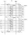
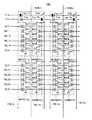
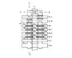
図1は本発明に係る第1実施例のNAND型不揮発性半導体記憶装置の構成例を示す図である。
【0050】
図1のNAND型不揮発性半導体記憶装置は、メモリアレイ10、ローデコーダ20、データラッチ回路群30、カラム選択部40、および昇圧回路50により構成されている。
【0051】
図1のNAND型不揮発性半導体記憶装置は、便宜上、2本の主ビット線、各主ビット線毎に階層化された2本の副ビット線、各副ビット線毎に接続された2本のNAND列からなるメモリアレイを有するものであるが、実際のメモリアレイにおいては、たとえば64Mビットのメモリの場合、主ビット線は512バイト(約4k本)、各主ビット線毎に階層化された副ビット線は16本、各副ビット線毎に接続されたNAND列は64本、各NAND列に直列接続されるメモリトランジスタの個数は16個程度である。
【0052】
メモリアレイ10において、MBLa、MBLbは主ビット線を示し、主ビット線MBLaは副ビット線SBLaおよびSBLa’に階層化され、主ビット線MBLbは副ビット線SBLbおよびSBLb’に階層化されている。
副ビット線SBLaは接続トランジスタTG1aを介して主ビット線MBLaに接続され、接続トランジスタTG2aを介してプリチャージ線PCLに接続される。
副ビット線SBLa’は接続トランジスタTG1a’を介して主ビット線MBLaに接続され、接続トランジスタTG2a’を介してプリチャージ線PCLに接続される。
副ビット線SBLbは接続トランジスタTG1bを介して主ビット線MBLbに接続され、接続トランジスタTG2bを介してプリチャージ線PCLに接続される。
副ビット線SBLb’は接続トランジスタTG1b’を介して主ビット線MBLbに接続され、接続トランジスタTG2b’を介してプリチャージ線PCLに接続される。
【0053】
接続トランジスタTG1a、TG1bは接続制御線TL1により制御され、接続トランジスタTG1a’、TG1b’は接続制御線TL1’により制御され、接続トランジスタTG2a、TG2bは接続制御線TL2により制御され、接続トランジスタTG2a’、TG2b’は接続制御線TL2’により制御される。
【0054】
副ビット線SBLaはNAND列NAND1aおよびNAND2aに接続され、副ビット線SBLa’はNAND列NAND1a’およびNAND2a’に接続され、副ビット線SBLbはNAND列NAND1bおよびNAND2bに接続され、副ビット線SBLb’はNAND列NAND1b’およびNAND2b’に接続される。
各NAND列は選択トランジスタおよびメモリトランジスタが直列接続されてなり、それぞれ選択ゲート線SL(SL’)およびワード線WL(WL’)により制御される。
主ビット線MBLaはデータラッチ回路SAaに接続され、主ビット線MBLbはデータラッチ回路SAbに接続されている。
【0055】
昇圧回路50は、データプログラム動作時に高電圧VPPおよび中間電圧VMを発生し、ローデコーダ20にプログラム電圧Vpgm(VPP)およびパス電圧Vpass(VM)を供給し、プリチャージ線PCLにプログラム禁止のプリチャージ電圧Vpc(VM)を供給する。
【0056】
図2は、図1のNAND型不揮発性半導体記憶装置において、メモリアレイ10の具体的構成を示す図であるが、便宜上、2本の主ビット線と、各主ビット線毎に1本の副ビット線のみが図示されている。
【0057】
図2において、主ビット線MBLaは副ビット線SBLaに階層化され、主ビット線MBLbは副ビット線SBLbに階層化されている。
副ビット線SBLaは接続トランジスタTG1aを介して主ビット線MBLaに接続され、接続トランジスタTG2aを介してプリチャージ線PCLに接続される。
副ビット線SBLbは接続トランジスタTG1bを介して主ビット線MBLbに接続され、接続トランジスタTG2bを介してプリチャージ線PCLに接続される。
接続トランジスタTG1a、TG1bは接続制御線TL1により制御され、接続トランジスタTG2a、TG2bは接続制御線TL2により制御される。
副ビット線SBLaにはNAND列NAND1aおよびNAND2aが接続され、副ビット線SBLbにはNAND列NAND1bおよびNAND2bが接続されている。
【0058】
各NAND列はそれぞれ2個の選択トランジスタST1,ST2、および4個のメモリトランジスタMT1〜MT4が直列接続されて構成されている。
NAND列NAND1aおよびNAND1bにおいて、選択トランジスタタST1は選択ゲート線SL11により制御され、選択トランジスタタST2は選択ゲート線SL12により制御され、またメモリトランジスタMT1〜MT4はそれぞれワード線WL11〜WL14により制御される。
NAND列NAND2aおよびNAND2bにおいて、選択トランジスタタST1は選択ゲート線SL21により制御され、選択トランジスタタST2は選択ゲート線SL22により制御され、またメモリトランジスタMT1〜MT4はそれぞれワード線WL21〜WL24により制御される。
なお、図2の構成においては、便宜上、NAND列1本に4個のメモリトランジスタが直列接続されているが、実際の構成においては、1本のNAND列に直列接続されるメモリトランジスタの個数は〜16個程度である。
【0059】
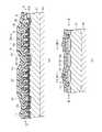
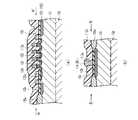
図3は図2のNAND型不揮発性半導体記憶装置のパターンレイアウト図である。
また、図4は図3のパターンレイアウト図におけるA−A’方向からの、デバイス構造断面図を示している。
【0060】
図3および図4において、100は半導体基板、101はメモリアレイ領域が形成されるP型ウェル領域、102はメモリトランジスタのソースおよびドレインN型拡散層、103はVSS配線およびビットコンタクト部のN型拡散層、104はトンネル酸化膜、105は選択トランジスタ部のゲート酸化膜、106はフローティングゲート電極をなす第1層目ポリシリコンゲート電極、107はONO−3層絶縁膜、108はメモリトランジスタおよび選択トランジスタの制御ゲート電極をなす第2層目ポリシリコン配線、109は第3層目ポリシリコン配線下の層間絶縁膜、110は第3層目ポリシリコン配線下のコンタクトホール、111は副ビット線およびプリチャージ線をなす3層目ポリシリコン配線、112はアルミニウム配線下の層間絶縁膜、113はアルミニウム配線下のコンタクトホール、および114は主ビット線をなすアルミニウム配線をそれぞれ示している。
【0061】
次に、図1および図2のNAND型不揮発性半導体記憶装置におけるデータプログラム動作について図5に関連付けて説明する。
図5は、ワード線WL12を選択してページプログラムをする場合に、NAND列NAND1a内のMT2がプログラムを禁止すべきメモリトランジスタであり、NAND列NAND1b内のMT2がプログラムすべきメモリトランジスタである場合の動作を説明するための図である。
【0062】
まず、接続制御線TL1に接地電圧GND(0V)が印加され副ビット線SBLaおよびSBLbが主ビット線MBLaおよびMBLbから切り離された状態で、接続制御線TL2にパス電圧Vpass(9V)が印加される。これにより、副ビット線SBLaおよびSBLbがプリチャージ線PCLからプログラム禁止のプリチャージ電圧(9V)に充電される。
同時に、選択ゲート線SL12に接地電圧GND(0V)が印加され、選択ゲート線SL11およびワード線WL11〜WL14にパス電圧Vpass(9V)が印加される。これにより、NAND列NAND1aおよびNAND1bのチャンネル部が副ビット線SBLaおよびSBLbを介してプログラム禁止電圧(9V)まで充電される。
このとき、非選択のNAND列NAND2aおよびNAND2bにおいては、選択ゲート線SL21,SL22およびワード線WL21〜WL24に接地電圧GND(0V)が印加されているので、当該NAND列は副ビット線と切り離され、メモリトランジスタには電圧が印加されていない状態である。
【0063】
次に、接続制御線TL2が接地電圧GND(0V)に立ち下げられて副ビット線SBLaおよびSBLbがプリチャージ線PCLから切り離された状態で、接続制御線TL1が電源電圧VCC(3.3V)に立ち上げられて副ビット線SBLaおよびSBLbが主ビット線MBLaおよびMBLbに接続される。
ここで、プログラムを禁止すべきメモリトランジスタ(NAND1a内のMT2)が接続された主ビット線MBLaは電源電圧VCC(3.3V)に、プログラムすべきメモリトランジスタ(NAND1b内のMT2)が接続された主ビット線MBLbは接地電圧GND(0V)に、それぞれ対応するデータラッチ回路を介して設定されている。
その結果、NAND列NAND1aのチャンネル部および副ビット線SBLaはフローティング状態のままプログラム禁止電位に保持されるが、NAND列NAND1bのチャンネル部および副ビット線SBLbのプログラム禁止電位は主ビット線MBLbに放電される。
同時に、選択ワード線WL12の印加電圧がプログラム電圧Vpgm(18V)に立ち上げられる。
その結果、NAND列NAND1a内のメモリトランジスタMT2はプログラム禁止電圧により消去状態に保持され、NAND列NAND1b内のメモリトランジスタMT2はプログラム電圧Vpgmによりデータプログラムがなされ、しきい値電圧は正方向にシフトして、たとえば消去状態の−3Vから2V程度になる。
【0064】
上述した図5の実施例は、従来の主ビット線を介して非選択NAND列チャンネル部の電位をプログラム禁止電位まで充電する方式に比較して、充電容量を大幅に減少させることができることから、低電圧動作に適しており、さらにデータラッチ回路のレイアウトも容易である。
また、ワード線印加電圧の容量カップリングによりNAND列チャンネル部の電位を上昇させる従来のセルフブースト動作と比較して、プログラム禁止電位を充分高い電圧値(〜9V)に設定することが可能である。
したがって、非選択メモリトランジスタに対するディスターブ耐性を向上させることができる。
【0065】
図6は、上述した図5に関連付けて説明した動作のタイミングチャートを示す図である。
以下、図5のデータプログラム動作を、図6のタイミングチャートを参照しながらさらに詳細に説明する。
【0066】
まず図6において、(a)に示すφP/Rはプログラム/ベリファイ制御信号であり、図中時刻t1〜t4の間は第1回目のプログラム/ベリファイ動作が行われ、また時刻t4〜t7の間は第2回目のプログラム/ベリファイ動作が行われる。
【0067】
まず、時刻t1で第1回目のプログラム動作が開始されて、図6(b),(d)に示すように、接続制御線TL1および選択ゲート線SL12に接地電圧GND(0V)が印加され、図6(c),(e)および(f)に示すように、接続制御線TL2および選択ゲート線SL11およびすべてのワード線WLにパス電圧Vpass(9V)が印加される。
その結果、図6(g),(h)に示すように、NAND列NAND1aのチャンネル部電位VCHaおよびNAND列NAND1bのチャンネル部電位VCHbは、副ビット線およびプリチャージ線を介してプログラム禁止電圧Vpc(9V)まで充電される。
【0068】
次に、図6(c),(b)に示すように、時刻t2で、接続制御線TL2が接地電圧GND(0V)に立ち下げされ、接続制御線TL1が電源電圧VCC(3.3V)に立ち上げられる。
その結果、図6(g),(h)に示すように、プログラムを禁止すべきメモリトランジスタが在するチャンネル部電位VCHaはフローティング状態のままプログラム禁止電位を保持するが、プログラムすべきメモリトランジスタが在するVCHbのプログラム禁止電位は主ビット線に放電されてGND(0V)になる。
一方、図6(e)に示すように、選択ワード線にはプログラム電圧Vpgm(18V)が印加され、時刻t2〜t3の間において、当該ワード線に接続されたメモリトランジスタ一括にページプログラムが行われる。
【0069】
次に時刻t3〜t4の間は、第1回目のベリファイ動作期間であり、図6(c),(e)に示すように、接続制御線TL2および選択ワード線にそれぞれ電源電圧VCCおよび接地電圧GNDが印加され、図6(b),(f),(d)に示すように、接続制御線TL1およびすべての非選択ワード線および選択ゲート線SL11およびSL12に電源電圧VCCが印加されてパス状態として、通常のNAND型フラッシュメモリと同様のベリファイ動作が行われる。
また、時刻t4〜t7の間は第2回目のプログラム/ベリファイ動作であり、第1回目のプログラム/ベリファイ動作のまったくの繰り返しである。
【0070】
図7は、図1〜図6の本発明の第1実施例のNAND型不揮発性半導体記憶装置において、すでに説明したプログラム動作、および消去動作、読み出し動作についての、各バイアス設定を示す図である。
なお図中、プログラム動作は便宜上プリチャージ時(図6において時刻t1〜t2)と実プログラム時(図6において時刻t2〜t3)に分けて示されている。
【0071】
図7において、プログラム動作はすでに説明したとおりであり、再度の説明を省略する。
消去動作については、従来のNAND型フラッシュメモリと基本的に同様であり、選択NAND列ブロックの全ワード線に0V、非選択NAND列ブロックの全ワード線およびメモリアレイの基板PWELLに高電圧(Verase=22V)が印加される。
その結果、選択NAND列ブロックのメモリトランジスタのみ、フローティングゲートから基板に電子が引き抜かれて、メモリトランジスタのしきい値電圧は負方向にシフトして、たとえば−3V程度になる。
読み出し動作についても、従来のNAND型フラッシュメモリと基本的に同様であり、選択NAND列ブロックにおいては、選択ワード線に接地電圧GNDが印加され、すべての非選択ワード線および選択ゲート線SLおよび接続制御線TL1に電源電圧VCCが印加されてパス状態として、通常のNAND型フラッシュメモリと同様の読み出し動作が行われる。
【0072】
以上説明したように、本第1実施例のNAND型不揮発性半導体記憶装置によれば、主ビット線が副ビット線に階層化されたメモリアレイ構成をなし、メモリトランジスタがプログラムを禁止すべきメモリトランジスタである場合、当該NAND列チャンネル部の電位を副ビット線を介してプログラム禁止電位まで充電する。
したがって、従来の主ビット線を介して非選択NAND列チャンネル部の電位をプログラム禁止電位まで充電する方式に比較して、充電容量を大幅に減少させることができることから低電圧動作に適し、さらにデータラッチ回路のレイアウトも容易となる。
また、ワード線印加電圧の容量カップリングによりNAND列チャンネル部の電位を上昇させるセルフブースト動作と比較して、プログラム禁止電位を充分高い電圧値に設定することが可能である。
そのために、データプログラム時のディスターブ耐性を向上させることができる。
【0073】
第2実施例
図8は本発明に係る第2実施例のNAND型不揮発性半導体記憶装置の構成例を示す図である。
本第2実施例が上記第1実施例と異なる点は、プリチャージ線を用いることなく、主ビット線から選択トランジスタを介してプログラム禁止電圧(9V)を副ビット線に供給した後、選択トランジスタのゲート電位を電源電圧VCCレベルに保持した状態で、選択された主ビット線は接地電圧GNDに設定し、非選択の主ビット線は電源電圧VCCに設定して、選択されなかった副ビット線をフローティング状態とするようにしたことにある。
【0074】
図8のNAND型不揮発性半導体記憶装置は、メモリアレイ10A、ローデコーダ20、データラッチ回路群30、カラム選択部40、および昇圧回路50により構成されている。
【0075】
図8のNAND型不揮発性半導体記憶装置は、便宜上、2本の主ビット線、各主ビット線毎に階層化された2本の副ビット線、各副ビット線毎に接続された2本のNAND列からなるメモリアレイを示す図であるが、実際のメモリアレイにおいては、たとえば64Mビットのメモリの場合、主ビット線は512バイト(約4k本)、各主ビット線毎に階層化された副ビット線は16本、各NAND列に直列接続されるメモリトランジスタの個数は16個程度である。
【0076】
メモリアレイ10Aにおいて、MBLa、MBLbは主ビット線を示し、主ビット線MBLaは副ビット線SBLaおよびSBLa’に階層化され、主ビット線MBLbは副ビット線SBLbおよびSBLb’に階層化されている。
副ビット線SBLaの一端側は接続トランジスタTG1aを介して主ビット線MBLaに接続され、副ビット線SBLa’は接続トランジスタTG1a’を介して主ビット線MBLaに接続される。
副ビット線SBLbは接続トランジスタTG1bを介して主ビット線MBLbに接続され、副ビット線SBLb’は接続トランジスタTG1b’を介して主ビット線MBLbに接続される。
【0077】
接続トランジスタTG1a、TG1bは接続制御線TL1により制御され、接続トランジスタTG1a’、TG1b’は接続制御線TL1’により制御される。
【0078】
副ビット線SBLaはNAND列NAND1aおよびNAND2aに接続され、副ビット線SBLa’はNAND列NAND1a’およびNAND2a’に接続され、副ビット線SBLbはNAND列NAND1bおよびNAND2bに接続され、副ビット線SBLb’はNAND列NAND1b’およびNAND2b’に接続される。
各NAND列は選択トランジスタおよびメモリトランジスタが直列接続されてなり、それぞれ選択ゲート線SL(SL’)およびワード線WL(WL’)により制御される。
主ビット線MBLaはデータラッチ回路SAaに接続され、主ビット線MBLbはデータラッチ回路SAbに接続されている。
【0079】
昇圧回路50は、データプログラム動作時に高電圧VPPおよび中間電圧VMを発生し、ローデコーダ20にプログラム電圧Vpgm(VPP)およびパス電圧Vpass(VM)を供給する。
【0080】
図9は、図8のNAND型不揮発性半導体記憶装置において、メモリアレイ10Aの具体的構成を示す図であるが、便宜上、2本の主ビット線と、各主ビット線毎に1本の副ビット線のみが図示されている。
【0081】
図9において、主ビット線MBLaは副ビット線SBLaに階層化され、主ビット線MBLbは副ビット線SBLbに階層化されている。
副ビット線SBLaは接続トランジスタTG1aを介して主ビット線MBLaに接続され、副ビット線SBLbは接続トランジスタTG1bを介して主ビット線MBLbに接続される。
接続トランジスタTG1a、TG1bは接続制御線TL1により制御される。副ビット線SBLaにはNAND列NAND1aおよびNAND2aが接続され、副ビット線SBLbにはNAND列NAND1bおよびNAND2bが接続されている。
【0082】
各NAND列はそれぞれ2個の選択トランジスタST1,ST2、および4個のメモリトランジスタMT1〜MT4が直列接続されて構成されている。
NAND列NAND1aおよびNAND1bにおいて、選択トランジスタタST1は選択ゲート線SL11により制御され、選択トランジスタタST2は選択ゲート線SL12により制御され、またメモリトランジスタMT1〜MT4はそれぞれワード線WL11〜WL14により制御される。
NAND列NAND2aおよびNAND2bにおいて、選択トランジスタタST1は選択ゲート線SL21により制御され、選択トランジスタタST2は選択ゲート線SL22により制御され、またメモリトランジスタMT1〜MT4はそれぞれワード線WL21〜WL24により制御される。
なお、図2の構成においては、便宜上、NAND列1本に4個のメモリトランジスタが直列接続されているが、実際の構成においては、1本のNAND列に直列接続されるメモリトランジスタの個数は〜16個程度である。
【0083】
図10は図9のNAND型不揮発性半導体記憶装置のパターンレイアウト図である。
また、図11は図10のパターンレイアウト図におけるA−A’方向からの、デバイス構造断面図を示している。
【0084】
図10および図11において、100は半導体基板、101はメモリアレイ領域が形成されるP型ウェル領域、102はメモリトランジスタのソースおよびドレインN型拡散層、103はVSS配線およびビットコンタクト部のN型拡散層、104はトンネル酸化膜、105は選択トランジスタ部のゲート酸化膜、106はフローティングゲート電極をなす第1層目ポリシリコンゲート電極、107はONO−3層絶縁膜、108はメモリトランジスタおよび選択トランジスタの制御ゲート電極をなす第2層目ポリシリコン配線、109は第3層目ポリシリコン配線下の層間絶縁膜、110は第3層目ポリシリコン配線下のコンタクトホール、111は副ビット線およびプリチャージ線をなす3層目ポリシリコン配線、112はアルミニウム配線下の層間絶縁膜、113はアルミニウム配線下のコンタクトホール、および114は主ビット線をなすアルミニウム配線をそれぞれ示している。
【0085】
次に、図8および図9のNAND型不揮発性半導体記憶装置におけるデータプログラム動作について図12に関連付けて説明する。
図12は、ワード線WL12を選択してページプログラムをする場合に、NAND列NAND1a内のMT2がプログラムを禁止すべきメモリトランジスタであり、NAND列NAND1b内のMT2がプログラムすべきメモリトランジスタである場合の動作を説明するための図である。
【0086】
まず、接続制御線TL1に接地電圧GND(0V)が印加され副ビット線SBLaおよびSBLbが主ビット線MBLaおよびMBLbから切り離された状態で、主ビット線MBLa,MBLbにパス電圧Vpass(9V)が印加される。この状態で接続制御線TL1にパス電圧Vpassが印加され、接続トランジスタTG1a,TG1bが導通状態に制御される。これにより、副ビット線SBLaおよびSBLbがプログラム禁止のパス電圧Vpass(9V)に充電される。
同時に、選択ゲート線SL12に接地電圧GND(0V)が印加され、選択ゲート線SL11およびワード線WL11〜WL14にパス電圧Vpass(9V)が印加される。
これにより、NAND列NAND1aおよびNAND1bのチャンネル部が副ビット線SBLaおよびSBLbを介してプログラム禁止電圧(9V)まで充電される。
このとき、非選択のNAND列NAND2aおよびNAND2bにおいては、選択ゲート線SL21,SL22およびワード線WL21〜WL24に接地電圧GND(0V)が印加されているので、当該NAND列は副ビット線と切り離され、メモリトランジスタには電圧が印加されていない状態である。
【0087】
次に、接続制御線TL1が電源電圧VCC(3.3V)に立ち下げられ、この状態で選択された側の主ビット線MBLbが接地電圧GND(0V)に立ち下げられ、選択されない側の主ビット線MBLaが電源電圧VCC(3.3V)に立ち下げられる。
これにより、接続トランジスタTG1bは接続状態に保持され、接続トランジスタTG1aはカットオフ状態となる。
その結果、NAND列NAND1aのチャンネル部および副ビット線SBLaはフローティング状態のままプログラム禁止電位に保持されるが、NAND列NAND1bのチャンネル部および副ビット線SBLbのプログラム禁止電位は主ビット線MBLbに放電される。
同時に、選択ワード線WL12の印加電圧がプログラム電圧Vpgm(18V)に立ち上げられる。
その結果、NAND列NAND1a内のメモリトランジスタMT2はプログラム禁止電圧により消去状態に保持され、NAND列NAND1b内のメモリトランジスタMT2はプログラム電圧Vpgmによりデータプログラムがなされ、しきい値電圧は正方向にシフトして、たとえば消去状態の−3Vから2V程度になる。
【0088】
上述した図12の実施例は、従来の主ビット線を介して非選択NAND列チャンネル部の電位をプログラム禁止電位まで充電する方式に比較して、低電圧動作に適しており、さらにデータラッチ回路のレイアウトも容易である。
また、ワード線印加電圧の容量カップリングによりNAND列チャンネル部の電位を上昇させる従来のセルフブースト動作と比較して、プログラム禁止電位を充分高い電圧値(〜9V)に設定することが可能である。
したがって、非選択メモリトランジスタに対するディスターブ耐性を向上させることができる。
【0089】
以上説明したように、本第2実施例のNAND型不揮発性半導体記憶装置によれば、上述した第1実施例と同様に、低電圧動作に適し、さらにデータラッチ回路のレイアウトも容易となる。
また、ワード線印加電圧の容量カップリングによりNAND列チャンネル部の電位を上昇させるセルフブースト動作と比較して、プログラム禁止電位を充分高い電圧値に設定することが可能である。
そのために、データプログラム時のディスターブ耐性を向上させることができる。
【0090】
第3実施例
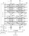
図13は本発明に係る第3実施例のNAND型不揮発性半導体記憶装置の構成例を示す図である。
図13の第3実施例の構成例が図1の第1実施例の構成例と異なる点は、主ビット線が対となって列方向に配線された第1副ビット線群および第2副ビット線群に階層化されたメモリアレイ構成をなしている点である。
したがって、主ビット線のカラム方向のピッチを緩和できるため、アルミニウム配線と拡散層とのビットコンタクトおよびデータラッチ回路のレイアウトがさらに容易となり、好適である。
【0091】
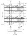
図13において、10Bはメモリアレイ、20はローデコーダ、30はデータラッチ回路、40はカラム選択部、および50は昇圧回路をそれぞれ示している。
図13のNAND型不揮発性半導体記憶装置は、便宜上、2本の主ビット線、各主ビット線毎に階層化された一対の副ビット線群、各副ビット線群を構成する2本の副ビット線、各副ビット線毎に接続された2本のNAND列からなるメモリアレイを示す図であるが、実際のメモリアレイにおいては、たとえば64Mビットのメモリの場合、主ビット線は256バイト(約2k本)、各副ビット線群を構成する副ビット線は16本、各副ビット線毎に接続されたNAND列は64本、各NAND列に直列接続されるメモリトランジスタの個数は16個程度である。
【0092】
メモリアレイ10Bにおいて、MBL1、MBL2は主ビット線を示し、主ビット線MBL1は副ビット線SBL1a、SBL1a’、および対となるSBL1b、SBL1b’に階層化され、主ビット線MBL2は副ビット線SBL2a、SBL2a’、および対となるSBL2b、SBL2b’に階層化されている。
副ビット線SBL1aは接続トランジスタTG11aを介して主ビット線MBL1に接続され、接続トランジスタTG12aを介してプリチャージ線PCLに接続される。
副ビット線SBL1a’は接続トランジスタTG11a’を介して主ビット線MBL1に接続され、接続トランジスタTG12a’を介してプリチャージ線PCLに接続される。
副ビット線SBL1bは接続トランジスタTG11bを介して主ビット線MBL1に接続され、接続トランジスタTG12bを介してプリチャージ線PCLに接続される。
副ビット線SBL1b’は接続トランジスタTG11b’を介して主ビット線MBL1に接続され、接続トランジスタTG12b’を介してプリチャージ線PCLに接続される。
【0093】
副ビット線SBL2aは接続トランジスタTG21aを介して主ビット線MBL2に接続され、接続トランジスタTG22aを介してプリチャージ線PCLに接続される。
副ビット線SBL2a’は接続トランジスタTG21a’を介して主ビット線MBL2に接続され、接続トランジスタTG22a’を介してプリチャージ線PCLに接続される。
副ビット線SBL2bは接続トランジスタTG21bを介して主ビット線MBL2に接続され、接続トランジスタTG22bを介してプリチャージ線PCLに接続される。
副ビット線SBL2b’は接続トランジスタTG21b’を介して主ビット線MBL2に接続され、接続トランジスタTG22b’を介してプリチャージ線PCLに接続される。
【0094】
接続トランジスタTG11a、TG21aは接続制御線TL1aにより制御され、接続トランジスタTG11b、TG21bは接続制御線TL1bにより制御され、接続トランジスタTG12a、TG22aは接続制御線TL2aにより制御され、接続トランジスタTG12b、TG22bは接続制御線TL2bにより制御され、接続トランジスタTG11a’、TG21a’は接続制御線TL1a’により制御され、接続トランジスタTG11b’、TG21b’は接続制御線TL1b’により制御され、接続トランジスタTG12a’、TG22a’は接続制御線TL2a’により制御され、接続トランジスタTG12b’、TG22b’は接続制御線TL2b’により制御される。
【0095】
副ビット線SBL1aはNAND列NAND11aおよびNAND12aに接続され、副ビット線SBL1bはNAND列NAND11bおよびNAND12bに接続され、副ビット線SBL2aはNAND列NAND21aおよびNAND22aに接続され、副ビット線SBL2bはNAND列NAND21bおよびNAND22bに接続され、副ビット線SBL1a’はNAND列NAND11a’およびNAND12a’に接続され、副ビット線SBL1b’はNAND列NAND11b’およびNAND12b’に接続され、副ビット線SBL2a’はNAND列NAND21a’およびNAND22a’に接続され、副ビット線SBL2b’はNAND列NAND21b’およびNAND22b’に接続される。
【0096】
各NAND列は選択トランジスタおよびメモリトランジスタが直列接続されてなり、それぞれ選択ゲート線SL(SL’)およびワード線WL(WL’)により制御される。
主ビット線MBL1はデータラッチ回路SA1に接続され、主ビット線MBL2はデータラッチ回路SA2に接続されている。
【0097】
50の昇圧回路は、データプログラム動作時に高電圧VPPおよび中間電圧VMを発生し、ローデコーダ20にプログラム電圧Vpgm(VPP)およびパス電圧Vpass(VM)を供給し、プリチャージ線PCLにプログラム禁止のプリチャージ電圧Vpc(VM)を供給する。
【0098】
図14は、図13のNAND型不揮発性半導体記憶装置において、メモリアレイ10Bの具体的構成を示す図であるが、便宜上、2本の主ビット線と、各主ビット線毎に1対の副ビット線のみが図示されている。
【0099】
図14において、主ビット線MBL1は対となる副ビット線SBL1aおよびSBL1bに階層化され、主ビット線MBL2は対となる副ビット線SBL2aおよびSBL2bに階層化されている。
副ビット線SBL1aは直列接続された接続トランジスタTG11aおよびパストランジスタPass−TRを介して主ビット線MBL1に接続され、接続トランジスタTG12aおよびパストランジスタPass−TRを介してプリチャージ線PCLに接続される。
副ビット線SBL1bは直列接続された接続トランジスタTG11bおよびパストランジスタPass−TRを介して主ビット線MBL1に接続され、接続トランジスタTG12bおよびパストランジスタPass−TRを介してプリチャージ線PCLに接続される。
副ビット線SBL2aは直列接続された接続トランジスタTG21aおよびパストランジスタPass−TRを介して主ビット線MBL2に接続され、接続トランジスタTG22aおよびパストランジスタPass−TRを介してプリチャージ線PCLに接続される。
副ビット線SBL2bは直列接続された接続トランジスタTG21bおよびパストランジスタPass−TRを介して主ビット線MBL2に接続され、接続トランジスタTG22bおよびパストランジスタPass−TRを介してプリチャージ線PCLに接続される。
【0100】
接続トランジスタTG11a、TG21aは接続制御線TL1aにより制御され、接続トランジスタTG11b、TG21bは接続制御線TL1bにより制御され、接続トランジスタTG12a、TG22aは接続制御線TL2aにより制御され、接続トランジスタTG12b、TG22bは接続制御線TL2bにより制御される。
各接続トランジスタに直列接続されるパストランジスタPass−TRは、チャンネル部にリン等のN型不純物層が形成されており、接続制御線に印加する電圧にかかわらず常にオン状態となる。
副ビット線SBL1aはNAND列NAND11aおよびNAND12aに接続され、副ビット線SBL1bはNAND列NAND11bおよびNAND12bに接続され、副ビット線SBL2aはNAND列NAND21aおよびNAND22aに接続され、副ビット線SBL2bはNAND列NAND21bおよびNAND22bに接続される。
【0101】
各NAND列はそれぞれ2個の選択トランジスタST1,ST2、および4個のメモリトランジスタMT1〜MT4が直列接続されて構成されている。
NAND列NAND11a、NAND11b、NAND21aおよびNAND21bにおいて、選択トランジスタタST1は選択ゲート線SL11により制御され、選択トランジスタタST2は選択ゲート線SL12により制御され、またメモリトランジスタMT1〜MT4はそれぞれワード線WL11〜WL14により制御される。
また、NAND列NAND12a、NAND12b、NAND22aおよびNAND22bにおいて、選択トランジスタタST1は選択ゲート線SL21により制御され、選択トランジスタタST2は選択ゲート線SL22により制御され、またメモリトランジスタMT1〜MT4はそれぞれワード線WL21〜WL24により制御される。
なお、図13の構成においては、便宜上、NAND列1本に4個のメモリトランジスタが直列接続されているが、実際の構成においては、1本のNAND列に直列接続されるメモリトランジスタの個数は〜16個程度である。
【0102】
図15は図14のNAND型不揮発性半導体記憶装置のパターンレイアウト図である。
また、図16(a),(b)はデバイス構造断面図であり、図16(a)は図15におけるA−A’線方向からの、図16(b)はB−B’線方向からの断面図を示している。
【0103】
図15および図16(a),(b)において、100は半導体基板、101はメモリアレイ領域が形成されるP型ウェル領域、102はメモリトランジスタのソースおよびドレインN型拡散層、103はVSS配線およびビットコンタクト部のN型拡散層、103aはパストランジスタのチャンネル部に形成されたN型拡散層、104はトンネル酸化膜、105は選択トランジスタ部のゲート酸化膜、105aはLOCOS素子分離酸化膜、106はフローティングゲート電極をなす第1層目ポリシリコンゲート電極、107はONO−3層絶縁膜、108はメモリトランジスタおよび選択トランジスタの制御ゲート電極をなす第2層目ポリシリコン配線、109は第3層目ポリシリコン配線下の層間絶縁膜、110は第3層目ポリシリコン配線下のコンタクトホール、111は副ビット線およびプリチャージ線をなす3層目ポリシリコン配線、112はアルミニウム配線下の層間絶縁膜、113はアルミニウム配線下のコンタクトホール、および114は主ビット線をなすアルミニウム配線をそれぞれ示している。
【0104】
次に、図13および図14のNAND型不揮発性半導体記憶装置におけるデータプログラム動作について図17に関連付けて説明する。
図17は、ワード線WL12を選択してページプログラムを行い、かつ副ビット線SBL1aおよびSBL2aを選択して副ビット線SBL1bおよびSBL2bを選択しない場合に、NAND列NAND11a内のMT2がプログラムを禁止すべきメモリトランジスタであり、NAND列NAND21a内のMT2がプログラムすべきメモリトランジスタである場合の動作を説明するための図である。
この場合、ワード線WL12に接続されたメモリトランジスタにおいて、NAND列NAND21a内のメモリトランジスタMT2のみデータプログラムを行い、その他のNAND列NAND11a、NAND11bおよびNAND21b内のメモリトランジスタMT2はすべてデータプログラムを禁止する必要がある。
【0105】
まず、接続制御線TL1aおよびTL1bに接地電圧GND(0V)が印加され副ビット線SBL1a、SBL1b、SBL2aおよびSBL2bがすべて対応する主ビット線MBL1およびMBL2から切り離された状態で、接続制御線TL2aおよびTL2bにパス電圧Vpass(9V)が印加される。これにより、副ビット線SBL1a、SBL1b、SBL2aおよびSBL2bがプリチャージ線PCLからすべてプログラム禁止のプリチャージ電圧(9V)に充電される。
同時に、選択ゲート線SL12に接地電圧GND(0V)が印加され、選択ゲート線SL11およびワード線WL11〜WL14にパス電圧Vpass(9V)が印加される。これにより、NAND列NAND11a、NAND11b、NAND21aおよびNAND21bのチャンネル部がすべて副ビット線を介してプログラム禁止電圧(9V)まで充電される。
このとき、非選択ブロックのNAND列NAND12a、NAND12b、NAND22aおよびNAND22bにおいては、選択ゲート線SL21,SL22およびワード線WL21〜WL24に接地電圧GND(0V)が印加されているので、当該NAND列は副ビット線と切り離され、メモリトランジスタには電圧が印加されていない状態である。
【0106】
次に、接続制御線TL2aおよびTL2bが接地電圧GND(0V)に立ち下げられて副ビット線SBL1a、SBL1b、SBL2aおよびSBL2bがすべてプリチャージ線PCLから切り離された状態で、接続制御線TL1aが電源電圧VCC(3.3V)に立ち上げられて副ビット線SBL1aおよびSBL2aが主ビット線MBL1およびMBL2に接続される。
ここで、プログラムを禁止すべきメモリトランジスタ(NAND11a内のMT2)が接続された主ビット線MBL1は電源電圧VCCVCC(3.3V)に、プログラムすべきメモリトランジスタ(NAND21a内のMT2)が接続された主ビット線MBL2は接地電圧GND(0V)に、それぞれ対応するデータラッチ回路を介して設定されている。
その結果、NAND列NAND11a、NAND11bおよびNAND21bのチャンネル部および対応する副ビット線はフローティング状態のままプログラム禁止電位に保持されるが、NAND列NAND21aのチャンネル部および副ビット線SBL2aのプログラム禁止電位は主ビット線MBL2に放電される。
同時に、選択ワード線WL12の印加電圧がプログラム電圧Vpgm(18V)に立ち上げられる。
その結果、NAND列NAND11a、NAND11bおよびNAND21b内のメモリトランジスタMT2はプログラム禁止電圧により消去状態に保持され、NAND列NAND21a内のメモリトランジスタMT2はプログラム電圧Vpgmによりデータプログラムがなされ、しきい値電圧は正方向にシフトして、たとえば消去状態の−3Vから2V程度になる。
【0107】
上述した図17の実施例は、従来の主ビット線を介して非選択NAND列チャンネル部の電位をプログラム禁止電位まで充電する方式に比較して、充電容量を大幅に減少させることができることから低電圧動作に適するだけでなく、さらに主ビット線のカラム方向のピッチを緩和できるため、アルミニウム配線と拡散層とのビットコンタタクトおよびデータラッチ回路のレイアウトが容易となる。
また、ワード線印加電圧の容量カップリングによりNAND列チャンネル部の電位を上昇させる従来のセルフブースト動作と比較して、プログラム禁止電位を充分高い電圧値(〜9V)に設定することが可能である。
したがって、非選択メモリトランジスタに対するディスターブ耐性を向上させることができる。
【0108】
図18は、上述した図17に関連付けて説明した動作のタイミングチャートを示す図である。
以下、図17のデータプログラム動作を、図18のタイミングチャートを参照しながさらに詳細に説明する。
【0109】
まず図18において、(a)に示すφP/Rはプログラム/ベリファイ制御信号であり、図中時刻t1〜t4の間は第1回目のプログラム/ベリファイ動作が行われ、また時刻t4〜t7の間は第2回目のプログラム/ベリファイ動作が行われる。
【0110】
まず時刻t1で第1回目のプログラム動作が開始されて、図18(b)および(e)に示すように、接続制御線TL1aおよびTL1bおよび選択ゲート線SL12に接地電圧GND(0V)が印加され、図18(c),(d)および(f)に示すように、接続制御線TL2aおよびTL2bおよび選択ゲート線SL11およびすべてのワード線WLにパス電圧Vpass(9V)が印加される。
その結果、図18(h)に示すように、NAND列NAND11aのチャンネル部電位VCH11aおよびNAND11bのチャンネル部電位VCH11bおよびNAND21aのチャンネル部電位VCH21aおよびNAND21bのチャンネル部電位VCH21bは、すべて対応する副ビット線およびプリチャージ線を介してプログラム禁止電圧(9V)まで充電される。
【0111】
次に、図18(b),(c)に示すように、時刻t2で、接続制御線TL2aおよびTL2bが接地電圧GND(0V)に立ち下げられ、接続制御線TL1aが電源電圧VCC(3.3V)に立ち上げられる。
その結果、プログラムを禁止すべきメモリトランジスタが在するチャンネル部電位VCH11a、VCH11bおよびVCH21bはフローティング状態のままプログラム禁止電位を保持するが、プログラムすべきメモリトランジスタが在するVCH21aのプログラム禁止電位は主ビット線に放電されてGND(0V)になる。
一方、図18(f)に示すように、選択ワード線にはプログラム電圧Vpgm(18V)が印加され、時刻t2〜t3の間において、当該ワード線に接続されたメモリトランジスタ一括にページプログラムが行われる。
【0112】
次に時刻t3〜t4の間は、第1回目のベリファイ動作期間であり、図18(d),(f)に示すように、接続制御線TL1b、TL2b並びに選択ワード線WLに接地電圧GNDが印加され、図18(b),(g)および(e)に示すように、接続制御線TL1aおよびすべての非選択ワード線および選択ゲート線SL11およびSL12に電源電圧VCCが印加されてパス状態として、選択する一方の副ビット線側のみ通常のNAND型フラッシュメモリと同様のベリファイ動作が行われる。
また、時刻t4〜t7の間は第2回目のプログラム/ベリファイ動作であり、第1回目のプログラム/ベリファイ動作のまったくの繰り返しである。
【0113】
図19は、図13〜図18の本第3実施例のNAND型不揮発性半導体記憶装置において、すでに説明したプログラム動作、および消去動作、読み出し動作についての、各バイアス設定を示す図である。
なお図中、プログラム動作は便宜上プリチャージ時(図18において時刻t1〜t2)と実プログラム時(図18において時刻t2〜t3)に分けて示されている。
【0114】
図19において、プログラム動作はすでに説明したとおりであり、再度の説明を省略する。
消去動作については、従来のNAND型フラッシュメモリと基本的に同様であり、選択NAND列ブロックの全ワード線に0V、非選択NAND列ブロックの全ワード線およびメモリアレイの基板PWELLに高電圧(Verase=22V)が印加される。
その結果、選択NAND列ブロックのメモリトランジスタのみ、フローティングゲートから基板に電子が引き抜かれて、メモリトランジスタのしきい値電圧は負方向にシフトして、たとえば−3V程度になる。
読み出し動作についても、従来のNAND型フラッシュメモリと基本的に同様であり、選択NAND列ブロックにおいては、選択ワード線に接地電圧GNDが印加され、すべての非選択ワード線および選択ゲート線SLおよび選択接続制御線TL1aに電源電圧VCCが印加されてパス状態として、通常のNAND型フラッシュメモリと同様の読み出し動作が行われる。
【0115】
以上説明したように、本第3実施例のNAND型不揮発性半導体記憶装置によれば、主ビット線が対となって列方向に配線された第1副ビット線群および第2副ビット線群に階層化されたメモリアレイ構成をなし、非選択側の副ビット線から充電したNAND列チャンネル部のプログラム禁止電位を保持したまま、選択側の副ビット線から充電したNAND列に対して選択的にページプログラムを行う。
したがって、従来の主ビット線を介して非選択NAND列チャンネル部の電位をプログラム禁止電位まで充電する方式に比較して、充電容量を大幅に減少させることができることから低電圧動作に適するだけでなく、さらに主ビット線のカラム方向のピッチを緩和できるため、アルミニウム配線と拡散層とのビットコンタクトおよびデータラッチ回路のレイアウトも容易となる。
また、ワード線印加電圧の容量カップリングによりNAND列チャンネル部の電位を上昇させるセルフブースト動作と比較して、プログラム禁止電位を充分高い電圧値に設定することが可能である。
そのために、データプログラム時のディスターブ耐性を向上させることができる。
【0116】
第4実施例
図20は本発明に係る第4実施例のNAND型不揮発性半導体記憶装置の構成例を示す図である。
【0117】
図20のNAND型不揮発性半導体記憶装置は、メモリアレイ10C、ローデコーダ20、データラッチ回路群30、およびカラム選択部40により構成されている。
図20のNAND型不揮発性半導体記憶装置は、便宜上、2本の主ビット線、各主ビット線毎に階層化された一対の副ビット線群、各副ビット線群を構成する2本の副ビット線、各副ビット線毎に接続された2本のNAND列からなるメモリアレイを示す図であるが、実際のメモリアレイにおいては、例えば64Mビットのメモリの場合、主ビット線は256バイト(約2k本)、各副ビット線群を構成する副ビット線は16本、各副ビット線毎に接続されたNAND列は64本、各NAND列に直列接続されるメモリトランジスタの個数は16個程度である。
【0118】
メモリアレイ10Cにおいて、MBL1、MBL2は主ビット線を示し、主ビット線MBL1は副ビット線SBL1a、SBL1a’、および対となるSBL1b、SBL1b’に階層化され、主ビット線MBL2は副ビット線SBL2a、SBL2a’、および対となるSBL2b、SBL2b’に階層化されている。
副ビット線SBL1aは接続トランジスタTG1aを介して主ビット線MBL1に接続される。
副ビット線SBL1a’は接続トランジスタTG1a’を介して主ビット線MBL1に接続される。
副ビット線SBL1bは接続トランジスタTG1bを介して主ビット線MBL1に接続される。
副ビット線SBL1b’は接続トランジスタTG1b’を介して主ビット線MBL1に接続される。
副ビット線SBL2aは接続トランジスタTG2aを介して主ビット線MBL2に接続される。
副ビット線SBL2a’は接続トランジスタTG2a’を介して主ビット線MBL2に接続される。
副ビット線SBL2bは接続トランジスタTG2bを介して主ビット線MBL2に接続される。
副ビット線SBL2b’は接続トランジスタTG2b’を介して主ビット線MBL2に接続される。
【0119】
接続トランジスタTG1a、TG2aは接続制御線TL1aにより制御され、接続トランジスタTG1b、TG2bは接続制御線TL1bにより制御され、接続トランジスタTG1a’、TG2a’は接続制御線TL1a’により制御され、接続トランジスタTG1b’、TG2b’は接続制御線TL1b’により制御される。
副ビット線SBL1aはNAND列NAND11aおよびNAND12aに接続され、副ビット線SBL1bはNAND列NAND11bおよびNAND12bに接続され、副ビット線SBL2aはNAND列NAND21aおよびNAND22aに接続され、副ビット線SBL2bはNAND列NAND21bおよびNAND22bに接続され、副ビット線SBL1a’はNAND列NAND11a’およびNAND12a’に接続され、副ビット線SBL1b’はNAND列NAND11b’およびNAND12b’に接続され、副ビット線SBL2a’はNAND列NAND21a’およびNAND22a’に接続され、副ビット線SBL2b’はNAND列NAND21b’およびNAND22b’に接続される。
各NAND列は選択トランジスタおよびメモリトランジスタが直列接続されてなり、それぞれ選択ゲート線SL(SL’)およびワード線WL(WL’)に制御される。
主ビット線MBL1はデータラッチ回路SA1に接続、主ビット線MBL2はデータラッチ回路SA2に接続されている。
【0120】
図21は、図20のNAND型不揮発性半導体記憶装置において、メモリアレイ10Cの具体的構成を示す図であるが、便宜上、2本の主ビット線と、各主ビット線毎に1対の副ビット線のみが図示されている。
【0121】
図21において、主ビット線MBL1は対となる副ビット線SBL1aおよびSBL1bに階層化され、主ビット線MBL2は対となる副ビット線SBL2aおよびSBL2bに階層化されている。
副ビット線SBL1aは接続トランジスタTG1aおよびパストランジスタPass−TRを介して主ビット線MBL1に接続される。
副ビット線SBL1bは接続トランジスタTG1bおよびパストランジスタPass−TRを介して主ビット線MBL1に接続される。
副ビット線SBL2aは接続トランジスタTG2aおよびパストランジスタPass−TRを介して主ビット線MBL2に接続される。
副ビット線SBL2bは接続トランジスタTG2bおよびパストランジスタPass−TRを介して主ビット線MBL2に接続される。
【0122】
接続トランジスタTG1a、TG2aは接続制御線TL1aにより制御され、接続トランジスタTG1b、TG2bは接続制御線TL1bにより制御される。
各接続トランジスタに直列接続されるパストランジスタPass−TRは、チャンネル部にリン等のN型不純物層が形成されており、接続制御線に印加する電圧に係らず常にオン状態となる。
したがって、図21のメモリアレイにおいては、接続制御線TL1aがハイレベルであり、接続制御線TL1bがローレベルである場合には、副ビット線SBL1aが主ビット線MBL1に接続され、副ビット線SBL2aが主ビット線MBL2に接続される。
また、接続制御線TL1bがハイレベルであり、接続制御線TL1aがローレベルである場合には、副ビット線SBL1bが主ビット線MBL1に接続され、副ビット線SBL2bが主ビット線MBL2に接続される。
副ビット線SBL1aはNAND列NAND11aおよびNAND12aに接続され、副ビット線SBL1bはNAND列NAND11bおよびNAND12bに接続され、副ビット線SBL2aはNAND列NAND21aおよびNAND22aに接続され、副ビット線SBL2bはNAND列NAND21bおよびNAND22bに接続される。
【0123】
各NAND列はそれぞれ2個の選択トランジスタST1,ST2、およびび4個のメモリトランジスタMT1〜MT4が直列接続されて構成される。
NAND列NAND11a、NAND11b、NAND21aおよびNAND21bにおいて、選択トランジスタタST1は選択ゲート線SL11により制御され、選択トランジスタタST2は選択ゲート線SL12により制御され、またメモリトランジスタMT1〜MT4はそれぞれワード線WL11〜WL14により制御される。
NAND列NAND12a、NAND12b、NAND22aおよびNAND22bにおいて、選択トランジスタタST1は選択ゲート線SL21により制御され、選択トランジスタタST2は選択ゲート線SL22により制御され、またメモリトランジスタMT1〜MT4はそれぞれワード線WL21〜WL24により制御される。
なお、図21の構成においては、便宜上、NAND列1本に4個のメモリトランジスタが直列接続されているが、実際の構成においては、1本のNAND列に直列接続されるメモリトランジスタの個数は〜16個程度である。
【0124】
図22は図21のNAND型不揮発性半導体記憶装置のパターンレイアウト図である。
また、図23(a)〜(b)はデバイス構造断面図であり、図23(a)はA−A’方向からの、図23(b)はB−B’方向からの断面図を示している。
【0125】
図22および図23(a),(b)において、100は半導体基板、101はメモリアレイ領域が形成されるP型ウェル領域、102はメモリトランジスタのソースおよびドレインN型拡散層、103はVSS配線およびビットコンタクト部のN型拡散層、103aはパストランジスタのチャンネル部に形成されたN型拡散層、104はトンネル酸化膜、105は選択トランジスタ部のゲート酸化膜、105aはLOCOS素子分離酸化膜、106はフローティングゲート電極をなす第1層目ポリシリコンゲート電極、107はONO−3層絶縁膜、108はメモリトランジスタおよび選択トランジスタの制御ゲート電極をなす第2層目ポリシリコン配線、109は第3層目ポリシリコン配線下の層間絶縁膜、110は第3層目ポリシリコン配線下のコンタクトホール、111は副ビット線をなす3層目ポリシリコン配線、112はアルミニウム配線下の層間絶縁膜、113はアルミニウム配線下のコンタクトホール、114は主ビット線をなすアルミニウム配線をそれぞれ示している。
【0126】
図22のパターンレイアウト図において、副ビット線をなす第3層目ポリシリコン配線(111)および当該副ビット線とのビットコンタクト(110)のカラム方向のピッチは、従来のビット線ピッチに比して緩和されていない。
しかし、ポリシリコン配線およびコンタクトのプロセス上の微細加工は、アルミニウム配線およびコンタクトのプロセス上の微細加工よりも容易であるため、従来のビット線構成よりもセルサイズのシュリンクに有利である。
【0127】
以上説明したように、本第4実施例のNAND型不揮発性半導体記憶装置によれば、主ビット線が複数の列方向に複数群の副ビット線群に階層化されたメモリアレイ構成をなしている。
したがって、主ビット線のカラム方向のピッチを緩和できるため、アルミニウム配線と拡散層とのビットコンタクトおよびデータラッチ回路のレイアウトが容易となる。
【0128】
第5実施例
図24は本発明に係る第5実施例のNAND型不揮発性半導体記憶装置の構成例を示す図である。
図24の第5実施例の構成例が図20の第4実施例の構成例と異なる点は、対となって列方向に配線された副ビット線対が、それぞれ反対側の端部で接続トランジスタを介して主ビット線に接続されるメモリアレイ構成をなしている点である。
したがって、第4実施例において必要であったパストランジスタPass−TRが不要となり、プロセス工程(103aのN型拡散層)が削減でき、好適である。
【0129】
図24のNAND型不揮発性半導体記憶装置は、メモリアレイ10D、ローデコーダ20、データラッチ回路群30、およびカラム選択部40により構成されている。
図24のNAND型不揮発性半導体記憶装置は、便宜上、2本の主ビット線、各主ビット線毎に階層化された一対の副ビット線群、各副ビット線群を構成する2本の副ビット線、各副ビット線毎に接続された2本のNAND列からなるメモリアレイを示す図であるが、実際のメモリアレイにおいては、例えば64Mビットのメモリの場合、主ビット線は256バイト(約2k本)、各副ビット線群を構成する副ビット線は16本、各副ビット線毎に接続されたNAND列は64本、各NAND列に直列接続されるメモリトランジスタの個数は16個程度である。
【0130】
メモリアレイ10Dにおいて、MBL1、MBL2は主ビット線を示し、主ビット線MBL1は副ビット線SBL1a、SBL1a’、および対となるSBL1b、SBL1b’に階層化され、主ビット線MBL2は副ビット線SBL2a、SBL2a’、および対となるSBL2b、SBL2b’に階層化されている。
副ビット線SBL1aは接続トランジスタTG1aを介して主ビット線MBL1に接続される。
副ビット線SBL1a’は接続トランジスタTG1a’を介して主ビット線MBL1に接続される。
副ビット線SBL1bは接続トランジスタTG1bを介して主ビット線MBL1に接続される。
副ビット線SBL1b’は接続トランジスタTG1b’を介して主ビット線MBL1に接続される。
副ビット線SBL2aは接続トランジスタTG2aを介して主ビット線MBL2に接続される。
副ビット線SBL2a’は接続トランジスタTG2a’を介して主ビット線MBL2に接続される。
副ビット線SBL2bは接続トランジスタTG2bを介して主ビット線MBL2に接続される。
副ビット線SBL2b’は接続トランジスタTG2b’を介して主ビット線MBL2に接続される。
【0131】
接続トランジスタTG1a、TG2aは接続制御線TL1aにより制御され、接続トランジスタTG1b、TG2bは接続制御線TL1bにより制御され、接続トランジスタTG1a’、TG2a’は接続制御線TL1a’により制御され、接続トランジスタTG1b’、TG2b’は接続制御線TL1b’により制御される。
副ビット線SBL1aはNAND列NAND11aおよびNAND12aに接続され、副ビット線SBL1bはNAND列NAND11bおよびNAND12bに接続され、副ビット線SBL2aはNAND列NAND21aおよびNAND22aに接続され、副ビット線SBL2bはNAND列NAND21bおよびNAND22bに接続され、副ビット線SBL1a’はNAND列NAND11a’およびNAND12a’に接続され、副ビット線SBL1b’はNAND列NAND11b’およびNAND12b’に接続され、副ビット線SBL2a’はNAND列NAND21a’およびNAND22a’に接続され、副ビット線SBL2b’はNAND列NAND21b’およびNAND22b’に接続される。
各NAND列は選択トランジスタおよびメモリトランジスタが直列接続されてなり、それぞれ選択ゲート線SL(SL’)およびワード線WL(WL’)に制御される。
主ビット線MBL1はデータラッチ回路SA1に接続され、主ビット線MBL2はデータラッチ回路SA2に接続されている。
【0132】
図25は、図24のNAND型不揮発性半導体記憶装置において、メモリアレイ10Dの具体的構成を示す図であるが、便宜上、2本の主ビット線と、各主ビット線毎に1対の副ビット線のみが図示されている。
【0133】
図25において、主ビット線MBL1は対となる副ビット線SBL1aおよびSBL1bに階層化され、主ビット線MBL2は対となる副ビット線SBL2aおよびSBL2bに階層化されている。
副ビット線SBL1aは接続トランジスタTG1aを介して主ビット線MBL1に接続される。
副ビット線SBL1bは接続トランジスタTG1bを介して主ビット線MBL1に接続される。
副ビット線SBL2aは接続トランジスタTG2aを介して主ビット線MBL2に接続される。
副ビット線SBL2bは接続トランジスタTG2bを介して主ビット線MBL2に接続されれる。
【0134】
接続トランジスタTG1a、TG2aは接続制御線TL1aにより制御され、接続トランジスタTG1b、TG2bは接続制御線TL1bにより制御される。
図25のメモリアレイにおいては、接続制御線TL1aがハイレベルであり、接続制御線TL1bがローレベルである場合には、副ビット線SBL1aが主ビット線MBL1に接続され、副ビット線SBL2aが主ビット線MBL2に接続される。
また、接続制御線TL1bがハイレベルであり、接続制御線TL1aがローレベルである場合には、副ビット線SBL1bが主ビット線MBL1に接続され、副ビット線SBL2bが主ビット線MBL2に接続される。
副ビット線SBL1aはNAND列NAND11aおよびNAND12aに接続され、副ビット線SBL1bはNAND列NAND11bおよびNAND12bに接続され、副ビット線SBL2aはNAND列NAND21aおよびNAND22aに接続され、副ビット線SBL2bはNAND列NAND21bおよびNAND22bに接続される。
【0135】
各NAND列はそれぞれ2個の選択トランジスタST1,ST2、およびび4個のメモリトランジスタMT1〜MT4が直列接続されて構成されている。
NAND列NAND11a、NAND11b、NAND21aおよびNAND21bにおいて、選択トランジスタタST1は選択ゲート線SL11により制御され、選択トランジスタタST2は選択ゲート線SL12により制御され、またメモリトランジスタMT1〜MT4はそれぞれワード線WL11〜WL14により制御される。
NAND列NAND12aおよびNAND12bおよびNAND22aおよびNAND22bにおいて、選択トランジスタタST1は選択ゲート線SL21により制御され、選択トランジスタタST2は選択ゲート線SL22により制御され、またメモリトランジスタMT1〜MT4はそれぞれワード線WL21〜WL24により制御される。
なお、図25の構成においては、便宜上、NAND列1本に4個のメモリトランジスタが直列接続されているが、実際の構成においては、1本のNAND列に直列接続されるメモリトランジスタの個数は〜16個程度である。
【0136】
図26は図25のNAND型不揮発性半導体記憶装置のパターンレイアウト図である。
また、図27(a),(b)はデバイス構造断面図であり、図27(a)はA−A’方向からの、図27(b)はB−B’方向からの断面図を示している。
【0137】
図26および図27(a),(b)において、100は半導体基板、101はメモリアレイ領域が形成されるP型ウェル領域、102はメモリトランジスタのソースおよびドレインN型拡散層、103はVSS配線およびビットコンタクト部のN型拡散層、104はトンネル酸化膜、105は選択トランジスタ部のゲート酸化膜、105aはLOCOS素子分離酸化膜、106はフローティングゲート電極をなす第1層目ポリシリコンゲート電極、107はONO−3層絶縁膜、108はメモリトランジスタおよび選択トランジスタの制御ゲート電極をなす第2層目ポリシリコン配線、109は第3層目ポリシリコン配線下の層間絶縁膜、110は第3層目ポリシリコン配線下のコンタクトホール、111は副ビット線をなす3層目ポリシリコン配 線、112はアルミニウム配線下の層間絶縁膜、113はアルミニウム配線下のコンタクトホール、114は主ビット線をなすアルミニウム配線をそれぞれ示している。
【0138】
図26のパターンレイアウト図において、副ビット線をなす第3層目ポリシリコン配線(111)および当該副ビット線とのビットコンタクト(110)のカラム方向のピッチは、従来のビット線ピッチに比して緩和されていない。
しかし、ポリシリコン配線およびコンタクトのプロセス上の微細加工は、アルミニウム配線およびコンタクトのプロセス上の微細加工よりも容易であるため、従来のビット線構成よりもセルサイズのシュリンクに有利である。
【0139】
以上説明したように、本第4実施例のNAND型不揮発性半導体記憶装置によれば、主ビット線が複数の列方向に複数群の副ビット線群に階層化されたメモリアレイ構成をなしている。
したがって、主ビット線のカラム方向のピッチを緩和できるため、アルミニウム配線と拡散層とのビットコンタクトおよびデータラッチ回路のレイアウトが容易となる。
またすでに説明した第4実施例と比較して、プロセス工程が削減でき、好適である。
【0140】
【発明の効果】
以上説明したように、本発明によれば、低電圧での単一電源動作に適し、ビット線毎のデータラッチ回路のレイアウトが容易で、しかもディスターブ耐性の良好なデータプログラム動作を行うNAND型不揮発性半導体記憶装置を実現することができる。
さらに、本発明によれば、実質的にメモリセルサイズを大きくすることなく、ビット線レイアウトのカラム方向のピッチを緩和できるNAND型不揮発性半導体記憶装置を実現することができる。
【図面の簡単な説明】
【図1】本発明に係る第1実施例のNAND型不揮発性半導体記憶装置の構成例を示す図である。
【図2】図1におけるメモリアレイの具体的構成を示す図である。
【図3】図2のパターンレイアウト図である。
【図4】図3のパターンレイアウト図におけるデバイス構造断面図である。
【図5】第1実施例のNAND型不揮発性半導体記憶装置におけるデータプログラム動作を説明するための図である。
【図6】図5の動作を説明するためのタイミングチャートを示す図である。
【図7】第1実施例のNAND型不揮発性半導体記憶装置において、プログラム動作、消去動作、読み出し動作についての各バイアス設定を示す図である。
【図8】本発明に係る第2実施例のNAND型不揮発性半導体記憶装置の構成例を示す図である。
【図9】図8におけるメモリアレイの具体的構成を示す図である。
【図10】図9のパターンレイアウト図である。
【図11】図10のパターンレイアウト図におけるデバイス構造断面図である。
【図12】第2実施例のNAND型不揮発性半導体記憶装置におけるデータプログラム動作を説明するための図である。
【図13】本発明に係る第3実施例のNAND型不揮発性半導体記憶装置の構成例を示す図である。
【図14】図13におけるメモリアレイの具体的構成を示す図である。
【図15】図14のパターンレイアウト図である。
【図16】図15のパターンレイアウト図におけるデバイス構造断面図である。
【図17】第3実施形態のNAND型不揮発性半導体記憶装置におけるデータプログラム動作を説明するための図である。
【図18】図17の動作を説明するためのタイミングチャートを示す図である。
【図19】第3実施例のNAND型不揮発性半導体記憶装置において、プログラム動作、消去動作、読み出し動作についての各バイアス設定を示す図である。
【図20】本発明に係る第4実施例のNAND型不揮発性半導体記憶装置の構成例を示す図である。
【図21】図20におけるメモリアレイの具体的構成を示す図である。
【図22】図21のパターンレイアウト図である。
【図23】図22のパターンレイアウト図におけるデバイス構造断面図である。
【図24】本発明に係る第5実施例のNAND型不揮発性半導体記憶装置の構成例を示す図である。
【図25】図24におけるメモリアレイの具体的構成を示す図である。
【図26】図25のパターンレイアウト図である。
【図27】図26のパターンレイアウト図におけるデバイス構造断面図である。
【図28】セルフブーストによるデータプログラムの動作を説明するための図である。
【図29】図29(a)はセルフブースト動作時における1個のメモリトランジスタを図示したものであり、図29(b)はその等価回路図である。
【図30】セルフブースト効率Brの確保とトランジスタの短チャンネル化が、相反するトレードオフの関係にあることを説明するための図である。
【図31】カラム方向のピッチを緩和できる従来のNAND型フラッシュメモリのメモリアレイを示す図である。
【図32】図31のパターンレイアウト図である。
【図33】図32のパターンレイアウト図におけるデバイス構造断面図である。
【符号の説明】
SL…選択ゲート線、WL…ワード線、BL…ビット線、MBL…主ビット線、SBL…副ビット線、TL…接続制御線、PCL…プリチャージ線、ST…選択トランジスタ、MT…メモリトランジスタ、TG…接続トランジスタ、Pass−TR…パストランジスタ、NAND…NAND列、SA…データラッチ回路、Vpgm…プログラム電圧、Vpass…パス電圧、Vbst…ブースト電圧(プログラム禁止電圧)、Vpc…プリチャージ電圧(プログラム禁止電圧)、VPP…高電圧、VM…中間電圧、VCH…NAND列チャンネル電位、VF…フローティングゲート電位、VC…コントロールゲート電位、φP/R…プログラム/ベリファイ制御信号、C- ono…コントロールゲート/フローティングゲート間の層間容量、C- tox…トンネル酸化膜容量、C- ch…チャンネル部容量、C- ins…C- onoとC- toxの直列接続による合成容量、Br…セルフブースト効率、Ndope…PWELL濃度、Lmin…TRの短チャンネル限界、10,10a,10B,10C,10D…メモリアレイ、20…ローデコーダ、30…データラッチ回路、40…カラム選択部、50…昇圧回路、100…半導体基板、101…P型ウェル領域、102…N型拡散層(メモリトランジスタのソースおよびドレイン)、103…N型拡散層(VSS配線およびビットコンタクト部)、103a…N型拡散層(パストランジスタのチャンネル部)、104…トンネル酸化膜、105…ゲート酸化膜(選択トランジスタ部)、105a…LOCOS素子分離酸化膜、106…第1層目ポリシリコンゲート電極、107…ONO−3層絶縁膜、108…第2層目ポリシリコン配線、109…層間絶縁膜(第3層目ポリシリコン配線下)、110…コンタクトホール(第3層目ポリシリコン配線下)、111…第3層目ポリシリコン配線、112…層間絶縁膜(アルミニウム配線下)、113…コンタクトホール(アルミニウム配線下)、114…アルミニウム配線。[0001]
BACKGROUND OF THE INVENTION
The present invention relates to a nonvolatile semiconductor memory device such as a NAND flash memory suitable for a single power supply operation at a low voltage and a data program method thereof.
[0002]
[Prior art]
Conventionally, in a nonvolatile semiconductor memory device such as an EPROM or a flash memory, a NOR type nonvolatile semiconductor memory device that performs data programming by injecting electrons into a floating gate by channel hot electron injection (hereinafter referred to as CHE) has been mainly used. It was.
However, since the NOR type nonvolatile semiconductor memory device described above shares one bit contact and source line with two memory transistors, it is difficult to achieve high integration, and the capacity cannot be increased. is there.
[0003]
From the above viewpoint, a NAND flash that realizes high integration by configuring a NAND string by connecting a plurality of memory transistors in series and sharing one bit contact and source line by two NAND strings Memory has been proposed.
[0004]
In a general NAND flash memory, the erase operation applies 0 V to all word lines of a selected NAND column block, and applies a high voltage (for example, 20 V) to all word lines of a non-selected NAND column block and the substrate of the memory array.
As a result, electrons are extracted from the floating gate to the substrate only in the memory transistor of the selected NAND column block, and the threshold voltage of the memory transistor shifts in the negative direction to about -3V, for example.
[0005]
On the other hand, the data programming operation is performed in a so-called page unit for all memory transistors connected to the selected word line, and a high voltage (for example, 18V) is to be programmed to the selected word line (1 data) memory transistor An intermediate voltage (for example, 9 V) is applied to the bit line connected to the bit line to which the memory transistor to which programming is prohibited (0 data).
As a result, only the selected memory transistor to be programmed is injected with electrons into the floating gate, and the threshold voltage of the selected memory transistor shifts in the positive direction to be about 2V, for example.
[0006]
In such a NAND flash memory, since programming and erasing of data are performed by an FN (Fowler Nordheim) tunnel current, it is relatively easy to supply an operating current from an on-chip booster circuit, and it is easy to operate with a single power source. There is an advantage.
Furthermore, since data programming is performed in units of pages, that is, in a batch of memory transistors connected to the selected word line, it is natural that the programming speed is superior.
[0007]
[Problems to be solved by the invention]
By the way, the NAND flash memory described above has the following disadvantages.
That is, since the data program operation of the NAND flash memory is performed in units of pages, it is necessary to apply an intermediate voltage (for example, 9 V) to all the bit lines to which the memory transistors that should be prohibited from programming are connected. .
Since the number of bit lines per page is usually 512 bytes, that is, about 4000, the load on the booster circuit for generating the intermediate voltage is large.
In addition, since the data program operation needs to control the threshold voltage of the program memory transistor, the program inhibit bit line is charged to an intermediate voltage for each program in order to repeatedly perform a plurality of program / verify operations. There is a need.
[0008]
For this reason, when the number of times of program / verify increases, the time required for switching the bit line voltage in the program / verify operation becomes more dominant than the actual program time, the program speed is limited, and high-speed programming becomes difficult.
Furthermore, a data latch circuit provided for each bit line for latching page data needs to have a high withstand voltage specification in order to handle an intermediate voltage, which inevitably increases in size, and accordingly, for each bit line. The layout of the data latch circuit becomes difficult.
[0009]
A new programming method for NAND flash memory that solves the above-mentioned problems, is suitable for single power supply operation at low voltage, enables high-speed programming, and facilitates the layout of the data latch circuit for each bit line. It is disclosed in the following document.
Literature: IEEE JOURNAL OF SOLID- STATE CIRCUITS, VOL. 30, NO. 11, description in NOVEMBER 1995 p1152-p1153, and FIG5-Fig6.
[0010]
In the data program operation disclosed in the above-described document, the NAND string to which the memory transistor to be prohibited from programming is connected is brought into a floating state, and the channel voltage of the NAND string is mainly applied to an unselected word line. The voltage is automatically boosted by capacitive coupling with (for example, 10 V).
This automatic boosting operation is called a self-boost operation.
[0011]
FIG. 28 is a diagram for explaining an operation when a data program of the NAND flash memory is performed by the self-boost operation described above.
[0012]
The NAND flash memory of FIG. 28 is a diagram showing a memory array when four memory transistors are connected in series to one NAND string connected to two bit lines for convenience. In general, the number of memory transistors connected in series to one NAND string is about ˜16.
In FIG. 28, BLa and BLb indicate bit lines, and a NAND string in which two select transistors ST1a and ST2a and four memory transistors MT1a to MT4a are connected in series is connected to the bit line BLa.
The bit line BLb is connected to a NAND string in which two select transistors ST1b and ST2b and four memory transistors MT1b to MT4b are connected in series.
Select transistors ST1a and ST1b are controlled by select gate line SL1, and select transistors ST2a and ST2b are controlled by select gate line SL2. Memory transistors MT1a to MT4a and MT1b to MT4b are controlled by word lines WL1 to WL4, respectively.
[0013]
Next, in the NAND flash memory of FIG. 28, when the page program is performed by selecting the word line WL2, the operation when MT2a is a memory transistor to be inhibited from programming and MT2b is a memory transistor to be programmed. Will be described.
[0014]
First, the power supply voltage VCC (3.3 V) is applied to the selection gate line SL1, the ground voltage GND (0 V) is applied to the selection gate line SL2, and the power supply voltage VCC is applied to the bit line BLa to which the memory transistor MT2a to be inhibited from programming is connected. (3.3 V), the ground voltage GND (0 V) is applied to the bit line BLb to which the memory transistor MT2 b to be programmed is connected.
Next, the program voltage Vpgm (for example, 18V) is applied to the selected word line WL2, and the pass voltage Vpass (for example, 10V) is applied to the unselected word lines WL1, WL3 to WL4.
[0015]
As a result, the channel portion of the NAND string to which the memory transistor MT2a to be prohibited from programming is connected is in a floating state, and the potential of the channel portion is mainly unselected word lines (three in FIG. Is boosted to the program inhibit voltage, and data programming to the memory transistor MT2a is inhibited.
On the other hand, the channel portion of the NAND string to which the memory transistor MT1b to be programmed is connected is set to the ground voltage GND (0V), and the data program to the memory transistor MT2b is performed by the potential difference with the program voltage Vpgm applied to the selected word line. The threshold voltage shifts in the positive direction, for example, from about −3V to 2V in the erased state.
[0016]
FIGS. 29A and 29B are diagrams for explaining the above-described self-boost operation, and FIG. 29A illustrates one memory transistor in the program-inhibited NAND string during the self-boost operation. FIG. 29 (b) is an equivalent circuit diagram thereof.
[0017]
In FIG. 29A, VC is a voltage applied to the word line WL (control gate CG), VF is a potential of the floating gate FG, Vch is a boosted NAND column channel potential, and C-ono is between the control gate and the floating gate. C−tox is a tunnel oxide film capacitance, and C−ch is a channel portion capacitance of the memory transistor including the source / drain diffusion layer region. L-dep is the depletion layer extension length in the source / drain diffusion layer.
In FIG. 29 (b), C-ins is a combined capacitance obtained by connecting the interlayer capacitance C-ono and the tunnel oxide film capacitance C-tox in series.
[0018]
With the equivalent circuit of FIG. 29B, the NAND column channel potential Vch during the self-boost operation is expressed by the equation (1).
[0019]
[Expression 1]
Vch = Br * VC (1)
Here, Br is the self-boost efficiency expressed by the following equation (2), and is usually set to about 0.8 according to the optimum design of the device structure.
[0020]
[Expression 2]
Br = C-ins / (C-ins + C-ch) (2)
[0021]
By the way, in the self-boost operation at the time of programming, VC in equation (1) is a weighted average of all word line applied voltages, but in a general NAND flash memory, the number of word lines constituting a NAND string is 16. Because of this level, the pass voltage applied to the unselected word lines becomes dominant.
Therefore, equation (1) is expressed as equation (3).
[0022]
[Equation 3]
Vch = Br * Vpass (3)
[0023]
Therefore, if Br≈0.8 and Vpass = 10V, Vch≈8V, which can be a sufficient program inhibit voltage.
[0024]
The data programming operation of the NAND flash memory by the above-described self-boost operation is suitable for a single power supply operation at a low voltage because it is not necessary to apply a high intermediate voltage to the non-selected bit line, and high-speed programming is possible. In addition, the layout of the data latch circuit for each bit line is easy.
[0025]
However, in order to realize the self-boost operation, it is necessary to increase the self-boost efficiency Br to at least 0.6 to 0.8.
If the self-boost efficiency Br is not sufficient, the NAND column channel potential Vch does not rise sufficiently, and in the example of FIG. 28, there is a possibility that erroneous programming is performed on the unselected memory transistor MT2a.
Further, if the channel potential Vch is raised by increasing the pass voltage Vpass, in the example of FIG. 28, the unselected memory transistors MT1b and MT3b to MT4b may be erroneously programmed.
In addition, since the self-boost efficiency Br cannot theoretically be ˜1, the deterioration of the disturbance is unavoidable even when the erroneous programming is not performed on the unselected memory transistor.
[0026]
In the device structure of the NAND flash memory, in order to set the self-boost efficiency Br as large as possible in order to avoid the above-described problem, the channel portion capacitance C of the memory transistor including the source / drain diffusion layer region is obtained from the equation (2). -It is necessary to reduce ch, and for that purpose, the P-type impurity concentration of the P-type well region in which the NAND-type memory array is formed must be set low.
[0027]
However, if the P-type impurity concentration is set low as described above, the depletion layer extension length L-dep shown in FIG. 29 (a) is increased, and the punch-through resistance is reduced. Short channels cannot be achieved, and as a result, high integration cannot be realized.
That is, in the device structure of the conventional NAND flash memory, there is a trade-off relationship between ensuring the self-boost efficiency Br and shortening the channel of the memory transistor and the select transistor, so ensuring the disturbance resistance and increasing the integration are contradictory. Both are difficult to achieve.
[0028]
FIGS. 30A and 30B are graphs showing the trade-off relationship described above.
In FIG. 30A, the horizontal axis represents the memory array PWELL concentration Ndope, and the vertical axis represents the self-boost efficiency Br.
In FIG. 30B, the horizontal axis represents the memory array PWELL concentration Ndope, and the vertical axis represents the short channel limit Lmin of the memory transistor and the selection transistor (TR).
[0029]
30A, it is necessary to set the PWELL concentration Ndope low in order to sufficiently secure the self-boost efficiency Br. When the PWELL concentration Ndope is set low according to FIG. 30B, the memory transistor and the selection transistor It turns out that shortening the channel becomes difficult.
[0030]
In the conventional NAND flash memory, aluminum wiring is provided for each bit line wired in the column direction.
In this case, it becomes difficult to lay out the bit contact between the aluminum wiring and the diffusion layer and the data latch circuit for each bit line due to the restriction of the pitch in the column direction.
[0031]
A structure of a NAND flash memory that solves the above-mentioned problems, relaxes the restrictions on the pitch in the column direction, and facilitates the layout of the bit contact and data latch circuit between the aluminum wiring and the diffusion layer for each bit line. It is disclosed in the following documents.
Literature: FIG. 2 memory array diagram and FIG. 3 pattern layout diagram in US Pat. No. 4,962,481.
[0032]
The NAND flash memory disclosed in the above-described literature relaxes the restriction on the pitch in the column direction by sharing one bit line with two NAND strings arranged in pairs.
[0033]
FIG. 31 is a diagram showing a memory array of the NAND flash memory disclosed in the above-mentioned literature.
[0034]
In the NAND flash memory of FIG. 31, for convenience, two NAND strings arranged in pairs are connected to one bit line, and four memory transistors are connected in series to each NAND string. Although it is a diagram showing a memory array, in an actual memory array, the number of memory transistors connected in series to one NAND string is generally about ˜16.
In FIG. 31, BL indicates a bit line, and two NAND strings NANDa and NANDb that are paired with each other are connected to the bit line.
The NAND string NANDa includes two select transistors ST1a and ST2a, four memory transistors MT1a to MT4a, and a pass transistor Pass-TR connected in series.
The NAND string NANDb includes two select transistors ST1b to ST2b, four memory transistors MT1b to MT4b, and a pass transistor Pass-TR connected in series.
[0035]
Select transistors ST1a and ST1b are controlled by select gate lines SL1a and SL1b, select transistors ST2a and ST2b are controlled by select gate line SL2, and memory transistors MT1a to MT4a and MT1b to MT4b are controlled by word lines WL1 to WL4, respectively. Is done.
Here, the pass transistor Pass-TR of the NAND string NANDa is controlled by the selection gate line SL1b, and the pass transistor Pass-TR of the NAND string NANDb is controlled by the selection gate line SL1a. An N-type impurity layer such as phosphorus (P) is formed in the portion, and is always on regardless of the voltage applied to the selection gate line.
Therefore, in the memory array of FIG. 31, when the selection gate line SL1a is at the high level and the selection gate line SL1b is at the low level, the NAND string NANDa is connected to the bit line BL. When the selection gate line SL1b is at the high level and the selection gate line SL1a is at the low level, the NAND string NANDb is connected to the bit line BL.
[0036]
FIG. 32 is a pattern layout diagram of the NAND flash memory of FIG.
33 (a) and 33 (b) are device structure sectional views in the pattern layout diagram of FIG. 32, FIG. 33 (a) is from the AA 'direction, and FIG. 33 (b) is BB'. A cross-sectional view from the direction is shown.
[0037]
32 and FIGS. 33A and 33B, 100 is a semiconductor substrate, 101 is a P-type well region in which a memory array region is formed, 102 is a source and drain N-type diffusion layer of a memory transistor, and 103 is a VSS wiring. And an N-type diffusion layer in the bit contact portion, 103a is an N-type diffusion layer formed in the channel portion of the pass transistor, 104 is a tunnel oxide film, 105 is a gate oxide film in a selection transistor portion, 105a is a LOCOS element isolation oxide film, 106 is a first layer polysilicon gate electrode forming a floating gate electrode, 107 is an ONO-3 layer insulating film, 108 is a second layer polysilicon wiring forming a control gate electrode of the memory transistor and the selection transistor, and 112a is an aluminum wiring The lower
[0038]
In the memory array of the NAND flash memory described above, the pitch in the column direction of the bit line layout is relaxed to a normal double, so the bit contact between the aluminum wiring and the diffusion layer for each bit line and the layout of the data latch circuit Is easy.
[0039]
However, since the memory array described above needs to additionally connect one pass transistor in series for each NAND string, the memory cell size is substantially increased by about 6 to 7%, which increases the cost. There is a profit.
[0040]
The present invention has been made in view of such circumstances, and a first object thereof is suitable for single power supply operation at a low voltage, easy layout of a data latch circuit for each bit line, and disturbance tolerance. It is an object of the present invention to provide a nonvolatile semiconductor memory device that performs a good data program operation.
A second object of the present invention is to provide a nonvolatile semiconductor memory device that can relax the pitch in the column direction of the bit line layout without substantially increasing the memory cell size.
[0041]
[Means for Solving the Problems]
In order to achieve the above object, the present invention provides:A plurality of main bit lines arranged in a row, a plurality of word lines, a ground line, a plurality of memory transistors connected in series via a selection transistor, and a plurality of NAND columns arranged in a matrix; And saidEach main bit lineRespectivelyIt is hierarchized into a plurality of subbit lines via switching means,At least one NAND column in which a plurality of memory transistors are connected in series via a selection transistor is connected between each sub-bit line and each ground line of each column, and the same rowThe control gate electrode of the memory transistorCommonConnected to word lineNAND typeA nonvolatile semiconductor memory device, wherein a write operationThe main bit line and the sub bit line are held in a non-conductive state by the switching means, and a plurality of NAND strings including memory transistors connected to the selected word line are connected.Means for setting a sub-bit line to a write-inhibit potential, and among the plurality of sub-bit lines set to a write-inhibit potential,A NAND string including a memory transistor to be written is connectedSub-bit lineThe main bit line to be hierarchized through the switching meansDischarged,A NAND string including memory transistors for which writing is prohibited is connected.Sub-bit lineElectrically separated from the main bit line to be hierarchized by the switching meansMeans for holding in a floating state and means for applying a write voltage to the selected word line are provided.
[0042]
The present invention also provides:A plurality of main bit lines arranged in a row, a plurality of word lines, a ground line, a plurality of memory transistors connected in series via a selection transistor, and a plurality of NAND columns arranged in a matrix; Each main bit line is hierarchized into a plurality of sub bit lines via switching means, and a memory transistor is provided between each sub bit line of each column and the ground line via a selection transistor. Are connected in series, and the control gate electrodes of memory transistors in the same row are connected to a common word line.A NAND-type non-volatile semiconductor memory device, in a data write operation,The main bit line and the sub bit line are held in a non-conductive state by the switching means, and a plurality of NAND strings including memory transistors connected to a selected word line are connected.Means for raising the potential of the channel portion of the sub-bit line and the selected NAND column to a write inhibit potential, and a write inhibit potential charged in the sub-bit line to which the channel portion and the NAND column are connected,The main bit line to be hierarchized through the switching means according to the data content to be writtenDischarged,Means for electrically holding a sub-bit line connected to a NAND string including a memory transistor that is prohibited from writing according to data contents from the main bit line to be hierarchized by the switching means and holding the sub-bit line in a floating state;Means for applying a write voltage to the selected word line and collectively writing a page to the memory transistors connected to the selected word line.
[0043]
According to the present invention, the main bit lines are hierarchized into a first sub bit line group and a second sub bit line group in which the main bit lines are wired in pairs in the column direction via the switching means, and the first sub bit line group A plurality of memory transistors are connected in series via a selection transistor between each first subbit line constituting each of the first subbit lines and each second subbit line constituting the second subbit line group and the ground line. A NAND type nonvolatile semiconductor memory device comprising a 1 NAND column and a second NAND column, wherein the first NAND column and the second NAND column are arranged in a matrix, and control electrodes of memory transistors in the same row are connected to a common word line. In the data write operation, the first sub-bit line and the second sub-bit line that intersect with the selected word line are selected and selected. Means for raising both the potentials of the channel portions of the first NAND column and the second NAND column crossing the word line to a write inhibit potential, the channel unit in the NAND column that is not selected from the first NAND column and the second NAND column, and the NAND The write inhibit potential charged to the channel portion of the selected NAND string and the sub bit line to which the NAND string is connected is retained while the write inhibit potential charged to the sub bit line to which the column is connected is maintained in a floating state. Discharge means for discharging the main bit line according to the data content to be written, and a write voltage is applied to the selected word line, and only the NAND string selected from the first NAND string and the second NAND string is selected. In response to memory transistors connected to the selected word line And means for performing a page write TeIt has.
[0044]
The nonvolatile semiconductor memory device of the present invention isIt includes a first sub bit line group and a second sub bit line group which are wired in pairs in the column direction.
[0045]
Also,Each first sub-bit line constituting the first sub-bit line group is connected to the main bit line through a first connection transistor controlled by a first connection control line wired in the row direction at one end. Each of the second sub bit lines that are connected and constitute the second sub bit line group are arranged in a row direction at an end opposite to one end where the first sub bit line is connected to the main bit line. It is connected to the main bit line via a second connection transistor controlled by the wired second connection control line.
[0046]
According to a nonvolatile semiconductor memory device of the present invention, for example, a NAND type nonvolatile semiconductor memory device, a memory array configuration in which main bit lines are hierarchized into sub-bit lines and memory transistors are programmed(writing)If the memory transistor is to be inhibited, the potential of the NAND column channel portion is charged to the program inhibition potential via the sub bit line.
Therefore, compared with the conventional method of charging the potential of the non-selected NAND column channel portion to the program inhibit potential via the main bit line, it is suitable for low voltage operation by greatly reducing the charging capacity, and further the data latch circuit The layout is also easy.
In addition, the program inhibit potential can be set to a sufficiently high voltage value as compared with the self-boost operation in which the potential of the NAND column channel portion is raised by capacitive coupling of the word line applied voltage.
Therefore, it is possible to improve the disturbance tolerance during data programming.
[0047]
Further, according to the NAND type nonvolatile semiconductor memory device of the present invention, the memory array hierarchized into the first sub bit line group and the second sub bit line group in which the main bit lines are wired in the column direction as a pair. The page program is selectively performed on the NAND column charged from the sub-bit line on the selection side while maintaining the program prohibition potential of the NAND column channel portion charged from the sub-bit line on the non-selection side.
Therefore, as compared with the conventional method of charging the potential of the non-selected NAND column channel portion to the program inhibit potential via the main bit line, it is not only suitable for low voltage operation by significantly reducing the charge capacity, but also Since the pitch of the main bit lines in the column direction can be relaxed, the bit contact between the aluminum wiring and the diffusion layer and the layout of the data latch circuit are also facilitated.
In addition, the program inhibit potential can be set to a sufficiently high voltage value as compared with the self-boost operation in which the potential of the NAND column channel portion is raised by capacitive coupling of the word line applied voltage.
Therefore, it is possible to improve the disturbance tolerance during data programming.
[0048]
The NAND type nonvolatile semiconductor memory device of the present invention has a memory array configuration in which the main bit lines are hierarchized into a plurality of sub bit line groups in a plurality of column directions.
Therefore, the pitch of the main bit lines in the column direction can be relaxed, so that the bit contact between the aluminum wiring and the diffusion layer and the layout of the data latch circuit are facilitated.
[0049]
DETAILED DESCRIPTION OF THE INVENTION
First embodiment
FIG. 1 is a diagram showing a configuration example of a NAND-type nonvolatile semiconductor memory device according to the first embodiment of the present invention.
[0050]
The NAND type nonvolatile semiconductor memory device of FIG. 1 includes a
[0051]
The NAND nonvolatile semiconductor memory device of FIG. 1 has two main bit lines, two sub bit lines hierarchized for each main bit line, and two connected to each sub bit line for convenience. In the actual memory array, for example, in the case of a 64-Mbit memory, the main bit line is 512 bytes (about 4k lines), hierarchized for each main bit line. The number of sub-bit lines is 16, the number of NAND columns connected to each sub-bit line is 64, and the number of memory transistors connected in series to each NAND column is about 16.
[0052]
In the
Sub-bit line SBLa is connected to main bit line MBLa via connection transistor TG1a, and is connected to precharge line PCL via connection transistor TG2a.
The sub bit line SBLa 'is connected to the main bit line MBLa via the connection transistor TG1a', and is connected to the precharge line PCL via the connection transistor TG2a '.
Sub-bit line SBLb is connected to main bit line MBLb via connection transistor TG1b, and is connected to precharge line PCL via connection transistor TG2b.
The sub bit line SBLb 'is connected to the main bit line MBLb via the connection transistor TG1b', and is connected to the precharge line PCL via the connection transistor TG2b '.
[0053]
The connection transistors TG1a and TG1b are controlled by the connection control line TL1, the connection transistors TG1a ′ and TG1b ′ are controlled by the connection control line TL1 ′, the connection transistors TG2a and TG2b are controlled by the connection control line TL2, and the connection transistors TG2a ′, TG2b ′ is controlled by a connection control line TL2 ′.
[0054]
Sub-bit line SBLa is connected to NAND columns NAND1a and NAND2a, sub-bit line SBLa 'is connected to NAND columns NAND1a' and NAND2a ', sub-bit line SBLb is connected to NAND columns NAND1b and NAND2b, and sub-bit line SBLb' Are connected to NAND strings NAND1b ′ and NAND2b ′.
Each NAND column includes a selection transistor and a memory transistor connected in series, and is controlled by a selection gate line SL (SL ′) and a word line WL (WL ′), respectively.
The main bit line MBLa is connected to the data latch circuit SAa, and the main bit line MBLb is connected to the data latch circuit SAb.
[0055]
The
[0056]
FIG. 2 is a diagram showing a specific configuration of the
[0057]
In FIG. 2, the main bit line MBLa is hierarchized into sub-bit lines SBLa, and the main bit line MBLb is hierarchized into sub-bit lines SBLb.
Sub-bit line SBLa is connected to main bit line MBLa via connection transistor TG1a, and is connected to precharge line PCL via connection transistor TG2a.
Sub-bit line SBLb is connected to main bit line MBLb via connection transistor TG1b, and is connected to precharge line PCL via connection transistor TG2b.
The connection transistors TG1a and TG1b are controlled by a connection control line TL1, and the connection transistors TG2a and TG2b are controlled by a connection control line TL2.
NAND strings NAND1a and NAND2a are connected to sub-bit line SBLa, and NAND strings NAND1b and NAND2b are connected to sub-bit line SBLb.
[0058]
Each NAND string includes two select transistors ST1 and ST2 and four memory transistors MT1 to MT4 connected in series.
In the NAND strings NAND1a and NAND1b, the selection transistor ST1 is controlled by the selection gate line SL11, the selection transistor ST2 is controlled by the selection gate line SL12, and the memory transistors MT1 to MT4 are respectively controlled by the word lines WL11 to WL14. .
In the NAND strings NAND2a and NAND2b, the selection transistor ST1 is controlled by the selection gate line SL21, the selection transistor ST2 is controlled by the selection gate line SL22, and the memory transistors MT1 to MT4 are respectively controlled by the word lines WL21 to WL24. .
In the configuration of FIG. 2, for convenience, four memory transistors are connected in series to one NAND string. However, in an actual configuration, the number of memory transistors connected in series to one NAND string is as follows. About 16 pieces.
[0059]
FIG. 3 is a pattern layout diagram of the NAND-type nonvolatile semiconductor memory device of FIG.
4 shows a cross-sectional view of the device structure from the A-A ′ direction in the pattern layout diagram of FIG. 3.
[0060]
3 and 4, 100 is a semiconductor substrate, 101 is a P-type well region in which a memory array region is formed, 102 is a source and drain N-type diffusion layer of a memory transistor, 103 is an N-type of a VSS wiring and a bit contact portion Diffusion layer, 104 is a tunnel oxide film, 105 is a gate oxide film of a selection transistor section, 106 is a first-layer polysilicon gate electrode forming a floating gate electrode, 107 is an ONO-3 layer insulating film, 108 is a memory transistor and a selection transistor The second-layer polysilicon wiring forming the control gate electrode of the transistor, 109 is an interlayer insulating film under the third-layer polysilicon wiring, 110 is a contact hole under the third-layer polysilicon wiring, 111 is a sub-bit line and 3rd layer polysilicon wiring forming precharge line, 112 is aluminum wiring An interlayer insulating film, 113 denotes a contact hole under the aluminum wiring, and 114 is an aluminum wiring in the main bit lines respectively.
[0061]
Next, a data program operation in the NAND type nonvolatile semiconductor memory device of FIGS. 1 and 2 will be described with reference to FIG.
FIG. 5 illustrates a case where MT2 in the NAND string NAND1a is a memory transistor that should be prohibited when programming is performed by selecting the word line WL12 and MT2 in the NAND string NAND1b is a memory transistor that should be programmed. It is a figure for demonstrating operation | movement of.
[0062]
First, the ground voltage GND (0 V) is applied to the connection control line TL1, and the pass voltage Vpass (9 V) is applied to the connection control line TL2 in a state where the sub bit lines SBLa and SBLb are disconnected from the main bit lines MBLa and MBLb. The As a result, the sub-bit lines SBLa and SBLb are charged from the precharge line PCL to the precharge voltage (9 V) for prohibiting programming.
At the same time, the ground voltage GND (0 V) is applied to the selection gate line SL12, and the pass voltage Vpass (9 V) is applied to the selection gate line SL11 and the word lines WL11 to WL14. As a result, the channel portions of the NAND strings NAND1a and NAND1b are charged to the program inhibit voltage (9V) via the sub bit lines SBLa and SBLb.
At this time, since the ground voltage GND (0 V) is applied to the selection gate lines SL21 and SL22 and the word lines WL21 to WL24 in the non-selected NAND strings NAND2a and NAND2b, the NAND string is separated from the sub bit line. In this state, no voltage is applied to the memory transistor.
[0063]
Next, in a state where the connection control line TL2 is lowered to the ground voltage GND (0V) and the sub bit lines SBLa and SBLb are disconnected from the precharge line PCL, the connection control line TL1 is supplied with the power supply voltage VCC (3.3V). And sub bit lines SBLa and SBLb are connected to main bit lines MBLa and MBLb.
Here, the main bit line MBLa to which the memory transistor to be prohibited from programming (MT2 in NAND1a) is connected is connected to the power supply voltage VCC (3.3V) and the memory transistor to be programmed (MT2 in NAND1b) is connected. The main bit line MBLb is set to the ground voltage GND (0 V) via a corresponding data latch circuit.
As a result, the channel portion of the NAND string NAND1a and the sub bit line SBLa are held at the program inhibit potential in the floating state, but the program inhibit potential of the channel portion of the NAND string NAND1b and the sub bit line SBLb is discharged to the main bit line MBLb. Is done.
At the same time, the voltage applied to the selected word line WL12 is raised to the program voltage Vpgm (18V).
As a result, the memory transistor MT2 in the NAND string NAND1a is held in the erased state by the program inhibit voltage, and the memory transistor MT2 in the NAND string NAND1b is data-programmed by the program voltage Vpgm, and the threshold voltage is shifted in the positive direction. For example, the erased state is about −3V to 2V.
[0064]
Since the embodiment of FIG. 5 described above can significantly reduce the charge capacity as compared with the conventional method of charging the potential of the non-selected NAND column channel portion to the program inhibit potential via the main bit line, It is suitable for low voltage operation, and the layout of the data latch circuit is easy.
In addition, it is possible to set the program inhibit potential to a sufficiently high voltage value (up to 9 V) as compared with the conventional self-boost operation in which the potential of the NAND column channel portion is increased by capacitive coupling of the word line applied voltage. .
Accordingly, it is possible to improve the disturb resistance for the non-selected memory transistor.
[0065]
FIG. 6 is a diagram illustrating a timing chart of the operation described in association with FIG. 5 described above.
Hereinafter, the data program operation of FIG. 5 will be described in more detail with reference to the timing chart of FIG.
[0066]
First, in FIG. 6, φP / R shown in FIG. 6A is a program / verify control signal, and the first program / verify operation is performed between times t1 and t4 in the figure, and between times t4 and t7. The second program / verify operation is performed.
[0067]
First, the first program operation is started at time t1, and as shown in FIGS. 6B and 6D, the ground voltage GND (0 V) is applied to the connection control line TL1 and the selection gate line SL12. As shown in FIGS. 6C, 6E, and 6F, a pass voltage Vpass (9 V) is applied to the connection control line TL2, the select gate line SL11, and all the word lines WL.
As a result, as shown in FIGS. 6G and 6H, the channel portion potential VCHa of the NAND string NAND1a and the channel portion potential VCHb of the NAND string NAND1b are set to the program inhibit voltage Vpc via the sub-bit line and the precharge line. It is charged to (9V).
[0068]
Next, as shown in FIGS. 6C and 6B, at time t2, the connection control line TL2 is lowered to the ground voltage GND (0 V), and the connection control line TL1 is supplied with the power supply voltage VCC (3.3 V). To be launched.
As a result, as shown in FIGS. 6 (g) and 6 (h), the channel potential VCHa in which the memory transistor to be prohibited from programming is held in the floating state, but the program inhibition potential is maintained. The program inhibit potential of the existing VCHb is discharged to the main bit line and becomes GND (0 V).
On the other hand, as shown in FIG. 6E, the program voltage Vpgm (18V) is applied to the selected word line, and the page program is performed in a batch on the memory transistors connected to the word line between times t2 and t3. Is called.
[0069]
Next, the period from time t3 to t4 is the first verify operation period. As shown in FIGS. 6C and 6E, the power supply voltage VCC and the ground voltage are applied to the connection control line TL2 and the selected word line, respectively. As shown in FIGS. 6B, 6F, and 6D, the power supply voltage VCC is applied to the connection control line TL1, all the unselected word lines, and the selected gate lines SL11 and SL12, as shown in FIGS. As a state, a verify operation similar to that of a normal NAND flash memory is performed.
In addition, during the time t4 to t7, the second program / verify operation is performed, and the first program / verify operation is completely repeated.
[0070]
FIG. 7 is a diagram showing bias settings for the program operation, erase operation, and read operation already described in the NAND-type nonvolatile semiconductor memory device according to the first embodiment of the present invention shown in FIGS. .
In the figure, for the sake of convenience, the program operation is shown separately for precharge (time t1 to t2 in FIG. 6) and actual program (time t2 to t3 in FIG. 6).
[0071]
In FIG. 7, the program operation has already been described, and the description thereof will be omitted.
The erase operation is basically the same as that of the conventional NAND flash memory, and 0V is applied to all word lines of the selected NAND column block, and a high voltage (Verase) is applied to all word lines of the unselected NAND column block and the substrate PWELL of the memory array. = 22V) is applied.
As a result, electrons are extracted from the floating gate to the substrate only in the memory transistor of the selected NAND column block, and the threshold voltage of the memory transistor shifts in the negative direction to about -3V, for example.
The read operation is basically the same as that of the conventional NAND flash memory. In the selected NAND column block, the ground voltage GND is applied to the selected word line, and all unselected word lines and selected gate lines SL are connected. The power supply voltage VCC is applied to the control line TL1, and the read operation similar to that of a normal NAND flash memory is performed in a pass state.
[0072]
As described above, according to the NAND-type nonvolatile semiconductor memory device of the first embodiment, a memory array configuration in which the main bit lines are hierarchized into sub-bit lines and the memory transistors should be prohibited from being programmed. In the case of a transistor, the potential of the NAND column channel portion is charged to the program inhibit potential via the sub bit line.
Therefore, as compared with the conventional method of charging the potential of the non-selected NAND column channel portion to the program inhibit potential via the main bit line, the charge capacity can be greatly reduced, so that it is suitable for low voltage operation and further data The layout of the latch circuit is also facilitated.
In addition, the program inhibit potential can be set to a sufficiently high voltage value as compared with the self-boost operation in which the potential of the NAND column channel portion is raised by capacitive coupling of the word line applied voltage.
Therefore, it is possible to improve the disturbance tolerance during data programming.
[0073]
Second embodiment
FIG. 8 is a diagram showing a configuration example of the NAND-type nonvolatile semiconductor memory device according to the second embodiment of the present invention.
The second embodiment is different from the first embodiment in that the program inhibit voltage (9V) is supplied from the main bit line to the sub bit line through the select transistor without using the precharge line, and then the select transistor. The selected main bit line is set to the ground voltage GND and the unselected main bit line is set to the power supply voltage VCC while the gate potential of the sub-bit line is not selected. Is in a floating state.
[0074]
The NAND type nonvolatile semiconductor memory device of FIG. 8 includes a
[0075]
For convenience, the NAND nonvolatile semiconductor memory device of FIG. 8 has two main bit lines, two sub bit lines hierarchized for each main bit line, and two connected to each sub bit line. FIG. 4 is a diagram showing a memory array composed of NAND strings. In an actual memory array, for example, in the case of a 64 Mbit memory, the main bit line is 512 bytes (about 4k lines), hierarchized for each main bit line. There are 16 sub-bit lines, and the number of memory transistors connected in series to each NAND string is about 16.
[0076]
In
One end side of the sub bit line SBLa is connected to the main bit line MBLa via the connection transistor TG1a, and the sub bit line SBLa 'is connected to the main bit line MBLa via the connection transistor TG1a'.
Sub-bit line SBLb is connected to main bit line MBLb via connection transistor TG1b, and sub-bit line SBLb 'is connected to main bit line MBLb via connection transistor TG1b'.
[0077]
The connection transistors TG1a and TG1b are controlled by a connection control line TL1, and the connection transistors TG1a 'and TG1b' are controlled by a connection control line TL1 '.
[0078]
Sub-bit line SBLa is connected to NAND columns NAND1a and NAND2a, sub-bit line SBLa 'is connected to NAND columns NAND1a' and NAND2a ', sub-bit line SBLb is connected to NAND columns NAND1b and NAND2b, and sub-bit line SBLb' Are connected to NAND strings NAND1b ′ and NAND2b ′.
Each NAND column includes a selection transistor and a memory transistor connected in series, and is controlled by a selection gate line SL (SL ′) and a word line WL (WL ′), respectively.
The main bit line MBLa is connected to the data latch circuit SAa, and the main bit line MBLb is connected to the data latch circuit SAb.
[0079]
The
[0080]
FIG. 9 is a diagram showing a specific configuration of the
[0081]
In FIG. 9, the main bit line MBLa is hierarchized into sub-bit lines SBLa, and the main bit line MBLb is hierarchized into sub-bit lines SBLb.
Sub-bit line SBLa is connected to main bit line MBLa via connection transistor TG1a, and sub-bit line SBLb is connected to main bit line MBLb via connection transistor TG1b.
The connection transistors TG1a and TG1b are controlled by a connection control line TL1. NAND strings NAND1a and NAND2a are connected to sub-bit line SBLa, and NAND strings NAND1b and NAND2b are connected to sub-bit line SBLb.
[0082]
Each NAND string includes two select transistors ST1 and ST2 and four memory transistors MT1 to MT4 connected in series.
In the NAND strings NAND1a and NAND1b, the selection transistor ST1 is controlled by the selection gate line SL11, the selection transistor ST2 is controlled by the selection gate line SL12, and the memory transistors MT1 to MT4 are respectively controlled by the word lines WL11 to WL14. .
In the NAND strings NAND2a and NAND2b, the selection transistor ST1 is controlled by the selection gate line SL21, the selection transistor ST2 is controlled by the selection gate line SL22, and the memory transistors MT1 to MT4 are respectively controlled by the word lines WL21 to WL24. .
In the configuration of FIG. 2, for convenience, four memory transistors are connected in series to one NAND string. However, in an actual configuration, the number of memory transistors connected in series to one NAND string is as follows. About 16 pieces.
[0083]
FIG. 10 is a pattern layout diagram of the NAND-type nonvolatile semiconductor memory device of FIG.
FIG. 11 is a device structure sectional view from the A-A ′ direction in the pattern layout diagram of FIG. 10.
[0084]
10 and 11, 100 is a semiconductor substrate, 101 is a P-type well region in which a memory array region is formed, 102 is a source and drain N-type diffusion layer of a memory transistor, and 103 is an N-type of a VSS wiring and a bit contact portion. Diffusion layer, 104 is a tunnel oxide film, 105 is a gate oxide film of a selection transistor section, 106 is a first-layer polysilicon gate electrode forming a floating gate electrode, 107 is an ONO-3 layer insulating film, 108 is a memory transistor and a selection transistor The second-layer polysilicon wiring forming the control gate electrode of the transistor, 109 is an interlayer insulating film under the third-layer polysilicon wiring, 110 is a contact hole under the third-layer polysilicon wiring, 111 is a sub-bit line and Third-layer polysilicon wiring forming a precharge line, 112 is aluminum An interlayer insulating film below the line, 113 denotes a contact hole under the aluminum wiring, and 114 is an aluminum wiring in the main bit lines respectively.
[0085]
Next, the data program operation in the NAND type nonvolatile semiconductor memory device of FIGS. 8 and 9 will be described with reference to FIG.
FIG. 12 shows a case where MT2 in the NAND string NAND1a is a memory transistor to be prohibited from programming when page programming is performed by selecting the word line WL12, and MT2 in the NAND string NAND1b is a memory transistor to be programmed. It is a figure for demonstrating operation | movement of.
[0086]
First, in the state where the ground voltage GND (0 V) is applied to the connection control line TL1 and the sub bit lines SBLa and SBLb are disconnected from the main bit lines MBLa and MBLb, the pass voltage Vpass (9 V) is applied to the main bit lines MBLa and MBLb. Applied. In this state, the pass voltage Vpass is applied to the connection control line TL1, and the connection transistors TG1a and TG1b are controlled to be conductive. As a result, the sub-bit lines SBLa and SBLb are charged to the program-inhibited pass voltage Vpass (9 V).
At the same time, the ground voltage GND (0 V) is applied to the selection gate line SL12, and the pass voltage Vpass (9 V) is applied to the selection gate line SL11 and the word lines WL11 to WL14.
As a result, the channel portions of the NAND strings NAND1a and NAND1b are charged to the program inhibit voltage (9V) via the sub bit lines SBLa and SBLb.
At this time, since the ground voltage GND (0 V) is applied to the selection gate lines SL21 and SL22 and the word lines WL21 to WL24 in the non-selected NAND strings NAND2a and NAND2b, the NAND string is separated from the sub bit line. In this state, no voltage is applied to the memory transistor.
[0087]
Next, the connection control line TL1 is lowered to the power supply voltage VCC (3.3V), and the main bit line MBLb on the selected side is lowered to the ground voltage GND (0V) in this state, and the main side on the unselected side is selected. Bit line MBLa falls to power supply voltage VCC (3.3 V).
As a result, the connection transistor TG1b is held in the connection state, and the connection transistor TG1a is cut off.
As a result, the channel portion of the NAND string NAND1a and the sub bit line SBLa are held at the program inhibit potential in the floating state, but the program inhibit potential of the channel portion of the NAND string NAND1b and the sub bit line SBLb is discharged to the main bit line MBLb. Is done.
At the same time, the voltage applied to the selected word line WL12 is raised to the program voltage Vpgm (18V).
As a result, the memory transistor MT2 in the NAND string NAND1a is held in the erased state by the program inhibit voltage, and the memory transistor MT2 in the NAND string NAND1b is data-programmed by the program voltage Vpgm, and the threshold voltage is shifted in the positive direction. For example, the erased state is about −3V to 2V.
[0088]
The above-described embodiment of FIG. 12 is suitable for low voltage operation as compared with the conventional system in which the potential of the non-selected NAND column channel portion is charged to the program inhibit potential via the main bit line. The layout is easy.
In addition, it is possible to set the program inhibit potential to a sufficiently high voltage value (up to 9 V) as compared with the conventional self-boost operation in which the potential of the NAND column channel portion is increased by capacitive coupling of the word line applied voltage. .
Accordingly, it is possible to improve the disturb resistance for the non-selected memory transistor.
[0089]
As described above, according to the NAND-type nonvolatile semiconductor memory device of the second embodiment, similarly to the first embodiment described above, it is suitable for low-voltage operation and further facilitates the layout of the data latch circuit.
In addition, the program inhibit potential can be set to a sufficiently high voltage value as compared with the self-boost operation in which the potential of the NAND column channel portion is raised by capacitive coupling of the word line applied voltage.
Therefore, it is possible to improve the disturbance tolerance during data programming.
[0090]
Third embodiment
FIG. 13 is a diagram showing a configuration example of the NAND-type nonvolatile semiconductor memory device according to the third embodiment of the present invention.
The configuration example of the third embodiment of FIG. 13 is different from the configuration example of the first embodiment of FIG. 1 in that the first sub bit line group and the second sub bit line group in which the main bit lines are wired in the column direction as a pair. The memory array configuration is hierarchized into bit line groups.
Therefore, since the pitch in the column direction of the main bit line can be relaxed, the layout of the bit contact between the aluminum wiring and the diffusion layer and the data latch circuit is further facilitated, which is preferable.
[0091]
In FIG. 13, 10B is a memory array, 20 is a row decoder, 30 is a data latch circuit, 40 is a column selector, and 50 is a booster circuit.
For convenience, the NAND nonvolatile semiconductor memory device of FIG. 13 includes two main bit lines, a pair of sub bit lines grouped for each main bit line, and two sub bit lines constituting each sub bit line group. FIG. 2 is a diagram showing a memory array composed of two NAND strings connected to each bit line and each sub-bit line. In an actual memory array, for example, in the case of a 64 Mbit memory, the main bit line has 256 bytes ( About 2k), 16 sub-bit lines constituting each sub-bit line group, 64 NAND columns connected to each sub-bit line, and 16 memory transistors connected in series to each NAND column Degree.
[0092]
In the
The sub bit line SBL1a is connected to the main bit line MBL1 via the connection transistor TG11a, and is connected to the precharge line PCL via the connection transistor TG12a.
The sub bit line SBL1a 'is connected to the main bit line MBL1 via the connection transistor TG11a', and is connected to the precharge line PCL via the connection transistor TG12a '.
The sub bit line SBL1b is connected to the main bit line MBL1 via the connection transistor TG11b, and is connected to the precharge line PCL via the connection transistor TG12b.
The sub bit line SBL1b 'is connected to the main bit line MBL1 via the connection transistor TG11b', and is connected to the precharge line PCL via the connection transistor TG12b '.
[0093]
The sub bit line SBL2a is connected to the main bit line MBL2 via the connection transistor TG21a, and is connected to the precharge line PCL via the connection transistor TG22a.
The sub bit line SBL2a 'is connected to the main bit line MBL2 via the connection transistor TG21a', and is connected to the precharge line PCL via the connection transistor TG22a '.
The sub bit line SBL2b is connected to the main bit line MBL2 via the connection transistor TG21b, and is connected to the precharge line PCL via the connection transistor TG22b.
The sub bit line SBL2b 'is connected to the main bit line MBL2 via the connection transistor TG21b', and is connected to the precharge line PCL via the connection transistor TG22b '.
[0094]
The connection transistors TG11a and TG21a are controlled by the connection control line TL1a, the connection transistors TG11b and TG21b are controlled by the connection control line TL1b, the connection transistors TG12a and TG22a are controlled by the connection control line TL2a, and the connection transistors TG12b and TG22b are connection control. The connection transistors TG11a ′ and TG21a ′ are controlled by the connection control line TL1a ′, the connection transistors TG11b ′ and TG21b ′ are controlled by the connection control line TL1b ′, and the connection transistors TG12a ′ and TG22a ′ are connection control. The connection transistors TG12b ′ and TG22b ′ are controlled by the connection control line TL2b ′.
[0095]
Sub-bit line SBL1a is connected to NAND strings NAND11a and NAND12a, sub-bit line SBL1b is connected to NAND strings NAND11b and NAND12b, sub-bit line SBL2a is connected to NAND strings NAND21a and NAND22a, and sub-bit line SBL2b is NAND string NAND21b. And the sub bit line SBL1a ′ is connected to the NAND strings NAND11a ′ and NAND12a ′, the sub bit line SBL1b ′ is connected to the NAND strings NAND11b ′ and NAND12b ′, and the subbit line SBL2a ′ is connected to the NAND string NAND21a ′. And the sub bit line SBL2b ′ is connected to the NAND strings NAND21b ′ and NAND22b ′.
[0096]
Each NAND column includes a selection transistor and a memory transistor connected in series, and is controlled by a selection gate line SL (SL ′) and a word line WL (WL ′), respectively.
The main bit line MBL1 is connected to the data latch circuit SA1, and the main bit line MBL2 is connected to the data latch circuit SA2.
[0097]
The 50 booster circuit generates the high voltage VPP and the intermediate voltage VM during the data program operation, supplies the program voltage Vpgm (VPP) and the pass voltage Vpass (VM) to the
[0098]
FIG. 14 is a diagram showing a specific configuration of the
[0099]
In FIG. 14, main bit line MBL1 is hierarchized into a pair of sub bit lines SBL1a and SBL1b, and main bit line MBL2 is hierarchized into a pair of sub bit lines SBL2a and SBL2b.
Sub-bit line SBL1a is connected to main bit line MBL1 via connection transistor TG11a and pass transistor Pass-TR connected in series, and is connected to precharge line PCL via connection transistor TG12a and pass transistor Pass-TR.
Sub-bit line SBL1b is connected to main bit line MBL1 via connection transistor TG11b and pass transistor Pass-TR connected in series, and is connected to precharge line PCL via connection transistor TG12b and pass transistor Pass-TR.
Sub-bit line SBL2a is connected to main bit line MBL2 via connection transistor TG21a and pass transistor Pass-TR connected in series, and is connected to precharge line PCL via connection transistor TG22a and pass transistor Pass-TR.
Sub-bit line SBL2b is connected to main bit line MBL2 via connection transistor TG21b and pass transistor Pass-TR connected in series, and is connected to precharge line PCL via connection transistor TG22b and pass transistor Pass-TR.
[0100]
The connection transistors TG11a and TG21a are controlled by the connection control line TL1a, the connection transistors TG11b and TG21b are controlled by the connection control line TL1b, the connection transistors TG12a and TG22a are controlled by the connection control line TL2a, and the connection transistors TG12b and TG22b are connection control. Controlled by line TL2b.
The pass transistor Pass-TR connected in series to each connection transistor has an N-type impurity layer such as phosphorus formed in the channel portion, and is always on regardless of the voltage applied to the connection control line.
Sub-bit line SBL1a is connected to NAND strings NAND11a and NAND12a, sub-bit line SBL1b is connected to NAND strings NAND11b and NAND12b, sub-bit line SBL2a is connected to NAND strings NAND21a and NAND22a, and sub-bit line SBL2b is NAND string NAND21b. And connected to the NAND 22b.
[0101]
Each NAND string includes two select transistors ST1 and ST2 and four memory transistors MT1 to MT4 connected in series.
In the NAND strings NAND11a, NAND11b, NAND21a and NAND21b, the selection transistor ST1 is controlled by the selection gate line SL11, the selection transistor ST2 is controlled by the selection gate line SL12, and the memory transistors MT1 to MT4 are respectively word lines WL11 to WL14. Controlled by
In the NAND strings NAND12a, NAND12b, NAND22a, and NAND22b, the selection transistor ST1 is controlled by the selection gate line SL21, the selection transistor ST2 is controlled by the selection gate line SL22, and the memory transistors MT1 to MT4 are respectively connected to the word line WL21. Controlled by .about.WL24.
In the configuration of FIG. 13, for convenience, four memory transistors are connected in series to one NAND string, but in an actual configuration, the number of memory transistors connected in series to one NAND string is About 16 pieces.
[0102]
FIG. 15 is a pattern layout diagram of the NAND-type nonvolatile semiconductor memory device of FIG.
16 (a) and 16 (b) are cross-sectional views of the device structure, FIG. 16 (a) is from the AA ′ line direction in FIG. 15, and FIG. 16 (b) is from the BB ′ line direction. FIG.
[0103]
15 and 16A and 16B, 100 is a semiconductor substrate, 101 is a P-type well region in which a memory array region is formed, 102 is a source and drain N-type diffusion layer of a memory transistor, and 103 is a VSS wiring. And an N-type diffusion layer in the bit contact portion, 103a is an N-type diffusion layer formed in the channel portion of the pass transistor, 104 is a tunnel oxide film, 105 is a gate oxide film in a selection transistor portion, 105a is a LOCOS element isolation oxide film, 106 is a first layer polysilicon gate electrode forming a floating gate electrode, 107 is an ONO-3 layer insulating film, 108 is a second layer polysilicon wiring forming a control gate electrode of the memory transistor and the select transistor, and 109 is a third layer. Interlayer insulation film under layer polysilicon wiring, 110 is third layer polysilicon , A third-layer polysilicon wiring forming sub-bit lines and precharge lines, 112 an interlayer insulating film under the aluminum wiring, 113 a contact hole under the aluminum wiring, and 114 a main bit line Each of the aluminum wirings formed is shown.
[0104]
Next, the data program operation in the NAND type nonvolatile semiconductor memory device of FIGS. 13 and 14 will be described with reference to FIG.
FIG. 17 shows that page programming is performed by selecting the word line WL12, and when the subbit lines SBL1a and SBL2a are selected and the subbit lines SBL1b and SBL2b are not selected, the MT2 in the NAND string NAND11a prohibits programming. It is a figure for demonstrating operation | movement when it is a memory transistor which should be programmed and MT2 in NAND series NAND21a is a memory transistor which should be programmed.
In this case, in the memory transistor connected to the word line WL12, only the memory transistor MT2 in the NAND string NAND21a is subjected to data programming, and the memory transistors MT2 in the other NAND strings NAND11a, NAND11b, and NAND21b are all prohibited from data programming. There is.
[0105]
First, the ground voltage GND (0 V) is applied to the connection control lines TL1a and TL1b, and the sub-bit lines SBL1a, SBL1b, SBL2a and SBL2b are all disconnected from the corresponding main bit lines MBL1 and MBL2, and the connection control lines TL2a and TL1b A pass voltage Vpass (9 V) is applied to TL2b. As a result, the sub-bit lines SBL1a, SBL1b, SBL2a and SBL2b are all charged from the precharge line PCL to the precharge voltage (9V) for inhibiting the program.
At the same time, the ground voltage GND (0 V) is applied to the selection gate line SL12, and the pass voltage Vpass (9 V) is applied to the selection gate line SL11 and the word lines WL11 to WL14. As a result, the channel portions of the NAND strings NAND11a, NAND11b, NAND21a, and NAND21b are all charged to the program inhibit voltage (9V) via the sub bit lines.
At this time, in the NAND strings NAND12a, NAND12b, NAND22a and NAND22b of the unselected block, the ground voltage GND (0 V) is applied to the selection gate lines SL21 and SL22 and the word lines WL21 to WL24. It is disconnected from the bit line and no voltage is applied to the memory transistor.
[0106]
Next, the connection control lines TL2a and TL2b are lowered to the ground voltage GND (0V) and the sub-bit lines SBL1a, SBL1b, SBL2a and SBL2b are all disconnected from the precharge line PCL, and the connection control line TL1a is powered Raised to voltage VCC (3.3 V), sub-bit lines SBL1a and SBL2a are connected to main bit lines MBL1 and MBL2.
Here, the main bit line MBL1 to which the memory transistor (MT2 in the NAND 11a) to be inhibited from programming is connected is the power supply voltage VCCThe main bit line MBL2 to which the memory transistor to be programmed (MT2 in the NAND 21a) is connected to VCC (3.3V) is set to the ground voltage GND (0V) via a corresponding data latch circuit.
As a result, the channel portions of NAND series NAND11a, NAND11b, and NAND21b and the corresponding sub-bit lines are held at the program inhibit potential while remaining in the floating state, but the program inhibit potentials of the channel portion of NAND series NAND21a and sub-bit line SBL2a are the main. The bit line MBL2 is discharged.
At the same time, the voltage applied to the selected word line WL12 is raised to the program voltage Vpgm (18V).
As a result, the memory transistor MT2 in the NAND series NAND11a, NAND11b, and NAND21b is held in the erased state by the program inhibit voltage, and the memory transistor MT2 in the NAND series NAND21a is data-programmed by the program voltage Vpgm, and the threshold voltage is positive. For example, the erased state is changed from -3V to 2V.
[0107]
The embodiment of FIG. 17 described above is low in that the charge capacity can be greatly reduced as compared with the conventional system in which the potential of the non-selected NAND string channel portion is charged to the program inhibit potential via the main bit line. Not only is it suitable for voltage operation, but also the pitch of the main bit line in the column direction can be relaxed, so that the bit contact between the aluminum wiring and the diffusion layer and the layout of the data latch circuit are facilitated.
In addition, it is possible to set the program inhibit potential to a sufficiently high voltage value (up to 9 V) as compared with the conventional self-boost operation in which the potential of the NAND column channel portion is increased by capacitive coupling of the word line applied voltage. .
Accordingly, it is possible to improve the disturb resistance for the non-selected memory transistor.
[0108]
FIG. 18 is a diagram showing a timing chart of the operation described in association with FIG. 17 described above.
Hereinafter, the data program operation of FIG. 17 will be described in more detail with reference to the timing chart of FIG.
[0109]
First, in FIG. 18, φP / R shown in FIG. 18A is a program / verify control signal, and the first program / verify operation is performed between times t1 and t4 in the figure, and between times t4 and t7. The second program / verify operation is performed.
[0110]
First, at the time t1, the first program operation is started, and as shown in FIGS. 18B and 18E, the ground voltage GND (0 V) is applied to the connection control lines TL1a and TL1b and the selection gate line SL12. 18C, 18D, and 18F, pass voltage Vpass (9 V) is applied to connection control lines TL2a and TL2b, select gate line SL11, and all word lines WL.
As a result, as shown in FIG. 18 (h), the channel portion potential VCH11a of the NAND string NAND11a, the channel portion potential VCH11b of the NAND11b, the channel portion potential VCH21a of the NAND21a, and the channel portion potential VCH21b of the NAND21b are all corresponding sub-bit lines. And, it is charged to the program inhibit voltage (9V) via the precharge line.
[0111]
Next, as shown in FIGS. 18B and 18C, at time t2, the connection control lines TL2a and TL2b are lowered to the ground voltage GND (0 V), and the connection control line TL1 a is supplied with the power supply voltage VCC (3. 3V).
As a result, the channel potentials VCH11a, VCH11b, and VCH21b in which the memory transistors to be inhibited from programming are held in the floating state, but the program inhibition potential of the VCH 21a in which the memory transistors to be programmed are present are the main bits. It is discharged to the line and becomes GND (0V).
On the other hand, as shown in FIG. 18 (f), the program voltage Vpgm (18V) is applied to the selected word line, and the page program is executed in a batch for the memory transistors connected to the word line between times t2 and t3. Is called.
[0112]
Next, the period from time t3 to t4 is the first verify operation period. As shown in FIGS. 18D and 18F, the ground voltage GND is applied to the connection control lines TL1b and TL2b and the selected word line WL. As shown in FIGS. 18B, 18G and 18E, the power supply voltage VCC is applied to the connection control line TL1a and all the unselected word lines and the selected gate lines SL11 and SL12. A verify operation similar to that of a normal NAND flash memory is performed only on the side of the selected sub bit line.
In addition, during the time t4 to t7, the second program / verify operation is performed, and the first program / verify operation is completely repeated.
[0113]
FIG. 19 is a diagram showing bias settings for the program operation, erase operation, and read operation already described in the NAND-type nonvolatile semiconductor memory device according to the third embodiment shown in FIGS.
In the figure, the program operation is shown separately for convenience in precharge (time t1 to t2 in FIG. 18) and actual program (time t2 to t3 in FIG. 18).
[0114]
In FIG. 19, the program operation has already been described, and the description thereof will be omitted.
The erase operation is basically the same as that of the conventional NAND flash memory, and 0V is applied to all word lines of the selected NAND column block, and a high voltage (Verase) is applied to all word lines of the unselected NAND column block and the substrate PWELL of the memory array. = 22V) is applied.
As a result, electrons are extracted from the floating gate to the substrate only in the memory transistor of the selected NAND column block, and the threshold voltage of the memory transistor shifts in the negative direction to about -3V, for example.
The read operation is basically the same as that of the conventional NAND flash memory. In the selected NAND column block, the ground voltage GND is applied to the selected word line, and all the unselected word lines and the selected gate lines SL and the selected word lines are selected. The power supply voltage VCC is applied to the connection control line TL1a to enter a pass state, and a read operation similar to that of a normal NAND flash memory is performed.
[0115]
As described above, according to the NAND-type nonvolatile semiconductor memory device of the third embodiment, the first sub bit line group and the second sub bit line group in which the main bit lines are wired in the column direction as a pair. The memory array has a hierarchical structure and is selective to the NAND string charged from the selected sub-bit line while maintaining the program inhibit potential of the NAND string channel portion charged from the non-selected sub-bit line. Do a page program.
Therefore, as compared with the conventional method in which the potential of the non-selected NAND column channel portion is charged to the program inhibit potential via the main bit line, the charge capacity can be greatly reduced, so that it is not only suitable for low voltage operation. Furthermore, since the pitch of the main bit line in the column direction can be relaxed, the bit contact between the aluminum wiring and the diffusion layer and the layout of the data latch circuit are facilitated.
In addition, the program inhibit potential can be set to a sufficiently high voltage value as compared with the self-boost operation in which the potential of the NAND column channel portion is raised by capacitive coupling of the word line applied voltage.
Therefore, it is possible to improve the disturbance tolerance during data programming.
[0116]
Fourth embodiment
FIG. 20 is a diagram showing a configuration example of a NAND-type nonvolatile semiconductor memory device according to the fourth embodiment of the present invention.
[0117]
The NAND type nonvolatile semiconductor memory device of FIG. 20 includes a
The NAND nonvolatile semiconductor memory device of FIG. 20 has two main bit lines, a pair of sub bit lines grouped for each main bit line, and two sub bit lines constituting each sub bit line group for convenience. FIG. 4 is a diagram showing a memory array composed of two NAND strings connected to each bit line and each sub-bit line. In an actual memory array, for example, in the case of a 64 Mbit memory, the main bit line has 256 bytes ( About 2k), 16 sub-bit lines constituting each sub-bit line group, 64 NAND columns connected to each sub-bit line, and 16 memory transistors connected in series to each NAND column Degree.
[0118]
In the
Sub-bit line SBL1a is connected to main bit line MBL1 via connection transistor TG1a.
The sub bit line SBL1a 'is connected to the main bit line MBL1 via the connection transistor TG1a'.
Sub-bit line SBL1b is connected to main bit line MBL1 via connection transistor TG1b.
The sub bit line SBL1b 'is connected to the main bit line MBL1 via the connection transistor TG1b'.
Sub-bit line SBL2a is connected to main bit line MBL2 via connection transistor TG2a.
The sub bit line SBL2a 'is connected to the main bit line MBL2 via the connection transistor TG2a'.
Sub-bit line SBL2b is connected to main bit line MBL2 via connection transistor TG2b.
The sub bit line SBL2b 'is connected to the main bit line MBL2 via the connection transistor TG2b'.
[0119]
The connection transistors TG1a and TG2a are controlled by the connection control line TL1a, the connection transistors TG1b and TG2b are controlled by the connection control line TL1b, the connection transistors TG1a ′ and TG2a ′ are controlled by the connection control line TL1a ′, and the connection transistors TG1b ′, TG2b ′ is controlled by a connection control line TL1b ′.
Sub-bit line SBL1a is connected to NAND strings NAND11a and NAND12a, sub-bit line SBL1b is connected to NAND strings NAND11b and NAND12b, sub-bit line SBL2a is connected to NAND strings NAND21a and NAND22a, and sub-bit line SBL2b is NAND string NAND21b. And the sub bit line SBL1a ′ is connected to the NAND strings NAND11a ′ and NAND12a ′, the sub bit line SBL1b ′ is connected to the NAND strings NAND11b ′ and NAND12b ′, and the subbit line SBL2a ′ is connected to the NAND string NAND21a ′. And the sub bit line SBL2b ′ is connected to the NAND strings NAND21b ′ and NAND22b ′.
Each NAND column includes a selection transistor and a memory transistor connected in series, and is controlled by a selection gate line SL (SL ′) and a word line WL (WL ′), respectively.
The main bit line MBL1 is connected to the data latch circuit SA1, and the main bit line MBL2 is connected to the data latch circuit SA2.
[0120]
FIG. 21 is a diagram showing a specific configuration of the
[0121]
In FIG. 21, main bit line MBL1 is hierarchized into a pair of sub bit lines SBL1a and SBL1b, and main bit line MBL2 is hierarchized into a pair of sub bit lines SBL2a and SBL2b.
Sub-bit line SBL1a is connected to main bit line MBL1 via connection transistor TG1a and pass transistor Pass-TR.
Sub-bit line SBL1b is connected to main bit line MBL1 via connection transistor TG1b and pass transistor Pass-TR.
Sub-bit line SBL2a is connected to main bit line MBL2 via connection transistor TG2a and pass transistor Pass-TR.
Sub-bit line SBL2b is connected to main bit line MBL2 via connection transistor TG2b and pass transistor Pass-TR.
[0122]
The connection transistors TG1a and TG2a are controlled by a connection control line TL1a, and the connection transistors TG1b and TG2b are controlled by a connection control line TL1b.
The pass transistor Pass-TR connected in series with each connection transistor has an N-type impurity layer such as phosphorus formed in the channel portion, and is always on regardless of the voltage applied to the connection control line.
Therefore, in the memory array of FIG. 21, when the connection control line TL1a is at the high level and the connection control line TL1b is at the low level, the sub bit line SBL1a is connected to the main bit line MBL1, and the sub bit line SBL2a Are connected to the main bit line MBL2.
When the connection control line TL1b is at a high level and the connection control line TL1a is at a low level, the sub bit line SBL1b is connected to the main bit line MBL1, and the sub bit line SBL2b is connected to the main bit line MBL2. The
Sub-bit line SBL1a is connected to NAND strings NAND11a and NAND12a, sub-bit line SBL1b is connected to NAND strings NAND11b and NAND12b, sub-bit line SBL2a is connected to NAND strings NAND21a and NAND22a, and sub-bit line SBL2b is NAND string NAND21b. And connected to the NAND 22b.
[0123]
Each NAND string includes two select transistors ST1 and ST2 and four memory transistors MT1 to MT4 connected in series.
In the NAND strings NAND11a, NAND11b, NAND21a and NAND21b, the selection transistor ST1 is controlled by the selection gate line SL11, the selection transistor ST2 is controlled by the selection gate line SL12, and the memory transistors MT1 to MT4 are respectively word lines WL11 to WL14. Controlled by
In the NAND strings NAND12a, NAND12b, NAND22a and NAND22b, the selection transistor ST1 is controlled by the selection gate line SL21, the selection transistor ST2 is controlled by the selection gate line SL22, and the memory transistors MT1 to MT4 are respectively word lines WL21 to WL24. Controlled by
In the configuration of FIG. 21, for convenience, four memory transistors are connected in series to one NAND string, but in an actual configuration, the number of memory transistors connected in series to one NAND string is About 16 pieces.
[0124]
FIG. 22 is a pattern layout diagram of the NAND-type nonvolatile semiconductor memory device of FIG.
23A and 23B are cross-sectional views of the device structure, FIG. 23A is a cross-sectional view from the AA ′ direction, and FIG. 23B is a cross-sectional view from the BB ′ direction. ing.
[0125]
22 and FIGS. 23A and 23B, 100 is a semiconductor substrate, 101 is a P-type well region in which a memory array region is formed, 102 is a source and drain N-type diffusion layer of a memory transistor, and 103 is a VSS wiring. And an N-type diffusion layer in the bit contact portion, 103a is an N-type diffusion layer formed in the channel portion of the pass transistor, 104 is a tunnel oxide film, 105 is a gate oxide film in a selection transistor portion, 105a is a LOCOS element isolation oxide film, 106 is a first layer polysilicon gate electrode forming a floating gate electrode, 107 is an ONO-3 layer insulating film, 108 is a second layer polysilicon wiring forming a control gate electrode of the memory transistor and the select transistor, and 109 is a third layer. Interlayer insulation film under layer polysilicon wiring, 110 is third layer polysilicon A contact hole under the line, 111 is a third-layer polysilicon wiring forming a sub-bit line, 112 is an interlayer insulating film under the aluminum wiring, 113 is a contact hole under the aluminum wiring, and 114 is an aluminum wiring forming the main bit line. Show.
[0126]
In the pattern layout diagram of FIG. 22, the pitch in the column direction of the third-layer polysilicon wiring (111) forming the sub-bit line and the bit contact (110) with the sub-bit line is smaller than the conventional bit line pitch. Has not been alleviated.
However, since microfabrication in the process of polysilicon wiring and contacts is easier than microfabrication in the process of aluminum wiring and contacts, it is more advantageous for shrinking the cell size than the conventional bit line configuration.
[0127]
As described above, according to the NAND-type nonvolatile semiconductor memory device of the fourth embodiment, the main bit line has a memory array configuration in which a plurality of sub-bit line groups are hierarchized in a plurality of column directions. Yes.
Therefore, the pitch of the main bit lines in the column direction can be relaxed, so that the bit contact between the aluminum wiring and the diffusion layer and the layout of the data latch circuit are facilitated.
[0128]
Example 5
FIG. 24 is a diagram showing a configuration example of the NAND-type nonvolatile semiconductor memory device according to the fifth embodiment of the present invention.
The configuration example of the fifth embodiment shown in FIG. 24 is different from the configuration example of the fourth embodiment shown in FIG. 20 in that the sub-bit line pairs wired in the column direction are connected at the opposite ends. The memory array configuration is connected to the main bit line through the transistor.
Therefore, the pass transistor Pass-TR required in the fourth embodiment is not necessary, and the process step (N-
[0129]
The NAND type nonvolatile semiconductor memory device of FIG. 24 includes a
For convenience, the NAND nonvolatile semiconductor memory device of FIG. 24 has two main bit lines, a pair of sub bit lines grouped for each main bit line, and two sub bit lines constituting each sub bit line group. FIG. 4 is a diagram showing a memory array composed of two NAND strings connected to each bit line and each sub-bit line. In an actual memory array, for example, in the case of a 64 Mbit memory, the main bit line has 256 bytes ( About 2k), 16 sub-bit lines constituting each sub-bit line group, 64 NAND columns connected to each sub-bit line, and 16 memory transistors connected in series to each NAND column Degree.
[0130]
In the
Sub-bit line SBL1a is connected to main bit line MBL1 via connection transistor TG1a.
The sub bit line SBL1a 'is connected to the main bit line MBL1 via the connection transistor TG1a'.
Sub-bit line SBL1b is connected to main bit line MBL1 via connection transistor TG1b.
The sub bit line SBL1b 'is connected to the main bit line MBL1 via the connection transistor TG1b'.
Sub-bit line SBL2a is connected to main bit line MBL2 via connection transistor TG2a.
The sub bit line SBL2a 'is connected to the main bit line MBL2 via the connection transistor TG2a'.
Sub-bit line SBL2b is connected to main bit line MBL2 via connection transistor TG2b.
The sub bit line SBL2b 'is connected to the main bit line MBL2 via the connection transistor TG2b'.
[0131]
The connection transistors TG1a and TG2a are controlled by the connection control line TL1a, the connection transistors TG1b and TG2b are controlled by the connection control line TL1b, the connection transistors TG1a ′ and TG2a ′ are controlled by the connection control line TL1a ′, and the connection transistors TG1b ′, TG2b ′ is controlled by a connection control line TL1b ′.
Sub-bit line SBL1a is connected to NAND strings NAND11a and NAND12a, sub-bit line SBL1b is connected to NAND strings NAND11b and NAND12b, sub-bit line SBL2a is connected to NAND strings NAND21a and NAND22a, and sub-bit line SBL2b is NAND string NAND21b. And the sub bit line SBL1a ′ is connected to the NAND strings NAND11a ′ and NAND12a ′, the sub bit line SBL1b ′ is connected to the NAND strings NAND11b ′ and NAND12b ′, and the subbit line SBL2a ′ is connected to the NAND string NAND21a ′. And the sub bit line SBL2b ′ is connected to the NAND strings NAND21b ′ and NAND22b ′.
Each NAND column includes a selection transistor and a memory transistor connected in series, and is controlled by a selection gate line SL (SL ′) and a word line WL (WL ′), respectively.
The main bit line MBL1 is connected to the data latch circuit SA1, and the main bit line MBL2 is connected to the data latch circuit SA2.
[0132]
FIG. 25 is a diagram showing a specific configuration of the
[0133]
In FIG. 25, main bit line MBL1 is hierarchized into a pair of sub bit lines SBL1a and SBL1b, and main bit line MBL2 is hierarchized into a pair of sub bit lines SBL2a and SBL2b.
Sub-bit line SBL1a is connected to main bit line MBL1 via connection transistor TG1a.
Sub-bit line SBL1b is connected to main bit line MBL1 via connection transistor TG1b.
Sub-bit line SBL2a is connected to main bit line MBL2 via connection transistor TG2a.
Sub-bit line SBL2b is connected to main bit line MBL2 via connection transistor TG2b.
[0134]
The connection transistors TG1a and TG2a are controlled by a connection control line TL1a, and the connection transistors TG1b and TG2b are controlled by a connection control line TL1b.
In the memory array of FIG. 25, when the connection control line TL1a is at high level and the connection control line TL1b is at low level, the sub bit line SBL1a is connected to the main bit line MBL1, and the sub bit line SBL2a is main. Connected to bit line MBL2.
When the connection control line TL1b is at a high level and the connection control line TL1a is at a low level, the sub bit line SBL1b is connected to the main bit line MBL1, and the sub bit line SBL2b is connected to the main bit line MBL2. The
Sub-bit line SBL1a is connected to NAND strings NAND11a and NAND12a, sub-bit line SBL1b is connected to NAND strings NAND11b and NAND12b, sub-bit line SBL2a is connected to NAND strings NAND21a and NAND22a, and sub-bit line SBL2b is NAND string NAND21b. And connected to the NAND 22b.
[0135]
Each NAND string includes two select transistors ST1 and ST2 and four memory transistors MT1 to MT4 connected in series.
In the NAND strings NAND11a, NAND11b, NAND21a and NAND21b, the selection transistor ST1 is controlled by the selection gate line SL11, the selection transistor ST2 is controlled by the selection gate line SL12, and the memory transistors MT1 to MT4 are respectively word lines WL11 to WL14. Controlled by
In the NAND strings NAND12a and NAND12b and NAND22a and NAND22b, the selection transistor ST1 is controlled by the selection gate line SL21, the selection transistor ST2 is controlled by the selection gate line SL22, and the memory transistors MT1 to MT4 are respectively word lines WL21 to WL24. Controlled by
In the configuration of FIG. 25, for convenience, four memory transistors are connected in series to one NAND string. However, in the actual configuration, the number of memory transistors connected in series to one NAND string is as follows. About 16 pieces.
[0136]
FIG. 26 is a pattern layout diagram of the NAND-type nonvolatile semiconductor memory device of FIG.
27 (a) and 27 (b) are device structure sectional views, FIG. 27 (a) is a sectional view from the AA ′ direction, and FIG. 27 (b) is a sectional view from the BB ′ direction. ing.
[0137]
26 and FIGS. 27A and 27B, 100 is a semiconductor substrate, 101 is a P-type well region in which a memory array region is formed, 102 is a source and drain N-type diffusion layer of a memory transistor, and 103 is a VSS wiring. And an N-type diffusion layer in the bit contact portion, 104 is a tunnel oxide film, 105 is a gate oxide film of a selection transistor portion, 105a is a LOCOS element isolation oxide film, 106 is a first layer polysilicon gate electrode forming a floating gate electrode, 107 is an ONO-3 layer insulating film, 108 is a second layer polysilicon wiring serving as a control gate electrode of the memory transistor and the selection transistor, 109 is an interlayer insulating film under the third layer polysilicon wiring, and 110 is a third layer. Contact hole under the polysilicon wiring, 111 is the third layer polysilicon forming the sub-bit line Emissions wiring, 112 denotes an interlayer insulating film under the
[0138]
In the pattern layout diagram of FIG. 26, the pitch in the column direction of the third-layer polysilicon wiring (111) forming the sub bit line and the bit contact (110) with the sub bit line is larger than the conventional bit line pitch. Has not been alleviated.
However, since microfabrication in the process of polysilicon wiring and contacts is easier than microfabrication in the process of aluminum wiring and contacts, it is more advantageous for shrinking the cell size than the conventional bit line configuration.
[0139]
As described above, according to the NAND-type nonvolatile semiconductor memory device of the fourth embodiment, the main bit line has a memory array configuration in which a plurality of sub-bit line groups are hierarchized in a plurality of column directions. Yes.
Therefore, the pitch of the main bit lines in the column direction can be relaxed, so that the bit contact between the aluminum wiring and the diffusion layer and the layout of the data latch circuit are facilitated.
Compared with the fourth embodiment already described, the process steps can be reduced, which is preferable.
[0140]
【The invention's effect】
As described above, according to the present invention, a NAND-type nonvolatile memory that is suitable for a single power supply operation at a low voltage, facilitates a data latch circuit layout for each bit line, and performs a data program operation with good disturb resistance. Can be realized.
Furthermore, according to the present invention, it is possible to realize a NAND type nonvolatile semiconductor memory device that can relax the pitch in the column direction of the bit line layout without substantially increasing the memory cell size.
[Brief description of the drawings]
FIG. 1 is a diagram showing a configuration example of a NAND-type nonvolatile semiconductor memory device according to a first embodiment of the present invention.
FIG. 2 is a diagram showing a specific configuration of the memory array in FIG. 1;
FIG. 3 is a pattern layout diagram of FIG. 2;
4 is a device structure sectional view in the pattern layout diagram of FIG. 3. FIG.
FIG. 5 is a diagram for explaining a data program operation in the NAND-type nonvolatile semiconductor memory device according to the first embodiment;
6 is a timing chart for explaining the operation of FIG. 5; FIG.
FIG. 7 is a diagram showing bias settings for a program operation, an erase operation, and a read operation in the NAND nonvolatile semiconductor memory device according to the first embodiment.
FIG. 8 is a diagram showing a configuration example of a NAND-type nonvolatile semiconductor memory device according to a second embodiment of the present invention.
9 is a diagram showing a specific configuration of the memory array in FIG. 8. FIG.
10 is a pattern layout diagram of FIG. 9. FIG.
11 is a device structure sectional view in the pattern layout diagram of FIG. 10;
FIG. 12 is a diagram for explaining a data program operation in the NAND nonvolatile semiconductor memory device according to the second embodiment.
FIG. 13 is a diagram showing a configuration example of a NAND-type nonvolatile semiconductor memory device according to a third embodiment of the present invention.
14 is a diagram showing a specific configuration of the memory array in FIG. 13;
15 is a pattern layout diagram of FIG. 14;
16 is a device structure sectional view in the pattern layout diagram of FIG. 15;
FIG. 17 is a diagram for explaining a data program operation in the NAND-type nonvolatile semiconductor memory device according to the third embodiment.
18 is a timing chart for explaining the operation of FIG.
FIG. 19 is a diagram illustrating bias settings for a program operation, an erase operation, and a read operation in the NAND nonvolatile semiconductor memory device according to the third embodiment.
FIG. 20 is a diagram showing a configuration example of a NAND-type nonvolatile semiconductor memory device according to a fourth embodiment of the present invention.
FIG. 21 is a diagram showing a specific configuration of the memory array in FIG. 20;
22 is a pattern layout diagram of FIG. 21. FIG.
23 is a device structure sectional view in the pattern layout diagram of FIG. 22;
FIG. 24 is a diagram showing a configuration example of a NAND nonvolatile semiconductor memory device according to a fifth embodiment of the present invention.
25 is a diagram showing a specific configuration of the memory array in FIG. 24. FIG.
26 is a pattern layout diagram of FIG. 25. FIG.
27 is a device structure sectional view in the pattern layout diagram of FIG. 26;
FIG. 28 is a diagram for explaining an operation of a data program by self-boost.
FIG. 29 (a) illustrates one memory transistor during a self-boost operation, and FIG. 29 (b) is an equivalent circuit diagram thereof.
FIG. 30 is a diagram for explaining that the securing of self-boost efficiency Br and the shortening of the transistor channel are in a trade-off relationship.
FIG. 31 is a diagram showing a memory array of a conventional NAND flash memory capable of relaxing the pitch in the column direction.
32 is a pattern layout diagram of FIG. 31. FIG.
33 is a device structure sectional view in the pattern layout diagram of FIG. 32; FIG.
[Explanation of symbols]
SL ... selection gate line, WL ... word line, BL ... bit line, MBL ... main bit line, SBL ... sub-bit line, TL ... connection control line, PCL ... precharge line, ST ... selection transistor, MT ... memory transistor, TG: Connection transistor, Pass-TR: Pass transistor, NAND: NAND string, SA: Data latch circuit, Vpgm: Program voltage, Vpass: Pass voltage, Vbst: Boost voltage (program inhibit voltage), Vpc: Precharge voltage (program) Forbidden voltage), VPP ... high voltage, VM ... intermediate voltage, VCH ... NAND column channel potential, VF ... floating gate potential, VC ... control gate potential, .phi.P / R ... program / verify control signal, C-ono ... control gate / Interlayer capacitance between floating gates, C -tox ... tunnel oxide film capacity, C-ch ... channel capacity, C-ins ... C-ono and C-tox combined capacity in series, Br ... self boost efficiency, Ndope ... PWELL concentration, Lmin ... TR
Claims (20)
Translated fromJapanese複数のワード線と、
接地線と、
選択トランジスタを介してメモリトランジスタが複数個直列接続されて構成され、マトリクス配置された複数のNAND列と、を有し、
前記各主ビット線がそれぞれスイッチング手段を介して複数の副ビット線に階層化され、
前記各列の各副ビット線と前記接地線との間にそれぞれ選択トランジスタを介してメモリトランジスタが複数個直列接続された少なくとも一つの前記NAND列が接続され、
同一行のメモリトランジスタのコントロールゲート電極が共通のワード線に接続された
NAND型の不揮発性半導体記憶装置であって、
書き込み動作時に、前記主ビット線と前記副ビット線とを前記スイッチング手段により非導通状態に保持して、選択ワード線に接続されたメモリトランジスタを含むNAND列が接続された複数の副ビット線を書き込み禁止電位に設定する手段と、
書き込み禁止電位に設定された前記複数の副ビット線のうち、書き込みすべきメモリトランジスタを含むNAND列が接続された副ビット線を前記スイッチング手段を通して階層化対象の主ビット線に放電させ、書き込みが禁止されたメモリトランジスタを含むNAND列が接続された副ビット線を、前記スイッチング手段により階層化対象の主ビット線と電気的に切り離してフローティング状態に保持する手段と、
選択された前記ワード線に書き込み電圧を印加する手段と
を備えた不揮発性半導体記憶装置。A plurality of main bit lines arranged in rows;
Multiple word lines,
A ground wire,
A plurality of memory transistors connected in series via a selection transistor, and a plurality of NAND strings arranged in a matrix;
Wherein each main bit lines are hierarchized into a plurality of sub-bit line via a switchingmeans, respectively,
At least one NAND column in which a plurality of memory transistors are connected in series via a selection transistor is connected between each sub-bit line and each ground line of each column,
Control gate electrodesof memory transistors in thesame row are connected to acommon word line
A NAND-type nonvolatile semiconductor memory device,
During a write operation, themain bit line and the sub bit line are held in a non-conductive state by the switching means, and a plurality of sub bit linesconnected to a NAND column including a memory transistor connected to a selected word line are connected. Means for setting the write inhibit potential;
Among the plurality of sub-bit lines set to the write inhibit potential, the sub-bit lineconnected to the NAND string including the memory transistor to be writtenis discharged tothe main bit line to be hierarchized through the switching means , and thewrite operation is performed.Means for electricallyholdingthe sub-bit lineconnected to the NAND string including the prohibited memory transistor fromthe main bit line to be hierarchized by the switching meansand maintaining the floating state;
And a means for applying a write voltage to the selected word line.
複数のワード線と、
接地線と、
選択トランジスタを介してメモリトランジスタが複数個直列接続されて構成され、マトリクス配置された複数のNAND列と、を有し、
前記各主ビット線がそれぞれスイッチング手段を介して複数の副ビット線に階層化され、
前記各列の各副ビット線と前記接地線との間にそれぞれ選択トランジスタを介してメモリトランジスタが複数個直列接続された少なくとも一つの前記NAND列が接続され、
同一行のメモリトランジスタのコントロールゲート電極が共通のワード線に接続された
NAND型の不揮発性半導体記憶装置であって、
データ書き込み動作時に、前記主ビット線と前記副ビット線とを前記スイッチング手段により非導通状態に保持して、選択ワード線に接続されたメモリトランジスタを含むNAND列が接続された複数の副ビット線および当該選択されたNAND列のチャンネル部の電位を書き込み禁止電位まで上昇させる手段と、
前記チャンネル部および当該NAND列が接続された副ビット線に充電された書き込み禁止電位を、書き込むべきデータ内容に応じて前記スイッチング手段を通して階層化対象の主ビット線に放電させ、データ内容に応じて書き込みが禁止されたメモリトランジスタを含むNAND列が接続された副ビット線を前記スイッチング手段により階層化対象の主ビット線と電気的に切り離してフローティング状態に保持する手段と、
選択された前記ワード線に書き込み電圧を印加して当該選択ワード線に接続された前記メモリトランジスタへ一括してページ書き込みを行う手段と
を備えた不揮発性半導体記憶装置。A plurality of main bit lines arranged in rows;
Multiple word lines,
A ground wire,
A plurality of memory transistors connected in series via a selection transistor, and a plurality of NAND strings arranged in a matrix;
Each of the main bit lines is hierarchized into a plurality of sub bit lines via switching means,
At least one NAND column in which a plurality of memory transistors are connected in series via a selection transistor is connected between each sub-bit line and each ground line of each column,
Control gate electrodes of memory transistors in the same row are connected to a common word line
A NAND-type nonvolatile semiconductor memory device,
During a data write operation, the main bit line and the sub bit line are held in a non-conductive state by the switching means, and a plurality of sub bit lines to which a NAND column including a memory transistor connected to a selected word line is connected And means for raising the potential of the channel portion of the selected NAND string to the write inhibit potential,
The write inhibit potential charged to the sub bit line to which the channel section and the NAND string are connected is discharged to the main bit line to be hierarchized through the switching means according to the data content to be written, and according to the data content. Means for electrically holding a sub-bit line connected to a NAND string including a memory transistor for which writing is prohibited from a main bit line to be hierarchized by the switching means and holding the sub-bit line in a floating state;
Means for applying a write voltage to the selected word line to collectively write a page to the memory transistors connected to the selected word line;
A non-volatile semiconductor memory device.
前記放電手段は、書き込み動作時に、当該データラッチ回路にラッチされたデータ内容に応じて前記書き込み禁止電位を主ビット線に放電させる
請求項2記載の不揮発性半導体記憶装置。A data latch circuit connected to the main bit line;
The discharge means discharges the write inhibit potential to the main bit line according to the data content latched by the data latch circuit during a write operation.
The nonvolatile semiconductor memory device according toclaim 2 .
請求項2記載の不揮発性半導体記憶装置。The sub-bit line is connected tothe main bit lineviaafirst connection transistor atone end and to charge the sub-bit line to the write inhibit potential via a second connection transistor at the other end. Connected to the precharge line
The nonvolatile semiconductor memory device according toclaim 2 .
前記メモリトランジスタは、コントロールゲート電極と、第1導電層膜で形成されたフローティングゲート電極とを有し、
前記コントロールゲート電極に接続された前記ワード線と、前記選択トランジスタの制御電極に接続された選択ゲート線と、前記第1接続制御線および第2接続制御線は第2導電層膜で形成され、
前記副ビット線および前記プリチャージ線は第3導電層膜で形成され、
前記主ビット線は第4導電層膜で形成されている
請求項4記載の不揮発性半導体記憶装置。The first connection transistor and the second connection transistor are controlled by connecting gate electrodes to the first connection control line and the second connection control line, respectively.
The memory transistor has a control gate electrode and a floating gate electrode formed of a first conductive layer film,
The word line connected to the control gate electrode, the selection gate line connected to the control electrode of the selection transistor, the first connection control line and the second connection control line are formed of a second conductive layer film,
The sub-bit line and the precharge line are formed of a third conductive layer film,
The nonvolatile semiconductor memory device according to claim 4,wherein the main bit line is formed of a fourth conductive layer film .
前記メモリトランジスタのゲートに接続されたワード線と、
主ビット線と、を含み、
前記主ビット線はスイッチング手段を介して複数の副ビット線に階層化され、前記副ビット線と前記接地線との間にそれぞれ選択トランジスタを介して前記メモリトランジスタが複数個直列接続されてNAND列を構成し、前記NAND列がマトリクス配置されてなるNAND型の不揮発性半導体記憶装置であって、
データ書き込み動作時に、選択されたNAND列が在する副ビット線を選択して当該副ビット線および該選択されたNAND列のチャンネル部の電位を書き込み禁止電位まで上昇させる手段と、
書き込むべきデータ内容に応じて前記チャンネル部および当該NAND列が接続された副ビット線に充電された書き込み禁止電位を主ビット線に放電させる手段と、
選択された前記ワード線に書き込み電圧を印加して当該選択ワード線に接続された前記メモリトランジスタへ一括してページ書き込みを行う手段と、を備え、
前記副ビット線は、一方の端部において第1接続トランジスタを介して主ビット線に接続され、他方の端部において第2接続トランジスタを介して当該副ビット線を前記書き込み禁止電位に充電するためのプリチャージ線に接続され、
前記第1接続トランジスタおよび第2接続トランジスタは、それぞれゲート電極が第1接続制御線および第2接続制御線に接続されて制御され、
前記メモリトランジスタは、コントロールゲート電極と、第1導電層膜で形成されたフローティングゲート電極とを有し、
前記コントロールゲート電極に接続された前記ワード線と、前記選択トランジスタの制御電極に接続された選択ゲート線と、前記第1接続制御線および第2接続制御線は第2導電層膜で形成され、
前記副ビット線および前記プリチャージ線は第3導電層膜で形成され、
前記主ビット線は第4導電層膜で形成されている
不揮発性半導体記憶装置。A memory transistor;
A word line connected to the gate of the memory transistor;
A main bit line,
The main bit line is hierarchized into a plurality of sub bit lines via switching means, and a plurality of the memory transistors are connected in series via selection transistors between the sub bit line and the ground line, respectively. A NAND type nonvolatile semiconductor memory device in which the NAND strings are arranged in a matrix,
Means for selecting a sub-bit line in which the selected NAND string is present and increasing the potential of the sub-bit line and the channel portion of the selected NAND string to a write inhibit potential during a data write operation;
Means for discharging to the main bit line the write inhibit potential charged in the sub bit line to which the channel portion and the NAND string are connected according to the data content to be written;
Means for applying a write voltage to the selected word line to collectively write a page to the memory transistors connected to the selected word line;
The sub-bit line is connected to the main bit line via a first connection transistor at one end and to charge the sub-bit line to the write inhibit potential via a second connection transistor at the other end. Connected to the precharge line of
The first connection transistor and the second connection transistor are controlled by connecting gate electrodes to the first connection control line and the second connection control line, respectively.
The memory transistor has a control gate electrode and a floating gate electrode formed of a first conductive layer film,
The word line connected to the control gate electrode, the selection gate line connected to the control electrode of the selection transistor, the first connection control line and the second connection control line are formed of a second conductive layer film,
The sub-bit line and the precharge line are formed of a third conductive layer film,
The non-volatile semiconductor memory device, wherein the main bit line is formed of a fourth conductive layer film.
前記第2導電層膜はポリシリコン層またはポリサイド層であり、
前記第3導電層膜はポリシリコン層またはポリサイド層であり、
前記第4導電層膜はアルミニウム層である
請求項5または6記載の不揮発性半導体記憶装置。The first conductive layer film is a polysilicon layer;
The second conductive layer film is a polysilicon layer or a polycide layer;
The third conductive layer film is a polysilicon layer or a polycide layer;
The nonvolatile semiconductor memory device according to claim5 , wherein the fourth conductive layer film is an aluminum layer.
複数のワード線と、
接地線と、
選択トランジスタを介してメモリトランジスタが複数個直列接続されて構成され、マトリクス配置された複数のNAND列と、を有し、
前記各主ビット線がそれぞれスイッチング手段を介して複数の副ビット線に階層化され、
前記各列の各副ビット線と前記接地線との間にそれぞれ選択トランジスタを介してメモリトランジスタが複数個直列接続された少なくとも一つの前記NAND列が接続され、
同一行のメモリトランジスタのコントロールゲート電極が共通のワード線に接続された
NAND型の不揮発性半導体記憶装置のデータ書き込み方法であって、
前記主ビット線と前記副ビット線とを前記スイッチング手段により非導通状態に保持して、選択ワード線に接続されたメモリトランジスタを含むNAND列が接続された複数の副ビット線および当該選択されたNAND列のチャンネル部の電位を書き込み禁止電位まで上昇させる過程と、
前記チャンネル部および当該NAND列が接続された副ビット線に充電された書き込み禁止電位を、書き込むべきデータ内容に応じて前記スイッチング手段を通して階層化対象の主ビット線に放電させ、データ内容に応じて書き込みが禁止されたメモリトランジスタを含むNAND列が接続された副ビット線を前記スイッチング手段により階層化対象の主ビット線と電気的に切り離してフローティング状態に保持する過程と、
選択された前記ワード線に書き込み電圧を印加して当該選択ワード線に接続された前記メモリトランジスタへ一括してページ書き込みを行う過程と
を有する不揮発性半導体記憶装置のデータ書き込み方法。A plurality of main bit lines arranged in rows;
Multiple word lines,
A ground wire,
A plurality of memory transistors connected in series via a selection transistor, and a plurality of NAND strings arranged in a matrix;
Each of the main bit lines is hierarchized into a plurality of sub bit lines via switching means,
At least one NAND column in which a plurality of memory transistors are connected in series via a selection transistor is connected between each sub-bit line and each ground line of each column,
A data writing method fora NAND type nonvolatile semiconductor memory devicein which the control gate electrodes of memory transistors in the same row are connected to a common word line ,
The main bit line and the sub bit line are held in a non-conductive state by the switching means, and a plurality of sub bit lines to which a NAND column including a memory transistor connected to a selected word line is connected and the selected bit line are selected. A process of raising the potential of the channel portion of the NAND string to the write inhibit potential;
The write inhibit potential charged to the sub bit line to which the channel section and the NAND string are connectedis discharged to the main bit line to be hierarchized through the switching means according to the data content to be written, and according to the data content. A process of electrically isolating the sub-bit line connected to the NAND string including the memory transistor that is prohibited from writing from the main bit line to be hierarchized by the switching means and holding it in a floating state;
A method of writing data to a nonvolatile semiconductor memory device, comprising: applying a write voltage to the selected word line and collectively writing a page to the memory transistors connected to the selected word line.
データ書き込み動作時に、選択されたワード線と交差する前記第1副ビット線および前記第2副ビット線を選択して当該選択されたワード線と交差する第1NAND列および第2NAND列のチャンネル部の電位をともに書き込み禁止電位まで上昇させる手段と、
前記第1NAND列および第2NAND列のうちで非選択のNAND列におけるチャンネル部および当該NAND列が接続された副ビット線に充電された書き込み禁止電位をフローティング状態に保持したまま、選択されたNAND列のチャンネル部および当該NAND列が接続された副ビット線に充電された書き込み禁止電位を、書き込むべきデータ内容に応じて前記主ビット線に放電させる放電手段と、
前記選択されたワード線に書き込み電圧を印加して、前記第1NAND列および第2NAND列のうちで選択されたNAND列のみに対し、選択されたワード線に接続されたメモリトランジスタへ一括してページ書き込みを行う手段と
を備えた不揮発性半導体記憶装置。The main bit lines are hierarchized into a first sub-bit line group and a second sub-bit line group that are wired in the column direction as a pair via switching means, and each first bit constituting the first sub-bit line group A plurality of memory transistors are connected in series via a selection transistor between each of the sub-bit lines and each of the second sub-bit lines constituting the second sub-bit line group and the ground line, and the first NAND column and the second NAND column, respectively. A NAND type nonvolatile semiconductor memory device in which the first NAND column and the second NAND column are arranged in a matrix, and the control electrodes of the memory transistors in the same row are connected to a common word line,
During the data write operation, the first sub-bit line and the second sub-bit line that intersect with the selected word line are selected and the channel portions of the first NAND column and the second NAND column that intersect with the selected word line are selected. Means for raising both potentials to the write inhibit potential,
Of the first NAND string and the second NAND string, the NAND string selected while the channel block in the non-selected NAND string and the sub-bit line connected to the NAND string are held in the floating state. Discharging means for discharging the write inhibit potential charged to the sub-bit line connected to the channel portion and the NAND string to the main bit line according to the data content to be written,
A write voltage is applied to the selected word line, and only the NAND column selected from the first NAND column and the second NAND column is collectively paged to the memory transistors connected to the selected word line. A nonvolatile semiconductor memory device comprising: means for performing writing.
前記放電手段は、書き込み動作時に、当該データラッチ回路にラッチされたデータ内容に応じて前記書き込み禁止電位を前記主ビット線に放電させる
請求項9記載の不揮発性半導体記憶装置。A data latch circuit connected to the main bit line;
The nonvolatile semiconductor memory device according to claim 9, wherein the discharge unit discharges the write inhibit potential to the main bit line according to data contents latched by the data latch circuit during a write operation.
請求項9記載の不揮発性半導体記憶装置。The first sub-bit line and the second sub-bit line are connected to the main bit line via corresponding first connection transistors at one end, and corresponding second connection transistors at the other end, respectively. The nonvolatile semiconductor memory device according to claim 9, further connected to a precharge line for charging the subbit line to the write inhibit potential.
前記第2副ビット線に接続された第1接続トランジスタおよび第2接続トランジスタは、それぞれゲート電極が第2副ビット線専用の第1接続制御線および第2接続制御線に接続され、
前記メモリトランジスタは、コントロールゲート電極と、第1導電層膜で形成されたフローティングゲート電極とを有し、
前記コントロールゲート電極に接続された前記ワード線と、前記選択トランジスタの制御電極に接続された選択ゲート線と、前記第1接続制御線および第2接続制御線は第2導電層膜で形成され、
前記副ビット線および前記プリチャージ線は第3導電層膜で形成され、
前記主ビット線は第4導電層膜で形成されている
請求項11記載の不揮発性半導体記憶装置。The first connection transistor and the second connection transistor connected to the first sub-bit line have gate electrodes connected to the first connection control line and the second connection control line dedicated to the first sub-bit line, respectively.
The first connection transistor and the second connection transistor connected to the second sub bit line have gate electrodes connected to a first connection control line and a second connection control line dedicated to the second sub bit line, respectively.
The memory transistor has a control gate electrode and a floating gate electrode formed of a first conductive layer film,
The word line connected to the control gate electrode, the selection gate line connected to the control electrode of the selection transistor, the first connection control line and the second connection control line are formed of a second conductive layer film,
The sub-bit line and the precharge line are formed of a third conductive layer film,
The nonvolatile semiconductor memory device according to claim 11, wherein the main bit line is formed of a fourth conductive layer film.
前記第2導電層膜はポリシリコン層またはポリサイド層であり、
前記第3導電層膜はポリシリコン層またはポリサイド層であり、
前記第4導電層膜はアルミニウム層である
請求項12記載の不揮発性半導体記憶装置。The first conductive layer film is a polysilicon layer;
The second conductive layer film is a polysilicon layer or a polycide layer;
The third conductive layer film is a polysilicon layer or a polycide layer;
The nonvolatile semiconductor memory device according to claim 12, wherein the fourth conductive layer film is an aluminum layer.
書き込み動作時に、選択されたワード線と交差する前記第1副ビット線および前記第2副ビット線を選択して当該選択されたワード線と交差する第1NAND列および第2NAND列のチャンネル部の電位をともに書き込み禁止電位まで上昇させる過程と、
前記第1NAND列および第2NAND列のうちで非選択のNAND列におけるチャンネル部および当該NAND列が接続された副ビット線に充電された書き込み禁止電位をフローティング状態に保持したまま、選択されたNAND列のチャンネル部および当該NAND列が接続された副ビット線に充電された書き込み禁止電位を、書き込むべきデータ内容に応じて前記主ビット線に放電させる過程と、
前記選択されたワード線に書き込み電圧を印加して、前記第1NAND列および第2NAND列のうちで選択されたNAND列のみに対し、選択されたワード線に接続されたメモリトランジスタへ一括してページ書き込みを行う過程と
を有する不揮発性半導体記憶装置のデータ書き込み方法。The main bit lines are hierarchized into a first sub-bit line group and a second sub-bit line group that are wired in the column direction as a pair via switching means, and each first bit constituting the first sub-bit line group A plurality of memory transistors are connected in series via a selection transistor between each of the sub-bit lines and each of the second sub-bit lines constituting the second sub-bit line group and the ground line, and the first NAND column and the second NAND column, respectively. A NAND-type nonvolatile semiconductor memory device in which the first NAND column and the second NAND column are arranged in a matrix, and the control electrodes of the memory transistors in the same row are connected to a common word line. ,
During the write operation, the potentials of the channel portions of the first NAND column and the second NAND column that select the first sub-bit line and the second sub-bit line that cross the selected word line and cross the selected word line Both of which are increased to the write inhibit potential,
Of the first NAND string and the second NAND string, the NAND string selected while the channel block in the non-selected NAND string and the sub-bit line connected to the NAND string are held in the floating state. Discharging the write inhibit potential charged to the sub-bit line to which the channel portion and the NAND string are connected to the main bit line according to the data content to be written;
A write voltage is applied to the selected word line, and only the NAND column selected from the first NAND column and the second NAND column is collectively paged to the memory transistors connected to the selected word line. A method of writing data in a nonvolatile semiconductor memory device, comprising: a step of performing writing.
列状に配線された各主ビット線を複数の列方向に階層化して配線した複数群の副ビット線群と、
前記複数群の副ビット線群の任意の一の副ビット線群から任意の一の副ビット線を選択して前記主ビット線に接続する手段とを備え、
前記副ビット線と前記接地線との間にそれぞれ選択トランジスタを介してメモリトランジスタが複数個直列接続されてNAND列を構成し、前記NAND列がマトリクス配置され、
前記複数群の副ビット線群は、対となって列方向に階層化して配線された第1副ビット線群および第2副ビット線群を含む
不揮発性半導体記憶装置。A ground wire,
A plurality of groups of sub-bit lines in which each main bit line wired in a row is hierarchized in a plurality of column directions; and
Selecting any one subbit line from any one subbit line group of the plurality of groups of subbit line groups and connecting to the main bit line;
A plurality of memory transistors are connected in series via selection transistors between the sub-bit line and the ground line to form a NAND string, and the NAND string is arranged in a matrix,
The plurality of groups of sub-bit line groups include a first sub-bit line group and a second sub-bit line group that are wired in pairs in the column direction .
請求項15記載の不揮発性半導体記憶装置。The nonvolatile semiconductor memory device according to claim 15, further comprising a data latch circuit connected to the main bit line.
前記第2副ビット線群を構成する各第2副ビット線は、前記第1副ビット線が主ビット線に接続される一方の端部と同一方向の端部において、行方向に配線された第2接続制御線に制御される第2接続トランジスタを介して主ビット線に接続される
請求項15記載の不揮発性半導体記憶装置。Each first sub-bit line constituting the first sub-bit line group is connected tothe main bit line at one endviaafirst connection transistor controlled by a first connection control line wired in the row direction.Connected,
Each second sub-bit line constituting the second sub-bit line group is wired in the row direction at the end in the same direction as one end where the first sub-bit line is connected to the main bit line. 16. The nonvolatile semiconductor memory device accordingto claim 15, wherein the nonvolatile semiconductor memory deviceis connected to the main bit line through a second connection transistor controlled by the second connection control line .
前記第2副ビット線群を構成する各第2副ビット線は、前記第1副ビット線が主ビット線に接続される一方の端部と逆方向の端部において、行方向に配線された第2接続制御線に制御される第2接続トランジスタを介して主ビット線に接続される
請求項15記載の不揮発性半導体記憶装置。Each first sub-bit line constituting the first sub-bit line group is connected to the main bit line through a first connection transistor controlled by a first connection control line wired in the row direction at one end. Connected,
Each second subbit line constituting the second subbit line group is wiredin the row directionat the end opposite to theone end where the first subbit line is connected to the main bit line. The nonvolatile semiconductor memory device according to claim15 , wherein the nonvolatile semiconductor memory device is connected to the main bit line via a second connection transistor controlled by the second connection control line.
前記コントロールゲート電極に接続された前記ワード線と、前記選択トランジスタの制御電極に接続された選択ゲート線と、前記第1接続制御線および第2接続制御線は第2導電層膜で形成され、
前記副ビット線は第3導電層膜で形成され、
前記主ビット線は第4導電層膜で形成されている
請求項17記載の不揮発性半導体記憶装置。The memory transistor has a control gate electrode and a floating gate electrode formed of a first conductive layer film,
The word line connected to the control gate electrode, the selection gate line connected to the control electrode of the selection transistor, the first connection control line and the second connection control line are formed of a second conductive layer film,
The sub bit line is formed of a third conductive layer film,
The nonvolatile semiconductor memory device according to claim 17,wherein the main bit line is formed of a fourth conductive layer film .
前記第2導電層膜はポリシリコン層またはポリサイド層であり、
前記第3導電層膜はポリシリコン層またはポリサイド層であり、
前記第4導電層膜はアルミニウム層である
請求項19記載の不揮発性半導体記憶装置。The first conductive layer film is a polysilicon layer;
The second conductive layer film is a polysilicon layer or a polycide layer;
The third conductive layer film is a polysilicon layer or a polycide layer;
The nonvolatile semiconductor memory device according to claim19, wherein the fourth conductive layer film is an aluminum layer .
Priority Applications (3)
| Application Number | Priority Date | Filing Date | Title |
|---|---|---|---|
| JP01856697AJP3890647B2 (en) | 1997-01-31 | 1997-01-31 | Nonvolatile semiconductor memory device |
| KR1019980002469AKR19980070897A (en) | 1997-01-31 | 1998-01-26 | Nonvolatile semiconductor memory device and data program method |
| US09/015,787US5969990A (en) | 1997-01-31 | 1998-01-29 | Nonvolatile memory array with NAND string memory cell groups selectively connected to sub bit lines |
Applications Claiming Priority (1)
| Application Number | Priority Date | Filing Date | Title |
|---|---|---|---|
| JP01856697AJP3890647B2 (en) | 1997-01-31 | 1997-01-31 | Nonvolatile semiconductor memory device |
Publications (3)
| Publication Number | Publication Date |
|---|---|
| JPH10214494A JPH10214494A (en) | 1998-08-11 |
| JPH10214494A5 JPH10214494A5 (en) | 2004-09-24 |
| JP3890647B2true JP3890647B2 (en) | 2007-03-07 |
Family
ID=11975183
Family Applications (1)
| Application Number | Title | Priority Date | Filing Date |
|---|---|---|---|
| JP01856697AExpired - Fee RelatedJP3890647B2 (en) | 1997-01-31 | 1997-01-31 | Nonvolatile semiconductor memory device |
Country Status (3)
| Country | Link |
|---|---|
| US (1) | US5969990A (en) |
| JP (1) | JP3890647B2 (en) |
| KR (1) | KR19980070897A (en) |
Families Citing this family (57)
| Publication number | Priority date | Publication date | Assignee | Title |
|---|---|---|---|---|
| JP2001167591A (en)* | 1999-12-08 | 2001-06-22 | Matsushita Electric Ind Co Ltd | Semiconductor storage device |
| US5687114A (en) | 1995-10-06 | 1997-11-11 | Agate Semiconductor, Inc. | Integrated circuit for storage and retrieval of multiple digital bits per nonvolatile memory cell |
| US5870335A (en) | 1997-03-06 | 1999-02-09 | Agate Semiconductor, Inc. | Precision programming of nonvolatile memory cells |
| US6487116B2 (en) | 1997-03-06 | 2002-11-26 | Silicon Storage Technology, Inc. | Precision programming of nonvolatile memory cells |
| US6282145B1 (en) | 1999-01-14 | 2001-08-28 | Silicon Storage Technology, Inc. | Array architecture and operating methods for digital multilevel nonvolatile memory integrated circuit system |
| US6396742B1 (en) | 2000-07-28 | 2002-05-28 | Silicon Storage Technology, Inc. | Testing of multilevel semiconductor memory |
| KR100385229B1 (en)* | 2000-12-14 | 2003-05-27 | 삼성전자주식회사 | Nonvolatile semiconductor memory device capable of preventing program disturb due to a noise voltage induced at a string select line and program method thereof |
| US6835987B2 (en) | 2001-01-31 | 2004-12-28 | Kabushiki Kaisha Toshiba | Non-volatile semiconductor memory device in which selection gate transistors and memory cells have different structures |
| JP2002289705A (en)* | 2001-03-23 | 2002-10-04 | Fujitsu Ltd | Semiconductor memory |
| KR100387529B1 (en) | 2001-06-11 | 2003-06-18 | 삼성전자주식회사 | semiconductor memory device having memory cell arrays capable of accomplishing random access |
| JP2003077282A (en)* | 2001-08-31 | 2003-03-14 | Fujitsu Ltd | Nonvolatile semiconductor memory device |
| KR100463602B1 (en)* | 2001-12-29 | 2004-12-29 | 주식회사 하이닉스반도체 | metal line of Nonvolatile Ferroelectric memory |
| KR100449953B1 (en)* | 2002-05-16 | 2004-09-30 | 주식회사 하이닉스반도체 | Cell array of FeRAM |
| JP3863485B2 (en)* | 2002-11-29 | 2006-12-27 | 株式会社東芝 | Nonvolatile semiconductor memory device |
| KR100492774B1 (en)* | 2002-12-24 | 2005-06-07 | 주식회사 하이닉스반도체 | Nonvolatile Memory Device Comprising Write Protected Region |
| US7505321B2 (en)* | 2002-12-31 | 2009-03-17 | Sandisk 3D Llc | Programmable memory array structure incorporating series-connected transistor strings and methods for fabrication and operation of same |
| US7233522B2 (en) | 2002-12-31 | 2007-06-19 | Sandisk 3D Llc | NAND memory array incorporating capacitance boosting of channel regions in unselected memory cells and method for operation of same |
| US6879505B2 (en)* | 2003-03-31 | 2005-04-12 | Matrix Semiconductor, Inc. | Word line arrangement having multi-layer word line segments for three-dimensional memory array |
| US7233024B2 (en) | 2003-03-31 | 2007-06-19 | Sandisk 3D Llc | Three-dimensional memory device incorporating segmented bit line memory array |
| US7177199B2 (en)* | 2003-10-20 | 2007-02-13 | Sandisk Corporation | Behavior based programming of non-volatile memory |
| US7221588B2 (en)* | 2003-12-05 | 2007-05-22 | Sandisk 3D Llc | Memory array incorporating memory cells arranged in NAND strings |
| EP1726017A1 (en)* | 2003-12-26 | 2006-11-29 | Matsushita Electric Industries Co., Ltd. | Memory device, memory circuit and semiconductor integrated circuit having variable resistance |
| KR100559716B1 (en)* | 2004-04-01 | 2006-03-10 | 주식회사 하이닉스반도체 | NAND flash memory device and reading method thereof |
| US7177191B2 (en)* | 2004-12-30 | 2007-02-13 | Sandisk 3D Llc | Integrated circuit including memory array incorporating multiple types of NAND string structures |
| US7251160B2 (en)* | 2005-03-16 | 2007-07-31 | Sandisk Corporation | Non-volatile memory and method with power-saving read and program-verify operations |
| US7366022B2 (en)* | 2005-10-27 | 2008-04-29 | Sandisk Corporation | Apparatus for programming of multi-state non-volatile memory using smart verify |
| US7301817B2 (en)* | 2005-10-27 | 2007-11-27 | Sandisk Corporation | Method for programming of multi-state non-volatile memory using smart verify |
| WO2007079295A2 (en)* | 2005-11-25 | 2007-07-12 | Novelics Llc | Dense read-only memory |
| JP4945183B2 (en)* | 2006-07-14 | 2012-06-06 | 株式会社東芝 | Memory controller |
| US7881121B2 (en)* | 2006-09-25 | 2011-02-01 | Macronix International Co., Ltd. | Decoding method in an NROM flash memory array |
| KR100770754B1 (en)* | 2006-10-12 | 2007-10-29 | 삼성전자주식회사 | Nonvolatile Semiconductor Memory Device and Its Program Method |
| US7511996B2 (en)* | 2006-11-30 | 2009-03-31 | Mosaid Technologies Incorporated | Flash memory program inhibit scheme |
| US7570520B2 (en)* | 2006-12-27 | 2009-08-04 | Sandisk Corporation | Non-volatile storage system with initial programming voltage based on trial |
| US7551482B2 (en)* | 2006-12-27 | 2009-06-23 | Sandisk Corporation | Method for programming with initial programming voltage based on trial |
| KR100850510B1 (en)* | 2007-01-17 | 2008-08-05 | 삼성전자주식회사 | Flash memory device with split string selection line structure |
| KR100897603B1 (en)* | 2007-06-20 | 2009-05-14 | 삼성전자주식회사 | Semiconductor memory device |
| US7508715B2 (en)* | 2007-07-03 | 2009-03-24 | Sandisk Corporation | Coarse/fine program verification in non-volatile memory using different reference levels for improved sensing |
| US7599224B2 (en)* | 2007-07-03 | 2009-10-06 | Sandisk Corporation | Systems for coarse/fine program verification in non-volatile memory using different reference levels for improved sensing |
| US7643367B2 (en)* | 2007-08-15 | 2010-01-05 | Oki Semiconductor Co., Ltd. | Semiconductor memory device |
| JP2009059931A (en)* | 2007-08-31 | 2009-03-19 | Toshiba Corp | Nonvolatile semiconductor memory device |
| KR100853481B1 (en)* | 2007-11-01 | 2008-08-21 | 주식회사 하이닉스반도체 | Nonvolatile Memory Device and Reading Method |
| US7755939B2 (en)* | 2008-01-15 | 2010-07-13 | Micron Technology, Inc. | System and devices including memory resistant to program disturb and methods of using, making, and operating the same |
| US7742324B2 (en)* | 2008-02-19 | 2010-06-22 | Micron Technology, Inc. | Systems and devices including local data lines and methods of using, making, and operating the same |
| US8482981B2 (en)* | 2008-05-30 | 2013-07-09 | Qimonda Ag | Method of forming an integrated circuit with NAND flash array segments and intra array multiplexers and corresponding integrated circuit with NAND flash array segments and intra array multiplexers |
| US20090302472A1 (en) | 2008-06-05 | 2009-12-10 | Samsung Electronics Co., Ltd. | Non-volatile memory devices including shared bit lines and methods of fabricating the same |
| JP5231972B2 (en)* | 2008-12-18 | 2013-07-10 | 力晶科技股▲ふん▼有限公司 | Nonvolatile semiconductor memory device |
| US9132421B2 (en)* | 2009-11-09 | 2015-09-15 | Shell Oil Company | Composition useful in the hydroprocessing of a hydrocarbon feedstock |
| JP5528869B2 (en)* | 2010-03-23 | 2014-06-25 | スパンション エルエルシー | Nonvolatile semiconductor memory device and reading method thereof |
| JP5661353B2 (en)* | 2010-07-06 | 2015-01-28 | スパンション エルエルシー | Nonvolatile semiconductor memory device |
| US8797806B2 (en) | 2011-08-15 | 2014-08-05 | Micron Technology, Inc. | Apparatus and methods including source gates |
| KR101915719B1 (en) | 2012-04-26 | 2019-01-08 | 삼성전자주식회사 | Nonvolatile memory device and program operation method thereof |
| US10541029B2 (en) | 2012-08-01 | 2020-01-21 | Micron Technology, Inc. | Partial block memory operations |
| US9318199B2 (en) | 2012-10-26 | 2016-04-19 | Micron Technology, Inc. | Partial page memory operations |
| JP2014127220A (en)* | 2012-12-27 | 2014-07-07 | Toshiba Corp | Semiconductor storage device |
| US8995195B2 (en) | 2013-02-12 | 2015-03-31 | Sandisk Technologies Inc. | Fast-reading NAND flash memory |
| KR20160062498A (en) | 2014-11-25 | 2016-06-02 | 에스케이하이닉스 주식회사 | Semiconductor memory device and operating method thereof |
| JP6122478B1 (en)* | 2015-10-22 | 2017-04-26 | ウィンボンド エレクトロニクス コーポレーション | Nonvolatile semiconductor memory device |
Family Cites Families (4)
| Publication number | Priority date | Publication date | Assignee | Title |
|---|---|---|---|---|
| US5448517A (en)* | 1987-06-29 | 1995-09-05 | Kabushiki Kaisha Toshiba | Electrically programmable nonvolatile semiconductor memory device with NAND cell structure |
| JPH07122080A (en)* | 1993-08-31 | 1995-05-12 | Sony Corp | Semiconductor nonvolatile memory |
| US5690347A (en)* | 1996-04-15 | 1997-11-25 | Tractor Trailer Safety Systems, Inc. | Tractor trailer integrated jackknife control device |
| US5715194A (en)* | 1996-07-24 | 1998-02-03 | Advanced Micro Devices, Inc. | Bias scheme of program inhibit for random programming in a nand flash memory |
- 1997
- 1997-01-31JPJP01856697Apatent/JP3890647B2/ennot_activeExpired - Fee Related
- 1998
- 1998-01-26KRKR1019980002469Apatent/KR19980070897A/ennot_activeWithdrawn
- 1998-01-29USUS09/015,787patent/US5969990A/ennot_activeExpired - Lifetime
Also Published As
| Publication number | Publication date |
|---|---|
| US5969990A (en) | 1999-10-19 |
| JPH10214494A (en) | 1998-08-11 |
| KR19980070897A (en) | 1998-10-26 |
Similar Documents
| Publication | Publication Date | Title |
|---|---|---|
| JP3890647B2 (en) | Nonvolatile semiconductor memory device | |
| KR100190089B1 (en) | Flash memory device and driving method thereof | |
| US7554848B2 (en) | Operating techniques for reducing program and read disturbs of a non-volatile memory | |
| JP3653186B2 (en) | Nonvolatile memory device programming method | |
| US6295227B1 (en) | Non-volatile semiconductor memory device | |
| US7079437B2 (en) | Nonvolatile semiconductor memory device having configuration of NAND strings with dummy memory cells adjacent to select transistors | |
| US5313432A (en) | Segmented, multiple-decoder memory array and method for programming a memory array | |
| KR100470572B1 (en) | Semiconductor memory device and the method of operation thereof | |
| JP2862584B2 (en) | Nonvolatile semiconductor memory device | |
| US6798683B2 (en) | Pattern layout of transfer transistors employed in row decoder | |
| US6072721A (en) | Semiconductor nonvolatile memory, method of data programming of same, and method of producing same | |
| TWI713050B (en) | Semiconductor memory device | |
| US7924620B2 (en) | Nonvolatile semiconductor memory including charge accumulation layer and control gate | |
| JPH0836890A (en) | Semiconductor non-volatile memory | |
| KR20070115604A (en) | Nonvolatile Semiconductor Memory | |
| JPH10149688A (en) | Semiconductor non-volatile storage device and its data programming method | |
| KR20220036634A (en) | Negative level shifter and nonvolatile memory device including the same | |
| KR100629987B1 (en) | Flash memory architecture using three-layer metal wiring | |
| KR100204804B1 (en) | Driving method for nonvolatile semiconductor device | |
| JPH10144807A (en) | Nonvolatile semiconductor memory | |
| JPH1186570A (en) | Non-volatile semiconductor memory and its writing method | |
| JP2023172565A (en) | flash memory | |
| JP2024035989A (en) | semiconductor storage device | |
| CN119790723A (en) | Semiconductor storage device | |
| JPH11242892A (en) | Nonvolatile semiconductor storage device and its data writing method |
Legal Events
| Date | Code | Title | Description |
|---|---|---|---|
| A977 | Report on retrieval | Free format text:JAPANESE INTERMEDIATE CODE: A971007 Effective date:20060727 | |
| A131 | Notification of reasons for refusal | Free format text:JAPANESE INTERMEDIATE CODE: A131 Effective date:20060808 | |
| A521 | Request for written amendment filed | Free format text:JAPANESE INTERMEDIATE CODE: A523 Effective date:20061010 | |
| TRDD | Decision of grant or rejection written | ||
| A01 | Written decision to grant a patent or to grant a registration (utility model) | Free format text:JAPANESE INTERMEDIATE CODE: A01 Effective date:20061114 | |
| A61 | First payment of annual fees (during grant procedure) | Free format text:JAPANESE INTERMEDIATE CODE: A61 Effective date:20061127 | |
| FPAY | Renewal fee payment (event date is renewal date of database) | Free format text:PAYMENT UNTIL: 20091215 Year of fee payment:3 | |
| FPAY | Renewal fee payment (event date is renewal date of database) | Free format text:PAYMENT UNTIL: 20101215 Year of fee payment:4 | |
| FPAY | Renewal fee payment (event date is renewal date of database) | Free format text:PAYMENT UNTIL: 20111215 Year of fee payment:5 | |
| FPAY | Renewal fee payment (event date is renewal date of database) | Free format text:PAYMENT UNTIL: 20121215 Year of fee payment:6 | |
| LAPS | Cancellation because of no payment of annual fees |