JP3889091B2 - Semiconductor development information integration system - Google Patents
Semiconductor development information integration systemDownload PDFInfo
- Publication number
- JP3889091B2 JP3889091B2JP23286596AJP23286596AJP3889091B2JP 3889091 B2JP3889091 B2JP 3889091B2JP 23286596 AJP23286596 AJP 23286596AJP 23286596 AJP23286596 AJP 23286596AJP 3889091 B2JP3889091 B2JP 3889091B2
- Authority
- JP
- Japan
- Prior art keywords
- semiconductor
- information
- department
- manufacturing
- design
- Prior art date
- Legal status (The legal status is an assumption and is not a legal conclusion. Google has not performed a legal analysis and makes no representation as to the accuracy of the status listed.)
- Expired - Lifetime
Links
Images


Classifications
- G—PHYSICS
- G05—CONTROLLING; REGULATING
- G05B—CONTROL OR REGULATING SYSTEMS IN GENERAL; FUNCTIONAL ELEMENTS OF SUCH SYSTEMS; MONITORING OR TESTING ARRANGEMENTS FOR SUCH SYSTEMS OR ELEMENTS
- G05B19/00—Programme-control systems
- G05B19/02—Programme-control systems electric
- G05B19/418—Total factory control, i.e. centrally controlling a plurality of machines, e.g. direct or distributed numerical control [DNC], flexible manufacturing systems [FMS], integrated manufacturing systems [IMS] or computer integrated manufacturing [CIM]
- G05B19/41865—Total factory control, i.e. centrally controlling a plurality of machines, e.g. direct or distributed numerical control [DNC], flexible manufacturing systems [FMS], integrated manufacturing systems [IMS] or computer integrated manufacturing [CIM] characterised by job scheduling, process planning, material flow
- G—PHYSICS
- G06—COMPUTING OR CALCULATING; COUNTING
- G06F—ELECTRIC DIGITAL DATA PROCESSING
- G06F30/00—Computer-aided design [CAD]
- Y—GENERAL TAGGING OF NEW TECHNOLOGICAL DEVELOPMENTS; GENERAL TAGGING OF CROSS-SECTIONAL TECHNOLOGIES SPANNING OVER SEVERAL SECTIONS OF THE IPC; TECHNICAL SUBJECTS COVERED BY FORMER USPC CROSS-REFERENCE ART COLLECTIONS [XRACs] AND DIGESTS
- Y02—TECHNOLOGIES OR APPLICATIONS FOR MITIGATION OR ADAPTATION AGAINST CLIMATE CHANGE
- Y02P—CLIMATE CHANGE MITIGATION TECHNOLOGIES IN THE PRODUCTION OR PROCESSING OF GOODS
- Y02P90/00—Enabling technologies with a potential contribution to greenhouse gas [GHG] emissions mitigation
- Y02P90/02—Total factory control, e.g. smart factories, flexible manufacturing systems [FMS] or integrated manufacturing systems [IMS]
Landscapes
- Engineering & Computer Science (AREA)
- Physics & Mathematics (AREA)
- General Engineering & Computer Science (AREA)
- Theoretical Computer Science (AREA)
- General Physics & Mathematics (AREA)
- Evolutionary Computation (AREA)
- Geometry (AREA)
- Computer Hardware Design (AREA)
- Manufacturing & Machinery (AREA)
- Quality & Reliability (AREA)
- Automation & Control Theory (AREA)
- Exposure And Positioning Against Photoresist Photosensitive Materials (AREA)
- Design And Manufacture Of Integrated Circuits (AREA)
Description
Translated fromJapanese【0001】
【発明の属する技術分野】
本発明は、半導体開発情報統合装置に関し、特に、その半導体設計,製造(評価を含む)用の自動化装置のための条件の作成、編集を行うものであって、より詳しくは、その設計,製造用の自動化装置への条件設定を行う設計,製造用の情報データベースの統合を行うことにより、人手による情報交換をなくするようにしたものに関する。
【0002】
【従来の技術】
半導体設計と半導体製造は、フォトマスクの受渡しを境界にして分業化されており、自動化も双方で個別に進みつつある。これは自動化装置のベンダーが半導体設計用装置と半導体製造用装置とで専業化しており、半導体設計と半導体製造とではベンダーが異なる場合が一般的であり、このためそれぞれで使用する情報の形態が異なることが多く、また、半導体設計と半導体製造の両方を扱うベンダーであっても、双方の自動化には充分精通していないために、情報を共有し利用するということが行われにくい環境にあるためである。
【0003】
近年、半導体製造部門においてはクリーンルーム内での工程管理表のペーパーレス化が完成されつつあるが、設計部門と情報交換を行うための電子データの統合化は遅れている。
【0004】
次に従来の半導体開発における各部門の間の情報交換の方法について説明する。図16は従来の半導体開発における設計部門と製造部門,評価部門の情報の交換の様式を示す図である。図16(a) において、1bは設計部門で作成された情報を保管しているデータベースである。また、2bは製造部門で作成された情報を保管しているデータベースである。さらに、3bは評価部門で作成された情報を保管しているデータベースである。
【0005】
また、図16(b) において、10は設計部門のEWS(Engineering Workstation) であり、グラフィック端末10a,メモリ10b,副記憶装置10cを有している。400は設計部門のサーバであり、メモリ400aと副記憶装置400bを有している。また、20は製造部門のEWSであり、グラフィック端末20a,メモリ20b,副記憶装置20cを有している。500は設計部門のサーバであり、メモリ500aと副記憶装置500bを有している。
【0006】
通常、半導体装置の開発部門は以上のような開発支援装置を所有しており、半導体装置の開発を行うにあたって、設計部門で作成された設計情報をサーバー400上に実現されたデータベース1bに保管し、必要に応じて半導体設計において必要な、アライメント作成、フォトマスクの正・反、容量値、抵抗値、電流値等の情報を、EWS10により検索して得られるリスト(書類や端末画面)を見ながら作成,設定,検索して設計部門で使用するものである。
【0007】
また、製造部門で作成された製造情報をサーバー500上に実現されたデータベース2bに保管し、必要に応じて半導体製造において必要な、使用する装置、マスク名、装置に設定する座標情報、処理時間、ロット名等の情報をEWS20により検索して得られるリスト(書類や端末画面)を見ながら作成,設定,検索して製造部門で使用するものである。
【0008】
さらに、評価部門で作成された製造情報を図示しないサーバー上に実現されたデータベース3bに保管し、必要に応じて半導体評価において必要な、チップの名称、パッド、TEG(Test Element Group)の座標値、製造におけるモニタTEGの測定結果、設計仕様等の情報を図示しないEWSにより検索して得られるリスト(書類や端末画面)を見ながら作成,設定,検索して評価部門で使用するものである。
【0009】
しかしながら、個々のデータベース1b,2b,3bはデータの連携がとられていないために、例えば設計部門において、製造部門,評価部門の情報が必要とされる場合には、その情報を一旦書類の形に変換してこれを手作業により再度入力して情報交換を行うようにしており、また電子データのままで情報交換を行うにしても、それはフロッピーディスク等のボリュームを媒介としてこれを行うようにしていた。
【0010】
図17はこの従来の半導体装置の開発部門における開発工程の一例を示しており、まずステップS1aにおいて、抵抗、コンデンサ、FET、基板等の設計に必要な情報を書類または個々に存在する電子データから製造情報を取得する。次に、ステップS2において、ステップS1aにおいて得られた製造情報を用いて電気設計を行い、ステップS3において、マスクデータ設計を行う。次いで、ステップS4において、マスク製作を行い、ステップS5aにおいて、チップサイズ、マスク名、マスク入着日、特定データの面積、目的性能を、書類または個々に存在する電子データからその設計情報を入手し、ステップS6において、ステップS5aにおいて得られた設計情報を用いてマスク製造を行う。
【0011】
【発明が解決しようとする課題】
従来の半導体設計部門における情報のやりとりは以上のように行われており、より具体的な例では、半導体の開発における設計段階において、電気設計はシミュレータで行うが、シミュレータに条件を設定する場合、製造部門、評価部門からの情報を必要とする。しかしながら、この製造部門、評価部門からの情報は、設計部門の情報とは統合化されておらず、このため、機種毎に情報の断片をペーパー上に記述するかボリューム等に変換し、これを受け取った後に、人手により個々にマニュアル設定を行っている。
【0012】
このように、半導体の開発において、設計部門が有する情報はその殆どが電子データ化されているにも関わらず、インターフェースの問題があり、わざわざペーパー化かボリューム化を行った後、製造部門に渡されてマニュアル操作、即ち手入力作業によりそのデータの設定を行っていた。
【0013】
このため、単なる情報のインターフェース作業に人手作業を要し、半導体装置を製造するにあたってその低コスト化の障害になるという問題があった。
【0014】
この発明は、上記のような従来のものの問題点を解決するためになされたもので、設計,製造における情報を保管するデータベースを統合して半導体装置製造の画期的な自動化,省力化を行うことができる半導体開発情報統合装置を得ることを目的とする。
【0015】
【課題を解決するための手段】
この発明の請求項1の半導体開発情報統合装置は、半導体装置の設計部門にて作成するフォトマスク仕様を電子データ化してなる一覧表と半導体装置の製造部門にて作成する各製造工程を電子データ化してなる指示書と半導体製造工程での中間評価結果を電子データ化してなる一覧表とを同一のデータベースまたは複数のデータベースに統合して保管,管理する半導体情報管理装置と、該半導体情報管理装置に対し統合情報呼び出し要求を発して、当該電子端末上にシートメニュー,フォームメニューとして各工程別に列もしくはページを分けて表示を行い、この画面上で半導体設計部門,半導体製造部門の人員がデータの作成、編集を行う電子端末と、上記半導体情報管理装置に対し統合情報呼び出し要求を発したとき、上記半導体情報管理装置により上記統合された半導体情報が与えられ、半導体設計において、上記のデータベースから半導体製造部門が要求するフォトマスクの正・反の情報、精度、半導体製造写真製版に使用する装置が必要とするアライメントマークの種類、およびフォトマスクのアライメントの順序の情報を入手することにより自動的にパターニングを行う、半導体設計部門のCAD装置と、上記半導体情報管理装置に対し統合情報呼び出し要求を発したとき、上記半導体情報管理装置により上記統合された半導体情報が与えられる半導体製造装置とを備えるようにしたものである。
【0016】
また、この発明の請求項2の半導体開発情報統合装置は、半導体装置の設計部門にて作成するフォトマスク仕様を電子データ化してなる一覧表と半導体装置の製造部門にて作成する各製造工程を電子データ化してなる指示書と半導体製造工程での中間評価結果を電子データ化してなる一覧表とを同一のデータベースまたは複数のデータベースに統合して保管,管理する半導体情報管理装置と、該半導体情報管理装置に対し統合情報呼び出し要求を発して、当該電子端末上にシートメニュー,フォームメニューとして各工程別に列もしくはページを分けて表示を行い、この画面上で半導体設計部門,半導体製造部門の人員がデータの作成、編集を行う電子端末と、上記半導体情報管理装置に対し統合情報呼び出し要求を発したとき、上記半導体情報管理装置により上記統合された半導体情報が与えられ、半導体装置の厚み情報を取り込むことにより、三次元CADのZ軸の指定、デバイスシミュレーション情報の獲得が可能な、半導体設計部門のCAD装置と、上記半導体情報管理装置に対し統合情報呼び出し要求を発したとき、上記半導体情報管理装置により上記統合された半導体情報が与えられる半導体製造装置とを備えるようにしたものである。
【0017】
また、この発明の請求項3の半導体開発情報統合装置は、請求項1または2に記載の半導体開発情報統合装置において、上記半導体製造装置は、半導体装置の製造において、上記のデータベースから情報取り込みを行うことにより、作成マスクの入着予定日時の取得、使用マスクの自動取り出し搬送装置の制御、描画装置の指定、処理時間の管理、工程管理、進捗管理、特定マスクの指定した範囲に存在する図形面積の取得による装置への数値設定、および検査パターンの座標指示を、CADデータと写真製版後のウエハ上の座標とを複合的に計算して割り出す処理を行うものとしたものである。
【0018】
また、この発明の請求項4の半導体開発情報統合装置は、請求項1または2に記載の半導体開発情報統合装置において、上記半導体開発情報統合装置は、そのデータベースに半導体装置の機種別、工程別に雛形となるデータを登録するとともに、設計部門と製造部門で重複して発生した情報を一本化して登録するものとしたものである。
【0019】
また、この発明の請求項5の半導体開発情報統合装置は、請求項1または2に記載の半導体開発情報統合装置において、上記半導体装置の評価に用いる半導体評価装置は、上記CAD装置のCAD情報を取り込むことにより、オンウエハ評価時における座標値の指定を行うものとしたものである。
【0024】
【発明の実施の形態】
実施の形態1.
以下、本発明の実施の形態を図について説明する。
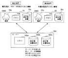
図2は本発明の実施の形態1による半導体開発情報統合装置の模式的な構成を示す。図2(a) において、1は設計部門で作成された情報を保管しているデータベース、2は製造部門で作成された情報を保管しているデータベース、3は評価部門で作成された情報を保管しているデータベースである。また、1aはデータベース1に対してのみならずデータベース2,3に対してもアクセスを行い、設計情報の他に製造情報,評価情報を取得する情報取得手段であり、その取得した情報を設計部門に引き渡し、設計部門はこの情報によって目的とする半導体装置の,自動化された設計を行うものである。2aはデータベース2に対してのみならずデータベース1,3に対してもアクセスを行い、製造情報の他に設計情報,評価情報を取得する情報取得手段であり、その取得した情報を製造部門に引き渡し、製造部門はこの情報によって目的とする半導体装置の,自動化された製造を行うものである。3aはデータベース3に対してのみならずデータベース1,2に対してもアクセスを行い、評価情報の他に設計情報,製造情報を取得する情報取得手段であり、その取得した情報を製造部門に引き渡し、製造部門はこの情報によってその自動化された製造処理を行うものである。これらの情報取得手段はデータベース1,2,3をアクセスするソフトウエア等により実現されている。
【0025】
また、図2(b) において、10は設計部門のEWS(Engineering Workstation )であり、グラフィック端末10a,メモリ10b,副記憶装置10cを有している。100は設計部門のサーバであり、メモリ100aと副記憶装置100bを有している。また、20は製造部門のEWSであり、グラフィック端末20a,メモリ20b,副記憶装置20cを有している。200は設計部門のサーバーであり、メモリ200aと副記憶装置200bを有している。
【0026】
本発明の実施の形態1による半導体開発情報統合装置は以上のように構成されており、半導体装置の開発を行うにあたって、設計部門で作成された設計情報をサーバー100上に実現されたデータベース1に保管し、必要に応じて半導体設計において必要な、アライメント作成、フォトマスクの正・反、容量値、抵抗値、電流値等の情報を、EWS10により検索して得られるリスト(書類や端末画面)を見ながら作成,設定,検索して設計部門で使用するものである。
【0027】
また、製造部門で作成された製造情報をサーバー200上に実現されたデータベース2に保管し、必要に応じて半導体製造において必要な、使用する装置、マスク名、装置に設定する座標情報、処理時間、ロット名等の情報をEWS20により検索して得られるリスト(書類や端末画面)を見ながら作成,設定,検索して製造部門で使用するものである。
【0028】
さらに、評価部門で作成された製造情報を図示しないサーバー上に実現されたデータベース3に保管し、必要に応じて半導体評価において必要な、チップの名称、パッド、TEGの座標値、製造におけるモニタTEGの測定結果、設計仕様等の情報を図示しないEWSにより検索して得られるリスト(書類や端末画面)を見ながら作成,設定,検索して評価部門で使用するものである。
【0029】
このような、データベースの統合化はサーバー間で互いに許可を与えた項目のみにアクセスを行い互いに情報の取得を行うように連携することにより可能になっている。
【0030】
なお、この半導体開発情報統合装置は設計部門と製造部門で別個にサーバーを用意するようにしたが、図15に示すようにこれらを統合するようにしても良い。
【0031】
図において、300は設計部門と製造部門との間で共有化されたサーバーであり、メモリ300aと副記憶装置300b,300cを有している。
【0032】
このサーバー300においては、データの保管場所を切り分けることにより、そのアクセスを限定する。これにより、サーバー300を設計部門と製造部門とで統合化することができる。
【0033】
図1は本実施の形態1による半導体開発情報統合装置の構成例を示し、図において、101は半導体設計にて作成するフォトマスク仕様の電子データと半導体製造工程にて作成する各製造工程の電子データとを同一のデータベースまたは複数のデータベースに統合した統合半導体情報として保管,管理する半導体情報管理装置であり、図2(b) のサーバー100,200もしくは図15のサーバー300により実現されている。102は該半導体情報管理装置101に対し要求を発して、上記統合半導体情報を呼び出して表示を行い、該表示に基づいて設計用データの作成,編集を行う半導体設計用電子端末であり、図2(b) もしくは図15のEWS10により実現されている。103は半導体情報管理装置101に対し要求を発することにより、情報が与えられる半導体設計部門のCAD装置であり、図2(b) もしくは図15のEWS10により実現されている。104は上記半導体情報管理装置101に対し要求を発して、上記統合半導体情報を呼び出し、当該電子端末上に表示を行い、該表示に基づいて製造用データの作成,編集を行う半導体製造用電子端末であり、図2(b) もしくは図15のEWS20により実現されている。105は上記半導体製造用電子端末104により作成,編集された製造用データが与えられ、半導体装置の製造を行う半導体製造装置である。
【0034】
次に動作について説明する。半導体情報管理装置101は半導体設計にて作成するフォトマスク仕様の電子データと半導体製造工程にて作成する各製造工程の電子データとを同一のデータベースまたは複数のデータベースに統合した統合半導体情報として保管,管理しており、半導体設計用電子端末102は該半導体情報管理装置101に対し要求を発して、上記統合半導体情報を呼び出して表示を行い、この表示に基づいて設計用データの作成,編集を行う。CAD装置103は半導体情報管理装置101に対し要求を発することにより、情報が与えられ、半導体製造用電子端末104は上記半導体情報管理装置101に対し要求を発して、上記統合半導体情報を呼び出し、当該電子端末上に表示を行い、該表示に基づいて製造用データの作成,編集を行う。また、半導体製造装置105は上記半導体製造用電子端末104により作成,編集された製造用データが与えられ、半導体装置の製造を自動的に行うものである。
【0035】
すでに述べたように、半導体設計部門は、製品の性能を満足して設計された、一部の直描方式のプロセスを除けばフォトマスクを製造部門に供給することを目的としている。近年、殆んどの半導体製造には十数枚から二十枚を越えるマスク枚数が一般的である。また、半導体製造においては、この供給されたマスクから、一枚あたり二十工程を越える処理を行い製品を完成させている。本実施の形態1は、フォトマスクを介して分業される設計と製造の情報の統合化を、データベースへのアクセス方法を統合することによりその実現を図ったものである。
【0036】
即ち、データベースの統合の方法は、半導体設計部門、半導体製造部門、半導体評価部門において、情報のアドレス名称と連携する電子データ保管可能場所に保管を行い、パソコン、EWS等で個々に情報の入力編集を行う。これらのデータベースをパソコン、EWS等でネットワーク上から検索を行い情報の相互引用を行う。
【0037】
これをより詳しく述べれば、半導体設計において作成されるマスクの名称を記した電子データ、または半導体プロセスで用いられる大工程名を、統一したデータベース、もしくは複数に分散保管させたデータベースとのアクセスを行う上でのアドレスとして検索を行い、一つに統合化されたデータベースとして見えるようにインターフェース上みせかけを行う。または、検索のために、機種毎に決められたマスク名称、半導体製造における機種名、ロット名称を検索の基準として設定し、これに続く各フォトマスク、大工程名に展開をして利用する。
【0038】
上記のデータベースから半導体製造部門が要求するフォトマスクの正・反の情報、精度、半導体製造写真製版に使用する装置が必要とするアライメントマークの種類、フォトマスクのアライメントの順序等の情報を入手することにより、自動パターニングを行う等の半導体設計,半導体製造において自動化装置と接続し、その自動設定により省力化を行う。
【0039】
次に半導体設計について説明する。半導体設計のフォトマスクデザインは、性能を満たす半導体開発のためのフォトマスクを製造する、その電子データ作成を目的としている。フォトマスク作成用電子データは複数層(機種毎の全layer)を同時に設計するため、作成するフォトマスクの一覧表を作成しておき、それを参照しながら設計を行うのが一般的である。本実施の形態1は、半導体設計において、フォトマスクの一覧表を電子データとして作成,編集,保管を行い、データベース化を行う。そのデータベースから引用する情報に基づいて、フォトマスク作成用電子データの自動作成、検証ルールの自動作成を行う。
【0040】
本実施の形態1において使用するデータベースに登録されているデータの項目は、以下のようなものである。
【0041】
即ち、
設計の情報としてのマスク名
設計の情報としてのマスクのノーマル,リバース
設計の情報としてのマスクのサイズ
設計の情報としてのマスクの描画速度
設計の情報としてのマスク内の最小パターン幅
設計の情報としてのマスクを作成するCADデータのlayer
設計の情報としてのマスクのガラス材料、遮光膜材質名またはそれに相当する品名
設計の情報としてのマスクの副番
設計の情報としてのマスクのミラーイメージ
設計の情報としてのマスクの合わせの情報
設計の情報としてのマスクの各ショット,セルサイズ
設計の情報としてのマスクの設計者名
設計の情報としてのマスクの作成開始日と作成完了日
設計の情報としてのマスクのJOBDEC(手順仕様書)
プロセスの情報としての工程一覧
プロセスの情報としての使用マスク名
プロセスの情報としてのシート抵抗値
プロセスの情報としてのコンデンサ容量値
プロセスの情報としてのトランジスタ,FET等の電流値
プロセスの情報としての工程進捗状況
プロセスの情報としての基板材料
プロセスの情報としての基板厚み,誘電率
プロセスの情報としてのメタル抵抗の値
プロセスの情報としての能動層抵抗の値
プロセスの情報としてのコンタクト抵抗の値
プロセスの情報としてのトランジスタの電流値
プロセスの情報としてのトランジスタのしきい値
プロセスの情報としての相互コンダクタンス
このようなデータをフィールドとして有するデータベースを用いることにより、設計部門と製造部門との間でデータのやりとりのオンライン化が可能となる。
【0042】
図3はこの半導体開発情報統合装置を用いて行うようにした半導体装置の開発部門における開発工程の一例を示しており、まずステップS1において、抵抗、コンデンサ、FET、基板等の設計に必要な情報をオンラインで製造部門から入手する。次に、ステップS2において、ステップS1において得られた製造情報を用いて電気設計を行い、ステップS3において、マスクデータ設計を行う。次いで、ステップS4において、マスク製作を行い、ステップS5において、チップサイズ、マスク名、マスク入着日、特定データの面積、目的性能の情報を設計部門から入手し、ステップS6において、ステップS5において得られた設計情報を用いてマスク製造を行う。
【0043】
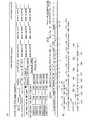
半導体設計において作成するフォトマスク仕様をデータベースから電子端末に呼び出した例を図4(a) に示す。図4(a) において、aで示された記号M−はこのマスクがミラープロジェクション装置にかかるマスクであることを示す。bで示された記号MM01Aはこのマスクの名称を示す。cで示された記号−P4はこのマスクが使用されるプロセス名を示す。dで示された記号39はCADレイヤ名を示す。eで示された記号−Aは副番を示す。fで示された記号Pはポジレジストによるプロセスであることを示す。gで示された記号Rはマスクが反転であることを示す。hで示された記号5はマスクのサイズを示す。iで示された記号0.5 はアドレスユニットでこれが0.5 μmの細かさであることを示す。jで示された記号NOはミラーイメージではないことを示している。kで示された記号3±0.2 は検査パターンの幅が3±0.2 μmであることを示している。lで示された記号…は親のマークのレイヤであることを示している。mで示された記号COREは描画機の名称を示している。nで示された記号は発注副番がAに該当することを示している。
【0044】
なお、この図4(a) では、1層分のみを示したが、実際には複数層存在する。この図4(a) のデータベースに保存された状態のアスキーデータの一例を図4(b) に示す。図4(b) において、X1で示された記号Ga1はマスク設計者の所属グループ名を示す。X2で示された記号mmatuuraはマスク設計者の氏名の略称を示す。X3で示された記号465はマスク設計者の内線番号を示す。X4で示された記号96.02.27はマスク設計日付けを示す。X5で示された記号mm01aaaはセルの名称を示す。X6で示された記号7980はチップサイズにおける一辺の長さを示す。X7で示された記号8000はチップサイズにおける他の辺の長さを示す。X8で示された記号mm01ataはセルの名称を示す。X9で示された記号7980はチップサイズにおける一辺の長さを示す。X10で示された記号8000はチップサイズにおける他の辺の長さを示す。X11で示された記号mm01amaはセルの名称を示す。X12で示された記号7980はチップサイズにおける一辺の長さを示す。X13で示された記号8000はチップサイズにおける他の辺の長さを示す。X14で示された記号mm01asaはセルの名称を示す。X15で示された記号7980はチップサイズにおける一辺の長さを示す。X16で示された記号8000はチップサイズにおける他の辺の長さを示す。X17で示された記号96.02.21は日付を示す。
【0045】
X18で示された記号MIRはこのマスクがマスタであることを示す。X19で示された記号M−はこのマスクがミラープロジェクション装置にかかるマスクであることを示す。X20で示された記号MM01Aはこのマスクの名称を示す。X21で示された記号P4はこのマスクが使用されるプロセス名を示す。X21で示された記号39はCADレイヤ名を示す。X22で示された記号Aは副番を示す。X23で示された記号Pはポジレジストプロセスであることを示す。X24で示された記号Rはマスクが反転であることを示す。X25で示された記号5はマスクのサイズを示す。X26で示された記号0.5 はアドレスユニットでこれが0.5 μmの細かさであることを示す。X27で示された記号NOはミラーイメージではないことを示している。X28,X29で示された記号3.00,0.2 は検査パターンの幅が3±0.2 μmであることを示している。X30で示された記号G1は親のマークのレイヤであることを示している。X31で示された記号COREは描画機の名称を示している。X32で示された記号nilはこの項目に該当する記号が無である旨を示している。
【0046】
この図4(b) のX19からX31は図4(a) のaからmまでに対応しているものである。
【0047】
このように、設計部門で登録するデータである図4(a) の表を図4(b) のようにアスキーデータで保存することにより、コンピュータ間で互換性を有し、しかもコンピュータ間で通信を行う際の文字化けが生じない。
【0048】
半導体製造に使用する写真製版用の露光装置は各露光装置メーカーが取り決めたアライメント形状をフォトマスク上で作成する必要がある。図4(a) (実際には複数層存在する)で示したフォーマットからアライメント群を自動作成した例を図5に示す。
【0049】
図5において、A1,A2はマスタ用のアライメントマークであり、露光装置固有のものである。A3〜A5は露光装置のメーカがカタログにて推奨しているマスタ用のアライメントマークである。R1〜R9はレティクル用のマークであり、Pはウエハ上のレジストの現像の解像度を検査するための現像検査パターンである。
【0050】
半導体製造に使用する写真製版用の露光装置に設定を行うための座標値をCAD上で抽出を行った例を図6に示す。
【0051】
この図6は1枚のウエハの上に複数のチップのパターンMM01AM,MM01AT,MM01AA,MM01ABを形成する例を示している。
【0052】
半導体製造において説明する。半導体製造における工程表の一例を図7に示す。この図7は或る一工程のみを示している。マスク名、アライメントマーク座標等は設計が使用したフォトマスクの一覧表をデータベースから引用する。図7中のAがこれに該当し、図4(a) の項目a〜fがここに引用される。なお、Bは製造の際の溶剤やその処理時間等を示している。
【0053】
このように、半導体製造において、仕様マスク搬出等の設定は電子データ化された工程表からなされる。
【0054】
半導体評価においても、半導体設計,半導体製造と同様にデータベースの相互利用を行う。
【0055】
データベースの構築方法は次のようになる。データの保存はパソコン、EWS等における副記憶装置で改訂や更新等の管理が行える、有線もしくは無線で接続された監視可能な記憶装置とする。データベースを共有するため、数値、文字情報はバイナリーデータ、もしくはアスキーデータで記述するようにしており、これにより、同一、もしくは異機種間のコンピュータ同士が同一の数値や文字情報を復元することができる。また、データベース管理システムはデータベースの改訂、更新に対するセキュリティ機能をサポートしているものを使用する。
【0056】
このように、本実施の形態1によれば、半導体情報管理装置により半導体設計にて作成するフォトマスク仕様の電子データと、半導体製造工程にて作成する各製造工程の電子データとを、同一のデータベースまたは複数のデータベースに統合した統合半導体情報として保管,管理し、半導体設計用電子端末により該半導体情報管理装置に対し要求を発して、上記統合半導体情報を呼び出して表示を行い、この表示に基づいて設計用データの作成,編集を行うとともに、CAD装置より半導体情報管理装置に対し統合情報呼び出し要求を発することにより、統合化された半導体情報が与えられ、半導体製造用電子端末より上記半導体情報管理装置に対し統合情報呼び出し要求を発して、上記統合半導体情報を呼び出し、当該電子端末上に表示を行い、該表示に基づいて製造用データの作成,編集を行い、さらに半導体製造装置により上記半導体製造用電子端末により作成,編集された製造用データが与えられ、半導体装置の製造を自動的に行うようにしたので、自動化装置に対する人手による条件設定が不要になり、半導体設計部門、半導体製造部門、半導体評価部門の省力化が図れる効果がある。
【0057】
実施の形態2.
なお、上記実施の形態1では、特に半導体設計部門におけるEWS(CAD装置)については特に詳しく触れなかったが、これは、図8に示すごとく、半導体設計において、共有化されたデータベースから半導体製造部門が要求するフォトマスクの正・反の情報、精度、半導体製造写真製版に使用する装置が必要とするアライメントマークの種類、フォトマスクのアライメントの順序、等の情報を入手することにより自動的にパターニングを行うものとすることができる。
【0058】
図8において、S10はデータベースから情報を取得するステップ、S11はステップS10で取得した情報のなかからマスクの正・反情報を取得するステップ、S12はCAD装置上で遮光帯を自動作成するか否かを判定するステップ、S13はステップS10で取得した情報のなかから精度情報を取得するステップ、S14はこの精度情報に基づいてマスク描画部門への指示および検査パターンの作成を行うステップ、S16はステップS10で取得した情報のなかから製造に使用する写真製版装置名を取得するステップ、S17はこの写真製版装置名に基づいてアライメントマークの種類を判断するステップ、S18はステップS10で取得した情報のなかからチップサイズ及びウエハ上での配置情報を取得するステップ、S19はこのチップサイズ及びウエハ上での配置情報に基づいてアライメントマーク形成位置を計算するステップ、S20はステップS10で取得した情報のなかからマスクの使用順序を取得するステップ、S21はこのマスクの使用順序に基づいてアライメントマークの形成順序の判断を行うステップ、S22はステップS17で判断されたアライメントマークの種類,ステップS19で計算されたアライメントマークの形成位置およびステップS21で判断されたアライメントマークの形成順位に基づいてアライメントマークの自動作成を行うステップである。
【0059】
次に動作について説明する。CAD装置は図2に示すように、グラフィック端末10a,メモリ10b,副記憶装置10cの他に図示しないCPUを内蔵しており、このCPUが以下の処理を行うことにより、自動的にパターニングを行うものである。
【0060】
即ち、ステップS10において、半導体製造部門と半導体設計部門で共有化されたデータベースより各種の情報の取得を行い、ステップS11において、そのなかからマスクが正か反かの情報を取得する。ステップS12において、これが正か反かを判断し、反であれば遮光帯の自動作成を行い、正であれば遮光帯の作成は行なわない。
【0061】
また、ステップS13において、ステップS10にて得られた各種の情報のなかから精度情報を取得し、ステップS14において、この精度情報を用いてマスク描画部門への指示を行うとともに、検査パターンの作成を行う。
【0062】
また、ステップS16において、ステップS10にて得られた各種の情報のなかから製造に使用する写真製版装置名を得て、ステップS17において、形成すべきアライメントマークの種類を判断する。
【0063】
さらに、ステップS18において、ステップS10にて得られた各種の情報のなかからチップサイズおよびウエハ上での配置情報を取得し、ステップS19において、これに基づきアライメントマークの形成されるべき位置を計算する。
【0064】
そして、ステップS20において、ステップS10にて得られた各種の情報のなかからマスクの使用順序を取得し、ステップS21においてこれに基づきアライメントマークの形成されるべき順位を判断する。
【0065】
そして、ステップS22において、ステップS17において判断されたアライメントマークの種類,ステップS19において計算されたアライメントマークの形成位置、およびステップS21において判断されたアライメントマークの形成順位を参照し、これらの情報に基づいてアライメントマークを自動的に作成する。
【0066】
このように、本実施の形態2によれば、データベースが半導体設計部門と半導体製造部門で共有化されていることを利用し、このデータベースを参照することにより、CAD装置の側で自動的にアライメントマーク等のパターンを発生することができ、半導体設計の省力化の面でより有利な装置を得ることができる。
【0067】
実施の形態3.
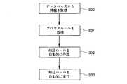
また、上記CAD装置は、半導体設計において、検証ルールを自動的に作成し、その実行を行うものとしてもよい。
【0068】
図9において、S30はデータベースから情報を取得するステップ、S31はステップS30で取得した情報のなかからプロセスルールを取得するステップ、S32はこのプロセスルールに基づいて検証ルールを自動的に作成するステップ、S33はこの作成された検証ルールを自動的に実行するステップである。
【0069】
次に動作について説明する。CAD装置に内蔵されたCPUは、ステップS30において、半導体設計部門と半導体製造部門で共有化されたデータベースより各種の情報の取得を行い、ステップS31において、そのなかから半導体製造部門が要求する配線幅、配線間隙等のプロセスルールを取得する。そして、ステップS32において、これらのプロセスルールに基づいて検証ルールを自動的に作成し、ステップS33において、この自動作成された検証ルールを自動的に実行する。
【0070】
このように、本実施の形態3によれば、データベースが半導体設計部門と半導体製造部門で共有化されていることを利用し、このデータベースを参照することにより、CAD装置の側で自動的に検証ルールを作成し、かつこれを自動実行するようにしたので、半導体設計の省力化の面でより有利な装置を得ることができる。
【0071】
実施の形態4.
また、半導体装置の製造を行う自動化された半導体製造装置については、これに図10に示すごとく、マスクをいつ作成し、いつでき上がってくるかを判明させる機能をもたせてもよい。
【0072】
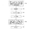
図10において、S40はデータベースから情報を取得するステップ、S41はステップS40で取得した情報のなかから作成マスクの入着予定日時の取得を行うステップ、S42はステップS40で取得した情報に基づき使用マスクの自動取り出し搬送装置の制御を行うステップ、S43はステップS40で取得した情報に基づき描画装置の指定を行うステップ、S44はステップS40で取得した情報に基づき処理時間の管理を行うステップ、S45はステップS40で取得した情報に基づき工程管理を行うステップ、S46はステップS40で取得した情報に基づき進捗管理を行うステップ、S47は特定マスクの指定した範囲に存在する図形面積の取得による装置への数値設定を行うステップ、S48はステップS40で取得した情報に基づき検査パターンの座標指定をCADデータと写真製版後のウエハ上の座標とを複合的に計算して割り出すステップである。
【0073】
次に動作について説明する。半導体製造装置はその自動化された製造処理のためにCPUを内蔵しており、この内蔵されたCPUは、ステップS40において、半導体設計部門と半導体製造部門で共有化されたデータベースより各種の情報の取得を行い、ステップS41において、ステップS40にて取得したデータのなかからその作成マスクの入着予定日時の取得を行う。また、ステップS42において、ステップS40にて取得したデータに基づいてマスクの自動取り出し搬送装置の制御を行うことにより、使用すべきマスクの取り出しと搬送を行う。また、ステップS43において、ステップS40にて取得したデータによってプロセスの種類および使用マスク名が判明するため、写真製版の描画装置の指定を行う。また、ステップS44において、ステップS40にて取得したデータに基づきプロセスの処理時間の管理を行う。また、ステップS45,S46において、ステップS40にて取得したデータに基づき工程管理,進捗管理を行う。また、ステップS47において、ステップS40にて取得したデータに基づき特定のマスクの指定した範囲に存在する図形面積を取得することによる製造装置への数値設定を行う。さらに、ステップS48において、ステップS40にて取得したデータに基づき検査パターンの座標指示をCADデータと写真製版後のウエハ上の座標とを複合的に計算して割り出すことにより、検査パターンがどこに存在するかを判定する。
【0074】
このように、本実施の形態4によれば、データベースが半導体設計部門と半導体製造部門で共有化されていることを利用し、このデータベースを参照することにより、半導体製造装置の側で自動的に作成マスクの入着予定日時の取得、使用マスクの自動取り出し搬送装置の制御、描画装置の指定、処理時間の管理、工程管理、進捗管理、特定マスクの指定した範囲に存在する図形面積の取得による装置への数値設定、検査パターンの座標指示を、CADデータと写真製版後のウエハ上の座標とを複合的に計算して割り出す処理を行うようにしたので、マスクをいつ作成し、そのマスクがいつできあがってくるかが自動的に判明するため、半導体製造の省力化の面でより有利な装置を得ることができる。
【0075】
実施の形態5.
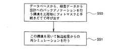
また、上記CAD装置は、半導体設計において、製造結果からの再シミュレーションを行うようにしてもよい。
【0076】
図11において、S50はデータベースから検査データから設計へのバックアノテーションを行う環境を工程毎にフォトマスクと系統だてて呼び出すステップ、S51はこの環境を用いて製造結果からの再シミュレーションを行うステップである。
【0077】
次に動作について説明する。CAD装置はCPUを内蔵しており、この内蔵されたCPUは、ステップS50において、製造工程を終えた、あるいは製造工程中の検査データから設計へのバックアノテーションを行う環境を、データベースより工程ごとにフォトマスクと系統だてて呼び出す。そして、この呼び出した環境に基づいて、ステップS51において、製造結果からの再シミュレーションを行う。
【0078】
このように、本実施の形態5によれば、データベースが半導体設計部門と半導体製造部門で共有化されていることを利用し、CAD装置において、製造工程を終えた、あるいは製造工程中の検査データを取得し、これを用いて製造結果からの再シミュレーションを容易に行うことができる。このため、例えば10μm角の正方形で200Ωのシート抵抗において、片方の辺が延びて、抵抗値が250Ωになったり180Ωになったりしてばらつくことがあるが、これを設計値に戻すことにより、正確な抵抗値を実現することができる。さらにこれは、コンデンサの容量値やFETの電流値の制御にも用いることができる。
【0079】
実施の形態6.
また、半導体開発情報統合装置のデータベースは、これに半導体装置の機種別、工程別に雛形となるデータを登録するとともに、設計部門と製造部門で重複して発生した情報を一本化して登録するようにしてもよい。
【0080】
図12において、S60は本半導体開発情報統合装置のデータベースに半導体装置の機種別、工程別に雛形となるデータを登録する工程、S61はこのデータベースに設計部門と製造部門で重複して発生した情報を一本化して登録する工程である。
【0081】
次に動作について説明する。半導体開発情報統合装置のサーバーにはCPUが内蔵されており、このCPUはその副記憶装置上に実現されるデータベースに対し、ステップS60において、半導体装置の機種別、工程別に雛形となるデータを登録し、ステップS61において、このデータベースに設計部門と製造部門で重複して発生した情報を一本化して登録する。
【0082】
このように、本実施の形態6によれば、半導体開発情報統合装置のデータベースに、半導体装置の機種別、工程別に雛形となるデータを登録するとともに、設計部門と製造部門で重複して発生した情報を一本化して登録するようにしたので、これにより、これらの情報作成作業の効率化を図ることができる。そして、プロセスが1つの製造ラインで規格化されているので、製造ラインで例えば10種類の処理が存在すれば、10種類の処理を登録しておき、これを適宜選択することにより、工程管理を容易に行うこともできる。
【0083】
実施の形態7.
また、上記CAD装置は、半導体装置の厚み情報を取り込むことにより、三次元CADのZ軸の指定や、デバイスシミュレーション情報を獲得することが可能である。
【0084】
図13において、S70はデータベースより半導体装置の厚み情報を取り込むステップ、S71は三次元CADのZ軸の指定やデバイスシミュレーションの情報の植え込み(獲得)を行うステップである。
【0085】
次に動作について説明する。CAD装置はCPUを内蔵しており、この内蔵されたCPUは、ステップS70において、データベースより半導体装置の厚み情報を取り込み、ステップS71において、この取り込まれた情報を用いて三次元CADのZ軸の指定やデバイスシミュレーションの情報の獲得を行う。
【0086】
このように、本実施の形態7によれば、データベースが半導体設計部門と半導体製造部門で共有化されていることを利用し、CAD装置においてデータベースより半導体装置の厚み情報を取り込むことにより、三次元CADのZ軸の指定や、デバイスシミュレーション情報を植え込むことが可能である。このため、単なる2次元的な配線の幅のみならずそのZ軸方向の厚みも判明するため、3次元での電気的特性が判明する。
【0087】
実施の形態8.
さらに、半導体装置の評価に用いる半導体評価装置は、上記CAD装置のCAD情報を取り込むことにより、オンウエハ評価時における座標値の指定を行うようにしてもよい。
【0088】
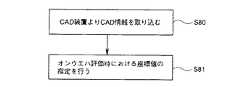
図14において、S80はCAD装置よりCAD情報を取り込むステップ、S81はオンウエハ評価時における座標値の指定を行うステップである。
【0089】
次に動作について説明する。半導体評価装置はCPUを内蔵しており、この内蔵されたCPUは、ステップS80において、CAD装置よりCAD情報を取り込み、ステップS81において、このステップS80にて取得したCAD情報に基づいてオンウエハ評価時における座標値の指定を行う。
【0090】
このように、本実施の形態8によれば、データベースが半導体設計部門と半導体製造部門で共有化されていることを利用し、半導体評価装置において、CAD装置よりCAD情報を取り込み、このCAD情報に基づいてオンウエハ評価時における座標値の指定を行うことができる。このため、オンウエハ評価を行う際にウエハを搭載したステージを動かすよりもより正確にウエハを移動させることができ、オンウエハ評価をより正確に行うことができる。
【0091】
【発明の効果】
以上のように、本願の請求項1の発明に係る半導体開発情報統合装置によれば、半導体装置の設計部門にて作成するフォトマスク仕様を電子データ化してなる一覧表と半導体装置の製造部門にて作成する各製造工程を電子データ化してなる指示書と半導体製造工程での中間評価結果を電子データ化してなる一覧表とを同一のデータベースまたは複数のデータベースに統合して保管,管理する半導体情報管理装置と、該半導体情報管理装置に対し統合情報呼び出し要求を発して、当該電子端末上にシートメニュー,フォームメニューとして各工程別に列もしくはページを分けて表示を行い、この画面上で半導体設計部門,半導体製造部門の人員がデータの作成、編集を行う電子端末と、上記半導体情報管理装置に対し統合情報呼び出し要求を発したとき、上記半導体情報管理装置により上記統合された半導体情報が与えられ、半導体設計において、上記のデータベースから半導体製造部門が要求するフォトマスクの正・反の情報、精度、半導体製造写真製版に使用する装置が必要とするアライメントマークの種類、およびフォトマスクのアライメントの順序の情報を入手することにより自動的にパターニングを行う、半導体設計部門のCAD装置と、上記半導体情報管理装置に対し統合情報呼び出し要求を発したとき、上記半導体情報管理装置により上記統合された半導体情報が与えられる半導体製造装置とを備えるようにしたので、自動化装置に対する人手による条件設定が不要になり、半導体設計部門、半導体製造部門、半導体評価部門の省力化が図れるとともに、パターニングを自動的に行うことができ、この面からも省力化を図ることができる効果がある。
【0092】
また、本願の請求項2の発明に係る半導体開発情報統合装置によれば、半導体装置の設計部門にて作成するフォトマスク仕様を電子データ化してなる一覧表と半導体装置の製造部門にて作成する各製造工程を電子データ化してなる指示書と半導体製造工程での中間評価結果を電子データ化してなる一覧表とを同一のデータベースまたは複数のデータベースに統合して保管,管理する半導体情報管理装置と、該半導体情報管理装置に対し統合情報呼び出し要求を発して、当該電子端末上にシートメニュー,フォームメニューとして各工程別に列もしくはページを分けて表示を行い、この画面上で半導体設計部門,半導体製造部門の人員がデータの作成、編集を行う電子端末と、上記半導体情報管理装置に対し統合情報呼び出し要求を発したとき、上記半導体情報管理装置により上記統合された半導体情報が与えられ、半導体装置の厚み情報を取り込むことにより、三次元CADのZ軸の指定、デバイスシミュレーション情報の獲得が可能な、半導体設計部門のCAD装置と、上記半導体情報管理装置に対し統合情報呼び出し要求を発したとき、上記半導体情報管理装置により上記統合された半導体情報が与えられる半導体製造装置とを備えるようにしたので、自動化装置に対する人手による条件設定が不要になり、半導体設計部門、半導体製造部門、半導体評価部門の省力化が図れるとともに、三次元CADのZ軸の指定、デバイスシミュレーション情報の獲得が可能となり、この面からも省力化を図ることができる効果がある。
【0093】
また、本願の請求項3の発明に係る半導体開発情報統合装置によれば、請求項1または2の半導体開発情報統合装置において、上記半導体製造装置は、半導体装置の製造において、上記のデータベースから情報取り込みを行うことにより、作成マスクの入着予定日時の取得、使用マスクの自動取り出し搬送装置の制御、描画装置の指定、処理時間の管理、工程管理、進捗管理、特定マスクの指定した範囲に存在する図形面積の取得による装置への数値設定、および検査パターンの座標指示を、CADデータと写真製版後のウエハ上の座標とを複合的に計算して割り出す処理を行うものとしたので、自動化装置に対する人手による条件設定が不要になり、半導体設計部門、半導体製造部門、半導体評価部門の省力化が図れるとともに、作成マスクの入着予定日時の取得、使用マスクの自動取り出し搬送装置の制御、描画装置の指定、処理時間の管理、工程管理、進捗管理、特定マスクの指定した範囲に存在する図形面積の取得による装置への数値設定、検査パターンの座標指示を、CADデータと写真製版後のウエハ上の座標とを複合的に計算して割り出す処理を行うことができ、この面からも省力化を図ることができる効果がある。
【0094】
また、本願の請求項4の発明に係る半導体開発情報統合装置によれば、請求項1または2の半導体開発情報統合装置において、上記半導体開発情報統合装置は、そのデータベースに半導体装置の機種別、工程別に雛形となるデータを登録するとともに、設計部門と製造部門で重複して発生した情報を一本化して登録するようにしたので、自動化装置に対する人手による条件設定が不要になり、半導体設計部門、半導体製造部門、半導体評価部門の省力化が図れるとともに、設計部門と製造部門で重複して発生した情報を一本化して登録することができ、この面からも省力化を図ることができる効果がある。
【0095】
また、本願の請求項5の発明に係る半導体開発情報統合装置によれば、請求項1または2の半導体開発情報統合装置において、上記半導体装置の評価に用いる半導体評価装置は、上記CAD装置のCAD情報を取り込むことにより、オンウエハ評価時における座標値の指定を行うようにしたので、自動化装置に対する人手による条件設定が不要になり、半導体設計部門、半導体製造部門、半導体評価部門の省力化が図れるとともに、オンウエハ評価時における座標値の指定を行うことができ、この面からも省力化を図ることができる効果がある。
【図面の簡単な説明】
【図1】本発明の実施の形態1による半導体開発情報統合装置の構成例を示す図である。
【図2】本発明の実施の形態1による半導体開発情報統合装置の模式的な構成例を示す図である。
【図3】本発明の実施の形態1による半導体開発情報統合装置を用いて行うようにした半導体装置の開発部門における開発工程の一例を示す図である。
【図4】半導体設計において作成するフォトマスク仕様をデータベースから電子端末に呼び出した例を示す図である。
【図5】図4で示したフォーマットからアライメント群を自動作成した例を示す図である。
【図6】半導体製造に使用する写真製版用の露光装置に設定を行うための座標値をCAD上で抽出を行った例を示す図である。
【図7】半導体製造における工程表の一例を示す図である。
【図8】本発明の実施の形態2におけるCAD装置が行う処理を示すフローチャート図である。
【図9】本発明の実施の形態3におけるCAD装置が行う処理を示すフローチャート図である。
【図10】本発明の実施の形態4における半導体製造装置が行う処理を示すフローチャート図である。
【図11】本発明の実施の形態5におけるCAD装置が行う処理を示すフローチャート図である。
【図12】本発明の実施の形態6における半導体開発情報統合装置が行う処理を示すフローチャート図である。
【図13】本発明の実施の形態7におけるCAD装置が行う処理を示すフローチャート図である。
【図14】本発明の実施の形態8における半導体評価装置が行う処理を示すフローチャート図である。
【図15】本発明の実施の形態1による半導体開発情報統合装置の他の模式的な構成例を示す図である。
【図16】従来の半導体開発における設計部門と製造部門,評価部門の情報の交換の様式を示す図である。
【図17】従来の半導体装置の開発部門における開発工程の一例を示す図である。
【符号の説明】
101 半導体情報管理装置、102 半導体設計用電子端末、103 CAD装置、104 半導体製造用電子端末、105 半導体製造装置、1,2,3データベース、1a,2a,3a データベースへのアクセスを行い、情報を取得する手段、10,20 EWS、10a,20a グラフィック端末、 10b,20a,20b メモリ、10c,20c 副記憶装置、100, 200,300 サーバー、100a,200a,300a メモリ、100b,200b,300b,300c 副記憶装置。[0001]
BACKGROUND OF THE INVENTION
The present invention relates to a semiconductor development information integration device, and more particularly, to create and edit conditions for an automatic device for semiconductor design and manufacture (including evaluation), and more specifically, design and manufacture thereof. The present invention relates to an apparatus that eliminates manual information exchange by integrating information database for designing and manufacturing for setting conditions in an automated apparatus for manufacturing.
[0002]
[Prior art]
Semiconductor design and semiconductor manufacturing are separated from each other by the delivery of photomasks, and automation is also progressing individually for both. This is because automation equipment vendors specialize in semiconductor design equipment and semiconductor manufacturing equipment, and it is common for vendors to differ between semiconductor design and semiconductor manufacturing. There are many differences, and even vendors dealing with both semiconductor design and semiconductor manufacturing are not well-versed in automating both, so it is difficult to share and use information Because.
[0003]
In recent years, in the semiconductor manufacturing department, the paperless process management table in the clean room is being completed, but the integration of electronic data for exchanging information with the design department has been delayed.
[0004]
Next, a method of exchanging information between each department in conventional semiconductor development will be described. FIG. 16 is a diagram showing a format of information exchange between a design department, a manufacturing department, and an evaluation department in conventional semiconductor development. In FIG. 16 (a), 1b is a database that stores information created in the design department.
[0005]
In FIG. 16B,
[0006]
Usually, the development department of the semiconductor device possesses the development support apparatus as described above, and when developing the semiconductor device, the design information created by the design department is stored in the
[0007]
Further, manufacturing information created in the manufacturing department is stored in the
[0008]
Further, manufacturing information created by the evaluation department is stored in a
[0009]
However, since the
[0010]
FIG. 17 shows an example of a development process in the conventional semiconductor device development department. First, in step S1a, information necessary for designing resistors, capacitors, FETs, substrates, etc. is obtained from documents or electronic data existing individually. Get manufacturing information. Next, in step S2, electrical design is performed using the manufacturing information obtained in step S1a, and mask data is designed in step S3. Next, in step S4, a mask is manufactured, and in step S5a, the chip size, mask name, mask arrival date, specific data area, target performance, and the design information are obtained from documents or electronic data existing individually. In step S6, a mask is manufactured using the design information obtained in step S5a.
[0011]
[Problems to be solved by the invention]
Information exchange in the conventional semiconductor design department is performed as described above, and in a more specific example, in the design stage in semiconductor development, electrical design is performed with a simulator, but when setting conditions in the simulator, Requires information from manufacturing and evaluation departments. However, the information from the manufacturing department and the evaluation department is not integrated with the information from the design department. For this reason, a piece of information is written on paper for each model or converted into a volume etc. After receiving it, it is manually set manually.
[0012]
In this way, in the development of semiconductors, although most of the information held by the design department has been converted to electronic data, there is a problem with the interface. Then, the data was set by manual operation, that is, manual input work.
[0013]
For this reason, there has been a problem that manpower is required for simple information interface work, which is an obstacle to cost reduction in manufacturing a semiconductor device.
[0014]
The present invention has been made in order to solve the above-described problems of the prior art, and integrates a database for storing information on design and manufacturing to achieve epoch-making automation and labor saving of semiconductor device manufacturing. An object of the present invention is to obtain a semiconductor development information integration device capable of performing the above.
[0015]
[Means for Solving the Problems]
According to a first aspect of the present invention, there is provided a semiconductor development information integration device.List of photomask specifications created in the semiconductor device design department converted to electronic data, instructions for each manufacturing process created in the semiconductor device manufacturing department converted to electronic data, and intermediate evaluation results in the semiconductor manufacturing process And a semiconductor information management device that integrates and stores the electronic data into a single database or a plurality of databases, and issues an integrated information call request to the semiconductor information management device. A sheet menu and a form menu are displayed separately in columns or pages for each process, and on this screen, an electronic terminal in which a person in the semiconductor design department and semiconductor manufacturing department creates and edits data, and the semiconductor information management apparatus When the integrated information call request is issued, the integrated semiconductor information is given by the semiconductor information management device. In semiconductor design, the information on photomask positive / reverse information required by the semiconductor manufacturing department from the above database, accuracy, types of alignment marks required by the equipment used for semiconductor manufacturing photoengraving, and photomask alignment order When the integrated information call request is issued to the CAD device of the semiconductor design department that automatically performs patterning by obtaining information and the semiconductor information management device, the integrated semiconductor information is received by the semiconductor information management device. GivenAnd a semiconductor manufacturing apparatus.
[0016]
According to a second aspect of the present invention, there is provided a semiconductor development information integration apparatus comprising: a list formed by converting photomask specifications created in a semiconductor device design department into electronic data; and manufacturing steps created in a semiconductor device manufacturing department. A semiconductor information management device that integrates and stores and manages an instruction form converted into electronic data and a list formed by converting intermediate evaluation results in the semiconductor manufacturing process into the same database or a plurality of databases, and the semiconductor information The integrated information call request is issued to the management device, and the column or page is displayed for each process as a sheet menu and form menu on the electronic terminal. On this screen, the personnel of the semiconductor design department and semiconductor manufacturing department When an integrated information call request is issued to the electronic terminal for creating and editing data and the semiconductor information management device, the semiconductor Semiconductor information the integration provided by multicast management deviceBy importing the thickness information of the semiconductor device, it is possible to specify the Z axis of 3D CAD and acquire device simulation information.A semiconductor design department CAD device and a semiconductor manufacturing device to which the integrated semiconductor information is given by the semiconductor information management device when an integrated information call request is issued to the semiconductor information management device. is there.
[0017]
A semiconductor development information integration device according to
[0018]
A semiconductor development information integration device according to claim 4 of the present invention is3. The semiconductor development information integration device according to
[0019]
A semiconductor development information integration device according to
[0024]
DETAILED DESCRIPTION OF THE INVENTION
Hereinafter, embodiments of the present invention will be described with reference to the drawings.
FIG. 2 shows a schematic configuration of the semiconductor development information integration apparatus according to the first embodiment of the present invention. In FIG. 2 (a), 1 is a database storing information created by the design department, 2 is a database storing information created by the manufacturing department, and 3 is storing information created by the evaluation department. Database. Further, 1a is an information acquisition means for accessing not only the
[0025]
In FIG. 2B,
[0026]
The semiconductor development information integration device according to the first embodiment of the present invention is configured as described above. When developing a semiconductor device, the design information created by the design department is stored in the
[0027]
In addition, manufacturing information created in the manufacturing department is stored in the database 2 realized on the
[0028]
Further, manufacturing information created by the evaluation department is stored in a
[0029]
Such database integration is made possible by linking the servers so as to access only the items permitted to each other and acquire information from each other.
[0030]
In this semiconductor development information integration apparatus, the server is prepared separately in the design department and the manufacturing department, but these may be integrated as shown in FIG.
[0031]
In the figure,
[0032]
In this
[0033]
FIG. 1 shows a configuration example of a semiconductor development information integration apparatus according to the first embodiment. In FIG. 1,
[0034]
Next, the operation will be described. The semiconductor
[0035]
As already mentioned, the semiconductor design department aims to supply photomasks to the manufacturing department except for some direct drawing processes that are designed to satisfy product performance. In recent years, in most semiconductor manufacturing, the number of masks exceeding ten to twenty is common. Further, in semiconductor manufacturing, a product is completed by performing processing exceeding 20 steps per sheet from the supplied mask. In the first embodiment, integration of design and manufacturing information divided through a photomask is realized by integrating a database access method.
[0036]
In other words, the database integration method is that the semiconductor design department, the semiconductor manufacturing department, and the semiconductor evaluation department store data in an electronic data storage location linked to the address name of the information, and input and edit information individually on a personal computer, EWS, etc. I do. These databases are searched on the network with a personal computer, EWS, etc., and information is mutually cited.
[0037]
More specifically, access is made to a database in which electronic data describing the name of a mask created in semiconductor design or a large process name used in a semiconductor process is unified or stored in a distributed manner. The search is performed using the above address, and the interface is displayed so that it can be seen as an integrated database. Alternatively, for search, a mask name determined for each model, a model name in semiconductor manufacturing, and a lot name are set as a reference for search, and are expanded and used for each subsequent photomask and large process name.
[0038]
From the above database, obtain information such as photomask normal / reverse information required by the semiconductor manufacturing department, accuracy, types of alignment marks required by the equipment used for semiconductor photoengraving, photomask alignment order, etc. Thus, it is connected to an automation device in semiconductor design and semiconductor manufacturing such as automatic patterning, and labor saving is achieved by the automatic setting.
[0039]
Next, semiconductor design will be described. The photomask design of semiconductor design aims at producing electronic data for manufacturing a photomask for semiconductor development that satisfies the performance. Since electronic data for photomask creation is designed in multiple layers (all layers for each model) at the same time, it is common to create a list of photomasks to be created and design with reference to the list. In the first embodiment, in semiconductor design, a photomask list is created, edited, and stored as electronic data to create a database. Based on the information cited from the database, electronic data for photomask creation is automatically created and verification rules are automatically created.
[0040]
The items of data registered in the database used in the first embodiment are as follows.
[0041]
That is,
Mask name as design information
Normal or reverse mask as design information
Mask size as design information
Mask drawing speed as design information
Minimum pattern width in the mask as design information
A layer of CAD data that creates a mask as design information
Mask glass material, light shielding film material name or equivalent product name as design information
Sub-number of mask as design information
Mirror image of mask as design information
Mask alignment information as design information
Each shot and cell size of mask as design information
Mask designer name as design information
Creation start date and creation completion date of mask as design information
Mask JOBDEC (procedure specification) as design information
Process list as process information
Use mask name as process information
Sheet resistance value as process information
Capacitor value as process information
Current values of transistors, FETs, etc. as process information
Process progress as process information
Substrate materials as process information
Substrate thickness and dielectric constant as process information
Metal resistance value as process information
Active layer resistance value as process information
Contact resistance value as process information
Transistor current value as process information
Transistor threshold as process information
Mutual conductance as process information
By using a database having such data as fields, data exchange between the design department and the manufacturing department can be made online.
[0042]
FIG. 3 shows an example of the development process in the development department of the semiconductor device performed using this semiconductor development information integration device. First, in step S1, information necessary for designing resistors, capacitors, FETs, substrates, etc. Get online from the manufacturing department. Next, in step S2, electrical design is performed using the manufacturing information obtained in step S1, and mask data is designed in step S3. Next, in step S4, a mask is manufactured. In step S5, information on the chip size, mask name, mask arrival date, specific data area, and target performance is obtained from the design department. In step S6, the information is obtained in step S5. The mask is manufactured using the designed information.
[0043]
FIG. 4A shows an example in which the photomask specification created in the semiconductor design is called from the database to the electronic terminal. In FIG. 4A, the symbol M- indicated by a indicates that this mask is a mask applied to the mirror projection apparatus. Symbol MM01A indicated by b indicates the name of this mask. The symbol -P4 indicated by c indicates the process name in which this mask is used. A
[0044]
In FIG. 4 (a), only one layer is shown, but there are actually a plurality of layers. An example of ASCII data stored in the database shown in FIG. 4 (a) is shown in FIG. 4 (b). In FIG. 4B, symbol Ga1 indicated by X1 indicates the group name of the mask designer. The symbol mmtuura indicated by X2 indicates the abbreviation of the name of the mask designer. A
[0045]
The symbol MIR indicated by X18 indicates that this mask is the master. A symbol M- indicated by X19 indicates that this mask is a mask applied to the mirror projection apparatus. A symbol MM01A indicated by X20 indicates the name of this mask. A symbol P4 indicated by X21 indicates a process name in which this mask is used. A
[0046]
X19 to X31 in FIG. 4B correspond to a to m in FIG. 4A.
[0047]
In this way, the table shown in FIG. 4 (a), which is data registered in the design department, is saved as ASCII data as shown in FIG. 4 (b), so that the computers are compatible and communicate with each other. There is no garbled character when performing.
[0048]
An exposure apparatus for photoengraving used for semiconductor manufacture needs to create an alignment shape determined by each exposure apparatus manufacturer on a photomask. FIG. 5 shows an example in which alignment groups are automatically created from the format shown in FIG. 4 (a) (actually, there are a plurality of layers).
[0049]
In FIG. 5, A1 and A2 are alignment marks for the master, which are unique to the exposure apparatus. A3 to A5 are master alignment marks recommended by the manufacturer of the exposure apparatus in the catalog. R1 to R9 are reticle marks, and P is a development inspection pattern for inspecting the resolution of development of the resist on the wafer.
[0050]
FIG. 6 shows an example in which coordinate values for setting in an exposure apparatus for photoengraving used for semiconductor manufacture are extracted on CAD.
[0051]
FIG. 6 shows an example in which a plurality of chip patterns MM01AM, MM01AT, MM01AA, and MM01AB are formed on a single wafer.
[0052]
The semiconductor manufacturing process will be described. An example of a process chart in semiconductor manufacturing is shown in FIG. FIG. 7 shows only one certain process. For the mask name, alignment mark coordinates, etc., a list of photomasks used by the design is quoted from the database. A in FIG. 7 corresponds to this, and items a to f in FIG. 4A are cited here. Note that B indicates a solvent in the production, a processing time thereof, and the like.
[0053]
In this way, in semiconductor manufacturing, settings such as specification mask carry-out are made from a process table converted into electronic data.
[0054]
In semiconductor evaluation, the database is mutually used in the same manner as semiconductor design and semiconductor manufacturing.
[0055]
The database construction method is as follows. The data is stored in a monitorable storage device connected by wire or wireless, which can be managed for revision or update by a secondary storage device in a personal computer, EWS or the like. In order to share the database, numerical values and character information are described in binary data or ASCII data, so that the same numerical values or character information can be restored by the same or different computers. . In addition, a database management system that supports a security function for database revision and update is used.
[0056]
Thus, according to the first embodiment, the photomask specification electronic data created by the semiconductor design by the semiconductor information management device and the electronic data of each manufacturing process created by the semiconductor manufacturing process are the same. It is stored and managed as integrated semiconductor information integrated into a database or a plurality of databases, a request is made to the semiconductor information management device by an electronic terminal for semiconductor design, the integrated semiconductor information is called up and displayed, and based on this display In addition to creating and editing design data, the integrated semiconductor information is given by issuing an integrated information call request from the CAD device to the semiconductor information management device, and the semiconductor information management from the electronic terminal for semiconductor manufacturing Issue an integrated information call request to the device, call the integrated semiconductor information, and display on the electronic terminal. The manufacturing data is created and edited based on the display, and the semiconductor manufacturing device automatically receives the manufacturing data created and edited by the semiconductor manufacturing electronic terminal. As a result, there is no need to manually set conditions for the automation device, and the semiconductor design department, semiconductor manufacturing department, and semiconductor evaluation department can be saved.
[0057]
Embodiment 2. FIG.
In the first embodiment, the EWS (CAD device) in the semiconductor design department was not particularly described in detail. However, as shown in FIG. Patterning automatically by obtaining information such as photomask positive / negative information, accuracy, alignment mark types required by equipment used for semiconductor manufacturing photoengraving, photomask alignment order, etc. Can be performed.
[0058]
In FIG. 8, S10 is a step of acquiring information from the database, S11 is a step of acquiring the correct / inverse information of the mask from the information acquired in step S10, and S12 is whether or not the shading band is automatically created on the CAD device. S13 is a step for obtaining accuracy information from the information obtained in step S10, S14 is a step for instructing the mask drawing department and creating an inspection pattern based on the accuracy information, and S16 is a step. A step of acquiring the name of the photoengraving device used for manufacturing from the information acquired in S10, a step of determining an alignment mark type based on the name of the photoengraving device, S18, and a step of S18 of the information acquired in step S10. S19 is a step of acquiring chip size and arrangement information on the wafer from A step of calculating the alignment mark formation position based on the chip size and the arrangement information on the wafer, S20 is a step of obtaining the mask use order from the information obtained in step S10, and S21 is based on the mask use order. The step of determining the alignment mark formation order, S22 is based on the alignment mark type determined in step S17, the alignment mark formation position calculated in step S19, and the alignment mark formation order determined in step S21. This is a step of automatically creating alignment marks.
[0059]
Next, the operation will be described. As shown in FIG. 2, the CAD device incorporates a CPU (not shown) in addition to the
[0060]
That is, in step S10, various types of information are acquired from a database shared by the semiconductor manufacturing department and the semiconductor design department, and in step S11, information on whether the mask is correct or not is acquired. In step S12, it is determined whether this is positive or negative. If it is negative, a light shielding band is automatically created. If it is positive, a light shielding band is not created.
[0061]
In step S13, accuracy information is acquired from the various information obtained in step S10. In step S14, the accuracy information is used to instruct the mask drawing department, and an inspection pattern is created. Do.
[0062]
In step S16, the name of the photoengraving apparatus used for manufacturing is obtained from the various information obtained in step S10. In step S17, the type of alignment mark to be formed is determined.
[0063]
Further, in step S18, the chip size and the arrangement information on the wafer are acquired from the various information obtained in step S10, and in step S19, the position where the alignment mark is to be formed is calculated based on the information. .
[0064]
In step S20, the order in which the masks are used is acquired from the various information obtained in step S10. In step S21, the order in which the alignment marks are to be formed is determined.
[0065]
In step S22, the type of alignment mark determined in step S17, the alignment mark formation position calculated in step S19, and the alignment mark formation order determined in step S21 are referred to, and based on these pieces of information. To create alignment marks automatically.
[0066]
As described above, according to the second embodiment, by utilizing the fact that the database is shared between the semiconductor design department and the semiconductor manufacturing department, the CAD apparatus side automatically aligns by referring to this database. A pattern such as a mark can be generated, and a more advantageous device can be obtained in terms of labor saving in semiconductor design.
[0067]
The CAD device may automatically create a verification rule and execute it in semiconductor design.
[0068]
In FIG. 9, S30 is a step of acquiring information from the database, S31 is a step of acquiring a process rule from the information acquired in step S30, S32 is a step of automatically creating a verification rule based on this process rule, S33 is a step of automatically executing the created verification rule.
[0069]
Next, the operation will be described. In step S30, the CPU incorporated in the CAD device acquires various types of information from a database shared by the semiconductor design department and the semiconductor manufacturing department. In step S31, the wiring width required by the semiconductor manufacturing department is obtained. Process rules such as wiring gaps are acquired. In step S32, a verification rule is automatically created based on these process rules. In step S33, the automatically created verification rule is automatically executed.
[0070]
As described above, according to the third embodiment, by utilizing the fact that the database is shared between the semiconductor design department and the semiconductor manufacturing department, it is automatically verified on the CAD device side by referring to this database. Since the rules are created and automatically executed, it is possible to obtain a device that is more advantageous in terms of labor saving in semiconductor design.
[0071]
Embodiment 4 FIG.
Further, as shown in FIG. 10, an automated semiconductor manufacturing apparatus for manufacturing a semiconductor device may be provided with a function of creating a mask and determining when it is completed.
[0072]
In FIG. 10, S40 is a step of acquiring information from the database, S41 is a step of acquiring the scheduled arrival date and time of the creation mask from the information acquired in step S40, and S42 is a mask used based on the information acquired in step S40. Step S43 is a step of controlling the automatic take-out conveyance device, S43 is a step of specifying a drawing device based on the information acquired in Step S40, S44 is a step of managing processing time based on the information acquired in Step S40, and S45 is Step A step of performing process management based on the information acquired in S40, a step of performing progress management based on the information acquired in Step S40, and a step of setting a numerical value for the apparatus by acquiring a graphic area existing in a specified range of the specific mask. Step S48 is the information acquired in step S40. The coordinates indication of the test pattern and the coordinates on the wafer of the CAD data and the photograph after photoengraving based on a step of determining a composite manner calculated.
[0073]
Next, the operation will be described. The semiconductor manufacturing apparatus has a built-in CPU for its automated manufacturing process, and this built-in CPU acquires various information from a database shared between the semiconductor design department and the semiconductor manufacturing department in step S40. In step S41, the scheduled arrival date and time of the creation mask is acquired from the data acquired in step S40. Further, in step S42, the mask to be used is taken out and conveyed by controlling the automatic mask carrying and conveying apparatus based on the data acquired in step S40. In step S43, since the type of process and the name of the mask used are determined from the data acquired in step S40, a photoengraving drawing apparatus is designated. In step S44, the processing time of the process is managed based on the data acquired in step S40. In steps S45 and S46, process management and progress management are performed based on the data acquired in step S40. In step S47, a numerical value is set for the manufacturing apparatus by acquiring a graphic area existing in a specified range of a specific mask based on the data acquired in step S40. Further, in step S48, the inspection pattern coordinate instruction is calculated based on the data acquired in step S40, and CAD data and the coordinates on the wafer after photoengraving are calculated in combination to determine where the inspection pattern exists. Determine whether.
[0074]
As described above, according to the fourth embodiment, the database is shared between the semiconductor design department and the semiconductor manufacturing department, and by referring to this database, the semiconductor manufacturing apparatus side automatically. By acquiring the scheduled arrival date and time of the mask to be created, controlling the automatic removal and transfer of the used mask, specifying the drawing device, managing the processing time, managing the process, managing the progress, and acquiring the figure area existing in the specified range of the specific mask Since the numerical setting to the apparatus and the coordinate instruction of the inspection pattern are calculated and calculated by combining the CAD data and the coordinates on the wafer after photoengraving, the mask is created at any time. Since it is automatically determined when it will be completed, a more advantageous device can be obtained in terms of labor saving in semiconductor manufacturing.
[0075]
Further, the CAD apparatus may perform re-simulation from a manufacturing result in semiconductor design.
[0076]
In FIG. 11, S50 is a step of calling an environment for back-annotation from the database to the inspection data from the database for each process, and S51 is a step of re-simulating from the manufacturing result using this environment. is there.
[0077]
Next, the operation will be described. The CAD device has a built-in CPU. In step S50, the built-in CPU determines the environment in which back-annotation from the inspection data during the manufacturing process to the design is performed for each process from the database. Call it with a photomask. Based on the called environment, re-simulation from the manufacturing result is performed in step S51.
[0078]
As described above, according to the fifth embodiment, by utilizing the fact that the database is shared between the semiconductor design department and the semiconductor manufacturing department, inspection data that has been completed in the manufacturing process or is in the manufacturing process in the CAD device. And using this, re-simulation from the manufacturing result can be easily performed. For this reason, for example, in a sheet resistance of 200 Ω with a square of 10 μm square, one side extends, and the resistance value may be 250 Ω or 180 Ω, which varies, but by returning this to the design value, An accurate resistance value can be realized. Further, this can be used for controlling the capacitance value of the capacitor and the current value of the FET.
[0079]
Embodiment 6 FIG.
In addition, the database of the semiconductor development information integration device registers the model data for each type and process of the semiconductor device, and also unifies the information generated redundantly between the design department and the manufacturing department. It may be.
[0080]
In FIG. 12, S60 is a process of registering model data for each semiconductor device by type and process in the database of this semiconductor development information integration apparatus, and S61 is information that is duplicated in the design department and manufacturing department in this database. This is a process of registering and registering.
[0081]
Next, the operation will be described. The server of the semiconductor development information integration device has a built-in CPU. In step S60, the CPU registers data that is a template for each type and process of the semiconductor device in a database realized on the secondary storage device. In step S61, information generated redundantly between the design department and the manufacturing department is unified and registered in this database.
[0082]
As described above, according to the sixth embodiment, the model data is registered in the database of the semiconductor development information integration apparatus for each type and process of the semiconductor device, and the data is generated redundantly in the design department and the manufacturing department. Since the information is unified and registered, this makes it possible to improve the efficiency of the information creation work. Since the process is standardized in one production line, if there are, for example, 10 types of processing in the production line, 10 types of processing are registered, and by appropriately selecting these, process management can be performed. It can also be done easily.
[0083]
Embodiment 7 FIG.
Further, the CAD apparatus can acquire the Z-axis designation of the three-dimensional CAD and the device simulation information by taking in the thickness information of the semiconductor device.
[0084]
In FIG. 13, S70 is a step of fetching the thickness information of the semiconductor device from the database, and S71 is a step of designating the Z axis of the three-dimensional CAD and implanting (acquiring) information of the device simulation.
[0085]
Next, the operation will be described. The CAD device has a built-in CPU, and the built-in CPU fetches the thickness information of the semiconductor device from the database in step S70, and in step S71, uses the fetched information to determine the Z-axis of the three-dimensional CAD. Acquire information about designation and device simulation.
[0086]
As described above, according to the seventh embodiment, by utilizing the fact that the database is shared between the semiconductor design department and the semiconductor manufacturing department, the CAD apparatus captures the thickness information of the semiconductor device from the database, and thereby the three-dimensional CAD Z-axis designation and device simulation information can be implanted. For this reason, since not only the width of the two-dimensional wiring but also the thickness in the Z-axis direction is found, the three-dimensional electrical characteristics are found.
[0087]
Embodiment 8 FIG.
Furthermore, the semiconductor evaluation apparatus used for evaluation of the semiconductor device may specify the coordinate value at the time of on-wafer evaluation by taking in the CAD information of the CAD apparatus.
[0088]
In FIG. 14, S80 is a step of fetching CAD information from the CAD apparatus, and S81 is a step of designating coordinate values during on-wafer evaluation.
[0089]
Next, the operation will be described. The semiconductor evaluation apparatus has a built-in CPU. This built-in CPU fetches CAD information from the CAD apparatus in step S80, and in step S81, based on the CAD information acquired in step S80, the on-wafer evaluation is performed. Specify coordinate values.
[0090]
As described above, according to the eighth embodiment, by utilizing the fact that the database is shared between the semiconductor design department and the semiconductor manufacturing department, the semiconductor evaluation apparatus takes in the CAD information from the CAD apparatus and uses this CAD information as the CAD information. Based on this, it is possible to specify the coordinate value at the time of on-wafer evaluation. For this reason, when performing on-wafer evaluation, the wafer can be moved more accurately than by moving the stage on which the wafer is mounted, and on-wafer evaluation can be performed more accurately.
[0091]
【The invention's effect】
As described above, according to the semiconductor development information integration device according to the invention of
[0092]
Further, according to the semiconductor development information integration apparatus according to the invention of claim 2 of the present application, the photomask specifications created in the design department of the semiconductor device are created in electronic data and created in the manufacturing department of the semiconductor device. A semiconductor information management device for storing and managing an instruction sheet obtained by converting each manufacturing process into electronic data and a list formed by converting intermediate evaluation results in the semiconductor manufacturing process into electronic data in the same database or a plurality of databases; Then, an integrated information call request is issued to the semiconductor information management device, and a sheet menu or form menu is displayed on the electronic terminal as a separate column or page for each process. On this screen, the semiconductor design department, semiconductor manufacturing When a department member issues an integrated information call request to an electronic terminal that creates and edits data and the semiconductor information management device Semiconductor information the integration provided by the semiconductor information management deviceThe semiconductor design department CAD device that can specify the Z-axis of 3D CAD and acquire device simulation information by fetching the thickness information of the semiconductor device and the integrated information call request to the semiconductor information management device are issued. Since the semiconductor information management apparatus is provided with the semiconductor manufacturing apparatus to which the integrated semiconductor information is provided, it is not necessary to manually set conditions for the automation apparatus, and the semiconductor design department, semiconductor manufacturing department, semiconductor In addition to saving labor in the evaluation department, it is possible to specify the Z-axis of 3D CAD and to acquire device simulation information. This can also save labor.effective.
[0093]
Moreover, according to the semiconductor development information integration apparatus according to the invention of
[0094]
Moreover, according to the semiconductor development information integration device according to claim 4 of the present application,3. The semiconductor development information integration device according to
[0095]
Moreover, according to the semiconductor development information integration device according to the invention of
[Brief description of the drawings]
FIG. 1 is a diagram showing a configuration example of a semiconductor development information integration device according to a first embodiment of the present invention.
FIG. 2 is a diagram showing a schematic configuration example of a semiconductor development information integration device according to
FIG. 3 is a diagram showing an example of a development process in a development department of a semiconductor device performed using the semiconductor development information integration device according to the first embodiment of the present invention;
FIG. 4 is a diagram showing an example in which a photomask specification created in semiconductor design is called from a database to an electronic terminal.
5 is a diagram showing an example in which an alignment group is automatically created from the format shown in FIG.
FIG. 6 is a diagram showing an example in which coordinate values for setting in an exposure apparatus for photoengraving used for semiconductor manufacture are extracted on CAD.
FIG. 7 is a diagram showing an example of a process chart in semiconductor manufacturing.
FIG. 8 is a flowchart showing processing performed by a CAD device according to Embodiment 2 of the present invention.
FIG. 9 is a flowchart showing processing performed by a CAD apparatus according to
FIG. 10 is a flowchart showing processing performed by a semiconductor manufacturing apparatus according to Embodiment 4 of the present invention.
FIG. 11 is a flowchart showing processing performed by a CAD apparatus according to
FIG. 12 is a flowchart showing processing performed by the semiconductor development information integration device in Embodiment 6 of the present invention.
FIG. 13 is a flowchart showing processing performed by the CAD device according to Embodiment 7 of the present invention.
FIG. 14 is a flowchart showing a process performed by a semiconductor evaluation apparatus in an eighth embodiment of the present invention.
FIG. 15 is a diagram showing another schematic configuration example of the semiconductor development information integration device according to the first embodiment of the present invention;
FIG. 16 is a diagram showing a format of information exchange between a design department, a manufacturing department, and an evaluation department in conventional semiconductor development.
FIG. 17 is a diagram illustrating an example of a development process in a development department of a conventional semiconductor device.
[Explanation of symbols]
101 semiconductor information management apparatus, 102 semiconductor design electronic terminal, 103 CAD apparatus, 104 semiconductor manufacturing electronic terminal, 105 semiconductor manufacturing apparatus, 1, 2, 3 database, 1a, 2a, 3a Means for obtaining 10, 20 EWS, 10a, 20a Graphic terminal, 10b, 20a, 20b Memory, 10c, 20c Secondary storage device, 100, 200, 300 Server, 100a, 200a, 300a Memory, 100b, 200b, 300b, 300c Secondary storage device.
Claims (5)
Translated fromJapanese該半導体情報管理装置に対し統合情報呼び出し要求を発して、当該電子端末上にシートメニュー,フォームメニューとして各工程別に列もしくはページを分けて表示を行い、この画面上で半導体設計部門,半導体製造部門の人員がデータの作成、編集を行う電子端末と、
上記半導体情報管理装置に対し統合情報呼び出し要求を発したとき、上記半導体情報管理装置により上記統合された半導体情報が与えられ、半導体設計において、上記のデータベースから半導体製造部門が要求するフォトマスクの正・反の情報、精度、半導体製造写真製版に使用する装置が必要とするアライメントマークの種類、およびフォトマスクのアライメントの順序の情報を入手することにより自動的にパターニングを行う、半導体設計部門のCAD装置と、
上記半導体情報管理装置に対し統合情報呼び出し要求を発したとき、上記半導体情報管理装置により上記統合された半導体情報が与えられる半導体製造装置とを備えたことを特徴とする半導体開発情報統合装置。List of photomask specifications created in the semiconductor device design department converted to electronic data, instructions for each manufacturing process created in the semiconductor device manufacturing department converted to electronic data, and intermediate evaluation results in the semiconductor manufacturing process A semiconductor information management device for storing and managing a list formed by converting electronic data into the same database or a plurality of databases;
An integrated information call request is issued to the semiconductor information management device, and a sheet menu or a form menu is displayed on the electronic terminal in a separate column or page for each process. On this screen, the semiconductor design department, the semiconductor manufacturing department Electronic terminals that create and edit data,
When the integrated information call request is issued to the semiconductor information management apparatus, the integrated semiconductor information is given by the semiconductor information management apparatus, and in the semiconductor design, the photomask correction requested by the semiconductor manufacturing department from the database is performed.・ CAD of the semiconductor design department, which performs patterning automatically by obtaining information on the reverse, accuracy, alignment mark type required by the equipment used for semiconductor manufacturing photoengraving, and photomask alignment order Equipment,
A semiconductor development information integration apparatus comprising: a semiconductor manufacturing apparatusto which the integrated semiconductor information is given by the semiconductorinformation management apparatus when an integrated information call request is issued to the semiconductor information management apparatus.
該半導体情報管理装置に対し統合情報呼び出し要求を発して、当該電子端末上にシートメニュー,フォームメニューとして各工程別に列もしくはページを分けて表示を行い、この画面上で半導体設計部門,半導体製造部門の人員がデータの作成、編集を行う電子端末と、
上記半導体情報管理装置に対し統合情報呼び出し要求を発したとき、上記半導体情報管理装置により上記統合された半導体情報が与えられ、半導体装置の厚み情報を取り込むことにより、三次元CADのZ軸の指定、デバイスシミュレーション情報の獲得が可能な、半導体設計部門のCAD装置と、
上記半導体情報管理装置に対し統合情報呼び出し要求を発したとき、上記半導体情報管理装置により上記統合された半導体情報が与えられる半導体製造装置とを備えたことを特徴とする半導体開発情報統合装置。List of photomask specifications created in the semiconductor device design department converted to electronic data, instructions for each manufacturing process created in the semiconductor device manufacturing department converted to electronic data, and intermediate evaluation results in the semiconductor manufacturing process A semiconductor information management device for storing and managing a list formed by converting electronic data into the same database or a plurality of databases;
An integrated information call request is issued to the semiconductor information management device, and a sheet menu or a form menu is displayed on the electronic terminal in a separate column or page for each process. On this screen, the semiconductor design department, the semiconductor manufacturing department Electronic terminals that create and edit data,
When the integrated information call request is issued to the semiconductor information management device, the integrated semiconductor information is given bythe semiconductor information management device, and the thickness information of the semiconductor device is fetched to specify the Z-axis of the three-dimensional CAD. A CAD device of the semiconductor design department capable of acquiring device simulation information;
A semiconductor development information integration apparatus comprising: a semiconductor manufacturing apparatus to which the integrated semiconductor information is given by the semiconductor information management apparatus when an integrated information call request is issued to the semiconductor information management apparatus.
上記半導体製造装置は、半導体装置の製造において、上記のデータベースから情報取り込みを行うことにより、作成マスクの入着予定日時の取得、使用マスクの自動取り出し搬送装置の制御、描画装置の指定、処理時間の管理、工程管理、進捗管理、特定マスクの指定した範囲に存在する図形面積の取得による装置への数値設定、および検査パターンの座標指示を、CADデータと写真製版後のウエハ上の座標とを複合的に計算して割り出す処理を行うものであることを特徴とする半導体開発情報統合装置。The semiconductor manufacturing apparatus acquires information from the above-mentioned database by acquiring information from the above-mentioned database in manufacturing the semiconductor device, controls the automatic take-out and transfer of the used mask, specifies the drawing apparatus, and processes the processing time. Management, process management, progress management, numerical setting to the device by acquiring the figure area existing in the specified range of the specific mask, and coordinate designation of the inspection pattern, CAD data and coordinates on the wafer after photoengraving A semiconductor development information integration device characterized in that it performs a process of calculating and determining in a complex manner.
上記半導体開発情報統合装置は、そのデータベースに半導体装置の機種別、工程別に雛形となるデータを登録するとともに、設計部門と製造部門で重複して発生した情報を一本化して登録するものであることを特徴とする半導体開発情報統合装置。The above-mentioned semiconductor development information integration device registers data that is a template for each type of semiconductor device and process in its database, and also unifies information that is duplicated between the design department and the manufacturing department. Semiconductor development information integration device characterized by this.
上記半導体装置の評価に用いる半導体評価装置は、上記CAD装置のCAD情報を取り込むことにより、オンウエハ評価時における座標値の指定を行うことを特徴とする半導体開発情報統合装置。A semiconductor development information integration apparatus, wherein a semiconductor evaluation apparatus used for evaluation of the semiconductor device designates coordinate values at the time of on-wafer evaluation by taking in CAD information of the CAD apparatus.
Priority Applications (3)
| Application Number | Priority Date | Filing Date | Title |
|---|---|---|---|
| JP23286596AJP3889091B2 (en) | 1996-09-03 | 1996-09-03 | Semiconductor development information integration system |
| US08/825,110US5933350A (en) | 1996-09-03 | 1997-03-27 | Semiconductor device development information integrating system |
| US09/227,579US6336056B1 (en) | 1996-09-03 | 1999-01-08 | Method of manufacturing a semiconductor device |
Applications Claiming Priority (1)
| Application Number | Priority Date | Filing Date | Title |
|---|---|---|---|
| JP23286596AJP3889091B2 (en) | 1996-09-03 | 1996-09-03 | Semiconductor development information integration system |
Publications (2)
| Publication Number | Publication Date |
|---|---|
| JPH1079435A JPH1079435A (en) | 1998-03-24 |
| JP3889091B2true JP3889091B2 (en) | 2007-03-07 |
Family
ID=16946042
Family Applications (1)
| Application Number | Title | Priority Date | Filing Date |
|---|---|---|---|
| JP23286596AExpired - LifetimeJP3889091B2 (en) | 1996-09-03 | 1996-09-03 | Semiconductor development information integration system |
Country Status (2)
| Country | Link |
|---|---|
| US (2) | US5933350A (en) |
| JP (1) | JP3889091B2 (en) |
Families Citing this family (40)
| Publication number | Priority date | Publication date | Assignee | Title |
|---|---|---|---|---|
| JP3889091B2 (en)* | 1996-09-03 | 2007-03-07 | 三菱電機株式会社 | Semiconductor development information integration system |
| JPH10326835A (en)* | 1997-05-26 | 1998-12-08 | Oki Electric Ind Co Ltd | Layout of lis |
| JPH10335193A (en)* | 1997-05-30 | 1998-12-18 | Toshiba Corp | Manufacturing process specification creation and operation system, process data creation system, and semiconductor device manufacturing method |
| JPH11203344A (en)* | 1998-01-20 | 1999-07-30 | Hitachi Ltd | Product evaluation system using network |
| US6208907B1 (en)* | 1998-01-30 | 2001-03-27 | International Business Machines Corporation | Domino to static circuit technique |
| US6446021B1 (en)* | 1998-02-27 | 2002-09-03 | Micron Technology, Inc. | Method and apparatus to display processing parameter |
| US6192290B1 (en)* | 1998-05-21 | 2001-02-20 | Lucent Technologies Inc. | System and method of manufacturing semicustom integrated circuits using reticle primitives from a library and interconnect reticles |
| US6490493B1 (en)* | 1999-01-21 | 2002-12-03 | Rosemount Inc. | Industrial process device management software |
| JP3741562B2 (en)* | 1999-03-29 | 2006-02-01 | 松下電器産業株式会社 | Production plan creation method and apparatus |
| US6873997B1 (en)* | 1999-08-04 | 2005-03-29 | Agile Software Corporation | Data management system and method for automatically propagating information to disparate information systems from a central location |
| JP2001326151A (en) | 2000-05-16 | 2001-11-22 | Nec Corp | Semiconductor integrated circuit manufacturing system |
| JP2001345250A (en)* | 2000-06-01 | 2001-12-14 | Canon Inc | Alignment method, alignment apparatus, profiler, exposure apparatus, semiconductor device manufacturing method, semiconductor manufacturing factory, and exposure apparatus maintenance method |
| US6622295B1 (en)* | 2000-07-05 | 2003-09-16 | Dupont Photomasks, Inc. | Network-based photomask data entry interface and instruction generator for manufacturing photomasks |
| US7870107B2 (en)* | 2000-08-04 | 2011-01-11 | Agile Software Corporation | Data management system and method for propagating product manufacturing information to disparate information systems |
| JP2002157295A (en) | 2000-11-21 | 2002-05-31 | Nec Microsystems Ltd | Device and method for designing semiconductor circuit |
| US6594817B2 (en) | 2001-01-16 | 2003-07-15 | International Business Machines Corporation | Reticle exposure matrix |
| JP2002287329A (en)* | 2001-03-28 | 2002-10-03 | Mitsubishi Electric Corp | A selection device for selecting a photomask manufacturer, a selection method for selecting a photomask manufacturer, and a program for selecting a photomask manufacturer |
| US6725237B2 (en)* | 2001-06-01 | 2004-04-20 | International Business Machines Corporation | System and method of preparing data for a semiconductor mask manufacturer |
| US6560751B1 (en)* | 2001-11-06 | 2003-05-06 | Sony Corporation | Total overlay feed forward method for determination of specification satisfaction |
| JP3982270B2 (en)* | 2002-01-29 | 2007-09-26 | 信越半導体株式会社 | Semiconductor wafer manufacturing method, semiconductor wafer manufacturing order receiving method, and semiconductor wafer manufacturing order receiving system |
| US6760640B2 (en)* | 2002-03-14 | 2004-07-06 | Photronics, Inc. | Automated manufacturing system and method for processing photomasks |
| US7669167B2 (en)* | 2002-07-30 | 2010-02-23 | Photronics, Inc. | Rule based system and method for automatically generating photomask orders by conditioning information from a customer's computer system |
| US6842881B2 (en)* | 2002-07-30 | 2005-01-11 | Photronics, Inc. | Rule based system and method for automatically generating photomask orders in a specified order format |
| US7640529B2 (en)* | 2002-07-30 | 2009-12-29 | Photronics, Inc. | User-friendly rule-based system and method for automatically generating photomask orders |
| JP2003295415A (en)* | 2002-04-01 | 2003-10-15 | Mitsubishi Electric Corp | Photomask supply system |
| US7131097B1 (en)* | 2002-09-24 | 2006-10-31 | Altera Corporation | Logic generation for multiple memory functions |
| DE10245621B4 (en)* | 2002-09-30 | 2006-12-28 | Infineon Technologies Ag | Method for transferring a measuring position of a structural element to be formed on a mask |
| US6828068B2 (en)* | 2003-01-23 | 2004-12-07 | Photronics, Inc. | Binary half tone photomasks and microscopic three-dimensional devices and method of fabricating the same |
| US7185009B2 (en)* | 2003-03-31 | 2007-02-27 | Taiwan Semiconductor Manufacturing Company | IC foundry manufacturing technology master data management structure |
| JP2005074605A (en)* | 2003-09-03 | 2005-03-24 | Hitachi Ltd | Nano / Micromachine Design / Processing Method and System |
| JP2005209850A (en)* | 2004-01-22 | 2005-08-04 | Toshiba Corp | Semiconductor device design system and manufacturing system |
| US7197723B2 (en)* | 2004-09-29 | 2007-03-27 | Agere Systems, Inc. | Semiconductor device manufacturing |
| US20060122724A1 (en)* | 2004-12-07 | 2006-06-08 | Photoronics, Inc. 15 Secor Road P.O. Box 5226 Brookfield, Connecticut 06804 | System and method for automatically generating a tooling specification using a logical operations utility that can be used to generate a photomask order |
| US8156451B2 (en)* | 2007-09-14 | 2012-04-10 | Renesas Electronics Corporation | Method of manufacturing photomask |
| US7908023B2 (en)* | 2008-01-14 | 2011-03-15 | International Business Machines Corporation | Method of establishing a lot grade system for product lots in a semiconductor manufacturing process |
| US8369569B2 (en)* | 2008-03-21 | 2013-02-05 | Synopsys, Inc. | Method and apparatus for detecting non-uniform fracturing of a photomask shape |
| JP2015095067A (en)* | 2013-11-12 | 2015-05-18 | 株式会社東芝 | Data transmission apparatus, data transmission method and program |
| US10135099B2 (en)* | 2014-06-03 | 2018-11-20 | Nec Corporation | Pulsed discharge device and pulsed discharge method |
| WO2018061811A1 (en)* | 2016-09-27 | 2018-04-05 | 株式会社ニコン | Determination method and device, program, information recording medium, exposing device, layout information providing method, layout method, mark detection method, exposing method, and method for producing device |
| US20180268614A1 (en)* | 2017-03-16 | 2018-09-20 | General Electric Company | Systems and methods for aligning pmi object on a model |
Family Cites Families (12)
| Publication number | Priority date | Publication date | Assignee | Title |
|---|---|---|---|---|
| JPS61267052A (en)* | 1985-05-22 | 1986-11-26 | Hitachi Electronics Eng Co Ltd | Mask for printing wafer |
| JPH07120360B2 (en)* | 1988-04-11 | 1995-12-20 | 富士ファコム制御株式会社 | Computer aided design system |
| JP2780814B2 (en)* | 1989-06-22 | 1998-07-30 | 株式会社日立製作所 | production management system |
| US5089970A (en)* | 1989-10-05 | 1992-02-18 | Combustion Engineering, Inc. | Integrated manufacturing system |
| JPH03282546A (en)* | 1990-03-30 | 1991-12-12 | Nec Corp | Reticule |
| US5495417A (en)* | 1990-08-14 | 1996-02-27 | Kabushiki Kaisha Toshiba | System for automatically producing different semiconductor products in different quantities through a plurality of processes along a production line |
| US5644493A (en)* | 1991-08-30 | 1997-07-01 | Nsk Ltd. | Production information processing system |
| US5425036A (en)* | 1992-09-18 | 1995-06-13 | Quickturn Design Systems, Inc. | Method and apparatus for debugging reconfigurable emulation systems |
| JPH0863382A (en)* | 1994-08-19 | 1996-03-08 | Fujitsu Ltd | Data consistency confirmation method and data consistency confirmation device in distributed system |
| JPH08278987A (en)* | 1995-04-07 | 1996-10-22 | Fujitsu Ltd | Design device for logic integrated circuit |
| US5778386A (en)* | 1996-05-28 | 1998-07-07 | Taiwan Semiconductor Manufacturing Company Ltd. | Global view storage management system for semiconductor manufacturing plants |
| JP3889091B2 (en)* | 1996-09-03 | 2007-03-07 | 三菱電機株式会社 | Semiconductor development information integration system |
- 1996
- 1996-09-03JPJP23286596Apatent/JP3889091B2/ennot_activeExpired - Lifetime
- 1997
- 1997-03-27USUS08/825,110patent/US5933350A/ennot_activeExpired - Lifetime
- 1999
- 1999-01-08USUS09/227,579patent/US6336056B1/ennot_activeExpired - Lifetime
Also Published As
| Publication number | Publication date |
|---|---|
| US6336056B1 (en) | 2002-01-01 |
| JPH1079435A (en) | 1998-03-24 |
| US5933350A (en) | 1999-08-03 |
Similar Documents
| Publication | Publication Date | Title |
|---|---|---|
| JP3889091B2 (en) | Semiconductor development information integration system | |
| US6968530B2 (en) | Network-based photomask data entry interface and instruction generator for manufacturing photomasks | |
| US7970198B2 (en) | Method for performing pattern decomposition based on feature pitch | |
| US6842881B2 (en) | Rule based system and method for automatically generating photomask orders in a specified order format | |
| JP2008504570A (en) | Integrated front-end method and system for automatically generating and processing photomask orders | |
| US8340394B2 (en) | Method, program product and apparatus for performing a model based coloring process for geometry decomposition for use in a multiple exposure process | |
| US20110097653A1 (en) | Method, program product and apparatus for perfoming decomposition of a pattern for use in a dpt process | |
| US7617476B2 (en) | Method for performing pattern pitch-split decomposition utilizing anchoring features | |
| WO2006007110A2 (en) | Rule based system and method for automatically generating photomask orders | |
| WO2001095180A1 (en) | Production state presenting system | |
| US20050125763A1 (en) | System and method for the online design of a reticle field layout | |
| CN1696942B (en) | Method for processing semiconductor product design tape-out and computer-implemented method | |
| JP3939550B2 (en) | Object consistency management method and system | |
| CN107783369A (en) | Optical proximity correction repairing method | |
| CN119598949B (en) | Automatic photomask pattern data generation system and use method thereof | |
| TW200532957A (en) | A system and method for predicting a parameter for a lithography overlay first lot | |
| JP2000276526A (en) | BOM management system | |
| CN120802558A (en) | Mask plate making data generation method, plate making tool, medium and equipment | |
| TW202343318A (en) | Stone sales management system including an image capture equipment, an input device, a production management system and a cloud system | |
| JP2879851B2 (en) | Wiring data creation method and device | |
| CN101023397A (en) | Rule based system and method for automatically generating photomask orders | |
| CN119270594A (en) | Mask management system and management method, electronic device and readable storage medium | |
| JPH09190460A (en) | Design process control device | |
| JPH07287385A (en) | Mask pattern design support device | |
| JP2002072438A (en) | Apparatus for checking drawing of exposure pattern and method of checking drawing of exposure pattern |
Legal Events
| Date | Code | Title | Description |
|---|---|---|---|
| A131 | Notification of reasons for refusal | Free format text:JAPANESE INTERMEDIATE CODE: A131 Effective date:20060905 | |
| A521 | Written amendment | Free format text:JAPANESE INTERMEDIATE CODE: A523 Effective date:20061024 | |
| TRDD | Decision of grant or rejection written | ||
| A01 | Written decision to grant a patent or to grant a registration (utility model) | Free format text:JAPANESE INTERMEDIATE CODE: A01 Effective date:20061121 | |
| A61 | First payment of annual fees (during grant procedure) | Free format text:JAPANESE INTERMEDIATE CODE: A61 Effective date:20061129 | |
| R150 | Certificate of patent or registration of utility model | Free format text:JAPANESE INTERMEDIATE CODE: R150 | |
| FPAY | Renewal fee payment (event date is renewal date of database) | Free format text:PAYMENT UNTIL: 20091208 Year of fee payment:3 | |
| FPAY | Renewal fee payment (event date is renewal date of database) | Free format text:PAYMENT UNTIL: 20101208 Year of fee payment:4 | |
| FPAY | Renewal fee payment (event date is renewal date of database) | Free format text:PAYMENT UNTIL: 20111208 Year of fee payment:5 | |
| FPAY | Renewal fee payment (event date is renewal date of database) | Free format text:PAYMENT UNTIL: 20111208 Year of fee payment:5 | |
| FPAY | Renewal fee payment (event date is renewal date of database) | Free format text:PAYMENT UNTIL: 20121208 Year of fee payment:6 | |
| FPAY | Renewal fee payment (event date is renewal date of database) | Free format text:PAYMENT UNTIL: 20121208 Year of fee payment:6 | |
| FPAY | Renewal fee payment (event date is renewal date of database) | Free format text:PAYMENT UNTIL: 20131208 Year of fee payment:7 | |
| R250 | Receipt of annual fees | Free format text:JAPANESE INTERMEDIATE CODE: R250 | |
| EXPY | Cancellation because of completion of term |