JP3887397B2 - Communication device - Google Patents
Communication deviceDownload PDFInfo
- Publication number
- JP3887397B2 JP3887397B2JP2006043048AJP2006043048AJP3887397B2JP 3887397 B2JP3887397 B2JP 3887397B2JP 2006043048 AJP2006043048 AJP 2006043048AJP 2006043048 AJP2006043048 AJP 2006043048AJP 3887397 B2JP3887397 B2JP 3887397B2
- Authority
- JP
- Japan
- Prior art keywords
- communication
- signal
- communication element
- conductive layer
- layer
- Prior art date
- Legal status (The legal status is an assumption and is not a legal conclusion. Google has not performed a legal analysis and makes no representation as to the accuracy of the status listed.)
- Expired - Lifetime
Links
- 238000004891communicationMethods0.000titleclaimsdescription988
- 230000005540biological transmissionEffects0.000claimsdescription86
- 230000006870functionEffects0.000claimsdescription63
- 230000007480spreadingEffects0.000claimsdescription13
- 238000003892spreadingMethods0.000claimsdescription13
- 238000012544monitoring processMethods0.000claimsdescription3
- 239000010410layerSubstances0.000description265
- 238000000034methodMethods0.000description57
- 238000010586diagramMethods0.000description50
- 230000004044responseEffects0.000description33
- 238000012546transferMethods0.000description33
- 229920001971elastomerPolymers0.000description30
- 239000005060rubberSubstances0.000description30
- 230000008054signal transmissionEffects0.000description26
- 239000003990capacitorSubstances0.000description21
- 230000010355oscillationEffects0.000description20
- 238000011835investigationMethods0.000description19
- 238000006073displacement reactionMethods0.000description18
- 238000005516engineering processMethods0.000description15
- 229910052751metalInorganic materials0.000description11
- 239000002184metalSubstances0.000description11
- 239000000758substrateSubstances0.000description11
- 238000012545processingMethods0.000description10
- 230000009365direct transmissionEffects0.000description9
- 230000008859changeEffects0.000description8
- 238000012790confirmationMethods0.000description7
- 238000009792diffusion processMethods0.000description7
- 230000008569processEffects0.000description7
- 230000035807sensationEffects0.000description6
- 238000003860storageMethods0.000description6
- 238000001514detection methodMethods0.000description5
- 230000002093peripheral effectEffects0.000description5
- 239000002356single layerSubstances0.000description5
- 238000012508change requestMethods0.000description4
- 238000007599dischargingMethods0.000description4
- 238000009826distributionMethods0.000description4
- 230000014509gene expressionEffects0.000description4
- 238000005259measurementMethods0.000description4
- 230000009471actionEffects0.000description3
- 238000002474experimental methodMethods0.000description3
- 239000000463materialSubstances0.000description3
- 230000035945sensitivityEffects0.000description3
- 238000004364calculation methodMethods0.000description2
- 238000013461designMethods0.000description2
- 238000004519manufacturing processMethods0.000description2
- 238000012986modificationMethods0.000description2
- 230000004048modificationEffects0.000description2
- 238000012360testing methodMethods0.000description2
- 229910000906BronzeInorganic materials0.000description1
- RYGMFSIKBFXOCR-UHFFFAOYSA-NCopperChemical compound[Cu]RYGMFSIKBFXOCR-UHFFFAOYSA-N0.000description1
- 241000282412HomoSpecies0.000description1
- KDXKERNSBIXSRK-UHFFFAOYSA-NLysineNatural productsNCCCCC(N)C(O)=OKDXKERNSBIXSRK-UHFFFAOYSA-N0.000description1
- 239000004472LysineSubstances0.000description1
- OAICVXFJPJFONN-UHFFFAOYSA-NPhosphorusChemical compound[P]OAICVXFJPJFONN-UHFFFAOYSA-N0.000description1
- 108010076504Protein Sorting SignalsProteins0.000description1
- 230000002411adverseEffects0.000description1
- 229910052782aluminiumInorganic materials0.000description1
- XAGFODPZIPBFFR-UHFFFAOYSA-NaluminiumChemical compound[Al]XAGFODPZIPBFFR-UHFFFAOYSA-N0.000description1
- 238000004458analytical methodMethods0.000description1
- 230000006399behaviorEffects0.000description1
- 230000008901benefitEffects0.000description1
- 210000004556brainAnatomy0.000description1
- 239000010974bronzeSubstances0.000description1
- 239000000470constituentSubstances0.000description1
- 238000011844contact investigationMethods0.000description1
- 229910052802copperInorganic materials0.000description1
- 239000010949copperSubstances0.000description1
- KUNSUQLRTQLHQQ-UHFFFAOYSA-Ncopper tinChemical compound[Cu].[Sn]KUNSUQLRTQLHQQ-UHFFFAOYSA-N0.000description1
- 230000007423decreaseEffects0.000description1
- 230000003247decreasing effectEffects0.000description1
- 230000006866deteriorationEffects0.000description1
- 230000005288electromagnetic effectEffects0.000description1
- 238000011156evaluationMethods0.000description1
- 239000000284extractSubstances0.000description1
- 239000004744fabricSubstances0.000description1
- 230000001771impaired effectEffects0.000description1
- 239000012212insulatorSubstances0.000description1
- 239000000203mixtureSubstances0.000description1
- 239000012811non-conductive materialSubstances0.000description1
- 230000003287optical effectEffects0.000description1
- 239000013307optical fiberSubstances0.000description1
- 238000000059patterningMethods0.000description1
- 230000002265preventionEffects0.000description1
- 238000003672processing methodMethods0.000description1
- 238000011160researchMethods0.000description1
- 230000001953sensory effectEffects0.000description1
- 230000015541sensory perception of touchEffects0.000description1
- 230000001360synchronised effectEffects0.000description1
Images


Landscapes
- Waveguides (AREA)
- Near-Field Transmission Systems (AREA)
- Data Exchanges In Wide-Area Networks (AREA)
Description
Translated fromJapanese本発明は、信号を伝達する通信装置および信号の伝達を実現するための通信デバイスに関し、特に複数の通信デバイスを用いて信号の伝達を行う通信技術に関する。 The present invention relates to a communication apparatus for transmitting a signal and a communication device for realizing signal transmission, and more particularly to a communication technique for transmitting a signal using a plurality of communication devices.
LAN(Local Area Network)やWAN(Wide Area Network)などの通信ネットワークにおいて、複数の通信端末が同軸ケーブルや光ファイバなどを用いて接続されている。これらの通信端末は、ネットワーク中のアドレスを指定することにより、所望の通信端末に信号を伝達する。また、従来の基板実装技術においては、基板にアルミニウムや銅などで配線を形成し、この配線によりLSIやメモリなどの回路素子を電気的に接続する。 In a communication network such as a LAN (Local Area Network) or a WAN (Wide Area Network), a plurality of communication terminals are connected using coaxial cables, optical fibers, or the like. These communication terminals transmit signals to desired communication terminals by designating addresses in the network. Further, in the conventional substrate mounting technology, wiring is formed on a substrate using aluminum, copper, or the like, and circuit elements such as LSI and memory are electrically connected by the wiring.
このように、従来の通信ネットワークや基板実装などの技術分野においては、素子間を接続する配線を形成することが前提とされており、これらの配線を介して信号の送受が実現されている。 As described above, in technical fields such as conventional communication networks and board mounting, it is assumed that wirings for connecting elements are formed, and transmission / reception of signals is realized through these wirings.
しかしながら、存在する全ての素子を個別配線により接続することは、特にその数が膨大な場合に非常に困難となる。例えばLANにおいては複数の端末をケーブルにより接続するが、ケーブルを差し込むポート数やIPアドレスの設定数などの問題により、接続可能な端末の数に制約が生じる。また基板の実装技術を考えた場合、素子数が多くなると配線数も多くなるため、基板面積の問題から配線を細くするなど非常に複雑な回路設計が必要となり、やはり搭載可能な素子数に制約が生じる。 However, it is very difficult to connect all the existing elements by individual wiring, particularly when the number of the elements is enormous. For example, in a LAN, a plurality of terminals are connected by cables, but the number of terminals that can be connected is limited due to problems such as the number of ports into which cables are inserted and the number of IP addresses set. Also, when considering the mounting technology of the board, the number of wiring increases as the number of elements increases. Therefore, a very complicated circuit design such as narrowing the wiring is necessary due to the problem of board area, and the number of elements that can be mounted is also limited. Occurs.
さらに、通信ネットワークや実装基板においては端末や素子などを個別配線により物理的に接続しているため、仮に配線が切断された場合には信号を伝達することができなくなり、通信機能が停止する事態も生じうる。 Furthermore, because terminals and elements are physically connected by individual wiring on communication networks and mounting boards, signals cannot be transmitted if the wiring is cut, and the communication function stops. Can also occur.
そこで本発明は、このような従来の通信技術に関する問題を解決するべく、通信装置および通信デバイスに関する新規な通信技術を提供することを目的とする。また、本発明は、この新規な通信技術を応用した基板実装技術やセンサ技術を提供することも目的とする。 Accordingly, an object of the present invention is to provide a novel communication technology related to a communication apparatus and a communication device in order to solve the problems related to the conventional communication technology. Another object of the present invention is to provide a substrate mounting technology and a sensor technology to which this new communication technology is applied.
上記課題を解決するために、本発明の一つの態様は、導電層あるいは電磁作用伝達層に電気的に接続した複数の通信素子を備えた通信装置であって、各通信素子がその周辺に配置された他の通信素子に対して導電層を介して信号を伝達する通信機能を有することを特徴とする通信装置を提供する。この通信装置において、各通信素子の通信距離は有限に設定され、その通信距離内に存在する通信素子のみに信号が伝達されることが好ましい。さらに、この通信距離は、通信装置における通信素子密度ないしは信号伝達のスループットに応じて設定されることが好ましい。電磁作用伝達層は、交流信号を伝達可能な層を意味し、例えば直流抵抗は絶縁体としての性質を有していても、交流的には容量性のインピーダンスとして機能する層を含む。 In order to solve the above-described problems, one aspect of the present invention is a communication device including a plurality of communication elements electrically connected to a conductive layer or an electromagnetic action transmission layer, and each communication element is disposed in the vicinity thereof. There is provided a communication device characterized by having a communication function of transmitting a signal to another communication element that has been transmitted through a conductive layer. In this communication apparatus, it is preferable that the communication distance of each communication element is set to be finite, and the signal is transmitted only to the communication elements existing within the communication distance. Further, this communication distance is preferably set according to the communication element density or the signal transmission throughput in the communication device. The electromagnetic effect transmission layer means a layer capable of transmitting an alternating current signal. For example, the direct current resistance includes a layer that functions as a capacitive impedance in terms of alternating current even though it has a property as an insulator.
本発明の別の態様は、分散して配置された複数の通信素子を備える通信装置であって、各通信素子の通信距離は周辺に配置された他の通信素子と局所的な通信を行える程度に設定されており、この局所的な通信により通信素子間で信号を順次伝達することによって、目的とする通信素子まで信号を伝達することを特徴とする通信装置を提供する。この通信距離は、通信装置における通信素子密度ないしは信号伝達のスループットに応じて設定されることが好ましい。 Another aspect of the present invention is a communication device including a plurality of communication elements arranged in a distributed manner, and the communication distance of each communication element is such that local communication with other communication elements arranged in the vicinity is possible. The communication apparatus is characterized in that the signal is transmitted to the target communication element by sequentially transmitting the signal between the communication elements by the local communication. This communication distance is preferably set according to the communication element density or the signal transmission throughput in the communication apparatus.
これらの態様において、通信素子間には個別の配線が形成されていないことが好ましい。個別配線を形成しないことによって、従来問題であった断線のリスクを回避することが可能となる。 In these aspects, it is preferable that no individual wiring is formed between the communication elements. By not forming the individual wiring, it is possible to avoid the risk of disconnection, which has been a problem in the past.
複数の通信素子は、通信の管理機能の低いものから順に1次からN次までの階層に分類されてもよい。それぞれの通信素子にはIDが設定されてもよく、高次の通信素子は、自身が管轄する低次の通信素子をIDによって見分けることができる。各階層の通信素子がその周囲の一定の距離までに存在する他の通信素子に信号を伝達する1次通信素子としても機能することにより、1次の階層で周辺の通信素子との局所的な通信を実現することが可能となる。M次通信素子は、(M−1)次通信素子が有する通信管理に必要な機能を少なくとも有しており、M次通信素子の配置密度は、(M−1)次通信素子の配置密度よりも低く設定することが可能である。 The plurality of communication elements may be classified into a hierarchy from the first order to the Nth order in descending order of communication management functions. An ID may be set for each communication element, and a higher-order communication element can identify a lower-order communication element under its control by the ID. The communication elements in each layer function as primary communication elements that transmit signals to other communication elements that exist up to a certain distance around the communication elements, so that local communication with peripheral communication elements in the primary hierarchy is possible. Communication can be realized. The Mth order communication element has at least a function necessary for communication management of the (M-1) th order communication element, and the arrangement density of the Mth order communication element is (M-1) from the arrangement density of the next order communication element. Can also be set low.
M次通信素子は、自身から所定の範囲内に配置された(M−1)次通信素子を管轄することが好ましい。ここで所定の範囲は、自身からの距離であってもよく、また信号を中継する通信素子の個数により設定されてもよい。M次通信素子は、自身が管轄する(M−1)次通信素子までの経路を、他の(M−1)次通信素子を経由する経路として記憶することが好ましい。さらにM次通信素子は、自身から所定の範囲内に配置された他のM次通信素子までの経路を、(M−1)次通信素子を経由する経路として記憶することが好ましい。 It is preferable that the Mth order communication element has jurisdiction over the (M-1) th order communication element arranged within a predetermined range from itself. Here, the predetermined range may be a distance from itself or may be set by the number of communication elements that relay signals. It is preferable that the M-th order communication element stores the route to the (M-1) th order communication element that the Mth order communication element has as a route via the other (M-1) th order communication elements. Furthermore, it is preferable that the Mth order communication element stores a path from itself to another Mth order communication element arranged within a predetermined range as a path via the (M-1) th order communication element.
M次通信素子は、2次からM次までの各階層の通信素子として機能することができ、ある階層の通信素子として機能する場合には、その階層において設定された範囲内に配置された1階層下の通信素子を管轄することができる。この範囲は各階層ごとに設定されることが好ましい。(M−1)次通信素子は、自身を管轄するM次通信素子までの経路の少なくとも一部を、他の(M−1)次通信素子を経由する経路として記憶することが好ましい。 The M-th order communication element can function as a communication element in each layer from the second order to the M-th order. When functioning as a communication element in a certain level, the M-th order communication element is arranged within the range set in the level The communication elements below the hierarchy can be controlled. This range is preferably set for each layer. The (M-1) next communication element preferably stores at least a part of the route to the Mth order communication element having jurisdiction over itself as a route via another (M-1) next communication element.
2次通信素子は近傍応答要求を発信し、この近傍応答要求を受け取った1次通信素子から返信される応答に基づいて、該応答を返信した1次通信素子に対してIDを設定してもよい。IDとは、通信素子を識別するための数字、コード、記号などを含み、一般にアドレスと呼ばれるものも含む概念である。 Even if the secondary communication element transmits a proximity response request and sets an ID for the primary communication element that has returned the response based on the response returned from the primary communication element that has received the proximity response request. Good. The ID is a concept that includes numbers, codes, symbols, and the like for identifying communication elements, and also includes what is generally called an address.
2次通信素子は、IDを設定した1次通信素子に対して近傍調査要求を発信し、この近傍調査要求を受け取った1次通信素子は、近傍応答要求を発信して周辺の1次通信素子の存在を調査し、該2次通信素子は、応答を返信した1次通信素子に対してIDを設定してもよい。2次通信素子は、近傍調査要求を繰り返し発信して、IDを設定して管轄する1次通信素子の数を増やしていき、且つ、自身が管轄する1次通信素子との間の経路を順次設定していくことが好ましい。 The secondary communication element transmits a proximity check request to the primary communication element for which the ID has been set, and the primary communication element that has received the proximity check request transmits a proximity response request to the surrounding primary communication elements. The secondary communication element may set an ID for the primary communication element that has returned a response. The secondary communication element repeatedly transmits a proximity investigation request, sets an ID, increases the number of primary communication elements to be managed, and sequentially establishes a route to and from the primary communication element that the secondary communication element has jurisdiction over It is preferable to set.
3次以上の通信素子は、2次通信素子としても機能して、1次通信素子に対してIDを設定することが好ましい。3次以上の通信素子は、3次から自身の階層までの各階層の通信素子として機能することができ、各階層の通信素子として連鎖近傍応答要求を発信して、各階層ごとに管轄する1階層下の通信素子をそれぞれ設定することが好ましい。3次以上の通信素子は、管轄する通信素子との間の経路を設定することが好ましい。 It is preferable that the tertiary or higher order communication element also functions as a secondary communication element and sets an ID for the primary communication element. The communication element of the third order or higher can function as a communication element of each layer from the third layer to its own layer, and issues a chain neighborhood response request as a communication element of each layer and has jurisdiction for each
データ信号のパケットには、最終目的地である通信素子に到達するために利用される各階層内の経路データが含まれる。(M−1)次の階層内の経路データは、送信元の通信素子から最終目的地である通信素子までの経路の途中に位置するM次通信素子までの経路データを含むことが好ましい。パケットには、次にパケットを受け取るべき通信素子を特定するための受信IDが含まれる。通信素子は、受信IDに基づいてパケットを受け取ると、次にパケットを受け取るべき通信素子の受信IDを設定して前記パケットを発信することが好ましい。通信素子は、パケットに含まれる経路データに基づいて受信IDを設定することが好ましい。各通信素子は、受信IDに基づいてパケットを受け取ると、経路データを更新して前記パケットを発信することが好ましい。各通信素子にはIDが割り当てられており、高次の通信素子はパケットに含まれるIDを参照することによって、そのIDにより特定される通信素子が自身の管轄下にあるか否かを判断することができてもよい。例えば、パケットに送信先の通信素子を特定するIDが含まれており、そのIDが自身の管轄下の通信素子であることを示す場合には、その通信素子までの経路を設定して、パケットを転送することが好ましい。 The packet of the data signal includes route data in each layer used to reach the communication element that is the final destination. (M-1) The route data in the next hierarchy preferably includes route data from the transmission source communication element to the Mth order communication element located in the middle of the route from the communication element that is the final destination. The packet includes a reception ID for specifying a communication element that should receive the packet next. When the communication element receives a packet based on the reception ID, it is preferable to set the reception ID of the communication element that should receive the packet next and transmit the packet. It is preferable that the communication element sets the reception ID based on route data included in the packet. When each communication element receives a packet based on the reception ID, it is preferable to update the route data and transmit the packet. Each communication element is assigned an ID, and a higher-order communication element refers to the ID included in the packet to determine whether or not the communication element specified by the ID is under its own jurisdiction. It may be possible. For example, if a packet includes an ID that identifies a destination communication element, and the ID indicates a communication element under its jurisdiction, a route to the communication element is set, and the packet It is preferable to transfer.
本発明のさらに別の態様は、有効通信距離内に存在する他の通信素子に対して信号を発信する通信デバイスであって、絶縁された第1信号層および第2信号層と、これらの層に電気的に接続する通信素子を備え、通信素子の抵抗および容量とに基づいて有効通信距離が定められ、通信素子が前記第1信号層または第2信号層に電荷を放出することにより信号を発信することを特徴とする通信デバイスを提供する。この有効通信距離は、さらに第1信号層および/または第2信号層の抵抗、インダクタンス、これら2層間の容量に基づいて定められてもよい。 Still another aspect of the present invention is a communication device for transmitting a signal to other communication elements existing within an effective communication distance, the first signal layer and the second signal layer being insulated, and these layers. And an effective communication distance is determined based on the resistance and capacitance of the communication element, and the communication element emits a charge to the first signal layer or the second signal layer to generate a signal. Provided is a communication device characterized by transmitting. This effective communication distance may be further determined based on the resistance and inductance of the first signal layer and / or the second signal layer, and the capacitance between these two layers.
本発明のさらに別の態様は、有効通信距離内に存在する他の通信素子に対して信号を発信する通信デバイスであって、第1信号層および第2信号層と、これらの層に電気的に接続する通信素子を備え、該通信素子内において前記第1信号層および第2信号層を導通させることによって信号を発信することを特徴とする通信デバイスを提供する。第1信号層および第2信号層は適当なインピーダンスを介して導通されることが好ましく、この導通には、短絡(ショート)させる場合も含まれる。 Still another aspect of the present invention is a communication device that transmits a signal to other communication elements that exist within an effective communication distance, wherein the first signal layer and the second signal layer are electrically connected to these layers. A communication device comprising: a communication element connected to the first and second signal layers in the communication element, wherein the first signal layer and the second signal layer are made conductive. The first signal layer and the second signal layer are preferably conducted through an appropriate impedance, and this conduction includes a case where a short circuit occurs.
この通信デバイスは、前記第1信号層および第2信号層よりも高い抵抗を有し、且つこれらの層を導通させる高抵抗層を更に備えてもよい。また前記第1信号層よりも高い抵抗を有し且つ前記第1信号層に電気的に接続する高抵抗層と、この高抵抗層に電気的に接続して前記通信素子に電力を供給する電源層とを備えてもよい。前記有効通信距離は、前記第1信号層の抵抗に基づいて定められる。さらに、この有効通信距離は、高抵抗層の抵抗および第1信号層と第2信号層間の容量に基づいて定められてもよい。該通信素子は、前記第1信号層および第2信号層を短絡させることによって信号を発信してもよい。 The communication device may further include a high resistance layer that has a higher resistance than the first signal layer and the second signal layer and that conducts these layers. A high-resistance layer having a higher resistance than the first signal layer and electrically connected to the first signal layer; and a power source electrically connected to the high-resistance layer and supplying power to the communication element And a layer. The effective communication distance is determined based on the resistance of the first signal layer. Further, the effective communication distance may be determined based on the resistance of the high resistance layer and the capacitance between the first signal layer and the second signal layer. The communication element may transmit a signal by short-circuiting the first signal layer and the second signal layer.
前記第2信号層は接地されたグランド層であってもよい。通信素子に電力を供給する方法として、信号発信を行っていない間に前記通信素子のコンデンサを充電してもよい。前記第1信号層および第2信号層は、導電性の柔軟体あるいは網状物体により形成されていることが好ましい。通信デバイスを柔軟体あるいは網状物体で形成することにより、伸縮自在な通信装置を構成することが可能となる。 The second signal layer may be a grounded ground layer. As a method of supplying power to the communication element, the capacitor of the communication element may be charged while no signal is transmitted. The first signal layer and the second signal layer are preferably formed of a conductive flexible body or a net-like object. By forming the communication device with a flexible body or a net-like object, it is possible to configure a telescopic communication device.
本発明のさらに別の態様は、所定の有効通信距離の範囲内で信号を伝達する通信機能を有する複数の回路素子を導電性基板上に分散して配置させることにより、回路素子間に個別の配線を形成することなく回路素子を基板に搭載する基板実装方法を提供する。配線を形成しないため、回路素子の搭載場所を任意に設定することができ、ユーザがカスタムLSIなどを自由に作製することが可能となる。 According to still another aspect of the present invention, a plurality of circuit elements having a communication function for transmitting signals within a predetermined effective communication distance range are arranged on a conductive substrate in a distributed manner, whereby individual circuit elements are individually connected between the circuit elements. Provided is a substrate mounting method for mounting a circuit element on a substrate without forming wiring. Since no wiring is formed, the circuit element mounting location can be set arbitrarily, and the user can freely create a custom LSI or the like.
本発明のさらに別の態様は、応力あるいは温度を測定しそれを符号化された信号に変換する回路を備えたセンサ素子と、該センサ素子からの出力信号を伝達するための導電性の柔軟体から構成されることを特徴とする触覚センサを提供する。 Still another aspect of the present invention provides a sensor element having a circuit for measuring stress or temperature and converting it into an encoded signal, and a conductive flexible body for transmitting an output signal from the sensor element. A tactile sensor is provided.
前記センサ素子の電気的に連続した導電性ゴム領域に複数のセンサ素子の信号端子が接続されていてもよい。また前記センサ素子に2つの電極が設けられ、前記柔軟体の2層の導電性ゴムにそれらが電気的に接触していてもよい。前記センサ素子から突き出されたピン状突起物によって、前記柔軟体の2層以上の導電性ゴムに、前記センサ素子の電極が電気的に接触していてもよい。前記センサ素子の1面に2つあるいは3つの電極があり、前記柔軟体の単一層内に形成された導電性ゴムの複数の領域に各電極が電気的に接触していてもよい。 Signal terminals of a plurality of sensor elements may be connected to an electrically continuous conductive rubber region of the sensor element. Two electrodes may be provided on the sensor element, and they may be in electrical contact with the two layers of conductive rubber of the flexible body. The electrode of the sensor element may be in electrical contact with the conductive rubber of two or more layers of the flexible body by a pin-like protrusion protruding from the sensor element. There may be two or three electrodes on one surface of the sensor element, and each electrode may be in electrical contact with a plurality of regions of conductive rubber formed in a single layer of the flexible body.
前記センサ素子のLSIチップとそれに接続された電極部品間の容量の変化から周囲応力を検出してもよい。前記センサ素子に接続する電極部品をその中心近くの微小面積で支持することにより、電極表面における圧力の不均一に対して感度よく電極を変形させることが可能となる。 Ambient stress may be detected from a change in capacitance between the LSI chip of the sensor element and an electrode component connected thereto. By supporting the electrode component connected to the sensor element with a very small area near the center, the electrode can be deformed with high sensitivity to non-uniform pressure on the electrode surface.
前記センサ素子のLSIチップとそれに接続された感圧導電性ゴムの抵抗変化から周囲応力を検出してもよい。また前記センサ素子のLSIチップ上の光センサに到達する光量変化から周囲応力を検出してもよい。 Ambient stress may be detected from the resistance change of the LSI chip of the sensor element and the pressure-sensitive conductive rubber connected thereto. The ambient stress may be detected from a change in the amount of light reaching the optical sensor on the LSI chip of the sensor element.
本発明のさらに別の態様は、有効通信距離内に存在する他の通信素子に対して信号を伝達する通信デバイスであって、絶縁された第1信号層および第2信号層と、これらの層に電磁的に接続する通信素子を備え、電磁波の減衰率に基づいて有効通信距離が定められ、通信素子が前記第1信号層または第2信号層に電磁波を放出するかまたは光を放出することにより信号を発信することを特徴とする通信デバイスを提供する。 Still another aspect of the present invention is a communication device for transmitting a signal to other communication elements existing within an effective communication distance, the first signal layer and the second signal layer being insulated, and these layers. A communication element that is electromagnetically connected to the antenna, an effective communication distance is determined based on an attenuation rate of the electromagnetic wave, and the communication element emits an electromagnetic wave or emits light to the first signal layer or the second signal layer. A communication device characterized in that a signal is transmitted is provided.
なお、本発明の表現を装置、方法、システムの間で変換したものもまた、本発明の態様として有効である。 In addition, what converted the expression of this invention between the apparatus, the method, and the system is also effective as an aspect of this invention.
本発明によれば、新規な通信装置およびこれを応用した新規な触覚センサなどを提供することができる。 ADVANTAGE OF THE INVENTION According to this invention, a novel communication apparatus and a novel tactile sensor which applied this can be provided.
図1は、本発明による通信技術の方式を説明するための図である。本発明による通信技術は、大別すると連鎖伝達型と直接伝達型の方式に分けられる。いずれの場合も環境内に複数の通信素子が存在し、この環境内には通信素子間を物理的に接続するための個別配線が形成されていないことが好ましい。例えば、これらの通信素子は平坦な導電層または導電性基板、交流信号を伝達可能な電磁作用伝達層などに接続された構成であってもよく、また無線により信号の送受が行えるように構成されてもよい。信号の送信は、導電層における電荷の放出により実現されてもよく、また光や電磁波を放出することにより実現されてもよい。ここで通信素子は、チップとして構成されるものに限定されず、本発明の実施の形態において説明する通信機能を備えたものを含む概念であり、その形状は問わない。連鎖伝達型の通信技術とは、近傍に位置する通信素子間で局所的に信号を順次連鎖的に伝達することによって、信号を最終目的地である通信素子まで伝達する方式であり、直接伝達型の通信技術とは、信号を最終目的地である通信素子まで直接伝達する方式である。 FIG. 1 is a diagram for explaining a communication technique according to the present invention. The communication technology according to the present invention is roughly classified into a chain transmission type and a direct transmission type. In any case, it is preferable that there are a plurality of communication elements in the environment, and no individual wiring for physically connecting the communication elements is formed in this environment. For example, these communication elements may be configured to be connected to a flat conductive layer or conductive substrate, an electromagnetic action transmission layer capable of transmitting an AC signal, or the like, and configured to be able to transmit and receive signals wirelessly. May be. Signal transmission may be realized by discharging electric charges in the conductive layer, or may be realized by emitting light or electromagnetic waves. Here, the communication element is not limited to the one configured as a chip, but is a concept including the communication function described in the embodiment of the present invention, and its shape is not limited. The chain transmission type communication technology is a method of transmitting signals to the communication element that is the final destination by transmitting signals sequentially and sequentially between communication elements located in the vicinity. In this communication technology, a signal is directly transmitted to a communication element which is a final destination.
各通信素子は、信号の伝達可能な距離(以下、「有効通信距離」とも呼ぶ)を比較的短く設定されていることが好ましい。信号の通信距離を長くすることは、それだけ電力消費量を大きくし且つ通信に寄与しない他の通信素子に対して悪影響を及ぼす可能性がある。そのため特に連鎖伝達型の通信方式では自身の近傍に存在する通信素子に信号を伝達できれば十分であるため、有効通信距離は周辺の通信素子までの平均距離に応じて設定されることが好ましい。また直接伝達型の通信方式であっても環境内における通信素子間の最長距離よりも無用に長く有効通信距離を設定することは好ましくない。そのため、有効通信距離は、通信素子間の距離に応じて設定されることが好ましい。 Each communication element preferably has a relatively short distance (hereinafter also referred to as “effective communication distance”) through which signals can be transmitted. Increasing the signal communication distance may increase the power consumption and adversely affect other communication elements that do not contribute to communication. Therefore, in particular, in the chain transmission type communication method, it is sufficient if a signal can be transmitted to a communication element existing in the vicinity of the communication system. Therefore, the effective communication distance is preferably set according to an average distance to surrounding communication elements. Even in the direct transmission type communication method, it is not preferable to set the effective communication distance unnecessarily longer than the longest distance between communication elements in the environment. Therefore, the effective communication distance is preferably set according to the distance between the communication elements.
本発明の通信技術は、様々な用途に応用することができる。例えば、LSIやメモリなどの電子部品(回路素子)に本発明の通信機能をもたせることによって、各電子部品を個別に配線することなく、複数の電子部品を基板実装する技術を提供することが可能である。また、近年、皮膚の感覚を持つロボットの研究が盛んに行われているが、ロボットの触覚センサに本発明の通信機能をもたせ、触覚センサの検知情報をロボットの頭脳コンピュータに送信する技術を提供することも可能である。また建物の床に本発明の通信機能を有するセンサを点在させることにより、一人暮らしの老人の行動を監視したり、留守中の防犯に役立てることも可能である。また、発光素子に本発明の通信機能をもたせることにより、布状の表示装置などを製造することも可能となる。また、タグに本発明の通信機能をもたせることにより、安価で精度のよい情報の読み取りを可能とするタグを作製することも可能となる。さらに無線通信素子に本発明の通信機能をもたせて例えばコンピュータにそれを装備させ、無線通信素子の近傍に相手方のコンピュータの無線通信素子を配置することによって、コンピュータ間の情報の送受信を容易に行うことも可能となる。 The communication technology of the present invention can be applied to various uses. For example, by providing an electronic component (circuit element) such as an LSI or memory with the communication function of the present invention, it is possible to provide a technique for mounting a plurality of electronic components on a board without individually wiring each electronic component. It is. In recent years, research on robots with skin sensations has been actively conducted, but the technology for transmitting the detection information of the tactile sensor to the brain computer of the robot is provided by providing the tactile sensor of the robot with the communication function of the present invention. It is also possible to do. In addition, by interspersing the sensors having the communication function of the present invention on the floor of the building, it is possible to monitor the behavior of an elderly person living alone or to use it for crime prevention while absent. Further, by providing the light emitting element with the communication function of the present invention, a cloth display device or the like can be manufactured. Further, by providing the tag with the communication function of the present invention, it is possible to produce a tag that can read information at low cost and with high accuracy. Further, by providing the wireless communication element with the communication function of the present invention, for example, by installing it in a computer and arranging the wireless communication element of the partner computer in the vicinity of the wireless communication element, information can be easily transmitted and received between the computers. It is also possible.
この通信技術は、比較的短い距離に配置された通信素子間で信号を伝達するため、距離による信号の減衰および劣化がなく、高いスループットでノード数によらない高速伝送を可能とする。また環境内に多くの通信素子を分散して配置させることにより、センサなどの所定の機能をもつチップとの情報交換媒体として広範囲の信号伝達領域を実現する。また、通信素子を比較的自由な位置に配置することができるため、簡易な設計により所望の機能を備えた人工皮膚や表示装置などを実現することも可能である。また、各チップに通信機能をもたせるため、配線などの基板回路設計を不要とし、少ないプロセスで基板回路を製造することも可能である。通信素子を導電層で挟持する場合には電磁ノイズ放射がなくなるため、特に病院などの公共性の高い場所においてはその有用性が高い。さらに、導電層などに障害が生じた場合であっても、チップ間の経路を再設定することができ、新たな通信経路を確立することができるという自己修復機能もあわせ持つ。 Since this communication technique transmits signals between communication elements arranged at a relatively short distance, there is no attenuation or deterioration of the signal due to the distance, and high-speed transmission is possible with high throughput regardless of the number of nodes. In addition, by disposing a large number of communication elements in the environment, a wide signal transmission area is realized as an information exchange medium with a chip having a predetermined function such as a sensor. Further, since the communication element can be arranged at a relatively free position, it is possible to realize an artificial skin or a display device having a desired function with a simple design. In addition, since each chip has a communication function, it is possible to manufacture a substrate circuit with a small number of processes without designing a substrate circuit such as wiring. When the communication element is sandwiched between the conductive layers, electromagnetic noise emission is eliminated, so that it is highly useful particularly in a highly public place such as a hospital. Furthermore, even when a failure occurs in the conductive layer or the like, it also has a self-repair function that can reset the path between chips and establish a new communication path.
図2は、本発明による通信方式を説明するための図を示す。 FIG. 2 is a diagram for explaining a communication system according to the present invention.
図2(a)は連鎖伝達型の通信方式の概念図であり、小さな円で示す複数の通信素子が環境内に分散して配置されている状態を示している。各通信素子は、その周辺に配置された他の通信素子に対して信号を伝達する通信機能を有している。通信素子の有効通信距離は、周辺に配置された他の通信素子と局所的な通信を行える程度に設定されているのが好ましく、この局所的な通信により通信素子間で信号を順次伝達することによって、最終目的地である通信素子まで信号を伝達する。 FIG. 2A is a conceptual diagram of a chain transmission type communication method, and shows a state in which a plurality of communication elements indicated by small circles are distributed and arranged in the environment. Each communication element has a communication function of transmitting a signal to other communication elements arranged around the communication element. The effective communication distance of the communication elements is preferably set to such a degree that local communication can be performed with other communication elements arranged in the vicinity, and signals are sequentially transmitted between the communication elements by this local communication. Thus, the signal is transmitted to the communication element which is the final destination.
信号の送信元が通信素子200aであり、最終目的地が通信素子200bである場合、連鎖伝達型の通信方式においては、信号が、通信素子200aから通信素子200cおよび200dを介して通信素子200bに伝達される。信号の伝達方法としては、例えば通信素子200aが、信号が届く範囲にある周辺の全ての通信素子に信号を伝達し、それからこの信号を受けた全ての通信素子が更に周辺の通信素子に信号を伝達することによって、信号を最終目的地まで同心円状に伝達させてもよい。さらに好ましい方法としては、通信素子200aおよび200b間の経路を予め設定しておき、この経路を用いて特定の通信素子のみを介して信号を伝達してもよい。特に後者の方法を採用する場合には、信号伝達に必要な通信素子のみが発信するため、電力消費を少なくすることができ、また他の通信素子の通信に対する干渉を低減することも可能となる。連鎖伝達型の通信方式における経路の設定方法および信号伝達の方法については、後に詳細に説明する。 When the signal transmission source is the
図2(b)は、直接伝達型の通信方式の概念図であり、送信元である通信素子200aから送信先である通信素子200bまで信号が直接伝達される。送信元である通信素子200aは他の通信素子と同様の構成を有していてもよく、また外部から接続されたホストコンピュータなどであってもよい。直接伝達型の通信方式における信号伝達の方法についても後述する。 FIG. 2B is a conceptual diagram of a direct transmission type communication method, in which a signal is directly transmitted from a
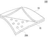
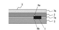
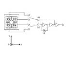
図3は、本発明の第1の実施の形態にかかる通信装置100の外観構成を示す図である。この通信装置100においては、複数の通信素子200が2枚の導電層16および18によって挟持されている。各通信素子200は、この2枚の導電層16および18に電気的に接続される。導電層16および18は、単層構造を有していても、また多層構造を有していてもよく、この例では二次元的に一面に広がった構成を有している。図3では、通信素子200が挟持されていることを説明するために、導電層16と導電層18とを開いた状態が示されている。 FIG. 3 is a diagram illustrating an external configuration of the
例えば、本発明による通信装置100をロボットの表面を覆う人工皮膚として応用する場合、導電層16および18は導電性のゴム材料により形成されることが好ましい。可撓性のあるゴム材料で人工皮膚を形成することにより、この人工皮膚はロボットの動作に合せて自在に伸縮することが可能となる。また、個別配線が存在せず、伸縮性のある導電層16および18を介して信号を伝達するため、断線などにより通信機能に障害が生じる可能性を低減し、安定した通信機能を実現することも可能となる。また、本発明による通信装置100を回路基板として応用する場合、導電層16および18を導電性のゴム材料で形成することによって、フレキシブルな回路基板を実現することも可能となる。 For example, when the
各通信素子200は通信機能以外に、さらに他の機能を有していてもよい。通信装置100をロボットの人工皮膚として応用する場合には、通信素子200のいくつかが触覚センサとしての機能も有し、外部から受けた刺激を検出した後、他の通信素子と協同して検出した信号を目的の通信素子まで伝達する。また通信装置100を基板の実装技術として応用する場合には、通信素子200が、例えばLSIやメモリなどの回路素子としての機能を有してもよい。このように、本明細書において「通信装置」は少なくとも通信機能を有する装置の意味で用い、これに付加した他の機能、例えば人工皮膚としてのセンサ機能や電子回路としての演算機能などを有してもよいことは、当業者に理解されるところである。 Each
図4は、通信素子200の機能ブロック図である。通信素子200は、通信部50、処理部60およびメモリ70を備える。通信部50は、導電層16および18(図3参照)を介して、他の通信素子との間で信号の送受を行う。処理部60は、通信素子200の通信機能を制御する。具体的に処理部60は、周囲の信号の監視、受信信号の解析や、送信信号の生成および信号の送信タイミングなど他の通信素子200との間の信号伝達に関する行為を自発的に行うことが好ましい。また、処理部60は、センサ機能や演算機能など通信機能以外の他の機能を実現してもよい。メモリ70は、通信機能や他の機能を実現するために必要な情報を予め記憶し、また必要に応じて順次記憶していく。 FIG. 4 is a functional block diagram of the
図5は、通信装置100の断面を示し、局所的通信を実現する通信デバイスの構造の一例を説明するための図である。本明細書において「通信デバイス」は、通信機能を実現するための構造の意味で用い、具体的には有効通信距離内に存在する他の通信素子に対して信号を伝達する構造を示す。 FIG. 5 is a diagram illustrating a cross-section of the
この例において通信デバイスは、第1信号層20および第2信号層30と、これらの層に電気的に接続する通信素子200を備える。第1信号層20および第2信号層30は絶縁されており、第2信号層30は接地されたグランド層であってもよい。第1信号層20および第2信号層30は導電層である。この通信デバイスにおいて、有効通信距離は第1信号層20または第2信号層30の抵抗と、第1信号層20と第2信号層30の間の容量に基づいて定められ、第1信号層20または第2信号層30に電荷を放出することにより信号を発信する。各通信素子はコンデンサを有しており、放出された電荷は有効通信距離内に配置されている周辺の通信素子のコンデンサに蓄積される。周辺の通信素子は、第1信号層20と第2信号層30の間の電圧変化により信号を認識する。このように図5に示した通信デバイスはコンデンサを駆動するように振る舞い、この通信デバイスを「電荷蓄積型」の通信デバイスと呼んでもよい。なおこの呼び名は、説明の便宜上、後述する「電流拡散型」の通信デバイスと区別するために名付けたものであって、図5に示した通信デバイスの特性および構成が、この呼び名の意味により限定されるものではない。In this example, the communication device includes a
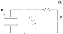
図6は、電荷蓄積型の通信デバイスが信号を発信する原理を説明するための図である。図6(a)は、駆動用コンデンサ34bを充電する通信素子200の状態を示す。主コンデンサ34aは、通信素子200全体を駆動するために必要な電荷を蓄積し、駆動用コンデンサ34bは、通信層36を駆動するために必要な電荷を蓄積する。通信層36は、第1信号層20および第2信号層30(図5参照)を模式的に表したものである。駆動用コンデンサ34bの充電時には、スイッチ32aを開き、スイッチ32bを閉じる。なお、各スイッチ32aおよび32bは、処理部(図4参照)により所定のタイミングで開閉される。なお本方式により、後述の電流拡散型の通信デバイスを駆動することも可能である。 FIG. 6 is a diagram for explaining the principle that a charge storage type communication device transmits a signal. FIG. 6A shows a state of the
図6(b)は、駆動用コンデンサ34bを放電する通信素子200の状態を示す。駆動用コンデンサ34bの放電時には、スイッチ32aを閉じ、スイッチ32bを開く。この通信デバイスは、駆動用コンデンサ34bの電荷を通信層36に放電することによって信号を発信する。1ビットの送信ごとに、主コンデンサ34aから駆動用コンデンサ34bに電荷を移動し、駆動用コンデンサ34bの電荷を通信層36に放電することによって、連続した通信を実現することが可能となる。 FIG. 6B shows a state of the
通信層36の面抵抗率がρ[Ω]、単位面積あたりの容量がC[F/m2]である場合、角周波数ω[rad/s]の信号の有効伝達距離(有効通信距離)D[m]は、When the surface resistivity of the

特に連鎖伝達型の通信方式においては、近傍の通信素子200との間で信号の送受を行うことができればよいため、有効通信距離を可能な限り短く設定することが好ましい。例えば通信装置100内において、通信素子200間の距離が10cm以内となるような密度で複数の通信素子200が配置されている場合には、有効通信距離が10cm程度となるように通信層36の抵抗および容量を設定することが好ましい。有効通信距離を短く設定することによって、他の通信素子200への干渉や無用な電力消費を低減することが可能となる。 In particular, in the chain transmission type communication method, it is only necessary that signals can be transmitted to and received from
以上の原理を数式を用いて説明する。説明の簡単のため、1次元問題とし、原点に存在する微小電極に電圧V
V=V0exp(jωt)
が印加されたとすると、位置xにおける電圧Vは、
V = V0 exp (jωt)
Is applied, the voltage V at position x is
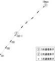
図7は、V/V0の実部を縦軸、x/Dを横軸とするグラフであって、電荷蓄積型の通信デバイスにおける電圧と通信距離の関係を示す図である。原点から離れるにつれ、電圧の振幅は指数関数的に減少するため、有効通信距離Dを大きく越える距離への影響は無視できることが分かる。したがって、この有効通信距離Dを通信素子200の密度に応じて好適に設定することにより、効率よい通信を実現することが可能となる。FIG. 7 is a graph having the real part of V / V0 as the vertical axis and x / D as the horizontal axis, and shows the relationship between the voltage and the communication distance in the charge storage type communication device. As the distance from the origin increases, the amplitude of the voltage decreases exponentially, so that it can be understood that the influence on the distance greatly exceeding the effective communication distance D is negligible. Therefore, efficient communication can be realized by suitably setting the effective communication distance D according to the density of the
図8は、通信装置100の断面を示し、局所的な通信を実現する通信デバイスの構造の別の例について説明するための図である。この通信デバイスは、スイッチング動作によって第1信号層20と第2信号層30の間を導通させ、その電圧降下によって信号を発信し、この通信デバイスを「電流拡散型」の通信デバイスと呼んでもよい。なおこの呼び名は、説明の便宜上、前述した「電荷蓄積型」の通信デバイスと区別するために名付けたものであって、図8に示す通信デバイスの特性および構成が、この呼び名の意味により限定されるものではない。FIG. 8 is a diagram illustrating a cross section of the
図8(a)は、電流拡散型の通信デバイスの構造の一例を示す図である。この通信デバイスは、第1信号層20および第2信号層30と、これらの層に電気的に接続する通信素子200を備える。第2信号層30は接地されたグランド層であってもよい。第1信号層20および第2信号層30は、これらの層よりも高い抵抗値を有する高抵抗層40によって導通される。具体的には、通信素子200の周囲に高抵抗層40が設けられ、この通信素子200および高抵抗層40とが第1信号層20および第2信号層30に挟持される。高抵抗層40の抵抗値を第1信号層20および第2信号層30の抵抗値と比較して適切に設定するか、または通信素子200の2つの電極間を素子内部において適切な抵抗値で常時導通させることにより、通信素子200内において第1信号層20および第2信号層30をスイッチング動作により導通させた場合に、発信した信号が遠くまで広がらず、有効通信距離を近傍の通信素子までの短い距離に設定することが可能となる。 FIG. 8A is a diagram illustrating an example of the structure of a current spreading type communication device. The communication device includes a
図8(b)は、電流拡散型の通信デバイスの構造の別の例を示す図である。この通信デバイスは、第1信号層20および第2信号層30と、これらの層に電気的に接続する通信素子200を備える。第2信号層30は接地されたグランド層であってもよい。第1信号層20および第2信号層30は絶縁されており、第1信号層20には、第1信号層20よりも高い抵抗値を有する高抵抗層42が電気的に接続され、この高抵抗層42には、通信素子200に電力を供給する電源層44が電気的に接続されている。具体的には、第1信号層20上に、高抵抗層42および電源層44とがこの順に積層されている。第1信号層20および第2信号層30が絶縁されることにより、これらの層間において電流が定常的に流れる状態を回避することができる。第2信号層30と電源層44は、その抵抗値が非常に小さくなるように形成される。 FIG. 8B is a diagram illustrating another example of the structure of the current spreading communication device. The communication device includes a
第1信号層20の抵抗は、有効通信距離に基づいて設定される。すなわち第1信号層20の抵抗を高抵抗層42との関係において適切に定めることによって、電流の拡散範囲を設定することが可能となる。なお単位面積あたりで、高抵抗層42の縦方向インピーダンスが、第1信号層20と第2信号層30および電源層44との間の静電容量によるインピーダンスZよりも大きい場合には、拡散距離は第1信号層20の抵抗とインピーダンスZによって決まる。 The resistance of the
以上の原理を数式を用いて説明する。説明の簡単のため、第1信号層20の厚みは無視できるほど薄いものとする。第1信号層20と電源層44の間の静電容量と、第1信号層20と第2信号層30の間の静電容量の和がC[F/m2]、高抵抗層42の抵抗率および厚さがそれぞれη[Ωm]およびd[m]、第1信号層20の面抵抗がρ[Ω]、角周波数がω[rad/s]である場合、第1信号層20の電位V(x,y)の非定常成分は、The above principle will be described using mathematical expressions. For simplicity of explanation, the thickness of the
ηd<1/ωC (電流拡散条件)
の場合には、1/ηdの寄与が支配的となり、電流拡散型の信号伝達を実現することができる。これを1次元問題として考えると、原点に存在する微小電極に印加される電圧V
V=V0exp(jωt)
に対して、位置xにおける電圧Vは、
ηd <1 / ωC (Current diffusion condition)
In this case, the contribution of 1 / ηd becomes dominant, and current spreading type signal transmission can be realized. Considering this as a one-dimensional problem, the voltage V applied to the microelectrode existing at the origin.
V = V0 exp (jωt)
On the other hand, the voltage V at the position x is
この数式に含まれる各要素、例えば第1信号層20の抵抗を適宜設定することにより、所望の有効通信距離を得ることが可能となる。 It is possible to obtain a desired effective communication distance by appropriately setting each element included in this mathematical formula, for example, the resistance of the
図8(c)は、電流拡散型の通信デバイスの構造の別の例を示す図である。この通信デバイスは、第1信号層20および第2信号層30と、これらの層に電気的に接続する通信素子200を備える。第1信号層20および第2信号層30は絶縁されており、第1信号層20には、第1信号層20よりも高い抵抗値を有する高抵抗層42が電気的に接続され、この高抵抗層42には、通信素子200に電力を供給する電源層44が電気的に接続されている。同様に、第2信号層30には、第2信号層30よりも高い抵抗値を有する高抵抗層46が電気的に接続され、この高抵抗層46には、通信素子200に電力を供給する電源層48が電気的に接続されている。具体的には、第1信号層20の上面に、高抵抗層42および電源層44とがこの順に積層されており、第2信号層30の下面に、高抵抗層46および電源層48とがこの順に積層されている。図8(b)に示した通信デバイスは、通信素子200の片面のみに積層構造を形成していたが、図8(c)のように、通信素子200の両面に上下対称な積層構造を形成してもよい。各層の構成および特性については、図8(b)において説明したとおりである。 FIG. 8C is a diagram illustrating another example of the structure of the current spreading type communication device. The communication device includes a
図9は、電流拡散型の通信デバイスが信号を発信する原理を説明するための図である。主コンデンサ34は、通信素子200全体を駆動するために必要な電荷を蓄積する。通信層36は、第1信号層20および第2信号層30(図8参照)を模式的に表したものである。この通信素子200は、スイッチ32のスイッチング動作により電極間インピーダンスを変化させ、信号を発信する。なおスイッチ32は処理部(図4参照)により所定のタイミングで開閉される。なお本方式で、電荷蓄積型の通信デバイスを駆動することも可能である。 FIG. 9 is a diagram for explaining the principle that a current spreading communication device transmits a signal. The
スイッチ32を閉じると、第1信号層20および第2信号層30とが短絡する。その結果、第1信号層20と第2信号層30の間に電圧降下が生じ、近傍の通信素子がその影響を受け、この電圧降下を信号として認識する。前述のとおり、連鎖伝達型の通信方式においては、この電圧降下の影響は、近傍の通信素子に伝達されればよく、遠くに位置する通信素子にまで伝達される必要はない。有効通信距離を近傍に位置する他の通信素子の距離程度に設定することにより、電力消費を少なくすることができ、また他の通信素子との干渉を低減することも可能となる。 When the
次に、通信素子200に電力を供給する方法について説明する。その一つの方法として、図8(b)を参照して、通信デバイスを多層構造に形成することにより、電源層44から電力を通信素子200に供給することが可能である。通信素子200と電源層44との間に高抵抗層42を介在させることにより、電荷が低抵抗である電源層44全面に供給されるため、通信装置100全体に分布している通信素子200のコンデンサを安定して充電し、且つ通信距離を適切な距離まで拡大するとともに信号伝達の際の電力消費を抑えることができる。 Next, a method for supplying power to the
図10は、通信素子に電力を供給する別の構成を示す図である。この例では、通信装置100に電力供給線52と給電点54とが形成され、電力が電力供給線52から給電点54を介して、通信装置100内の通信素子に供給される。このときの電力供給方法として、例えば、通信素子の信号送受信期間と充電期間とを時間的に分けてもよい。ある通信素子が信号を送信する際には、周囲の素子の端子間インピーダンスを高く保ち、電力を供給する際には、全ての素子の信号送信を停止して、通信素子のコンデンサに一斉に充電する。特に、通信素子が第1信号層および第2信号層からなる2層構造を有し、電源層を含む多層構造をとらない場合には、このような電力供給線52を形成してもよい。 FIG. 10 is a diagram illustrating another configuration for supplying power to the communication element. In this example, a
以上、図5から図10を通じて、通信デバイスの具体的な構造について説明したが、通信デバイスは上述した構造に限らず、周辺の通信素子との間で信号を送受できるものであればよい。以下に、局所的な通信を行う通信デバイスを用いた連鎖伝達型の通信方式の詳細について説明する。 The specific structure of the communication device has been described above with reference to FIGS. 5 to 10. However, the communication device is not limited to the structure described above, and any communication device may be used as long as it can transmit and receive signals to and from surrounding communication elements. Details of the chain transmission type communication method using a communication device that performs local communication will be described below.
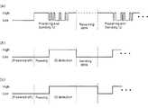
本実施の形態において、連鎖伝達型の通信アルゴリズムには「論理波動伝播モード」と、「アドレス連鎖伝達モード」とが存在する。論理波動伝播モードは、発信元の通信素子から全ての通信素子に信号をブロードキャストする通信アルゴリズムであり、アドレス連鎖伝達モードは、経路を定めて、発信元の通信素子から目的地である通信素子まで経路に沿って信号を伝達する通信アルゴリズムである。まず、論理波動伝播モードについて説明する。 In the present embodiment, the chain transmission type communication algorithm includes a “logic wave propagation mode” and an “address chain transmission mode”. The logic wave propagation mode is a communication algorithm that broadcasts a signal from the source communication element to all the communication elements. The address chain transmission mode determines the route from the source communication element to the destination communication element. It is a communication algorithm that transmits a signal along a path. First, the logic wave propagation mode will be described.
図11は、通信装置において論理波動伝播モードにより信号が伝播する状態を説明するための図である。図中、小さな円は通信素子を示し、中央の黒塗りの円は、信号の発信元である通信素子を示す。通信素子を囲んでいる同心円は、信号を受信した通信素子の領域を示す。 FIG. 11 is a diagram for explaining a state in which a signal propagates in the logic wave propagation mode in the communication device. In the figure, a small circle indicates a communication element, and a black circle at the center indicates a communication element that is a signal source. Concentric circles surrounding the communication element indicate the area of the communication element that has received the signal.
論理波動伝播モードにおいては、信号待機中、全ての通信素子が周囲の信号を監視する。信号を受信した通信素子は、その信号をメモリに格納し、確率1/nで同一の信号系列を送信する。送信確率1/nは、確実に信号が通信装置全体に伝播するように予め設定される。各信号系列は「信号ID」を有しており、通信素子が同一の信号IDをもつ信号を受信した場合には、その信号の転送を行わないことが好ましい。以上の動作を各通信素子が実行することにより、任意の通信素子から発生した論理波動伝播信号が、図示されるようにほぼ同心円状に広がっていき、通信装置全体に伝達されることになる。 In the logic wave propagation mode, all communication elements monitor surrounding signals during signal standby. The communication element that has received the signal stores the signal in the memory and transmits the same signal sequence with a probability of 1 / n. The
次に、アドレス連鎖伝達モードについて説明する。 Next, the address chain transmission mode will be described.
図12は、アドレス連鎖伝達モードにおける通信素子の階層構造を説明するための図である。アドレス連鎖伝達モードにおいては、複数の通信素子が、通信の管理機能の低いものから順に1次からN次までの階層に分類される。2≦M≦Nとした場合、M次通信素子の配置密度は、(M−1)次通信素子の配置密度よりも低く設定される。M次通信素子は、自身から所定の範囲内に配置された(M−1)次通信素子を管轄し、またM次通信素子は、(M−1)次通信素子が有する通信管理に必要な機能を少なくとも有している。ここで管轄するとは、他の通信素子のIDの管理などを行うことを意味する。便宜上、管轄する側の通信素子を「親素子」、管轄される側の通信素子を「子素子」と呼んでもよい。通信処理を行う際、M次通信素子は、M次の階層の通信素子として機能するだけではなく、1次から(M−1)次の階層の通信素子としても機能することができる。M次通信素子がある階層の通信素子として機能する場合には、その階層において設定された所定の範囲内に配置された1階層下の通信素子を管轄することになる。M次通信素子は、管轄下にある(M−1)次通信素子が管轄する(M−2)次通信素子についても管轄してよいが、(M−2)次通信素子について管轄していない場合であっても(M−1)次通信素子に対して適宜問い合わせを行うことにより、この(M−2)次通信素子を把握することが可能である。 FIG. 12 is a diagram for explaining a hierarchical structure of communication elements in the address chain transfer mode. In the address chain transmission mode, a plurality of communication elements are classified into a hierarchy from the first order to the Nth order in order from the lowest communication management function. When 2 ≦ M ≦ N, the arrangement density of the Mth order communication elements is set lower than the arrangement density of the (M−1) th order communication elements. The Mth order communication element has jurisdiction over the (M-1) th order communication element disposed within a predetermined range from itself, and the Mth order communication element is necessary for the communication management of the (M-1) th order communication element. Has at least a function. The jurisdiction here means managing IDs of other communication elements. For convenience, the communication element on the jurisdiction side may be called the “parent element”, and the communication element on the jurisdiction side may be called the “child element”. When performing communication processing, the M-th order communication element not only functions as a communication element in the M-th layer, but can also function as a communication element in the first to (M-1) th layers. In the case where the Mth order communication element functions as a communication element in a certain hierarchy, the communication element one hierarchy below is arranged within a predetermined range set in that hierarchy. The M-th order communication element may have jurisdiction over the (M-1) next communication element under the jurisdiction of the (M-1) next communication element, but (M-2) it does not have jurisdiction over the next communication element. Even if it is a case, it is possible to grasp | ascertain this (M-2) next communication element by making an inquiry suitably with respect to the (M-1) next communication element.
連鎖伝達型の通信装置において、全ての通信素子は、その有効通信距離を、周辺に配置された他の通信素子と局所的な通信を行える程度に設定されている。素子間隔が大体10cmとなるように通信素子が分散して配置されている場合には、通信素子の有効通信距離も10cm程度に設定される。 In the chain transmission type communication device, all communication elements have their effective communication distances set so that local communication can be performed with other communication elements arranged in the vicinity. When communication elements are distributed and arranged so that the element interval is approximately 10 cm, the effective communication distance of the communication elements is also set to about 10 cm.
このときの各階層における通信素子の配置間隔について説明すると、1次通信素子は大体10cm間隔で配置されており、M次通信素子の配置間隔は(M−1)次通信素子の配置間隔の数倍程度となるように配置されるのが好ましい。したがって、2次通信素子の配置間隔は、数10cm程度となる。なお、この配置間隔は厳密である必要はなく、大体の間隔が把握されていればよい。1次通信素子は最も高密度に配置されて、その周囲の一定の距離までに存在する他の通信素子に信号を伝達し、本通信装置における信号伝達の基本素子として機能する。なお、前述のように2次以上の通信素子であっても、信号の連鎖伝達時には1次通信素子として機能することができる。通信装置における信号の転送を考えた場合に、1次通信素子は、他の通信素子を管轄する機能を有しなくてよい。なお、後述するが、例えば1次通信素子の周辺にセンサなどが配置される場合には、1次通信素子は、これらのセンサを管轄する機能を有することになる。 The arrangement intervals of the communication elements in each layer at this time will be described. The primary communication elements are arranged at intervals of about 10 cm, and the arrangement intervals of the Mth order communication elements are (M-1) the number of arrangement intervals of the next communication elements. It is preferable to arrange so as to be about double. Accordingly, the arrangement interval of the secondary communication elements is about several tens of centimeters. Note that this arrangement interval does not need to be strict, and it is only necessary to grasp an approximate interval. The primary communication elements are arranged at the highest density, transmit signals to other communication elements existing up to a certain distance around the primary communication elements, and function as basic elements for signal transmission in this communication apparatus. As described above, even a secondary or higher order communication element can function as a primary communication element at the time of signal chain transmission. When considering the transfer of signals in the communication device, the primary communication element does not have to have a function of controlling other communication elements. As will be described later, for example, when a sensor or the like is disposed around the primary communication element, the primary communication element has a function of controlling these sensors.
まず、通信装置において階層構造の最上位に一つのN次通信素子が存在する場合の通信アルゴリズムについて説明する。このアルゴリズムによると、送信元と送信先の通信素子の階層構造の上位に共通の通信素子が存在するとき、その上位の通信素子が送信元から信号を受け取り、送信先までの経路を作成して信号を転送する。通信装置において階層構造最上位のN次通信素子が一つしか存在しない場合には、このN次通信素子は少なくとも上位の共通の通信素子となりうるため、この通信アルゴリズムが有効に機能することが明らかである。 First, a communication algorithm in the case where one Nth order communication element exists at the top of the hierarchical structure in the communication device will be described. According to this algorithm, when there is a common communication element at the upper level of the hierarchical structure of the source and destination communication elements, the higher-level communication element receives a signal from the source and creates a path to the destination. Transfer the signal. When there is only one highest-order Nth order communication element in the hierarchical structure in the communication device, this Nth order communication element can be at least a higher order common communication element, and it is clear that this communication algorithm functions effectively. It is.
M次通信素子が信号の送信元であるとすると、送信先が自分の階層構造の下位に所属する場合には、自分で送信先までの経路を作成して信号を送信する。一方、送信先が自分の階層構造の下位に所属しない場合には、自分の親素子である(M+1)次通信素子に信号を送信する。この親素子は、送信先が自分の階層構造の下位に所属しているか否かを確認して、所属する場合には送信先までの経路を作成し、所属しない場合にはさらに自分の親素子である(M+2)次通信素子に信号を送信する。この作業を繰り返して、最上位のN次通信素子まで信号が伝達された場合には、N次通信素子が、送信先までの経路を作成する。この通信アルゴリズムによると、あるM次通信素子が他のM次通信素子の子素子に信号を送信する場合、共通の親素子である(M+1)次通信素子に一旦信号を送信して、この(M+1)次通信素子が、他のM次通信素子に転送するという手法をとる。 Assuming that the M-th order communication element is a signal transmission source, if the transmission destination belongs to the lower level of its own hierarchical structure, it creates a route to the transmission destination by itself and transmits the signal. On the other hand, when the transmission destination does not belong to the lower level of its own hierarchical structure, a signal is transmitted to the (M + 1) next communication element that is its parent element. This parent element checks whether or not the destination belongs to the lower level of its own hierarchical structure. If it belongs, it creates a route to the destination, and if it does not belong, it further adds its own parent element. A signal is transmitted to the next communication element (M + 2). When this operation is repeated and a signal is transmitted to the highest order Nth order communication element, the Nth order communication element creates a route to the transmission destination. According to this communication algorithm, when a certain Mth order communication element transmits a signal to a child element of another Mth order communication element, a signal is once transmitted to the (M + 1) th order communication element which is a common parent element, and this ( M + 1) A method in which the next communication element transfers to another Mth order communication element is adopted.
一方、最上位であるN次通信素子が複数存在する場合には、送信元と送信先の通信素子が、一つのN次通信素子における階層内に所属しない場合も生じうる。このとき、N次通信素子が、自身の階層内に送信先の通信素子が存在しないことを確認すると、別のN次通信素子に対して調査要求を送信し、送信先の通信素子を階層下とするN次通信素子を探索する。探索の結果、送信元の上位素子であるN次通信素子は、送信先の上位素子であるN次通信素子までの経路を定め、その経路に沿って信号を送信する。この通信アルゴリズムは、最上位のN次においてだけでなく、下位の通信素子の階層において利用されてもよい。すなわち、この通信アルゴリズムによると、あるM次通信素子が他のM次通信素子の子素子に信号を送信する場合、M次通信素子が(M+1)次通信素子を介することなく、他のM次通信素子を直接探索して、そのM次通信素子に信号を送信することができる。信号の伝達効率を高めるために、M次通信素子は、適当な範囲において存在する他のM次通信素子のIDや経路などをキャッシュ等に記憶しておいてもよい。なお、送信元の上位素子であるN次通信素子は、送信先までの経路を設定すると、図13に示す送信パケットを生成して信号を送信する。 On the other hand, when there are a plurality of highest-order N-th order communication elements, the source and destination communication elements may not belong to a hierarchy in one N-th order communication element. At this time, when the N-th order communication element confirms that the destination communication element does not exist in its own hierarchy, it transmits an investigation request to another N-order communication element, Nth order communication elements are searched. As a result of the search, the N-th order communication element that is the higher-order element of the transmission source determines a route to the N-th order communication element that is the higher-order element of the transmission destination, and transmits a signal along the route. This communication algorithm may be used not only in the highest order N but also in the lower communication element hierarchy. That is, according to this communication algorithm, when a certain Mth order communication element transmits a signal to a child element of another Mth order communication element, the Mth order communication element does not go through the (M + 1) th order communication element, and other Mth order communication elements. A communication element can be searched directly and a signal can be transmitted to the Mth order communication element. In order to increase the signal transmission efficiency, the Mth order communication element may store the IDs and paths of other Mth order communication elements existing in an appropriate range in a cache or the like. Note that the N-order communication element, which is a higher-order element of the transmission source, generates a transmission packet shown in FIG. 13 and transmits a signal when a path to the transmission destination is set.
図13は、送信パケットの構成の一例を示す図である。この送信パケットは、信号の転送(伝達)に使われるものであって、
(1) コマンド
(2) 受信ID
(3) 送信先ID
(4) 送信元ID
(5) 階層数
(6) N次階層内連鎖数
(7) N次階層内経路データ
(8) 1次階層内連鎖数
(9) 1次階層内経路データ
(10) 送信データ
のデータ項目を有している。FIG. 13 is a diagram illustrating an example of a configuration of a transmission packet. This transmission packet is used for signal transfer (transmission).
(1) Command
(2) Receive ID
(3) Destination ID
(4) Sender ID
(5) Number of layers
(6) Number of chains in the Nth hierarchy
(7) Route data in Nth layer
(8) Number of chains in the primary hierarchy
(9) Route data in the primary hierarchy
(10) It has a data item of transmission data.
この送信パケットのことを「転送パケット」と呼んでもよい。省略しているが、この送信パケットには、2次から(N−1)次までの各階層内の連鎖数および経路データも含まれる。以下、各データ項目の内容を説明する。この送信パケットは、N次通信素子が複数存在する環境において、送信元の階層上位のN次通信素子と送信先の階層上位のN次通信素子とが異なる場合に、N次通信素子により生成されるものと説明した。なお、送信元の通信素子と送信先の通信素子とが一つの(N+1)次通信素子の階層に所属する場合にも、この(N+1)次通信素子が、図13に示される送信パケットを生成する。 This transmission packet may be referred to as a “forwarding packet”. Although omitted, this transmission packet includes the number of chains in each layer from the second order to the (N-1) th order and the route data. Hereinafter, the contents of each data item will be described. This transmission packet is generated by the Nth order communication element when the Nth order communication element at the higher level of the transmission source and the Nth order communication element at the higher level of the transmission destination are different in an environment where there are a plurality of Nth order communication elements. Explained. Even when the source communication element and the destination communication element belong to the hierarchy of one (N + 1) th order communication element, this (N + 1) th order communication element generates the transmission packet shown in FIG. To do.
コマンドは、送信パケットの処理方法を指示するものである。上の例は信号を転送するための転送パケットであるため、このコマンドには、転送指示に関するコードなどが記述される。受信IDは、この送信パケットを次に受信するべき通信素子のIDである。送信先IDは、送信パケットの最終目的地である通信素子のIDである。送信元IDは、データ信号の発信元である通信素子のIDである。階層数は、信号伝達に携わる通信素子の階層の数であり、この項目には「N」が記述される。 The command instructs the processing method of the transmission packet. Since the above example is a transfer packet for transferring a signal, a code related to a transfer instruction is described in this command. The reception ID is an ID of a communication element that should receive this transmission packet next. The transmission destination ID is the ID of the communication element that is the final destination of the transmission packet. The transmission source ID is an ID of a communication element that is a transmission source of the data signal. The number of layers is the number of layers of communication elements involved in signal transmission, and “N” is described in this item.
N次階層内連鎖数は、最終目的地までの経路に存在するN次通信素子の連鎖数であり、N次階層内経路データは、最終目的地までの経路に存在するN次通信素子のIDおよび順序に関するデータである。具体的にN次階層内経路データは、最終目的地である通信素子を管轄するN次通信素子へ至るために、どのような順でN次通信素子を経由すればよいかを順にそのIDを並べて記述したものである。経由地であるN次通信素子は、このパケットを受け取ると、自分のIDをN次階層内経路データから削除し、N次階層内連鎖数を1だけ減らす。 The number of chains in the Nth layer is the number of chains of Nth order communication elements existing in the route to the final destination, and the path data in the Nth layer is the ID of the Nth order communication element existing in the route to the final destination. And order data. Specifically, the route data in the Nth layer is assigned with the ID in order of what order the Nth order communication device should be routed to reach the Nth order communication device that controls the communication device that is the final destination. It is described side by side. Upon receiving this packet, the Nth order communication element that is a transit point deletes its own ID from the Nth order layer route data and reduces the Nth order layer chain number by one.
同様に、2≦M≦Nとしたとき、(M−1)次階層内経路データは、次のM次以上の通信素子に至るために、どのような順で(M−1)次通信素子を経由すればよいかを順にそのIDを並べて記述したものであり、(M−1)次階層内連鎖数はそのIDの個数である。具体的に1次階層内連鎖数は、次の2次以上の通信素子までの経路に存在する1次の階層における通信素子の連鎖数であり、1次階層内経路データは、次の2次以上の通信素子までの経路に存在する1次通信素子のIDおよび順序に関するデータである。次の2次以上の通信素子がない場合には、1次階層内経路データは、最終目的地までの経路に存在する1次通信素子のIDおよび順序に関するデータとなる。送信データは、伝達すべきデータである。 Similarly, when 2 ≦ M ≦ N, the (M−1) next-layer path data reaches the next M-th or higher order communication element. The IDs are listed in order as to whether or not to pass through, and (M-1) the number of chains in the next hierarchy is the number of the IDs. Specifically, the number of chains in the primary hierarchy is the number of chains of communication elements in the primary hierarchy existing in the path to the next secondary or higher communication element, and the path data in the primary hierarchy is the next secondary This is data relating to the ID and order of the primary communication elements existing on the path to the communication element. When there is no communication element of the next secondary or higher, the route data in the primary hierarchy is data relating to the ID and order of the primary communication elements existing in the route to the final destination. Transmission data is data to be transmitted.
図14は、各階層内の経路データを概念的に示した図である。この例では、階層数を3に設定し、左端の3次通信素子から右端の3次通信素子まで信号を送信する場合を仮定する。 FIG. 14 is a diagram conceptually showing route data in each layer. In this example, it is assumed that the number of layers is set to 3 and a signal is transmitted from the leftmost tertiary communication element to the rightmost tertiary communication element.
3次の階層において、信号は左端の3次通信素子から中央の3次通信素子を経由して右端の3次通信素子に伝達される。したがって3次階層内経路データは、中央と右端の3次通信素子のIDをこの順に並べて構成される。 In the tertiary hierarchy, the signal is transmitted from the leftmost tertiary communication element to the rightmost tertiary communication element via the central tertiary communication element. Accordingly, the path data in the tertiary hierarchy is configured by arranging the IDs of the center and rightmost tertiary communication elements in this order.
2次の階層において、信号が左端の3次通信素子から中央に位置する次の3次通信素子に中継される場合に、信号はこれら3次通信素子間に存在する3つの2次通信素子を経由する。したがって、2次階層内経路データは、3つの2次通信素子のIDと、中央の3次通信素子のIDとを左から順に並べて構成される。 In the secondary hierarchy, when a signal is relayed from the leftmost tertiary communication element to the next tertiary communication element located in the center, the signal has three secondary communication elements existing between these tertiary communication elements. Via. Accordingly, the path data in the secondary hierarchy is configured by arranging the IDs of the three secondary communication elements and the ID of the central tertiary communication element in order from the left.
1次の階層において、信号が左端の3次通信素子から次の2次通信素子に中継される場合に、信号はこれらの通信素子間に存在する3つの1次通信素子を経由する。したがって、1次階層内経路データは、3つの1次通信素子のIDと、次の2次通信素子のIDとを左から順に並べて構成される。 In the primary hierarchy, when a signal is relayed from the leftmost tertiary communication element to the next secondary communication element, the signal passes through the three primary communication elements existing between these communication elements. Accordingly, the path data in the primary hierarchy is configured by arranging the IDs of three primary communication elements and the ID of the next secondary communication element in order from the left.
M次通信素子は、自身が管轄する(M−1)次通信素子までの経路を、他の(M−1)次通信素子を経由する経路としてメモリに記憶する。またM次通信素子は、自身から所定の範囲内に配置された他のM次通信素子までの経路を、(M−1)次通信素子を経由する経路としてメモリに記憶する。ここで、M次通信素子は、2次から(M−1)次の通信素子としても機能することができ、ある階層の通信素子として機能する場合には、その階層において設定される所定の範囲内に配置された1階層下の通信素子を管轄する。例えば2次通信素子として機能する場合には、M次通信素子が、2次通信素子として管轄する全ての1次通信素子までの経路を、1次通信素子を経由する経路としてメモリに記憶している。具体的には、ある1次通信素子までの経路は、複数の1次の通信素子を経由した経路として定められる。図14を参照して、左端の3次通信素子は、3次通信素子として2次通信素子を管轄する場合には、これら2次通信素子および隣の中央の3次通信素子までの経路を把握し、また2次通信素子として1次通信素子を管轄する場合には、これら1次通信素子および隣の2次通信素子までの経路を把握している。 The Mth order communication element stores the path to the (M-1) th order communication element that it has jurisdiction in the memory as a path that passes through the other (M-1) th order communication elements. Further, the Mth order communication element stores a path from itself to another Mth order communication element arranged in a predetermined range in the memory as a path via the (M-1) th order communication element. Here, the Mth order communication element can also function as a secondary to (M-1) th order communication element. When the Mth order communication element functions as a communication element of a certain level, a predetermined range set in that level The communication element one level below is in charge. For example, when functioning as a secondary communication element, the M-th order communication element stores the paths to all the primary communication elements that have jurisdiction as the secondary communication elements in the memory as paths that pass through the primary communication elements. Yes. Specifically, a route to a certain primary communication element is determined as a route via a plurality of primary communication elements. Referring to FIG. 14, when the tertiary communication element at the left end has jurisdiction over the secondary communication element as the tertiary communication element, the path to these secondary communication elements and the adjacent central tertiary communication element is grasped. In addition, when the primary communication element is controlled as the secondary communication element, the route to the primary communication element and the adjacent secondary communication element is grasped.
また逆に、(M−1)次通信素子は、自身を管轄するM次通信素子までの経路の少なくとも一部を、他の(M−1)次通信素子を経由する経路としてメモリに記憶する。すなわち、子素子は、他の子素子を経由して親素子へ向かう経路を認識している。 Conversely, the (M-1) next communication element stores at least a part of the path to the M order communication element having jurisdiction over itself in the memory as a path via another (M-1) next communication element. . That is, the child element recognizes a path toward the parent element via another child element.
データ信号の送信パケットには、最終目的地である通信素子に到達するために利用される各階層内の経路データが含まれ、この経路データは、信号の伝達に携わる各通信素子によって適宜更新される。M次通信素子は、(M−1)次の階層内経路データを設定する。 The transmission packet of the data signal includes route data in each layer used to reach the communication element that is the final destination, and this route data is appropriately updated by each communication element involved in signal transmission. The The M-th order communication element sets the (M-1) -th order hierarchical path data.
また送信パケットには、次に送信パケットを受け取るべき通信素子を特定する受信IDが含まれており、各通信素子は、この受信IDにより、この信号が自身に対するものであるか否かを判別する。通信素子は、この受信IDに基づいて送信パケットを受け取ると、次に送信パケットを受け取るべき通信素子の受信IDを設定して、送信パケットを発信する。経路データには、次に受け取るべき通信素子のIDが含まれており、通信素子は、経路データからこのIDを抽出して受信IDを設定する。このように各通信素子は、送信パケットを受け取ると、経路データを更新して、順次その送信パケットを転送していく。 The transmission packet includes a reception ID for specifying a communication element that should receive the transmission packet next. Each communication element determines whether or not the signal is for itself based on the reception ID. . When the communication element receives the transmission packet based on the reception ID, the communication element sets the reception ID of the communication element that should receive the transmission packet next, and transmits the transmission packet. The path data includes the ID of the communication element to be received next, and the communication element extracts the ID from the path data and sets the reception ID. As described above, when each communication element receives the transmission packet, it updates the route data and sequentially transfers the transmission packet.
図15は、アドレス連鎖伝達モードにおいて、送信元の通信素子からその親素子に信号を伝達する状況を説明するための説明図である。全ての通信素子は、自身を識別するためのIDを有する。このIDの設定方法については後述し、以下では、各通信素子がIDを有していることを前提として、信号伝達において、発信元から自身の上位の通信素子に信号を伝達する通信アルゴリズムについて説明する。ここでは通信に携わる通信素子のみを示すが、実際の通信装置では他の通信素子も分散して配置されていることに留意されたい。また、理解を容易にするために、階層数を3、すなわち3次通信素子が最高次として設定されている場合について説明する。以下では、具体的に、ID1の1次通信素子から別の1次通信素子まで信号を伝達する例について説明する。 FIG. 15 is an explanatory diagram for explaining a situation in which a signal is transmitted from the transmission source communication element to its parent element in the address chain transmission mode. All communication elements have an ID for identifying themselves. This ID setting method will be described later, and in the following, a communication algorithm for transmitting a signal from a transmission source to its own upper communication element in signal transmission on the assumption that each communication element has an ID will be described. To do. Here, only communication elements engaged in communication are shown, but it should be noted that other communication elements are also distributed in an actual communication apparatus. In order to facilitate understanding, a case will be described in which the number of layers is 3, that is, the tertiary communication element is set as the highest order. Below, the example which transmits a signal from the primary communication element of ID1 to another primary communication element is demonstrated concretely.
まず、1次通信素子(ID1)が、自分の親素子である2次通信素子(ID2−1)に信号を送信する。1次通信素子(ID1)は、他の1次通信素子を介して自分の親素子である2次通信素子(ID2−1)に至る経路の少なくとも一部をメモリに記憶している。ここでは、1次通信素子(ID1)から2次通信素子(ID2−1)に向かう経路が、1次通信素子(ID1)から1次通信素子(ID2)および1次通信素子(ID3)を中継して2次通信素子(ID2−1)に到達するように設定されており、1次通信素子(ID1)は、この経路のうち、直接信号を伝達することになる1次通信素子(ID2)を少なくとも認識していればよい。同様に、1次通信素子(ID2)も、自分の親素子である2次通信素子(ID2−1)に向かう経路の少なくとも一部を認識している。この経路は、1次通信素子(ID2)から1次通信素子(ID3)を中継して2次通信素子(ID2−1)に到達するように設定されている。1次通信素子(ID2)は、この経路のうち、直接信号を伝達することになる1次通信素子(ID3)を少なくとも認識していればよい。同様に、1次通信素子(ID3)は、直接2次通信素子(ID2−1)に信号を伝達することが可能であることを認識している。 First, the primary communication element (ID1) transmits a signal to the secondary communication element (ID2-1) which is its parent element. The primary communication element (ID1) stores in memory at least a part of a path leading to the secondary communication element (ID2-1) which is its parent element via another primary communication element. Here, the path from the primary communication element (ID1) to the secondary communication element (ID2-1) is relayed from the primary communication element (ID1) to the primary communication element (ID2) and the primary communication element (ID3). Thus, the primary communication element (ID2) is set to reach the secondary communication element (ID2-1), and the primary communication element (ID1) transmits the signal directly in this path. As long as it is recognized. Similarly, the primary communication element (ID2) also recognizes at least a part of the route toward the secondary communication element (ID2-1) which is its parent element. This route is set so that the primary communication element (ID2) is relayed from the primary communication element (ID2) to the secondary communication element (ID2-1). The primary communication element (ID2) only needs to recognize at least the primary communication element (ID3) that directly transmits a signal in this path. Similarly, the primary communication element (ID3) recognizes that a signal can be directly transmitted to the secondary communication element (ID2-1).
親素子である2次通信素子(ID2−1)に至る経路のうち、1次通信素子(ID1)が1次通信素子(ID2)のみを認識している場合、1次通信素子(ID1)は信号を1次通信素子(ID2)に伝達し、1次通信素子(ID2)は、この信号が親素子である2次通信素子(ID2−1)に伝達すべき信号であることを検出して、1次通信素子(ID3)に伝達する。同様に、1次通信素子(ID3)もこの信号を2次通信素子(ID2−1)に伝達する。このように、子素子が、親素子への伝達経路のうち、次に信号を伝達する同一階層の子素子のみを認識している場合には、信号を受け取った子素子が自身で認識する子素子宛てに信号の行き先を書き換え、信号を伝達する。 When the primary communication element (ID1) recognizes only the primary communication element (ID2) among the paths leading to the secondary communication element (ID2-1) which is the parent element, the primary communication element (ID1) is The signal is transmitted to the primary communication element (ID2), and the primary communication element (ID2) detects that the signal is to be transmitted to the secondary communication element (ID2-1) which is the parent element. To the primary communication element (ID3). Similarly, the primary communication element (ID3) also transmits this signal to the secondary communication element (ID2-1). In this way, when the child element recognizes only the child element of the same hierarchy that transmits the signal next in the transmission path to the parent element, the child element that the child element that has received the signal recognizes itself. The destination of the signal is rewritten to the element, and the signal is transmitted.
一方、1次通信素子(ID1)が親素子へ至る経路中の全ての1次通信素子のIDおよび順序を認識している場合には、1次通信素子(ID1)が経路中の1次通信素子のIDおよび順序を特定する信号パケットを生成し発信してもよい。1次通信素子(ID1)が2次通信素子(ID2−1)までの経路を設定するため、信号を中継する1次通信素子(ID2)および1次通信素子(ID3)の処理負担が軽減され、高速な通信を実現することが可能となる。 On the other hand, when the primary communication element (ID1) recognizes the IDs and order of all the primary communication elements in the path to the parent element, the primary communication element (ID1) performs the primary communication in the path. A signal packet specifying the ID and order of the elements may be generated and transmitted. Since the primary communication element (ID1) sets a route to the secondary communication element (ID2-1), the processing load on the primary communication element (ID2) and the primary communication element (ID3) that relay signals is reduced. High-speed communication can be realized.
2次通信素子(ID2−1)は信号を受け取ると、この信号の最終目的地である1次通信素子(例えば、ID17)が自身の管轄下にあるかどうかをメモリに記憶したテーブルを参照して調査する。2次通信素子は、自身の管轄下にある1次通信素子のIDおよび経路を全てメモリに記憶しており、送信先の通信素子が自身の管轄下にあれば、メモリからその経路を読み出して、信号を最終目的地に伝達する。 When the secondary communication element (ID2-1) receives the signal, the secondary communication element (ID2-1) refers to a table stored in the memory to determine whether the primary communication element (for example, ID17) which is the final destination of the signal is under its own jurisdiction. To investigate. The secondary communication element stores the ID and path of the primary communication element under its jurisdiction in the memory, and if the destination communication element is under its jurisdiction, the path is read from the memory. , Transmit the signal to the final destination.
最終目的地である1次通信素子(ID17)が自身の管轄下にない場合、2次通信素子(ID2−1)は、自身の親素子である3次通信素子(IDmax)に信号を転送する。2次通信素子(ID2−1)は自身の親素子への経路を予めメモリに記憶している。親素子との間における1次通信素子を中継する経路の持ち方は、上述したとおりである。このようにして、最高次である3次通信素子(IDmax)まで信号が送信される。3次通信素子(IDmax)は、1次通信素子(ID17)までの経路を設定して、信号を送信する。 When the primary communication element (ID17) that is the final destination is not under its jurisdiction, the secondary communication element (ID2-1) transfers a signal to the tertiary communication element (IDmax) that is its parent element. . The secondary communication element (ID2-1) stores a route to its parent element in the memory in advance. The way of holding the path for relaying the primary communication element to and from the parent element is as described above. In this way, the signal is transmitted to the tertiary communication element (IDmax) which is the highest order. The tertiary communication element (IDmax) sets a route to the primary communication element (ID17) and transmits a signal.
図16は、アドレス連鎖伝達モードにおいて、上位の通信素子から送信先の通信素子に信号を伝達する状況を説明するための説明図である。図15において3次通信素子(IDmax)まで信号が転送されると、この3次通信素子(IDmax)は自身の管轄下にある2次通信素子を経由した経路を作成する。図示される例では、2次階層内経路として、2次通信素子(ID2−2)、2次通信素子(ID2−3)、2次通信素子(ID2−4)を順に並べた経路と、1次階層内経路として、3次通信素子(IDmax)から2次通信素子(ID2−2)までの1次通信素子を順に並べた経路とを設定する。3次通信素子(IDmax)は、2次通信素子(ID2−4)から最終目的地である1次通信素子(ID17)までの経路については把握していなくてもよく、この経路については2次通信素子(ID2−4)が後に設定すればよい。同様に、3次通信素子(IDmax)は、2次通信素子間の1次通信素子の経路については把握していなくてもよく、この経路については各2次通信素子が後に設定すればよい。この通信アルゴリズムでは、高次の通信素子が下位の通信素子を管理して経路を設定する。 FIG. 16 is an explanatory diagram for explaining a situation in which a signal is transmitted from a higher-level communication element to a destination communication element in the address chain transmission mode. In FIG. 15, when the signal is transferred to the tertiary communication element (IDmax), the tertiary communication element (IDmax) creates a route via the secondary communication element under its jurisdiction. In the example shown in the figure, a path in which a secondary communication element (ID2-2), a secondary communication element (ID2-3), and a secondary communication element (ID2-4) are arranged in order as a path in the secondary hierarchy, and 1 A path in which primary communication elements from the tertiary communication element (IDmax) to the secondary communication element (ID2-2) are arranged in order is set as the next hierarchical path. The tertiary communication element (IDmax) does not need to know the route from the secondary communication element (ID2-4) to the primary communication element (ID17) which is the final destination. The communication element (ID2-4) may be set later. Similarly, the tertiary communication element (IDmax) does not need to know the path of the primary communication element between the secondary communication elements, and each secondary communication element only needs to set this path later. In this communication algorithm, a higher-order communication element manages a lower-order communication element and sets a path.
図17は、アドレス連鎖伝達モードにおいて、管理用の高次の通信素子を経由することなく、送信先の通信素子に信号を伝達する状況を説明するための説明図である。この例では、信号をID2−1の2次通信素子から3次通信素子を経由させることなく、2次通信素子を経由してID17の1次通信素子まで伝達する。理解を容易にするために、階層数を2、すなわち2次通信素子を最高次とする場合について説明する。なお、この通信アルゴリズムは図16に関連して説明した通信アルゴリズムと併用することが可能であり、その場合には通信装置において3次以上の通信素子が存在することになる。また説明の便宜上、1次通信素子および2次通信素子のIDが連続して示されているが、実際の通信装置においてIDはランダムに設定されてもよい。 FIG. 17 is an explanatory diagram for explaining a situation in which a signal is transmitted to a destination communication element without going through a higher-order communication element for management in the address chain transmission mode. In this example, the signal is transmitted from the secondary communication element of ID2-1 to the primary communication element of ID17 via the secondary communication element without passing through the tertiary communication element. In order to facilitate understanding, a case will be described in which the number of layers is 2, that is, the secondary communication element is the highest order. Note that this communication algorithm can be used in combination with the communication algorithm described with reference to FIG. 16, and in this case, the communication device includes third-order or higher-order communication elements. For convenience of explanation, the IDs of the primary communication element and the secondary communication element are shown continuously, but the IDs may be set at random in an actual communication device.
2次通信素子(ID2−1)は、この信号の最終目的地である1次通信素子(ID17)がどの2次通信素子によって管轄されているかを探索する。まず2次通信素子(ID2−1)は、1次通信素子(ID17)が自身の管轄下にあるかどうかをメモリに記憶したテーブルを参照して調査する。2次通信素子は、自身の管轄下にある1次通信素子のIDおよび経路を全てメモリに記憶しており、送信先の通信素子が自身の管轄下にあれば、メモリからその経路を読み出して、信号を最終目的地に伝達する。 The secondary communication element (ID2-1) searches for which secondary communication element is responsible for the primary communication element (ID17) which is the final destination of this signal. First, the secondary communication element (ID2-1) checks whether the primary communication element (ID17) is under its own jurisdiction with reference to a table stored in the memory. The secondary communication element stores the ID and path of the primary communication element under its jurisdiction in the memory, and if the destination communication element is under its jurisdiction, the path is read from the memory. , Transmit the signal to the final destination.
最終目的地である1次通信素子(ID17)が自身の管轄下にない場合、2次通信素子(ID2−1)は、管轄範囲に位置する他の2次通信素子に対して、1次通信素子(ID17)を管轄しているか否かの調査要求を送信する。図17では説明の便宜上、1つの2次通信素子(ID2−2)しか示されていないが、実際には2次通信素子(ID2−1)の管轄範囲には複数の2次通信素子が存在し、2次通信素子(ID2−1)は、管轄下にある全ての2次通信素子に対して調査要求を送信する。調査要求を受け取った2次通信素子のそれぞれは、1次通信素子(ID17)が自身の管轄下にあるかどうかをメモリに記憶したテーブルを参照して調査する。調査の結果、自身の管轄下に存在しないことを確認すると、各2次通信素子は、その調査結果を2次通信素子(ID2−1)に報告する。 When the primary communication element (ID17) which is the final destination is not under its jurisdiction, the secondary communication element (ID2-1) performs primary communication with respect to other secondary communication elements located in the jurisdiction range. An investigation request for determining whether or not the device (ID 17) is in charge is transmitted. Although only one secondary communication element (ID2-2) is shown in FIG. 17 for the sake of explanation, there are actually a plurality of secondary communication elements in the jurisdiction range of the secondary communication element (ID2-1). The secondary communication element (ID2-1) transmits a survey request to all the secondary communication elements under the jurisdiction. Each of the secondary communication elements that have received the investigation request investigates whether or not the primary communication element (ID 17) is under its own jurisdiction with reference to a table stored in the memory. As a result of the investigation, if it is confirmed that it does not exist under its jurisdiction, each secondary communication element reports the investigation result to the secondary communication element (ID2-1).
2次通信素子(ID2−1)は、この調査報告を受け、さらに調査範囲を広げるために、自身の管轄下にある複数の2次通信素子に対して、それらの管轄下にある2次通信素子に調査要求を送信する旨を指示する。このように調査要求は2次通信素子の階層内で連鎖的に伝達される。最終的に、調査要求が2次通信素子(ID2−2)から2次通信素子(ID2−3)を介して2次通信素子(ID2−4)に送信されたときに、1次通信素子(ID17)が2次通信素子(ID2−4)の管轄下にあることが判明し、2次通信素子(ID2−4)はその確認結果を2次通信素子(ID2−1)に返信する。これにより2次通信素子(ID2−1)は、1次通信素子(ID17)の大まかな位置を認識し、また2次通信素子(ID2−4)までの経路を、2次通信素子を経由する経路として取得する。信号の転送処理は1次の階層で実現されるが、2次通信素子(ID2−1)は、自身の管轄範囲以外の1次通信素子に関する情報を持つ必要はなく、2次通信素子(ID2−4)から1次通信素子(ID17)までの経路を把握しないでよい。 The secondary communication element (ID2-1) receives this investigation report, and in order to further expand the investigation range, the secondary communication elements under their jurisdiction are provided to a plurality of secondary communication elements under their jurisdiction. Instructs the device to send a survey request. Thus, the investigation request is transmitted in a chained manner within the hierarchy of secondary communication elements. Finally, when the investigation request is transmitted from the secondary communication element (ID2-2) to the secondary communication element (ID2-4) via the secondary communication element (ID2-3), the primary communication element (ID2-4) ID17) is found to be under the jurisdiction of the secondary communication element (ID2-4), and the secondary communication element (ID2-4) returns the confirmation result to the secondary communication element (ID2-1). As a result, the secondary communication element (ID2-1) recognizes the approximate position of the primary communication element (ID17) and passes the path to the secondary communication element (ID2-4) via the secondary communication element. Get as a route. The signal transfer process is realized in the primary layer, but the secondary communication element (ID2-1) does not need to have information on the primary communication element other than its own jurisdiction range, and the secondary communication element (ID2). -4) to the primary communication element (ID17) may not be grasped.
この通信アルゴリズムは、図16において説明した通信アルゴリズムと併用することが可能である。例えば、図17における通信アルゴリズムにおいて、2次通信素子(ID2−1)の所定の距離以内に2次通信素子(ID2−4)が存在しない場合に、3次通信素子(IDmax)にパケットを送信して、3次通信素子(IDmax)に経路の作成を依頼するようにしてもよい。 This communication algorithm can be used in combination with the communication algorithm described in FIG. For example, in the communication algorithm in FIG. 17, when the secondary communication element (ID2-4) does not exist within a predetermined distance of the secondary communication element (ID2-1), a packet is transmitted to the tertiary communication element (IDmax). Then, the tertiary communication element (IDmax) may be requested to create a route.
それから2次通信素子(ID2−1)は、2次の階層における2次通信素子(ID2−4)への経路データと、1次の階層における2次通信素子(ID2−2)への経路データを設定して送信パケットを生成する。具体的に、2次の階層における2次通信素子(ID2−4)への経路データとは、2次通信素子(ID2−2)、2次通信素子(ID2−3)、2次通信素子(ID2−4)をこの順に並べたデータであり、1次の階層における2次通信素子(ID2−2)への経路データとは、1次通信素子(ID4)、1次通信素子(ID5)、1次通信素子(ID6)、1次通信素子(ID7)、2次通信素子(ID2−2)をこの順に並べたデータである。 Then, the secondary communication element (ID2-1) is route data to the secondary communication element (ID2-4) in the secondary hierarchy and path data to the secondary communication element (ID2-2) in the primary hierarchy. To generate a transmission packet. Specifically, the route data to the secondary communication element (ID2-4) in the secondary hierarchy is the secondary communication element (ID2-2), the secondary communication element (ID2-3), the secondary communication element ( ID2-4) are arranged in this order, and the route data to the secondary communication element (ID2-2) in the primary hierarchy are the primary communication element (ID4), the primary communication element (ID5), This is data in which a primary communication element (ID6), a primary communication element (ID7), and a secondary communication element (ID2-2) are arranged in this order.
図18(a)は、2次通信素子(ID2−1)が生成する転送パケットの構成を示す図である。データ項目の詳細な内容については、図13に関連する説明を参照されたい。データ項目(1)にはコード「0001」が記述されており、このコードにより転送指示であることが示される。データ項目(2)には「ID4」が記述されており、このIDにより、パケットを次に受信するべき通信素子が特定される。このデータ項目(2)は、通信素子がこのパケットを受信するたびに更新される。データ項目(3)には「ID17」が記述されており、このIDにより、パケットの最終目的地が特定される。データ項目(4)には「ID1」が記述されており、このIDにより信号の発信元が特定される。データ項目(5)には「2」が記述されており、この数字により階層数が特定される。 FIG. 18A is a diagram illustrating a configuration of a transfer packet generated by the secondary communication element (ID2-1). Refer to the description related to FIG. 13 for the detailed contents of the data items. A code “0001” is described in the data item (1), and this code indicates a transfer instruction. “ID4” is described in the data item (2), and the communication element that should receive the packet next is specified by this ID. This data item (2) is updated each time the communication element receives this packet. “ID17” is described in the data item (3), and the final destination of the packet is specified by this ID. “ID1” is described in the data item (4), and the source of the signal is specified by this ID. “2” is described in the data item (5), and the number of layers is specified by this number.
データ項目(6)には「3」が記述されており、この数字により2次階層内の連鎖数が特定される。データ項目(7)には「ID2−2,ID2−3,ID2−4」が記述されており、これらのIDおよび記述された順序により、2次階層内の経路が特定される。データ項目(6)および(7)は、2次通信素子がこのパケットを受信するたびに更新される。データ項目(8)には「5」が記述されており、この数字により1次階層内の連鎖数が特定される。データ項目(9)には「ID4,ID5,ID6,ID7,ID2−2」が記述されており、これらのIDおよび記述された順序により、次の2次通信素子までの1次階層内の経路が特定される。データ項目(9)の最後に記述されるIDは、その素子が1次の最終目的地である場合以外は、2次以上の通信素子のIDとなる。データ項目(8)および(9)は、1次通信素子がこのパケットを受信するたびに更新される。 “3” is described in the data item (6), and this number identifies the number of chains in the secondary hierarchy. In the data item (7), “ID2-2, ID2-3, ID2-4” are described, and the route in the secondary hierarchy is specified by these IDs and the described order. Data items (6) and (7) are updated each time the secondary communication element receives this packet. “5” is described in the data item (8), and the number of chains in the primary hierarchy is specified by this number. “ID4, ID5, ID6, ID7, ID2-2” is described in the data item (9), and the route in the primary hierarchy to the next secondary communication element is determined based on these IDs and the described order. Is identified. The ID described at the end of the data item (9) is the ID of the secondary or higher order communication element, unless the element is the primary final destination. Data items (8) and (9) are updated each time the primary communication element receives this packet.
図18(a)に示された転送パケットは、2次通信素子(ID2−1)から有効通信距離内に発信される。その結果、データ項目(2)の受信ID(ID4)の記述に基づいて、1次通信素子(ID4)が、この転送パケットを受け取り、所定のデータ項目の内容を更新して転送パケットを1次通信素子(ID5)に送信する。 The transfer packet shown in FIG. 18A is transmitted from the secondary communication element (ID2-1) within an effective communication distance. As a result, based on the description of the reception ID (ID4) of the data item (2), the primary communication element (ID4) receives this transfer packet, updates the content of the predetermined data item, and transfers the transfer packet to the primary. Transmit to the communication element (ID5).
図18(b)は、1次通信素子(ID4)が生成する転送パケットの構成を示す図である。1次通信素子(ID4)はデータ項目(9)(図18(a)参照)を参照して、データ項目(2)に、次に受け取るべき通信素子のIDである「ID5」を書き込む。同時に1次通信素子(ID4)は、データ項目(9)の先頭に記述されている自身のIDをデータ項目(9)から消去し、データ項目(8)の1次階層内連鎖数を1だけ減らす。1次通信素子(ID4)は、以上の転送処理により転送パケットを生成し発信する。この転送パケットは、複数の1次通信素子を中継され、1次階層内経路データにより指示される経路に沿って、2次通信素子(ID2−2)に供給される。 FIG. 18B is a diagram illustrating a configuration of a transfer packet generated by the primary communication element (ID4). The primary communication element (ID4) refers to the data item (9) (see FIG. 18A), and writes “ID5”, which is the ID of the communication element to be received next, in the data item (2). At the same time, the primary communication element (ID4) deletes its own ID described at the head of the data item (9) from the data item (9), and the chain number in the primary hierarchy of the data item (8) is only 1. cut back. The primary communication element (ID4) generates and transmits a transfer packet by the above transfer process. This transfer packet is relayed through a plurality of primary communication elements, and is supplied to the secondary communication element (ID2-2) along the path indicated by the path data in the primary hierarchy.
図18(c)は、2次通信素子(ID2−2)が生成する転送パケットの構成を示す図である。2次通信素子(ID2−2)は、データ項目(9)を参照して、自身が1次階層内経路データの最後の素子であることを認識すると、データ項目(7)において自身のIDを消去し、データ項目(9)に、2次通信素子(ID2−3)に至る1次階層内経路データを書き込む。具体的には、データ項目(9)に「ID8、ID9、ID10、ID11、ID2−3」を1次階層内経路データとして書き込み、データ項目(8)の1次階層内連鎖数を「5」に設定する。また、データ項目(6)の2次階層内連鎖数を「2」に設定する。同時に、データ項目(2)に、次に受け取るべき通信素子のIDである「ID8」を書き込む。2次通信素子(ID2−2)は、以上の転送処理により転送パケットを生成し発信する。この転送パケットは、1次階層内経路データにより指示される経路に沿って、2次通信素子(ID2−3)に供給される。以上の転送処理が繰り返し行われ、転送パケットが2次通信素子(ID2−4)に供給される。 FIG. 18C is a diagram illustrating a configuration of a transfer packet generated by the secondary communication element (ID2-2). When the secondary communication element (ID2-2) recognizes that it is the last element of the route data in the primary hierarchy with reference to the data item (9), the secondary communication element (ID2-2) sets its ID in the data item (7). Erase and write the route data in the primary hierarchy to the secondary communication element (ID2-3) in the data item (9). Specifically, “ID8, ID9, ID10, ID11, ID2-3” is written in the data item (9) as the route data in the primary hierarchy, and the chain number in the primary hierarchy of the data item (8) is “5”. Set to. Further, the number of chains in the secondary hierarchy of the data item (6) is set to “2”. At the same time, “ID8” which is the ID of the communication element to be received next is written in the data item (2). The secondary communication element (ID2-2) generates and transmits a transfer packet by the transfer process described above. This transfer packet is supplied to the secondary communication element (ID2-3) along the route indicated by the route data in the primary hierarchy. The transfer process described above is repeated, and the transfer packet is supplied to the secondary communication element (ID2-4).
図18(d)は、2次通信素子(ID2−4)が生成する転送パケットの構成を示す図である。2次通信素子(ID2−4)は、データ項目(9)を参照して、2次通信素子(ID2−3)から2次通信素子(ID2−4)に至る経路において自身が1次階層内経路データの最後の素子であることを認識すると、データ項目(7)において自身のIDを消去し、データ項目(6)の2次階層内連鎖数を「0」に設定する。それから、データ項目(9)に、最終的な目的地である1次通信素子(ID17)に至る1次階層内経路データを書き込む。具体的にはデータ項目(9)に「ID16、ID17」を1次階層内経路データとして書き込み、データ項目(8)の1次階層内連鎖数を「2」に設定する。同時に、データ項目(2)に、次に受け取るべき通信素子のIDである「ID16」を書き込む。その後、2次通信素子(ID2−4)は、この転送パケットを発信する。この転送パケットは、1次階層内経路データにより指示される経路に沿って、1次通信素子(ID17)に供給される。 FIG. 18D is a diagram illustrating a configuration of a transfer packet generated by the secondary communication element (ID2-4). The secondary communication element (ID2-4) refers to the data item (9) and is in the primary hierarchy in the path from the secondary communication element (ID2-3) to the secondary communication element (ID2-4). When recognizing that it is the last element of the path data, its own ID is deleted in the data item (7), and the chain number in the secondary hierarchy of the data item (6) is set to “0”. Then, in the data item (9), the route data in the primary hierarchy reaching the primary communication element (ID17) which is the final destination is written. Specifically, “ID16, ID17” is written in the data item (9) as the route data in the primary hierarchy, and the chain number in the primary hierarchy of the data item (8) is set to “2”. At the same time, “ID16” which is the ID of the communication element to be received next is written in the data item (2). Thereafter, the secondary communication element (ID2-4) transmits this transfer packet. This transfer packet is supplied to the primary communication element (ID 17) along the route indicated by the route data in the primary hierarchy.
以上の動作により、送信データが最終目的地に伝達される。この例では通信装置の階層数が2の場合について説明したが、階層数はこれに限らず、3以上であっても同一のデータ伝達機能を実現することができる。 Through the above operation, transmission data is transmitted to the final destination. In this example, the case where the number of layers of the communication device is two has been described. However, the number of layers is not limited to this, and the same data transmission function can be realized even when the number of layers is three or more.
以上、各通信素子がIDを有し、親素子が全ての子素子に至る経路を予め認識し、子素子が親素子への経路を予め認識していることを前提として、アドレス連鎖伝達モードにおける通信装置の通信アルゴリズムについて説明した。以下では、本実施の形態における通信装置において、各通信素子にIDを設定し、また自分の子素子への経路および親素子への経路を自発的に取得するアルゴリズムについて説明する。 As described above, it is assumed that each communication element has an ID, the parent element recognizes in advance the route to all the child elements, and the child element recognizes the route to the parent element in advance. The communication algorithm of the communication device has been described. Hereinafter, in the communication apparatus according to the present embodiment, an algorithm for setting an ID for each communication element and spontaneously acquiring a path to its own child element and a path to the parent element will be described.
通信装置の電源がONになると、全ての通信素子が、所定の桁数の乱数を発生し、IDとしてメモリに記憶する。この桁数は、通信素子間で偶然に一致する可能性が少なくなるように、十分な大きさであることが好ましい。各通信素子は、予め組み込まれたプログラムにより各階層に分類される。この時点では、自分の周囲にどの通信素子が存在するかについて何の情報も有していない。 When the power of the communication device is turned on, all communication elements generate a random number of a predetermined number of digits and store it in the memory as an ID. This number of digits is preferably large enough to reduce the possibility of accidental coincidence between communication elements. Each communication element is classified into each layer by a program incorporated in advance. At this point, there is no information about which communication elements are present around him.
まず2次通信素子が、「近傍応答要求」を発信する。1次通信素子は、この近傍応答要求を受け取ると、自身のIDを2次通信素子に対して返信する。1次通信素子のIDは、1次通信素子を暫定的に特定するものとして利用される。ここで2次通信素子とは、2次通信素子としての機能を実現できる通信素子を意味し、3次以上の通信素子も含めた概念として扱う。前述したように、各通信素子の有効通信距離は、自身の周辺に配置された他の通信素子に到達できる程度に設定されており、したがって2次通信素子の周辺に配置された1次通信素子のみがこの「近傍応答要求」を受け取ることができる。2次通信素子は、このIDを返信した1次通信素子を「距離1の通信素子」としてメモリに記録し、返信のあった順に新たにIDを割り付ける。この割り付けられたIDと、親素子である2次通信素子の2次の階層内でのIDを合わせたものが、2次以下の階層におけるIDとなる。この後、近傍応答要求を3回繰り返し、2回以上返信のあった1次通信素子を「距離1の通信素子」として確定する。このようにして最上位まで各階層ごとにIDを割り付けていき、最終的に最上位までのIDを合わせたものが、その通信素子の通信装置におけるIDとなる。 First, the secondary communication element transmits a “neighbor response request”. When receiving the proximity response request, the primary communication element returns its own ID to the secondary communication element. The ID of the primary communication element is used as provisionally specifying the primary communication element. Here, the secondary communication element means a communication element capable of realizing a function as a secondary communication element, and is treated as a concept including a tertiary or higher order communication element. As described above, the effective communication distance of each communication element is set to such an extent that it can reach other communication elements arranged around the communication element. Therefore, the primary communication element arranged around the secondary communication element. Only this "neighbor response request" can be received. The secondary communication element records the primary communication element that has returned the ID as a “communication element of
図19は、近傍応答要求のパケットの構成を示す。このパケットは「コマンド」、「応答すべき素子の次数」、「親素子ID」のデータ項目を有している。具体的に「コマンド」には、近傍応答要求のコード、例えば「0010」が記述される。「応答すべき素子の次数」には、1次通信素子に対するコマンドであるため、「1」が記述される。また「親素子ID」には、近傍応答要求を発信した2次通信素子のIDが記述される。 FIG. 19 shows the structure of a neighborhood response request packet. This packet has data items of “command”, “degree of element to respond”, and “parent element ID”. Specifically, the “command” describes a code of a proximity response request, for example, “0010”. “1” is described in “order of element to respond” because it is a command for the primary communication element. In the “parent element ID”, the ID of the secondary communication element that has transmitted the proximity response request is described.
それから、2次通信素子は、IDを設定した「距離1の通信素子」に対して「近傍調査要求」を発信する。この近傍調査要求を受け取った1次通信素子は、近傍応答要求を発信して周辺の1次通信素子の存在を調査する。周辺の1次通信素子は、この近傍応答要求を受け取ると、自身の暫定的なIDを、近傍応答要求を発信した1次通信素子に対して返信する。周辺の1次通信素子からの応答を受け取った1次通信素子は、この応答を2次通信素子に送信し、2次通信素子はこの応答を受けて、IDを返信した1次通信素子を「距離2の通信素子」として設定し、新たなIDを割り付ける。すでに2次通信素子から新たなIDを設定された1次通信素子は、この近傍応答要求に応答しないことが好ましい。このようにして、2次通信素子は、距離2までの1次通信素子のIDおよび経路をメモリに記録する。2次通信素子は、近傍調査要求を繰り返し発信して、自身がIDを設定して管轄する1次通信素子の数を増やしていき、自身が管轄する1次通信素子との間の経路を順次設定する。 Then, the secondary communication element transmits a “neighbor investigation request” to the “
図20は、近傍調査要求のパケットの構成を示す図である。このパケットは「コマンド」、「受信ID」、「応答すべき素子の次数」、「親素子ID」、「1次階層内連鎖数」、「1次階層内経路データ」のデータ項目を有している。具体的に「コマンド」には、近傍調査要求のコード、例えば「0110」が記述される。「応答すべき素子の次数」には、1次通信素子に対するコマンドであるため、「1」が記述される。また「親素子ID」には、近傍応答要求を発信した2次通信素子のIDが記述される。「受信ID」、「1次階層内連鎖数」、「1次階層内経路データ」については、図13に関連して説明したとおりである。1次階層内経路データの最後に記述された1次通信素子は、この近傍調査要求を受け取ると、周辺に対して近傍応答要求を発信する。 FIG. 20 is a diagram illustrating a configuration of a neighborhood investigation request packet. This packet has data items of “command”, “reception ID”, “degree of element to respond”, “parent element ID”, “number of chains in primary hierarchy”, and “path data in primary hierarchy”. ing. Specifically, in the “command”, a code for requesting a proximity investigation, for example, “0110” is described. “1” is described in “order of element to respond” because it is a command for the primary communication element. In the “parent element ID”, the ID of the secondary communication element that has transmitted the proximity response request is described. The “reception ID”, “number of chains in the primary hierarchy”, and “route data in the primary hierarchy” are as described in relation to FIG. When the primary communication element described at the end of the route data in the primary hierarchy receives this neighborhood investigation request, it sends a neighborhood response request to the surroundings.
1次通信素子に対して新たなIDを設定した段階で、2次通信素子は、子素子となった1次通信素子に対して、「親素子からその素子に至る経路」および「連鎖回数」を「近傍コピー要求」によって伝達し記録させる。 At the stage where a new ID is set for the primary communication element, the secondary communication element, with respect to the primary communication element as a child element, “path from the parent element to the element” and “chain count” Is transmitted and recorded by a “neighbor copy request”.
図21は、近傍コピー要求のパケットの構成を示す図である。このパケットは「コマンド」、「受信ID」、「親素子ID」、「1次階層内連鎖数」、「1次階層内経路データ」、「データ」のデータ項目を有する。「コマンド」には、近傍コピー要求のコード、例えば「1000」が記述される。「受信ID」には、設定したIDが記述され、「データ」には「親素子からその素子に至る経路」および「連鎖回数」が記述される。1次通信素子は近傍コピー要求を受け取ると、その情報を「調査報告」によって親素子である2次通信素子に送信する。 FIG. 21 is a diagram showing the configuration of a neighborhood copy request packet. This packet has data items of “command”, “reception ID”, “parent element ID”, “number of chains in primary hierarchy”, “path data in primary hierarchy”, and “data”. In the “command”, a code for a neighborhood copy request, for example, “1000” is described. “Reception ID” describes the set ID, and “Data” describes “path from parent element to that element” and “chain count”. When the primary communication element receives the neighborhood copy request, it transmits the information to the secondary communication element that is the parent element by “investigation report”.
図22は、調査報告のパケットの構成を示す図である。このパケットは「コマンド」、「受信ID」、「親素子ID」、「1次階層内連鎖数」、「1次階層内経路データ」、「実親、非実親の別」、「送信元ID」のデータ項目を有する。「コマンド」には、調査報告のコード、例えば「1001」が記述される。「親素子ID」には、IDを設定した2次通信素子のIDが記述される。「受信ID」、「1次階層内連鎖数」、「1次階層内経路データ」については前述のとおりである。「送信元ID」は、親素子により新たに設定されたIDが記述される。実親、非実親については後述する。 FIG. 22 is a diagram showing the structure of a survey report packet. This packet includes “command”, “reception ID”, “parent element ID”, “number of chains in the primary hierarchy”, “route data in the primary hierarchy”, “separate real parents and non-real parents”, “source” Data item of “ID”. In the “command”, an investigation report code, for example, “1001” is described. In the “parent element ID”, the ID of the secondary communication element in which the ID is set is described. “Reception ID”, “Number of chains in primary hierarchy”, and “Route data in primary hierarchy” are as described above. The “transmission source ID” describes an ID newly set by the parent element. Real parents and non-parents will be described later.
調査報告を受け取った2次通信素子は、「連鎖確認通知」を発信する。この連鎖確認通知を受け取った1次通信素子は、親素子となる2次通信素子のIDおよび経路を確定し、メモリに記録する。なお、非常に少ない確率ではあるが、複数の1次通信素子のIDが同一となる場合も想定される。したがって、親素子である2次通信素子は、同じIDをもつ1次通信素子から異なる経路の報告を2度受けた場合、「連鎖ID変更要求」を発信して、一方の1次通信素子のIDを変更する。 The secondary communication element that has received the investigation report transmits a “chain confirmation notification”. The primary communication element that has received this chain confirmation notification determines the ID and path of the secondary communication element that is the parent element and records it in the memory. In addition, although it is very low probability, the case where ID of several primary communication elements becomes the same is also assumed. Therefore, when the secondary communication element which is the parent element receives two reports of different paths from the primary communication element having the same ID, it sends out a “chain ID change request”, and the primary communication element of one primary communication element Change the ID.
図23は、連鎖確認通知のパケットの構成を示す図である。このパケットは「コマンド」、「受信ID」、「親素子ID」、「1次階層内連鎖数」、「1次階層内経路データ」のデータ項目を有する。「コマンド」には、連鎖確認通知のコード、例えば「1010」が記述される。 FIG. 23 is a diagram showing a structure of a chain confirmation notification packet. This packet has data items of “command”, “reception ID”, “parent element ID”, “number of chains in primary hierarchy”, and “path data in primary hierarchy”. In the “command”, a chain confirmation notification code, for example, “1010” is described.
図24は、連鎖ID変更要求のパケットの構成を示す図である。このパケットは「コマンド」、「受信ID」、「親素子ID」、「1次階層内連鎖数」、「1次階層内経路データ」、「新規ID」のデータ項目を有する。「コマンド」には、連鎖ID変更要求のコード、例えば「1011」が記述される。「新規ID」は、IDの重複を回避するために設定したIDである。 FIG. 24 is a diagram illustrating the structure of a chain ID change request packet. This packet has data items of “command”, “reception ID”, “parent element ID”, “number of chains in primary hierarchy”, “route data in primary hierarchy”, and “new ID”. In “command”, a code of a chain ID change request, for example, “1011” is described. “New ID” is an ID set to avoid duplication of ID.
1次通信素子は、自分の親素子が確定した後も、他の2次通信素子からのコマンドに応答する。最初に確定した親素子のことを「実親」と呼び、1次通信素子は、実親以外の2次通信素子に対して、実親がすでに存在することを通知する。2次通信素子は、自身を実親とする1次通信素子を「実子」として登録する。 The primary communication element responds to commands from other secondary communication elements even after its parent element is determined. The first determined parent element is called “real parent”, and the primary communication element notifies the secondary communication elements other than the real parent that the real parent already exists. The secondary communication element registers the primary communication element having itself as a real parent as “real child”.
以上の手続により、2次通信素子が、距離Lまでの1次素子を子素子とする階層構造を形成する。この1次素子には、他の2次通信素子も含まれる。最終的に、2次通信素子は、実子以外の子素子のうち、別の2次通信素子に至る経路に含まれないものをすべて削除してもよい。 Through the above procedure, the secondary communication element forms a hierarchical structure in which the primary element up to the distance L is a child element. The primary element includes other secondary communication elements. Finally, the secondary communication element may delete all of the child elements other than the actual child that are not included in the path to the other secondary communication element.
このように、2次通信素子は、所定の距離内に位置する1次通信素子を子素子として設定し、各子素子のIDおよび各子素子への経路をメモリに記録する。この手続きは、全ての階層において実行される。なお、3次以上のM次通信素子と(M−1)次通信素子間においては、近傍応答要求は発信されない。この近傍応答要求は、周辺の通信素子が直接受け取ることを前提とした信号であり、3次以上のM次通信素子と(M−1)次通信素子間の距離は、信号の有効通信距離よりも長いため、M次通信素子から発信した近傍応答要求を(M−1)次通信素子が直接受信することはできない。 In this way, the secondary communication element sets the primary communication element located within a predetermined distance as a child element, and records the ID of each child element and the path to each child element in the memory. This procedure is executed at all levels. Note that a proximity response request is not transmitted between the third-order or higher-order Mth order communication element and the (M-1) th order communication element. This proximity response request is a signal that is assumed to be directly received by peripheral communication elements, and the distance between the third-order or higher-order M-order communication element and the (M-1) -th order communication element is based on the effective communication distance of the signal. Therefore, the (M-1) -order communication element cannot directly receive the proximity response request transmitted from the M-order communication element.
3次以上のM次通信素子は、隣の(M−1)次の通信素子に「連鎖近傍応答要求」を送信する。なお、この隣の(M−1)次通信素子は、M次通信素子が(M−1)次通信素子として(M−2)次の子素子のテーブルを作成したときに、自身の近傍に存在する(M−1)次素子として登録されている。階層構造は、低次の階層から順に形成されていく。この連鎖近傍応答要求を受け取った(M−1)次通信素子は、自分の子素子である他の(M−1)次通信素子に連鎖近傍応答要求を送信する。3次以上の通信素子は、3次から自身の階層までの各階層の通信素子として機能することができ、各階層の通信素子として連鎖近傍応答要求を発信して、管轄する1階層下の通信素子およびその通信素子に至る経路をそれぞれ設定する。 The third-order or higher-order M-th order communication element transmits a “chain proximity response request” to the adjacent (M−1) -th order communication element. The adjacent (M-1) -order communication element is in the vicinity of itself when the M-order communication element creates a table of the (M-2) -order child element as the (M-1) -order communication element. It is registered as an existing (M-1) next element. The hierarchical structure is formed in order from the lower order hierarchy. The (M−1) th order communication element that has received this chain vicinity response request transmits a chain vicinity response request to another (M−1) th order communication element that is its child element. Third-order or higher-order communication elements can function as communication elements in each layer from the third-order to its own layer. An element and a route to the communication element are set.
図25は、連鎖近傍応答要求のパケットの構成を示す図である。このパケットは「コマンド」、「受信ID」、「送信先ID」、「応答すべき素子の次数」、「親素子ID」、「(M−1)次階層内連鎖数」、「(M−1)次階層内経路データ」、・・・「1次階層内連鎖数」、「1次階層内経路データ」のデータ項目を有する。 FIG. 25 is a diagram showing the structure of a chain neighborhood response request packet. This packet includes “command”, “reception ID”, “destination ID”, “degree of element to be responded”, “parent element ID”, “(M−1) chain number in next layer”, “(M− 1) Route data in the next hierarchy ”,...“ Number of chains in the primary hierarchy ”,“ Route data in the primary hierarchy ”.
N次の通信素子まで上述したIDおよび経路の設定アルゴリズムを繰り返すことによって、通信素子の階層構造が生成され、子素子への経路および親素子への経路が確定する。このように、本実施の形態の通信装置は、各通信素子のIDおよび各通信素子へ至る経路を自動的に設定することができ、特に予めIDが設定されていない通信素子を導電層上にランダムに配置する場合には、この自動設定アルゴリズムが非常に有用となる。また、このIDおよび経路の自動設定アルゴリズムにより、通信素子の故障や導電層の破断などが生じた場合であっても、適宜IDおよび経路を変更して通信機能を回復することが可能となり、従来の回路基板などで配線の断絶により通信不能となる課題を解決することができる。 By repeating the ID and path setting algorithm described above up to the Nth communication element, a hierarchical structure of communication elements is generated, and a path to a child element and a path to a parent element are determined. As described above, the communication device according to the present embodiment can automatically set the ID of each communication element and the route to each communication element. In particular, a communication element that is not previously set with an ID is placed on the conductive layer. In the case of random arrangement, this automatic setting algorithm is very useful. Further, this ID and path automatic setting algorithm makes it possible to restore the communication function by appropriately changing the ID and path even when a communication element failure or conductive layer breakage occurs. It is possible to solve the problem that communication becomes impossible due to the disconnection of the wiring on the circuit board.
例えば、この通信技術を用いると、所定の有効通信距離の範囲内で信号を伝達する通信機能を有する複数の回路素子を導電性基板上に分散して配置させることにより、回路素子の実装を行うことが可能となる。配線を形成しないため、回路素子の搭載場所を任意に設定することができ、従来の配線面積が大きくなる問題を回避することが可能となる。 For example, when this communication technique is used, circuit elements are mounted by dispersing and arranging a plurality of circuit elements having a communication function for transmitting signals within a predetermined effective communication distance range on a conductive substrate. It becomes possible. Since no wiring is formed, the mounting location of the circuit element can be arbitrarily set, and the conventional problem of increasing the wiring area can be avoided.
次に、この通信装置に、センサ機能を付加した本発明の第2の実施の形態について説明する。以下では、この通信装置に触覚センサを搭載し、人工皮膚などの用途に本発明による通信装置を応用する具体例を示す。なお、通信装置に搭載するセンサは触覚センサ以外にも、温度センサや聴覚センサなど、様々なセンサであってよいことは当業者であれば容易に理解されるところである。 Next, a second embodiment of the present invention in which a sensor function is added to this communication apparatus will be described. Below, a tactile sensor is mounted in this communication apparatus, and the specific example which applies the communication apparatus by this invention for uses, such as artificial skin, is shown. It should be noted that those skilled in the art can easily understand that sensors mounted on the communication device may be various sensors such as a temperature sensor and an auditory sensor in addition to the tactile sensor.
一つの例として、触覚センサは、第1の実施の形態による通信装置において1次通信素子の周辺に配置される。通信装置において、触覚センサは、0次通信素子として機能し、信号の転送処理などの機能は有しなくてよい。触覚センサは、自身の周辺に配置されている1次通信素子を親素子とし、この親素子との間で通信できるように設定される。触覚センサは、各通信素子と同じ有効通信距離を有し、親素子である1次通信素子に直接信号を伝達することができる。人工皮膚に応用する場合には、触覚センサの配置密度を1次通信素子の配置密度よりも高く設定し、人間の肌の感覚にできるだけ近づけることが好ましい。なお、触覚センサのIDは、1次通信素子が近傍応答要求を発信し、それに応答した触覚センサに対して新たなIDを順次割り当てることにより設定される。触覚センサの面積が小さい場合、親素子の1次通信素子をホストコンピュータで代用してもよい。この場合、ホストコンピュータと触覚センサの通信は、直接伝達型の通信方式に相当する。以下、第2の実施の形態において利用することのできる触覚センサについて説明する。 As one example, the tactile sensor is arranged around the primary communication element in the communication device according to the first embodiment. In the communication device, the tactile sensor functions as a zero-order communication element and does not have to have a function such as a signal transfer process. The tactile sensor is set so that a primary communication element arranged in the periphery of the tactile sensor is a parent element and communication can be performed with the parent element. The tactile sensor has the same effective communication distance as each communication element, and can directly transmit a signal to the primary communication element which is a parent element. When applied to artificial skin, it is preferable to set the arrangement density of the tactile sensor higher than the arrangement density of the primary communication elements so as to be as close as possible to the human skin sensation. Note that the ID of the tactile sensor is set by the primary communication element transmitting a proximity response request and sequentially assigning a new ID to the tactile sensor that has responded to the request. When the area of the tactile sensor is small, the primary communication element of the parent element may be substituted with a host computer. In this case, communication between the host computer and the tactile sensor corresponds to a direct transmission type communication method. Hereinafter, a tactile sensor that can be used in the second embodiment will be described.
第2の実施の形態は、対象物との接触によって生じる圧力の分布、さらにそこから対象物の触感や滑りなどの運動を検出する触覚センサに関するものであり、ロボットハンドの触覚センサ、ペットロボットや介護ロボットの人工皮膚、質感などの感性評価用センサ、触感を検出し触覚ディスプレイで人間に体感させるバーチャルリアリティの技術分野に属する。 The second embodiment relates to a tactile sensor that detects a distribution of pressure caused by contact with an object, and further detects movements such as tactile sensation and slippage of the object. The tactile sensor of a robot hand, a pet robot, It belongs to the technical field of sensory evaluation for artificial skin, texture, etc. of care robots, and the virtual reality technology that detects tactile sensations and allows humans to experience them with a tactile display.
触覚センサとしては、フィルム状の感圧センサアレイなど、数多くの方法が提案されているが、いまだに人間の触感と同等な情報を検出可能なデバイスは存在していない。その主な原因は高い密度で応力分布を検出し、かつ伸縮が可能な柔軟センサが実現できていないためである。 As a tactile sensor, a number of methods such as a film-like pressure sensor array have been proposed, but no device capable of detecting information equivalent to a human tactile sense has yet existed. The main reason is that a flexible sensor capable of detecting stress distribution at a high density and capable of expanding and contracting has not been realized.
この問題の解決方法として、特開平11−245190号公報「触覚センサ及び触感検知システム」等が提案されているが、この方法では自由空間を介して触覚素子に電力供給し、また信号送信を行うため、その際のエネルギーロスが大きかった。また、それ自身が他のセンサや通信に対するノイズ源となっていた。 As a method for solving this problem, Japanese Patent Laid-Open No. 11-245190 “tactile sensor and tactile sensation detection system” has been proposed. In this method, power is supplied to the tactile element via a free space and signal transmission is performed. Therefore, the energy loss at that time was large. In addition, it itself has become a noise source for other sensors and communications.
触覚センサの製作においては、皮膚の変形を検出する微小なセンサ素子を高い密度で広範囲に配置する必要がある。しかしながら、各素子から信号を読み出すための配線は、変形によって破損しやすく、また触覚センサ自体の柔らかさを損なうものであった。また、小さな素子からの信号を高いSN比で読み出すことも困難であった。 In the production of a tactile sensor, it is necessary to arrange minute sensor elements for detecting deformation of the skin over a wide range with high density. However, the wiring for reading a signal from each element is easily damaged by deformation, and the softness of the tactile sensor itself is impaired. It is also difficult to read out signals from small elements with a high S / N ratio.
第2の実施の形態は、上記状況に鑑みて、各素子から信号を読み出すための変形に強い導電性構造を有し、かつ、小さな素子からの信号を高いSN比で読み出すことができる触覚センサを提供することを目的とする。 In view of the above situation, the second embodiment has a conductive structure that is resistant to deformation for reading signals from each element, and can read signals from small elements with a high S / N ratio. The purpose is to provide.
第2の実施の形態によれば、次のような触覚素子、すなわち検出した触覚の信号を素子の内部の回路で符号化し、シリアル信号として送出可能な触覚チップによって、従来の問題を解決する。触覚チップは表と裏に1つずつの電気的接点をもち、それらはそれぞれ2層の導電性ゴム状弾性体に接続される。全ての触覚チップを共通の導電性ゴムに接続すればよく、必要な数の触覚チップを2枚の導電性ゴムでサンドイッチして電気的接触をとることによって各素子への電気的接続が完了する。各触覚チップはそれぞれのID番号をもち、2層の導電性ゴムに接続されたコンピュータによって触覚チップを指定し、そのデータを読み出す。このような構成によって、各素子へ個別の配線をすることなく、高密度に配置された触覚素子からデータを読み出すことができる。また応力を検出した場所でそれを符号化して伝送するため、高いSN比で計測を行うことができる。 According to the second embodiment, the conventional problem is solved by the following tactile element, that is, a tactile chip that encodes a detected tactile signal with a circuit inside the element and can send it as a serial signal. The tactile chip has one electrical contact on the front and back, and each is connected to two layers of conductive rubber-like elastic bodies. All tactile chips need only be connected to a common conductive rubber, and the necessary number of tactile chips are sandwiched between two conductive rubbers to make electrical contact to complete the electrical connection to each element. . Each tactile chip has its own ID number, and a tactile chip is designated by a computer connected to two layers of conductive rubber, and the data is read out. With such a configuration, data can be read from the tactile elements arranged at high density without wiring each element individually. Moreover, since it is encoded and transmitted in the place which detected the stress, it can measure with a high S / N ratio.
以下、第2の実施の形態について詳細に説明する。
図26は、第2の実施の形態における触覚チップ1と導電性ゴム2および3を用いた触覚センサの模式図である。この触覚センサは、触覚チップ(以下、「触覚素子」ともいう)1が導電性ゴム2および3に挟まれた構造を有している。触覚チップ1は、外部からの圧力を電気信号に変換する。ホストコンピュータ4は、導電性ゴム2および3に電圧を印加する機能を有する。Hereinafter, the second embodiment will be described in detail.
FIG. 26 is a schematic diagram of a tactile sensor using the
図27は、触覚センサの断面図である。触覚チップ1の上面および下面には電極6aおよび6bが設けられる。電極6aおよび6bは、それぞれ導電性ゴム2および3と電気的に接触する。導電性ゴム2および3の間には絶縁層7aが設けられ、また導電性ゴム2の上面には、絶縁層7bが設けられている。絶縁層7bの表面5は、外部に露出してもよい。 FIG. 27 is a cross-sectional view of the tactile sensor.
次にこの触覚センサの全体の動作を説明する。
図28は、第2の実施の形態の触覚センサのコンピュータから各素子へ送信される信号電圧、及び各素子の端子間入出力インピーダンスを示す図である。Next, the overall operation of the tactile sensor will be described.
FIG. 28 is a diagram illustrating signal voltages transmitted from the computer of the tactile sensor according to the second embodiment to each element, and input / output impedances between terminals of each element.
図28(a)は、導電性ゴムに接続されたコンピュータから、その導電性ゴムに印加される電圧を示している。図28(b)および図28(c)は各触覚チップの電極間の入力および出力インピーダンスを表しており、電源投入時には全てのチップの2つの端子間のインピーダンスは小さく、電圧印可によって電流が各チップに流入し、動作のためのエネルギーが蓄えられる。一定時間経過後に動作可能状態となり、2層の導電性ゴム2および3に接続されたコンピュータ4から16ビットのID信号が送出される。 FIG. 28A shows a voltage applied to the conductive rubber from a computer connected to the conductive rubber. FIGS. 28 (b) and 28 (c) show the input and output impedances between the electrodes of each tactile chip. When the power is turned on, the impedance between the two terminals of all the chips is small, and currents are applied by voltage application. It flows into the chip and stores energy for operation. After a certain period of time, the system becomes operable and a 16-bit ID signal is sent from the
なお、この例において、チップの通信回路は5MHzで動作し、コンピュータと触覚チップとで送受信される信号は1MHzであるものとする。コンピュータのクロックと触覚チップ上のクロックは同期しておらず、電源投入直後にコンピュータから32個のパルスを送出し、各触覚チップはその32個のパルスが到来する間にカウントされた自身のチップ上のクロック数を記録することで、コンピュータからの信号のクロックと自身のクロックとの周波数の比を測定する。この動作は電源投入後に一度だけ行い、以後この比を用いて通信を行う。 In this example, the communication circuit of the chip operates at 5 MHz, and the signal transmitted and received between the computer and the tactile chip is 1 MHz. The clock on the computer and the clock on the haptic chip are not synchronized, and immediately after the power is turned on, 32 pulses are sent from the computer, and each haptic chip has its own chip counted during the arrival of the 32 pulses. By recording the number of clocks above, the frequency ratio between the clock of the signal from the computer and its own clock is measured. This operation is performed only once after the power is turned on, and communication is performed using this ratio thereafter.
コンピュータからID信号を受け取った触覚チップは、そのIDが自身のIDと異なる場合には、図28(b)に示すように、端子間インピーダンスを高くしたまま次のID信号受信までの一定時間を待機する。受け取ったIDが自身のIDと一致した場合には、図28(c)に示すように、保持していた32ビットの触覚データを送信する。一つのチップがIDを受信し、信号を送信するのに要する合計時間は60μ秒である。また、各素子の応力計測は通信とは独立して行われており、1m秒ごとにチップ内部の保持データを更新する。なお、この通信方式は、前述した直接伝達型の通信方式に相当する。 When the tactile chip that has received the ID signal from the computer is different from its own ID, as shown in FIG. 28 (b), the tactile chip takes a certain time until receiving the next ID signal while keeping the impedance between terminals high. stand by. When the received ID matches with its own ID, the stored 32-bit tactile data is transmitted as shown in FIG. The total time required for one chip to receive an ID and transmit a signal is 60 μsec. The stress measurement of each element is performed independently of communication, and the data held in the chip is updated every 1 msec. This communication method corresponds to the direct transmission type communication method described above.
図29は、第2の実施の形態における人工皮膚の構造原理を示す。図29(a)は、直接伝達型の通信方式の信号送信の原理を説明するための図である。触覚素子1は上面と底面に電気的な接点をもち、2層の通信層36に電気的に接触している。触覚素子1内部のスイッチ38を開放、短絡することによって、通信層36間の電位を変化させ信号を送信する。いま、人工皮膚の面積をSとし、通信層36間の静電容量をC[F]とすると、C=ε0S/dであるから(dは通信層36の間隔)、S=0.1[m2]、d=1[mm]とするとC=1[nF]程度である。いま通信層36の面抵抗(正方形を切り出したときの対辺間の抵抗)をρとすると、τ=ρC以上の時定数においては図29(b)のような集中定数で現象を記述することができる。図29(b)は、通信層36の電位を一定とみなせる周波数における等価回路を示す図である。いまρ=100[Ω]とすると、τ=0.1[μs]であるから、人工皮膚の面積が30cm角程度であれば、この方法により触覚素子1から1MHz程度の信号を送信し、それを通信層36の任意点で観測することができる。FIG. 29 shows the structural principle of artificial skin in the second embodiment. FIG. 29A is a diagram for explaining the principle of signal transmission in the direct transmission communication method. The
図29(c)は、触覚素子1の回路の基本構成を示す図である。図のようにダイオードを介して触覚素子1を動作させるのに必要な電流i(10[MHz]動作時において30[μW]程度)を信号層から受け取る。素子の総数をn=1,000程度とすれば全素子が待機中に消費する電流はni=30[mA]程度であり、この電流による通信層36間の等価抵抗は100[Ω]程度である。例えば各素子の出力がハイである時間が全体のa倍を占めている場合、ハイである間に全素子に流入すべき電流の合計はJ=ni/aであり、これによる電圧降下分を差し引いても2層間に動作電圧が確保できるのであれば信号の送受信と電力供給を同時に行うことができる。 FIG. 29C is a diagram illustrating a basic configuration of a circuit of the
各素子とホストコンピュータとの通信は例えば以下のように行えばよい。各素子はスイッチをオフの状態に維持しながら外部の信号を観察する。無信号時の信号層の電位はハイであり、全てのデータ、およびコマンドは原則としてmビットごと(例えばm=4)にハイとなる。この規則によって素子への電力供給を確保する。 Communication between each element and the host computer may be performed as follows, for example. Each element observes an external signal while keeping the switch off. The potential of the signal layer when there is no signal is high, and all data and commands become high every m bits (for example, m = 4) in principle. This rule ensures power supply to the element.
m+1ビット以上のローの連続は、直後にホストコンピュータから信号が送信される目印となる。その後最初の立下りから16ビットをアドレスデータとし、それがあらかじめ設定されている自身のIDと一致する場合に触覚データを送信する。ホストコンピュータはそのデータを読み込む。 A series of rows of m + 1 bits or more becomes a mark for transmitting a signal from the host computer immediately after. After that, 16 bits are used as address data from the first falling edge, and the tactile data is transmitted when it coincides with its own ID set in advance. The host computer reads the data.
なお、ホストコンピュータから送信される信号のクロック周波数Fと、素子のクロック周波数G(>F)の比率はばらつきがあるため、電源投入直後に以下の手続きによってFとGの比を観測して保存する。 Since the ratio between the clock frequency F of the signal transmitted from the host computer and the clock frequency G (> F) of the element varies, immediately after the power is turned on, the ratio of F and G is observed and stored by the following procedure. To do.
図29(d)は、電源の投入を検出する回路を示す図である。この回路は、電源投入直後であることを検出し、その直後から一定数の入力パルスをカウントする。ホストコンピュータ側は電源投入直後に通信のクロック信号を通信層36に印加する。決まった数の信号クロックをカウントする間に、素子内部のクロック数を同時にカウントして入力パルスの周期と自身のクロック周期の比を算出する。以後はこの比率をもとに通信層36の信号を読む。また自身が信号を発生する場合も、ホストコンピュータが発生するのと同じ周期で信号を発生させる。 FIG. 29D is a diagram illustrating a circuit that detects power-on. This circuit detects immediately after power-on and counts a certain number of input pulses immediately after that. The host computer side applies a communication clock signal to the
AおよびG間に電圧が印加されるとC1<C2としてまず端子Bがハイとなり次に端子Dが立ち上がる。端子Bの立ち上がりと同時に触覚素子1のクロックをオンし、BとDが両方ハイとなったときに主回路が動作する。クロック比の算出動作は、BがハイでありかつDがローであるときに開始されることとしておくと、電源投入直後に1度だけ実行されることになる。When a voltage is applied between A and G, C1 <C2 and terminal B first goes high, then terminal D rises. The clock of the
触覚センサチップの構造、および応力検出の原理は、図30〜図32に示されている。ここで、図30(a)は触覚チップの側面図、図30(b)は触覚チップの分解図、図30(c)はLSIチップ1bの表面図及びLSIチップ1bに付加する部品の図である。図30(a)におけるd1は100μm、d2は100μm、図30(c)におけるd3は3mm、d4は1mmである。図30(c)において電極6が示されている。The structure of the tactile sensor chip and the principle of stress detection are shown in FIGS. Here, FIG. 30 (a) is a side view of the tactile chip, FIG. 30 (b) is an exploded view of the tactile chip, and FIG. 30 (c) is a surface view of the
LSIチップ1bの表面にはE1からE4までの4つの電極が形成されており、LSIチップの内部には通信用のデジタル回路とともに、図31に示すような自励発振用回路が組み込まれている。このようなLSIチップ1bの上面には金属製(りん青銅製)の部品1aが接続される。 Four electrodes E1 to E4 are formed on the surface of the
図31に示すように、発振回路の端子S1およびS2はLSI内部のスイッチによって電極E1からE4までのうち2つを選んで接続され、金属部品1aを介して両電極の間に生じる容量Cと、回路中の抵抗Rで与えられる時定数CRで発振が生じる。容量CはLSI上の電極と、それに接着された金属部品1aまでの距離によって決まるため、この発振回路の周波数を知ることによって指定された電極と金属部品1aまでの距離を得ることができる。したがって、ここからチップ全体への応力に対する金属部品1aの変形を知ることができる。なお電極E1からE4までとLSIのグランド層との容量が大きい場合には、各電極Eiと金属部品1aの対応領域とでそれぞれ個別の発信回路を組み、4つのサイトごとに発信周波数を観測してもよい。As shown in FIG. 31, the terminals S1 and S2 of the oscillation circuit are connected by selecting two of the electrodes E1 to E4 by a switch inside the LSI, and a capacitance C generated between the two electrodes via the
以上の測定原理を数式を用いて再度説明する。 The above measurement principle will be described again using mathematical expressions.
いま電極Ei(i=1〜4)と金属部品1aとの間の容量をCiと表すことにし、発振回路の端子S1およびS2を電極EiおよびEjに接続したとする。このとき端子S1およびS2に接続された容量Cは
1/C=1/Ci+1/Cj
で与えられ、発振回路はこの容量Cを用い、周波数fij=α/CRで発振する。ただし、αは定数である。したがって、電極Eiと部品1aとの間の平均距離をdiとすると、EiおよびEjをS1およびS2に接続したときの発振周波数は
fij=α/R・(1/ε0S)・(di+dj)
で与えられる。ε0は空気の誘電率、Sは各電極の面積である。Assume that the capacitance between the electrode Ei (i = 1 to 4) and the
The oscillation circuit uses this capacitor C and oscillates at a frequency fij = α / CR. Where α is a constant. Therefore, when the average distance between the electrode Ei and the
Given in. ε0 is the dielectric constant of air, and S is the area of each electrode.
したがって、この発振周波数から選択した2つの電極と金属部品1aとの平均距離を知ることができる。 Therefore, the average distance between the two electrodes selected from the oscillation frequency and the
次に、図31のようにx−y軸をとり、金属部品1aの表面上にp(x,y)なる垂直応力の分布が与えられたとする。そのときの平均圧力p0とそのx方向およびy方向微分pxおよびpyは発振周波数と
p0=−β(Δf12+Δf34)
px≡(∂/∂x)p=−γ(Δf24−Δf13)
py≡(∂/∂y)p=−γ(Δf12−Δf34)
のような関係をもつ。Δfijは、応力が働いていないときの発振周波数fijを基準としたときの、そこからの変化分である。部品1aとLSIチップを接続する部分の直径d4(図30参照)を小さくすることによって、圧力分布の空間微分pxおよびpyに対する感度をpの感度に対して相対的に高めることができる。なお試作回路において、図31の抵抗Rは100kΩであり、発振周波数は約10MHzである。Next, suppose that the xy axis is taken as shown in FIG. 31, and a distribution of normal stress p (x, y) is given on the surface of the
px ≡ (∂ / ∂x) p = −γ (Δf24 −Δf13 )
py ≡ (∂ / ∂y) p = −γ (Δf12 −Δf34 )
It has a relationship like Δfij is a change from the oscillation frequency fij when no stress is applied. By reducing the portion of the diameter d4 that connects the
触覚素子は図32のように埋め込まれる。なお、空洞1cには空気が存在する。触覚チップ1の厚みHが有限の場合には、pxおよびpyが、素子周囲に一様に与えられるせん断応力TxzおよびTyzに比例する。基礎実験として汎用の回路基板上に電極E1〜E4を形成し、金属部品1aを接続した構造物を、試作したLSIチップ1bに外付けし、発振回路の動作を確認した実験の様子を図33に示す。この図33において、剛体壁8、柔軟ゴム9、回路基板10が示されている。d5は10mmである。The tactile element is embedded as shown in FIG. Air is present in the cavity 1c. When the thickness H of the
図34はLSIチップのマスクパターン(代用図)、図35(a)は、基礎実験として汎用の回路基板上に作成した電極E1〜E4から部品1aを取り外した状態を上方から撮影した写真(代用図)、図35(b)は電極E1〜E4に部品1aを接続した状態を撮影した写真(代用図)である。 FIG. 34 is a mask pattern (substitute drawing) of an LSI chip, and FIG. 35 (a) is a photograph (substitute drawing) of a state in which the
図36は無負荷時に観測された発振波形であり、横軸に時間(μs)、縦軸に電圧(V)を示している。 FIG. 36 shows an oscillation waveform observed when there is no load. The horizontal axis indicates time (μs), and the vertical axis indicates voltage (V).
図37は、構造物の表面に柔軟体を設置し、表面全体に変位を与えていったときに観測された発信周波数を示す図である。図37(a)は、構造物の表面に厚さ3mmの柔軟体(ヤング率は4.4×10⁵Pa)を設置し、表面全体に垂直変位を与えていったときに観測された発振周波数f13およびf24を示す。垂直負荷によって金属部品1aと電極との距離が全体に減少し、両方の発振周波数が減少することがわかる。図37(a)において、横軸はZ変位[mm]、縦軸は周波数[MHz]を示している。FIG. 37 is a diagram showing a transmission frequency observed when a flexible body is installed on the surface of a structure and the entire surface is displaced. FIG. 37 (a) shows an oscillation frequency f observed when a 3 mm thick flexible body (Young's modulus is 4.4 × 10⁵ Pa) is placed on the surface of the structure and a vertical displacement is applied to the entire surface. shows the13 and f24. It can be seen that the distance between the
図37(b)は、表面に水平方向(x方向)変位を与えていったときに観測されたf13およびf24を示す。横軸はX変位[mm]、縦軸は周波数[MHz]を示している。ステージを+x方向に移動し、表面は相対的に左方向に変位させたとき、左側電極に対する発振周波数f24は減少し、右側電極に対する発振周波数f13は増加する傾向が見られた。FIG. 37 (b) shows f13 and f24 observed when a horizontal direction (x direction) displacement was applied to the surface. The horizontal axis represents X displacement [mm], and the vertical axis represents frequency [MHz]. When the stage was moved in the + x direction and the surface was relatively displaced in the left direction, the oscillation frequency f24 for the left electrode decreased and the oscillation frequency f13 for the right electrode tended to increase.
以上で観測された周波数についてf13およびf24の和および差をプロットし直したものを図38に示す。図38(a)は、垂直変位を与えていったときに観測されたf13およびf24の和および差を横軸にZ方向変位をとりプロットした図であり、図38(b)は、表面に水平方向(x方向)変位を与えていったときに観測されたf13およびf24の和および差を横軸にX方向変位をとりプロットした図である。図38(a)において、横軸はZ変位[mm]、縦軸は周波数[MHz]を示し、図38(b)において、横軸はX変位[mm]、縦軸は周波数[MHz]を示している。FIG. 38 shows a plot of the sum and difference of f13 and f24 for the frequencies observed above. FIG. 38A is a diagram in which the sum and difference of f13 and f24 observed when the vertical displacement is applied are plotted with the Z-direction displacement on the horizontal axis, and FIG. is a plot takes the X-direction displacement of the sum and difference of the observed f13 and f24 in the horizontal axis when went giving horizontal direction (x-direction) displacement on the surface. 38A, the horizontal axis indicates Z displacement [mm], the vertical axis indicates frequency [MHz], and in FIG. 38B, the horizontal axis indicates X displacement [mm], and the vertical axis indicates frequency [MHz]. Show.
垂直応力を与えた場合には和信号が変化して差信号は変化せず、水平応力を与えた場合にはその逆に和信号が変化せず、差信号が変化した。 When the vertical stress was applied, the sum signal changed and the difference signal did not change. When the horizontal stress was applied, the sum signal did not change and the difference signal changed.
この結果から、本触覚チップは垂直応力とせん断応力を分解して検出することができることがわかる。 From this result, it can be seen that the tactile chip can detect the vertical stress and the shear stress by decomposing them.
また、発振周波数の安定性は、1msの観測時間に対し変動1kHzであり、誤差率は0.01%であった。弾性体表面の1mmの変位に対し、発振周波数は約10%程度変化し、検出可能な最小表面変位は1μmであった。すなわち応力測定レンジとして10ビット以上を実現することができた。 Further, the stability of the oscillation frequency was 1 kHz variation with respect to the observation time of 1 ms, and the error rate was 0.01%. The oscillation frequency changed by about 10% with respect to the displacement of 1 mm on the elastic body surface, and the minimum detectable surface displacement was 1 μm. In other words, a stress measurement range of 10 bits or more could be realized.
なお、導電性ゴム2および3と触覚チップ1の接続方法は、ここに示したものの他、図39のようにチップ上の電極6aおよび6bを同一面に配置し、ピン状突起11aおよび11bによって複数の層と電気接触を確保する方法や、図40のように単一層の内部に導電領域をパターニングする方法も考えられる。図40では単一層内の複数の導電領域にチップの電極を電気的に接触させている。図39において、ピン状突起11aおよび11bは、チップ上の電極6aおよび6bと導電性ゴム層2および3との電気接触をそれぞれ確保するために設けられる。導電性ゴム層3の下面および上面には、絶縁層7aおよび7bがそれぞれ設けられる。図40において、単一ゴム層内の絶縁領域12、および単一ゴム層内の導電領域13が示されている。 Note that the
センサシートの面積が大きい場合、2層の導電層間の容量が大きくなるため、同一層内部でも、導電性が必要ない部分は非導電性材料に置き換えておくことは有効である。 When the area of the sensor sheet is large, the capacitance between the two conductive layers becomes large. Therefore, it is effective to replace a portion that does not require conductivity with a non-conductive material even in the same layer.
また、個別の配線を用いずに多数の触覚チップからの信号を導電性ゴムを介して読み出すことによって、柔らかさと丈夫さを保ったまま高密度に触覚センサを配置することができ、また局所的に検出した変形データを符号化して信号送信することにより、触覚信号をSN比良く読み出すことが可能となる(実験においては測定レンジは10ビット以上)。これを用いて人間の触覚と同様に柔らかいセンサが実現されると期待され、これらをロボットの表面全体に被覆することも可能である。 In addition, by reading signals from a large number of tactile chips via conductive rubber without using individual wires, tactile sensors can be arranged at high density while maintaining softness and durability. The tactile signal can be read with a high S / N ratio by encoding the detected deformation data and transmitting the signal (in the experiment, the measurement range is 10 bits or more). Using this, it is expected that a soft sensor similar to a human tactile sensation will be realized, and it is possible to cover the entire surface of the robot.
以上、第2の実施形態によれば、高密度に多数の触覚素子が配置された柔軟な触覚センサを実現することができる。 As described above, according to the second embodiment, it is possible to realize a flexible tactile sensor in which a large number of tactile elements are arranged at high density.
以上、本発明をいくつかの実施の形態をもとに説明した。これらの実施の形態は例示であり、それらの各構成要素や各処理プロセスの組合せにいろいろな変形例が可能なこと、またそうした変形例も本発明の範囲にあることは当業者に理解されるところである。 The present invention has been described based on some embodiments. It is understood by those skilled in the art that these embodiments are exemplifications, and that various modifications can be made to combinations of the respective constituent elements and processing processes, and such modifications are also within the scope of the present invention. By the way.
16・・・導電層、18・・・導電層、20・・・信号層、30・・・信号層、36・・・通信層、40・・・高抵抗層、42・・・高抵抗層、44・・・電源層、46・・・高抵抗層、48・・・電源層、50・・・通信部、60・・・処理部、70・・・メモリ、100・・・通信装置、200・・・通信素子。16 ... conductive layer, 18 ... conductive layer, 20 ... signal layer, 30 ... signal layer, 36 ... communication layer, 40 ... high resistance layer, 42 ... high resistance layer , 44 ... power supply layer, 46 ... high resistance layer, 48 ... power supply layer, 50 ... communication unit, 60 ... processing unit, 70 ... memory, 100 ... communication device, 200: Communication element.
Claims (9)
Translated fromJapanese各通信素子は、自身を識別するためのIDを有し、伝達される信号には、次に信号を受け取る通信素子を特定するIDが含まれており、
通信素子は、信号に含まれるIDにより、信号が自身に対するものであるか否かを判別することを特徴とする通信装置。A communication devicecomprising a first conductive layer, a second conductive layer, and a plurality of communication elements connected tothe first conductive layer and the second conductive layer, wherein each communication element includes the first conductive layer and the second conductive layer. By controlling the voltage between the conductive layers, the voltage fluctuation between the first conductive layer and the second conductive layer that propagates spreading around the conductive layer is transmitted as a signal to other communication elements. And monitoring a signal from another communication element and recognizing a voltage variation between the first conductive layer and the second conductive layer as a signal,
Each communication element has an ID for identifying itself, and the transmitted signal includes an ID that identifies the communication element that will receive the signal next.
The communication device determines whether or not the signal is for itself based on an ID included in the signal.
各通信素子は、自身を識別するためのIDを有し、伝達される信号には、信号を送信した通信素子を特定するIDが含まれており、 Each communication element has an ID for identifying itself, and the transmitted signal includes an ID that identifies the communication element that transmitted the signal.
通信素子は、信号に含まれるIDにより、信号を送信した通信素子を特定することを特徴とする通信装置。 The communication device identifies a communication device that has transmitted a signal based on an ID included in the signal.
Priority Applications (1)
| Application Number | Priority Date | Filing Date | Title |
|---|---|---|---|
| JP2006043048AJP3887397B2 (en) | 2001-10-12 | 2006-02-20 | Communication device |
Applications Claiming Priority (2)
| Application Number | Priority Date | Filing Date | Title |
|---|---|---|---|
| JP2001315995 | 2001-10-12 | ||
| JP2006043048AJP3887397B2 (en) | 2001-10-12 | 2006-02-20 | Communication device |
Related Parent Applications (1)
| Application Number | Title | Priority Date | Filing Date |
|---|---|---|---|
| JP2002131040ADivisionJP2003188882A (en) | 2001-10-12 | 2002-05-02 | Communication apparatus, communication device, substrate mounting method, and touch sensor |
Publications (2)
| Publication Number | Publication Date |
|---|---|
| JP2006238439A JP2006238439A (en) | 2006-09-07 |
| JP3887397B2true JP3887397B2 (en) | 2007-02-28 |
Family
ID=37045527
Family Applications (1)
| Application Number | Title | Priority Date | Filing Date |
|---|---|---|---|
| JP2006043048AExpired - LifetimeJP3887397B2 (en) | 2001-10-12 | 2006-02-20 | Communication device |
Country Status (1)
| Country | Link |
|---|---|
| JP (1) | JP3887397B2 (en) |
Families Citing this family (1)
| Publication number | Priority date | Publication date | Assignee | Title |
|---|---|---|---|---|
| US7969001B2 (en) | 2008-06-19 | 2011-06-28 | Broadcom Corporation | Method and system for intra-chip waveguide communication |
- 2006
- 2006-02-20JPJP2006043048Apatent/JP3887397B2/ennot_activeExpired - Lifetime
Also Published As
| Publication number | Publication date |
|---|---|
| JP2006238439A (en) | 2006-09-07 |
Similar Documents
| Publication | Publication Date | Title |
|---|---|---|
| JP2003188882A (en) | Communication apparatus, communication device, substrate mounting method, and touch sensor | |
| US11918381B2 (en) | Vital signs monitoring system | |
| JP5414682B2 (en) | Tactile sensor module and related sensor system | |
| JP2004007448A (en) | Communication apparatus | |
| Marculescu et al. | Electronic textiles: A platform for pervasive computing | |
| JP2007082178A (en) | Signal transmission system | |
| Li et al. | Randomized carrier-based sensor relocation in wireless sensor and robot networks | |
| JP3866669B2 (en) | Communication device | |
| JP3887397B2 (en) | Communication device | |
| JP2007159082A (en) | Communication device | |
| JP2017020819A (en) | Liquid detection system | |
| JP2004007450A (en) | Board packaging method | |
| JP2016220961A (en) | Skin resistance measurement device | |
| JP2005055232A (en) | Strain quantity measuring device | |
| JP3902554B2 (en) | COMMUNICATION DEVICE, COMMUNICATION DEVICE, POWER SUPPLY DEVICE, AND POWER SUPPLY DEVICE | |
| JP2005026939A (en) | Communication device and its manufacturing method | |
| JP2005057401A (en) | Communication apparatus | |
| JP4324146B2 (en) | Communication device | |
| JP3825377B2 (en) | Communication device | |
| JP2006094429A (en) | Communication apparatus | |
| JP3869457B2 (en) | Communication device | |
| JP2005295237A (en) | Communication device | |
| JP2005057399A (en) | Communication apparatus | |
| Sujatha et al. | An Approach to Wireless Sensor Networks for Healthcare Scrutiny in Hospitals | |
| WO2008072712A1 (en) | Radio sensor system, living body health managing system |
Legal Events
| Date | Code | Title | Description |
|---|---|---|---|
| A131 | Notification of reasons for refusal | Free format text:JAPANESE INTERMEDIATE CODE: A131 Effective date:20060620 | |
| A521 | Request for written amendment filed | Free format text:JAPANESE INTERMEDIATE CODE: A523 Effective date:20060811 | |
| TRDD | Decision of grant or rejection written | ||
| A01 | Written decision to grant a patent or to grant a registration (utility model) | Free format text:JAPANESE INTERMEDIATE CODE: A01 Effective date:20061121 | |
| A61 | First payment of annual fees (during grant procedure) | Free format text:JAPANESE INTERMEDIATE CODE: A61 Effective date:20061124 | |
| R150 | Certificate of patent or registration of utility model | Free format text:JAPANESE INTERMEDIATE CODE: R150 Ref document number:3887397 Country of ref document:JP Free format text:JAPANESE INTERMEDIATE CODE: R150 | |
| FPAY | Renewal fee payment (event date is renewal date of database) | Free format text:PAYMENT UNTIL: 20091201 Year of fee payment:3 | |
| S531 | Written request for registration of change of domicile | Free format text:JAPANESE INTERMEDIATE CODE: R313531 | |
| FPAY | Renewal fee payment (event date is renewal date of database) | Free format text:PAYMENT UNTIL: 20091201 Year of fee payment:3 | |
| R350 | Written notification of registration of transfer | Free format text:JAPANESE INTERMEDIATE CODE: R350 | |
| FPAY | Renewal fee payment (event date is renewal date of database) | Free format text:PAYMENT UNTIL: 20091201 Year of fee payment:3 | |
| FPAY | Renewal fee payment (event date is renewal date of database) | Free format text:PAYMENT UNTIL: 20091201 Year of fee payment:3 | |
| S202 | Request for registration of non-exclusive licence | Free format text:JAPANESE INTERMEDIATE CODE: R315201 | |
| FPAY | Renewal fee payment (event date is renewal date of database) | Free format text:PAYMENT UNTIL: 20091201 Year of fee payment:3 | |
| R350 | Written notification of registration of transfer | Free format text:JAPANESE INTERMEDIATE CODE: R350 | |
| FPAY | Renewal fee payment (event date is renewal date of database) | Free format text:PAYMENT UNTIL: 20091201 Year of fee payment:3 | |
| S202 | Request for registration of non-exclusive licence | Free format text:JAPANESE INTERMEDIATE CODE: R315201 | |
| R350 | Written notification of registration of transfer | Free format text:JAPANESE INTERMEDIATE CODE: R350 | |
| FPAY | Renewal fee payment (event date is renewal date of database) | Free format text:PAYMENT UNTIL: 20091201 Year of fee payment:3 | |
| FPAY | Renewal fee payment (event date is renewal date of database) | Free format text:PAYMENT UNTIL: 20101201 Year of fee payment:4 | |
| R250 | Receipt of annual fees | Free format text:JAPANESE INTERMEDIATE CODE: R250 | |
| FPAY | Renewal fee payment (event date is renewal date of database) | Free format text:PAYMENT UNTIL: 20101201 Year of fee payment:4 | |
| FPAY | Renewal fee payment (event date is renewal date of database) | Free format text:PAYMENT UNTIL: 20111201 Year of fee payment:5 | |
| R250 | Receipt of annual fees | Free format text:JAPANESE INTERMEDIATE CODE: R250 | |
| FPAY | Renewal fee payment (event date is renewal date of database) | Free format text:PAYMENT UNTIL: 20111201 Year of fee payment:5 | |
| FPAY | Renewal fee payment (event date is renewal date of database) | Free format text:PAYMENT UNTIL: 20121201 Year of fee payment:6 | |
| R250 | Receipt of annual fees | Free format text:JAPANESE INTERMEDIATE CODE: R250 | |
| FPAY | Renewal fee payment (event date is renewal date of database) | Free format text:PAYMENT UNTIL: 20121201 Year of fee payment:6 | |
| FPAY | Renewal fee payment (event date is renewal date of database) | Free format text:PAYMENT UNTIL: 20121201 Year of fee payment:6 | |
| FPAY | Renewal fee payment (event date is renewal date of database) | Free format text:PAYMENT UNTIL: 20131201 Year of fee payment:7 | |
| R250 | Receipt of annual fees | Free format text:JAPANESE INTERMEDIATE CODE: R250 | |
| R250 | Receipt of annual fees | Free format text:JAPANESE INTERMEDIATE CODE: R250 | |
| S531 | Written request for registration of change of domicile | Free format text:JAPANESE INTERMEDIATE CODE: R313531 | |
| R350 | Written notification of registration of transfer | Free format text:JAPANESE INTERMEDIATE CODE: R350 | |
| R250 | Receipt of annual fees | Free format text:JAPANESE INTERMEDIATE CODE: R250 | |
| R250 | Receipt of annual fees | Free format text:JAPANESE INTERMEDIATE CODE: R250 | |
| R250 | Receipt of annual fees | Free format text:JAPANESE INTERMEDIATE CODE: R250 | |
| R250 | Receipt of annual fees | Free format text:JAPANESE INTERMEDIATE CODE: R250 | |
| R250 | Receipt of annual fees | Free format text:JAPANESE INTERMEDIATE CODE: R250 | |
| R250 | Receipt of annual fees | Free format text:JAPANESE INTERMEDIATE CODE: R250 | |
| R250 | Receipt of annual fees | Free format text:JAPANESE INTERMEDIATE CODE: R250 | |
| R250 | Receipt of annual fees | Free format text:JAPANESE INTERMEDIATE CODE: R250 | |
| EXPY | Cancellation because of completion of term |