JP3887291B2 - Substrate processing equipment - Google Patents
Substrate processing equipmentDownload PDFInfo
- Publication number
- JP3887291B2 JP3887291B2JP2002278198AJP2002278198AJP3887291B2JP 3887291 B2JP3887291 B2JP 3887291B2JP 2002278198 AJP2002278198 AJP 2002278198AJP 2002278198 AJP2002278198 AJP 2002278198AJP 3887291 B2JP3887291 B2JP 3887291B2
- Authority
- JP
- Japan
- Prior art keywords
- substrate
- oxide film
- processed
- gas
- quartz
- Prior art date
- Legal status (The legal status is an assumption and is not a legal conclusion. Google has not performed a legal analysis and makes no representation as to the accuracy of the status listed.)
- Expired - Fee Related
Links
- 239000000758substrateSubstances0.000titleclaimsdescription215
- 238000012545processingMethods0.000titleclaimsdescription189
- VYPSYNLAJGMNEJ-UHFFFAOYSA-Nsilicon dioxideInorganic materialsO=[Si]=OVYPSYNLAJGMNEJ-UHFFFAOYSA-N0.000claimsdescription108
- 239000010453quartzSubstances0.000claimsdescription106
- 238000002347injectionMethods0.000claimsdescription49
- 239000007924injectionSubstances0.000claimsdescription49
- 238000010438heat treatmentMethods0.000claimsdescription48
- 230000007246mechanismEffects0.000claimsdescription42
- 230000006837decompressionEffects0.000claimsdescription15
- 238000000034methodMethods0.000description133
- 239000007789gasSubstances0.000description124
- 230000008569processEffects0.000description124
- IJGRMHOSHXDMSA-UHFFFAOYSA-NAtomic nitrogenChemical compoundN#NIJGRMHOSHXDMSA-UHFFFAOYSA-N0.000description69
- 238000010586diagramMethods0.000description47
- XUIMIQQOPSSXEZ-UHFFFAOYSA-NSiliconChemical compound[Si]XUIMIQQOPSSXEZ-UHFFFAOYSA-N0.000description42
- 238000007254oxidation reactionMethods0.000description39
- 230000003647oxidationEffects0.000description38
- 229910052710siliconInorganic materials0.000description38
- 229910052757nitrogenInorganic materials0.000description36
- 239000010703siliconSubstances0.000description36
- 238000005121nitridingMethods0.000description32
- 238000001514detection methodMethods0.000description28
- 239000001301oxygenSubstances0.000description26
- 229910052760oxygenInorganic materials0.000description26
- 150000003254radicalsChemical class0.000description22
- QVGXLLKOCUKJST-UHFFFAOYSA-Natomic oxygenChemical compound[O]QVGXLLKOCUKJST-UHFFFAOYSA-N0.000description20
- 239000000498cooling waterSubstances0.000description19
- 239000010410layerSubstances0.000description19
- 230000002093peripheral effectEffects0.000description18
- 239000000919ceramicSubstances0.000description17
- 238000009826distributionMethods0.000description17
- MYMOFIZGZYHOMD-UHFFFAOYSA-NDioxygenChemical compoundO=OMYMOFIZGZYHOMD-UHFFFAOYSA-N0.000description15
- 229910001882dioxygenInorganic materials0.000description15
- 238000012546transferMethods0.000description15
- 230000003028elevating effectEffects0.000description14
- -1oxygen radicalsChemical class0.000description14
- 238000011109contaminationMethods0.000description13
- 230000005284excitationEffects0.000description13
- 230000015572biosynthetic processEffects0.000description12
- 230000001965increasing effectEffects0.000description12
- 230000000694effectsEffects0.000description11
- 150000002831nitrogen free-radicalsChemical class0.000description11
- 238000003780insertionMethods0.000description10
- 230000037431insertionEffects0.000description10
- 125000004433nitrogen atomChemical groupN*0.000description10
- 239000004065semiconductorSubstances0.000description10
- 230000008859changeEffects0.000description9
- 230000007423decreaseEffects0.000description8
- 238000007789sealingMethods0.000description8
- 238000004891communicationMethods0.000description7
- 238000001816coolingMethods0.000description7
- 229910001873dinitrogenInorganic materials0.000description7
- 229910000838Al alloyInorganic materials0.000description6
- 238000004833X-ray photoelectron spectroscopyMethods0.000description6
- 230000008878couplingEffects0.000description6
- 238000010168coupling processMethods0.000description6
- 238000005859coupling reactionMethods0.000description6
- 238000009792diffusion processMethods0.000description6
- 239000011521glassSubstances0.000description6
- 150000002500ionsChemical class0.000description6
- 229910052751metalInorganic materials0.000description6
- 229910006501ZrSiOInorganic materials0.000description5
- 239000002184metalSubstances0.000description5
- 125000004430oxygen atomChemical groupO*0.000description5
- 235000012431wafersNutrition0.000description5
- 102000012677DET1Human genes0.000description4
- 101150113651DET1 geneProteins0.000description4
- 101150066284DET2 geneProteins0.000description4
- 238000000026X-ray photoelectron spectrumMethods0.000description4
- 238000002083X-ray spectrumMethods0.000description4
- MCMNRKCIXSYSNV-UHFFFAOYSA-NZirconium dioxideChemical compoundO=[Zr]=OMCMNRKCIXSYSNV-UHFFFAOYSA-N0.000description4
- 150000004767nitridesChemical class0.000description4
- XLYOFNOQVPJJNP-UHFFFAOYSA-NwaterSubstancesOXLYOFNOQVPJJNP-UHFFFAOYSA-N0.000description4
- 230000006378damageEffects0.000description3
- 238000002474experimental methodMethods0.000description3
- QJGQUHMNIGDVPM-UHFFFAOYSA-Nnitrogen groupChemical group[N]QJGQUHMNIGDVPM-UHFFFAOYSA-N0.000description3
- 238000010926purgeMethods0.000description3
- 238000005204segregationMethods0.000description3
- 230000035882stressEffects0.000description3
- OKTJSMMVPCPJKN-UHFFFAOYSA-NCarbonChemical compound[C]OKTJSMMVPCPJKN-UHFFFAOYSA-N0.000description2
- 238000006243chemical reactionMethods0.000description2
- 238000004140cleaningMethods0.000description2
- 239000011248coating agentSubstances0.000description2
- 238000000576coating methodMethods0.000description2
- 238000005336crackingMethods0.000description2
- 230000007547defectEffects0.000description2
- 239000003989dielectric materialSubstances0.000description2
- 238000007667floatingMethods0.000description2
- CJNBYAVZURUTKZ-UHFFFAOYSA-Nhafnium(IV) oxideInorganic materialsO=[Hf]=OCJNBYAVZURUTKZ-UHFFFAOYSA-N0.000description2
- 239000000463materialSubstances0.000description2
- 238000005259measurementMethods0.000description2
- 238000000691measurement methodMethods0.000description2
- 239000002245particleSubstances0.000description2
- 238000005192partitionMethods0.000description2
- 238000003825pressingMethods0.000description2
- 230000004043responsivenessEffects0.000description2
- 229910052814silicon oxideInorganic materials0.000description2
- 230000003595spectral effectEffects0.000description2
- 230000000087stabilizing effectEffects0.000description2
- 238000009281ultraviolet germicidal irradiationMethods0.000description2
- 229910000859α-FeInorganic materials0.000description2
- YCKRFDGAMUMZLT-UHFFFAOYSA-NFluorine atomChemical compound[F]YCKRFDGAMUMZLT-UHFFFAOYSA-N0.000description1
- 206010021143HypoxiaDiseases0.000description1
- BPQQTUXANYXVAA-UHFFFAOYSA-NOrthosilicateChemical compound[O-][Si]([O-])([O-])[O-]BPQQTUXANYXVAA-UHFFFAOYSA-N0.000description1
- 206010037660PyrexiaDiseases0.000description1
- 229910000831SteelInorganic materials0.000description1
- 230000003213activating effectEffects0.000description1
- 230000032683agingEffects0.000description1
- 229910052782aluminiumInorganic materials0.000description1
- XAGFODPZIPBFFR-UHFFFAOYSA-NaluminiumChemical compound[Al]XAGFODPZIPBFFR-UHFFFAOYSA-N0.000description1
- 238000013459approachMethods0.000description1
- 125000004429atomChemical group0.000description1
- 238000003705background correctionMethods0.000description1
- 230000005540biological transmissionEffects0.000description1
- 238000005219brazingMethods0.000description1
- 229910052799carbonInorganic materials0.000description1
- 238000005229chemical vapour depositionMethods0.000description1
- 238000012937correctionMethods0.000description1
- 238000005520cutting processMethods0.000description1
- 230000003247decreasing effectEffects0.000description1
- 230000006866deteriorationEffects0.000description1
- 238000010894electron beam technologyMethods0.000description1
- 238000000572ellipsometryMethods0.000description1
- 229910052731fluorineInorganic materials0.000description1
- 239000011737fluorineSubstances0.000description1
- 229910000856hastalloyInorganic materials0.000description1
- 230000020169heat generationEffects0.000description1
- 229910001026inconelInorganic materials0.000description1
- 239000011261inert gasSubstances0.000description1
- 238000009413insulationMethods0.000description1
- 230000001678irradiating effectEffects0.000description1
- 230000014759maintenance of locationEffects0.000description1
- 238000004519manufacturing processMethods0.000description1
- 239000012528membraneSubstances0.000description1
- 238000012986modificationMethods0.000description1
- 230000004048modificationEffects0.000description1
- 230000035515penetrationEffects0.000description1
- 238000009832plasma treatmentMethods0.000description1
- 230000002265preventionEffects0.000description1
- 239000002994raw materialSubstances0.000description1
- 230000009467reductionEffects0.000description1
- 230000002787reinforcementEffects0.000description1
- 239000011347resinSubstances0.000description1
- 229920005989resinPolymers0.000description1
- 238000004335scaling lawMethods0.000description1
- 238000000926separation methodMethods0.000description1
- LIVNPJMFVYWSIS-UHFFFAOYSA-Nsilicon monoxideChemical compound[Si-]#[O+]LIVNPJMFVYWSIS-UHFFFAOYSA-N0.000description1
- 229910052709silverInorganic materials0.000description1
- 239000004332silverSubstances0.000description1
- 239000002356single layerSubstances0.000description1
- 238000001228spectrumMethods0.000description1
- 239000010935stainless steelSubstances0.000description1
- 229910001220stainless steelInorganic materials0.000description1
- 239000010959steelSubstances0.000description1
- 238000006467substitution reactionMethods0.000description1
- 230000007704transitionEffects0.000description1
- 238000003466weldingMethods0.000description1
Images


Classifications
- H—ELECTRICITY
- H01—ELECTRIC ELEMENTS
- H01L—SEMICONDUCTOR DEVICES NOT COVERED BY CLASS H10
- H01L21/00—Processes or apparatus adapted for the manufacture or treatment of semiconductor or solid state devices or of parts thereof
- H01L21/67—Apparatus specially adapted for handling semiconductor or electric solid state devices during manufacture or treatment thereof; Apparatus specially adapted for handling wafers during manufacture or treatment of semiconductor or electric solid state devices or components ; Apparatus not specifically provided for elsewhere
- H01L21/67005—Apparatus not specifically provided for elsewhere
- H01L21/67011—Apparatus for manufacture or treatment
- H01L21/67098—Apparatus for thermal treatment
- H01L21/67103—Apparatus for thermal treatment mainly by conduction
- C—CHEMISTRY; METALLURGY
- C23—COATING METALLIC MATERIAL; COATING MATERIAL WITH METALLIC MATERIAL; CHEMICAL SURFACE TREATMENT; DIFFUSION TREATMENT OF METALLIC MATERIAL; COATING BY VACUUM EVAPORATION, BY SPUTTERING, BY ION IMPLANTATION OR BY CHEMICAL VAPOUR DEPOSITION, IN GENERAL; INHIBITING CORROSION OF METALLIC MATERIAL OR INCRUSTATION IN GENERAL
- C23C—COATING METALLIC MATERIAL; COATING MATERIAL WITH METALLIC MATERIAL; SURFACE TREATMENT OF METALLIC MATERIAL BY DIFFUSION INTO THE SURFACE, BY CHEMICAL CONVERSION OR SUBSTITUTION; COATING BY VACUUM EVAPORATION, BY SPUTTERING, BY ION IMPLANTATION OR BY CHEMICAL VAPOUR DEPOSITION, IN GENERAL
- C23C16/00—Chemical coating by decomposition of gaseous compounds, without leaving reaction products of surface material in the coating, i.e. chemical vapour deposition [CVD] processes
- C23C16/44—Chemical coating by decomposition of gaseous compounds, without leaving reaction products of surface material in the coating, i.e. chemical vapour deposition [CVD] processes characterised by the method of coating
- C23C16/458—Chemical coating by decomposition of gaseous compounds, without leaving reaction products of surface material in the coating, i.e. chemical vapour deposition [CVD] processes characterised by the method of coating characterised by the method used for supporting substrates in the reaction chamber
- C23C16/4582—Rigid and flat substrates, e.g. plates or discs
- C23C16/4583—Rigid and flat substrates, e.g. plates or discs the substrate being supported substantially horizontally
- C23C16/4586—Elements in the interior of the support, e.g. electrodes, heating or cooling devices
- C—CHEMISTRY; METALLURGY
- C23—COATING METALLIC MATERIAL; COATING MATERIAL WITH METALLIC MATERIAL; CHEMICAL SURFACE TREATMENT; DIFFUSION TREATMENT OF METALLIC MATERIAL; COATING BY VACUUM EVAPORATION, BY SPUTTERING, BY ION IMPLANTATION OR BY CHEMICAL VAPOUR DEPOSITION, IN GENERAL; INHIBITING CORROSION OF METALLIC MATERIAL OR INCRUSTATION IN GENERAL
- C23C—COATING METALLIC MATERIAL; COATING MATERIAL WITH METALLIC MATERIAL; SURFACE TREATMENT OF METALLIC MATERIAL BY DIFFUSION INTO THE SURFACE, BY CHEMICAL CONVERSION OR SUBSTITUTION; COATING BY VACUUM EVAPORATION, BY SPUTTERING, BY ION IMPLANTATION OR BY CHEMICAL VAPOUR DEPOSITION, IN GENERAL
- C23C16/00—Chemical coating by decomposition of gaseous compounds, without leaving reaction products of surface material in the coating, i.e. chemical vapour deposition [CVD] processes
- C23C16/44—Chemical coating by decomposition of gaseous compounds, without leaving reaction products of surface material in the coating, i.e. chemical vapour deposition [CVD] processes characterised by the method of coating
- C23C16/48—Chemical coating by decomposition of gaseous compounds, without leaving reaction products of surface material in the coating, i.e. chemical vapour deposition [CVD] processes characterised by the method of coating by irradiation, e.g. photolysis, radiolysis, particle radiation
- C23C16/481—Chemical coating by decomposition of gaseous compounds, without leaving reaction products of surface material in the coating, i.e. chemical vapour deposition [CVD] processes characterised by the method of coating by irradiation, e.g. photolysis, radiolysis, particle radiation by radiant heating of the substrate
- H—ELECTRICITY
- H01—ELECTRIC ELEMENTS
- H01L—SEMICONDUCTOR DEVICES NOT COVERED BY CLASS H10
- H01L21/00—Processes or apparatus adapted for the manufacture or treatment of semiconductor or solid state devices or of parts thereof
- H01L21/67—Apparatus specially adapted for handling semiconductor or electric solid state devices during manufacture or treatment thereof; Apparatus specially adapted for handling wafers during manufacture or treatment of semiconductor or electric solid state devices or components ; Apparatus not specifically provided for elsewhere
- H01L21/67005—Apparatus not specifically provided for elsewhere
- H01L21/67011—Apparatus for manufacture or treatment
- H01L21/67098—Apparatus for thermal treatment
- H01L21/67109—Apparatus for thermal treatment mainly by convection
- H—ELECTRICITY
- H01—ELECTRIC ELEMENTS
- H01L—SEMICONDUCTOR DEVICES NOT COVERED BY CLASS H10
- H01L21/00—Processes or apparatus adapted for the manufacture or treatment of semiconductor or solid state devices or of parts thereof
- H01L21/67—Apparatus specially adapted for handling semiconductor or electric solid state devices during manufacture or treatment thereof; Apparatus specially adapted for handling wafers during manufacture or treatment of semiconductor or electric solid state devices or components ; Apparatus not specifically provided for elsewhere
- H01L21/683—Apparatus specially adapted for handling semiconductor or electric solid state devices during manufacture or treatment thereof; Apparatus specially adapted for handling wafers during manufacture or treatment of semiconductor or electric solid state devices or components ; Apparatus not specifically provided for elsewhere for supporting or gripping
- H01L21/687—Apparatus specially adapted for handling semiconductor or electric solid state devices during manufacture or treatment thereof; Apparatus specially adapted for handling wafers during manufacture or treatment of semiconductor or electric solid state devices or components ; Apparatus not specifically provided for elsewhere for supporting or gripping using mechanical means, e.g. chucks, clamps or pinches
- H01L21/68714—Apparatus specially adapted for handling semiconductor or electric solid state devices during manufacture or treatment thereof; Apparatus specially adapted for handling wafers during manufacture or treatment of semiconductor or electric solid state devices or components ; Apparatus not specifically provided for elsewhere for supporting or gripping using mechanical means, e.g. chucks, clamps or pinches the wafers being placed on a susceptor, stage or support
- H01L21/68785—Apparatus specially adapted for handling semiconductor or electric solid state devices during manufacture or treatment thereof; Apparatus specially adapted for handling wafers during manufacture or treatment of semiconductor or electric solid state devices or components ; Apparatus not specifically provided for elsewhere for supporting or gripping using mechanical means, e.g. chucks, clamps or pinches the wafers being placed on a susceptor, stage or support characterised by the mechanical construction of the susceptor, stage or support
Landscapes
- Chemical & Material Sciences (AREA)
- Engineering & Computer Science (AREA)
- Physics & Mathematics (AREA)
- Microelectronics & Electronic Packaging (AREA)
- Power Engineering (AREA)
- Computer Hardware Design (AREA)
- Manufacturing & Machinery (AREA)
- General Physics & Mathematics (AREA)
- Condensed Matter Physics & Semiconductors (AREA)
- Organic Chemistry (AREA)
- Metallurgy (AREA)
- Mechanical Engineering (AREA)
- Materials Engineering (AREA)
- General Chemical & Material Sciences (AREA)
- Chemical Kinetics & Catalysis (AREA)
- Health & Medical Sciences (AREA)
- Toxicology (AREA)
- Formation Of Insulating Films (AREA)
- Resistance Heating (AREA)
- Chemical Vapour Deposition (AREA)
Description
Translated fromJapanese【0001】
【発明の属する技術分野】
本発明は基板処理装置に係り、特に基板に対し成膜などの処理を施す基板処理装置に関する。
【0002】
【従来の技術】
今日の超高速半導体装置では、微細化プロセスの進歩とともに、0.1μm以下のゲート長が可能になりつつある。一般に微細化とともに半導体装置の動作速度は向上するが、このように非常に微細化された半導体装置では、ゲート絶縁膜の膜厚を、微細化によるゲート長の短縮に伴って、スケーリング則に従って減少させる必要がある。
【0003】
しかしゲート長が0.1μm以下になると、ゲート絶縁膜の厚さも、従来の熱酸化膜を使った場合、1〜2nm、あるいはそれ以下に設定する必要があるが、このように非常に薄いゲート絶縁膜ではトンネル電流が増大し、その結果ゲートリーク電流が増大する問題を回避することができない。
【0004】
このような事情で従来より、比誘電率が熱酸化膜のものよりもはるかに大きく、このため実際の膜厚が大きくてもSiO2膜に換算した場合の膜厚が小さいTa2O5やAl2O3,ZrO2,HfO2、さらにはZrSiO4あるいはHfSiO4のような高誘電体材料をゲート絶縁膜に対して適用することが提案されている。このような高誘電体材料を使うことにより、ゲート長が0.1μm以下と、非常に短い超高速半導体装置においても10nm程度の物理的膜厚のゲート絶縁膜を使うことができ、トンネル効果によるゲートリーク電流を抑制することができる。
【0005】
例えば、従来よりTa2O5膜はTa(OC2H5)5およびO2を気相原料としたCVD法により形成できることが知られている。典型的な場合、CVDプロセスは減圧環境下、約480°C、あるいはそれ以上の温度で実行される。このようにして形成されたTa2O5膜は、さらに酸素雰囲気中において熱処理され、その結果、膜中の酸素欠損が解消され、また膜自体が結晶化する。このようにして結晶化されたTa2O5膜は大きな比誘電率を示す。
【0006】
チャネル領域中のキャリアモビリティーを向上させる観点からは、高誘電体ゲート酸化膜とシリコン基板との間に、1nm以下、好ましくは0.8nm以下の厚さのきわめて薄いベース酸化膜を介在させるのが好ましい。ベース酸化膜は、非常に薄い必要があり、厚さが厚いと高誘電体膜をゲート絶縁膜に使った効果が相殺される。一方、かかる非常に薄いベース酸化膜は、シリコン基板表面を一様に覆う必要があり、また界面準位等の欠陥を形成しないことが要求される。
【0007】
従来より、薄いゲート酸化膜はシリコン基板の急速熱酸化(RTO)処理(例えば、特許文献1参照)により形成されるのが一般的であるが、熱酸化膜を所望の1nm以下の厚さに形成しようとすると、膜形成時の処理温度を低下させる必要がある。しかし、このように低温で形成された熱酸化膜は界面準位等の欠陥を含みやすく、高誘電体ゲート酸化膜のベース酸化膜としては不適当である。
【0008】
図1は高誘電体ゲート絶縁膜を有する高速半導体装置10の概略的な構成を、示す。
【0009】
図1を参照するに、半導体装置10はシリコン基板11上に形成されており、シリコン基板11上には薄いベース酸化膜12を介して、Ta2O5,Al2O3,ZrO2,HfO2,ZrSiO4,HfSiO4等の高誘電体ゲート絶縁膜13が形成され、さらに前記高誘電体ゲート絶縁膜13上にはゲート電極14が形成されている。
【0010】
図1の半導体装置10では、前記ベース酸化膜層12の表面部分に、シリコン基板11とベース酸化膜12との間の界面の平坦性が保たれるような範囲で窒素(N)がドープされ、酸窒化膜12Aが形成されている。シリコン酸化膜よりも比誘電率の大きい酸窒化膜12Aをベース酸化膜12中に形成することにより、ベース酸化膜12の熱酸化膜換算膜厚をさらに減少させることが可能になる。
【0011】
先にも説明したように、かかる高速半導体装置10では、前記ベース酸化膜12の厚さは可能な限り薄いのが好ましい。
【0012】
【特許文献1】
特開平5−47687号公報(第3頁、図1)
【発明が解決しようとする課題】
しかし、ベース酸化膜12を1nm以下、例えば0.8nm以下、さらには2〜3原子層に対応する0.4nm前後の厚さで一様に、かつ安定に形成するのは、従来より非常に困難であった。
【0013】
また、ベース酸化膜12上に形成される高誘電体ゲート絶縁膜13の機能を発現させるためには、堆積した高誘電体膜13を熱処理により結晶化し、また酸素欠損補償を行う必要があるが、このような熱処理を高誘電体膜13に対して行った場合、ベース酸化膜12の膜厚が増大してしまい、高誘電体ゲート絶縁膜13を使うことによるゲート絶縁膜の実効的な膜厚の減少が、実質的に相殺されてしまっていた。
【0014】
このような熱処理に伴うベース酸化膜12の膜厚の増大は、シリコン基板11とベース酸化膜12の界面における、酸素原子およびシリコン原子の相互拡散、およびこれに伴うシリケート遷移層の形成、あるいはシリコン基板中への酸素の侵入によるベース酸化膜12の成長の可能性を示唆している。このようなベース酸化膜12の熱処理に伴う膜厚増大の問題は、特にベース酸化膜12の膜厚が、ベース酸化膜として望ましい数原子層以下の膜厚まで低減された場合、非常に深刻な問題になる。
【0015】
そこで、本発明は上記の課題を解決した、新規で有用な基板処理装置を提供することを概括的課題とする。
【0016】
本発明のより具体的な課題は、シリコン基板表面に非常に薄い、典型的には2〜3原子層分の厚さの酸化膜を安定に形成し、さらにこれを窒化して酸窒化膜を形成することのできる基板処理装置を提供することにある。
【0017】
さらに、本発明の他の課題は、上記のような課題を解決すると共に、酸化膜の均一性やスループットの改善、及びコンタミネーションの防止を図るように構成された基板処理装置を提供することにある。
【0018】
【課題を解決するための手段】
本発明は上記の課題を解決するため、以下のような特徴を有する。
【0019】
上記請求項1記載の発明は、内部に処理空間が画成された処理容器と、
前記処理空間に挿入された被処理基板を所定温度に加熱する発熱体と、
前記発熱体を収納し、ベース上に設けられ、該ベース上に当接する円筒部と該円筒部を覆う天板とからなる石英透明ケースと、
前記石英透明ケースの上面に載置されたSiC製の加熱板と、
透明石英により形成され、前記加熱板上方の対向近接した位置に前記被処理基板を保持する保持部材と、
前記保持部材を回転駆動する回転駆動手段と、
を備え、
前記保持部材は、
前記被処理基板を支持するように水平方向に放射状に延在する複数の腕部と、
一端が前記複数の腕部を支持し、他端が前記石英透明ケースの中央で上下方向に延在する中空部に挿通され、前記回転駆動手段により回転駆動される軸とを有することを特徴とする基板処理装置である。
【0020】
また、請求項2記載の発明は、前記処理容器の内部を減圧すると共に、前記石英透明ケースの内部空間を減圧する減圧手段を備えたことを特徴とするものである。
【0021】
また、請求項3記載の発明は、前記発熱体の下方に前記発熱体からの熱を上方に反射する熱反射部材を設けたことを特徴とするものである。
【0022】
また、請求項4記載の発明は、前記発熱体及び前記熱反射部材は、前記石英透明ケース内に設けられ前記ベース上に起立するクランプ機構により挟持されたことを特徴とするものである。
【0023】
また、請求項5記載の発明は、前記処理容器が、前面、後面、左右側面からなるほぼ四角形状を有すると共に、前記左右側面は前記処理空間の横幅方向を規定し、
前記処理容器の前面より前記処理空間内で前記保持部材に保持された前記被処理基板に向けてガスを噴射する複数の噴射孔を横幅方向に一列に有するガス噴射部と、
前記処理空間の後面側の下方で前記処理空間の横幅方向に延在するように設けられ、前記処理空間の中央で保持された被処理基板を通過したガスを排気する排気口と、
を備えたことを特徴とするものである。
また、請求項6記載の発明は、前記処理容器が、前記処理空間の上方から前記ガス噴射部から噴射されたガス及び前記保持部材に保持されて回転駆動される前記被処理基板に紫外線を照射する紫外線光源を備えたことを特徴とするものである。
また、請求項7記載の発明は、前記紫外線光源が、前記処理容器の上部に設けられ、前記処理空間の前面側の半分の領域に紫外線を照射するように配置されたことを特徴とするものである。
また、請求項8記載の発明は、前記石英透明ケースが、前記円筒部の内部に横架された梁部を有することを特徴とするものである。
【0024】
請求項1記載の本発明によれば、処理空間に挿入された被処理基板を所定温度に加熱する発熱体が、透明石英ケースに収納された構成であるので、発熱体によるコンタミネーションを防止すると共に、被処理基板を保持する透明石英により形成された保持部材を回転させながら発熱体により加熱された加熱板からの熱を被処理基板の全体に放射することができ、これにより被処理基板の温度分布を均一に保ち、被処理基板の反りを抑制することができ、被処理基板の成膜処理を安定、且つ効率良く行えるので、生産性を高めることが可能になる。
【0025】
また、請求項2記載の本発明によれば、処理容器の内部を減圧すると共に、透明ケースの内部空間を減圧することにより、透明ケースの内外圧力差を抑制でき、石英透明ケースに作用する力を軽減した分石英透明ケースの肉厚を薄くして発熱体からの熱伝導効率を高めることが可能になる。
【0026】
また、請求項3記載の本発明によれば、石英透明ケースの上面に発熱体により加熱されるSiC製の加熱板を設け、加熱板の上面が保持部材に保持された被処理基板の下面に近接対向することにより、熱伝導が向上し、被処理基板を700°Cの温度に加熱できると共に、発熱体に温度差が生じにくくなって発熱体の割れを防止できる。
また、請求項4記載の本発明によれば、発熱体及び熱反射部材が、石英透明ケース内に設けられベース上に起立するクランプ機構により挟持されたため、発熱体及び熱反射部を石英透明ケースに接触しないように安定した状態に支持することが可能になる。
【0027】
また、請求項5記載の本発明によれば、処理容器が、前面、後面、左右側面からなるほぼ四角形状を有すると共に、左右側面は処理空間の横幅方向を規定し、処理容器の前面より処理空間内で保持部材に保持された被処理基板に向けてガスを噴射する複数の噴射孔を横幅方向に一列に有するガス噴射部と、処理空間の後面側の下方で処理空間の横幅方向に延在するように設けられ、処理空間の中央で保持された被処理基板を通過したガスを排気する排気口と、を備えたため、保持部材に保持された状態で回転駆動される被処理基板の表面にガスを安定的に供給することができ、被処理基板の成膜処理を安定、且つ効率良く行えるので、生産性を高めることが可能になる。
また、請求項6記載の本発明によれば、処理容器が、処理空間の上方から前記ガス噴射部から噴射されたガス及び保持部材に保持された被処理基板に紫外線を照射する紫外線光源を備えたため、保持部材に保持された状態で回転駆動される被処理基板に照射される紫外線の強度分布を一様にすることができると共に、被処理基板に対する紫外光ラジカル酸化処理を安定化できる。
また、請求項7記載の本発明によれば、紫外線光源が、処理容器の上部に設けられ、処理空間の前面側の半分の領域に紫外線を照射するように配置されたため、紫外光ラジカル酸化処理を安定化できると共に、被処理基板の全域に紫外線光源を配置するよりも紫外線光源の数を減らすことができる。
また、請求項8記載の本発明によれば、石英透明ケースが、円筒部の内部に横架された梁部を有するため、石英透明ケースの強度を高められる。
【0028】
また、本発明によれば、発熱体の下方に熱反射部材を設けることにより、被処理基板の全面を効率良く均一に加熱することが可能になる。
【0029】
【発明の実施の形態】
以下、図面と共に本発明の一実施例について説明する。
【0030】
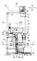
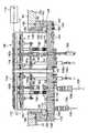
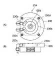
図2は本発明になる基板処理装置の一実施例の構成を示す正面図である。図3は本発明になる基板処理装置の一実施例の構成を示す側面図である。図4は図2中A−A線に沿う横断面図である。
【0031】
図2乃至図4に示されるように、基板処理装置20は、後述するように、シリコン基板の紫外光ラジカル酸化処理と、かかる紫外光ラジカル酸化処理により形成された酸化膜の高周波リモートプラズマを使ったラジカル窒化処理とを、連続して行うことができるように構成されている。
【0032】
基板処理装置20の主要構成は、内部に処理空間が画成された処理容器22と、処理容器22の内部に挿入された被処理基板(シリコン基板)を所定温度に加熱するヒータ部24と、処理容器22の上部に搭載された紫外線照射部26と、窒素ラジカルを供給するリモートプラズマ部27と、被処理基板を回転させる回転駆動部28と、処理空間に挿入された被処理基板を昇降させるリフタ機構30と、処理容器22の内部を減圧するための排気経路32と、処理容器22の内部にガス(窒素ガス、酸素ガス等のプロセスガス)を供給するためのガス供給部34とからなる。
【0033】
また、基板処理装置20は、上記各主要構成部を支持するためのフレーム36を有する。フレーム36は、鉄骨を立体的に組み合わせたものであり、床面に載置される台形状の底部フレーム38と、底部フレーム38の後部より垂直方向に起立された垂直フレーム40,41と、垂直フレーム40の中間部より水平方向に延在するように横架された中間フレーム42と、垂直フレーム40,41の上端部より水平方向に横架された上部フレーム44とから構成されている。
【0034】
底部フレーム38には、冷却水供給部46、電磁弁からなる排気用バルブ48a,48b、ターボ分子ポンプ50、真空管路51、紫外線照射部26の電源ユニット52、リフタ機構30の駆動部136、ガス供給部34などが搭載されている。
【0035】
垂直フレーム40の内部には、各種ケーブルが挿通されるケーブルダクト40aが形成されている。また、垂直フレーム41の内部には、排気ダクト41aが形成されている。さらに、垂直フレーム40の中間部に固定されたブラケット58には、緊急停止スイッチ60が取り付けられ、垂直フレーム41の中間部に固定されたブラケット62には、冷却水による温度調整を行う温度調整器64が取り付けられている。
【0036】
中間フレーム42には、上記処理容器22、紫外線照射部26、リモートプラズマ部27、回転駆動部28、リフタ機構30、UVランプコントローラ57が支持されている。また、上部フレーム44には、ガス供給部34から引き出された複数のガス管路58が連通されたガスボックス66、イオンゲージコントローラ68、圧力制御を行うAPCコントローラ70、ターボ分子ポンプ50を制御するTMPコントローラ72などが搭載されている。
【0037】
図5は処理容器22の下方に配置された機器の構成を示す正面図である。図6は処理容器22の下方に配置された機器の構成を示す平面図である。図7は処理容器22の下方に配置された機器の構成を示す側面図である。図8は排気経路32の構成を示す図であり、(A)は平面図、(B)は正面図、(C)はB−B線に沿う縦断面図である。
【0038】
図5乃至図7に示されるように、処理容器22の後部下方には、処理容器22内部のガスを排気する排気経路32が設けられている。この排気経路32は、横幅寸法が処理容器22の内部に形成された処理空間の横幅と略同一寸法に形成された長方形状の排気口74と連通するように取り付けられている。
【0039】
このように、排気口74が処理容器22内部の横幅寸法に応じた長さに延在形成されているため、処理容器22の前部22a側から内部に供給されたガスは、後述するように処理容器22の内部を通過して後方へ向かう流れとなり、一定流速(層流)のまま排気経路32へ効率良く排気される。
【0040】
図8(A)〜(C)に示されるように、排気経路32は、排気口74に連通される長方形状の開口部32aと、開口部32aの左右側面が下方に向けてテーパ状に傾斜したテーパ部32bと、テーパ部32bの下端で通路面積が絞られた底部32cと、底部32cから前方に突出するL字状の主排気管32dと、主排気管32dの下端に開口する排出口32eと、テーパ部32bの下部32fに開口するバイパス用排出口32gとを有する。排出口32eは、ターボ分子ポンプ50の吸気口に連通される。また、バイパス用排出口32gは、バイパス管路51aに連通される。
【0041】
図5乃至図7に示されるように、処理容器22の排気口74から排出されたガスは、ターボ分子ポンプ50の吸引力により長方形状に形成された開口部32aから流入してテーパ部32bを通過して底部32cに至り、主排気管32d及び排出口32eを介してターボ分子ポンプ50に導かれる。
【0042】
ターボ分子ポンプ50の吐出管50aは、バルブ48aを介して真空管路51に連通されている。そのため、処理容器22の内部に充填されたガスは、バルブ48aが開弁されると、ターボ分子ポンプ50を介して真空管路51へ排出される。また、排気経路32のバイパス用排出口32gには、バイパス管路51aが接続されており、このバイパス管路51aは、バルブ48bの開弁により真空管路51と連通される。
【0043】
ここで、本発明の要部を構成する処理容器22及びその周辺機器の構成について説明する。
【0044】
〔処理容器22の構成〕
図9は処理容器22及びその周辺機器を拡大して示す側面縦断面図である。図10は蓋部材82を外した処理容器22の内部を上方からみた平面図である。
図9及び図10に示されるように、処理容器22は、チャンバ80の上部開口を蓋部材82により閉塞する構成であり、内部がプロセス空間(処理空間)84になっている。
【0045】
処理容器22は、前部22aにガスが供給される供給口22gが形成され、後部22bに搬送口94が形成されている。供給口22gには、後述するガス噴射ノズル部93が設けられ、搬送口94には後述するゲートバルブ96が連通される。
【0046】
図11は処理容器22の平面図である。図12は処理容器22の正面図である。図13は処理容器22の底面図である。図14は図12中C−C線に沿う縦断面図である。図15は処理容器22の右側面図である。図16は処理容器22の左側面図である。
【0047】
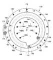
図11乃至図16に示されるように、処理容器22の底部22cには、ヒータ部24が挿入される開口73と、前述した長方形状に開口した排気口74とが設けられている。排気口74には、前述した排気経路32が連通される。尚、チャンバ80及び蓋部材82は、例えば、アルミ合金を切削加工して上記のような形状に加工したものである。
【0048】
また、処理容器22の右側面22eには、プロセス空間84を覗くための第1、第2の窓75,76と、プロセス空間84の温度を測定するためのセンサユニット77が取り付けられている。
【0049】
本実施例では、右側面22eの中央より左側に楕円形に形成された第1の窓75が配置され、右側面22eの中央より右側に円形に形成された第2の窓76が配置されているので、両方向からプロセス空間84に保持された被処理基板Wの状態を直接目視することができるので、被処理基板Wの成膜状況などを観測するのに有利である。
【0050】
尚、窓75,76は、熱電対などの温度測定器具を挿入する場合に処理容器22から外すことが可能な構成になっている。
【0051】
また、処理容器22の左側面22dには、プロセス空間84の圧力を測定するためのセンサユニット85が取り付けられている。このセンサユニット85には、測定レンジの異なる3個の圧力計85a〜85cが設けられており、プロセス空間84の圧力変化を高精度に測定することが可能である。
【0052】
また、プロセス空間84を形成する処理容器22の内壁の四隅には、R形状に形成された湾曲部22hが設けられており、この湾曲部22hにより応力集中を回避すると共に、ガス噴射ノズル部93から噴射されたガス流が安定化するように作用する。
【0053】
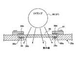
〔紫外線照射部26の構成〕
図8乃至図11に示されるように、紫外線照射部26は、蓋部材82の上面に取り付けられている。この紫外線照射部26の筐体26aの内部には、円筒状に形成された2本の紫外線光源(UVランプ)86,87が所定間隔で平行に配置されている。
【0054】
この紫外線光源86,87は、波長が172nmの紫外線を発光する特性を有しており、蓋部材82に形成された横方向に延在形成された長方形状の開口82a,82bを介してプロセス空間84に保持された被処理基板Wの上面に対向するようにプロセス空間84の前側半分(図8では左半分)の領域に紫外線を照射する位置に設けられている。
【0055】
また、直線状に延在する紫外線光源86,87から被処理基板W上に照射される紫外線の強度分布は、一様ではなく、被処理基板Wの半径方向の位置によって変化しており、一方が被処理基板Wの外周側ほど減少し、他方が内周側ほど減少する。このように紫外線光源86,87は、単独では単調に変化する紫外線強度分布を被処理基板W上に形成するが、被処理基板Wに対する紫外線強度分布の変化方向が逆になっている。
【0056】
そのため、紫外線光源86,87の駆動パワーをUVランプコントローラ57の制御により最適化することにより、被処理基板W上に非常に一様な紫外線強度分布を実現することが可能になる。
【0057】
尚、かかる駆動パワーの最適値は、紫外線光源86,87への駆動出力を変化させて成膜結果を評価することで最適値を求めることができる。
【0058】
また、被処理基板Wと紫外線光源86,87の円筒形状の円筒芯の中心との距離は、例えば、50〜300mmに設定されており、望ましくは100〜200mm程度が良い。
【0059】
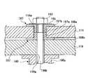
図17は紫外線光源86,87の取付構造を拡大して示す縦断面図である。
図17に示されるように、紫外線光源86,87は、紫外線照射部26の筐体26aの底部開口26bに対向する位置に保持されている。そして、底部開口26bは、プロセス空間84に保持された被処理基板Wの上面に対向する位置に開口すると共に、紫外線光源86,87の全長よりも長い横幅寸法の長方形状に形成されている。
【0060】
底部開口26bの周縁部26cには、透明な石英により形成された透明窓88が取り付けられている。透明窓88は、紫外線光源86,87から照射された紫外線をプロセス空間84に透過する共に、プロセス空間84が減圧されたときの圧力差にも耐える強度を有している。
【0061】
また、透明窓88の下面周縁部には、底部開口26bの周縁部26cの溝内に装着されたシール部材(Oリング)89が当接するシール面88aが形成されている。このシール面88aは、シール部材89を保護するためのコーティングまたは黒石英により形成されている。これにより、シール部材89の材質が分解せず、劣化を防止してシール性能を確保すると共に、シール部材89の材質がプロセス空間84に侵入することを防止する。
【0062】
また、透明窓88の上面周縁部には、ステンレス製のカバー88bが当接しており、透明窓88を締結部材91により挟持する際の強度を高めることで、締結時の押圧力により透明窓88が破損することを防止する。
【0063】
また、本実施例では、紫外線光源86,87及び透明窓88がガス噴射ノズル部93から噴射されたガス流の流れ方向に対して直交する方向に延在するように設けたが、これに限らず、例えば、紫外線光源86,87及び透明窓88をガス流の流れ方向に延在する方向に設けるようにしても良い。
【0064】
〔ガス噴射ノズル部93の構成〕
図9及び図10に示されるように、処理容器22は、前部22aに開口する供給口22gに窒素ガスまたは酸素ガスをプロセス空間84内部に噴射するガス噴射ノズル部93が設けられている。このガス噴射ノズル部93は、後述するようにプロセス空間84の横幅方向に複数の噴射口93aが一列に配置されており、複数の噴射口93aから噴射されたガスが層流状態で被処理基板Wの表面を通過するようにプロセス空間84の内部に安定した流れを発生させる。
【0065】
尚、プロセス空間84を閉塞する蓋部材82の下面と被処理基板Wとの距離は、例えば、5〜100mmに設定されており、望ましくは25〜85mm程度が良い。
【0066】
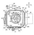
〔ヒータ部24の構成〕
図9及び図10に示されるように、ヒータ部24は、アルミ合金製のベース110と、ベース110上に固定された透明な石英ベルジャ112と、石英ベルジャ112の内部空間113に収納されたSiCヒータ114と、不透明石英により形成された熱反射部材(リフレクタ)116と、石英ベルジャ112の上面に載置されSiCヒータ114により加熱されるSiCサセプタ(加熱部材)118と、を備えた構成である。
【0067】
そのため、SiCヒータ114及び熱反射部材116は、石英ベルジャ112の内部空間113に隔離されており、プロセス空間84でのコンタミネーションが防止される。また、洗浄工程においては、プロセス空間84内に露出されたSiCサセプタ118のみを洗浄すれば良いので、SiCヒータ114及び熱反射部材116を洗浄する手間を省略することが可能になる。
【0068】
被処理基板Wは、保持部材120によりSiCサセプタ118の上方に対向するように保持される。一方、SiCヒータ114は、熱反射部材116の上面に載置されており、SiCヒータ114の発熱は、SiCサセプタ118に放射されると共に、熱反射部材116で反射された熱もSiCサセプタ118に放射される。尚、本実施例のSiCヒータ114は、SiCサセプタ118から僅かに離間した状態で約700°Cの温度に加熱される。
【0069】
SiCサセプタ118は、熱伝導率が良いので、SiCヒータ114からの熱を被処理基板Wに効率良く伝達して被処理基板Wが周縁部分と中心部分との温度差を無くして、被処理基板Wが温度差で反ることを防止する。
【0070】
〔回転駆動部28の構成〕
図9及び図10に示されるように、回転駆動部28は、SiCサセプタ118の上方で被処理基板Wを保持する保持部材120と、上記ベース110の下面に固定されたケーシング122と、ケーシング122により画成された内部空間124内で保持部材120の軸120dに結合されたセラミック軸126を回転駆動させるモータ128と、モータ128の回転を伝達するためのマグネットカップリング130とから構成されている。
【0071】
回転駆動部28においては、保持部材120の軸120dが石英ベルジャ112を貫通してセラミック軸126に結合され、セラミック軸126とモータ128の回転軸との間がマグネットカップリング130を介して非接触で駆動力を伝達する構成であるので、回転駆動系の構成がコンパクトになっており、装置全体の小型化にも寄与している。
【0072】
保持部材120は、軸120dの上端より水平方向に放射状(周方向に120度間隔)に延在する腕部120a〜120cを有する。被処理基板Wは、保持部材120の腕部120a〜120cに載置された状態で保持される。このように保持された被処理基板Wは、保持部材120と共にモータ128により一定の回転速度で回転されており、これによりSiCヒータ114の発熱による温度分布が平均化されると共に、紫外線光源86,87から照射される紫外線の強度分布が均一になり、表面に均一な成膜が施される。
【0073】
〔リフタ機構30の構成〕
図9及び図10に示されるように、リフタ機構30は、チャンバ80の下方、且つ石英ベルジャ112の側方に設けられ、チャンバ80内に挿入された昇降アーム132と、昇降アーム132に連結された昇降軸134と、昇降軸134を昇降させる駆動部136とから構成されている。昇降アーム132は、例えば、セラミックまたは石英により形成されており、図10に示されるように、昇降軸134の上端が結合された結合部132aと、SiCサセプタ118の外周を囲む環状部132bとを有する。そして、昇降アーム132には、環状部132bの内周より中心に延在する3本の当接ピン138a〜138cが周方向に120度間隔で設けられている。
【0074】
当接ピン138a〜138cは、SiCサセプタ118の外周から中心に向かって延在形成された溝118a〜118cに嵌合する位置に降下しており、昇降アーム132が上昇することによりSiCサセプタ118の上方に移動する。また、当接ピン138a〜138cは、SiCサセプタ118の中心より外周側に延在するように形成された保持部材120の腕部120a〜120cと干渉しないように配置されている。
【0075】
昇降アーム132は、搬送ロボット98のロボットハンドが被処理基板Wを取り出す直前に上記当接ピン138a〜138cを被処理基板Wの下面に当接させて被処理基板Wを保持部材120の腕部120a〜120cより持ち上げる。これにより、搬送ロボット98のロボットハンドは、被処理基板Wの下方に移動することが可能になり、昇降アーム132が降下することで被処理基板Wを保持して搬送することが可能になる。
【0076】
〔石英ライナ100の構成〕
図9及び図10に示されるように、処理容器22の内部には、紫外線を遮断するため、例えば白色などの不透明石英により形成された石英ライナ100が装着されている。また、石英ライナ100は、後述するように下部ケース102と、側面ケース104と、上部ケース106と、石英ベルジャ112の外周を覆う円筒状ケース108とを組み合わせた構成になっている。
【0077】
この石英ライナ100は、プロセス空間84を形成する処理容器22及び蓋部材82の内壁を覆うことにより、処理容器22及び蓋部材82の熱膨張を防止する断熱効果が得られると共に、処理容器22及び蓋部材82の内壁が紫外線によって酸化することを防止し、且つ金属のコンタミネーションを防止する役目を有している。
【0078】
〔リモートプラズマ部27の構成〕
図9及び図10に示されるように、プロセス空間84に窒素ラジカルを供給するリモートプラズマ部27は、処理容器22の前部22aに取り付けられており、供給管路90を介して処理容器22の供給口92に連通されている。
【0079】
このリモートプラズマ部27では、Arなどの不活性ガスと共に窒素ガスが供給され、これをプラズマにより活性化することにより、窒素ラジカルを形成することが可能である。このようにして形成された窒素ラジカルは、被処理基板Wの表面に沿って流れ、基板表面を窒化する。
【0080】
また、窒素ガスの他に、O2,NO,N2O,NO2,NH3ガス等を用いた酸化、酸窒化ラジカルプロセスも実施可能である。
【0081】
〔ゲートバルブ96の構成〕
図9及び図10に示されるように、処理容器22の後部には、被処理基板Wを搬送するための搬送口94が設けられている。この搬送口94は、ゲートバルブ96により閉塞されており、被処理基板Wを搬送するときのみゲートバルブ96の開動作により開放される。
【0082】
ゲートバルブ96の後方には、搬送ロボット98が設けられている。そして、ゲートバルブ96の開動作に合わせて搬送ロボット98のロボットハンドが搬送口94よりプロセス空間84内部に進入して被処理基板Wの交換作業を行う。
〔上記各構成部の詳細〕
(1)ここで、上記ガス噴射ノズル部93の構成について詳細に説明する。
図18はガス噴射ノズル部93の構成を拡大して示す縦断面図である。図19はガス噴射ノズル部93の構成を拡大して示す横断面図である。図20はガス噴射ノズル部93の構成を拡大して示す正面図である。
【0083】
図18乃至図20に示されるように、ガス噴射ノズル部93は、前面中央に上記リモートプラズマ部27の供給管路90が連通される連通孔92を有し、連通孔92の上方に複数の噴射孔93a1〜93anが横方向に一列に配設されたノズル板93b1〜93b3が取り付けられている。噴射孔93a1〜93anは、例えば、直径1mmの小孔であり、10mm間隔で設けられている。
【0084】
また、本実施例では、小孔からなる噴射孔93a1〜93anを設けたが、これに限らず、例えば、細いスリットを噴射孔として設ける構成としても良い。
【0085】
また、ノズル板93b1〜93b3は、ガス噴射ノズル部93の壁面に締結されている。そのため、噴射孔93a1〜93anから噴射されたガスは、ガス噴射ノズル部93の壁面より前方に流れる。
【0086】
例えば、噴射孔93a1〜93anがパイプ状のノズル管路に設けられている場合には、噴射孔93a1〜93anから噴射されたガスの一部がノズル管路の後方に回り込むような流れが生じてしまい、プロセス空間84内にガス溜まりが発生して被処理基板W周辺のガス流が安定しないという問題が生じる。
【0087】
しかしながら、本実施例では、噴射孔93a1〜93anがガス噴射ノズル部93の壁面に形成される構成であるので、このようなガスがノズル後方に戻るという現象が発生せず、被処理基板W周辺のガス流を安定した層流状態に保つことが可能になる。これにより、被処理基板W上の成膜が均一に形成される。
【0088】
また、各ノズル板93b1〜93b3に対向する内壁には、ガス溜まりとして機能する凹部93c1〜93c3が形成されている。この凹部93c1〜93c3が噴射孔93a1〜93anの上流に設けられているので、各噴射孔93a1〜93anから噴射されるガスの夫々の流速を平均化にすることができる。これにより、プロセス空間84の全域における流速を平均化することが可能になる。
【0089】
さらに、各凹部93c1〜93c3は、ガス噴射ノズル部93を貫通するガス供給孔93d1〜93d3が連通されている。尚、中央のガス供給孔93d2は、連通孔92と交差しないように横方向にずらした位置に形成されており、クランク形状に曲げられている。
【0090】
そして、中央のガス供給孔93d2には、第1のマスフローコントローラ97aによって流量制御されたガスがガス供給管路992を介して供給される。また、ガス供給孔93d2の左右に配置されたガス供給孔93d1,93d3には、第2のマスフローコントローラ97bによって流量制御されたガスがガス供給管路991,993を介して供給される。
【0091】
また、第1のマスフローコントローラ97a及び第2のマスフローコントローラ97bは、ガス供給管路994,995を介してガス供給部34と接続されており、ガス供給部34から供給されるガスの流量を予め設定された流量に制御する。
【0092】
第1のマスフローコントローラ97a及び第2のマスフローコントローラ97bから供給されたガスは、ガス供給管路991〜993を介してガス供給孔93d1〜93d3に至り、各凹部93c1〜93c3に充填された後、噴射孔93a1〜93anからプロセス空間84に向けて噴射される。
【0093】
プロセス空間84内のガスは、処理容器22の前部22aの横幅方向に延在する各ノズル板93b1〜93b3の噴射孔93a1〜93anからプロセス空間84の全幅に向かって噴射されるため、プロセス空間84の全域で一定流速(層流)で処理容器22の後部22b側へ流れる。
【0094】
さらに、処理容器22の後部22b側には、後部22bの横幅方向に延在する長方形状の排気口74が開口しているため、プロセス空間84内のガスは、後方へ向かう流れとなり、一定流速(層流)のまま排気経路32へ排気される。
【0095】
また、本実施例においては、2系統の流量制御が可能であるので、例えば、第1のマスフローコントローラ97aと第2のマスフローコントローラ97bとで異なる流量制御することも可能である。
【0096】
これにより、プロセス空間84内に供給されるガスの流量(流速)を異なるように設定してプロセス空間84内におけるガスの濃度分布を変化させることも可能である。さらには、第1のマスフローコントローラ97aと第2のマスフローコントローラ97bとで異なる種類のガスを供給することもでき、例えば、第1のマスフローコントローラ97aにより窒素ガスの流量制御を行い、第2のマスフローコントローラ97bにより酸素ガスの流量制御を行うことも可能である。
【0097】
使用ガスとしては、例えば、酸素含有ガス、窒素含有ガス、並びに希ガス等が挙げられる。
【0098】
(2)ここで、ヒータ部24の構成について詳細に説明する。
図21はヒータ部24の構成を拡大して示す縦断面図である。図22はヒータ部24を拡大して示す底面図である。
【0099】
図21及び図22に示されるように、ヒータ部24は、アルミ合金製のベース110に石英ベルジャ112を載置し、処理容器22の底部22cにフランジ140を介して固定される。そして、石英ベルジャ112の内部空間113には、SiCヒータ114及び熱反射部材116が収納される。そのため、SiCヒータ114及び熱反射部材116は、処理容器22のプロセス空間84から隔離されており、プロセス空間84のガスと接触せず、コンタミネーションが生じない構成になっている。
【0100】
SiCサセプタ118は、SiCヒータ114と対向するように石英ベルジャ112上に載置されており、パイロメータ119によって温度が測定される。このパイロメータ119は、SiCサセプタ118が加熱されるのに伴って生じる焦電効果(パイロ電気効果)によりSiCサセプタ118の温度を測定するものであり、制御回路では、パイロメータ119により検出された温度信号から被処理基板Wの温度を推測し、この推測温度に基づいてSiCヒータ114の発熱量を制御する。
【0101】
また、石英ベルジャ112の内部空間113は、後述するように処理容器22のプロセス空間84を減圧するとき、プロセス空間84との圧力差が小さくなるように減圧システムが作動して同時に減圧される。そのため、石英ベルジャ112は、減圧工程時の圧力差を考慮して肉厚(例えば30mm程度)にする必要がなく、熱容量が小さくて済み、その分加熱時の応答性を高められる。
【0102】
ベース110は、円盤状に形成されており、中央に保持部材120の軸120dが挿通される中央孔142を有し、内部には周方向に延在形成された冷却水用の第1の水路144が設けられている。ベース110は、アルミ合金製であるので、熱膨張率が大きいが、第1の水路144に冷却水を流すことにより、冷却される。
【0103】
また、フランジ140は、ベース110と処理容器22の底部22cとの間に介在する第1のフランジ146と、第1のフランジ146の内周に嵌合する第2のフランジ148とを組み合わせた構成である。第1のフランジ146の内周面には、周方向に延在形成された冷却水用の第2の水路150が設けられている。
【0104】
上冷却水供給部46から供給された冷却水は、上記水路144及び150を流れることにより、SiCヒータ114の発熱により加熱されたベース110及びフランジ140を冷却してベース110及びフランジ140の熱膨張を抑える。
【0105】
また、ベース110の下面には、水路144に冷却水を流入させる第1の流入管路152が連通される第1の流入口154と、水路144を通過した冷却水を排出する流出管路156が連通される第1の流出口158とが設けられている。さらに、ベース110の下面の外周近傍には、第1のフランジ146に締結されるボルト160を挿通するための取付孔162が周方向に複数(例えば、8〜12箇所程度)設けられている。
【0106】
また、ベース110下面の半径方向上の中間位置付近には、SiCヒータ114の温度を測定するための熱電対からなる温度センサ164と、SiCヒータ114に電源を供給するための電源ケーブル接続用端子(ソルトン端子)166a〜166fが設けられている。尚、SiCヒータ114には、3つの領域が形成されており、電源ケーブル接続用端子166a〜166fは各領域に電源を供給する+側端子、−側端子として設けられている。
【0107】
また、フランジ140の下面には、水路150に冷却水を流入させる第2の流入管路168が連通される第2の流入口170と、水路150を通過した冷却水を排出する流出管路172が連通される第2の流出口174とが設けられている。
【0108】
図23は第2の流入口170及び第2の流出口174の取付構造を拡大して示す縦断面図である。図24はフランジ140の取付構造を拡大して示す縦断面図である。
【0109】
図23に示されるように、第1のフランジ146には、第2の流入口170が連通されたL字状の連通孔146aが設けられている。この連通孔146aの端部は、水路150に連通されている。また、第2の流出口174も上記第2の流入口170と同様な構成で水路150に連通されている。
【0110】
水路150は、フランジ140の内部に周方向に延在形成されているため、フランジ140を冷却することにより、第1のフランジ146の段部146bとベース110との間で挟持された石英ベルジャ112の鍔部112aの温度も間接的に冷却している。これにより、石英ベルジャ112の鍔部112aが半径方向に熱膨張することを抑制することができる。
【0111】
図23及び図24に示されるように、石英ベルジャ112の鍔部112aの下面には、複数の位置決め孔178が周方向に所定間隔毎に設けられている。この位置決め孔178は、ベース110の上面に螺入されたピン176が嵌合する孔であるが、熱膨張率の大きいベース110が半径方向に熱膨張したときに鍔部112aに負荷がかからないようにピン176の外径よりも大径に形成されている。すなわち、ピン176と位置決め孔178とのクリアランス分だけ石英ベルジャ112の鍔部112aに対するベース110の熱膨張が許容される。
【0112】
また、石英ベルジャ112の鍔部112aは、第1のフランジ146の段部146bに対して半径方向のクリアランスが設けられているので、この点からもこのクリアランス分だけベース110の熱膨張が許容される。
【0113】
石英ベルジャ112の鍔部112aの下面は、ベース110の上面に装着されたシール部材(Oリング)180によってシールされ、石英ベルジャ112の鍔部112aの上面は、第1のフランジ146に装着されたシール部材(Oリング)182によってシールされる。
【0114】
さらに、第1のフランジ146及び第2のフランジ148の上面は、処理容器22の底部22cに装着されたシール部材(Oリング)184,186によってシールされる。また、第2のフランジ148の下面は、ベース110の上面に装着されたシール部材(Oリング)188によってシールされる。
【0115】
このように、ベース110とフランジ140との間、及びフランジ140と処理容器22の底部22cとの間は、夫々2重シール構造になっており、どれか一つのシール部材が破損しても他のシール部材によってシールすることができるので、処理容器22とヒータ部24との間のシール構造に対する信頼性がより高められている。
【0116】
例えば、石英ベルジャ112が割れた場合、あるいは鍔部112aにひび割れが生じた場合、鍔部112aよりも外側に配置されたシール部材180によって石英ベルジャ112内部の気密性が確保され、処理容器22内のガスが外部に流出することが阻止される。
【0117】
あるいは、ヒータ部24に近い方のシール部材180,182が劣化した場合でも、ヒータ部24よりも離れた位置に装着された外側のシール部材186,188によって処理容器22とベース110との間のシール性能が維持されるため、経年変化によるガス漏れも防止できる。
【0118】
図21に示されるように、SiCヒータ114は、石英ベルジャ112の内部空間113において、熱反射部材116の上面に載置されており、且つベース110の上面に起立する複数のクランプ機構190によって所定高さに保持されている。
【0119】
このクランプ機構190は、熱反射部材116の下面に当接する外筒190aと、外筒190aを貫通してSiCヒータ114の上面に当接する軸190bと、軸190bに対して外筒190aを押圧するコイルバネ192とを有する。
【0120】
そして、クランプ機構190は、コイルバネ192のバネ力でSiCヒータ114及び熱反射部材116を挟持する構成になっているため、例えば、運搬時の振動が入力された場合でもSiCヒータ114及び熱反射部材116が石英ベルジャ112に接触しないように保持することが可能になる。また、上記コイルバネ192のバネ力が常に作用することで、熱膨張によるネジのゆるみも防止されており、SiCヒータ114及び熱反射部材116はがたつきの無い安定状態に保持される。
【0121】
また、各クランプ機構190は、ベース110に対してSiCヒータ114及び熱反射部材116の高さ位置を任意の位置に調整できるように構成されており、複数のクランプ機構190の高さ位置調整によってSiCヒータ114及び熱反射部材116の水平に保持することが可能になる。
【0122】
さらに、石英ベルジャ112の内部空間113には、SiCヒータ114の各端子とベース110に挿通された電源ケーブル接続用端子166a〜166fとを電気的に接続するための接続部材194a〜194f(但し、図21には接続部材194a,194cが図示してある)取り付けられている。
【0123】
図25はクランプ機構190の上端部の取付構造を拡大して示す縦断面図である。
図25に示されるように、クランプ機構190は、熱反射部材116の挿通孔116a及びSiCヒータ114の挿通孔114eに挿通された軸190bの上端に螺入されたナット193を締め付けることで、ワッシャ195を介してL字状ワッシャ197,199を軸方向に押圧してSiCヒータ114を挟持する。
【0124】
SiCヒータ114は、挿通孔114eにL字状ワッシャ197,199の円筒部197a、199aが挿入され、円筒部197a,199a内にクランプ機構190の軸190bが挿通される。そして、L字状ワッシャ197,199の鍔部197b,199bがSiCヒータ114の上面,下面に当接する。
【0125】
クランプ機構190の軸190bは、上記コイルバネ192のバネ力により下方に付勢され、且つクランプ機構190の外筒190aは、上記コイルバネ192のバネ力により上方に付勢されている。このように、コイルバネ192のバネ力がクランプ力として作用するため、熱反射部材116及びSiCヒータ114は、安定的に保持され、運搬時の振動による破損が防止される。
【0126】
SiCヒータ114の挿通孔114eは、L字状ワッシャ197a,197bの円筒部197c、197dよりも大径であり、クリアランスが設けられている。そのため、SiCヒータ114の発熱によって生じる熱膨張により挿通孔114eと軸190bとの位置が相対変位した場合、挿通孔114eはL字状ワッシャ197,199の鍔部197b,199bに当接したまま水平方向にずれることが可能になり、熱膨張に伴う応力の発生が防止される。
【0127】
(3)ここで、SiCヒータ114について説明する。
図26に示されるように、SiCヒータ114は、中心部に円形状に形成された第1の発熱部114aと、第1の発熱部114aの外周を囲むように円弧状に形成された第2、第3の発熱部114b,114cとから構成されている。また、SiCヒータ114の中心には、保持部材120の軸120dが挿通される挿通孔114dが設けられている。
【0128】
発熱部114a〜114cは、夫々ヒータ制御回路196に並列に接続されており、温度調整器198によって設定された任意の温度に制御される。ヒータ制御回路196では、電源200から発熱部114a〜114cに供給される電圧を制御することによりSiCヒータ114から放射される発熱量を制御する。
【0129】
また、発熱部114a〜114cによって容量が異なると、電源200の負担が増大するため、本実施例では、各発熱部114a〜114cの容量(2KW)が同一になるように抵抗が設定されている。
【0130】
ヒータ制御回路196は、発熱部114a〜114cを同時に通電して発熱させる制御方法Iと、被処理基板Wの温度分布状況に応じて中心の第1の発熱部114aあるいは外側の第2、第3の発熱部114b,114cの何れか一方を発熱させる制御方法IIと、被処理基板Wの温度変化に応じて発熱部114a〜114cを同時に発熱させたり、第1の発熱部114aあるいは第2、第3の発熱部114b,114cの何れかを発熱させたりする制御方法IIIを選択することができる。
【0131】
被処理基板Wは、上記保持部材120により保持された状態で回転しながら各発熱部114a〜114cの発熱により加熱される際、外周側と中心部分との温度差によって周縁部分が上方に反ることがある。しかしながら、本実施例では、SiCヒータ114は、熱伝導率が良いSiCサセプタ118を介して被処理基板Wを加熱するため、被処理基板Wの全体がSiCヒータ114からの熱で加熱され、被処理基板Wの周縁部分と中心部分との温度差を小さく抑えられて、被処理基板Wが反ることを防止する。
【0132】
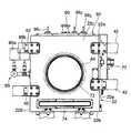
(4)ここで、石英ベルジャ112の構成について詳細に説明する。
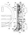
図27は石英ベルジャ112の構成を示す図であり、(A)は平面図、(B)は縦断面図である。図28は石英ベルジャ112の構成を示す図であり、(A)は上方からみた斜視図、(B)は下方からみた斜視図である。
【0133】
図27(a)(b)及び図28(A)(B)に示されるように、石英ベルジャ112は、透明な石英により形成されており、前述した鍔部112aの上方に形成された円筒部112bと、円筒部112bの上方を覆う天板112cと、天板112cの中央より下方に延在する中空部112dと、鍔部112aの内側に形成される開口に横架された補強のための梁部112eとを有する。
【0134】
鍔部112a及び天板112cは、荷重を受けるので、円筒部112bよりも厚く形成されている。また、石英ベルジャ112は、縦方向に延在する中空部112dと横方向に延在する梁部112eとが内部で交差しているため、上下方向及び半径方向の強度が高められている。
【0135】
また、梁部112eの中間位置には、中空部112dの下端部分が結合されており、中空部112d内の挿通孔112fは梁部112eも貫通している。この挿通孔112fには、保持部材120の軸120dが挿通される。
【0136】
そして、石英ベルジャ112の内部空間113には、前述したSiCヒータ114及び熱反射部材116が挿入される。また、SiCヒータ114及び熱反射部材116は、円盤状に形成されているが、円弧状に分割可能な構成であり、梁部112eを避けて内部空間113に挿入された後に組み立てられる。
【0137】
さらに、石英ベルジャ112の天板112cには、SiCサセプタ118を支持するためのボス112g〜112iが3箇所(120度間隔)に突出している。そのため、ボス112g〜112iに支持されたSiCサセプタ118は、天板112cから僅かに浮いた状態に載置される。そのため、処理容器22の内部圧力が変化したり、あるいは温度変化が生じることのよりSiCサセプタ118が下方に変動した場合でも、天板112cに接触することが防止される。
【0138】
また、石英ベルジャ112の内部圧力は、後述するように処理容器22のプロセス空間84の圧力と差が50Torr以下になるように減圧システムによる排気流量の制御を行うため、石英ベルジャ112の肉厚を比較的薄く製作することが可能になる。これにより、天板112cの厚さを6〜10mm程度に薄くすることができるので、石英ベルジャ112の熱容量が小さくなって加熱時の熱伝導効率を高めることにより応答性を向上させることが可能になる。尚、本実施例の石英ベルジャ112は、100Torrの圧力に耐える強度を有するように設計されている。
【0139】
図29は減圧システムの排気系統の構成を示す系統図である。
図29に示されるように、処理容器22のプロセス空間84は、前述したようにバルブ48aの開弁により排気口74に連通された排気経路32を介してターボ分子ポンプ50の吸引力により減圧される。さらに、ターボ分子ポンプ50の排気口に接続された真空管路51の下流は、排気されたガスを吸引するポンプ(MBP)201に連通されている。
【0140】
石英ベルジャ112の内部空間113は、排気管路202を介してバイパス管路51aに接続され、回転駆動部28のケーシング122により画成された内部空間124は、排気管路204を介してバイパス管路51aに接続されている。
【0141】
排気管路202には、内部空間113の圧力を測定する圧力計205と、石英ベルジャ112の内部空間113を減圧する際に開弁されるバルブ206とが設けられている。また、バイパス管路51aには、前述したようにバルブ48bが設けられ、且つバルブ48bをバイパスする分岐管路208が設けられている。この分岐管路208には、減圧工程の初期段階に開弁されるバルブ210と、バルブ48bよりも流量を絞るための可変絞り211とが設けられている。
【0142】
また、ターボ分子ポンプ50の排気側には、開閉用のバルブ212と、排気側の圧力を測定する圧力計214とが設けられている。そして、ターボ軸パージ用のN2ラインがターボ分子ポンプ50に連通されたターボ管路216には、逆止弁218、絞り220、バルブ222が設けられている。
【0143】
尚、上記バルブ206,210、212、222は、電磁弁からなり、制御回路からの制御信号により開弁する。
【0144】
上記のように構成された減圧システムでは、処理容器22、石英ベルジャ112、回転駆動部28の減圧工程を行う場合、一気に減圧するのではなく、段階的に減圧して徐々に真空に近づけるように減圧させる。
【0145】
まず、石英ベルジャ112の排気管路202に設けられたバルブ206を開弁することで石英ベルジャ112の内部空間113とプロセス空間84との間が排気経路32を介して連通状態となり、圧力の均一化が行われる。これにより、減圧工程の開始段階での石英ベルジャ112の内部空間113とプロセス空間84との間の圧力差が小さくなる。
【0146】
次に上記分岐管路208に設けられたバルブ210を開弁させて可変絞り211により絞られた小流量による減圧を行う。その後、バイパス管路51aに設けられたバルブ48bを開弁させて排気流量を段階的に増大させる。
【0147】
また、圧力計205により測定された石英ベルジャ112の圧力と、センサユニット85の圧力計85a〜85cにより測定されたプロセス空間84の圧力とを比較し、両圧力の差が50Torr以下であるとき、バルブ48bを開弁させる。これにより、減圧工程において、石英ベルジャ112にかかる内外の圧力差を緩和して石英ベルジャ112に不要な応力が作用しないように減圧工程を行う。
【0148】
そして、所定時間経過後にバルブ48aを開弁させてターボ分子ポンプ50の吸引力による排気流量を増大させて処理容器22、石英ベルジャ112、回転駆動部28の内部を真空になるまで減圧する。
【0149】
(5)ここで、上記保持部材120の構成について説明する。
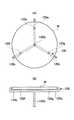
図30は保持部材120の構成を示す図であり、(A)は平面図、(B)は側面図である。
【0150】
図30(A)(B)に示されるように、保持部材120は、被処理基板Wを支持する腕部120a〜120cと、腕部120a〜120cが結合された軸120dとから構成されている。腕部120a〜120cは、プロセス空間84におけるコンタミネーションを防止し、且つSiCサセプタ118からの熱を遮蔽しないようにするため、透明石英により形成されており、軸120dの上端を中心軸として120度間隔で水平方向に放射状に延在している。
【0151】
さらに、腕部120a〜120cの長手方向の中間位置には、被処理基板Wの下面に当接するボス120e〜120gが突出している。そのため、被処理基板Wは、ボス120e〜120gが当接する3点で支持される。
【0152】
このように、保持部材120は、点接触で被処理基板Wを支持する構成であるので、SiCサセプタ118に対して僅かな距離で離間した位置に被処理基板Wを保持することができ。尚、SiCサセプタ118と被処理基板Wとの離間距離は、例えば、1〜20mmであり、望ましくは3〜10mm程度が良い。
【0153】
すなわち、被処理基板Wは、SiCサセプタ118の上方に浮いた状態で回転することになり、直接SiCサセプタ118に載置される場合よりもSiCサセプタ118からの熱が均一に放射され、周縁部分と中心部分の温度差が生じにくく、温度差による被処理基板Wの反りも防止される。
【0154】
被処理基板Wは、SiCサセプタ118から離間した位置に保持されているので、温度差によって反りが生じてもSiCサセプタ118に接触せず、定常時の温度均一化に伴って元の水平状態に復帰することが可能になる。
【0155】
また、保持部材120の軸120dは、不透明石英により棒状に形成されており、上記SiCサセプタ118及び石英ベルジャ112の挿通孔112fに挿通されて下方に延在する。このように、保持部材120は、プロセス空間84内で被処理基板Wを保持するものであるが、石英により形成されているので、金属製のものよりもコンタミネーションのおそれがない。
【0156】
(6)ここで、上記回転駆動部28の構成について詳細に説明する。
図31はヒータ部24の下方に配置された回転駆動部28の構成を示す縦断面図である。図32は回転駆動部28を拡大して示す縦断面図である。
【0157】
図31及び図32に示されるように、ヒータ部24のベース110の下面に回転駆動部28を支持するためのホルダ230が締結されている。このホルダ230には、回転位置検出機構232と、ホルダ冷却機構234とが設けられている。
【0158】
さらに、ホルダ230の下方には、保持部材120の軸120dが挿通固定されたセラミック軸126が挿入されており、セラミック軸126を回転可能に支持するセラミック軸受236,237を保持する固定側のケーシング122がボルト240により固定されている。
【0159】
ケーシング122内においては、回転部分がセラミック軸126とセラミック軸受236,237とから構成されているので、金属のコンタミネーションが防止されている。
【0160】
ケーシング122は、ボルト240が挿通されるフランジ242と、フランジ238より下方に延在形成された有底筒状の隔壁244とを有する。隔壁244の外周面には、前述した減圧システムの排気管路204が連通される排気ポート246が設けられており、ケーシング122の内部空間124の気体は、前述した減圧システムによる減圧工程において、排気されて減圧される。そのため、プロセス空間84内のガスが保持部材120の軸120dに沿って外部に流出することが防止される。
【0161】
さらに、内部空間124には、マグネットカップリング130の従動側マグネット248が収納されている。この従動側マグネット248は、コンタミネーションを防止するため、セラミック軸126の外周に嵌合されたマグネットカバー250に覆われており、内部空間124内の気体と接触しないように取り付けられている。
【0162】
マグネットカバー250は、アルミ合金により環状に形成されたカバーであり、内部に収納する環状の空間が形成されている。内にがたつきの無い状態に収納されている。また、マグネットカバー250の継ぎ目部分は、電子ビーム溶接により隙間無く結合されており、ロウ付け等のように銀が流出してコンタミネーションが生じることがないように加工されている。
【0163】
さらに、ケーシング122の外周には、筒状に形成された大気側回転部252が嵌合するように設けられており、軸受254,255を介して回転可能に支持されている。そして、大気側回転部252の内周には、マグネットカップリング130の駆動側マグネット256が取り付けられている。
【0164】
大気側回転部252は、下端部252aが伝達部材257を介してモータ128の駆動軸128aが結合されている。そのため、モータ128の回転駆動力は、大気側回転部252に設けられた駆動側マグネット256とケーシング122の内部に設けられた従動側マグネット248との間の磁力を介してセラミック軸126に伝達され、保持部材120及び被処理基板Wに伝達される。
【0165】
また、大気側回転部252の外側には、大気側回転部252の回転を検出する回転検出ユニット258が設けられている。この回転検出ユニット258は、大気側回転部252の下端部外周に取り付けられた円盤状のスリット板260,261と、スリット板260,261の回転量を光学的に検出するフォトインタラプタ262,263とから構成されている。
【0166】
フォトインタラプタ262,263は、ブラケット264により固定側のケーシング122に固定されている。そして、回転検出ユニット258では、一対のフォトインタラプタ262,263から回転速度に応じたパルスが同時に検出されるので、両パルスを比較することにより回転検出精度を高めることが可能になる。
【0167】
図33はホルダ冷却機構234の構成を示す図であり、(A)は横断面図、(B)は側面図である。
図33(A)(B)に示されるように、ホルダ冷却機構234は、ホルダ230の内部に周方向に延在する冷却水用の水路230aが形成されている。そして、水路230aの一端に冷却水供給ポート230bが連通され、水路230aの他端に冷却水排出ポート230cが連通されている。
【0168】
冷却水供給部46から供給された冷却水は、冷却水供給ポート230bから水路230aを通過した後、冷却水排出ポート230cから排出されるため、ホルダ230全体を冷却することができる。
【0169】
図34は回転位置検出機構232の構成を示す横断面図である。
図34に示されるように、ホルダ230の一方の側面には、発光素子266が取り付けられ、ホルダ230の他方の側面には、発光素子266からの光を受光する受光素子268が取り付けられている。
【0170】
また、ホルダ230の中央には、保持部材120の軸120dが挿通される中央孔230dが上下方向に貫通しており、この中央孔230dに交差するように横方向に貫通する貫通孔230e,230fが設けられている。
【0171】
発光素子266は、一方の貫通孔230eの端部に挿入され、受光素子268は、他方の貫通孔230fの端部に挿入されている。貫通孔230eと230fとの間には、軸120dが挿通されているため、軸120dの回転位置を受光素子268の出力変化から検出することが可能になる。
【0172】
(7)ここで、回転位置検出機構232の構成及び作用について詳細に説明する。
図35は回転位置検出機構232の構成及び作用を説明するための図であり、(A)は非検出状態を示す図、(B)は検出状態を示す図である。
【0173】
図35(A)に示されるように、保持部材120の軸120dは、外周に接線方向の面取り加工が施されている。この面取り部120iは、発光素子266と受光素子268との中間位置に回動したとき、発光素子266から発光された光と平行になる。
【0174】
このとき、発光素子266からの光は、面取り部120iの横を通過して受光素子268に照射される。これにより、受光素子268の出力信号Sはオンになり、回転位置判定回路270に供給される。
【0175】
図35(B)に示されるように、保持部材120の軸120dが回動して面取り部120iの位置が中間位置からずれると、発光素子266からの光は、軸120dに遮断され、回転位置判定回路270への出力信号Sはオフになる。
【0176】
図36回転位置検出機構232の信号波形図であり、(A)は受光素子268の出力信号Sの波形図、(B)は回転位置判定回路270から出力されるパルス信号Pの波形図である。
【0177】
図36(A)に示されるように、受光素子268は、軸120dの回動位置によって発光素子266からの光の受光量(出力信号S)が放物線状に変化する。回転位置判定回路270では、この出力信号Sに対する閾値Hを設定することで、出力信号Sが閾値H以上になったときにパルスPを出力する。
【0178】
このパルスPが保持部材120の回動位置を検出した検出信号として出力される。すなわち、回転位置判定回路270は、図10に示されるように、保持部材120の腕部120a〜120cが昇降アーム132の当接ピン138a〜138cに干渉せず、且つ搬送ロボット98のロボットハンドと干渉しない位置にあることを判定し、その検出信号(パルスP)を出力する。
【0179】
(8)ここで、上記回転位置判定回路270から出力された検出信号(パルスP)に基づいて制御回路が実行する回転位置制御処理について説明する。
図37は制御回路が実行する回転位置制御処理を説明するためのフローチャートである。
【0180】
図37に示されるように、制御回路は、S11において、被処理基板Wの回転を指示する制御信号があると、S12に進み、モータ128を起動させる。続いて、S13に進み、受光素子268の信号がオンかどうかをチェックする。S13で受光素子268の信号がオンであるときは、S14に進み、検出信号(パルスP)の周期から保持部材120及び被処理基板Wの回転数を演算する。
【0181】
続いて、S15に進み、保持部材120及び被処理基板Wの回転数nが予め設定された目標回転naかどうかをチェックする。S15において、保持部材120及び被処理基板Wの回転数nが目標回転naに達していないときは、上記S13に戻り、モータ128の回転数が上昇したかどうかを再度チェックする。
【0182】
また、上記S15において、n=naのときは、保持部材120及び被処理基板Wの回転数nが目標回転naに達しているので、S17に進み、モータ停止の制御信号があるかどうかをチェックする。S17において、モータ停止の制御信号が無いときは、上記S13に戻り、モータ停止の制御信号があるときは、S18に進み、モータ128を停止させる。続いて、S19で受光素子268の信号がオンかどうかをチェックし、受光素子268の信号がオンになるまで繰り返す。
【0183】
このようにして、保持部材120の腕部120a〜120cが昇降アーム132の当接ピン138a〜138cに干渉せず、且つ搬送ロボット98のロボットハンドと干渉しない位置に停止させることができる。
【0184】
尚、上記回転位置制御処理では、受光素子268からの出力信号の周期から回転数を求める方法を用いた場合について説明したが、例えば前述したフォトインタラプタ262,263から出力された信号を積算して回転数を求めることも可能である。
【0185】
(9)ここで、処理容器122の側面に形成された窓75,76の構成について詳細に説明する。
図38は窓75,76の取付箇所を上方からみた横断面図である。図39は窓75を拡大して示す横断面図である。図40は窓76を拡大して示す横断面図である。
【0186】
図38及び図39に示されるように、第1の窓75は、処理容器122の内部に形成されたプロセス空間84にガスが供給されたり、真空に減圧されるため、気密性がより高められた構成になっている。
【0187】
窓75は、透明石英272と、紫外線を遮断するUVガラス274とを有する2重構造になっている。透明石英272は、窓取り付け部276に当接させた状態で第1の窓枠278が窓取り付け部276にビス277でネジ止めされて固定される。窓取り付け部276の外面には、透明石英272との間を気密にシールするシール部材(Oリング)280が装着されている。さらに、第1の窓枠278の外面には、UVガラス274を当接させた状態で第2の窓枠282がビス284でネジ止めされて固定される。
【0188】
このように、窓75は、紫外線光源(UVランプ)86,87から照射された紫外線がUVガラス274によって遮断されてプロセス空間84の外部に漏れることを防止していると共に、シール部材280のシール効果によってプロセス空間84に供給されたガスが外部に流出することを防止している。
【0189】
また、処理容器22の側面を貫通する開口286は、処理容器22の中央、すなわち保持部材120に保持された被処理基板Wの中心に向かうように斜めに貫通している。そのため、窓75は、処理容器22の側面中心から外れた位置に設けられているが、横方向に広く見えるように楕円形状に形成されており、被処理基板Wの状態を外部から視認することができる。
【0190】
また、第2の窓76は、上記窓75と同様な構成になっており、透明石英292と、紫外線を遮断するUVガラス294とを有する2重構造になっている。透明石英292は、窓取り付け部296に当接させた状態で第1の窓枠298が窓取り付け部296にビス297でネジ止めされて固定される。窓取り付け部296の外面には、透明石英292との間を気密にシールするシール部材(Oリング)300が装着されている。さらに、第1の窓枠298の外面には、UVガラス294を当接させた状態で第2の窓枠302がビス304でネジ止めされて固定される。
【0191】
このように、窓76は、紫外線光源(UVランプ)86,87から照射された紫外線がUVガラス294によって遮断されてプロセス空間84の外部に漏れることを防止していると共に、シール部材300のシール効果によってプロセス空間84に供給されたガスが外部に流出することを防止している。
【0192】
尚、本実施例では、処理容器22の側面に一対の窓75,76を配置した構成を一例として説明したが、これに限らず、3個以上の窓を設けるようにしても良いし、あるいは側面以外の場所に設けるようにしても良いのは勿論である。
【0193】
(10)ここで、石英ライナ100を構成する各ケース102,104,106,108について説明する。
図9及び図10に示されるように、石英ライナ100は、下部ケース102、側面ケース104、上部ケース106、円筒状ケース108とを組み合わせた構成になっており、夫々が不透明石英により形成されており、アルミ合金製の処理容器22をガスや紫外線から保護すると共に、処理容器22による金属のコンタミネーションを防止することを目的として設けられている。
【0194】
図41(A)(B)は下部ケース102の構成を示す図であり、(A)は平面図、(B)は側面図である。
図41(A)(B)に示されるように、下部ケース102は、輪郭形状が処理容器22の内壁形状に対応した板状に形成されており、その中央にはSiCサセプタ118及び被処理基板Wに対向する円形開口310が形成されている。この円形開口310は、円筒状ケース108が挿入可能な寸法に形成されており、内周には保持部材120の腕部120a〜120cの先端部を挿入するための凹部310a〜310cが120度間隔で設けられている。
【0195】
尚、凹部310a〜310cの位置は、保持部材120の腕部120a〜120cが昇降アーム132の当接ピン138a〜138cに干渉せず、且つ搬送ロボット98のロボットハンドと干渉しない位置である。
【0196】
また、下部ケース102には、処理容器22の底部に形成された排気口74に対向する長方形状の開口312が設けられている。さらに、下部ケース102は、下面に位置決め用の突起314a,314bが非対称位置に設けられている。
【0197】
また、上記円形開口310の内周には、後述する円筒状ケース108の突起が嵌合するための凹部310dが形成されている。さらに、下部ケース102の周縁部には、側面ケース104に嵌合する段部315が設けられている。
【0198】
図42は側面ケース104の構成を示す図であり、(A)は平面図、(B)は正面図、(C)は背面図、(D)は左側面図、(E)は右側面図である。
図42(A)〜(E)に示されるように、側面ケース104は、外形状が処理容器22の内壁形状に対応した四隅がR形状とされた略四角形の枠形状に形成されており、内側にプロセス空間84が形成される。
【0199】
また、側面ケース104は、正面104aに前述したガス噴射ノズル部93の複数の噴射口93aに対向するように横方向に延在された細長形状のスリット316と、リモートプラズマ部27に連通される連通孔92に対向する位置に設けられたU字状の開口317とが設けられている。尚、本実施例では、スリット316と開口317とが連通した構成になっているが、夫々独立した開口として形成することも可能である。
【0200】
また、側面ケース104は、背面104bに前述した搬送ロボット98のロボットハンドが通過するための凹部318が搬送口94に対向する位置に形成されている。
【0201】
また、側面ケース104は、左側面104cに前述したセンサユニット85に対向する円形の孔319が形成され、右側面104dに前述した窓75,76と、センサユニット77に対向する孔320〜322が形成されている。
【0202】
図43は上部ケース106の構成を示す図であり、(A)は底面図、(B)は側面図である。
図43(A)(B)に示されるように、上部ケース106は、輪郭形状が処理容器22の内壁形状に対応した板状に形成されており、紫外線光源(UVランプ)86,87に対向する位置に長方形状の開口324,325が形成されている。さらに、上部ケース106の周縁部には、側面ケース104に嵌合する段部326が設けられている。
【0203】
また、上部ケース106は、蓋部材82の形状に対応する円形孔327〜329、及び長方形の四角孔330が設けられている。
【0204】
図44は円筒状ケース108の構成を示す図であり、(A)は平面図、(B)は側面縦断面図、(C)は側面図である。
図44(A)〜(C)に示されるように、円筒状ケース108は、石英ベルジャ112の外周を覆うように筒状に形成されており、上端縁部には昇降アーム132の当接ピン138a〜138cが挿入される凹部108a〜108cが設けられている。さらに、円筒状ケース108は、上端部の外周に下部ケース102の凹部310dが嵌合する位置合わせ用の突起108dが形成されている。
【0205】
(11)ここで、リフタ機構30のシール構造について説明する。
図45はリフタ機構30を拡大して示す縦断面図である。図46はリフタ機構30のシール構造拡大して示す縦断面図である。
【0206】
図45及び図46に示されるように、リフタ機構30は、駆動部136により昇降軸134を昇降させてチャンバ80内に挿入された昇降アーム132を昇降させる際、チャンバ80の貫通孔80a内に挿入された昇降軸134の外周が蛇腹形状のベローズ332により覆われており、チャンバ80内でのコンタミネーションを防止するように構成されている。
【0207】
ベローズ332は、蛇腹部分が伸縮可能な形状になっており、例えばインコネルやハステロイなどにより形成されている。また、貫通孔80aは、昇降軸134が挿通された蓋部材340により閉塞されている。
【0208】
さらに、昇降軸134の上端がボルト334により締結される昇降アーム132の連結部材336には、円筒形状のセラミックカバー338が嵌合固定されている。このセラミックカバー338は、連結部材336より下方に延在形成されるため、ベローズ332の周囲を覆うことによりチャンバ80内で直接露出されないように設けられている。
【0209】
そのため、ベローズ332は、プロセス空間84において、昇降アーム132を上昇させる際に上方に伸びてしまい、セラミックにより形成された円筒状カバー338により覆われている。よって、ベローズ332は、貫通孔80aに昇降可能に挿入された円筒状カバー338によりプロセス空間84のガスや熱に直接晒されることがなく、ガスや熱による劣化を防止されている。
【0210】
(12)以下に、基板処理装置20を使って行う被処理基板W表面の紫外光ラジカル酸化処理、およびその後に行われるリモートプラズマラジカル窒化処理について説明する。
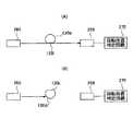
〔紫外光ラジカル酸化処理〕
図47(A)は、それぞれ図2の基板処理装置20を使って被処理基板Wのラジカル酸化を行う場合を示す側面図および平面図、図47(B)は図47(A)の構成を示す平面図である。
図47(A)に示されるように、前記プロセス空間84中にはガス噴射ノズル部93から酸素ガスが供給され、被処理基板Wの表面に沿って流れた後、排気口74、ターボ分子ポンプ50およびポンプ201を通って排気される。ターボ分子ポンプ50を使うことにより、前記プロセス空間84のプロセス圧が、基板Wの酸素ラジカルによる酸化に必要な10-3〜10-6Torrの範囲に設定される。
【0211】
これと同時に、好ましくは172nmの波長の紫外光を発生する紫外線光源86,87を駆動することにより、このようにして形成された酸素ガス流中に酸素ラジカルが形成される。形成された酸素ラジカルは前記被処理基板Wの表面に沿って流れる際に、回動している基板表面を酸化する。このような被処理基板Wの酸素ラジカルによる酸化により、シリコン基板表面に1nm以下の膜厚の非常に薄い酸化膜、特に2〜3原子層に相当する約0.4nmの膜厚の酸化膜を、安定に再現性良く形成することが可能になる。
【0212】
図47(B)に示されるように、紫外線光源86,87は酸素ガス流の方向に交差する方向に延在する管状の光源であり、ターボ分子ポンプ50が排気口74を介してプロセス空間84を排気するのがわかる。一方、前記排気口74から直接にポンプ50に至る、図47(B)中に点線で示した排気経路は、バルブ48bを閉鎖することにより遮断されている。
【0213】
図48は、図2の基板処理装置20において図47(A),(B)の工程によりシリコン基板表面にシリコン酸化膜を、基板温度を450℃に設定し、紫外光照射強度および酸素ガス流量あるいは酸素分圧を様々に変化させながら形成した場合の、膜厚と酸化時間との関係を示す。ただし図48の実験ではラジカル酸化に先立ってシリコン基板表面の自然酸化膜を除去し、また場合によっては基板表面に残留する炭素を紫外光励起窒素ラジカル中において除去し、さらにAr雰囲気中、約950℃における高温熱処理を行うことにより、基板表面を平坦化している。また前記紫外線光源86,87としては、波長が172nmのエキシマランプを使った。
【0214】
図48を参照するに、系列1のデータは、紫外光照射強度を紫外光源24Bの窓面における基準強度(50mW/cm2)の5%に設定し、プロセス圧を665mPa(5mTorr),酸素ガス流量を30SCCMに設定した場合の酸化時間と酸化膜厚との関係を、系列2のデータは紫外光強度をゼロに設定し、プロセス圧を133Pa(1Torr),酸素ガス流量を3SLMに設定した場合の酸化時間と酸化膜厚との関係を示す。また系列3のデータは紫外光強度をゼロに設定し、プロセス圧を2.66Pa(20mTorr),酸素ガス流量を150SCCMに設定した場合の酸化時間と酸化膜厚との関係を示し、系列4のデータは紫外光照射強度を100%、すなわち前記基準強度に設定し、プロセス圧を2.66Pa(20mTorr),酸素ガス流量を150SCCMに設定した場合の酸化時間と酸化膜厚との関係を示す。さらに系列5のデータは紫外光照射強度を基準強度の20%に設定し、プロセス圧を2.66Pa(20mTorr),酸素ガス流量を150SCCMに設定した場合の酸化時間と酸化膜圧との関係を示し、系列6のデータは、紫外光照射強度を基準照射強度の20%に設定し、プロセス圧を約67Pa(0.5Torr)、酸素ガス流量を0.5SLMに設定した場合の酸化時間と酸化膜厚との関係を示す。さらに系列7のデータは、紫外光照射強度を基準強度の20%に設定し、プロセス圧を665Pa(5Torr)に、酸素ガス流量を2SLMに設定した場合の酸化時間と酸化膜厚との関係を、系列8のデータは、紫外光照射強度を基準強度の5%に設定し、プロセス圧を2.66Pa(20mTorr),酸素ガス流量を150SCCMに設定した場合の酸化時間と酸化膜厚との関係を示す。
【0215】
図48の実験において、酸化膜の膜厚はXPS法により求めているが、このように1nmを下回る非常に薄い酸化膜の膜厚を求める統一された方法は、現時点では存在しない。
【0216】
そこで本発明の発明者は、図49に示す観測されたSi2p軌道のXPSスペクトルに対してバックグラウンド補正および3/2と1/2スピン状態の分離補正を行い、その結果得られた図50に示すSi2p3/2XPSスペクトルをもとに、Lu他(Z. H. Lu, et al., Appl. Phys, Lett. 71 (1997), pp.2764)の教示に従って、式(1)に示す式および係数を使って酸化膜の膜厚dを求めた。
d=λsinα・ln[IX+/(βI0+)+1] (1)
λ=2.96
β=0.75
ただし式(1)においてαは図55に示すXPSスペクトルの検出角であり、図示の例では30°に設定されている。また数1中、IX+は酸化膜に対応するスペクトルピークの積分強度(I1x+I2x+I3x+I4x)であり、図50中、102〜104eVのエネルギ領域において見られるピークに対応している。一方、I0+は100eV近傍のエネルギ領域に対応した、シリコン基板に起因するスペクトルピークの積分強度に対応する。
【0217】
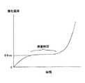
再び図48を参照するに、紫外光照射パワー、従って形成される酸素ラジカル密度が小さい場合(系列1,2,3,8)には、最初は酸化膜の酸化膜厚が0nmであったものが、酸化時間と共に酸化膜厚が徐々に増加し続けるのに対し、紫外光照射パワーを基準強度の20%以上に設定した系列4,5,6,7では、図51に概略的に示すように酸化膜成長が成長開始後、おおよそ0.4nmの膜厚に到達した時点で停留し、ある程度の停留時間が経過した後、急激に成長が再開されるのが認められる。
【0218】
図48あるいは図51の関係は、シリコン基板表面の酸化処理において、0.4nm前後の膜厚の非常に薄い酸化膜を、安定して形成できることを意味している。また、図48に見られるように、かかる停留時間がある程度継続することから、形成される酸化膜は、一様な厚さを有することがわかる。すなわち、本発明によれば、約0.4nmの厚さの酸化膜をシリコン基板上に、一様な厚さに形成することが可能になる。
【0219】
図52(A),(B)は、かかるシリコン基板上への薄い酸化膜の形成過程を概略的に示す。これらの図では、シリコン(100)基板上の構造を極めて単純化していることに注意すべきである。
【0220】
図52(A)を参照するに、シリコン基板表面には、シリコン原子1個あたり2個の酸素原子が結合し、1原子層の酸素層が形成されている。この代表的な状態では、基板表面のシリコン原子は基板内部の2つのシリコン原子と基板表面の二つの酸素原子により配位され、サブオキサイドを形成している。
【0221】
これに対し、図52(B)の状態ではシリコン基板最上部のシリコン原子は4つの酸素原子により配位されており、安定なSi4+の状態をとる。これが理由で、図52(A)の状態では速やかに酸化が進み、図52(B)の状態になって酸化が停留するものと考えられる。図52(B)の状態における酸化膜の厚さは約0.4nmであり、これは図48において観測される停留状態における酸化膜厚と良く一致する。
【0222】
図50のXPSスペクトルにおいて、酸化膜厚が0.1nmあるいは0.2nmの場合に101〜104eVのエネルギ範囲において見られる低いピークが図52(A)のサブオキサイドに対応し、酸化膜厚が0.3nmを超えた場合にこのエネルギ領域に表れるピークがSi4+に起因するもので、1原子層を超える酸化膜の形成を表しているものと考えられる。
【0223】
このような0.4nmの膜厚における酸化膜厚の停留現象は、図47(A),(B)のUVO2ラジカル酸化プロセスに限定されるものではなく、同様に薄い酸化膜が精度よく形成できる酸化膜形成方法であれば、同じように見られるものであると考えられる。
【0224】
図52(B)の状態からさらに酸化を継続すると、酸化膜の厚さは再び増大する。
【0225】
図53は、このように基板処理装置20を使った図47(A),(B)の紫外光ラジカル酸化プロセスにより形成された酸化膜上に厚さが0.4nmのZrSiOx膜と電極膜とを形成し(後で説明する図54(B)を参照)、得られた積層構造に対して求めた熱酸化膜換算膜厚Teqとリーク電流Igとの関係を示す。ただし、図53のリーク電流特性は、前記電極膜とシリコン基板との間にフラットバンド電圧Vfbを基準に、Vfb−0.8Vの電圧を印加した状態で測定している。比較のため、図53中には熱酸化膜のリーク電流特性をも示してある。また図示している換算膜厚は、酸化膜とZrSiOx膜を合わせた構造についてのものである。
【0226】
図53を参照するに、酸化膜を省略した場合、すなわち酸化膜の膜厚が0nmの場合にはリーク電流密度が熱酸化膜のリーク電流密度を超えており、また熱酸化膜換算膜厚Teqも約1.7nm程度の比較的大きな値になることがわかる。
【0227】
これに対し、酸化膜の膜厚を0nmから0.4nmまで増大させると、熱酸化膜換算膜厚Teqの値が減少をはじめるのがわかる。このような状態では酸化膜がシリコン基板とZrSiOx膜との間に介在することになり、物理膜厚は実際には増大するはずなのに換算膜厚Teqは減少しているが、これはシリコン基板上にZrO2膜を直接に形成した場合、図54(A)に示すようにZrのシリコン基板中への拡散あるいはSiのZrSiOx膜中への拡散が大規模に生じ、シリコン基板とZrSiOx膜との間に厚い界面層が形成されていることを示唆している。これに対し、図54(B)に示すように厚さが0.4nmの酸化膜を介在させることにより、このような界面層の形成が抑制され、結果として換算膜厚が減少するものと考えられる。これに伴って、リーク電流の値も酸化膜の厚さと共に減少するのがわかる。ただし図54(A),(B)は、このようにして形成された試料の概略的な断面を示しており、シリコン基板441上に酸化膜442が形成され、酸化膜442上にZrSiOx膜443が形成されている構造を示している。
【0228】
一方、前記酸化膜の膜厚が0.4nmを超えると、熱酸化膜換算膜厚の値は再び増大をはじめる。酸化膜の膜厚が0.4nmを超えた範囲においては、膜厚の増大と共にリーク電流の値も減少しており、換算膜厚の増大は酸化膜の物理膜厚の増大に起因するものであると考えられる。
【0229】
このように、図48で観測された酸化膜の成長が停留する0.4nm付近の膜厚は、酸化膜と高誘電体膜とよりなる系の換算膜厚の最小値に対応しており、図52(B)に示す安定な酸化膜により、Zr等の金属元素のシリコン基板中への拡散が効果的に阻止されること、またこれ以上酸化膜の厚さを増大させても、金属元素の拡散阻止効果はそれほど高まらないことがわかる。
【0230】
さらに0.4nmの厚さの酸化膜を使った場合のリーク電流の値は、対応する厚さの熱酸化膜のリーク電流の値よりも二桁ほど小さく、このような構造の絶縁膜をMOSトランジスタのゲート絶縁膜に使うことにより、ゲートリーク電流を最小化できることがわかる。
【0231】
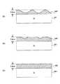
また、図48あるいは図51で説明した酸化膜成長の0.4nmにおける停留現象の結果、図55(A)に示すようにシリコン基板441上に形成された酸化膜442に当初膜厚の変化ないし凹凸が存在していても、酸化膜成長の際に膜厚の増大が図55(B)に示すように0.4nmの近傍において停留するため、停留期間内で酸化膜成長を継続することにより、図55(C)に示す非常に平坦な、一様な膜厚の酸化膜442を得ることができる。
【0232】
先にも説明したように、非常に薄い酸化膜に対しては、現状では統一された膜厚測定方法が存在しない。このため、図55(C)の酸化膜442の膜厚値自体は、測定方法で異なる可能性がある。しかし、先に説明した理由から、酸化膜成長に停留が生じる厚さは、2原子層分の厚さであることがわかっており、従って、好ましい酸化膜442の膜厚は、約2原子層分の厚さであると考えられる。この好ましい厚さには、2原子層分の厚さが酸化膜442全体にわたり確保されるように、部分的に3原子層分の厚さの領域が形成されている場合も含まれる。すなわち、好ましい酸化膜442の厚さは、実際には2〜3原子層の範囲であると考えられる。
〔リモートプラズマラジカル窒化処理〕
図56は、基板処理装置20において使われるリモートプラズマ部27の構成を示す。
図56に示されるように、リモートプラズマ部27は、内部にガス循環通路27aとこれに連通したガス入り口27bおよびガス出口76cを形成された、典型的にはアルミニウムよりなるブロック27Aを含み、前記ブロック27Aの一部にはフェライトコア27Bが形成されている。
【0233】
前記ガス循環通路27aおよびガス入り口27b、ガス出口27cの内面にはフッ素樹脂コーティング27dが施され、前記フェライトコア27Bに巻回されたコイルに周波数が400kHzの高周波を供給することにより、前記ガス循環通路27a内にプラズマ27Cが形成される。
【0234】
プラズマ27Cの励起に伴って、前記ガス循環通路27a中には窒素ラジカルおよび窒素イオンが形成されるが、窒素イオンは前記循環通路27aを循環する際に消滅し、前記ガス出口27cからは主に窒素ラジカルN2*が放出される。さらに図56の構成では前記ガス出口27cに接地されたイオンフィルタ27eを設けることにより、窒素イオンをはじめとする荷電粒子が除去され、前記プロセス空間84には窒素ラジカルのみが供給される。また、前記イオンフィルタ27eを接地させない場合においても、前記イオンフィルタ27eの構造は拡散板として作用し、十分に窒素イオンをはじめとする荷電粒子を除去することが可能になる。
【0235】
図57は、リモートプラズマ部27により形成されるイオンの数と電子エネルギの関係を、マイクロ波プラズマ源の場合と比較して示す。
図57に示されるように、マイクロ波によりプラズマを励起した場合には窒素分子のイオン化が促進され、多量の窒素イオンが形成されることになる。これに対し500kHz以下の高周波によりプラズマを励起した場合には、形成される窒素イオンの数が大幅に減少する。マイクロ波によりプラズマ処理を行う場合には、図58に示すように1.33×10⁻³〜1.33×10⁻⁶Pa(10-1〜10-4Torr)の高真空が必要になるが、高周波プラズマ処理は、13.3〜13.3kPa(0.1〜100Torr)の比較的高い圧力で実行可能である。
【0236】
以下の表1は、マイクロ波によりプラズマを励起する場合と、高周波によりプラズマを励起する場合との間での、イオン化エネルギ変換効率、放電可能圧力範囲、プラズマ消費電力、プロセスガス流量の比較を示す。
【0237】
【表1】
【0238】
基板処理装置20では、酸化膜の窒化処理を窒素イオンではなく窒素ラジカルN2*で行っており、このため励起される窒素イオンの数は少ない方が好ましい。また被処理基板に加えられるダメージを最小化する観点からも、励起される窒素イオンの数は少ないのが好ましい。さらに基板処理装置20では、励起される窒素ラジカルの数も少なく、高誘電体ゲート絶縁膜下の非常に薄い、せいぜい2〜3原子層程度の厚さしかないベース酸化膜を窒化するのに好適である。
【0239】
図59(A),(B)は、それぞれ基板処理装置20を使って被処理基板Wのラジカル窒化を行う場合を示す側面図および平面図である。
図59(A),(B)に示されるように、リモートプラズマ部27にはArガスと窒素ガスが供給され、プラズマを数100kHzの周波数で高周波励起することにより窒素ラジカルが形成される。形成された窒素ラジカルは前記被処理基板Wの表面に沿って流れ、前記排気口74およびポンプ201を介して排気される。その結果前記プロセス空間84は、基板Wのラジカル窒化に適当な、1.33Pa〜13.3kPa(0.01〜100Torr)の範囲のプロセス圧に設定される。このようにして形成された窒素ラジカルは、前記被処理基板Wの表面に沿って流れる際に、被処理基板Wの表面を窒化する。
【0240】
図59(A),(B)の窒化工程では、窒化工程に先立つパージ工程では前記バルブ48aおよび212が開放され、バルブ48aが閉鎖されることで前記プロセス空間84の圧力が1.33×10⁻¹〜1.33×10⁻⁴Paの圧力まで減圧され、プロセス空間84中に残留している酸素や水分がパージされるが、その後の窒化処理ではバルブ48aおよび212は閉鎖され、ターボ分子ポンプ50はプロセス空間84の排気経路には含まれない。
【0241】
このように、基板処理装置20を使うことにより、被処理基板Wの表面に非常に薄い酸化膜を形成し、その酸化膜表面をさらに窒化することが可能になる。
【0242】
図60(A)は、基板処理装置20によりSi基板上に熱酸化処理により2.0nmの厚さに形成された酸化膜を、リモートプラズマ部27を使って、表2に示す条件で窒化した場合の前記酸化膜中における窒素濃度分布を示し、図60(B)は、同じ酸化膜中における窒素濃度分布と酸素濃度分布との関係を示す。
【0243】
【表2】
【0244】
これに対し、マイクロ波プラズマを使った窒化処理では、窒化処理の際の処理圧力がパージ圧と同程度であり、従ってプラズマ雰囲気中において残留酸素は高い熱力学的な活動度を有するものと考えられる。
【0245】
図60(A)を参照するに、マイクロ波励起プラズマにより窒化した場合には酸化膜中に導入される窒素の濃度は限られており、酸化膜の窒化は実質的に進行していないことがわかる。これに対し本実施例のようにRF励起プラズマにより窒化した場合には、酸化膜中において窒素濃度が深さと共に直線的に変化し、表面近傍では20%近い濃度に達していることがわかる。
【0246】
図61は、XPS(X線分光スペクトル)を使って行う図60(A)の測定の原理を示す。
図61を参照するに、シリコン基板411上に酸化膜412を形成された試料には所定の角度で斜めにX線が照射され、励起されたX線スペクトルを検出器DET1,DET2により、様々な角度で検出する。その際、例えば90°の深い検出角に設定された検出器DET1では励起X線の酸化膜412内における行路が短く、従って前記検出器DET1で検出されるX線スペクトルには酸化膜412の下部の情報を多く含まれるに対し、浅い検出角に設定された検出器DET2では、励起X線の酸化膜12中における行路が長く、従って、検出器DET2は主に酸化膜412の表面近傍の情報を検出する。
【0247】
図60(B)は、前記酸化膜中における窒素濃度と酸素濃度との関係を示す。ただし図60(B)中、酸素濃度はO1s軌道に対応するX線強度により表されている。
【0248】
図60(B)を参照するに、酸化膜の窒化を本発明のようにRFリモートプラズマで行った場合には、窒素濃度の増大に伴って酸素濃度が減少しており、酸化膜中において窒素原子が酸素原子を置き換えていることがわかる。これに対し、酸化膜の窒化をマイクロ波プラズマで行った場合には、このような置換関係は見られず、窒素濃度と共に酸素濃度が低下する関係は見られない。また特に図60(B)においては、マイクロ波窒化により5〜6%の窒素を導入した例においては酸素濃度の増加が見られており、これは窒化と共に酸化膜の増膜が起こることを示唆している。このようなマイクロ波窒化に伴う酸素濃度の増加は、マイクロ波窒化が高真空中において行われ、従って処理空間中に残留する酸素あるいは水分が高周波リモートプラズマ窒化の場合のようにArガスや窒素ガスにより希釈されることがなく、雰囲気中において高い活動度を有することによるものと考えられる。
【0249】
図62は、基板処理装置20において酸化膜を4Å(0.4nm)および7Å(0.7nm)の厚さに形成し、これを前記リモートプラズマ部27を使った図59(A),(B)の窒化工程により窒化した場合の窒化時間と膜中の窒素濃度との関係を示す。また図63は、図62の窒化処理に伴う窒素の酸化膜膜表面への偏析の様子を示す。なお、図62及び図63には、酸化膜を急速熱酸化処理により5Å(0.5nm)および7Å(0.7nm)の厚さに形成した場合をも示している。
【0250】
図62を参照するに、膜中の窒素濃度は、いずれの酸化膜であっても窒化処理時間と共に上昇するが、特に紫外光ラジカル酸化により形成された2原子層分に対応する0.4nmの膜厚を有する酸化膜の場合に、あるいはこれに近い0.5nmの膜厚を有する熱酸化膜の場合には、酸化膜が薄いため、同一成膜条件において膜中の窒素濃度が高くなっている。
【0251】
図63は図61において検出器DET1およびDET2をそれぞれ30°および90°の検出角に設定して窒素濃度を検出した結果を示す。
図63よりわかるように、図63の縦軸は30°の検出角で得られる膜表面に偏析している窒素原子からのX線スペクトル強度を、90°の検出角で得られる膜全体に分散している窒素原子からのX線スペクトル強度の値で割ったものになっており、これを窒素偏析率と定義する。この値が1以上の場合には、表面への窒素の偏析が生じている。
【0252】
図63を参照するに、酸化膜が紫外光励起酸素ラジカル処理により7Åの膜厚に形成されたものの場合,窒素偏析率が1以上となり、窒素原子は当初表面に偏析し、図1中の酸窒化膜12Aのような状態になっているものと考えられる。また90秒間の窒化処理を行った後では、膜中にほぼ一様に分布していることがわかる。また他の膜でも、90秒間の窒化処理で、窒素原子の膜中の分布はほぼ一様になることがわかる。
【0253】
図64の実験では、基板処理装置20において、前記紫外光ラジカル酸化処理およびリモートプラズマ窒化処理を、10枚のウェハ(ウェハ#1〜ウェハ#10)について繰り返し実行した。図64は、このようにして得られた酸窒化膜のウェハ毎の膜厚変動を示す。ただし図64の結果は、基板処理装置20において紫外線光源86,87を駆動して行う紫外光ラジカル酸化処理の際、XPS測定により求めた酸化膜の膜厚が0.4nmになるように酸化膜を形成し、次いでこのようにして形成された酸化膜を、前記リモートプラズマ部27を駆動して行う窒化処理により、窒素原子を約4%含む酸窒化膜に変換した場合についてのものである。
【0254】
図64を参照するに、縦軸は、このようにして得られた酸窒化膜についてエリプソメトリにより求めた膜厚を示すが、図64よりわかるように得られた膜厚はほぼ8Å(0.8nm)で、一定していることがわかる。
【0255】
図65は、基板処理装置20により膜厚が0.4nmの酸化膜をシリコン基板上に紫外線光源86,87を使ったラジカル酸化処理により形成した後、これをリモートプラズマ部27により窒化した場合の、窒化による膜厚増を調べた結果を示す。
【0256】
図65を参照するに、当初(窒化処理を行う前)膜厚が約0.38nmであった酸化膜は、窒化処理により4〜7%の窒素原子を導入された時点で膜厚が約0.5nmまで増大しているのがわかる。一方、窒化処理により窒素原子を約15%導入した場合には膜厚は約1.3nmまで増大しており、この場合には導入された窒素原子が酸化膜を通過してシリコン基板中に侵入し、窒化膜を形成しているものと考えられる。
【0257】
図65中には、厚さが0.4nmの酸化膜中に窒素を一層分だけ導入した理想的なモデル構造についての窒素濃度と膜厚との関係を▲で示している。
【0258】
図65を参照するに、この理想的なモデル構造では、窒素原子導入後の膜厚が約0.5nmとなり、その場合の膜厚の増加は約0.1nm,窒素濃度は約12%となる。このモデルを基準とすると、基板処理装置20により酸化膜の窒化を行う場合、膜厚増は同程度の0.1〜0.2nmに抑制するのが好ましいことが結論される。またその際に膜中に取り込まれる窒素原子の量は、最大で12%程度になると見積もられる。
【0259】
なお、以上の説明では、基板処理装置20を使って非常に薄いベース酸化膜を形成する例を説明したが、本発明はかかる特定の実施例に限定されるものではなく、シリコン基板あるいはシリコン層上に高品質の酸化膜、窒化膜あるいは酸窒化膜を、所望の膜厚に形成するのに適用することが可能である。
【0260】
以上、本発明を好ましい実施例について説明したが、本発明は上記の特定の実施例に限定されるものではなく、特許請求の範囲に記載した要旨内において様々な変形・変更が可能である。
【0261】
【発明の効果】
上述の如く、請求項1記載の本発明によれば、処理空間に挿入された被処理基板を所定温度に加熱する発熱体が、透明石英ケースに収納された構成であるので、発熱体によるコンタミネーションを防止すると共に、被処理基板を保持する透明石英により形成された保持部材を回転させながら発熱体により加熱された加熱板からの熱を被処理基板の全体に放射することができ、これにより被処理基板の温度分布を均一に保ち、被処理基板の反りを抑制することができ、被処理基板の成膜処理を安定、且つ効率良く行えるので、生産性を高めることが可能になる。
また、石英透明ケースの上面に発熱体により加熱されるSiC製の加熱板を設けることより、加熱板の上面を保持部材に保持された被処理基板の下面に近接対向させることができ、これにより、熱伝導が向上し、被処理基板を700°Cの温度に加熱できると共に、発熱体に温度差が生じにくくなって発熱体の割れを防止できる。
【0262】
また、請求項2記載の本発明によれば、処理容器の内部を減圧すると共に、透明ケースの内部空間を減圧することにより、透明ケースの内外圧力差を抑制でき、石英透明ケースに作用する力を軽減した分石英透明ケースの肉厚を薄くして発熱体からの熱伝導効率を高めることが可能になる。
【0263】
また、請求項3記載の本発明によれば、発熱体の下方に発熱体からの熱を上方に反射する熱反射部材を設けたため、被処理基板の温度分布を均一に保ち、被処理基板の反りを抑制することができ、被処理基板の成膜処理を安定、且つ効率良く行えるので、生産性を高めることが可能になる。
また、請求項4記載の本発明によれば、発熱体及び熱反射部材が、石英透明ケース内に設けられベース上に起立するクランプ機構により挟持されたため、発熱体及び熱反射部を石英透明ケースに接触しないように安定した状態に支持することが可能になる。
【0264】
また、請求項5記載の本発明によれば、処理容器が、前面、後面、左右側面からなるほぼ四角形状を有すると共に、左右側面は処理空間の横幅方向を規定し、処理容器の前面より処理空間内で保持部材に保持された被処理基板に向けてガスを噴射する複数の噴射孔を横幅方向に一列に有するガス噴射部と、処理空間の後面側の下方で処理空間の横幅方向に延在するように設けられ、処理空間の中央で保持された被処理基板を通過したガスを排気する排気口と、を備えたため、保持部材に保持された状態で回転駆動される被処理基板の表面にガスを安定的に供給することができ、被処理基板の成膜処理を安定、且つ効率良く行えるので、生産性を高めることが可能になる。
また、請求項6記載の本発明によれば、処理容器が、処理空間の上方から前記ガス噴射部から噴射されたガス及び保持部材に保持された被処理基板に紫外線を照射する紫外線光源を備えたため、保持部材に保持された状態で回転駆動される被処理基板に照射される紫外線の強度分布を一様にすることができると共に、被処理基板に対する紫外光ラジカル酸化処理を安定化できる。
また、請求項7記載の本発明によれば、紫外線光源が、処理容器の上部に設けられ、処理空間の前面側の半分の領域に紫外線を照射するように配置されたため、紫外光ラジカル酸化処理を安定化できると共に、被処理基板の全域に紫外線光源を配置するよりも紫外線光源の数を減らすことができる。
また、請求項8記載の本発明によれば、石英透明ケースが、円筒部の内部に横架された梁部を有するため、石英透明ケースの強度を高められる。
【0265】
また、本発明によれば、発熱体の下方に熱反射部材を設けることにより、被処理基板の全面を効率良く均一に加熱することができる。
【図面の簡単な説明】
【図1】高誘電体ゲート絶縁膜を有する半導体装置装置の構成を示す図である。
【図2】本発明になる基板処理装置の一実施例の構成を示す正面図である。
【図3】本発明になる基板処理装置の一実施例の構成を示す側面図である。
【図4】図2中A−A線に沿う横断面図である。
【図5】処理容器22の下方に配置された機器の構成を示す正面図である。
【図6】処理容器22の下方に配置された機器の構成を示す平面図である。
【図7】処理容器22の下方に配置された機器の構成を示す側面図である。
【図8】排気経路32の構成を示す図であり、(A)は平面図、(B)は正面図、(C)はB−B線に沿う縦断面図である。
【図9】処理容器22及びその周辺機器を拡大して示す側面縦断面図である。
【図10】蓋部材82を外した処理容器22の内部を上方からみた平面図である。
【図11】処理容器22の平面図である。
【図12】処理容器22の正面図である。
【図13】処理容器22の底面図である。
【図14】図12中C−C線に沿う縦断面図である。
【図15】処理容器22の右側面図である。
【図16】処理容器22の左側面図である。
【図17】紫外線光源86,87の取付構造を拡大して示す縦断面図である。
【図18】ガス噴射ノズル部93の構成を拡大して示す縦断面図である。
【図19】ガス噴射ノズル部93の構成を拡大して示す横断面図である。
【図20】ガス噴射ノズル部93の構成を拡大して示す正面図である。
【図21】ヒータ部24の構成を拡大して示す縦断面図である。
【図22】ヒータ部24を拡大して示す底面図である。
【図23】第2の流入口170及び第2の流出口174の取付構造を拡大して示す縦断面図である。
【図24】フランジ140の取付構造を拡大して示す縦断面図である。
【図25】クランプ機構190の上端部の取付構造を拡大して示す縦断面図である。
【図26】SiCヒータ114及びSiCヒータ114の制御系の構成を示す図である。
【図27】石英ベルジャ112の構成を示す図であり、(A)は平面図、(B)は縦断面図である。
【図28】石英ベルジャ112の構成を示す図であり、(A)は上方からみた斜視図、(B)は下方からみた斜視図である。
【図29】減圧システムの排気系統の構成を示す系統図である。
【図30】保持部材120の構成を示す図であり、(A)は平面図、(B)は側面図である。
【図31】ヒータ部24の下方に配置された回転駆動部28の構成を示す縦断面図である。
【図32】回転駆動部28を拡大して示す縦断面図である。
【図33】ホルダ冷却機構234の構成を示す図であり、(A)は横断面図、(B)は側面図である。
【図34】回転位置検出機構232の構成を示す横断面図である。
【図35】回転位置検出機構232の構成及び作用を説明するための図であり、(A)は非検出状態を示す図、(B)は検出状態を示す図である。
【図36】回転位置検出機構232の信号波形図であり、(A)は受光素子268の出力信号Sの波形図、(B)は回転位置判定回路270から出力されるパルス信号Pの波形図である。
【図37】制御回路が実行する回転位置制御処理を説明するためのフローチャートである。
【図38】窓75,76の取付箇所を上方からみた横断面図である。
【図39】窓75を拡大して示す横断面図である。
【図40】窓76を拡大して示す横断面図である。
【図41】下部ケース102の構成を示す図であり、(A)は平面図、(B)は側面図である。
【図42】側面ケース104の構成を示す図であり、(A)は平面図、(B)は正面図、(C)は背面図、(D)は左側面図、(E)は右側面図である。
【図43】上部ケース106の構成を示す図であり、(A)は底面図、(B)は側面図である。
【図44】円筒状ケース108の構成を示す図であり、(A)は平面図、(B)は側面縦断面図、(C)は側面図である。
【図45】リフタ機構30を拡大して示す縦断面図である。
【図46】リフタ機構30のシール構造拡大して示す縦断面図である。
【図47】(A),(B)は、基板処理装置20を使って行われる基板の酸化処理を示すそれぞれ側面図および平面図である。
【図48】基板処理装置20を使って行なわれる基板の酸化処理工程を示す図である。
【図49】本発明で使われるXPSによる膜厚測定方法を示す図である。
【図50】本発明で使われるXPSによる膜厚測定方法を示す別の図である。
【図51】基板処理装置20により酸化膜を形成する際に観測される酸化膜厚成長の停留現象を概略的に示す図である。
【図52】(A),(B)は、シリコン基板表面における酸化膜形成過程を示す図である。
【図53】本発明の第1実施例において得られた酸化膜のリーク電流特性を示す図である。
【図54】(A),(B)は、図53のリーク電流特性の原因を説明する図である。
【図55】(A)〜(C)は、基板処理装置20のおいて生じる酸化膜形成工程を示す図である。
【図56】基板処理装置20において使われるリモートプラズマ源の構成を示す図である。
【図57】RFリモートプラズマとマイクロ波プラズマの特性を比較する図である。
【図58】RFリモートプラズマとマイクロ波プラズマの特性を比較する別の図である。
【図59】(A),(B)は、基板処理装置20を使って行われる酸化膜の窒化処理を示すそれぞれ側面図および平面図である。
【図60】(A),(B)は、RFリモートプラズマで窒化された酸化膜中の窒素濃度と膜厚の関係を、窒化をマイクロ波プラズマで行なった場合と比較して示す図である。
【図61】本発明で使われるXPSの概略を示す図である。
【図62】酸化膜のリモートプラズマによる窒化時間と膜中窒素濃度との関係を示す図である。
【図63】酸化膜の窒化時間と、窒素の膜内分布との関係を示す図である。
【図64】酸化膜の窒化処理により形成された酸窒化膜のウェハごとの膜厚変動を示す図である。
【図65】本実施例による酸化膜の窒化処理に伴う膜厚増を示す図である。
【符号の説明】
10 半導体装置
11 シリコン基板
12 ベース酸化膜
12A 酸窒化膜
13,43 高誘電体膜
14 ゲート電極
20 基板処理装置
22 処理容器
24 ヒータ部
26 紫外線照射部
27 リモートプラズマ部
28 回転駆動部
30リフタ機構
32 排気経路
34 ガス供給部
36 フレーム
46 冷却水供給部
48a,48b 排気用バルブ
50 ターボ分子ポンプ
51 真空管路
52 電源ユニット
57 UVランプコントローラ
66 ガスボックス
68 イオンゲージコントローラ
70 APCコントローラ
72 TMPコントローラ
73 開口
74 排気口
75 第1の窓
76 第2の窓
77,85 センサユニット
80 チャンバ
82 蓋部材
84 プロセス空間
86,87 紫外線光源(UVランプ)
85a〜85c 圧力計
88 透明窓
90 供給管路
92 供給口
93 ガス噴射ノズル部
93b1〜93b3 ノズル板
93a1〜93an噴射孔
94 搬送口
96 ゲートバルブ
97a 第1のマスフローコントローラ
97b 第2のマスフローコントローラ
98 搬送ロボット
991〜993 ガス供給管路
100 石英ライナ
102 下部ケース
104 側面ケース
106 上部ケース
108 円筒状ケース
110 ベース
112 石英ベルジャ
113 内部空間
114 SiCヒータ
116 熱反射部材(リフレクタ)
118 SiCサセプタ(加熱部材)
119 パイロメータ
120 保持部材
120a〜120c 腕部
120d 軸
122 ケーシング
124 内部空間
126 セラミック軸
128 モータ
130 マグネットカップリング
132 昇降アーム
134 昇降軸
136 駆動部
138a〜138c 当接ピン
142 中央孔
144 第1の水路
146 第1のフランジ
148 第2のフランジ
150 第2の水路
152 第1の流入管路
154 第1の流入口
156 流出管路
158 第1の流出口
164 温度センサ
166a〜166f 電源ケーブル接続用端子
168 第2の流入管路
170 第2の流入口
172 流出管路
174 第2の流出口
190 クランプ機構
192 コイルバネ
194a〜194f 接続部材
196 ヒータ制御回路
197,199 L字状ワッシャ
198 温度調整器
200 電源
201 ポンプ(MBP)
202 排気管路
204 排気管路
206,210,212 バルブ
208 分岐管路
211 可変絞り
214 圧力計
230 ホルダ
232 回転位置検出機構
234 ホルダ冷却機構
236,237 セラミック軸受
242 フランジ
244 隔壁
246 排気ポート
248 従動側マグネット
250 マグネットカバー
252 大気側回転部
254,255 軸受
256 駆動側マグネット
258 回転検出ユニット
260,261 スリット板
262,263 フォトインタラプタ
266 発光素子
268 受光素子
270 回転位置判定回路[0001]
BACKGROUND OF THE INVENTION
The present invention relates to a substrate processing apparatus, and more particularly to a substrate processing apparatus that performs processing such as film formation on a substrate.
[0002]
[Prior art]
In today's ultra-high-speed semiconductor devices, gate lengths of 0.1 μm or less are becoming possible as the miniaturization process advances. In general, the operation speed of a semiconductor device increases with miniaturization. However, in such a semiconductor device that is extremely miniaturized, the thickness of the gate insulating film is reduced according to the scaling law as the gate length is shortened by miniaturization. It is necessary to let
[0003]
However, when the gate length is 0.1 μm or less, the thickness of the gate insulating film needs to be set to 1 to 2 nm or less when the conventional thermal oxide film is used. In the insulating film, the tunnel current increases, and as a result, the problem that the gate leakage current increases cannot be avoided.
[0004]
Under such circumstances, the relative dielectric constant is much larger than that of the thermal oxide film, and therefore, even if the actual film thickness is large,
[0005]
For example, Ta2OFiveThe film is Ta (OC2HFive)FiveAnd O2It is known that it can be formed by a CVD method using as a gas phase raw material. Typically, the CVD process is performed at a temperature of about 480 ° C. or higher in a reduced pressure environment. The Ta formed in this way2OFiveThe film is further heat-treated in an oxygen atmosphere. As a result, oxygen vacancies in the film are eliminated, and the film itself is crystallized. Ta thus crystallized2OFiveThe film exhibits a large relative dielectric constant.
[0006]
From the viewpoint of improving carrier mobility in the channel region, an extremely thin base oxide film having a thickness of 1 nm or less, preferably 0.8 nm or less is interposed between the high dielectric gate oxide film and the silicon substrate. preferable. The base oxide film needs to be very thin. If the thickness is large, the effect of using the high dielectric film as the gate insulating film is offset. On the other hand, such a very thin base oxide film needs to cover the surface of the silicon substrate uniformly and is required not to form defects such as interface states.
[0007]
Conventionally, a thin gate oxide film is generally formed by rapid thermal oxidation (RTO) processing of a silicon substrate (see, for example, Patent Document 1), but the thermal oxide film has a desired thickness of 1 nm or less. If it is to be formed, it is necessary to lower the processing temperature during film formation. However, the thermal oxide film formed at such a low temperature easily includes defects such as interface states, and is not suitable as a base oxide film for a high dielectric gate oxide film.
[0008]
FIG. 1 shows a schematic configuration of a high-
[0009]
Referring to FIG. 1, a
[0010]
In the
[0011]
As described above, in the high-
[0012]
[Patent Document 1]
JP-A-5-47687 (
[Problems to be solved by the invention]
However, forming the
[0013]
In order to develop the function of the high dielectric
[0014]
The increase in the thickness of the
[0015]
Accordingly, it is a general object of the present invention to provide a new and useful substrate processing apparatus that solves the above problems.
[0016]
A more specific problem of the present invention is that a very thin oxide film having a thickness of typically 2 to 3 atomic layers is stably formed on the surface of a silicon substrate, and this is further nitrided to form an oxynitride film. An object of the present invention is to provide a substrate processing apparatus that can be formed.
[0017]
Furthermore, another object of the present invention is to provide a substrate processing apparatus configured to solve the above-described problems and improve the uniformity and throughput of an oxide film and prevent contamination. is there.
[0018]
[Means for Solving the Problems]
In order to solve the above problems, the present invention has the following features.
[0019]
The invention according to
A heating element that heats the substrate to be processed inserted into the processing space to a predetermined temperature;
A quartz transparent case that houses the heating element, is provided on the base, and includes a cylindrical portion that abuts on the base and a top plate that covers the cylindrical portion;
Placed on the upper surface of the quartz transparent caseMade of SiCA heating plate;
Formed of transparent quartz, saidA holding member that holds the substrate to be processed in a position close to and opposite the heating plate;
A rotation driving means for rotating the holding member;
With
The holding member is
A plurality of arms extending radially in the horizontal direction to support the substrate to be processed;
One end supports the plurality of arm portions, and the other end is inserted into a hollow portion extending in the vertical direction at the center of the quartz transparent case, and has a shaft that is rotationally driven by the rotational driving means.This is a substrate processing apparatus.
[0020]
In the invention according to
[0021]
The invention according to claim 3A heat reflecting member for reflecting heat from the heating element upward is provided below the heating element.It is characterized by this.
[0022]
The invention according to claim 4The heating element andThe heat reflecting member isClamped by a clamp mechanism provided in the quartz transparent case and standing on the baseIt is characterized by that.
[0023]
The invention according to
In the processing space from the front of the processing vesselInjecting gas toward the substrate to be processed held by the holding memberA plurality of injection holes are arranged in a row in the width direction.A gas injection unit;
Extending in the width direction of the processing space below the rear surface side of the processing spaceProvided inHeld in the middle of the processing spaceAn exhaust port for exhausting the gas that has passed through the substrate to be processed;
It is characterized by comprising.
Further, the invention described in claim 6The processing container isThe processing spaceGas injected from the gas injection unit from above andHeld by the holding memberDriven to rotateAn ultraviolet light source for irradiating ultraviolet rays to the substrate to be processed is provided.
The invention according to claim 7 is characterized in that the ultraviolet light source isProvided at the top of the processing vessel;The processing spaceFront side ofIt is characterized by being arranged so as to irradiate ultraviolet light to a half region.
Further, the invention according to
[0024]
Claim 1According to the present invention, the substrate to be processed inserted into the processing space is heated to a predetermined temperature.Heating elementBut,Housed in a transparent quartz caseBecause of the structure, while preventing contamination by the heating element,Heat from a heating plate heated by a heating element can be radiated to the entire substrate to be processed while rotating a holding member formed of transparent quartz that holds the substrate to be processed.The temperature distribution of the substrate to be processed can be kept uniform, the warpage of the substrate to be processed can be suppressed, and the film forming process of the substrate to be processed can be performed stably and efficiently, so that productivity can be improved.
[0025]
Also,Claim 2According to the present invention, while reducing the pressure inside the processing container, by reducing the pressure inside the transparent case, it is possible to suppress the pressure difference between the inside and outside of the transparent case,quartzReduced force acting on the transparent casequartzIt is possible to increase the heat conduction efficiency from the heating element by reducing the thickness of the transparent case.
[0026]
Also,Claim 3According to the present invention,quartzAn SiC heating plate heated by a heating element is provided on the upper surface of the transparent case, and the upper surface of the heating plate is closely opposed to the lower surface of the substrate to be processed held by the holding member, thereby improving heat conduction and processing. The substrate can be heated to a temperature of 700 ° C., and a temperature difference is hardly generated in the heating element, so that the heating element can be prevented from cracking.
According to the fourth aspect of the present invention, since the heating element and the heat reflecting member are sandwiched by the clamping mechanism provided in the quartz transparent case and standing on the base, the heating element and the heat reflecting part are arranged in the quartz transparent case. It is possible to support in a stable state so as not to touch the surface.
[0027]
Also,Claim 5According to the present invention, the processing containerHowever, it has a substantially quadrangular shape consisting of a front surface, a rear surface, and left and right side surfaces, and the left and right side surfaces define the width direction of the processing space.Injecting gas toward the substrate to be processed held by the holding memberA plurality of injection holes are arranged in a row in the width direction.A gas injection unit;To extend in the width direction of the processing space below the rear side of the processing spaceProvided inHeld in the middle of the processing spaceAnd an exhaust port for exhausting the gas that has passed through the substrate to be processed.The gas can be stably supplied to the surface of the substrate to be processed that is rotationally driven while being held by the holding member,Since the film forming process of the substrate to be processed can be performed stably and efficiently, productivity can be improved.
Also,Claim 6According to the present invention,Processing containerProcessing spaceGas injected from the gas injection unit from above andBecause it has an ultraviolet light source that irradiates the substrate to be processed held by the holding member with ultraviolet rays,It is driven to rotate while being held by the holding member.It is possible to make the intensity distribution of ultraviolet rays irradiated to the substrate to be processed uniform.At the same time, the ultraviolet light radical oxidation treatment for the substrate to be treated can be stabilized..
Also,Claim 7According to the invention, the ultraviolet light source isProvided at the top of the processing vessel,Processing spaceFront side ofBecause it was arranged to irradiate half of the area with ultraviolet rays,In addition to stabilizing the ultraviolet light radical oxidation treatment,The number of ultraviolet light sources can be reduced as compared with the case where ultraviolet light sources are arranged over the entire area of the substrate to be processed.
Also,Claim 8According to the present invention, since the quartz transparent case has a beam portion horizontally installed inside the cylindrical portion, the strength of the quartz transparent case can be increased.The
[0028]
Further, according to the present invention, it is possible to efficiently and uniformly heat the entire surface of the substrate to be processed by providing the heat reflecting member below the heating element.
[0029]
DETAILED DESCRIPTION OF THE INVENTION
Hereinafter, an embodiment of the present invention will be described with reference to the drawings.
[0030]
FIG. 2 is a front view showing the configuration of an embodiment of the substrate processing apparatus according to the present invention. FIG. 3 is a side view showing the configuration of an embodiment of the substrate processing apparatus according to the present invention. FIG. 4 is a cross-sectional view taken along line AA in FIG.
[0031]
As shown in FIGS. 2 to 4, the
[0032]
The main configuration of the
[0033]
Further, the
[0034]
The
[0035]
Inside the
[0036]
The
[0037]
FIG. 5 is a front view showing the configuration of the equipment arranged below the
[0038]
As shown in FIGS. 5 to 7, an
[0039]
As described above, since the
[0040]
As shown in FIGS. 8A to 8C, the
[0041]
As shown in FIGS. 5 to 7, the gas discharged from the
[0042]
The
[0043]
Here, the structure of the
[0044]
[Configuration of Processing Container 22]
FIG. 9 is an enlarged side longitudinal sectional view showing the
As shown in FIGS. 9 and 10, the
[0045]
In the
[0046]
FIG. 11 is a plan view of the
[0047]
As shown in FIGS. 11 to 16, the bottom 22 c of the
[0048]
Further, on the
[0049]
In the present embodiment, a
[0050]
Note that the
[0051]
A
[0052]
In addition,
[0053]
[Configuration of UV irradiation unit 26]
As shown in FIGS. 8 to 11, the
[0054]
The
[0055]
In addition, the intensity distribution of ultraviolet rays irradiated onto the substrate W to be processed from the linearly extending
[0056]
Therefore, by optimizing the driving power of the
[0057]
Note that the optimum value of the drive power can be obtained by changing the drive output to the
[0058]
The distance between the substrate W to be processed and the center of the cylindrical cylindrical core of the
[0059]
FIG. 17 is an enlarged longitudinal sectional view showing the mounting structure of the
As shown in FIG. 17, the
[0060]
A
[0061]
In addition, a sealing
[0062]
Further, the
[0063]
Further, in this embodiment, the
[0064]
[Configuration of Gas Injection Nozzle 93]
As shown in FIGS. 9 and 10, the
[0065]
The distance between the lower surface of the
[0066]
[Configuration of heater unit 24]
As shown in FIG. 9 and FIG. 10, the
[0067]
For this reason, the
[0068]
The substrate W to be processed is held by the holding
[0069]
Since the SiC susceptor 118 has good thermal conductivity, the heat from the
[0070]
[Configuration of Rotation Driving Unit 28]
As shown in FIGS. 9 and 10, the
[0071]
In the
[0072]
The holding
[0073]
[Configuration of Lifter Mechanism 30]
As shown in FIGS. 9 and 10, the
[0074]
The contact pins 138a to 138c are lowered to positions where the
[0075]
The raising / lowering
[0076]
[Configuration of the quartz liner 100]
As shown in FIGS. 9 and 10, a
[0077]
The
[0078]
[Configuration of remote plasma unit 27]
As shown in FIGS. 9 and 10, the
[0079]
In this
[0080]
In addition to nitrogen gas, O2, NO, N2O, NO2, NH3Oxidation using a gas or the like, and an oxynitriding radical process can also be performed.
[0081]
[Configuration of gate valve 96]
As shown in FIGS. 9 and 10, a
[0082]
A
[Details of each component above]
(1) Here, the configuration of the gas
FIG. 18 is an enlarged longitudinal sectional view showing the configuration of the gas
[0083]
As shown in FIG. 18 to FIG. 20, the gas
[0084]
In this embodiment, the
[0085]
Further, the nozzle plate 93b1~ 93b3Is fastened to the wall surface of the gas
[0086]
For example, the
[0087]
However, in this embodiment, the
[0088]
Also, each nozzle plate 93b1~ 93b3On the inner wall facing the
[0089]
Further, each
[0090]
And the central
[0091]
The first
[0092]
The gas supplied from the first
[0093]
The gas in the
[0094]
Further, since the
[0095]
In the present embodiment, since two systems of flow rate control are possible, for example, it is possible to control different flow rates between the first
[0096]
Accordingly, it is possible to change the gas concentration distribution in the
[0097]
Examples of the gas used include oxygen-containing gas, nitrogen-containing gas, and rare gas.
[0098]
(2) Here, the configuration of the
FIG. 21 is an enlarged longitudinal sectional view showing the configuration of the
[0099]
As shown in FIGS. 21 and 22, the
[0100]
The SiC susceptor 118 is placed on the
[0101]
Further, the
[0102]
The
[0103]
The
[0104]
The cooling water supplied from the upper cooling
[0105]
Further, on the lower surface of the
[0106]
Further, in the vicinity of the intermediate position in the radial direction on the bottom surface of the
[0107]
Further, on the lower surface of the
[0108]
FIG. 23 is an enlarged longitudinal sectional view showing the mounting structure of the
[0109]
As shown in FIG. 23, the
[0110]
Since the
[0111]
As shown in FIGS. 23 and 24, a plurality of
[0112]
Further, since the
[0113]
The lower surface of the
[0114]
Furthermore, the upper surfaces of the
[0115]
As described above, the double seal structure is formed between the base 110 and the
[0116]
For example, when the
[0117]
Alternatively, even when the
[0118]
As shown in FIG. 21, the
[0119]
This
[0120]
Since the
[0121]
In addition, each
[0122]
Further, in the
[0123]
FIG. 25 is an enlarged longitudinal sectional view showing the attachment structure of the upper end portion of the
As shown in FIG. 25, the
[0124]
In the
[0125]
The
[0126]
The insertion hole 114e of the
[0127]
(3) Here, the
As shown in FIG. 26, the
[0128]
The
[0129]
In addition, since the burden on the
[0130]
The heater control circuit 196 includes a control method I for energizing the
[0131]
When the substrate W to be processed is heated by the heat generated by each of the
[0132]
(4) Here, the configuration of the
27A and 27B are diagrams showing the configuration of the
[0133]
As shown in FIGS. 27A and 27B and FIGS. 28A and 28B, the
[0134]
The
[0135]
Moreover, the lower end part of the
[0136]
The
[0137]
Further, on the
[0138]
Further, as will be described later, the internal pressure of the
[0139]
FIG. 29 is a system diagram showing the configuration of the exhaust system of the decompression system.
As shown in FIG. 29, the
[0140]
The
[0141]
The
[0142]
Further, on the exhaust side of the turbo
[0143]
The
[0144]
In the decompression system configured as described above, when the decompression process of the
[0145]
First, by opening the
[0146]
Next, the
[0147]
Further, when the pressure of the
[0148]
Then, after a predetermined time has elapsed, the
[0149]
(5) Here, the configuration of the holding
30A and 30B are diagrams illustrating the configuration of the holding
[0150]
As shown in FIGS. 30A and 30B, the holding
[0151]
Furthermore,
[0152]
As described above, since the holding
[0153]
That is, the substrate W to be processed rotates in a state of floating above the
[0154]
Since the substrate W to be processed is held at a position separated from the
[0155]
The
[0156]
(6) Here, the configuration of the
FIG. 31 is a longitudinal sectional view showing the configuration of the
[0157]
As shown in FIGS. 31 and 32, a
[0158]
Further, a
[0159]
In the
[0160]
The
[0161]
Further, the driven
[0162]
The
[0163]
Further, an air-side
[0164]
The atmosphere-side
[0165]
Further, a
[0166]
The
[0167]
33A and 33B are diagrams showing the configuration of the
As shown in FIGS. 33 (A) and 33 (B), the
[0168]
Since the cooling water supplied from the cooling
[0169]
FIG. 34 is a cross-sectional view showing the configuration of the rotational
As shown in FIG. 34, a
[0170]
Further, a
[0171]
The
[0172]
(7) Here, the configuration and operation of the rotational
FIGS. 35A and 35B are diagrams for explaining the configuration and operation of the rotational
[0173]
As shown in FIG. 35A, the
[0174]
At this time, the light from the
[0175]
As shown in FIG. 35B, when the
[0176]
36 is a signal waveform diagram of the rotational
[0177]
As shown in FIG. 36A, in the
[0178]
This pulse P is output as a detection signal for detecting the rotational position of the holding
[0179]
(8) Here, the rotational position control process executed by the control circuit based on the detection signal (pulse P) output from the rotational
FIG. 37 is a flowchart for explaining the rotational position control process executed by the control circuit.
[0180]
As shown in FIG. 37, when there is a control signal instructing rotation of the substrate W to be processed in S11, the control circuit proceeds to S12 and activates the
[0181]
Subsequently, in S15, it is checked whether the rotation speed n of the holding
[0182]
In S15, when n = na, since the rotation speed n of the holding
[0183]
In this manner, the
[0184]
In the rotational position control process, the method of obtaining the rotational speed from the cycle of the output signal from the
[0185]
(9) Here, the configuration of the
FIG. 38 is a cross-sectional view of the attachment locations of the
[0186]
As shown in FIGS. 38 and 39, the
[0187]
The
[0188]
As described above, the
[0189]
In addition, the
[0190]
The
[0191]
As described above, the
[0192]
In the present embodiment, the configuration in which the pair of
[0193]
(10) Here, each
As shown in FIGS. 9 and 10, the
[0194]
41A and 41B are views showing the configuration of the
41 (A) and 41 (B), the
[0195]
The positions of the
[0196]
Further, the
[0197]
Further, a
[0198]
42A and 42B are diagrams showing the configuration of the
As shown in FIGS. 42 (A) to (E), the
[0199]
Further, the
[0200]
In the
[0201]
In the
[0202]
43A and 43B are diagrams showing the configuration of the
As shown in FIGS. 43A and 43B, the
[0203]
Further, the
[0204]
44A and 44B are views showing the configuration of the
As shown in FIGS. 44A to 44C, the
[0205]
(11) Here, the seal structure of the
FIG. 45 is an enlarged vertical sectional view showing the
[0206]
As shown in FIGS. 45 and 46, the
[0207]
The bellows 332 has a shape in which the bellows portion can be expanded and contracted, and is formed of, for example, Inconel or Hastelloy. The through
[0208]
Further, a cylindrical
[0209]
Therefore, the
[0210]
(12) Hereinafter, an ultraviolet light radical oxidation process on the surface of the substrate W to be processed using the
[Ultraviolet light radical oxidation treatment]
47A is a side view and a plan view showing a case where radical oxidation is performed on the substrate W to be processed using the
As shown in FIG. 47A, oxygen gas is supplied from the gas
[0211]
At the same time, oxygen radicals are formed in the thus formed oxygen gas flow by driving
[0212]
As shown in FIG. 47B, the
[0213]
48 shows a silicon oxide film on the surface of the silicon substrate, the substrate temperature set to 450 ° C., the ultraviolet light irradiation intensity and the oxygen gas flow rate in the
[0214]
Referring to FIG. 48, the data of
[0215]
In the experiment of FIG. 48, the thickness of the oxide film is obtained by the XPS method, but there is no unified method for obtaining the thickness of the very thin oxide film below 1 nm as described above.
[0216]
Therefore, the inventors of the present invention have observed the observed Si shown in FIG.2pThe background correction and the 3/2 and 1/2 spin state separation corrections were performed on the orbital XPS spectrum, and the resulting Si shown in FIG.2p3/2Based on the XPS spectrum, according to the teaching of Lu et al. (ZH Lu, et al., Appl. Phys, Lett. 71 (1997), pp. 2764), an oxide film is formed using the equation and coefficient shown in equation (1). The film thickness d was determined.
d = λsinα · ln [IX +/ (ΒI0+) +1] (1)
λ = 2.96
β = 0.75
However, in the formula (1), α is the detection angle of the XPS spectrum shown in FIG. 55, and is set to 30 ° in the illustrated example. Also, in
[0217]
Referring again to FIG. 48, when the ultraviolet light irradiation power, and hence the density of formed oxygen radicals is small (
[0218]
48 or 51 means that a very thin oxide film having a thickness of about 0.4 nm can be stably formed in the oxidation treatment of the silicon substrate surface. Further, as shown in FIG. 48, since the dwell time continues to some extent, it can be seen that the formed oxide film has a uniform thickness. That is, according to the present invention, an oxide film having a thickness of about 0.4 nm can be formed on the silicon substrate with a uniform thickness.
[0219]
52A and 52B schematically show a process of forming a thin oxide film on such a silicon substrate. It should be noted that in these figures, the structure on the silicon (100) substrate is greatly simplified.
[0220]
Referring to FIG. 52A, on the surface of the silicon substrate, two oxygen atoms are bonded to one silicon atom to form a one atomic layer oxygen layer. In this typical state, silicon atoms on the substrate surface are coordinated by two silicon atoms inside the substrate and two oxygen atoms on the substrate surface to form a suboxide.
[0221]
On the other hand, in the state of FIG. 52B, the silicon atom at the top of the silicon substrate is coordinated by four oxygen atoms, and stable Si4+Take the state. For this reason, it is considered that the oxidation proceeds rapidly in the state of FIG. 52A, and the oxidation stops in the state of FIG. 52B. The thickness of the oxide film in the state of FIG. 52B is about 0.4 nm, which is in good agreement with the oxide film thickness in the stationary state observed in FIG.
[0222]
In the XPS spectrum of FIG. 50, the low peak observed in the energy range of 101 to 104 eV when the oxide film thickness is 0.1 nm or 0.2 nm corresponds to the suboxide in FIG. The peak appearing in this energy region when exceeding 3 nm is Si4+This is considered to be due to the formation of an oxide film exceeding one atomic layer.
[0223]
Such a stagnation phenomenon of the oxide film thickness at a film thickness of 0.4 nm is the UVO in FIGS. 47 (A) and 47 (B).2It is not limited to the radical oxidation process, and it is considered that the oxide film forming method that can form a thin oxide film with high accuracy can be seen in the same manner.
[0224]
When the oxidation is further continued from the state shown in FIG. 52B, the thickness of the oxide film increases again.
[0225]
FIG. 53 shows a ZrSiO film having a thickness of 0.4 nm on the oxide film formed by the ultraviolet light radical oxidation process of FIGS. 47A and 47B using the
[0226]
Referring to FIG. 53, when the oxide film is omitted, that is, when the thickness of the oxide film is 0 nm, the leakage current density exceeds the leakage current density of the thermal oxide film, and the equivalent thermal oxide film thickness Teq. It can also be seen that this is a relatively large value of about 1.7 nm.
[0227]
On the other hand, when the film thickness of the oxide film is increased from 0 nm to 0.4 nm, it can be seen that the value of the thermal oxide film equivalent film thickness Teq starts to decrease. In such a state, the oxide film becomes a silicon substrate and ZrSiO.xAlthough the physical film thickness should actually increase, the equivalent film thickness Teq is decreased, but this is caused by ZrO on the silicon substrate.2When the film is formed directly, diffusion of Zr into the silicon substrate or Si ZrSiO as shown in FIG.xDiffusion into the film occurs on a large scale, and the silicon substrate and ZrSiOxThis suggests that a thick interface layer is formed between the film and the film. On the other hand, the formation of such an interface layer is suppressed by interposing an oxide film having a thickness of 0.4 nm as shown in FIG. 54B, and as a result, the equivalent film thickness is reduced. It is done. Along with this, it can be seen that the value of the leakage current also decreases with the thickness of the oxide film. However, FIGS. 54A and 54B show a schematic cross section of the sample formed in this manner. An
[0228]
On the other hand, when the thickness of the oxide film exceeds 0.4 nm, the value of the thermal oxide film equivalent thickness starts to increase again. In the range where the thickness of the oxide film exceeds 0.4 nm, the value of the leakage current decreases as the film thickness increases, and the increase in the equivalent film thickness is caused by the increase in the physical film thickness of the oxide film. It is believed that there is.
[0229]
Thus, the film thickness in the vicinity of 0.4 nm at which the growth of the oxide film stopped in FIG. 48 corresponds to the minimum value of the converted film thickness of the system composed of the oxide film and the high dielectric film. The stable oxide film shown in FIG. 52B effectively prevents the diffusion of metal elements such as Zr into the silicon substrate, and even if the thickness of the oxide film is increased further, the metal element It can be seen that the diffusion prevention effect of is not so high.
[0230]
Furthermore, when the oxide film having a thickness of 0.4 nm is used, the leakage current value is about two orders of magnitude smaller than the leakage current value of the corresponding thermal oxide film. It can be seen that the gate leakage current can be minimized by using the gate insulating film of the transistor.
[0231]
Further, as a result of the retention phenomenon at 0.4 nm of the oxide film growth described with reference to FIG. 48 or FIG. 51, the initial film thickness change or the change in the
[0232]
As described above, there is no unified film thickness measurement method for a very thin oxide film at present. Therefore, the film thickness value itself of the
[Remote plasma radical nitriding]
FIG. 56 shows the configuration of the
As shown in FIG. 56, the
[0233]
[0234]
With the excitation of the plasma 27C, nitrogen radicals and nitrogen ions are formed in the
[0235]
FIG. 57 shows the relationship between the number of ions formed by the
As shown in FIG. 57, when plasma is excited by microwaves, ionization of nitrogen molecules is promoted, and a large amount of nitrogen ions are formed. On the other hand, when plasma is excited by a high frequency of 500 kHz or less, the number of nitrogen ions formed is greatly reduced. When plasma processing is performed using microwaves, 1.33 × 10 6 as shown in FIG.-3~ 1.33 × 10⁻⁶Pa (10-1-10-FourAlthough a high vacuum of Torr) is required, the high-frequency plasma treatment can be performed at a relatively high pressure of 13.3 to 13.3 kPa (0.1 to 100 Torr).
[0236]
Table 1 below shows a comparison of ionization energy conversion efficiency, dischargeable pressure range, plasma power consumption, and process gas flow rate when the plasma is excited by microwaves and when the plasma is excited by high frequencies. .
[0237]
[Table 1]
[0238]
In the
[0239]
FIGS. 59A and 59B are a side view and a plan view, respectively, showing a case where radical nitriding of the substrate to be processed W is performed using the
As shown in FIGS. 59A and 59B, Ar gas and nitrogen gas are supplied to the
[0240]
In the nitriding step of FIGS. 59A and 59B, in the purge step prior to the nitriding step, the
[0241]
As described above, by using the
[0242]
In FIG. 60A, the oxide film formed to a thickness of 2.0 nm on the Si substrate by the
[0243]
[Table 2]
[0244]
In contrast, in the nitriding process using microwave plasma, the process pressure during the nitriding process is about the same as the purge pressure, and therefore, residual oxygen is considered to have high thermodynamic activity in the plasma atmosphere. It is done.
[0245]
Referring to FIG. 60A, when nitriding by microwave-excited plasma, the concentration of nitrogen introduced into the oxide film is limited, and the nitridation of the oxide film does not proceed substantially. Recognize. On the other hand, in the case of nitriding with RF excitation plasma as in this example, the nitrogen concentration in the oxide film linearly changes with the depth, and it can be seen that the concentration reaches nearly 20% near the surface.
[0246]
FIG. 61 shows the principle of the measurement of FIG. 60 (A) performed using XPS (X-ray spectroscopic spectrum).
Referring to FIG. 61, a sample in which an
[0247]
FIG. 60B shows the relationship between the nitrogen concentration and the oxygen concentration in the oxide film. In FIG. 60B, however, the oxygen concentration is represented by the X-ray intensity corresponding to the O1s orbit.
[0248]
Referring to FIG. 60B, when the nitridation of the oxide film is performed by RF remote plasma as in the present invention, the oxygen concentration decreases as the nitrogen concentration increases, and the nitrogen concentration in the oxide film is reduced. It can be seen that the atom replaces the oxygen atom. On the other hand, when the nitridation of the oxide film is performed by microwave plasma, such a substitution relationship is not seen, and a relationship in which the oxygen concentration decreases with the nitrogen concentration is not seen. In particular, in FIG. 60B, an increase in oxygen concentration was observed in an example in which 5 to 6% nitrogen was introduced by microwave nitridation, suggesting that an increase in oxide film occurs with nitridation. is doing. Such an increase in oxygen concentration accompanying microwave nitriding is caused by the fact that microwave nitriding is performed in a high vacuum, and therefore oxygen or moisture remaining in the processing space is Ar gas or nitrogen gas as in the case of high frequency remote plasma nitriding. This is considered to be due to having a high degree of activity in the atmosphere without being diluted by the above.
[0249]
FIG. 62 shows an oxide film formed in the
[0250]
Referring to FIG. 62, the nitrogen concentration in the film increases with the nitriding time in any oxide film, but it is 0.4 nm corresponding to the diatomic layer formed by the ultraviolet light radical oxidation. In the case of an oxide film having a film thickness, or in the case of a thermal oxide film having a film thickness of 0.5 nm close to this, the oxide film is thin, so that the nitrogen concentration in the film becomes high under the same film formation conditions. Yes.
[0251]
FIG. 63 shows the result of detecting the nitrogen concentration in FIG. 61 with the detectors DET1 and DET2 set to detection angles of 30 ° and 90 °, respectively.
As can be seen from FIG. 63, the vertical axis of FIG. 63 shows the X-ray spectrum intensity from nitrogen atoms segregated on the film surface obtained at a detection angle of 30 ° distributed throughout the film obtained at a detection angle of 90 °. It is divided by the value of the X-ray spectrum intensity from the nitrogen atom that is being defined, and this is defined as the nitrogen segregation rate. When this value is 1 or more, nitrogen is segregated on the surface.
[0252]
Referring to FIG. 63, when the oxide film is formed to a thickness of 7 mm by ultraviolet light excited oxygen radical treatment, the nitrogen segregation rate becomes 1 or more, and the nitrogen atoms segregate on the initial surface, and the oxynitriding in FIG. It is considered that the
[0253]
In the experiment of FIG. 64, in the
[0254]
Referring to FIG. 64, the vertical axis represents the film thickness obtained by ellipsometry for the oxynitride film thus obtained. As can be seen from FIG. 64, the film thickness obtained is approximately 8 mm (0. 8 nm), which is constant.
[0255]
FIG. 65 shows a case where an oxide film having a thickness of 0.4 nm is formed on a silicon substrate by radical oxidation using
[0256]
Referring to FIG. 65, the oxide film having an initial film thickness (before nitriding treatment) of about 0.38 nm has a thickness of about 0 when 4 to 7% of nitrogen atoms are introduced by the nitriding treatment. It can be seen that it has increased to 5 nm. On the other hand, when about 15% of nitrogen atoms are introduced by nitriding, the film thickness increases to about 1.3 nm. In this case, the introduced nitrogen atoms pass through the oxide film and penetrate into the silicon substrate. It is considered that a nitride film is formed.
[0257]
In FIG. 65, the relationship between the nitrogen concentration and the film thickness for an ideal model structure in which a single layer of nitrogen is introduced into an oxide film having a thickness of 0.4 nm is indicated by ▲.
[0258]
Referring to FIG. 65, in this ideal model structure, the film thickness after introducing nitrogen atoms is about 0.5 nm, in which case the film thickness increase is about 0.1 nm, and the nitrogen concentration is about 12%. . Based on this model, it is concluded that when the oxide film is nitrided by the
[0259]
In the above description, an example in which a very thin base oxide film is formed using the
[0260]
Although the present invention has been described with reference to the preferred embodiments, the present invention is not limited to the specific embodiments described above, and various modifications and changes can be made within the scope described in the claims.
[0261]
【The invention's effect】
As mentioned above,Claim 1According to the present invention, the substrate to be processed inserted into the processing space is heated to a predetermined temperature.Heating elementBut,Housed in a transparent quartz caseBecause of the structure, while preventing contamination by the heating element,Heat from a heating plate heated by a heating element can be radiated to the entire substrate to be processed while rotating a holding member formed of transparent quartz that holds the substrate to be processed.The temperature distribution of the substrate to be processed can be kept uniform, the warpage of the substrate to be processed can be suppressed, and the film forming process of the substrate to be processed can be performed stably and efficiently, so that productivity can be improved.
Further, by providing a SiC heating plate heated by a heating element on the upper surface of the quartz transparent case, the upper surface of the heating plate can be brought close to and opposed to the lower surface of the substrate to be processed held by the holding member. Further, heat conduction is improved, and the substrate to be processed can be heated to a temperature of 700 ° C., and a temperature difference is hardly generated in the heating element, and cracking of the heating element can be prevented.
[0262]
Also,Claim 2According to the present invention, while reducing the pressure inside the processing container, by reducing the pressure inside the transparent case, it is possible to suppress the pressure difference between the inside and outside of the transparent case,quartzReduced force acting on the transparent casequartzIt is possible to increase the heat conduction efficiency from the heating element by reducing the thickness of the transparent case.
[0263]
Also,According to the third aspect of the present invention, since the heat reflecting member for reflecting the heat from the heating element upward is provided below the heating element, the temperature distribution of the substrate to be processed is kept uniform, and the warp of the substrate to be processed is prevented. Since the film formation process of the substrate to be processed can be performed stably and efficiently, productivity can be increased.
According to the fourth aspect of the present invention, since the heating element and the heat reflecting member are sandwiched by the clamping mechanism provided in the quartz transparent case and standing on the base, the heating element and the heat reflecting part are arranged in the quartz transparent case. It is possible to support in a stable state so as not to touch the surface.
[0264]
Also,Claim 5According to the present invention, the processing containerHowever, it has a substantially quadrangular shape consisting of a front surface, a rear surface, and left and right side surfaces, and the left and right side surfaces define the width direction of the processing space.Injecting gas toward the substrate to be processed held by the holding memberA plurality of injection holes are arranged in a row in the width direction.A gas injection unit;To extend in the width direction of the processing space below the rear side of the processing spaceProvided inHeld in the middle of the processing spaceAnd an exhaust port for exhausting the gas that has passed through the substrate to be processed.The gas can be stably supplied to the surface of the substrate to be processed that is rotationally driven while being held by the holding member,Since the film forming process of the substrate to be processed can be performed stably and efficiently, productivity can be improved.
Also,Claim 6According to the present invention,Processing containerProcessing spaceGas injected from the gas injection unit from above andBecause it has an ultraviolet light source that irradiates the substrate to be processed held by the holding member with ultraviolet rays,It is driven to rotate while being held by the holding member.It is possible to make the intensity distribution of ultraviolet rays irradiated to the substrate to be processed uniform.At the same time, the ultraviolet light radical oxidation treatment for the substrate to be treated can be stabilized..
Also,Claim 7According to the invention, the ultraviolet light source isProvided at the top of the processing vessel,Processing spaceFront side ofBecause it was arranged to irradiate half of the area with ultraviolet rays,In addition to stabilizing the ultraviolet light radical oxidation treatment,The number of ultraviolet light sources can be reduced as compared with the case where ultraviolet light sources are arranged over the entire area of the substrate to be processed.
Also,Claim 8According to the present invention, since the quartz transparent case has a beam portion horizontally installed inside the cylindrical portion, the strength of the quartz transparent case can be increased.The
[0265]
In addition, according to the present invention, by providing the heat reflecting member below the heating element, the entire surface of the substrate to be processed can be efficiently and uniformly heated.
[Brief description of the drawings]
FIG. 1 is a diagram showing a configuration of a semiconductor device device having a high dielectric gate insulating film.
FIG. 2 is a front view showing a configuration of an embodiment of a substrate processing apparatus according to the present invention.
FIG. 3 is a side view showing the configuration of an embodiment of the substrate processing apparatus according to the present invention.
4 is a transverse sectional view taken along line AA in FIG.
FIG. 5 is a front view showing a configuration of a device arranged below the
FIG. 6 is a plan view showing a configuration of a device arranged below the
FIG. 7 is a side view showing the configuration of a device arranged below the
8A and 8B are diagrams showing a configuration of an
FIG. 9 is an enlarged side sectional view showing a
FIG. 10 is a plan view of the inside of the
11 is a plan view of the
12 is a front view of a
13 is a bottom view of the
14 is a longitudinal sectional view taken along the line CC in FIG.
15 is a right side view of the
16 is a left side view of the
17 is an enlarged longitudinal sectional view showing a mounting structure of ultraviolet
18 is an enlarged longitudinal sectional view showing a configuration of a gas
19 is an enlarged cross-sectional view showing a configuration of a gas
20 is an enlarged front view showing the configuration of the gas
21 is an enlarged longitudinal sectional view showing a configuration of a
22 is an enlarged bottom view showing a
FIG. 23 is an enlarged longitudinal sectional view showing a mounting structure of the
24 is an enlarged longitudinal sectional view showing a mounting structure of the
25 is an enlarged longitudinal sectional view showing a mounting structure of an upper end portion of the
FIG. 26 is a diagram showing a configuration of a control system for
27A and 27B are diagrams showing a configuration of the
28A and 28B are diagrams showing a configuration of the
FIG. 29 is a system diagram showing a configuration of an exhaust system of the decompression system.
30A and 30B are diagrams showing a configuration of the holding
31 is a longitudinal sectional view showing a configuration of a
32 is an enlarged longitudinal sectional view showing a
33A and 33B are diagrams showing a configuration of the
34 is a cross-sectional view showing the configuration of the rotational
35A and 35B are diagrams for explaining the configuration and operation of the rotational
36 is a signal waveform diagram of the rotational
FIG. 37 is a flowchart for explaining a rotational position control process executed by a control circuit;
FIG. 38 is a cross-sectional view of the attachment locations of the
FIG. 39 is an enlarged cross-sectional view showing a
40 is an enlarged cross-sectional view showing a
41A and 41B are diagrams showing the configuration of the
42A and 42B are diagrams showing the configuration of the
43 is a diagram showing a configuration of the
44A and 44B are diagrams showing a configuration of the
45 is an enlarged vertical sectional view showing the
46 is an enlarged longitudinal sectional view showing a seal structure of the
47 (A) and 47 (B) are a side view and a plan view, respectively, showing a substrate oxidation process performed using the
48 is a diagram showing a substrate oxidation process performed using the
FIG. 49 is a diagram showing a film thickness measuring method by XPS used in the present invention.
FIG. 50 is another diagram showing a film thickness measuring method by XPS used in the present invention.
51 is a diagram schematically showing a stagnation phenomenon of oxide film thickness growth observed when an oxide film is formed by the
FIGS. 52A and 52B are diagrams showing an oxide film formation process on the surface of a silicon substrate. FIGS.
FIG. 53 is a diagram showing a leakage current characteristic of the oxide film obtained in the first example of the present invention.
54A and 54B are diagrams illustrating the cause of the leakage current characteristics of FIG.
FIGS. 55A to 55C are diagrams showing an oxide film forming process that occurs in the
56 is a diagram showing a configuration of a remote plasma source used in the
FIG. 57 is a diagram comparing the characteristics of RF remote plasma and microwave plasma.
FIG. 58 is another diagram comparing the characteristics of RF remote plasma and microwave plasma.
FIGS. 59A and 59B are a side view and a plan view, respectively, showing an nitriding process of an oxide film performed using the
FIGS. 60A and 60B are diagrams showing the relationship between the nitrogen concentration and the film thickness in an oxide film nitrided by RF remote plasma, as compared with the case where nitridation is performed by microwave plasma. .
FIG. 61 is a diagram showing an outline of XPS used in the present invention.
FIG. 62 is a diagram showing the relationship between the nitridation time of an oxide film by remote plasma and the nitrogen concentration in the film.
FIG. 63 is a diagram showing the relationship between the nitriding time of an oxide film and the distribution of nitrogen in the film.
FIG. 64 is a diagram showing a variation in thickness of each wafer of an oxynitride film formed by nitriding treatment of an oxide film.
FIG. 65 is a diagram showing an increase in film thickness accompanying nitriding treatment of an oxide film according to this example.
[Explanation of symbols]
10 Semiconductor devices
11 Silicon substrate
12 Base oxide film
12A Oxynitride film
13,43 High dielectric film
14 Gate electrode
20 Substrate processing equipment
22 Processing container
24 Heater
26 UV irradiation unit
27 Remote Plasma Department
28 Rotation drive
30 lifter mechanism
32 Exhaust path
34 Gas supply section
36 frames
46 Cooling water supply unit
48a, 48b Exhaust valve
50 turbo molecular pump
51 vacuum line
52 Power supply unit
57 UV lamp controller
66 Gas box
68 Ion gauge controller
70 APC controller
72 TMP controller
73 opening
74 Exhaust vent
75 First window
76 Second window
77,85 Sensor unit
80 chambers
82 Lid member
84 process space
86,87 UV light source (UV lamp)
85a-85c pressure gauge
88 transparent window
90 Supply line
92 Supply port
93 Gas injection nozzle
93b1~ 93b3 Nozzle plate
93a1~ 93anInjection hole
94 Transport port
96 Gate valve
97a First mass flow controller
97b Second mass flow controller
98 transfer robot
991~ 993 Gas supply line
100 quartz liner
102 Lower case
104 Side case
106 Upper case
108 Cylindrical case
110 base
112 Quartz Berja
113 Internal space
114 SiC heater
116 heat reflecting member (reflector)
118 SiC susceptor (heating member)
119 pyrometer
120 Holding member
120a-120c arms
120d axis
122 casing
124 interior space
126 Ceramic shaft
128 motor
130 Magnet coupling
132 Lifting arm
134 Lifting shaft
136 Drive part
138a to 138c Contact pin
142 Central hole
144 First waterway
146 First flange
148 Second flange
150 Second waterway
152 First inflow conduit
154 First inlet
156 Outflow line
158 First outlet
164 Temperature sensor
166a to 166f Power cable connection terminals
168 Second inflow conduit
170 Second inlet
172 Outflow line
174 Second outlet
190 Clamp mechanism
192 Coil spring
194a to 194f connecting member
196 Heater control circuit
197,199 L-shaped washer
198 Temperature controller
200 power supply
201 Pump (MBP)
202 Exhaust pipe
204 Exhaust pipe
206,210,212 Valve
208 branch line
211 Variable aperture
214 Pressure gauge
230 Holder
232 Rotational position detection mechanism
234 Holder cooling mechanism
236, 237 Ceramic bearing
242 Flange
244 Bulkhead
246 Exhaust port
248 Driven side magnet
250 Magnet cover
252 Atmosphere side rotating part
254, 255 Bearing
256 Driving magnet
258 Rotation detection unit
260, 261 Slit plate
262,263 Photointerrupter
266 Light Emitting Element
268 light receiving element
270 Rotational position determination circuit
Claims (8)
Translated fromJapanese前記処理空間に挿入された被処理基板を所定温度に加熱する発熱体と、
前記発熱体を収納し、ベース上に設けられ、該ベース上に当接する円筒部と該円筒部を覆う天板とからなる石英透明ケースと、
前記石英透明ケースの上面に載置されたSiC製の加熱板と、
透明石英により形成され、前記加熱板上方の対向近接した位置に前記被処理基板を保持する保持部材と、
前記保持部材を回転駆動する回転駆動手段と、
を備え、
前記保持部材は、
前記被処理基板を支持するように水平方向に放射状に延在する複数の腕部と、
一端が前記複数の腕部を支持し、他端が前記石英透明ケースの中央で上下方向に延在する中空部に挿通され、前記回転駆動手段により回転駆動される軸とを有することを特徴とする基板処理装置。A processing container having a processing space defined therein;
A heating element that heats the substrate to be processed inserted into the processing space to a predetermined temperature;
A quartz transparent case that houses the heating element, is provided on the base, and includes a cylindrical portion that abuts on the base and a top plate that covers the cylindrical portion;
ASiC heating plate placed on the upper surface of the quartz transparent case;
A holding member that isformed of transparent quartz and holds the substrate to be processed at a position facingand above the heating plate;
A rotation driving means for rotating the holding member;
With
The holding member is
A plurality of arms extending radially in the horizontal direction to support the substrate to be processed;
One end supports the plurality of arm portions, and the other end is inserted into a hollow portion extending in the vertical direction at the center of the quartz transparent case, and has a shaft that is rotationally driven by the rotational driving means. Substrate processing apparatus.
前記処理容器の前面より前記処理空間内で前記保持部材に保持された前記被処理基板に向けてガスを噴射する複数の噴射孔を横幅方向に一列に有するガス噴射部と、
前記処理空間の後面側の下方で前記処理空間の横幅方向に延在するように設けられ、前記処理空間の中央で保持された被処理基板を通過したガスを排気する排気口と、
を備えたことを特徴とする請求項1記載の基板処理装置。The processing containerhas a substantially rectangular shape consisting of a front surface, a rear surface, and left and right side surfaces, and the left and right side surfaces define a width direction of the processing space,
A gas injection sectionhaving aplurality of injection holes in a row in a horizontal width direction for injecting gas toward the target substrate held by the holding member in theprocessing space from the front surface of the processing container ;
An exhaust port configuredto extend in the lateral width direction of the processing space below the rear surface side of the processing space, and exhaust the gas that has passed through the substrate to be processedheld in the center of the processing space ;
The substrate processing apparatus according to claim 1, further comprising:
前記処理空間の上方から前記ガス噴射部から噴射されたガス及び前記保持部材に保持されて回転駆動される前記被処理基板に紫外線を照射する紫外線光源を備えたことを特徴とする請求項1記載の基板処理装置。The processing container is
2. The apparatus according to claim 1, further comprising: an ultraviolet light source that irradiates ultraviolet light onto thegas ejected from the gas ejection unit from above the processing space andthe substrate to be processedwhich is heldand rotated by the holding member. Substrate processing equipment.
Priority Applications (8)
| Application Number | Priority Date | Filing Date | Title |
|---|---|---|---|
| JP2002278198AJP3887291B2 (en) | 2002-09-24 | 2002-09-24 | Substrate processing equipment |
| PCT/JP2003/012084WO2004030064A1 (en) | 2002-09-24 | 2003-09-22 | Substrate processing apparatus |
| US10/529,191US7771536B2 (en) | 2002-09-24 | 2003-09-22 | Substrate processing apparatus |
| AU2003266564AAU2003266564A1 (en) | 2002-09-24 | 2003-09-22 | Substrate processing apparatus |
| CN038228297ACN1685485B (en) | 2002-09-24 | 2003-09-22 | Substrate processing apparatus |
| EP03798442AEP1544903A4 (en) | 2002-09-24 | 2003-09-22 | Substrate processing apparatus |
| KR1020057005015AKR100722087B1 (en) | 2002-09-24 | 2003-09-22 | Substrate processing apparatus |
| TW092126227ATWI237303B (en) | 2002-09-24 | 2003-09-23 | Substrate processing apparatus |
Applications Claiming Priority (1)
| Application Number | Priority Date | Filing Date | Title |
|---|---|---|---|
| JP2002278198AJP3887291B2 (en) | 2002-09-24 | 2002-09-24 | Substrate processing equipment |
Publications (3)
| Publication Number | Publication Date |
|---|---|
| JP2004119521A JP2004119521A (en) | 2004-04-15 |
| JP2004119521A5 JP2004119521A5 (en) | 2006-09-07 |
| JP3887291B2true JP3887291B2 (en) | 2007-02-28 |
Family
ID=32040422
Family Applications (1)
| Application Number | Title | Priority Date | Filing Date |
|---|---|---|---|
| JP2002278198AExpired - Fee RelatedJP3887291B2 (en) | 2002-09-24 | 2002-09-24 | Substrate processing equipment |
Country Status (8)
| Country | Link |
|---|---|
| US (1) | US7771536B2 (en) |
| EP (1) | EP1544903A4 (en) |
| JP (1) | JP3887291B2 (en) |
| KR (1) | KR100722087B1 (en) |
| CN (1) | CN1685485B (en) |
| AU (1) | AU2003266564A1 (en) |
| TW (1) | TWI237303B (en) |
| WO (1) | WO2004030064A1 (en) |
Families Citing this family (335)
| Publication number | Priority date | Publication date | Assignee | Title |
|---|---|---|---|---|
| JP3877157B2 (en)* | 2002-09-24 | 2007-02-07 | 東京エレクトロン株式会社 | Substrate processing equipment |
| JP4870604B2 (en)* | 2007-03-29 | 2012-02-08 | 株式会社ニューフレアテクノロジー | Vapor growth equipment |
| JP2008297615A (en)* | 2007-06-01 | 2008-12-11 | Tokyo Electron Ltd | Substrate mounting mechanism and substrate treatment apparatus equipped with the substrate mounting mechanism |
| KR20090024866A (en)* | 2007-09-05 | 2009-03-10 | 주식회사 코미코 | Substrate support unit and substrate processing apparatus having same |
| US7911213B2 (en) | 2007-10-05 | 2011-03-22 | Lam Research Corporation | Methods for measuring dielectric properties of parts |
| US7777500B2 (en)* | 2007-10-05 | 2010-08-17 | Lam Research Corporation | Methods for characterizing dielectric properties of parts |
| JP5565892B2 (en)* | 2008-06-13 | 2014-08-06 | 芝浦メカトロニクス株式会社 | Plasma processing apparatus, plasma processing method, and electronic device manufacturing method |
| US9394608B2 (en) | 2009-04-06 | 2016-07-19 | Asm America, Inc. | Semiconductor processing reactor and components thereof |
| US8802201B2 (en)* | 2009-08-14 | 2014-08-12 | Asm America, Inc. | Systems and methods for thin-film deposition of metal oxides using excited nitrogen-oxygen species |
| KR101128738B1 (en)* | 2009-12-30 | 2012-03-23 | 엘아이지에이디피 주식회사 | Apparatus for vapor deposition |
| KR101128737B1 (en)* | 2009-12-30 | 2012-03-23 | 엘아이지에이디피 주식회사 | Apparatus for vapor deposition |
| KR101121429B1 (en)* | 2009-12-30 | 2012-03-16 | 엘아이지에이디피 주식회사 | Apparatus for vapor deposition |
| JP5802052B2 (en)* | 2011-05-19 | 2015-10-28 | 株式会社ニューフレアテクノロジー | Semiconductor manufacturing apparatus and semiconductor manufacturing method |
| US9312155B2 (en) | 2011-06-06 | 2016-04-12 | Asm Japan K.K. | High-throughput semiconductor-processing apparatus equipped with multiple dual-chamber modules |
| US10854498B2 (en) | 2011-07-15 | 2020-12-01 | Asm Ip Holding B.V. | Wafer-supporting device and method for producing same |
| US20130023129A1 (en) | 2011-07-20 | 2013-01-24 | Asm America, Inc. | Pressure transmitter for a semiconductor processing environment |
| KR101493449B1 (en)* | 2011-09-05 | 2015-02-16 | 엘아이지에이디피 주식회사 | Showerhead and chemical vapor deposition apparatus |
| US9017481B1 (en) | 2011-10-28 | 2015-04-28 | Asm America, Inc. | Process feed management for semiconductor substrate processing |
| US10714315B2 (en) | 2012-10-12 | 2020-07-14 | Asm Ip Holdings B.V. | Semiconductor reaction chamber showerhead |
| US20160376700A1 (en) | 2013-02-01 | 2016-12-29 | Asm Ip Holding B.V. | System for treatment of deposition reactor |
| KR102202406B1 (en)* | 2013-05-23 | 2021-01-13 | 어플라이드 머티어리얼스, 인코포레이티드 | A coated liner assembly for a semiconductor processing chamber |
| KR101763545B1 (en)* | 2013-07-23 | 2017-07-31 | 센주긴조쿠고교 가부시키가이샤 | Soldering apparatus and vacuum-soldering method |
| US10683571B2 (en) | 2014-02-25 | 2020-06-16 | Asm Ip Holding B.V. | Gas supply manifold and method of supplying gases to chamber using same |
| US10167557B2 (en) | 2014-03-18 | 2019-01-01 | Asm Ip Holding B.V. | Gas distribution system, reactor including the system, and methods of using the same |
| US11015245B2 (en) | 2014-03-19 | 2021-05-25 | Asm Ip Holding B.V. | Gas-phase reactor and system having exhaust plenum and components thereof |
| US10858737B2 (en) | 2014-07-28 | 2020-12-08 | Asm Ip Holding B.V. | Showerhead assembly and components thereof |
| US9890456B2 (en) | 2014-08-21 | 2018-02-13 | Asm Ip Holding B.V. | Method and system for in situ formation of gas-phase compounds |
| US9657845B2 (en) | 2014-10-07 | 2017-05-23 | Asm Ip Holding B.V. | Variable conductance gas distribution apparatus and method |
| US10941490B2 (en) | 2014-10-07 | 2021-03-09 | Asm Ip Holding B.V. | Multiple temperature range susceptor, assembly, reactor and system including the susceptor, and methods of using the same |
| US10276355B2 (en) | 2015-03-12 | 2019-04-30 | Asm Ip Holding B.V. | Multi-zone reactor, system including the reactor, and method of using the same |
| US10458018B2 (en) | 2015-06-26 | 2019-10-29 | Asm Ip Holding B.V. | Structures including metal carbide material, devices including the structures, and methods of forming same |
| US10600673B2 (en) | 2015-07-07 | 2020-03-24 | Asm Ip Holding B.V. | Magnetic susceptor to baseplate seal |
| US10211308B2 (en) | 2015-10-21 | 2019-02-19 | Asm Ip Holding B.V. | NbMC layers |
| US11139308B2 (en) | 2015-12-29 | 2021-10-05 | Asm Ip Holding B.V. | Atomic layer deposition of III-V compounds to form V-NAND devices |
| US10529554B2 (en) | 2016-02-19 | 2020-01-07 | Asm Ip Holding B.V. | Method for forming silicon nitride film selectively on sidewalls or flat surfaces of trenches |
| US10343920B2 (en) | 2016-03-18 | 2019-07-09 | Asm Ip Holding B.V. | Aligned carbon nanotubes |
| US10865475B2 (en) | 2016-04-21 | 2020-12-15 | Asm Ip Holding B.V. | Deposition of metal borides and silicides |
| US10190213B2 (en) | 2016-04-21 | 2019-01-29 | Asm Ip Holding B.V. | Deposition of metal borides |
| US10367080B2 (en) | 2016-05-02 | 2019-07-30 | Asm Ip Holding B.V. | Method of forming a germanium oxynitride film |
| US10032628B2 (en) | 2016-05-02 | 2018-07-24 | Asm Ip Holding B.V. | Source/drain performance through conformal solid state doping |
| US11453943B2 (en) | 2016-05-25 | 2022-09-27 | Asm Ip Holding B.V. | Method for forming carbon-containing silicon/metal oxide or nitride film by ALD using silicon precursor and hydrocarbon precursor |
| US10612137B2 (en) | 2016-07-08 | 2020-04-07 | Asm Ip Holdings B.V. | Organic reactants for atomic layer deposition |
| US9859151B1 (en) | 2016-07-08 | 2018-01-02 | Asm Ip Holding B.V. | Selective film deposition method to form air gaps |
| US10714385B2 (en) | 2016-07-19 | 2020-07-14 | Asm Ip Holding B.V. | Selective deposition of tungsten |
| US9887082B1 (en) | 2016-07-28 | 2018-02-06 | Asm Ip Holding B.V. | Method and apparatus for filling a gap |
| KR102532607B1 (en) | 2016-07-28 | 2023-05-15 | 에이에스엠 아이피 홀딩 비.브이. | Substrate processing apparatus and method of operating the same |
| US9812320B1 (en) | 2016-07-28 | 2017-11-07 | Asm Ip Holding B.V. | Method and apparatus for filling a gap |
| US10643826B2 (en) | 2016-10-26 | 2020-05-05 | Asm Ip Holdings B.V. | Methods for thermally calibrating reaction chambers |
| US11532757B2 (en) | 2016-10-27 | 2022-12-20 | Asm Ip Holding B.V. | Deposition of charge trapping layers |
| US10229833B2 (en) | 2016-11-01 | 2019-03-12 | Asm Ip Holding B.V. | Methods for forming a transition metal nitride film on a substrate by atomic layer deposition and related semiconductor device structures |
| US10714350B2 (en) | 2016-11-01 | 2020-07-14 | ASM IP Holdings, B.V. | Methods for forming a transition metal niobium nitride film on a substrate by atomic layer deposition and related semiconductor device structures |
| US10643904B2 (en) | 2016-11-01 | 2020-05-05 | Asm Ip Holdings B.V. | Methods for forming a semiconductor device and related semiconductor device structures |
| US10134757B2 (en) | 2016-11-07 | 2018-11-20 | Asm Ip Holding B.V. | Method of processing a substrate and a device manufactured by using the method |
| KR102546317B1 (en) | 2016-11-15 | 2023-06-21 | 에이에스엠 아이피 홀딩 비.브이. | Gas supply unit and substrate processing apparatus including the same |
| KR102762543B1 (en) | 2016-12-14 | 2025-02-05 | 에이에스엠 아이피 홀딩 비.브이. | Substrate processing apparatus |
| US11581186B2 (en) | 2016-12-15 | 2023-02-14 | Asm Ip Holding B.V. | Sequential infiltration synthesis apparatus |
| US11447861B2 (en) | 2016-12-15 | 2022-09-20 | Asm Ip Holding B.V. | Sequential infiltration synthesis apparatus and a method of forming a patterned structure |
| KR102700194B1 (en) | 2016-12-19 | 2024-08-28 | 에이에스엠 아이피 홀딩 비.브이. | Substrate processing apparatus |
| US10269558B2 (en) | 2016-12-22 | 2019-04-23 | Asm Ip Holding B.V. | Method of forming a structure on a substrate |
| US10867788B2 (en) | 2016-12-28 | 2020-12-15 | Asm Ip Holding B.V. | Method of forming a structure on a substrate |
| US11390950B2 (en) | 2017-01-10 | 2022-07-19 | Asm Ip Holding B.V. | Reactor system and method to reduce residue buildup during a film deposition process |
| US10655221B2 (en) | 2017-02-09 | 2020-05-19 | Asm Ip Holding B.V. | Method for depositing oxide film by thermal ALD and PEALD |
| US10468261B2 (en) | 2017-02-15 | 2019-11-05 | Asm Ip Holding B.V. | Methods for forming a metallic film on a substrate by cyclical deposition and related semiconductor device structures |
| US10529563B2 (en) | 2017-03-29 | 2020-01-07 | Asm Ip Holdings B.V. | Method for forming doped metal oxide films on a substrate by cyclical deposition and related semiconductor device structures |
| USD876504S1 (en) | 2017-04-03 | 2020-02-25 | Asm Ip Holding B.V. | Exhaust flow control ring for semiconductor deposition apparatus |
| KR102457289B1 (en) | 2017-04-25 | 2022-10-21 | 에이에스엠 아이피 홀딩 비.브이. | Method for depositing a thin film and manufacturing a semiconductor device |
| US10770286B2 (en) | 2017-05-08 | 2020-09-08 | Asm Ip Holdings B.V. | Methods for selectively forming a silicon nitride film on a substrate and related semiconductor device structures |
| US10892156B2 (en) | 2017-05-08 | 2021-01-12 | Asm Ip Holding B.V. | Methods for forming a silicon nitride film on a substrate and related semiconductor device structures |
| US12040200B2 (en) | 2017-06-20 | 2024-07-16 | Asm Ip Holding B.V. | Semiconductor processing apparatus and methods for calibrating a semiconductor processing apparatus |
| US11306395B2 (en) | 2017-06-28 | 2022-04-19 | Asm Ip Holding B.V. | Methods for depositing a transition metal nitride film on a substrate by atomic layer deposition and related deposition apparatus |
| US10685834B2 (en) | 2017-07-05 | 2020-06-16 | Asm Ip Holdings B.V. | Methods for forming a silicon germanium tin layer and related semiconductor device structures |
| KR20190009245A (en) | 2017-07-18 | 2019-01-28 | 에이에스엠 아이피 홀딩 비.브이. | Methods for forming a semiconductor device structure and related semiconductor device structures |
| US11374112B2 (en) | 2017-07-19 | 2022-06-28 | Asm Ip Holding B.V. | Method for depositing a group IV semiconductor and related semiconductor device structures |
| US11018002B2 (en) | 2017-07-19 | 2021-05-25 | Asm Ip Holding B.V. | Method for selectively depositing a Group IV semiconductor and related semiconductor device structures |
| US10541333B2 (en) | 2017-07-19 | 2020-01-21 | Asm Ip Holding B.V. | Method for depositing a group IV semiconductor and related semiconductor device structures |
| US10590535B2 (en) | 2017-07-26 | 2020-03-17 | Asm Ip Holdings B.V. | Chemical treatment, deposition and/or infiltration apparatus and method for using the same |
| TWI815813B (en) | 2017-08-04 | 2023-09-21 | 荷蘭商Asm智慧財產控股公司 | Showerhead assembly for distributing a gas within a reaction chamber |
| US10770336B2 (en) | 2017-08-08 | 2020-09-08 | Asm Ip Holding B.V. | Substrate lift mechanism and reactor including same |
| US10692741B2 (en) | 2017-08-08 | 2020-06-23 | Asm Ip Holdings B.V. | Radiation shield |
| US10249524B2 (en) | 2017-08-09 | 2019-04-02 | Asm Ip Holding B.V. | Cassette holder assembly for a substrate cassette and holding member for use in such assembly |
| US11769682B2 (en) | 2017-08-09 | 2023-09-26 | Asm Ip Holding B.V. | Storage apparatus for storing cassettes for substrates and processing apparatus equipped therewith |
| US11139191B2 (en) | 2017-08-09 | 2021-10-05 | Asm Ip Holding B.V. | Storage apparatus for storing cassettes for substrates and processing apparatus equipped therewith |
| USD900036S1 (en) | 2017-08-24 | 2020-10-27 | Asm Ip Holding B.V. | Heater electrical connector and adapter |
| US11830730B2 (en) | 2017-08-29 | 2023-11-28 | Asm Ip Holding B.V. | Layer forming method and apparatus |
| US11056344B2 (en) | 2017-08-30 | 2021-07-06 | Asm Ip Holding B.V. | Layer forming method |
| KR102491945B1 (en) | 2017-08-30 | 2023-01-26 | 에이에스엠 아이피 홀딩 비.브이. | Substrate processing apparatus |
| US11295980B2 (en) | 2017-08-30 | 2022-04-05 | Asm Ip Holding B.V. | Methods for depositing a molybdenum metal film over a dielectric surface of a substrate by a cyclical deposition process and related semiconductor device structures |
| KR102401446B1 (en) | 2017-08-31 | 2022-05-24 | 에이에스엠 아이피 홀딩 비.브이. | Substrate processing apparatus |
| KR102630301B1 (en) | 2017-09-21 | 2024-01-29 | 에이에스엠 아이피 홀딩 비.브이. | Method of sequential infiltration synthesis treatment of infiltrateable material and structures and devices formed using same |
| US10844484B2 (en) | 2017-09-22 | 2020-11-24 | Asm Ip Holding B.V. | Apparatus for dispensing a vapor phase reactant to a reaction chamber and related methods |
| US10658205B2 (en) | 2017-09-28 | 2020-05-19 | Asm Ip Holdings B.V. | Chemical dispensing apparatus and methods for dispensing a chemical to a reaction chamber |
| US10403504B2 (en) | 2017-10-05 | 2019-09-03 | Asm Ip Holding B.V. | Method for selectively depositing a metallic film on a substrate |
| US10319588B2 (en) | 2017-10-10 | 2019-06-11 | Asm Ip Holding B.V. | Method for depositing a metal chalcogenide on a substrate by cyclical deposition |
| US10923344B2 (en) | 2017-10-30 | 2021-02-16 | Asm Ip Holding B.V. | Methods for forming a semiconductor structure and related semiconductor structures |
| US10910262B2 (en) | 2017-11-16 | 2021-02-02 | Asm Ip Holding B.V. | Method of selectively depositing a capping layer structure on a semiconductor device structure |
| KR102443047B1 (en) | 2017-11-16 | 2022-09-14 | 에이에스엠 아이피 홀딩 비.브이. | Method of processing a substrate and a device manufactured by the same |
| US11022879B2 (en) | 2017-11-24 | 2021-06-01 | Asm Ip Holding B.V. | Method of forming an enhanced unexposed photoresist layer |
| CN111344522B (en) | 2017-11-27 | 2022-04-12 | 阿斯莫Ip控股公司 | Including clean mini-environment device |
| WO2019103613A1 (en) | 2017-11-27 | 2019-05-31 | Asm Ip Holding B.V. | A storage device for storing wafer cassettes for use with a batch furnace |
| US10872771B2 (en) | 2018-01-16 | 2020-12-22 | Asm Ip Holding B. V. | Method for depositing a material film on a substrate within a reaction chamber by a cyclical deposition process and related device structures |
| KR102695659B1 (en) | 2018-01-19 | 2024-08-14 | 에이에스엠 아이피 홀딩 비.브이. | Method for depositing a gap filling layer by plasma assisted deposition |
| TWI799494B (en) | 2018-01-19 | 2023-04-21 | 荷蘭商Asm 智慧財產控股公司 | Deposition method |
| USD903477S1 (en) | 2018-01-24 | 2020-12-01 | Asm Ip Holdings B.V. | Metal clamp |
| US11018047B2 (en) | 2018-01-25 | 2021-05-25 | Asm Ip Holding B.V. | Hybrid lift pin |
| USD880437S1 (en) | 2018-02-01 | 2020-04-07 | Asm Ip Holding B.V. | Gas supply plate for semiconductor manufacturing apparatus |
| US11081345B2 (en) | 2018-02-06 | 2021-08-03 | Asm Ip Holding B.V. | Method of post-deposition treatment for silicon oxide film |
| US10896820B2 (en) | 2018-02-14 | 2021-01-19 | Asm Ip Holding B.V. | Method for depositing a ruthenium-containing film on a substrate by a cyclical deposition process |
| WO2019158960A1 (en) | 2018-02-14 | 2019-08-22 | Asm Ip Holding B.V. | A method for depositing a ruthenium-containing film on a substrate by a cyclical deposition process |
| US10731249B2 (en) | 2018-02-15 | 2020-08-04 | Asm Ip Holding B.V. | Method of forming a transition metal containing film on a substrate by a cyclical deposition process, a method for supplying a transition metal halide compound to a reaction chamber, and related vapor deposition apparatus |
| US10658181B2 (en) | 2018-02-20 | 2020-05-19 | Asm Ip Holding B.V. | Method of spacer-defined direct patterning in semiconductor fabrication |
| KR102636427B1 (en) | 2018-02-20 | 2024-02-13 | 에이에스엠 아이피 홀딩 비.브이. | Substrate processing method and apparatus |
| US10975470B2 (en) | 2018-02-23 | 2021-04-13 | Asm Ip Holding B.V. | Apparatus for detecting or monitoring for a chemical precursor in a high temperature environment |
| US11473195B2 (en) | 2018-03-01 | 2022-10-18 | Asm Ip Holding B.V. | Semiconductor processing apparatus and a method for processing a substrate |
| US11629406B2 (en) | 2018-03-09 | 2023-04-18 | Asm Ip Holding B.V. | Semiconductor processing apparatus comprising one or more pyrometers for measuring a temperature of a substrate during transfer of the substrate |
| US11114283B2 (en) | 2018-03-16 | 2021-09-07 | Asm Ip Holding B.V. | Reactor, system including the reactor, and methods of manufacturing and using same |
| KR102646467B1 (en) | 2018-03-27 | 2024-03-11 | 에이에스엠 아이피 홀딩 비.브이. | Method of forming an electrode on a substrate and a semiconductor device structure including an electrode |
| US11230766B2 (en) | 2018-03-29 | 2022-01-25 | Asm Ip Holding B.V. | Substrate processing apparatus and method |
| US11088002B2 (en) | 2018-03-29 | 2021-08-10 | Asm Ip Holding B.V. | Substrate rack and a substrate processing system and method |
| KR102501472B1 (en) | 2018-03-30 | 2023-02-20 | 에이에스엠 아이피 홀딩 비.브이. | Substrate processing method |
| KR102600229B1 (en) | 2018-04-09 | 2023-11-10 | 에이에스엠 아이피 홀딩 비.브이. | Substrate supporting device, substrate processing apparatus including the same and substrate processing method |
| CN110355016A (en)* | 2018-04-09 | 2019-10-22 | 普罗科技有限公司 | Wafer scale distributor |
| US12025484B2 (en) | 2018-05-08 | 2024-07-02 | Asm Ip Holding B.V. | Thin film forming method |
| TWI811348B (en) | 2018-05-08 | 2023-08-11 | 荷蘭商Asm 智慧財產控股公司 | Methods for depositing an oxide film on a substrate by a cyclical deposition process and related device structures |
| US12272527B2 (en) | 2018-05-09 | 2025-04-08 | Asm Ip Holding B.V. | Apparatus for use with hydrogen radicals and method of using same |
| KR20190129718A (en) | 2018-05-11 | 2019-11-20 | 에이에스엠 아이피 홀딩 비.브이. | Methods for forming a doped metal carbide film on a substrate and related semiconductor device structures |
| KR102596988B1 (en) | 2018-05-28 | 2023-10-31 | 에이에스엠 아이피 홀딩 비.브이. | Method of processing a substrate and a device manufactured by the same |
| TWI840362B (en) | 2018-06-04 | 2024-05-01 | 荷蘭商Asm Ip私人控股有限公司 | Wafer handling chamber with moisture reduction |
| US11718913B2 (en) | 2018-06-04 | 2023-08-08 | Asm Ip Holding B.V. | Gas distribution system and reactor system including same |
| US11286562B2 (en) | 2018-06-08 | 2022-03-29 | Asm Ip Holding B.V. | Gas-phase chemical reactor and method of using same |
| US10797133B2 (en) | 2018-06-21 | 2020-10-06 | Asm Ip Holding B.V. | Method for depositing a phosphorus doped silicon arsenide film and related semiconductor device structures |
| KR102568797B1 (en) | 2018-06-21 | 2023-08-21 | 에이에스엠 아이피 홀딩 비.브이. | Substrate processing system |
| KR102854019B1 (en) | 2018-06-27 | 2025-09-02 | 에이에스엠 아이피 홀딩 비.브이. | Periodic deposition method for forming a metal-containing material and films and structures comprising the metal-containing material |
| TWI873894B (en) | 2018-06-27 | 2025-02-21 | 荷蘭商Asm Ip私人控股有限公司 | Cyclic deposition methods for forming metal-containing material and films and structures including the metal-containing material |
| KR102686758B1 (en) | 2018-06-29 | 2024-07-18 | 에이에스엠 아이피 홀딩 비.브이. | Method for depositing a thin film and manufacturing a semiconductor device |
| US10612136B2 (en) | 2018-06-29 | 2020-04-07 | ASM IP Holding, B.V. | Temperature-controlled flange and reactor system including same |
| US10388513B1 (en) | 2018-07-03 | 2019-08-20 | Asm Ip Holding B.V. | Method for depositing silicon-free carbon-containing film as gap-fill layer by pulse plasma-assisted deposition |
| US10755922B2 (en) | 2018-07-03 | 2020-08-25 | Asm Ip Holding B.V. | Method for depositing silicon-free carbon-containing film as gap-fill layer by pulse plasma-assisted deposition |
| US10767789B2 (en) | 2018-07-16 | 2020-09-08 | Asm Ip Holding B.V. | Diaphragm valves, valve components, and methods for forming valve components |
| US11053591B2 (en) | 2018-08-06 | 2021-07-06 | Asm Ip Holding B.V. | Multi-port gas injection system and reactor system including same |
| US10883175B2 (en) | 2018-08-09 | 2021-01-05 | Asm Ip Holding B.V. | Vertical furnace for processing substrates and a liner for use therein |
| US10829852B2 (en) | 2018-08-16 | 2020-11-10 | Asm Ip Holding B.V. | Gas distribution device for a wafer processing apparatus |
| US11430674B2 (en) | 2018-08-22 | 2022-08-30 | Asm Ip Holding B.V. | Sensor array, apparatus for dispensing a vapor phase reactant to a reaction chamber and related methods |
| KR102707956B1 (en) | 2018-09-11 | 2024-09-19 | 에이에스엠 아이피 홀딩 비.브이. | Method for deposition of a thin film |
| US11024523B2 (en) | 2018-09-11 | 2021-06-01 | Asm Ip Holding B.V. | Substrate processing apparatus and method |
| US11049751B2 (en) | 2018-09-14 | 2021-06-29 | Asm Ip Holding B.V. | Cassette supply system to store and handle cassettes and processing apparatus equipped therewith |
| CN110970344B (en) | 2018-10-01 | 2024-10-25 | Asmip控股有限公司 | Substrate holding apparatus, system comprising the same and method of using the same |
| US11232963B2 (en) | 2018-10-03 | 2022-01-25 | Asm Ip Holding B.V. | Substrate processing apparatus and method |
| KR102592699B1 (en) | 2018-10-08 | 2023-10-23 | 에이에스엠 아이피 홀딩 비.브이. | Substrate support unit and apparatuses for depositing thin film and processing the substrate including the same |
| US10847365B2 (en) | 2018-10-11 | 2020-11-24 | Asm Ip Holding B.V. | Method of forming conformal silicon carbide film by cyclic CVD |
| US10811256B2 (en) | 2018-10-16 | 2020-10-20 | Asm Ip Holding B.V. | Method for etching a carbon-containing feature |
| KR102605121B1 (en) | 2018-10-19 | 2023-11-23 | 에이에스엠 아이피 홀딩 비.브이. | Substrate processing apparatus and substrate processing method |
| KR102546322B1 (en) | 2018-10-19 | 2023-06-21 | 에이에스엠 아이피 홀딩 비.브이. | Substrate processing apparatus and substrate processing method |
| USD948463S1 (en) | 2018-10-24 | 2022-04-12 | Asm Ip Holding B.V. | Susceptor for semiconductor substrate supporting apparatus |
| US12378665B2 (en) | 2018-10-26 | 2025-08-05 | Asm Ip Holding B.V. | High temperature coatings for a preclean and etch apparatus and related methods |
| US11087997B2 (en) | 2018-10-31 | 2021-08-10 | Asm Ip Holding B.V. | Substrate processing apparatus for processing substrates |
| KR102748291B1 (en) | 2018-11-02 | 2024-12-31 | 에이에스엠 아이피 홀딩 비.브이. | Substrate support unit and substrate processing apparatus including the same |
| US11572620B2 (en) | 2018-11-06 | 2023-02-07 | Asm Ip Holding B.V. | Methods for selectively depositing an amorphous silicon film on a substrate |
| US11031242B2 (en) | 2018-11-07 | 2021-06-08 | Asm Ip Holding B.V. | Methods for depositing a boron doped silicon germanium film |
| US10847366B2 (en) | 2018-11-16 | 2020-11-24 | Asm Ip Holding B.V. | Methods for depositing a transition metal chalcogenide film on a substrate by a cyclical deposition process |
| US10818758B2 (en) | 2018-11-16 | 2020-10-27 | Asm Ip Holding B.V. | Methods for forming a metal silicate film on a substrate in a reaction chamber and related semiconductor device structures |
| US10559458B1 (en) | 2018-11-26 | 2020-02-11 | Asm Ip Holding B.V. | Method of forming oxynitride film |
| US12040199B2 (en) | 2018-11-28 | 2024-07-16 | Asm Ip Holding B.V. | Substrate processing apparatus for processing substrates |
| US11217444B2 (en) | 2018-11-30 | 2022-01-04 | Asm Ip Holding B.V. | Method for forming an ultraviolet radiation responsive metal oxide-containing film |
| KR102636428B1 (en) | 2018-12-04 | 2024-02-13 | 에이에스엠 아이피 홀딩 비.브이. | A method for cleaning a substrate processing apparatus |
| US11158513B2 (en) | 2018-12-13 | 2021-10-26 | Asm Ip Holding B.V. | Methods for forming a rhenium-containing film on a substrate by a cyclical deposition process and related semiconductor device structures |
| TWI874340B (en) | 2018-12-14 | 2025-03-01 | 荷蘭商Asm Ip私人控股有限公司 | Method of forming device structure, structure formed by the method and system for performing the method |
| TWI866480B (en) | 2019-01-17 | 2024-12-11 | 荷蘭商Asm Ip 私人控股有限公司 | Methods of forming a transition metal containing film on a substrate by a cyclical deposition process |
| KR102727227B1 (en) | 2019-01-22 | 2024-11-07 | 에이에스엠 아이피 홀딩 비.브이. | Semiconductor processing device |
| CN111524788B (en) | 2019-02-01 | 2023-11-24 | Asm Ip私人控股有限公司 | Method for forming topologically selective films of silicon oxide |
| TWI845607B (en) | 2019-02-20 | 2024-06-21 | 荷蘭商Asm Ip私人控股有限公司 | Cyclical deposition method and apparatus for filling a recess formed within a substrate surface |
| TWI838458B (en) | 2019-02-20 | 2024-04-11 | 荷蘭商Asm Ip私人控股有限公司 | Apparatus and methods for plug fill deposition in 3-d nand applications |
| TWI873122B (en) | 2019-02-20 | 2025-02-21 | 荷蘭商Asm Ip私人控股有限公司 | Method of filling a recess formed within a surface of a substrate, semiconductor structure formed according to the method, and semiconductor processing apparatus |
| KR102626263B1 (en) | 2019-02-20 | 2024-01-16 | 에이에스엠 아이피 홀딩 비.브이. | Cyclical deposition method including treatment step and apparatus for same |
| TWI842826B (en) | 2019-02-22 | 2024-05-21 | 荷蘭商Asm Ip私人控股有限公司 | Substrate processing apparatus and method for processing substrate |
| KR102782593B1 (en) | 2019-03-08 | 2025-03-14 | 에이에스엠 아이피 홀딩 비.브이. | Structure Including SiOC Layer and Method of Forming Same |
| KR102858005B1 (en) | 2019-03-08 | 2025-09-09 | 에이에스엠 아이피 홀딩 비.브이. | Method for Selective Deposition of Silicon Nitride Layer and Structure Including Selectively-Deposited Silicon Nitride Layer |
| US11742198B2 (en) | 2019-03-08 | 2023-08-29 | Asm Ip Holding B.V. | Structure including SiOCN layer and method of forming same |
| JP2020167398A (en) | 2019-03-28 | 2020-10-08 | エーエスエム・アイピー・ホールディング・ベー・フェー | Door openers and substrate processing equipment provided with door openers |
| KR102809999B1 (en) | 2019-04-01 | 2025-05-19 | 에이에스엠 아이피 홀딩 비.브이. | Method of manufacturing semiconductor device |
| KR20200123380A (en) | 2019-04-19 | 2020-10-29 | 에이에스엠 아이피 홀딩 비.브이. | Layer forming method and apparatus |
| KR20200125453A (en) | 2019-04-24 | 2020-11-04 | 에이에스엠 아이피 홀딩 비.브이. | Gas-phase reactor system and method of using same |
| KR20200130121A (en) | 2019-05-07 | 2020-11-18 | 에이에스엠 아이피 홀딩 비.브이. | Chemical source vessel with dip tube |
| US11289326B2 (en) | 2019-05-07 | 2022-03-29 | Asm Ip Holding B.V. | Method for reforming amorphous carbon polymer film |
| KR20200130652A (en) | 2019-05-10 | 2020-11-19 | 에이에스엠 아이피 홀딩 비.브이. | Method of depositing material onto a surface and structure formed according to the method |
| JP7598201B2 (en) | 2019-05-16 | 2024-12-11 | エーエスエム・アイピー・ホールディング・ベー・フェー | Wafer boat handling apparatus, vertical batch furnace and method |
| JP7612342B2 (en) | 2019-05-16 | 2025-01-14 | エーエスエム・アイピー・ホールディング・ベー・フェー | Wafer boat handling apparatus, vertical batch furnace and method |
| USD975665S1 (en) | 2019-05-17 | 2023-01-17 | Asm Ip Holding B.V. | Susceptor shaft |
| USD947913S1 (en) | 2019-05-17 | 2022-04-05 | Asm Ip Holding B.V. | Susceptor shaft |
| USD935572S1 (en) | 2019-05-24 | 2021-11-09 | Asm Ip Holding B.V. | Gas channel plate |
| USD922229S1 (en) | 2019-06-05 | 2021-06-15 | Asm Ip Holding B.V. | Device for controlling a temperature of a gas supply unit |
| KR20200141002A (en) | 2019-06-06 | 2020-12-17 | 에이에스엠 아이피 홀딩 비.브이. | Method of using a gas-phase reactor system including analyzing exhausted gas |
| KR20200141931A (en) | 2019-06-10 | 2020-12-21 | 에이에스엠 아이피 홀딩 비.브이. | Method for cleaning quartz epitaxial chambers |
| KR20200143254A (en) | 2019-06-11 | 2020-12-23 | 에이에스엠 아이피 홀딩 비.브이. | Method of forming an electronic structure using an reforming gas, system for performing the method, and structure formed using the method |
| USD944946S1 (en) | 2019-06-14 | 2022-03-01 | Asm Ip Holding B.V. | Shower plate |
| USD931978S1 (en) | 2019-06-27 | 2021-09-28 | Asm Ip Holding B.V. | Showerhead vacuum transport |
| KR20210005515A (en) | 2019-07-03 | 2021-01-14 | 에이에스엠 아이피 홀딩 비.브이. | Temperature control assembly for substrate processing apparatus and method of using same |
| JP7499079B2 (en) | 2019-07-09 | 2024-06-13 | エーエスエム・アイピー・ホールディング・ベー・フェー | Plasma device using coaxial waveguide and substrate processing method |
| CN112216646A (en) | 2019-07-10 | 2021-01-12 | Asm Ip私人控股有限公司 | Substrate supporting assembly and substrate processing device comprising same |
| KR20210010307A (en) | 2019-07-16 | 2021-01-27 | 에이에스엠 아이피 홀딩 비.브이. | Substrate processing apparatus |
| KR20210010816A (en) | 2019-07-17 | 2021-01-28 | 에이에스엠 아이피 홀딩 비.브이. | Radical assist ignition plasma system and method |
| KR102860110B1 (en) | 2019-07-17 | 2025-09-16 | 에이에스엠 아이피 홀딩 비.브이. | Methods of forming silicon germanium structures |
| US11643724B2 (en) | 2019-07-18 | 2023-05-09 | Asm Ip Holding B.V. | Method of forming structures using a neutral beam |
| KR20210010817A (en) | 2019-07-19 | 2021-01-28 | 에이에스엠 아이피 홀딩 비.브이. | Method of Forming Topology-Controlled Amorphous Carbon Polymer Film |
| TWI839544B (en) | 2019-07-19 | 2024-04-21 | 荷蘭商Asm Ip私人控股有限公司 | Method of forming topology-controlled amorphous carbon polymer film |
| TWI851767B (en) | 2019-07-29 | 2024-08-11 | 荷蘭商Asm Ip私人控股有限公司 | Methods for selective deposition utilizing n-type dopants and/or alternative dopants to achieve high dopant incorporation |
| US12169361B2 (en) | 2019-07-30 | 2024-12-17 | Asm Ip Holding B.V. | Substrate processing apparatus and method |
| CN112309900A (en) | 2019-07-30 | 2021-02-02 | Asm Ip私人控股有限公司 | Substrate processing apparatus |
| CN112309899A (en) | 2019-07-30 | 2021-02-02 | Asm Ip私人控股有限公司 | Substrate processing apparatus |
| US11587815B2 (en) | 2019-07-31 | 2023-02-21 | Asm Ip Holding B.V. | Vertical batch furnace assembly |
| US11587814B2 (en) | 2019-07-31 | 2023-02-21 | Asm Ip Holding B.V. | Vertical batch furnace assembly |
| US11227782B2 (en) | 2019-07-31 | 2022-01-18 | Asm Ip Holding B.V. | Vertical batch furnace assembly |
| CN112323048B (en) | 2019-08-05 | 2024-02-09 | Asm Ip私人控股有限公司 | Liquid level sensor for chemical source container |
| CN112342526A (en) | 2019-08-09 | 2021-02-09 | Asm Ip私人控股有限公司 | Heater assembly including cooling device and method of using same |
| USD965044S1 (en) | 2019-08-19 | 2022-09-27 | Asm Ip Holding B.V. | Susceptor shaft |
| USD965524S1 (en) | 2019-08-19 | 2022-10-04 | Asm Ip Holding B.V. | Susceptor support |
| JP2021031769A (en) | 2019-08-21 | 2021-03-01 | エーエスエム アイピー ホールディング ビー.ブイ. | Production apparatus of mixed gas of film deposition raw material and film deposition apparatus |
| USD940837S1 (en) | 2019-08-22 | 2022-01-11 | Asm Ip Holding B.V. | Electrode |
| USD949319S1 (en) | 2019-08-22 | 2022-04-19 | Asm Ip Holding B.V. | Exhaust duct |
| KR20210024423A (en) | 2019-08-22 | 2021-03-05 | 에이에스엠 아이피 홀딩 비.브이. | Method for forming a structure with a hole |
| USD979506S1 (en) | 2019-08-22 | 2023-02-28 | Asm Ip Holding B.V. | Insulator |
| USD930782S1 (en) | 2019-08-22 | 2021-09-14 | Asm Ip Holding B.V. | Gas distributor |
| KR20210024420A (en) | 2019-08-23 | 2021-03-05 | 에이에스엠 아이피 홀딩 비.브이. | Method for depositing silicon oxide film having improved quality by peald using bis(diethylamino)silane |
| US11286558B2 (en) | 2019-08-23 | 2022-03-29 | Asm Ip Holding B.V. | Methods for depositing a molybdenum nitride film on a surface of a substrate by a cyclical deposition process and related semiconductor device structures including a molybdenum nitride film |
| KR102806450B1 (en) | 2019-09-04 | 2025-05-12 | 에이에스엠 아이피 홀딩 비.브이. | Methods for selective deposition using a sacrificial capping layer |
| KR102733104B1 (en) | 2019-09-05 | 2024-11-22 | 에이에스엠 아이피 홀딩 비.브이. | Substrate processing apparatus |
| US11562901B2 (en) | 2019-09-25 | 2023-01-24 | Asm Ip Holding B.V. | Substrate processing method |
| CN112593212B (en) | 2019-10-02 | 2023-12-22 | Asm Ip私人控股有限公司 | Method for forming topologically selective silicon oxide film by cyclic plasma enhanced deposition process |
| TWI846953B (en) | 2019-10-08 | 2024-07-01 | 荷蘭商Asm Ip私人控股有限公司 | Substrate processing device |
| TW202128273A (en) | 2019-10-08 | 2021-08-01 | 荷蘭商Asm Ip私人控股有限公司 | Gas injection system, reactor system, and method of depositing material on surface of substratewithin reaction chamber |
| KR20210042810A (en) | 2019-10-08 | 2021-04-20 | 에이에스엠 아이피 홀딩 비.브이. | Reactor system including a gas distribution assembly for use with activated species and method of using same |
| TWI846966B (en) | 2019-10-10 | 2024-07-01 | 荷蘭商Asm Ip私人控股有限公司 | Method of forming a photoresist underlayer and structure including same |
| US12009241B2 (en) | 2019-10-14 | 2024-06-11 | Asm Ip Holding B.V. | Vertical batch furnace assembly with detector to detect cassette |
| TWI834919B (en) | 2019-10-16 | 2024-03-11 | 荷蘭商Asm Ip私人控股有限公司 | Method of topology-selective film formation of silicon oxide |
| US11637014B2 (en) | 2019-10-17 | 2023-04-25 | Asm Ip Holding B.V. | Methods for selective deposition of doped semiconductor material |
| KR102845724B1 (en) | 2019-10-21 | 2025-08-13 | 에이에스엠 아이피 홀딩 비.브이. | Apparatus and methods for selectively etching films |
| KR20210050453A (en) | 2019-10-25 | 2021-05-07 | 에이에스엠 아이피 홀딩 비.브이. | Methods for filling a gap feature on a substrate surface and related semiconductor structures |
| US11646205B2 (en) | 2019-10-29 | 2023-05-09 | Asm Ip Holding B.V. | Methods of selectively forming n-type doped material on a surface, systems for selectively forming n-type doped material, and structures formed using same |
| KR20210054983A (en) | 2019-11-05 | 2021-05-14 | 에이에스엠 아이피 홀딩 비.브이. | Structures with doped semiconductor layers and methods and systems for forming same |
| US11501968B2 (en) | 2019-11-15 | 2022-11-15 | Asm Ip Holding B.V. | Method for providing a semiconductor device with silicon filled gaps |
| KR102861314B1 (en) | 2019-11-20 | 2025-09-17 | 에이에스엠 아이피 홀딩 비.브이. | Method of depositing carbon-containing material on a surface of a substrate, structure formed using the method, and system for forming the structure |
| CN112951697B (en) | 2019-11-26 | 2025-07-29 | Asmip私人控股有限公司 | Substrate processing apparatus |
| US11450529B2 (en) | 2019-11-26 | 2022-09-20 | Asm Ip Holding B.V. | Methods for selectively forming a target film on a substrate comprising a first dielectric surface and a second metallic surface |
| CN120432376A (en) | 2019-11-29 | 2025-08-05 | Asm Ip私人控股有限公司 | Substrate processing apparatus |
| CN112885692B (en) | 2019-11-29 | 2025-08-15 | Asmip私人控股有限公司 | Substrate processing apparatus |
| JP7527928B2 (en) | 2019-12-02 | 2024-08-05 | エーエスエム・アイピー・ホールディング・ベー・フェー | Substrate processing apparatus and substrate processing method |
| KR20210070898A (en) | 2019-12-04 | 2021-06-15 | 에이에스엠 아이피 홀딩 비.브이. | Substrate processing apparatus |
| KR20210078405A (en) | 2019-12-17 | 2021-06-28 | 에이에스엠 아이피 홀딩 비.브이. | Method of forming vanadium nitride layer and structure including the vanadium nitride layer |
| KR20210080214A (en) | 2019-12-19 | 2021-06-30 | 에이에스엠 아이피 홀딩 비.브이. | Methods for filling a gap feature on a substrate and related semiconductor structures |
| JP7730637B2 (en) | 2020-01-06 | 2025-08-28 | エーエスエム・アイピー・ホールディング・ベー・フェー | Gas delivery assembly, components thereof, and reactor system including same |
| JP7636892B2 (en) | 2020-01-06 | 2025-02-27 | エーエスエム・アイピー・ホールディング・ベー・フェー | Channeled Lift Pins |
| US11993847B2 (en) | 2020-01-08 | 2024-05-28 | Asm Ip Holding B.V. | Injector |
| KR20210093163A (en) | 2020-01-16 | 2021-07-27 | 에이에스엠 아이피 홀딩 비.브이. | Method of forming high aspect ratio features |
| KR102675856B1 (en) | 2020-01-20 | 2024-06-17 | 에이에스엠 아이피 홀딩 비.브이. | Method of forming thin film and method of modifying surface of thin film |
| TWI889744B (en) | 2020-01-29 | 2025-07-11 | 荷蘭商Asm Ip私人控股有限公司 | Contaminant trap system, and baffle plate stack |
| TW202513845A (en) | 2020-02-03 | 2025-04-01 | 荷蘭商Asm Ip私人控股有限公司 | Semiconductor structures and methods for forming the same |
| KR20210100010A (en) | 2020-02-04 | 2021-08-13 | 에이에스엠 아이피 홀딩 비.브이. | Method and apparatus for transmittance measurements of large articles |
| US11776846B2 (en) | 2020-02-07 | 2023-10-03 | Asm Ip Holding B.V. | Methods for depositing gap filling fluids and related systems and devices |
| TW202146691A (en) | 2020-02-13 | 2021-12-16 | 荷蘭商Asm Ip私人控股有限公司 | Gas distribution assembly, shower plate assembly, and method of adjusting conductance of gas to reaction chamber |
| KR20210103956A (en) | 2020-02-13 | 2021-08-24 | 에이에스엠 아이피 홀딩 비.브이. | Substrate processing apparatus including light receiving device and calibration method of light receiving device |
| TWI855223B (en) | 2020-02-17 | 2024-09-11 | 荷蘭商Asm Ip私人控股有限公司 | Method for growing phosphorous-doped silicon layer |
| CN113410160A (en) | 2020-02-28 | 2021-09-17 | Asm Ip私人控股有限公司 | System specially used for cleaning parts |
| KR20210113043A (en) | 2020-03-04 | 2021-09-15 | 에이에스엠 아이피 홀딩 비.브이. | Alignment fixture for a reactor system |
| US11876356B2 (en) | 2020-03-11 | 2024-01-16 | Asm Ip Holding B.V. | Lockout tagout assembly and system and method of using same |
| KR20210116240A (en) | 2020-03-11 | 2021-09-27 | 에이에스엠 아이피 홀딩 비.브이. | Substrate handling device with adjustable joints |
| KR102775390B1 (en) | 2020-03-12 | 2025-02-28 | 에이에스엠 아이피 홀딩 비.브이. | Method for Fabricating Layer Structure Having Target Topological Profile |
| US12173404B2 (en) | 2020-03-17 | 2024-12-24 | Asm Ip Holding B.V. | Method of depositing epitaxial material, structure formed using the method, and system for performing the method |
| KR102755229B1 (en) | 2020-04-02 | 2025-01-14 | 에이에스엠 아이피 홀딩 비.브이. | Thin film forming method |
| TWI887376B (en) | 2020-04-03 | 2025-06-21 | 荷蘭商Asm Ip私人控股有限公司 | Method for manufacturing semiconductor device |
| TWI888525B (en) | 2020-04-08 | 2025-07-01 | 荷蘭商Asm Ip私人控股有限公司 | Apparatus and methods for selectively etching silcon oxide films |
| KR20210128343A (en) | 2020-04-15 | 2021-10-26 | 에이에스엠 아이피 홀딩 비.브이. | Method of forming chromium nitride layer and structure including the chromium nitride layer |
| US11821078B2 (en) | 2020-04-15 | 2023-11-21 | Asm Ip Holding B.V. | Method for forming precoat film and method for forming silicon-containing film |
| US11996289B2 (en) | 2020-04-16 | 2024-05-28 | Asm Ip Holding B.V. | Methods of forming structures including silicon germanium and silicon layers, devices formed using the methods, and systems for performing the methods |
| KR20210130646A (en) | 2020-04-21 | 2021-11-01 | 에이에스엠 아이피 홀딩 비.브이. | Method for processing a substrate |
| KR20210132600A (en) | 2020-04-24 | 2021-11-04 | 에이에스엠 아이피 홀딩 비.브이. | Methods and systems for depositing a layer comprising vanadium, nitrogen, and a further element |
| KR20210132612A (en) | 2020-04-24 | 2021-11-04 | 에이에스엠 아이피 홀딩 비.브이. | Methods and apparatus for stabilizing vanadium compounds |
| TW202208671A (en) | 2020-04-24 | 2022-03-01 | 荷蘭商Asm Ip私人控股有限公司 | Methods of forming structures including vanadium boride and vanadium phosphide layers |
| CN113555279A (en) | 2020-04-24 | 2021-10-26 | Asm Ip私人控股有限公司 | Methods of forming vanadium nitride-containing layers and structures comprising the same |
| KR102866804B1 (en) | 2020-04-24 | 2025-09-30 | 에이에스엠 아이피 홀딩 비.브이. | Vertical batch furnace assembly comprising a cooling gas supply |
| KR102783898B1 (en) | 2020-04-29 | 2025-03-18 | 에이에스엠 아이피 홀딩 비.브이. | Solid source precursor vessel |
| KR20210134869A (en) | 2020-05-01 | 2021-11-11 | 에이에스엠 아이피 홀딩 비.브이. | Fast FOUP swapping with a FOUP handler |
| JP7726664B2 (en) | 2020-05-04 | 2025-08-20 | エーエスエム・アイピー・ホールディング・ベー・フェー | Substrate processing system for processing a substrate |
| KR102788543B1 (en) | 2020-05-13 | 2025-03-27 | 에이에스엠 아이피 홀딩 비.브이. | Laser alignment fixture for a reactor system |
| TW202146699A (en) | 2020-05-15 | 2021-12-16 | 荷蘭商Asm Ip私人控股有限公司 | Method of forming a silicon germanium layer, semiconductor structure, semiconductor device, method of forming a deposition layer, and deposition system |
| KR20210143653A (en) | 2020-05-19 | 2021-11-29 | 에이에스엠 아이피 홀딩 비.브이. | Substrate processing apparatus |
| KR102795476B1 (en) | 2020-05-21 | 2025-04-11 | 에이에스엠 아이피 홀딩 비.브이. | Structures including multiple carbon layers and methods of forming and using same |
| KR20210145079A (en) | 2020-05-21 | 2021-12-01 | 에이에스엠 아이피 홀딩 비.브이. | Flange and apparatus for processing substrates |
| TWI873343B (en) | 2020-05-22 | 2025-02-21 | 荷蘭商Asm Ip私人控股有限公司 | Reaction system for forming thin film on substrate |
| KR20210146802A (en) | 2020-05-26 | 2021-12-06 | 에이에스엠 아이피 홀딩 비.브이. | Method for depositing boron and gallium containing silicon germanium layers |
| TWI876048B (en) | 2020-05-29 | 2025-03-11 | 荷蘭商Asm Ip私人控股有限公司 | Substrate processing device |
| TW202212620A (en) | 2020-06-02 | 2022-04-01 | 荷蘭商Asm Ip私人控股有限公司 | Apparatus for processing substrate, method of forming film, and method of controlling apparatus for processing substrate |
| TW202208659A (en) | 2020-06-16 | 2022-03-01 | 荷蘭商Asm Ip私人控股有限公司 | Method for depositing boron containing silicon germanium layers |
| TW202218133A (en) | 2020-06-24 | 2022-05-01 | 荷蘭商Asm Ip私人控股有限公司 | Method for forming a layer provided with silicon |
| TWI873359B (en) | 2020-06-30 | 2025-02-21 | 荷蘭商Asm Ip私人控股有限公司 | Substrate processing method |
| US12431354B2 (en) | 2020-07-01 | 2025-09-30 | Asm Ip Holding B.V. | Silicon nitride and silicon oxide deposition methods using fluorine inhibitor |
| TW202202649A (en) | 2020-07-08 | 2022-01-16 | 荷蘭商Asm Ip私人控股有限公司 | Substrate processing method |
| KR20220010438A (en) | 2020-07-17 | 2022-01-25 | 에이에스엠 아이피 홀딩 비.브이. | Structures and methods for use in photolithography |
| TWI878570B (en) | 2020-07-20 | 2025-04-01 | 荷蘭商Asm Ip私人控股有限公司 | Method and system for depositing molybdenum layers |
| KR20220011092A (en) | 2020-07-20 | 2022-01-27 | 에이에스엠 아이피 홀딩 비.브이. | Method and system for forming structures including transition metal layers |
| US12322591B2 (en) | 2020-07-27 | 2025-06-03 | Asm Ip Holding B.V. | Thin film deposition process |
| KR20220021863A (en) | 2020-08-14 | 2022-02-22 | 에이에스엠 아이피 홀딩 비.브이. | Method for processing a substrate |
| US12040177B2 (en) | 2020-08-18 | 2024-07-16 | Asm Ip Holding B.V. | Methods for forming a laminate film by cyclical plasma-enhanced deposition processes |
| TW202228863A (en) | 2020-08-25 | 2022-08-01 | 荷蘭商Asm Ip私人控股有限公司 | Method for cleaning a substrate, method for selectively depositing, and reaction system |
| US11725280B2 (en) | 2020-08-26 | 2023-08-15 | Asm Ip Holding B.V. | Method for forming metal silicon oxide and metal silicon oxynitride layers |
| TW202229601A (en) | 2020-08-27 | 2022-08-01 | 荷蘭商Asm Ip私人控股有限公司 | Method of forming patterned structures, method of manipulating mechanical property, device structure, and substrate processing system |
| TW202217045A (en) | 2020-09-10 | 2022-05-01 | 荷蘭商Asm Ip私人控股有限公司 | Methods for depositing gap filing fluids and related systems and devices |
| USD990534S1 (en) | 2020-09-11 | 2023-06-27 | Asm Ip Holding B.V. | Weighted lift pin |
| KR20220036866A (en) | 2020-09-16 | 2022-03-23 | 에이에스엠 아이피 홀딩 비.브이. | Silicon oxide deposition method |
| USD1012873S1 (en) | 2020-09-24 | 2024-01-30 | Asm Ip Holding B.V. | Electrode for semiconductor processing apparatus |
| TWI889903B (en) | 2020-09-25 | 2025-07-11 | 荷蘭商Asm Ip私人控股有限公司 | Semiconductor processing method |
| US12009224B2 (en) | 2020-09-29 | 2024-06-11 | Asm Ip Holding B.V. | Apparatus and method for etching metal nitrides |
| KR20220045900A (en) | 2020-10-06 | 2022-04-13 | 에이에스엠 아이피 홀딩 비.브이. | Deposition method and an apparatus for depositing a silicon-containing material |
| CN114293174A (en) | 2020-10-07 | 2022-04-08 | Asm Ip私人控股有限公司 | Gas supply unit and substrate processing apparatus including the same |
| TW202229613A (en) | 2020-10-14 | 2022-08-01 | 荷蘭商Asm Ip私人控股有限公司 | Method of depositing material on stepped structure |
| TW202232565A (en) | 2020-10-15 | 2022-08-16 | 荷蘭商Asm Ip私人控股有限公司 | Method of manufacturing semiconductor device, and substrate treatment apparatus using ether-cat |
| TW202217037A (en) | 2020-10-22 | 2022-05-01 | 荷蘭商Asm Ip私人控股有限公司 | Method of depositing vanadium metal, structure, device and a deposition assembly |
| TW202223136A (en) | 2020-10-28 | 2022-06-16 | 荷蘭商Asm Ip私人控股有限公司 | Method for forming layer on substrate, and semiconductor processing system |
| TW202229620A (en) | 2020-11-12 | 2022-08-01 | 特文特大學 | Deposition system, method for controlling reaction condition, method for depositing |
| TW202229795A (en) | 2020-11-23 | 2022-08-01 | 荷蘭商Asm Ip私人控股有限公司 | A substrate processing apparatus with an injector |
| TW202235649A (en) | 2020-11-24 | 2022-09-16 | 荷蘭商Asm Ip私人控股有限公司 | Methods for filling a gap and related systems and devices |
| TW202235675A (en) | 2020-11-30 | 2022-09-16 | 荷蘭商Asm Ip私人控股有限公司 | Injector, and substrate processing apparatus |
| US12255053B2 (en) | 2020-12-10 | 2025-03-18 | Asm Ip Holding B.V. | Methods and systems for depositing a layer |
| TW202233884A (en) | 2020-12-14 | 2022-09-01 | 荷蘭商Asm Ip私人控股有限公司 | Method of forming structures for threshold voltage control |
| US11946137B2 (en) | 2020-12-16 | 2024-04-02 | Asm Ip Holding B.V. | Runout and wobble measurement fixtures |
| TW202232639A (en) | 2020-12-18 | 2022-08-16 | 荷蘭商Asm Ip私人控股有限公司 | Wafer processing apparatus with a rotatable table |
| TW202231903A (en) | 2020-12-22 | 2022-08-16 | 荷蘭商Asm Ip私人控股有限公司 | Transition metal deposition method, transition metal layer, and deposition assembly for depositing transition metal on substrate |
| TW202226899A (en) | 2020-12-22 | 2022-07-01 | 荷蘭商Asm Ip私人控股有限公司 | Plasma treatment device having matching box |
| TW202242184A (en) | 2020-12-22 | 2022-11-01 | 荷蘭商Asm Ip私人控股有限公司 | Precursor capsule, precursor vessel, vapor deposition assembly, and method of loading solid precursor into precursor vessel |
| USD980814S1 (en) | 2021-05-11 | 2023-03-14 | Asm Ip Holding B.V. | Gas distributor for substrate processing apparatus |
| USD981973S1 (en) | 2021-05-11 | 2023-03-28 | Asm Ip Holding B.V. | Reactor wall for substrate processing apparatus |
| USD980813S1 (en) | 2021-05-11 | 2023-03-14 | Asm Ip Holding B.V. | Gas flow control plate for substrate processing apparatus |
| USD1023959S1 (en) | 2021-05-11 | 2024-04-23 | Asm Ip Holding B.V. | Electrode for substrate processing apparatus |
| USD990441S1 (en) | 2021-09-07 | 2023-06-27 | Asm Ip Holding B.V. | Gas flow control plate |
| USD1060598S1 (en) | 2021-12-03 | 2025-02-04 | Asm Ip Holding B.V. | Split showerhead cover |
| JP7411699B2 (en)* | 2022-01-28 | 2024-01-11 | 株式会社Kokusai Electric | Substrate processing equipment and semiconductor device manufacturing method |
| US20240420924A1 (en)* | 2023-06-14 | 2024-12-19 | Applied Materials, Inc. | Semiconductor manufacturing process chamber cooling flange for remote plasma source supply |
Family Cites Families (26)
| Publication number | Priority date | Publication date | Assignee | Title |
|---|---|---|---|---|
| JPH0756863B2 (en)* | 1989-07-04 | 1995-06-14 | 日新電機株式会社 | Vapor phase growth equipment |
| JPH0377315A (en) | 1989-08-21 | 1991-04-02 | Daiwa Handotai Sochi Kk | Semiconductor manufacturing apparatus using mo-cvd method |
| JP2662722B2 (en)* | 1990-01-12 | 1997-10-15 | 東京エレクトロン株式会社 | Batch type heat treatment equipment |
| JP3179806B2 (en) | 1991-08-16 | 2001-06-25 | 東京エレクトロン株式会社 | Heat treatment method and heat treatment apparatus |
| US5215588A (en)* | 1992-01-17 | 1993-06-01 | Amtech Systems, Inc. | Photo-CVD system |
| JP3165938B2 (en)* | 1993-06-24 | 2001-05-14 | 東京エレクトロン株式会社 | Gas treatment equipment |
| TW444922U (en)* | 1994-09-29 | 2001-07-01 | Tokyo Electron Ltd | Heating device and the processing device using the same |
| DE4437361C2 (en)* | 1994-10-19 | 1997-05-15 | Ast Elektronik Gmbh | Method and device for the optical rapid heating treatment of sensitive electronic components, in particular semiconductor components |
| JPH0930893A (en) | 1995-05-16 | 1997-02-04 | Hitachi Electron Eng Co Ltd | Vapor phase growth equipment |
| DE19622322C2 (en)* | 1995-06-15 | 1999-02-25 | Toshiba Ceramics Co | Vapor phase growing apparatus |
| JPH093893A (en) | 1995-06-22 | 1997-01-07 | Yoshio Tanaka | Chucking device for pile in device for driving and pulling rotary type pile |
| US6093252A (en)* | 1995-08-03 | 2000-07-25 | Asm America, Inc. | Process chamber with inner support |
| KR100443415B1 (en)* | 1996-02-23 | 2004-11-03 | 동경 엘렉트론 주식회사 | Heat treatment device |
| JPH09260364A (en)* | 1996-03-26 | 1997-10-03 | Tokyo Electron Ltd | Thermal treatment method and thermal treatment equipment |
| US5653808A (en)* | 1996-08-07 | 1997-08-05 | Macleish; Joseph H. | Gas injection system for CVD reactors |
| US6198074B1 (en)* | 1996-09-06 | 2001-03-06 | Mattson Technology, Inc. | System and method for rapid thermal processing with transitional heater |
| CN1177830A (en)* | 1996-09-23 | 1998-04-01 | 三星电子株式会社 | Semiconductor wafer heat treatment equipment |
| JPH10270436A (en) | 1997-03-27 | 1998-10-09 | Hitachi Ltd | Semiconductor manufacturing apparatus |
| US6372048B1 (en)* | 1997-06-09 | 2002-04-16 | Tokyo Electron Limited | Gas processing apparatus for object to be processed |
| TW452826B (en)* | 1997-07-31 | 2001-09-01 | Toshiba Ceramics Co | Carbon heater |
| JPH1154496A (en)* | 1997-08-07 | 1999-02-26 | Tokyo Electron Ltd | Heat treatment system and gas processing system |
| US6165273A (en)* | 1997-10-21 | 2000-12-26 | Fsi International Inc. | Equipment for UV wafer heating and photochemistry |
| US6300600B1 (en)* | 1998-08-12 | 2001-10-09 | Silicon Valley Group, Inc. | Hot wall rapid thermal processor |
| US6315833B1 (en)* | 1999-07-01 | 2001-11-13 | Applied Materials, Inc. | Silicon carbide sleeve for substrate support assembly |
| US6554905B1 (en) | 2000-04-17 | 2003-04-29 | Asm America, Inc. | Rotating semiconductor processing apparatus |
| US6902623B2 (en)* | 2001-06-07 | 2005-06-07 | Veeco Instruments Inc. | Reactor having a movable shutter |
- 2002
- 2002-09-24JPJP2002278198Apatent/JP3887291B2/ennot_activeExpired - Fee Related
- 2003
- 2003-09-22KRKR1020057005015Apatent/KR100722087B1/ennot_activeExpired - Fee Related
- 2003-09-22AUAU2003266564Apatent/AU2003266564A1/ennot_activeAbandoned
- 2003-09-22EPEP03798442Apatent/EP1544903A4/ennot_activeWithdrawn
- 2003-09-22WOPCT/JP2003/012084patent/WO2004030064A1/enactiveApplication Filing
- 2003-09-22USUS10/529,191patent/US7771536B2/ennot_activeExpired - Lifetime
- 2003-09-22CNCN038228297Apatent/CN1685485B/ennot_activeExpired - Fee Related
- 2003-09-23TWTW092126227Apatent/TWI237303B/ennot_activeIP Right Cessation
Also Published As
| Publication number | Publication date |
|---|---|
| KR20050069998A (en) | 2005-07-05 |
| JP2004119521A (en) | 2004-04-15 |
| CN1685485B (en) | 2013-01-16 |
| WO2004030064A1 (en) | 2004-04-08 |
| TWI237303B (en) | 2005-08-01 |
| US20060048710A1 (en) | 2006-03-09 |
| EP1544903A1 (en) | 2005-06-22 |
| KR100722087B1 (en) | 2007-05-25 |
| CN1685485A (en) | 2005-10-19 |
| EP1544903A4 (en) | 2010-04-28 |
| AU2003266564A1 (en) | 2004-04-19 |
| TW200416810A (en) | 2004-09-01 |
| US7771536B2 (en) | 2010-08-10 |
Similar Documents
| Publication | Publication Date | Title |
|---|---|---|
| JP3887291B2 (en) | Substrate processing equipment | |
| JP3877157B2 (en) | Substrate processing equipment | |
| JP3778432B2 (en) | Substrate processing method and apparatus, and semiconductor device manufacturing apparatus | |
| JP4191137B2 (en) | Cleaning method for substrate processing apparatus | |
| US6150265A (en) | Apparatus for forming materials | |
| US11101142B2 (en) | Pre-heat processes for millisecond anneal system | |
| US6287984B1 (en) | Apparatus and method for manufacturing semiconductor device | |
| US20080038479A1 (en) | Apparatus and method for processing a substrate | |
| JP2004119523A (en) | Substrate processing equipment | |
| JP2004119520A (en) | Substrate processing equipment | |
| JP2002367914A (en) | Heat treatment equipment | |
| WO2004030054A1 (en) | Substrate processing apparatus | |
| JP2004006614A (en) | Nitriding method, semiconductor device and its manufacture, substrate processing device, and substrate processing method | |
| JP4078370B2 (en) | Substrate processing equipment |
Legal Events
| Date | Code | Title | Description |
|---|---|---|---|
| A521 | Request for written amendment filed | Free format text:JAPANESE INTERMEDIATE CODE: A523 Effective date:20060724 | |
| A131 | Notification of reasons for refusal | Free format text:JAPANESE INTERMEDIATE CODE: A131 Effective date:20060801 | |
| A131 | Notification of reasons for refusal | Free format text:JAPANESE INTERMEDIATE CODE: A131 Effective date:20060829 | |
| A521 | Request for written amendment filed | Free format text:JAPANESE INTERMEDIATE CODE: A523 Effective date:20061026 | |
| TRDD | Decision of grant or rejection written | ||
| A01 | Written decision to grant a patent or to grant a registration (utility model) | Free format text:JAPANESE INTERMEDIATE CODE: A01 Effective date:20061121 | |
| A61 | First payment of annual fees (during grant procedure) | Free format text:JAPANESE INTERMEDIATE CODE: A61 Effective date:20061124 | |
| R150 | Certificate of patent or registration of utility model | Free format text:JAPANESE INTERMEDIATE CODE: R150 Ref document number:3887291 Country of ref document:JP Free format text:JAPANESE INTERMEDIATE CODE: R150 | |
| FPAY | Renewal fee payment (event date is renewal date of database) | Free format text:PAYMENT UNTIL: 20121201 Year of fee payment:6 | |
| R250 | Receipt of annual fees | Free format text:JAPANESE INTERMEDIATE CODE: R250 | |
| FPAY | Renewal fee payment (event date is renewal date of database) | Free format text:PAYMENT UNTIL: 20151201 Year of fee payment:9 | |
| R250 | Receipt of annual fees | Free format text:JAPANESE INTERMEDIATE CODE: R250 | |
| R250 | Receipt of annual fees | Free format text:JAPANESE INTERMEDIATE CODE: R250 | |
| LAPS | Cancellation because of no payment of annual fees |