JP3885511B2 - Laser light generating apparatus and method - Google Patents
Laser light generating apparatus and methodDownload PDFInfo
- Publication number
- JP3885511B2 JP3885511B2JP2001112682AJP2001112682AJP3885511B2JP 3885511 B2JP3885511 B2JP 3885511B2JP 2001112682 AJP2001112682 AJP 2001112682AJP 2001112682 AJP2001112682 AJP 2001112682AJP 3885511 B2JP3885511 B2JP 3885511B2
- Authority
- JP
- Japan
- Prior art keywords
- resonator
- laser light
- laser beam
- frequency
- signal
- Prior art date
- Legal status (The legal status is an assumption and is not a legal conclusion. Google has not performed a legal analysis and makes no representation as to the accuracy of the status listed.)
- Expired - Lifetime
Links
- 238000000034methodMethods0.000titleclaimsdescription54
- 230000003287optical effectEffects0.000claimsdescription99
- 238000001514detection methodMethods0.000claimsdescription31
- 230000005540biological transmissionEffects0.000claimsdescription23
- 238000006243chemical reactionMethods0.000claimsdescription21
- 230000010355oscillationEffects0.000claimsdescription8
- 230000011664signalingEffects0.000claimsdescription3
- 230000008878couplingEffects0.000claims1
- 238000010168coupling processMethods0.000claims1
- 238000005859coupling reactionMethods0.000claims1
- 239000013078crystalSubstances0.000description8
- 238000010586diagramMethods0.000description7
- 230000001360synchronised effectEffects0.000description7
- 238000002834transmittanceMethods0.000description7
- 230000007423decreaseEffects0.000description4
- 238000012545processingMethods0.000description4
- 230000007274generation of a signal involved in cell-cell signalingEffects0.000description3
- 230000010287polarizationEffects0.000description3
- 238000000926separation methodMethods0.000description3
- 238000013459approachMethods0.000description2
- 239000000470constituentSubstances0.000description2
- 238000002789length controlMethods0.000description2
- 238000004519manufacturing processMethods0.000description2
- 238000002310reflectometryMethods0.000description2
- 238000010521absorption reactionMethods0.000description1
- 230000003321amplificationEffects0.000description1
- 125000004122cyclic groupChemical group0.000description1
- 230000001687destabilizationEffects0.000description1
- 230000000694effectsEffects0.000description1
- 230000020169heat generationEffects0.000description1
- 238000002347injectionMethods0.000description1
- 239000007924injectionSubstances0.000description1
- 230000002452interceptive effectEffects0.000description1
- 238000012544monitoring processMethods0.000description1
- 238000003199nucleic acid amplification methodMethods0.000description1
- 238000001228spectrumMethods0.000description1
Images


Classifications
- G—PHYSICS
- G02—OPTICS
- G02F—OPTICAL DEVICES OR ARRANGEMENTS FOR THE CONTROL OF LIGHT BY MODIFICATION OF THE OPTICAL PROPERTIES OF THE MEDIA OF THE ELEMENTS INVOLVED THEREIN; NON-LINEAR OPTICS; FREQUENCY-CHANGING OF LIGHT; OPTICAL LOGIC ELEMENTS; OPTICAL ANALOGUE/DIGITAL CONVERTERS
- G02F1/00—Devices or arrangements for the control of the intensity, colour, phase, polarisation or direction of light arriving from an independent light source, e.g. switching, gating or modulating; Non-linear optics
- G02F1/35—Non-linear optics
- G02F1/353—Frequency conversion, i.e. wherein a light beam is generated with frequency components different from those of the incident light beams
- G02F1/3532—Arrangements of plural nonlinear devices for generating multi-colour light beams, e.g. arrangements of SHG, SFG, OPO devices for generating RGB light beams
- G—PHYSICS
- G02—OPTICS
- G02F—OPTICAL DEVICES OR ARRANGEMENTS FOR THE CONTROL OF LIGHT BY MODIFICATION OF THE OPTICAL PROPERTIES OF THE MEDIA OF THE ELEMENTS INVOLVED THEREIN; NON-LINEAR OPTICS; FREQUENCY-CHANGING OF LIGHT; OPTICAL LOGIC ELEMENTS; OPTICAL ANALOGUE/DIGITAL CONVERTERS
- G02F1/00—Devices or arrangements for the control of the intensity, colour, phase, polarisation or direction of light arriving from an independent light source, e.g. switching, gating or modulating; Non-linear optics
- G02F1/35—Non-linear optics
- G02F1/353—Frequency conversion, i.e. wherein a light beam is generated with frequency components different from those of the incident light beams
- G02F1/3534—Three-wave interaction, e.g. sum-difference frequency generation
- G—PHYSICS
- G02—OPTICS
- G02F—OPTICAL DEVICES OR ARRANGEMENTS FOR THE CONTROL OF LIGHT BY MODIFICATION OF THE OPTICAL PROPERTIES OF THE MEDIA OF THE ELEMENTS INVOLVED THEREIN; NON-LINEAR OPTICS; FREQUENCY-CHANGING OF LIGHT; OPTICAL LOGIC ELEMENTS; OPTICAL ANALOGUE/DIGITAL CONVERTERS
- G02F1/00—Devices or arrangements for the control of the intensity, colour, phase, polarisation or direction of light arriving from an independent light source, e.g. switching, gating or modulating; Non-linear optics
- G02F1/35—Non-linear optics
- G02F1/353—Frequency conversion, i.e. wherein a light beam is generated with frequency components different from those of the incident light beams
- G02F1/3542—Multipass arrangements, i.e. arrangements to make light pass multiple times through the same element, e.g. using an enhancement cavity
- G—PHYSICS
- G02—OPTICS
- G02F—OPTICAL DEVICES OR ARRANGEMENTS FOR THE CONTROL OF LIGHT BY MODIFICATION OF THE OPTICAL PROPERTIES OF THE MEDIA OF THE ELEMENTS INVOLVED THEREIN; NON-LINEAR OPTICS; FREQUENCY-CHANGING OF LIGHT; OPTICAL LOGIC ELEMENTS; OPTICAL ANALOGUE/DIGITAL CONVERTERS
- G02F1/00—Devices or arrangements for the control of the intensity, colour, phase, polarisation or direction of light arriving from an independent light source, e.g. switching, gating or modulating; Non-linear optics
- G02F1/35—Non-linear optics
- G02F1/37—Non-linear optics for second-harmonic generation
Landscapes
- Physics & Mathematics (AREA)
- Nonlinear Science (AREA)
- General Physics & Mathematics (AREA)
- Optics & Photonics (AREA)
- Optical Modulation, Optical Deflection, Nonlinear Optics, Optical Demodulation, Optical Logic Elements (AREA)
- Lasers (AREA)
Description
Translated fromJapanese【0001】
【発明の属する技術分野】
本発明は、レーザー光源と複数の共振器を用いたレーザー光発生装置において、混変調キャリアを利用して安定なロッキングを実現するための技術に関する。
【0002】
【従来の技術】
レーザー光発生装置における安定な共振器ロッキング法として、FMサイドバンド法(「Pound-Drever-Hall Locking」法)が知られており、近赤外光から可視光域に亘る外部共振器のロッキングに広く利用されている。
【0003】
また、この方法以外にも、偏光を用いる方法(Hansch,Couillaud,Optics Communications,1980等の文献を参照されたい。)が挙げられる。例えば、波長板を透過したレーザー光を共振器に入射させるとともに、共振器からの、偏光状態の異なる2つのビームの検出信号に基いて誤差信号を得て、共振器の共振状態を保持するロッキング方法が提案されている。
【0004】
【発明が解決しようとする課題】
しかしながら、従来の装置にあっては、下記に示すような問題がある。
【0005】
・偏光法等においては、共振器への入射光量等に変化が生じた場合や、吸収のある光学素子(特に紫外線領域における光吸収のある素子)を共振器内に有する場合等において、発熱による温度変化に伴って当該光学素子の特性が変わり、位相遅延量が変化してしまうといった理由で波長のオフセットが発生し易く、安定性に問題がある。
【0006】
・FMサイドバンド法又は「Pound-Drever-Hall Locking」法と称する方法では、誤差信号を発生させるために位相変調器を用いて側波(側帯波)を立てる必要があるが、特に紫外光を変調して側波を立てる場合に必要となるのは、透過率が高く、かつ動作電圧の低い、高性能な位相変調器である。しかし、そのような変調器の入手が困難であるため、入手可能な位相変調器を使用する場合には、高電圧の高周波を駆動する回路等が必要となり、コスト上昇や消費電力の増大を招くといった欠点と、実用性の面で問題がある。
【0007】
・複数の共振器を用いた構成において各共振器を同時にロッキングする場合に、共振器の数が多くなると、各段階に配置される位相変調器の数も多くなってしまうので、装置の大型化やコスト上昇を招く原因となる。これは、従来の構成では、各共振器の前段にそれぞれ位相変調器が配置されるためであり、その分の配置スペースが大きくなってしまう。
【0008】
そこで、本発明は、複数の共振器を備えたレーザー光発生装置において、安定したロッキングを実現するとともに、そのためにコスト上昇や消費電力の増大を伴わないようにすることを課題とする。
【0009】
【課題を解決するための手段】
本発明に係るレーザー光発生装置は、上記した課題を解決するために、下記に示す構成要素を備えたものである。
【0010】
・レーザー光を出力するレーザー光源
・位相変調器及び当該位相変調器に印加する変調信号を生成する信号発生部
・第一の共振器及び当該共振器よりも後段に配置される第二の共振器を含む複数の共振器
・第一の共振器中に配置された非線形光学素子
・各共振器の光路長をそれぞれ変化させるための光路長可変手段
・レーザー光源と共振器との間及び2つの共振器の間に配置されて両者を結合させるための光学系
・各共振器からの光をそれぞれ受光する光検出器
・各光検出器によって得られる検出信号及び変調信号から誤差信号を得て、当該誤差信号を用いたFM(周波数変調)サイドバンド法(「Pound-Drever-Hall Locking」法)に従って光路長可変手段を制御するために負帰還の構成を有する制御回路。
【0011】
そして、レーザー光が位相変調器に入射されて位相変調を与えられてから第一の共振器に入射されるとともに、非線形光学素子により発生される光が第二の共振器に入射されるように構成し、第一及び第二の共振器からの光が光検出器によってそれぞれ検出されるとともに、誤差信号に基いて共振器毎に光路長が制御されることで、複数の共振器が同時に共振状態に保たれるようにしたものである。
【0012】
また、本発明に係るレーザー光発生方法は、位相変調されたレーザー光を第一の共振器に入射させた後、当該共振器内に配置された非線形光学素子により発生される光を第二の共振器に入射させ、第一及び第二の共振器からの光をそれぞれ検出するとともに、各検出信号及び変調信号から誤差信号を生成して、共振器毎にそれぞれの光路長を制御することにより、複数の共振器について同時に共振状態に保持するものである。
【0013】
従って、本発明によれば、FMサイドバンド法を用いることで共振器の安定なロッキングが可能となることは勿論、各共振器に対してそれぞれの前段に位相変調器を設ける必要がないので、従来の構成よりも少ない数の位相変調器を用いて複数の共振器を同時にロックすることができる。
【0014】
【発明の実施の形態】
本発明は、連続発振(CW)可能なレーザー光源と、複数の共振器を用いたレーザー光発生装置に関するものであり、例えば、複数段階に亘る波長変換等への適用に好適である。
【0015】
図1は、本発明の基本構成例を概念的に説明するための図である。
【0016】
レーザー光発生装置1は、ほぼ単一周波数のレーザー光を出力するレーザー光源2を備えている。
【0017】
レーザー光は、位相変調器3、光学系4を経て複数の共振器5_X(X=1、2、…、N)に送られる。尚、光学系4には、モードマッチングのためのレンズ、プリズム、ミラー等の他、必要に応じて、次段の共振器に入射する光を選別して透過させ、不要な光を通さないためのダイクロイックミラーや吸収フィルター等を含める場合がある。また、位相変調器3には、これに印加する変調信号を生成するための信号発生部7(発振信号を発生させるための局部発振器を有する。)が設けられている。
【0018】
複数の共振器5_X(X=1、2、…、N)は縦列配置とされ、第一の共振器(例えば、これを「5_1」とする。)及び当該共振器よりも後段に配置される第二の共振器(例えば、これを「5_2」とする。)を有する。尚、第一の共振器を必ずしも初段の共振器とする必要はなく、いずれの共振器でも構わないし、また、第二の共振器についても、第一の共振器よりも後段に位置されていれば、いずれの共振器でも構わない。但し、第一の共振器中には、非線形光学素子(あるいは非線形光学結晶)8が配置されている。例えば、第二高調波発生、和周波発生等に係る波長変換用の素子が挙げられるが、それ以外の素子(記録用の素子等)を使用することもできる。
【0019】
各共振器のうち、少なくとも第一及び第二の共振器については、光路長をそれぞれ変化させるための光路長可変手段9が設けられており、例えば、共振器の構成素子(ミラーや光学素子)の位置や姿勢を、VCM(ボイスコイルモータ)等のアクチュエータ、圧電素子等を用いて制御したり、結晶に電圧等を印加して光学的特性(屈折率等)を制御するものである。
【0020】
尚、レーザー光源2と共振器との間や、2つの共振器の間にはモードマッチング用の光学系4、4、…が配置されているが、これらは必要な光を両者の間で効率良く結合させるものである。
【0021】
光検出器6_X(X=1、2、…、N)は、各共振器からの光をそれぞれ受光するために設けられたものである。尚、共振器からの反射光を検出する形態と、共振器の透過光を検出する形態が挙げられるが、検出信号の大きさの観点からは前者の形態が好ましい。
【0022】
信号処理回路10は、各光検出器6_Xによって得られる検出信号と、信号発生部7による変調信号(所定周波数の発振信号)を受けて、同期検波を行った後に誤差信号を得るための回路であり、その制御信号を光路長可変手段9に送出する。つまり、誤差信号を用いたFMサイドバンド法に従って光路長可変手段9を制御するために負帰還の構成を有する制御回路11が形成されている。
【0023】
本構成において、レーザー光源2から出射されたレーザー光は、信号発生部7による変調信号が印加される位相変調器3に入射され、位相変調を与えられてから光学系4を経た後で、第一の共振器(例えば、5_1)に入射される。そして、当該共振器内の非線形光学素子8により発生される光が第二の共振器(例えば、5_2)に入射される。
【0024】
第一の共振器や第二の共振器からの光(反射光又は透過光)は、光検出器6_1、6_2によってそれぞれ検出され、信号処理回路10での検波によって得られるそれぞれの誤差信号に基いて光路長可変手段9により共振器毎に光路長が制御される(つまり、誤差信号がゼロとなるように各共振器の光路長が可変制御される。)ことで、これら複数の共振器が同時に共振状態に保たれる(所謂ロッキング状態)。
【0025】
尚、位相変調器3に印加される変調信号については、異なる周波数の変調信号であっても良いし、また単一周波数の変調信号でも良い。また、図1では、信号発生部7からの変調信号が一つの位相変調器3に供給されるが、これに限らず、変調信号が印加される複数の位相変調器を用いても良い。但し、一つ又は複数の位相変調器が、レーザー光源と第一の共振器との間の光路上に配置されること、そして、第一の共振器から出力される光が、位相変調器による位相変調を介することなく第二の共振器に入射されることを要する。
【0026】
図2は、1つの位相変調器を用いて、2段階の波長変換用共振器をFMサイドバンド法で同時にロックできるように構成した例12を示している。
【0027】
本例では、縦単一モードの赤外光(例えば、波長λ=1064nm)を出力するレーザー光源2Aを用いており、その出力光LT2は位相変調器3(例えば、KTP等)を透過する。尚、位相変調器3には、例えば、異なる周波数(これらをそれぞれ「f1」、「f2」と記す。)をもった変調信号が印加される。
【0028】
位相変調器3を透過した光は、レンズ等を含む光学系4を経て第一の共振器5_1に入射される。尚、このとき、入射光と共振器5_1に想定される固有モードは良好に重なっているものとする(所謂モードマッチ)。
【0029】
共振器5_1については、入射ミラーM1と、必要に応じて使用される複数枚のミラーM2、M3、M4及び非線形光学素子8で構成されている。つまり、図示のように、入射ミラーM1と出射ミラーM2が主光路上に配置され、両者の間に非線形光学素子8が配置されている。そして、ミラーM3がM1の側に位置され、ミラーM4がM2の側に配置されていて、M1に入射されたレーザー光は、非線形光学素子8を経た後、M2、M3、M4の順でそれぞれ反射されてからM1に戻ることにより共振器が形成されている。尚、共振器5_1の周回光路長についてはその可変制御が可能な構成となっており、共振器を構成するミラーのうちの少なくとも一つ(例えば、M3)の位置や姿勢を、VCM(ボイスコイルモータ)等の移動手段や、PZT等の圧電現象を利用した駆動手段によって変化させることができる。また、共振器を構成するミラー以外の光学要素として、プリズムやグレーティング等を移動させる場合もある。この他、非線形光学素子や電気光学結晶に電圧を印加して光路長を変化させる方法もある。
【0030】
ミラーM4による反射光の一部は、M1を透過した後、光検出器6_1により受光されて信号検出が行われる。
【0031】
共振器5_1の出力光LT6は、ミラー13、14によって反射された後、モードマッチング用の光学系15を経て第二の共振器5_2に入射される。
【0032】
共振器5_2については、例えば、上記共振器5_1と同様に、入射ミラーm1と複数枚のミラーm2、m3、m4及び非線形光学素子16を用いて構成されている。つまり、図示のように、入射ミラーm1と出射ミラーm2が主光路上に配置され、両者の間に非線形光学素子16が配置されている。そして、ミラーm3がm1の側に位置され、ミラーm4がm2の側に配置されていて、光学系15からm1に入射されたレーザー光は、非線形光学素子16を経た後、m2、m3、m4の順でそれぞれ反射されてからm1に戻ることにより共振器が形成されている。尚、共振器5_2の周回光路長についてはその可変制御が可能な構成となっており、共振器を構成するミラーのうちの少なくとも一つ(例えば、m3)の位置や姿勢を、VCM等による移動手段やPZT等の駆動手段によって変化させることができる。
【0033】
ミラーm4による反射光の一部は、m1を透過した後、光検出器6_2により受光されて信号検出が行われる。
【0034】
また、ミラーm2から出射される光LT7が、共振器5_2の出力光となって外部に照射される。
【0035】
図3は、位相変調器及び光検出器を含む制御系の基本構成例を示したものである。尚、第一及び第二の共振器について同様の回路構成とされるため、図には両回路に共通の部分を併せて示している。
【0036】
信号源の記号で示す信号発生部7により、上記周波数f1、f2の変調信号が発生され、当該信号が位相変調器3(図に示す「EOM」)に印加されて上記したようにレーザー光に位相変調がかけられる。
【0037】
光検出器(図示の例では、第一の共振器について光検出器6_1、第二の共振器について光検出器6_2である。)による検出信号と、変調信号(第一の共振器については周波数f1の信号、第二の共振器については周波数f2の信号)が検波部17(図には、マルチプライヤとして掛け算器で示す。)に送られて同期検波が行われ、これにより得られた誤差信号(これを「Err」と記す。)がサーボ制御部18に送られる。尚、この他、図示は省略するが、全光量モニターからの信号をもとにロッキングを実行するか否かを判定する、所謂「Pull−in」回路が付帯されても良い。
【0038】
サーボ制御部18は誤差信号Errのレベルがゼロとなるように制御信号を生成して、当該信号によって共振器の光路長を制御する。つまり、図2の例において、第一の共振器5_1ではミラーM3の位置や姿勢が制御され、第二の共振器5_2ではミラーm3の位置や姿勢が制御される。尚、ミラーの移動機構、駆動制御回路等については周知の機構を使用すれば良いので、それ以上の説明は割愛する。また、信号処理に必要な回路、例えば、受光後の検出信号から高周波信号を取り出すのに必要なフィルタ等についての図示は省略して(あるいは光検出器等に含まれると考えれば良い。)、処理の基本となる要素だけを示している。
【0039】
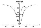
ところで、上記した第一の共振器5_1(図2参照)において、ミラーM1の反射率を「R1」とし、その他のミラー(M2乃至M4)や素子8を経た周回の後に再びミラーM1に戻る直前までの合成反射率を「Rm」と記すとき、共振器の光路が良好に調整された状態となっている場合に、ミラーM1から光を入射した場合における共振器全体の反射光は、光検出器6_1により検出され、その反射率(これを「R(δ)」と記す。)が下式で与えられる。
【0040】
【数1】
尚、上式中の「δ」については、「δ=2π・L1/λ」である。ここで、「λ」は光源の波長、「L1」は共振器の周回光路長をそれぞれ示している。「R1=Rm」のときにインピーダンスマッチング(整合)がとれた状態になる。
【0042】
図4は上式に従う反射特性(δ依存性)を例示したグラフ図であり、横軸に上記「δ」をとり、縦軸に相対反射率(0乃至1)をとって両者の関係を示したものである。尚、グラフ曲線については、見易さを考慮して「R1=Rm=0.90」とし、かつフィネスを実際よりも低めに設定している。
【0043】
[数1]式中に正弦関数sin(δ/2)の二乗項が含まれていることから分かるように、「δ=p・π」(pは偶数)のときに、共振器5_1のみかけの反射率が低下して、入射光が当該共振器内に入って内部の光強度が大きくなる。これを「共振状態」と呼び、共振状態を保持させることを「ロックする」という。
【0044】
振動や温度変化等の外乱に対して、共振器長が「δ=2・π・L1/λ=p・π」の条件を満たすように維持するためには、光路長L1の可変制御手段が必要とされる。そのためには、ミラー(例えば、図2のM3、m3を参照。)や光学素子の位置等を変化させたり、あるいは電気光学素子を用いてその屈折率等を変化させれば良い。例えば、PZT、VCM、ステッピングモータ等を用いた移動手段や駆動手段が挙げられる。
【0045】
共振器の光路長を変化させることでδの値を変化させる場合の、許容周波数半値全幅(半値幅を「δ0.5」と記すとき、その2倍、「2δ0.5」である。)については、共振器のみかけの反射率に係る減少分が、そのピーク点(δ=0、2π等)での値の半分となる値から求められ、おおよそ下式で与えられる。
【0046】
【数2】
尚、これは共振器のみかけの透過率がピーク点での値の半分になるδからも求められる。
【0048】
図5は、相対透過率のδ依存性を例示したグラフ図であり、横軸に上記「δ」をとり、縦軸に相対透過率(0乃至1)をとって両者の関係を示したものである。尚、グラフ曲線については、見易さを考慮して「R1=Rm=0.90」とし、かつフィネスを実際よりも低めに設定している。
【0049】
図に矢印で示すように、相対透過率がそのピーク値の1/2を示すポイントがピークの両側に現れるが、両ポイント間のδ値の差(幅)が許容周波数の半値全幅「2・δ0.5」である。
【0050】
FMサイドバンド法において共振器5_1からの反射光を用いる場合には、上記変調信号の周波数f1について透過半幅「δ0.5」よりも大きくとるのが有利である。
【0051】
図6は相対反射率のδ依存性を示すもので、図4におけるδ=0の付近を拡大して示したものである。
【0052】
図示するように、半値全幅「2δ0.5」の示す範囲(相対反射率0.5以下の範囲)では、相対反射率が急激に低下する傾向が認められるので、反射光を検出する場合に、周波数f1を当該範囲内に設定したのでは光が透過してしまい都合が悪い。
【0053】
図7は、光検出信号及び変調信号に基いて生成される誤差信号(Err)の一例(δ依存性)を拡大して示したものであり、横軸に「δ」をとり、縦軸に信号値(相対値を示し、スケールは任意であり、値そのものに特別な意味はない。)をとって示している。
【0054】
誤差信号Errは、共振器の共振周波数がレーザー光の周波数付近に近づいたときに、反射する両側帯波信号(両側波)のバランスに基づいて得られる信号であり、共振位置(δ=0)からのずれに関してその方向と大きさを示している。つまり、図7の右半面においては、δ軸を正方向に進んでいくと値が上昇しての正のピーク値に達し、それから急に値が低下してボトム値を示してからδ軸に漸近していく。また、図7の左半面においては、δ軸を負方向に進んでいくと値が低下してボトム値に達し、それから急に値が上昇してピーク値を示してからδ軸に漸近していく。このように、グラフ曲線がδ=0の原点回りに180゜の回転対称性をほぼ有しているので、共振位置からのずれの方向と大きさを誤差信号から把握することができる。
【0055】
よって、共振器の構成要素(ミラー等)の位置修正等を行うための負のフィードバック系を、上記制御回路において形成し(誤差がゼロになるように制御を行う。)、共振器の光路長を制御すれば、その共振状態を保つことができる。尚、反射光にサイドバンド(側波帯の成分)がなくべく多く含まれるようにすると、誤差信号の振幅が大きくなり、信号対雑音(S/N)比を一般に大きくすることができる。
【0056】
第一の共振器5_1内の非線形光学素子8については、例えば、KTP、BBO、LBO、LiNbO3等が用いられる。また、近年開発されている、Periodically-Poled Crystals(例えば、PP−KTP、PP−LiNbO3等)を使うこともできる。波長変換素子を用いる場合には、レーザー光源により出力される第一の波長のレーザー光に対して、当該素子によって波長変換された第二の波長のレーザー光が第一の共振器5_1から出力された後に、第二の共振器5_2に入射される。つまり、基本波(例えば、λ=1064nm)に対して、共振により巡回パワーが高くなって波長変換された出力光が上記LT6(図2参照)に相当する。
【0057】
波長変換例として、第二高調波発生(SHG)用に位相整合のとれた結晶、又は分極反転等の手段で位相整合のとれた結晶を素子8として用いる場合には、基本波の波長に対して半分の波長(例えば、λ=532nm)に変換することができる。
【0058】
第一の共振器の出力光(図2のLT6を参照)については、必要に応じてミラー13(波長分離ミラー)等により波長変換されなかった光と分離される。
【0059】
尚、非線形光学素子8により波長変換された基本波成分も、基本波についての損失となることから、上式の反射率「Rm」に関して波長変換効率も考慮して計算する必要がある(William Kozlovsky他, IEEE Journal of Quantum Electronics,Vol.24,No.6,p.913(1988))。
【0060】
また、第一の共振器5_1について共振状態を維持するには、例えば、光検出器6_1による検出出力を低周波成分と高周波成分とに分け、高周波成分を図3の検波部17に送るとともに、当該検波部には、変調信号の周波数f1と等しい周波数信号を信号発生部7(内の局部発振器)から供給して、両者の位相について同期検波を行えば、誤差信号Errが得られる。ミラーM3を駆動するサーボ制御部18は、共振器長の制御手段を構成しており(正確には光路長L1の制御手段である。)、上記したように誤差信号に基いて共振器をロックすることができる。
【0061】
図2のミラー13、14や光学系15は、第一の共振器5_1の出力光LT6を、第二の共振器5_2の空間モードに合わせ込むための調整用に使用することができ、光学系15を経た光は、第二の共振器5_2の入射ミラーm1に入射される。
【0062】
第二の共振器5_2に係る特性について、基本的には共振器5_1と同様であり、ミラーm1の反射率を「r1」とし、その他のミラーや素子を周回して再びミラーm1に戻る直前までの合成反射率を「rm」とすると、共振器の光路が良好に調整されている場合には、ミラーm1から光が入射された共振器全体の反射率は、上記[数1]式において、「R1」を「r1」に、「Rm」を「rm」にそれぞれ置換した式(δについては、勿論、第二の共振器の周回光路長L2や入力光波長等を使用する必要がある。)で与えられ、例えば、「r1=rm」のときにインピーダンスマッチングがとれた状態になる。
【0063】
共振器5_2内に置かれた非線形光学素子16として、例えば、第二高調波発生用の結晶(BBO、CLBO、LB4等)を用いた場合には、共振器の入力光(例えば、λ=532nm)の一部が、半分の波長(266nm)に変換されて図2に示す光LT7として出力される。尚、このような波長変換を行う場合には、変換効率を考慮して「rm」を計算する必要がある。
【0064】
第二の共振器について共振状態を維持するには、上記第一の共振器に関する説明において変調信号の周波数「f1」を「f2」に置き換えて適宜に読み替えを行えば良い。つまり、光検出器6_2による検出出力を低周波成分と高周波成分とに分け、高周波成分を検波部17に送るとともに、変調信号の周波数f2と等しい周波数信号を信号発生部(局部発振器)7から検波部17に供給して、両者の位相について同期検波を行えば、誤差信号Errが得られる。ミラーm3を駆動するサーボ制御部18は、共振器長の制御手段(正確には光路長L2の制御手段)を構成しており、誤差信号Errに基いて共振器をロックすることができる。
【0065】
図8は、各共振器の反射率の周波数依存性と、変調周波数の関係について示したものであり、(A)図が第一の共振器5_1に係る相対反射率の入射波長依存性を示し、(B)図が第二の共振器5_2に係る相対反射率の入射波長依存性を示し、(C)図は位相変調器3によって変調を受けて共振器5_1に入射する光のスペクトラムをそれぞれ示している。尚、(A)図、B(図)については、特定の波長周辺に限って考えているので、横軸は周波数を表している。また、(C)図には、説明の簡単化を優先し、光の周波数を「f0」(=c/λ、cは光速度。)とし、当該周波数と上記周波数f1、f2との和周波、差周波のみを示しており(図示の便宜上、線幅を太く示しているが、特に意味はない。)、f1とf2の和周波、差周波等を表示していないが、同期検波の際に用いる信号発生部(局部発振器)の周波数を適宜に選択することで、変調光の含まれる所望の変調周波数のみを選ぶことができることを考慮している。また、周波数「f0」が共振器の透過帯域の中央に示されているが、これは説明の簡単化のためである(通常はロッキングを行わない限り、このような位置には固定されない。)。
【0066】
(A)図と(B)図との比較から分かるように、この例では透過幅に関して、第一の共振器の方が、第二の共振器よりも広くなっている。
【0067】
(C)図において、f0の右脇には、上方に延びる線でそれぞれ示すように、f2による周波数「f0+f2」の上側波が位置され、これからやや離れたところに、f1による周波数「f0+f1」の上側波が位置されている。また、f0の左脇には、下方に延びる線でそれぞれ示すように、周波数「f0−f2」の下側波が位置され、これからやや離れたところに周波数「f0−f1」の下側波が位置されている。
【0068】
第一の共振器5_1において、周波数「f0+f1」や「f0−f1」は透過帯域の外側に位置するので、変調された光成分はほとんど透過せずに反射されてしまう。つまり、第一の共振器を透過しないような周波数f1を用いて位相変調を行えば、第一の共振器からの反射光を取り出して(f0±f1)、S/N比の高い、FMサイドバンド法の誤差信号を得ることができる。
【0069】
また、位相変調器3においてf1よりも周波数の低いf2で変調された光成分については、第一の共振器5_1がロックしたときに透過率が高いので、かなりの部分が第一の共振器に入射される。例えば、図2に示す非線形光学素子8が第二高調波発生用結晶であるとし、基本波の波長に対してその半分である波長の光が発生する場合に、高い割合の位相変調成分についても第一の共振器内に入射されて、波長変換を受けることになる。このときキャリア(搬送波)である光の周波数f0(=c/λ)と、変調信号の周波数f2とが干渉して、f0の周囲にf0±f2の側波が発生する。そして、これらが第二の共振器5_2において反射率の高い周波数であれば、当該共振器から当該成分を含む反射光を取り出して、誤差信号を得ることができる。即ち、周波数f2については、「f0±f2」の光成分が第一の共振器5_1をほぼ透過するが、第二の共振器5_2では反射されるように選ばれており、これを第二の共振器のロックに用いることができる。
【0070】
従って、上記のように波長変換を行う場合に、レーザー光源により出力される光の波長を「第一の波長」とし、第一の共振器内の非線形光学素子によって波長変換された光の波長を「第二の波長」として、当該波長の光が第二の共振器に入射されるとき、第一の波長のレーザー光についてはその反射光を利用して誤差信号を得て第一の共振器をロックするとともに、第二の波長のレーザー光については、その反射光を利用して誤差信号を得て第二の共振器を同時にロックすることができる。
【0071】
このように、図2ではレーザー光源2に対して、2段階の外部共振器5_1、5_2を設けるとともに、FMサイドバンド法を用いて各共振器を共振状態に保つことができ、しかも、そのために、各共振器の前段に位相変調器をそれぞれ配置させる必要がなく、第一の共振器5_1の前段に配置される一つの位相変調器3だけで済むことになる。但し、その際に望ましい変調周波数の割り当てに関して、上記したように、周波数f1により変調を受けた光が第一の共振器5_1で反射されること、そして、周波数f2により変調を受けた光が第一の共振器5_1を透過し、かつ波長変換後に第二の共振器5_2で反射されることが望ましく、そのときには2段階の共振器においてそれぞれの反射光を利用して誤差信号を生成することができる。尚、反射光を用いることにより制御に必要な信号を大きくとれるので、透過光を用いる場合よりも有利なロッキングが可能になる。
【0072】
上記の説明では、各共振器についての、より安定したロッキングを実現するために、異なる周波数f1、f2の変調信号を用いたが、これに限らず、単一周波数の変調信号を用いて、当該信号を位相変調器3に印加するようにした構成でも良い(構成の簡単化やコスト面で有利となる。)。即ち、変調を受けた光について、側波の一部が第一の共振器で反射されること、そして、他の側波が第一の共振器を透過し、かつ波長変換後に第二の共振器で反射されるという条件を満たせば良い。
【0073】
また、信号発生部7により発生される変調信号については、第一の共振器について共振状態を保持するために用いる誤差信号を生成するのに必要な第一の周波数成分と、第二の共振器について共振状態を保持するために用いる誤差信号を生成するのに必要な第二の周波数成分を有しているか、又はこれらの周波数成分を和周波若しくは差周波あるいは高調波の成分として含むように規定されていれば、如何なる周波数を用いても構わない。
【0074】
尚、混変調の際に発生する可能性のある和周波や差周波が原信号と干渉しないためには、第一の共振器と第二の共振器とでそれぞれ使用する位相変調の周波数が、互いに他方の高調波でないこと、さらには周波数の比が、例えば10桁以下の整数比として表されないこと等が望ましい(これらの事項は周波数の選択に際して有効である。)。また、和周波数や差周波数が、原信号の周波数と異なるように設定した場合において、これらの和周波や差周波を用いて誤差信号を生成することも可能である。
【0075】
位相変調器については、上記のように1つの位相変調器を、第一の共振器よりも手前に配置してこれに変調信号に印加する方法と、複数の位相変調器を設けるとともに、そのうちのいずれかに変調信号を印加する方法とが挙げられるが、構成の簡単化の観点からは前者が好ましい。
【0076】
異なる周波数(例えば、f1、f2)を用いる場合に、第一の周波数成分が第二の周波数成分よりも高周波であること(f1>f2)、また、互いに他方の高調波の関係とならないことが望ましいが、FMサイドバンド法は極めてノイズに強い方法であるため、f1がほぼf2に近い場合(f1≒f2)、あるいはf2がf1より高周波の場合(f1<f2)であっても、上記した2段階のロッキングを行うことができる。但し、これらの場合には、S/N比が下がったり、利得が上がらずに外乱の影響が大きくなること、あるいは利得を無理に上げてもノイズ成分の増加により不安定化を招くこと等の問題に配慮すべきである。
【0077】
本発明は、2以上の共振器を備えたレーザー光発生装置において、それぞれの共振器を同時にロックするための制御に一般化して適用することができるが、各共振器については、例えば、下記に示す形態が挙げられる。
【0078】
(A)第一の共振器の内部に利得媒質を有しており、レ−ザー光を増幅して出力する形態
(B)第一の共振器の内部に配置された非線形光学素子によって、第二高調波又は第三高調波が発生される形態
(C)第二の共振器内に配置された非線形光学素子が光混合用素子とされ、2つのレーザー光の合波による和周波又は差周波の光を発生させる形態。
【0079】
尚、ここで、第一の共振器とは、複数の共振器のいずれかであり、第二の共振器とは、第一の共振器以外の共振器である。
【0080】
先ず、形態(A)は、レ−ザー光を増幅するインジェクションロッキングを行うものである。
【0081】
また、形態(B)について、既述のように、第二高調波発生では、入射波の波長に対して半分の波長変換(あるいは2倍周波数を得ること)が行われ、また、第三高調波発生では、入射波の波長に対して3分の1の波長変換(あるいは3倍周波数を得ること)が行われる。
【0082】
形態(C)では、例えば、2つの(角)周波数ω1、ω2の光を素子に照射して両者の和周波ω(=ω1+ω2)の光を得ることができる。
【0083】
図9は、そのような構成の一例19を示したものであり、2つのレーザー光源2B、2Cと、3つの共振器5_1、5_2、5_3を用いている。
【0084】
単一周波数のレーザー光源2B(例えば、波長λ1=532nm)の出力光は、位相変調器3、モードマッチング用光学系4を経て、第一の共振器5_1に入射される。
【0085】
共振器5_1には、4枚のミラーM1乃至M4と波長変換素子20が設けられていて、M1、素子20、M2が主光路上に配置されている。尚、M1から素子20を介してM2に達した後、ここで反射された光がM3、M4の順に反射されて再びM1に戻る光路が形成されている。また、ミラーM4による反射光の一部がM1を透過して光検出器6_1により検出される。
【0086】
第一の共振器5_1に係る共振器長の制御については、M1乃至M4のうち、少なくとも1つにPZTやVCM等の移動手段及び可動機構が設けられている。
【0087】
第一の共振器5_1の出力光LT6は、波長分離ミラー21で2分されて、その一方が受光部22に送られる。尚、受光部22には、光検出器(監視用等。)又はビームダンプ(減衰器)が用いられる。また、波長分離ミラー21で分かれた他方の光がモードマッチング用光学系23を経て第二の共振器5_2に入射される。
【0088】
第二の共振器5_2には、4枚のミラーm1乃至m4及び和周波混合用の素子24が設けられている。即ち、m1から入射された光が、m2、m3で順次反射されてから、素子24を経た後、m4で反射されて再びM1に戻る光路が形成されている。また、ミラーm4による反射光の一部がm1を透過して光検出器6_2により検出される。そして、第二の共振器5_2に係る共振器長の制御を行うために、m1乃至m4のうち、少なくとも1つにPZTやVCM等の移動手段及び可動機構が設けられている。
【0089】
単一周波数のレーザー光源2C(例えば、波長λ2=750nm)の出力光は、位相変調器25で変調を受けてから、モードマッチング用光学系26を経て第三の共振器5_3に入射される。
【0090】
第三の共振器5_3には、4枚のミラーk1乃至k4及び素子24が設けられており、素子24が共振器5_2との間で共有されている。
【0091】
共振器5_3において、ミラーk1に入射された光は、k2、k3で順次反射されてから、素子24を経た後、k4で反射されて再びk1に戻る光路が形成されている。また、ミラーk4による反射光の一部がk1を透過して光検出器6_3により検出される。尚、共振器5_3について、その共振器長の制御を行う必然性はないが、当該制御を行う場合には、k1乃至k4のうち、少なくとも1つにPZTやVCM等の移動手段及び可動機構が設けられる。
【0092】
共振器5_1、5_2に係るロッキングのための制御については、既に説明した方法と同様であって、例えば、周波数f1、f2の変調信号を位相変調器3に印加するとともに、f1の信号による光の変調成分が第一の共振器5_1で反射されるようにし、f2の信号による光の変調成分が第一の共振器5_1を透過して第二の共振器5_2で反射されるようにする。そして、共振器5_1のミラーM4で反射された光を光検出器6_1で検出するとともに、共振器5_2のミラーm4で反射された光を光検出器6_2で検出し、同期検波によってそれぞれの誤差信号を得て、各共振器長を可動ミラーの制御により変化させれば良い。勿論、f1、f2ではなく単一周波数の変調信号を位相変調器3に印加しても良い。また、位相変調器3と25にそれぞれ印加する変調信号の周波数については、両者を独立に決めて、共振器5_2、5_3を各別にロックしても良いし、また、周波数を同じにして同一の局部発振器を使っても良い。
【0093】
本構成では、第一の共振器5_1内の波長変換素子20による第二高調波発生の結果、当該共振器の出力光LT6の波長が基本波の波長の半分(λ1/2=266nm)となる。
【0094】
そして、レーザー光源2Cから光と上記LT6が光混合用の素子20において、周波数加算された結果、当該素子から出力光LT8が得られる。光LT6の波長を改めて「λ1」と記すとき、光LT8の波長(λ)は、「ω=ω1+ω2」を波長についての関係式に書き直した、「1/λ=1/λ1+1/λ2」において、λ1=266(第二高調波)、λ2=750をそれぞれ代入することにより求まり、λが約196nmとなる。
【0095】
このように、レーザー光は、変調信号が印加された位相変調器を透過した後に、第一の共振器内に配置された非線形光学素子によって波長変換され、その後に、他の位相変調器を経ることなく、複数の共振器(例えば、縦列配置とされた共振器)に順次に入射されるようにした構成を用いることができる。そして、この場合にも、変調信号及び各共振器に係る光検出信号から生成される誤差信号を用いたFMサイドバンド法により各共振器を同時に共振状態に保つことができる。
【0096】
尚、図9に示す構成において、レーザー光源2Cを用いずに、レーザー光源2Bの出力光を用いて第三の共振器5_3に入射させると、和周波発生による3倍周波数の出力光を得ることができる。
【0097】
例えば、レーザー光源2Bから位相変調器3を経た光を、ハーフミラー等によって2分し、その一方の光についてはモードマッチング用光学系4を介して第一の共振器5_1に入射させ、他方の光については、モードマッチング用光学系26あるいは位相変調器25及びモードマッチング用光学系26を介して第三の共振器5_3に入射させる。第一の共振器5_1内の素子20により、基本周波数(ω)の2倍の周波数(2ω)が得られ、和周波混合用の素子24により、さら「ω+2ω=3ω」の周波数が得られるので、出力光LT8の波長はレーザー光源2Bによる元の波長に対して3分の1となる(例えば、532/3≒177nm)。
【0098】
尚、この場合に使用する位相変調器については、1つの位相変調器3を、第一及び第二の共振器あるいは第一乃至第三の共振器に対して共通に用いても良いし、また、第一及び第二の共振器に対して位相変調器3を用い、第三の共振器に対して位相変調器25を専用に用いても良い。そして、各共振器をロックするための制御に用いる変調信号の周波数については、それぞれの共振器に対して異なる周波数を用いても良いし、また、2以上の共振器に対して同一の周波数を用いても良い。
【0099】
この他にも、各種の形態で本発明を実施することができるが、複数の共振器に係る透過帯域の幅に関しては、上記第一の共振器の透過幅が第二の共振器の透過幅よりも広い設定にされていることが好ましい(図8(A)、(B)を参照。)。
【0100】
また、第二の共振器の共振状態を保持するために用いられる位相変調信号の周波数f2を、第一の共振器の透過幅に相当する周波数(これを「Δ1」と記す。)とほぼ同等か又はこれよりも低周波とし、かつ、第二の共振器の透過幅に相当する周波数(これを「Δ2」と記す。)とほぼ同等か又はこれよりも高周波とする。つまり、「f2≦Δ1」は、f2による側波が第一の共振器をほぼ透過するための条件であり、「f2≧Δ2」は側波が第二の共振器においてほぼ反射されるための条件である。
【0101】
そして、「f1≧Δ1」、「f2≦Δ1」が好ましいが、前者は、周波数f1による側波が、第一の共振器の透過帯の外側帯域に存在するための条件であり、後者は、周波数f2による側波が、第一の共振器の透過帯域内にあるための条件である。
【0102】
共振器の安定したロッキングのためには、複数の変調周波数又はそれらの和周波信号若しくは差周波信号の各々が、対応する変調信号の周波数(信号発生部7による発振周波数)に対して安定した位相関係にあることが必要である。そのためには、同期検波の際にそれぞれの変調周波数に対して独立に位相遅延量を調整できるようにすることが好ましい。例えば、図3において、光検出器6_1、6_2と検波部17との間に遅延(ディレイ)回路を介挿して、光検出信号の位相遅延について調整を行えるように構成すれば良い。
【0103】
しかして、本発明では、位相変調されたレーザー光を第一の共振器に入射させた後、当該共振器中に配置された非線形光学素子により発生される光を、位相変調器を経ることなく第二の共振器に入射させ、そして、第一及び第二の共振器からの光をそれぞれ検出するとともに、各検出信号及び変調信号から誤差信号を生成して、共振器毎にそれぞれの光路長を制御することにより、複数の共振器を同時に共振状態に保つことができる。
【0104】
従って、下記に示す各種の利点が得られる。
【0105】
・従来よりも少ない数の位相変調器を用いて、複数の共振器をFMサイドバンド法で安定にロックすることができるため、装置構成が簡素化され、小型化やコストの低減に好適である。
【0106】
・紫外光や紫外線への適用において有用である。例えば、上記第一の共振器により波長変換された出力光の波長が400nm以下である場合において、高性能な位相変調器を使う必要がない。つまり、紫外線等の変調に利用できる位相変調器については、高電圧を必要としたり、素子サイズが大きいこと、電源を含めたコストが嵩むといった不都合を伴い、素子の入手経路が限られてしまうが、上記の構成では、このような問題は一切なく、安価で使い易い位相変調器で済むため、コストの低減が可能となり、また、装置の製造に要する時間を短縮できる。
【0107】
・効率の上昇や小型化に適した構成及び方法を提供でき、消費電力の低減や配置スペースの低減にとって有効である。
【0108】
【発明の効果】
以上に記載したところから明らかなように、請求項1や請求項16に係る発明によれば、FMサイドバンド法を用いることで共振器の安定なロッキングが可能となることは勿論、各共振器に対してそれぞれの前段に位相変調器を設ける必要がないので、従来よりも少ない数の位相変調器を用いて複数の共振器を同時にロックすることができる。また、紫外線等への適用において、特別な位相変調を用いる必要がない。
【0109】
請求項2や請求項17に係る発明によれば、異なる周波数の変調信号を用いることによって各共振器をより安定にロックすることができる。
【0110】
請求項3乃至6や、請求項18及び19に係る発明によれば、非線形光学素子の温度変化等による影響を受け難いので、当該素子を使った波長変換をより安定して効率良く行うことができる。
【0111】
請求項7や請求項20、21に係る発明によれば、各共振器に対応する周波数成分をもった信号を使って、それぞれの共振器を同時にロックすることができる。
【0112】
請求項8や請求項22に係る発明によれば、信号対ノイズ比が高く、外乱に対して安定したロッキングが可能になる。
【0113】
請求項9に係る発明によれば、レーザー光の増幅により所望の出力を得ることができる。
【0114】
請求項10に係る発明によれば、高調波発生により短波長の出力光を得ることができる。
【0115】
請求項11に係る発明によれば、和周波や差周波の発生により各種波長の出力光を得ることができる。
【0116】
請求項12や請求項23に係る発明によれば、位相変調器を経ることなく配置された共振器に対して順次にレーザー光を入射させて各共振器を同時にロックすることができ、光量の損失が少なく効率が良い。
【0117】
請求項13乃至15、請求項24乃至26によれば、第一の共振器と第二の共振器について、それぞれの変調周波数を区別して使用できるとともに、反射光の検出信号を用いて誤差信号を得ることができるので、共振器のロッキングにとって有利である。
【図面の簡単な説明】
【図1】本発明に係る基本構成例を示す説明図である。
【図2】図3とともに本発明の構成例を示す図であり、本図は全体構成についてその要部を示す。
【図3】位相変調器及び光検出器を含む制御系の構成例を示す図である。
【図4】相対反射率のδ依存性を示すグラフ図である。
【図5】相対透過率のδ依存性を示すグラフ図である。
【図6】相対反射率のδ依存性について要部を拡大して示す図である。
【図7】誤差信号のδ依存性を示す図である。
【図8】反射率の周波数依存性と変調周波数との関係について説明するための図である。
【図9】本発明に係る別の構成例を示す図である。
【符号の説明】
1、12、19…レーザー光発生装置、2、2A、2B、2C…レーザー光源、3、25…位相変調器、4、15、23、26…光学系、5_1…第一の共振器、5_2…第二の共振器、6_X(X=1、2、…)…光検出器、7…信号発生部、8、20…非線形光学素子、9…光路長可変手段、11…制御回路[0001]
BACKGROUND OF THE INVENTION
The present invention relates to a technique for realizing stable locking using a cross-modulated carrier in a laser beam generator using a laser light source and a plurality of resonators.
[0002]
[Prior art]
The FM sideband method (“Pound-Drever-Hall Locking” method) is known as a stable resonator locking method in laser light generators, and is used to lock external resonators from near infrared to visible light. Widely used.
[0003]
In addition to this method, there is a method using polarized light (see documents such as Hansch, Couillaud, Optics Communications, 1980). For example, a laser beam that has passed through a wave plate is incident on a resonator, and an error signal is obtained based on detection signals of two beams having different polarization states from the resonator, and locking that maintains the resonance state of the resonator. A method has been proposed.
[0004]
[Problems to be solved by the invention]
However, the conventional apparatus has the following problems.
[0005]
-In the polarization method, etc., due to heat generation when there is a change in the amount of light incident on the resonator, or when an optical element that absorbs light (especially an element that absorbs light in the ultraviolet region) is included in the resonator A wavelength offset is likely to occur because the characteristics of the optical element change with a change in temperature and the phase delay amount changes, and there is a problem in stability.
[0006]
-In the method called FM sideband method or "Pound-Drever-Hall Locking" method, it is necessary to make a side wave (sideband) using a phase modulator to generate an error signal. What is required for modulating the side wave is a high-performance phase modulator that has high transmittance and low operating voltage. However, since it is difficult to obtain such a modulator, when an available phase modulator is used, a circuit or the like for driving a high voltage and high frequency is required, which causes an increase in cost and power consumption. There are disadvantages such as these and problems in practicality.
[0007]
・ When locking each resonator at the same time in a configuration using multiple resonators, if the number of resonators increases, the number of phase modulators arranged at each stage also increases, which increases the size of the device. Or cause an increase in cost. This is because in the conventional configuration, the phase modulator is arranged in front of each resonator, and the arrangement space for that is increased.
[0008]
Therefore, an object of the present invention is to realize stable locking in a laser beam generator provided with a plurality of resonators, and to prevent an increase in cost and an increase in power consumption.
[0009]
[Means for Solving the Problems]
In order to solve the above-described problems, a laser beam generator according to the present invention includes the following components.
[0010]
・ Laser light source that outputs laser light
A phase modulator and a signal generator that generates a modulation signal to be applied to the phase modulator
A plurality of resonators including a first resonator and a second resonator disposed downstream of the resonator;
.Nonlinear optical elements arranged in the first resonator
.Optical path length variable means for changing the optical path length of each resonator
An optical system that is arranged between the laser light source and the resonator and between the two resonators to couple them together
・ A photodetector that receives light from each resonator
An error signal is obtained from a detection signal and a modulation signal obtained by each photodetector, and an optical path length variable means according to an FM (frequency modulation) sideband method (“Pound-Drever-Hall Locking” method) using the error signal. A control circuit having a negative feedback configuration for controlling the current.
[0011]
The laser light is incident on the phase modulator and applied with phase modulation and then incident on the first resonator, and the light generated by the nonlinear optical element is incident on the second resonator. In this configuration, the light from the first and second resonators is detected by the photodetector, and the optical path length is controlled for each resonator based on the error signal. It is intended to be kept in a state.
[0012]
In the laser light generation method according to the present invention, after the phase-modulated laser light is incident on the first resonator, the light generated by the nonlinear optical element disposed in the resonator is transmitted to the second resonator. By entering the resonator and detecting light from the first and second resonators respectively, and generating an error signal from each detection signal and modulation signal, and controlling the respective optical path lengths for each resonator. A plurality of resonators are simultaneously held in a resonance state.
[0013]
Therefore, according to the present invention, it is possible to stably lock the resonator by using the FM sideband method, and it is not necessary to provide a phase modulator in the previous stage for each resonator. A plurality of resonators can be locked simultaneously using a smaller number of phase modulators than in the conventional configuration.
[0014]
DETAILED DESCRIPTION OF THE INVENTION
The present invention relates to a laser light source using a laser light source capable of continuous oscillation (CW) and a plurality of resonators, and is suitable for application to wavelength conversion in a plurality of stages, for example.
[0015]
FIG. 1 is a diagram for conceptually explaining an example of the basic configuration of the present invention.
[0016]
The
[0017]
The laser light is sent to a plurality of resonators 5_X (X = 1, 2,..., N) through the
[0018]
The plurality of resonators 5_X (X = 1, 2,..., N) are arranged in tandem, and are arranged at a stage subsequent to the first resonator (for example, “5_1”) and the resonator. A second resonator (for example, this is referred to as “5_2”) is included. Note that the first resonator does not necessarily have to be the first-stage resonator, and any resonator may be used, and the second resonator may be positioned downstream from the first resonator. Any resonator can be used. However, a nonlinear optical element (or nonlinear optical crystal) 8 is disposed in the first resonator. For example, there are elements for wavelength conversion related to second harmonic generation, sum frequency generation, etc., but other elements (such as recording elements) can also be used.
[0019]
Among the resonators, at least the first and second resonators are provided with optical path length varying means 9 for changing the optical path length, for example, a constituent element of the resonator (mirror or optical element). Is controlled using an actuator such as a VCM (voice coil motor), a piezoelectric element, or the like, or a voltage or the like is applied to the crystal to control optical characteristics (refractive index, etc.).
[0020]
Note that mode matching
[0021]
The photodetector 6_X (X = 1, 2,..., N) is provided to receive light from each resonator. In addition, although the form which detects the reflected light from a resonator, and the form which detects the transmitted light of a resonator are mentioned, the former form is preferable from a viewpoint of the magnitude | size of a detection signal.
[0022]
The
[0023]
In this configuration, the laser light emitted from the
[0024]
Light (reflected light or transmitted light) from the first resonator or the second resonator is detected by the photodetectors 6_1 and 6_2, respectively, and is based on each error signal obtained by detection by the
[0025]
The modulation signal applied to the
[0026]
FIG. 2 shows an example 12 in which one phase modulator is used so that two-stage wavelength conversion resonators can be locked simultaneously by the FM sideband method.
[0027]
In this example, a
[0028]
The light transmitted through the
[0029]
The resonator 5_1 includes an incident mirror M1, a plurality of mirrors M2, M3, M4 and a nonlinear
[0030]
A part of the reflected light from the mirror M4 passes through M1, and then is received by the photodetector 6_1 to perform signal detection.
[0031]
The output light LT6 of the resonator 5_1 is reflected by the
[0032]
The resonator 5_2 is configured using, for example, the incident mirror m1, a plurality of mirrors m2, m3, and m4 and the nonlinear
[0033]
Part of the reflected light from the mirror m4 is transmitted through m1 and then received by the photodetector 6_2 to perform signal detection.
[0034]
The light LT7 emitted from the mirror m2 is emitted to the outside as output light of the resonator 5_2.
[0035]
FIG. 3 shows a basic configuration example of a control system including a phase modulator and a photodetector. In addition, since it is set as the same circuit structure about the 1st and 2nd resonator, the part common to both circuits is shown collectively in the figure.
[0036]
The
[0037]
The detection signal by the photodetector (in the example shown, the photodetector 6_1 for the first resonator and the photodetector 6_2 for the second resonator) and the modulation signal (frequency for the first resonator). The signal of f1 and the signal of frequency f2 for the second resonator) are sent to the detector 17 (shown as a multiplier as a multiplier in the figure) to perform synchronous detection, and the error obtained thereby A signal (referred to as “Err”) is sent to the servo control unit 18. In addition, although not shown in the figure, a so-called “Pull-in” circuit that determines whether or not to perform locking based on a signal from the total light amount monitor may be attached.
[0038]
The servo control unit 18 generates a control signal so that the level of the error signal Err becomes zero, and controls the optical path length of the resonator by the signal. That is, in the example of FIG. 2, the position and orientation of the mirror M3 are controlled by the first resonator 5_1, and the position and orientation of the mirror m3 are controlled by the second resonator 5_2. It should be noted that a well-known mechanism may be used for the mirror moving mechanism, the drive control circuit, etc., and further description thereof will be omitted. Further, illustration of a circuit necessary for signal processing, for example, a filter necessary for extracting a high-frequency signal from a detection signal after light reception is omitted (or may be considered to be included in a photodetector or the like). Only the basic elements of processing are shown.
[0039]
By the way, in the first resonator 5_1 (see FIG. 2), the reflectance of the mirror M1 is set to “R”.1 ”, And the combined reflectivity until“ R ”after returning to the mirror M1 after the circulation through the other mirrors (M2 to M4) and the
[0040]
[Expression 1]
For “δ” in the above formula, “δ = 2π · L1 / Λ ". Here, “λ” is the wavelength of the light source, “L”1 "Indicates the optical path length of the resonator. "R1 = Rm ", Impedance matching (matching) is achieved.
[0042]
FIG. 4 is a graph illustrating the reflection characteristics (δ dependency) according to the above equation, where the horizontal axis indicates “δ” and the vertical axis indicates the relative reflectance (0 to 1) and shows the relationship between the two. It is a thing. Note that the graph curve is “R” for ease of viewing.1 = Rm = 0.90 "and the finesse is set lower than actual.
[0043]
As can be seen from the fact that the square term of the sine function sin (δ / 2) is included in the equation (1), only the resonator 5_1 is multiplied when “δ = p · π” (p is an even number). , The incident light enters the resonator and the light intensity inside increases. This is called “resonance state”, and holding the resonance state is called “locking”.
[0044]
The resonator length is “δ = 2 · π · L against disturbances such as vibration and temperature change.1 In order to maintain the condition of “/ λ = p · π”, the optical path length L1 Variable control means are required. For this purpose, the position of the mirror (for example, see M3 and m3 in FIG. 2) and the optical element may be changed, or the refractive index thereof may be changed using an electro-optical element. For example, moving means and driving means using PZT, VCM, stepping motor and the like can be mentioned.
[0045]
When changing the value of δ by changing the optical path length of the resonator, the full width at half maximum of the allowable frequency (the half width at “δ0.5 "Is twice that," 2δ0.5 Is. ) Is obtained from a value that is a half of the value at the peak point (δ = 0, 2π, etc.), and is approximately given by the following equation.
[0046]
[Expression 2]
This can also be obtained from δ at which the apparent transmittance of the resonator is half the value at the peak point.
[0048]
FIG. 5 is a graph illustrating the dependence of relative transmittance on δ. The horizontal axis represents the above-mentioned “δ”, and the vertical axis represents the relative transmittance (0 to 1). It is. Note that the graph curve is “R” for ease of viewing.1 = Rm = 0.90 "and the finesse is set lower than actual.
[0049]
As shown by the arrows in the figure, the point where the relative transmittance is 1/2 of the peak value appears on both sides of the peak, but the difference (width) of the δ value between the two points is the full width at half maximum of the allowable frequency “2. δ0.5 Is.
[0050]
When the reflected light from the resonator 5_1 is used in the FM sideband method, the transmission half-width “δ” is obtained for the frequency f1 of the modulation signal.0.5 It is advantageous to take a larger value than
[0051]
FIG. 6 shows the δ dependence of the relative reflectance, and shows an enlarged view of the vicinity of δ = 0 in FIG.
[0052]
As shown in the figure, the full width at half maximum “2δ”0.5 In the range indicated by "(range where the relative reflectance is 0.5 or less), the relative reflectance tends to decrease rapidly. Therefore, when the reflected light is detected, the frequency f1 is not set within the range. It is inconvenient because the light is transmitted.
[0053]
FIG. 7 is an enlarged view of an example (δ dependency) of the error signal (Err) generated based on the photodetection signal and the modulation signal. The horizontal axis indicates “δ”, and the vertical axis indicates The signal value (representing a relative value, the scale is arbitrary, and the value itself has no special meaning) is shown.
[0054]
The error signal Err is a signal obtained based on the balance of the reflected double sideband signals (both side waves) when the resonance frequency of the resonator approaches the frequency of the laser beam, and the resonance position (δ = 0). The direction and size of the deviation from is shown. That is, in the right half of FIG. 7, when the δ-axis is advanced in the positive direction, the value increases to reach a positive peak value, and then suddenly decreases to show the bottom value before the δ-axis. Asymptotically. In the left half of FIG. 7, as the δ axis advances in the negative direction, the value decreases to reach the bottom value, and then suddenly increases to show the peak value and then asymptotically approaches the δ axis. Go. Thus, since the graph curve has a rotational symmetry of 180 ° around the origin of δ = 0, the direction and magnitude of deviation from the resonance position can be grasped from the error signal.
[0055]
Therefore, a negative feedback system for correcting the position of the constituent elements (mirror, etc.) of the resonator is formed in the control circuit (control is performed so that the error becomes zero), and the optical path length of the resonator is set. By controlling this, the resonance state can be maintained. If the reflected light includes as much sideband (sideband component) as possible, the amplitude of the error signal increases and the signal-to-noise (S / N) ratio can generally be increased.
[0056]
For the nonlinear
[0057]
As an example of wavelength conversion, when a crystal that is phase-matched for second harmonic generation (SHG) or a crystal that is phase-matched by means of polarization inversion is used as the
[0058]
The output light of the first resonator (see LT6 in FIG. 2) is separated from the light that has not been wavelength-converted by a mirror 13 (wavelength separation mirror) or the like as necessary.
[0059]
Since the fundamental wave component wavelength-converted by the nonlinear
[0060]
In order to maintain the resonance state of the first resonator 5_1, for example, the detection output by the photodetector 6_1 is divided into a low-frequency component and a high-frequency component, and the high-frequency component is sent to the
[0061]
The
[0062]
The characteristics of the second resonator 5_2 are basically the same as those of the resonator 5_1, and the reflectance of the mirror m1 is “r”.1 ”, And the combined reflectance until just before returning to the mirror m1 after circling other mirrors and elements is“ r ”m When the optical path of the resonator is well adjusted, the reflectance of the entire resonator that is incident with light from the mirror m1 is expressed by “R”1 To "r"1 To "R"m To "r"m , Of course, the optical path length L of the second resonator is, of course, δ.2 And the input light wavelength must be used. ), For example, “r1 = Rm ", Impedance matching is achieved.
[0063]
For example, when a second harmonic generation crystal (BBO, CLBO, LB4, etc.) is used as the nonlinear
[0064]
In order to maintain the resonance state of the second resonator, the frequency “f1” of the modulation signal may be replaced with “f2” in the description relating to the first resonator and read as appropriate. That is, the detection output from the photodetector 6_2 is divided into a low frequency component and a high frequency component, the high frequency component is sent to the
[0065]
FIG. 8 shows the relationship between the frequency dependence of the reflectance of each resonator and the modulation frequency. FIG. 8A shows the incident wavelength dependence of the relative reflectance according to the first resonator 5_1. FIGS. 4A and 4B show the incident wavelength dependence of the relative reflectance of the second resonator 5_2, and FIG. 4C shows the spectrum of light that is modulated by the
[0066]
As can be seen from a comparison between FIGS. (A) and (B), in this example, the first resonator is wider than the second resonator with respect to the transmission width.
[0067]
(C) In the figure, on the right side of f0, as indicated by the line extending upward, the upper wave of the frequency “f0 + f2” by f2 is located, and at a distance from this, the frequency “f0 + f1” by f1 is located. The upper wave is located. Further, on the left side of f0, as shown by the lines extending downward, a lower side wave of the frequency “f0-f2” is located, and a lower side wave of the frequency “f0-f1” is located slightly away from this. Is located.
[0068]
In the first resonator 5_1, the frequencies “f0 + f1” and “f0−f1” are located outside the transmission band, so that the modulated light component is reflected without being transmitted. That is, if phase modulation is performed using a frequency f1 that does not pass through the first resonator, the reflected light from the first resonator is extracted (f0 ± f1), and the FM side with a high S / N ratio is obtained. An error signal of the band method can be obtained.
[0069]
In addition, the light component modulated at f2 having a frequency lower than f1 in the
[0070]
Therefore, when wavelength conversion is performed as described above, the wavelength of the light output from the laser light source is the “first wavelength”, and the wavelength of the light converted by the nonlinear optical element in the first resonator is As the “second wavelength”, when light of the wavelength is incident on the second resonator, an error signal is obtained using the reflected light of the laser light of the first wavelength to obtain the first resonator. The second resonator can be simultaneously locked by obtaining an error signal using the reflected light of the laser light of the second wavelength.
[0071]
As described above, in FIG. 2, the
[0072]
In the above description, in order to realize more stable locking for each resonator, the modulation signals of different frequencies f1 and f2 are used. However, the present invention is not limited to this, and a single frequency modulation signal is used. A configuration may be adopted in which a signal is applied to the phase modulator 3 (which is advantageous in terms of simplification of the configuration and cost). That is, for the modulated light, a part of the side wave is reflected by the first resonator, and the other side wave is transmitted through the first resonator and the second resonance after wavelength conversion. It is sufficient to satisfy the condition of being reflected by a vessel.
[0073]
For the modulation signal generated by the
[0074]
In order to prevent the sum frequency and difference frequency that may occur during intermodulation from interfering with the original signal, the phase modulation frequency used by the first resonator and the second resonator, It is desirable that they are not harmonics of the other, and that the ratio of the frequencies is not expressed as an integer ratio of, for example, 10 digits or less (these matters are effective in selecting the frequency). In addition, when the sum frequency or difference frequency is set to be different from the frequency of the original signal, it is also possible to generate an error signal using these sum frequency and difference frequency.
[0075]
As for the phase modulator, as described above, one phase modulator is disposed in front of the first resonator and applied to the modulation signal, and a plurality of phase modulators are provided. One of them is a method of applying a modulation signal, but the former is preferable from the viewpoint of simplification of the configuration.
[0076]
When different frequencies (for example, f1 and f2) are used, the first frequency component may be higher in frequency than the second frequency component (f1> f2), and may not be related to the other harmonic. Although it is desirable, the FM sideband method is extremely noise-resistant, so even if f1 is almost close to f2 (f1≈f2), or even when f2 is higher in frequency than f1 (f1 <f2), it is described above. Two stages of locking can be performed. However, in these cases, the S / N ratio decreases, the gain does not increase, the influence of disturbance increases, or even if the gain is increased forcibly, destabilization occurs due to an increase in noise components, etc. You should consider the problem.
[0077]
The present invention can be generalized and applied to a control for simultaneously locking each resonator in a laser light generating device including two or more resonators. The form to show is mentioned.
[0078]
(A) A configuration having a gain medium inside the first resonator and amplifying and outputting the laser beam
(B) A mode in which the second harmonic or the third harmonic is generated by the nonlinear optical element disposed inside the first resonator
(C) A mode in which a nonlinear optical element disposed in the second resonator is used as a light mixing element, and generates light of a sum frequency or a difference frequency by combining two laser beams.
[0079]
Here, the first resonator is one of a plurality of resonators, and the second resonator is a resonator other than the first resonator.
[0080]
First, the form (A) performs injection locking for amplifying laser light.
[0081]
As for the form (B), as described above, in the second harmonic generation, half wavelength conversion (or obtaining a double frequency) is performed with respect to the wavelength of the incident wave, and the third harmonic is generated. In wave generation, wavelength conversion of one third (or obtaining a triple frequency) is performed with respect to the wavelength of the incident wave.
[0082]
In the form (C), for example, light having two (angular) frequencies ω1 and ω2 can be irradiated on the element to obtain light having a sum frequency ω (= ω1 + ω2) of both.
[0083]
FIG. 9 shows an example 19 of such a configuration, which uses two
[0084]
Output light of a single-frequency
[0085]
The resonator 5_1 is provided with four mirrors M1 to M4 and a
[0086]
Regarding the control of the resonator length related to the first resonator 5_1, at least one of M1 to M4 is provided with a moving means such as PZT or VCM and a movable mechanism.
[0087]
The output light LT6 of the first resonator 5_1 is divided into two by the
[0088]
The second resonator 5_2 is provided with four mirrors m1 to m4 and a sum
[0089]
The output light of the single-frequency laser light source 2C (for example, wavelength λ2 = 750 nm) is modulated by the
[0090]
The third resonator 5_3 is provided with four mirrors k1 to k4 and an
[0091]
In the resonator 5_3, the light incident on the mirror k1 is sequentially reflected by k2 and k3, passes through the
[0092]
The control for locking related to the resonators 5_1 and 5_2 is the same as the method already described. For example, the modulation signals of the frequencies f1 and f2 are applied to the
[0093]
In this configuration, as a result of the second harmonic generation by the
[0094]
Then, as a result of frequency addition of the light from the
[0095]
As described above, the laser light is transmitted through the phase modulator to which the modulation signal is applied, and then wavelength-converted by the nonlinear optical element disposed in the first resonator, and then passes through another phase modulator. Instead, it is possible to use a configuration in which light is sequentially incident on a plurality of resonators (for example, resonators arranged in cascade). Also in this case, the resonators can be simultaneously kept in the resonance state by the FM sideband method using the error signal generated from the modulation signal and the light detection signal associated with each resonator.
[0096]
In the configuration shown in FIG. 9, when the output light of the
[0097]
For example, the light that has passed through the
[0098]
As for the phase modulator used in this case, one
[0099]
In addition to the above, the present invention can be implemented in various forms. Regarding the width of the transmission band related to a plurality of resonators, the transmission width of the first resonator is the transmission width of the second resonator. It is preferable that the setting is wider (see FIGS. 8A and 8B).
[0100]
Further, the frequency f2 of the phase modulation signal used for maintaining the resonance state of the second resonator is set to a frequency corresponding to the transmission width of the first resonator (this is expressed as “Δ1 ". ) And a frequency corresponding to the transmission width of the second resonator (this is expressed as “Δ”).2 ". ) Or a higher frequency than this. That is, “f2 ≦ Δ1 "Is a condition for the side wave due to f2 to substantially pass through the first resonator, and" f2 ≧ Δ2 "Is a condition for side waves to be substantially reflected at the second resonator.
[0101]
And “f1 ≧ Δ1 ”,“ F2 ≦ Δ1 The former is a condition for the side wave having the frequency f1 to exist in the outer band of the transmission band of the first resonator, and the latter is the condition for the side wave having the frequency f2 to be the first resonator. It is a condition for being in the transmission band of.
[0102]
For stable locking of the resonator, each of a plurality of modulation frequencies or their sum frequency signal or difference frequency signal has a stable phase with respect to the frequency of the corresponding modulation signal (oscillation frequency by the signal generator 7). It needs to be in a relationship. For this purpose, it is preferable that the phase delay amount can be adjusted independently for each modulation frequency during synchronous detection. For example, in FIG. 3, a delay circuit may be inserted between the photodetectors 6_1 and 6_2 and the
[0103]
Thus, in the present invention, after the phase-modulated laser light is incident on the first resonator, the light generated by the nonlinear optical element disposed in the resonator is passed through the phase modulator. The light is incident on the second resonator, and the light from the first and second resonators is detected, and an error signal is generated from each detection signal and the modulation signal. By controlling the above, it is possible to simultaneously maintain a plurality of resonators in the resonance state.
[0104]
Therefore, various advantages shown below can be obtained.
[0105]
Since a plurality of resonators can be stably locked by the FM sideband method using a smaller number of phase modulators than in the past, the device configuration is simplified, which is suitable for downsizing and cost reduction. .
[0106]
-Useful for application to ultraviolet light and ultraviolet light. For example, when the wavelength of the output light wavelength-converted by the first resonator is 400 nm or less, it is not necessary to use a high-performance phase modulator. In other words, the phase modulator that can be used for the modulation of ultraviolet rays or the like has a disadvantage that a high voltage is required, the element size is large, and the cost including the power source is increased, and the element acquisition path is limited. In the above configuration, there is no such problem, and an inexpensive and easy-to-use phase modulator is sufficient. Therefore, the cost can be reduced and the time required for manufacturing the device can be shortened.
[0107]
A configuration and method suitable for increasing efficiency and downsizing can be provided, which is effective for reducing power consumption and arrangement space.
[0108]
【The invention's effect】
As is apparent from the above description, according to the inventions according to
[0109]
According to the inventions according to
[0110]
According to the inventions according to
[0111]
According to the invention which concerns on
[0112]
According to the inventions according to
[0113]
According to the ninth aspect of the invention, a desired output can be obtained by amplification of laser light.
[0114]
According to the invention which concerns on
[0115]
According to the invention which concerns on
[0116]
According to the inventions according to
[0117]
According to the thirteenth to fifteenth and twenty-fourth to twenty-sixth aspects, the first resonator and the second resonator can be used by distinguishing the respective modulation frequencies, and the error signal is generated using the detection signal of the reflected light. This is advantageous for the locking of the resonator.
[Brief description of the drawings]
FIG. 1 is an explanatory diagram showing an example of a basic configuration according to the present invention.
FIG. 2 is a diagram showing a configuration example of the present invention together with FIG. 3, and this drawing shows the main part of the overall configuration.
FIG. 3 is a diagram illustrating a configuration example of a control system including a phase modulator and a photodetector.
FIG. 4 is a graph showing the δ dependency of relative reflectance.
FIG. 5 is a graph showing the δ dependency of relative transmittance.
FIG. 6 is an enlarged view showing a main part of the δ dependence of relative reflectance.
FIG. 7 is a diagram illustrating the δ dependency of an error signal.
FIG. 8 is a diagram for explaining a relationship between a frequency dependency of reflectance and a modulation frequency.
FIG. 9 is a diagram showing another configuration example according to the present invention.
[Explanation of symbols]
DESCRIPTION OF
Claims (24)
Translated fromJapanese第一の共振器及び当該共振器よりも後段に配置される第二の共振器を含む複数の共振器と、
上記レーザー光源と上記第一の共振器との間の光路上に配置された異なる周波数の変調信号が印加される一又は複数の位相変調器及び当該位相変調器に印加する変調信号を生成する信号発生部と、
上記第一の共振器中に配置された非線形光学素子と、各共振器の光路長をそれぞれ変化させるための光路長可変手段と、
上記レーザー光源と共振器との間及び2つの共振器の間に配置されて両者を結合させるための光学系と、
各共振器からの光をそれぞれ受光する光検出器と、
上記光検出器によって得られる検出信号及び上記変調信号から誤差信号を得て、当該誤差信号を用いたFMサイドバンド法に従って上記光路長可変手段を制御するために負帰還の構成を有する制御回路とを備え、
上記レーザー光源から出力されたレーザー光が上記位相変調器に入射されて位相変調を与えられてから上記第一の共振器に入射されるとともに、上記非線形光学素子により発生される光が上記位相変調器を介することなく上記第二の共振器に入射されること、
そして、上記第一及び第二の共振器からの光が上記光検出器によってそれぞれ検出されるとともに、上記誤差信号に基いて共振器毎に光路長が制御されることで、これら複数の共振器が同時に共振状態に保たれることを特徴とするレーザー光発生装置。A laser light source that outputs laser light;
A plurality of resonators including a first resonator and a second resonator disposed downstream of the resonator;
One or a plurality of phase modulatorsarranged on an optical path between the laser light source and the first resonator to which modulation signals of different frequencies are applied , and a signal for generating a modulation signal to be applied to the phase modulator Generating part;
A nonlinear optical element disposed in the first resonator, an optical path length varying means for changing the optical path length of each resonator, and
An optical system disposed between the laser light source and the resonator and between the two resonators for coupling the two;
A photodetector for receiving light from each resonator;
A control circuit having a negative feedback configuration for obtaining an error signal from the detection signal obtained by the photodetector and the modulation signal and controlling the optical path length varying means according to the FM sideband method using the error signal; With
Laser light output from the laser light source is incident on the phase modulator and applied with phase modulation, and then is incident on the first resonator, and light generated by the nonlinear optical element ismodulated with the phase modulation. Being incident on the second resonatorwithout going through the resonator,
The light from the first and second resonators is detected by the photodetector, and the optical path length is controlled for each resonator based on the error signal. Are kept in the resonance state at the same time.
第一の共振器内に配置される非線形光学素子によって波長変換が行われることを特徴とするレーザー光発生装置。In the laser beam generator according to claim 1,
2. A laser beam generator characterized in that wavelength conversion is performed by a nonlinear optical element disposed in a first resonator.
第一の共振器内に配置される非線形光学素子によって波長変換が行われることを特徴とするレーザー光発生装置。In the laser beam generator according to claim1 ,
2. A laser beam generator characterized in that wavelength conversion is performed by a nonlinear optical element disposed in a first resonator.
レーザー光源により出力される第一の波長のレーザー光に対して、非線形光学素子によって波長変換された第二の波長のレーザー光が第二の共振器に入射されるとともに、
第一の波長のレーザー光について第一の共振器が共振状態に保たれ、かつ、第二の波長のレーザー光について第二の共振器が共振状態に保たれるようにしたことを特徴とするレーザー光発生装置。In the laser beam generator according to claim2 ,
With respect to the laser beam of the first wavelength output from the laser light source, the laser beam of the second wavelength converted by the nonlinear optical element is incident on the second resonator,
The first resonator is kept in a resonance state with respect to the laser light having the first wavelength, and the second resonator is kept in a resonance state with respect to the laser light having the second wavelength. Laser light generator.
レーザー光源により出力される第一の波長のレーザー光に対して、非線形光学素子によって波長変換された第二の波長のレーザー光が第二の共振器に入射されるとともに、
第一の波長のレーザー光について第一の共振器が共振状態に保たれ、かつ、第二の波長のレーザー光について第二の共振器が共振状態に保たれるようにしたことを特徴とするレーザー光発生装置。In the laser beam generator according to claim3 ,
With respect to the laser beam of the first wavelength output from the laser light source, the laser beam of the second wavelength converted by the nonlinear optical element is incident on the second resonator,
The first resonator is kept in a resonance state with respect to the laser light having the first wavelength, and the second resonator is kept in a resonance state with respect to the laser light having the second wavelength. Laser light generator.
第一の共振器について共振状態を保持するために用いる誤差信号を生成するのに必要な発振信号に係る第一の周波数成分及び第二の共振器について共振状態を保持するために用いる誤差信号を生成するのに必要な発振信号に係る第二の周波数成分を有する変調信号を信号発生部が発生させて、当該信号を一又は複数の位相変調器のいずれかに印加することを特徴とするレーザー光発生装置。In the laser beam generator according to claim1 ,
The first frequency component related to the oscillation signal necessary for generating the error signal used for maintaining the resonance state for the first resonator and the error signal used for maintaining the resonance state for the second resonator A laser generating a modulation signal having a second frequency component related to an oscillation signal necessary for generation and applying the signal to one or a plurality of phase modulators Light generator.
第一の周波数成分が第二の周波数成分よりも高周波であることを特徴とするレーザー光発生装置。In the laser beam generator according to claim6 ,
A laser light generator characterized in that the first frequency component is higher in frequency than the second frequency component.
第一の共振器が、その内部に利得媒質を有しており、レ−ザー光を増幅して出力することを特徴とするレーザー光発生装置。In the laser beam generator according to claim 1,
A laser light generator characterized in that the first resonator has a gain medium therein and amplifies and outputs the laser beam.
第一の共振器の内部に配置された非線形光学素子によって高調波が発生されることを特徴とするレーザー光発生装置。In the laser beam generator according to claim 1,
Harmonics are generated by a nonlinear optical element disposed inside the first resonator.
第二の共振器内に配置された非線形光学素子が光混合用素子とされ、2つのレーザー光の合波による和周波又は差周波の光を発生させることを特徴とするレーザー光発生装置。In the laser beam generator according to claim 1,
A non-linear optical element disposed in the second resonator is used as an optical mixing element, and generates a sum frequency or difference frequency light by combining two laser lights.
変調信号が印加された位相変調器を透過した後に、第一の共振器内に配置された非線形光学素子によって波長変換されたレーザー光が、他の位相変調器を経ることなく複数の共振器に順次に入射され、
上記変調信号及び上記複数の共振器に係る光検出信号から生成される誤差信号を用いたFMサイドバンド法により各共振器が同時に共振状態に保たれることを特徴とするレーザー光発生装置。In the laser beam generator according to claim 1,
After passing through the phase modulator to which the modulation signal is applied, the laser light wavelength-converted by the non-linear optical element disposed in the first resonator is transmitted to the plurality of resonators without passing through another phase modulator. Incident sequentially,
A laser light generator characterized in that each resonator is simultaneously kept in a resonance state by an FM sideband method using an error signal generated from the modulation signal and a light detection signal related to the plurality of resonators.
第一の共振器の透過幅が第二の共振器の透過幅よりも広くされていることを特徴とするレーザー光発生装置。In the laser beam generator according to claim 1,
A laser beam generator characterized in that the transmission width of the first resonator is wider than the transmission width of the second resonator.
第二の共振器の共振状態を保持するために用いられる位相変調信号の周波数が、第一の共振器の透過幅に相当する周波数とほぼ同等であるか又はこれよりも低周波とされ、かつ、第二の共振器の透過幅に相当する周波数とほぼ同等であるか又はこれよりも高周波とされることを特徴とするレーザー光発生装置。In the laser beam generator according to claim 1,
The frequency of the phase modulation signal used to maintain the resonance state of the second resonator is approximately equal to or lower than the frequency corresponding to the transmission width of the first resonator; and A laser beam generator characterized by having a frequency substantially equal to or higher than the frequency corresponding to the transmission width of the second resonator.
第一の共振器の共振状態を保持するために用いられる位相変調信号の周波数が、第一の共振器の透過幅より大きくされ、
第二の共振器の共振状態を保持するために用いられる位相変調信号の周波数が、第一の共振器の透過幅以下であることを特徴とするレーザー光発生装置。In the laser beam generator according to claim 1,
The frequency of the phase modulation signal used to maintain the resonance state of the first resonator is greater than the transmission width of the first resonator;
A laser light generator, wherein a frequency of a phase modulation signal used for maintaining a resonance state of a second resonator is equal to or less than a transmission width of the first resonator.
上記レーザー光源から出力され位相変調器によって位相変調されたレーザー光を第一の共振器に入射させた後、当該共振器内に配置された非線形光学素子により発生される光を位相変調することなく第二の共振器に入射させ、
そして、上記第一及び第二の共振器からの光をそれぞれ検出するとともに、各検出信号及び上記変調信号から誤差信号を生成して、共振器毎にそれぞれの光路長を制御することにより、これら複数の共振器を同時に共振状態に保つようにしたことを特徴とするレーザー光発生方法。After phase modulation of the laser light output from the laser light source, the phase-modulated light is incident on a plurality of resonators including the first resonator and the second resonator subsequent thereto, and each resonator A laser light generating method for detecting the light obtained from each of the lasers, obtaining an error signal from the detected signal and the modulation signal used for phase modulation, and variably controlling the optical path length of each resonator according to the FM sideband method Because
After making the laser beam output from the laser light source and phase-modulated by the phase modulatorenter the first resonator, the light generated by the nonlinear optical element disposed in the resonator isnot phase-modulated. Enter the second resonator,
And while detecting the light from said 1st and 2nd resonator, respectively, generating an error signal from each detection signal and said modulation signal, and controlling each optical path length for every resonator, these A laser beam generation method characterized in that a plurality of resonators are simultaneously maintained in a resonance state.
第一の共振器内に配置される非線形光学素子によってレーザー光についての波長変換を行うことを特徴とするレーザー光発生方法。In the laser beam generating method according to claim15 ,
A laser light generation method, wherein wavelength conversion of laser light is performed by a nonlinear optical element disposed in a first resonator.
レーザー光源により出力される第一の波長のレーザー光を受けて、非線形光学素子によって波長変換された第二の波長のレーザー光を第二の共振器に入射するとともに、
第一の波長のレーザー光について第一の共振器を共振状態に保持し、かつ、第二の波長のレーザー光について第二の共振器を共振状態に保持することを特徴とするレーザー光発生方法。In the laser beam generating method according to claim16 ,
Upon receiving laser light of the first wavelength output from the laser light source, the laser light of the second wavelength converted by the nonlinear optical element is incident on the second resonator,
A method for generating laser light, comprising: holding a first resonator in a resonance state for laser light having a first wavelength; and holding a second resonator in a resonance state for laser light having a second wavelength .
FMサイドバンド法に用いる変調信号として、位相変調器に印加された原変調信号又は当該信号の高調波信号又はそれらの和周波信号若しくは差周波信号を使用することを特徴とするレーザー光発生方法。In the laser beam generating method according to claim15 ,
A laser light generation method using an original modulation signal applied to a phase modulator, a harmonic signal of the signal, or a sum frequency signal or a difference frequency signal thereof as a modulation signal used in the FM sideband method.
第一の共振器について共振状態を保持するために用いる誤差信号を生成するのに必要な発振信号に係る第一の周波数成分と、第二の共振器について共振状態を保持するために用いる誤差信号を生成するのに必要な発振信号に係る第二の周波数成分とが、位相変調器に印加される変調信号又は当該信号の和周波若しくは差周波あるいは高調波の信号に含まれるようにしたことを特徴とするレーザー光発生方法。In the laser beam generating method according to claim15 ,
The first frequency component related to the oscillation signal necessary to generate the error signal used to maintain the resonance state for the first resonator, and the error signal used to maintain the resonance state for the second resonator The second frequency component related to the oscillation signal necessary to generate the signal is included in the modulation signal applied to the phase modulator, or the sum frequency, difference frequency, or harmonic signal of the signal. A method for generating laser light.
第一の周波数成分を、第二の周波数成分よりも高い周波数に規定したことを特徴とするレーザー光発生方法。In the laser beam generating method according to claim19 ,
A laser light generation method characterized in that the first frequency component is defined to be higher than the second frequency component.
位相変調の後、第一の共振器内に配置された非線形光学素子によって波長変換されたレーザー光を、他の位相変調器を経ることなく複数の共振器に順次に入射し、上記複数の共振器に係る光検出信号及び変調信号から生成される誤差信号を用いたFMサイドバンド法により各共振器について同時に共振状態を保持することを特徴とするレーザー光発生方法。In the laser beam generating method according to claim15 ,
After the phase modulation, the laser light wavelength-converted by the nonlinear optical element disposed in the first resonator is sequentially incident on the plurality of resonators without passing through another phase modulator, and the plurality of resonances. A method for generating laser light, wherein the resonator is simultaneously held in a resonant state by an FM sideband method using an error signal generated from a light detection signal and a modulation signal related to the resonator.
第一の共振器の方が、第二の共振器によりも透過幅を広く設定したことを特徴とするレーザー光発生方法。In the laser beam generating method according to claim15 ,
A laser light generation method, wherein the first resonator has a wider transmission width than the second resonator.
第二の共振器の共振状態を保持するために用いる位相変調信号の周波数を、第一の共振器の透過幅に相当する周波数とほぼ同等であるか又はこれよりも低周波とし、かつ、第二の共振器の透過幅とほぼ同等であるか又はこれよりも高周波に規定したことを特徴とするレーザー光発生方法。In the laser beam generating method according to claim15 ,
The frequency of the phase modulation signal used to maintain the resonance state of the second resonator is approximately equal to or lower than the frequency corresponding to the transmission width of the first resonator, and the first A laser beam generation method characterized in that the transmission width of the second resonator is approximately equal to or higher than the transmission width.
第一の共振器の共振状態を保持するために用いる位相変調信号の周波数を、第一の共振器の透過幅より大きくし、第二の共振器の共振状態を保持するために用いる位相変調信号の周波数を、第一の共振器の透過幅以下にしたことを特徴とするレーザー光発生方法。In the laser beam generating method according to claim15 ,
The phase modulation signal used for maintaining the resonance state of the second resonator by setting the frequency of the phase modulation signal used for maintaining the resonance state of the first resonator to be larger than the transmission width of the first resonator. The laser beam generation method is characterized in that the frequency of the laser beam is made equal to or less than the transmission width of the first resonator.
Priority Applications (2)
| Application Number | Priority Date | Filing Date | Title |
|---|---|---|---|
| JP2001112682AJP3885511B2 (en) | 2001-04-11 | 2001-04-11 | Laser light generating apparatus and method |
| US10/119,011US6862131B2 (en) | 2001-04-11 | 2002-04-10 | Laser light generating apparatus and method |
Applications Claiming Priority (1)
| Application Number | Priority Date | Filing Date | Title |
|---|---|---|---|
| JP2001112682AJP3885511B2 (en) | 2001-04-11 | 2001-04-11 | Laser light generating apparatus and method |
Publications (2)
| Publication Number | Publication Date |
|---|---|
| JP2002311467A JP2002311467A (en) | 2002-10-23 |
| JP3885511B2true JP3885511B2 (en) | 2007-02-21 |
Family
ID=18964051
Family Applications (1)
| Application Number | Title | Priority Date | Filing Date |
|---|---|---|---|
| JP2001112682AExpired - LifetimeJP3885511B2 (en) | 2001-04-11 | 2001-04-11 | Laser light generating apparatus and method |
Country Status (2)
| Country | Link |
|---|---|
| US (1) | US6862131B2 (en) |
| JP (1) | JP3885511B2 (en) |
Families Citing this family (24)
| Publication number | Priority date | Publication date | Assignee | Title |
|---|---|---|---|---|
| US6804287B2 (en)* | 2002-02-02 | 2004-10-12 | The Regents Of The University Of Colorado, A Body Corporate | Ultrashort pulse amplification in cryogenically cooled amplifiers |
| US7215888B2 (en)* | 2002-03-21 | 2007-05-08 | Texas Instruments Incorporated | System and method of implementing variable loop gain in an optical wireless link based on distance |
| US6982999B1 (en)* | 2003-01-21 | 2006-01-03 | Picarro,Inc. | Multipass second harmonic generation |
| EP1569570B1 (en) | 2002-11-27 | 2006-11-15 | Medical Device Innovations Limited | Tissue ablation apparatus |
| JP4593073B2 (en)* | 2002-12-26 | 2010-12-08 | 株式会社半導体エネルギー研究所 | Laser irradiation device |
| US7130321B2 (en)* | 2003-10-09 | 2006-10-31 | Coherent, Inc. | Intracavity frequency-tripled CW laser with traveling-wave ring-resonator |
| US7068700B2 (en)* | 2003-11-14 | 2006-06-27 | Honeywell International Inc. | Optical bench for diode-pumped solid state lasers in field applications |
| US9057927B2 (en) | 2005-07-08 | 2015-06-16 | Lockheed Martin Coroporation | High-power multi-function millimeter-wave signal generation using OPO and DFG |
| JP2008003317A (en)* | 2006-06-22 | 2008-01-10 | Sony Corp | Wavelength conversion device and wavelength conversion method |
| JP2008233552A (en) | 2007-03-20 | 2008-10-02 | Sony Corp | Pattern formation substrate, pattern forming method, and metal mold |
| JP4420051B2 (en)* | 2007-03-28 | 2010-02-24 | ソニー株式会社 | Laser light generator |
| FR2932285B1 (en)* | 2008-06-06 | 2010-06-11 | Centre Nat Rech Scient | OPTICAL WAVE LENGTH CONVERTING DEVICE, AND COHERENT LIGHT SOURCE USING SUCH A DIPOSITIVE |
| US20100027571A1 (en)* | 2008-07-31 | 2010-02-04 | Murdoch Keith M | Stabilized near-infrared laser |
| JP5947172B2 (en)* | 2012-09-19 | 2016-07-06 | 浜松ホトニクス株式会社 | Wavelength conversion type spatial light modulator |
| US9509112B2 (en) | 2013-06-11 | 2016-11-29 | Kla-Tencor Corporation | CW DUV laser with improved stability |
| US9293882B2 (en) | 2013-09-10 | 2016-03-22 | Kla-Tencor Corporation | Low noise, high stability, deep ultra-violet, continuous wave laser |
| CN105829961B (en)* | 2013-12-20 | 2019-11-05 | 索尼公司 | Light supply apparatus and Wavelength conversion method |
| US10175555B2 (en) | 2017-01-03 | 2019-01-08 | KLA—Tencor Corporation | 183 nm CW laser and inspection system |
| KR102364853B1 (en)* | 2017-07-18 | 2022-02-18 | 삼성전자주식회사 | Signal processing method of audio sensing device and audio sensing system |
| IT201800007429A1 (en)* | 2018-07-23 | 2020-01-23 | METHOD AND APPARATUS TO MAINTAIN THE CONDITION OF SIMULTANEOUS RESONANCE OF TWO DISTINCT ELECTROMAGNETIC FIELDS IN A CAVITY | |
| JP7012311B2 (en)* | 2020-02-12 | 2022-02-14 | 株式会社金門光波 | Ultraviolet laser device |
| JP7192156B2 (en)* | 2021-05-21 | 2022-12-19 | レーザーテック株式会社 | Light source device and inspection device |
| CN114614331A (en)* | 2021-12-09 | 2022-06-10 | 国科大杭州高等研究院 | High-power sum frequency laser generation method and system and phase modulation method used by same |
| CN115356742B (en)* | 2022-08-08 | 2023-09-29 | 深圳市圳阳精密技术有限公司 | High-precision external-adjustment FMCW laser ranging system and method based on phase splicing |
Family Cites Families (10)
| Publication number | Priority date | Publication date | Assignee | Title |
|---|---|---|---|---|
| US3572941A (en)* | 1967-12-07 | 1971-03-30 | Rca Corp | Photochromic device based upon photon absorption |
| US4815843A (en)* | 1985-05-29 | 1989-03-28 | Oerlikon-Buhrle Holding Ag | Optical sensor for selective detection of substances and/or for the detection of refractive index changes in gaseous, liquid, solid and porous samples |
| US5143854A (en)* | 1989-06-07 | 1992-09-01 | Affymax Technologies N.V. | Large scale photolithographic solid phase synthesis of polypeptides and receptor binding screening thereof |
| US5034613A (en)* | 1989-11-14 | 1991-07-23 | Cornell Research Foundation, Inc. | Two-photon laser microscopy |
| US5134622A (en)* | 1990-12-20 | 1992-07-28 | Deacon Research | Diode-pumped optical parametric oscillator |
| US5206868A (en)* | 1990-12-20 | 1993-04-27 | Deacon Research | Resonant nonlinear laser beam converter |
| JP3514073B2 (en)* | 1997-06-10 | 2004-03-31 | 株式会社ニコン | Ultraviolet laser device and semiconductor exposure device |
| JPH11251666A (en)* | 1998-03-04 | 1999-09-17 | Sony Corp | Method and apparatus for generating laser beam |
| JPH11317567A (en)* | 1998-05-01 | 1999-11-16 | Sony Corp | Laser light generating method and apparatus |
| WO2001099247A1 (en)* | 2000-06-20 | 2001-12-27 | Actinix | Generating coherent vacuum ultraviolet radiation using four wave mixing |
- 2001
- 2001-04-11JPJP2001112682Apatent/JP3885511B2/ennot_activeExpired - Lifetime
- 2002
- 2002-04-10USUS10/119,011patent/US6862131B2/ennot_activeExpired - Lifetime
Also Published As
| Publication number | Publication date |
|---|---|
| US20020171912A1 (en) | 2002-11-21 |
| US6862131B2 (en) | 2005-03-01 |
| JP2002311467A (en) | 2002-10-23 |
Similar Documents
| Publication | Publication Date | Title |
|---|---|---|
| JP3885511B2 (en) | Laser light generating apparatus and method | |
| JP4420051B2 (en) | Laser light generator | |
| EP2727197B1 (en) | Compact optical atomic clocks and applications based on parametric nonlinear optical mixing in whispering gallery mode optical resonators | |
| FI127382B (en) | Method and apparatus for generating a frequency comb using an optical manipulator | |
| US10331012B2 (en) | Apparatus for generating narrow-band single-photon and multi-photon states with long coherence length | |
| US6215800B1 (en) | Optical parametric oscillator with dynamic output coupler | |
| Liu et al. | Sub-megahertz narrow-band photon pairs at 606 nm for solid-state quantum memories | |
| Kasai et al. | Observation of squeezing using cascaded nonlinearity | |
| JP5144807B2 (en) | Optical wavelength converter and coherent light source using the same | |
| Zimmermann et al. | Doubly-resonant second-harmonic generation in β-barium-borate | |
| JP3350607B2 (en) | Laser device | |
| Nie et al. | Soliton microcombs in X-cut LiNbO3 microresonators | |
| Bode et al. | Continuously-tunable doubly resonant optical parametric oscillator | |
| JPH08304864A (en) | Self-stabilized compact light source by depletion of pump based on frequency doubling of laser | |
| WO2004107033A1 (en) | Frequency comb generator | |
| Liu et al. | Efficient 525 nm laser generation in single or double resonant cavity | |
| JP3322708B2 (en) | Optical harmonic generator | |
| Pušavec et al. | Designing a compact cavity-enhanced source of entangled photons | |
| Han et al. | Efficient frequency doubling at 776 nm in a ring cavity | |
| Gong | Soliton Microcomb Generation Dynamics in Pockels Microring Resonator | |
| JPH06194703A (en) | Wavelength converting element | |
| Lin et al. | Broadband second harmonic generation in whispering gallery mode resonators | |
| Gao et al. | Cavity-enhanced symmetric second-harmonic generation | |
| JP2011128428A (en) | Optical harmonic generator | |
| Peuntinger et al. | Third Harmonic Generation in Birefringent WGM Resonators: A Survey of Possible Geometries |
Legal Events
| Date | Code | Title | Description |
|---|---|---|---|
| A977 | Report on retrieval | Free format text:JAPANESE INTERMEDIATE CODE: A971007 Effective date:20050610 | |
| A131 | Notification of reasons for refusal | Free format text:JAPANESE INTERMEDIATE CODE: A131 Effective date:20051018 | |
| A521 | Written amendment | Free format text:JAPANESE INTERMEDIATE CODE: A523 Effective date:20051213 | |
| TRDD | Decision of grant or rejection written | ||
| A01 | Written decision to grant a patent or to grant a registration (utility model) | Free format text:JAPANESE INTERMEDIATE CODE: A01 Effective date:20061031 | |
| A61 | First payment of annual fees (during grant procedure) | Free format text:JAPANESE INTERMEDIATE CODE: A61 Effective date:20061113 | |
| R151 | Written notification of patent or utility model registration | Ref document number:3885511 Country of ref document:JP Free format text:JAPANESE INTERMEDIATE CODE: R151 | |
| FPAY | Renewal fee payment (event date is renewal date of database) | Free format text:PAYMENT UNTIL: 20091201 Year of fee payment:3 | |
| FPAY | Renewal fee payment (event date is renewal date of database) | Free format text:PAYMENT UNTIL: 20101201 Year of fee payment:4 | |
| FPAY | Renewal fee payment (event date is renewal date of database) | Free format text:PAYMENT UNTIL: 20111201 Year of fee payment:5 | |
| R250 | Receipt of annual fees | Free format text:JAPANESE INTERMEDIATE CODE: R250 | |
| FPAY | Renewal fee payment (event date is renewal date of database) | Free format text:PAYMENT UNTIL: 20121201 Year of fee payment:6 | |
| R250 | Receipt of annual fees | Free format text:JAPANESE INTERMEDIATE CODE: R250 | |
| FPAY | Renewal fee payment (event date is renewal date of database) | Free format text:PAYMENT UNTIL: 20131201 Year of fee payment:7 | |
| R250 | Receipt of annual fees | Free format text:JAPANESE INTERMEDIATE CODE: R250 | |
| R250 | Receipt of annual fees | Free format text:JAPANESE INTERMEDIATE CODE: R250 | |
| R250 | Receipt of annual fees | Free format text:JAPANESE INTERMEDIATE CODE: R250 | |
| R250 | Receipt of annual fees | Free format text:JAPANESE INTERMEDIATE CODE: R250 | |
| R250 | Receipt of annual fees | Free format text:JAPANESE INTERMEDIATE CODE: R250 | |
| R250 | Receipt of annual fees | Free format text:JAPANESE INTERMEDIATE CODE: R250 | |
| R250 | Receipt of annual fees | Free format text:JAPANESE INTERMEDIATE CODE: R250 | |
| R250 | Receipt of annual fees | Free format text:JAPANESE INTERMEDIATE CODE: R250 | |
| R250 | Receipt of annual fees | Free format text:JAPANESE INTERMEDIATE CODE: R250 | |
| EXPY | Cancellation because of completion of term |