JP3882218B2 - optical disk - Google Patents
optical diskDownload PDFInfo
- Publication number
- JP3882218B2 JP3882218B2JP07320596AJP7320596AJP3882218B2JP 3882218 B2JP3882218 B2JP 3882218B2JP 07320596 AJP07320596 AJP 07320596AJP 7320596 AJP7320596 AJP 7320596AJP 3882218 B2JP3882218 B2JP 3882218B2
- Authority
- JP
- Japan
- Prior art keywords
- disk
- recording surface
- disc
- signal recording
- circuit
- Prior art date
- Legal status (The legal status is an assumption and is not a legal conclusion. Google has not performed a legal analysis and makes no representation as to the accuracy of the status listed.)
- Expired - Fee Related
Links
- 230000003287optical effectEffects0.000titleclaimsdescription49
- 230000005540biological transmissionEffects0.000description20
- 238000010586diagramMethods0.000description3
- XAGFODPZIPBFFR-UHFFFAOYSA-NaluminiumChemical compound[Al]XAGFODPZIPBFFR-UHFFFAOYSA-N0.000description2
- 229910052782aluminiumInorganic materials0.000description2
- 230000008878couplingEffects0.000description2
- 238000010168coupling processMethods0.000description2
- 238000005859coupling reactionMethods0.000description2
- 230000002093peripheral effectEffects0.000description2
- 230000001681protective effectEffects0.000description2
- 239000000758substrateSubstances0.000description2
- 239000012790adhesive layerSubstances0.000description1
- 230000000694effectsEffects0.000description1
- 230000006870functionEffects0.000description1
- 238000009499grossingMethods0.000description1
Images


Landscapes
- Optical Record Carriers And Manufacture Thereof (AREA)
Description
Translated fromJapanese【0001】
【発明の属する技術分野】
この発明は、ディスクの内容や履歴等を記録できる光ディスクに関するもので、特に、DVDに用いて好適な光ディスクに関わる。
【0002】
【従来の技術】
波長の短いレーザ光を使用すると共に対物レンズの開口数を大きくすることにより、現行のコンパクトディスクの数倍の約8〜10Gバイトの記録容量を有するようにした光ディスク(DVDと称される)が開発されている。このようなDVDには、例えば、MPEG2により圧縮されたディジタルビデオ信号を記録して、動画再生用として用いるばかりでなく、大容量のディジタルデータ記録する記録媒体として用いることが期待されている。
【0003】
DVDのような大容量の記録媒体では、記録されるデータ量も膨大になることから、データの管理が困難になる。また、DVDには、ディジタルビデオ信号が記録されることから、記録番組の内容、記録年月日、記録回数等の履歴の管理、プロテクトの有無等のID情報の管理等が必要になってくる。そこで、ディスクに関する情報を記憶するメモリを設け、このメモリにディスクのファイルや番組の内容、記録年月日、履歴、ID等を記録することが考えられる。
【0004】
このように、ディスクに関する情報を記憶するメモリを設ける場合、ディスクが収納されるディスクカートリッジ内に、ディスクの情報を記録したメモリを設けることが考えられる。この場合、ディスクがプレーヤ本体内に装着されると、コネクタを介して、ディスクカートリッジ内のメモリとプレーヤ本体内のコントローラとの間が接続される。ディスクカートリッジ内のメモリから、ファイルや番組の内容、記録年月日、履歴、ID等、ディスクに関する情報が読み出され、これにより、ディスクが管理される。
【0005】
【発明が解決しようとする課題】
ところが、DVDでは、現行のコンパクトディスクとの互換性を図るために、ディスクとディスクカートリッジとが一体化された構造とされていない。このため、上述のように、ディスクカートリッジ内にメモリを設けるような構成とすることはできない。
【0006】
そこで、ディスクカートリッジを有していない光ディスクの場合にも対処できるように、ディスクの情報が格納されるメモリをディスク内に取り付けることが考えられる。ところが、この場合、ディスクは回転しているため、ディスクに取り付けられたメモリとプレーヤ本体内のコントローラとをコネクタで接続することができない。ディスク内のメモリ側から導出された信号線をディスクの円周上に沿って環状に配設し、この環状の信号線上にブラシを摺動させる構造とすることが考えられるが、このようにな構造では、信頼性に問題がある。
【0007】
そこで、例えば、ディスク内のメモリと、プレーヤ本体内のコントローラとを、電磁波で結ぶことが考えられる。ところが、ディスク内にこのような機能をもたせたために、ディスクの厚みやディスクの形状が従来のディスクと変わってしまうと、互換性に問題が生じている。
【0008】
したがって、この発明の目的は、ディスクの互換性が失われずに、ディスクの情報をディスク内に格納することができる光ディスクを提供することにある。
【0009】
【課題を解決するための手段】
この発明は、第1の信号記録面と第2の信号記録面とを有し、第1の信号記録面と第2の信号記録面とを貼り合わせるようにした光ディスクにおいて、
第1の信号記録面においてディスクの中心孔を包囲するように所定の溝を設け、第2の信号記録面において溝の位置に対応する位置に所定の溝を設け、第1の信号記録面と第2の信号記録面とを貼り合わせたときに溝同士によって形成される間隙に、ディスクに関わる情報が記録されたメモリと、メモリに対して非接触で情報の入出力を行う入出力部とを配設するようにしたことを特徴とする光ディスクである。
【0010】
光ディスクの内部に、CPU、メモリ、送受信回路、電源回路からなる回路部と、回路部から導出されたコイル部とが埋め込まれる。そして、コイル部の結合により、外部との間で、非接触でデータの入出力を行うことができる。回路部及びコイル部がディスク内に埋め込まれているので、ディスクの外形は変化せず、互換性が保てる。また、外部との間のデータの入出力を非接触で行なえるので、信頼性が向上される。
【0011】
【発明の実施の形態】
以下、この発明の実施の形態について図面を参照して説明する。図1において、1は光ディスクである。光ディスク1は、直径120mm、厚さ1.2mmで、現行のコンパクトディスクと外形状の互換性を保ち、波長の短いレーザ光を使用すると共に対物レンズの開口数を大きくすることにより、現行のコンパクトディスクの数倍の約8〜10Gバイトの記録容量を有するようにした光ディスク(DVD)である。光ディスク1の中心部には、孔10が形成される。光ディスク1がプレーヤに装着されると、光ディスク1は、孔10を中心に回転される。
【0012】
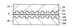
光ディスク1は、図2に示すように、2枚のディスク1A、1Bを貼り合わせた構造とされている。すなわち、図2は、光ディスク1の断面構造を示すものである。厚さ0.6mmの基板2Aに、例えばアルミニュームの第1の反射膜3Aが積層され、これに保護膜4Aが積層され、ディスク1Aが形成される。また、厚さ0.6mmの基板2Bに、例えばアルミニュームの第2の反射膜3Bが積層され、これに保護膜4Bが積層され、光ディスク1Bが形成される。これら2枚のディスク1AとディスクBへとが、接着層5を介して貼り合わされる。
【0013】
図1において、光ディスク1のエリアA1にデータが記録される。そして、データ記録エリアA1の内周側の、データ記録に用いられないエリアA2に、ディスクの情報を記憶させるための回路部6と、回路部6から導出されたコイル部7とが配設される。コイル部7は、光ディスク1と同一の中心軸となるように埋設される。
【0014】
前述したように、光ディスク1は、2枚のディスク1A及び1Bを貼り合わせた構成とされており、回路部6及びコイル部7は、この2枚のディスク1AとディスクBとの間に配置される。すなわち、図3に示すように、ディスク1Aの回路部6及びコイル部7が配置される部分には、凹部8Aが形成され、同様に、光ディスク1Bの回路部6及びコイル部7が配置される部分には、凹部8Bが形成される。ディスク1A及び1Bを貼り合わせたときに、凹部8Aと凹部8Bとの間に形成される間隙に、回路部6及びコイル部7が配置される。このように、回路部6及びコイル部7は、2枚のディスク1A及び1Bとの間に埋め込まれているため、回路部6及びコイル部7を配置しても、ディスクの物理的な形状は変わらない。
【0015】
図4は、回路部6の構成を示すものである。図4において、メモリ12に、ファイルや番組の内容、記録年月日、履歴、ID等が記憶される。このメモリ12に対するデータの読出し/書込みは、CPU11により制御される。外部とのデータの入出力は、コイル部7及び送受信回路13により、電磁波により非接触で行われる。また、外部から与えられる搬送波を平滑して、電源が形成される。形成された電源は、電源回路14から、CPU11、メモリ12、送受信回路13に供給される。
【0016】
図5は、光ディスク1内の回路部6との間で、データの授受を行うための外部回路の構成を示すものである。図5において、CPU21に対して、メモリ22と、キーボード23と、送受信回路24が設けられる。送受信回路24からは、コイル部25が導出される。データの入出力は、コイル部25及び送受信回路14により行われる。送受信回路14に対して、電源回路26が設けられている。
【0017】
図4に示した光ディスク1内の回路部6と、図5に示した外部の回路との間のデータの入出力は、図6に示すようにして行われる。図6に示すように、光ディスク1のコイル部7と外部の回路のコイル部25とは、対向して配置される。前述したように、光ディスク1のコイル部7は、光ディスク1の回転軸と同じ回転軸上に配設されている。外部のコイル部25も、光ディスク1の回転軸と同じ回転軸上に配置される。このように、コイル部7とコイル部25とを対向して配置すると、コイル部7とコイル部25とは結合する。
【0018】
外部の回路から光ディスク1内の回路部6にデータを送る場合には、CPU21からのデータが送受信回路24に送られる。送受信回路24でデータが変調される。この変調されたデータは、コイル部25に供給される。コイル部25とコイル部7とは結合されているため、このコイル部25の出力は、コイル部7に伝達され、コイル部7の出力が送受信回路13に供給される。送受信回路13で、このデータが復調されると共に、送られてきたデータの搬送波が整流され、電源が形成される。この電源は、CPU11、メモリ12、送受信回路13に供給される。送受信回路13で復調されたデータは、CPU11の制御の基に、メモリ12に記憶される。
【0019】
光ディスク1内の回路部6から外部の回路にデータを出力する場合には、CPU11の制御の基に、メモリ12からのデータが読み出される。このデータは、送受信回路13に供給される。送受信回路13で、このデータが変調される。送受信回路13の出力がコイル部7に供給される。コイル部7とコイル部25とは結合されているため、このコイル部7の出力は、コイル部25に伝達され、コイル部25の出力が送受信回路24に供給される。送受信回路24で、送られてきたデータが復調される。復調されたデータは、送受信回路24からCPU21に送られる。
【0020】
このように、この発明が適用された光ディスクでは、光ディスク1の内部に、CPU11、メモリ12、送受信回路13、電源回路14からなる回路部6と、コイル部7とが埋め込まれる。そして、外部の回路との間で、非接触でデータの入出力を行うことができる。回路部6及びコイル部7が光ディスク1内に埋め込まれているので、ディスクの外形は変化せず、互換性が保てる。また、外部との間のデータの入出力を非接触で行なえるので、信頼性が向上される。
【0021】
なお、上述の例では、ディスクの内周側のエリアA2に回路部6とコイル部7とを配設しているが、ディスクの外周側のエリアA3に回路部6及びコイル部7を配設するようにしても良い。
【0022】
【発明の効果】
この発明によれば、光ディスクが2枚のディスクを貼り合わせて形成され、この2枚のディスクの間に、CPU、メモリ、送受信回路、電源回路からなる回路部と、回路部から導出されたコイル部とが埋め込まれる。回路部及びコイル部がディスク内に埋め込まれているので、ディスクの外形は変化せず、互換性が保てる。また、光ディスクに埋め込まれたコイル部と外部の回路のコイル部とが対向して配置され、結合される。このため、光ディスクの内部の回路部と、外部の回路部との間で、非接触でデータの入出力を行うことができる。そして、光ディスクに埋め込まれたコイル部は、その回転軸がディスクの回転軸と同一であるため、ディスクが回転している間でも、外部の回路のコイル部との間の結合状態が安定に保たれる。
【図面の簡単な説明】
【図1】この発明が適用された光ディスクの説明に用いる平面図である。
【図2】この発明が適用された光ディスクの説明に用いる断面図である。
【図3】この発明が適用された光ディスクの説明に用いる断面図である。
【図4】この発明が適用された光ディスクの説明に用いるブロック図である。
【図5】この発明が適用された光ディスクの説明に用いるブロック図である。
【図6】この発明が適用された光ディスクの説明に用いるブロック図である。
【符号の説明】
1・・・光ディスク,1A,1B・・・ディスク,6・・・回路部,7・・・コイル部[0001]
BACKGROUND OF THE INVENTION
The present invention relates to an optical disc capable of recording the contents and history of the disc, and more particularly to an optical disc suitable for use in a DVD.
[0002]
[Prior art]
An optical disc (referred to as a DVD) having a recording capacity of about 8 to 10 Gbytes, which is several times that of a current compact disc, by using a laser beam having a short wavelength and increasing the numerical aperture of an objective lens. Has been developed. Such a DVD is expected to be used not only for recording a digital video signal compressed by MPEG2, for example, for reproducing moving images, but also as a recording medium for recording large-capacity digital data.
[0003]
In a large-capacity recording medium such as a DVD, the amount of data to be recorded becomes enormous, making it difficult to manage the data. In addition, since a digital video signal is recorded on a DVD, it is necessary to manage the history of recorded program contents, recording date, number of times of recording, etc., and management of ID information such as the presence or absence of protection. . Therefore, it is conceivable to provide a memory for storing information relating to the disk, and record the contents of the disk file, program, recording date, history, ID, and the like.
[0004]
As described above, when a memory for storing information related to a disk is provided, it is conceivable to provide a memory in which information on the disk is recorded in a disk cartridge in which the disk is stored. In this case, when the disc is loaded in the player main body, the memory in the disc cartridge and the controller in the player main body are connected via the connector. Information relating to the disk such as file and program contents, recording date, history, ID, and the like is read from the memory in the disk cartridge, thereby managing the disk.
[0005]
[Problems to be solved by the invention]
However, the DVD does not have a structure in which the disk and the disk cartridge are integrated in order to achieve compatibility with the current compact disk. For this reason, as described above, a configuration in which a memory is provided in the disk cartridge cannot be adopted.
[0006]
Therefore, it is conceivable to install a memory for storing disk information in the disk so as to cope with the case of an optical disk having no disk cartridge. However, in this case, since the disc is rotating, the memory attached to the disc and the controller in the player main body cannot be connected with a connector. It is conceivable that a signal line led out from the memory side in the disk is annularly arranged along the circumference of the disk and a brush is slid on the annular signal line. There is a problem with reliability in the structure.
[0007]
Therefore, for example, it is conceivable to connect the memory in the disc and the controller in the player body with electromagnetic waves. However, since such a function is provided in the disc, if the thickness of the disc and the shape of the disc are changed from those of the conventional disc, there is a problem in compatibility.
[0008]
Accordingly, an object of the present invention is to provide an optical disc capable of storing disc information in the disc without losing compatibility of the disc.
[0009]
[Means for Solving the Problems]
The present invention relates to an optical disc having a first signal recording surface and a second signal recording surface, wherein the first signal recording surface and the second signal recording surface are bonded together.
Apredetermined groove is provided on the first signal recording surfaceso as to surround the center hole of thedisc, a predetermined groove is provided ata position corresponding to the position of the groove on the second signal recording surface, and the first signal recording surface A memory in which information relatedto the disk is recorded ina gap formed by the grooves when the second signal recording surface is bonded, and an input / output unit that inputs and outputs information without contact with the memory; An optical disc characterized in that the optical disc is arranged.
[0010]
A circuit unit including a CPU, a memory, a transmission / reception circuit, and a power supply circuit, and a coil unit derived from the circuit unit are embedded in the optical disk. And by coupling | bonding a coil part, input / output of data can be performed non-contactedly with the exterior. Since the circuit portion and the coil portion are embedded in the disk, the outer shape of the disk does not change and compatibility can be maintained. In addition, since data can be input / output to / from the outside without contact, reliability is improved.
[0011]
DETAILED DESCRIPTION OF THE INVENTION
Embodiments of the present invention will be described below with reference to the drawings. In FIG. 1,
[0012]
As shown in FIG. 2, the
[0013]
In FIG. 1, data is recorded in an area A1 of the
[0014]
As described above, the
[0015]
FIG. 4 shows the configuration of the
[0016]
FIG. 5 shows a configuration of an external circuit for exchanging data with the
[0017]
Input / output of data between the
[0018]
When data is sent from an external circuit to the
[0019]
When data is output from the
[0020]
As described above, in the optical disk to which the present invention is applied, the
[0021]
In the above example, the
[0022]
【The invention's effect】
According to the present invention, an optical disc is formed by bonding two discs, a circuit unit including a CPU, a memory, a transmission / reception circuit, and a power supply circuit between the two discs, and a coil derived from the circuit unit The part is embedded. Since the circuit portion and the coil portion are embedded in the disk, the outer shape of the disk does not change and compatibility can be maintained. In addition, the coil portion embedded in the optical disk and the coil portion of the external circuit are arranged to face each other and coupled. Therefore, it is possible to input / output data without contact between a circuit unit inside the optical disc and an external circuit unit. The coil portion embedded in the optical disk has the same rotation axis as that of the disk, so that the coupling state with the coil portion of the external circuit is stably maintained even while the disk is rotating. Be drunk.
[Brief description of the drawings]
FIG. 1 is a plan view used for explaining an optical disc to which the present invention is applied.
FIG. 2 is a cross-sectional view used for explaining an optical disc to which the present invention is applied.
FIG. 3 is a cross-sectional view used for explaining an optical disc to which the present invention is applied.
FIG. 4 is a block diagram used for explaining an optical disc to which the present invention is applied.
FIG. 5 is a block diagram used to describe an optical disc to which the present invention is applied.
FIG. 6 is a block diagram used to describe an optical disc to which the present invention is applied.
[Explanation of symbols]
DESCRIPTION OF
Claims (3)
Translated fromJapanese上記第1の信号記録面において上記ディスクの中心孔を包囲するように所定の溝を設け、上記第2の信号記録面において上記溝の位置に対応する位置に所定の溝を設け、上記第1の信号記録面と上記第2の信号記録面とを貼り合わせたときに上記溝同士によって形成される間隙に、上記ディスクに関わる情報が記録されたメモリと、上記メモリに対して非接触で情報の入出力を行う入出力部とを配設するようにしたことを特徴とする光ディスク。In an optical disc having a first signal recording surface and a second signal recording surface, wherein the first signal recording surface and the second signal recording surface are bonded together,
Apredetermined groove is provided on the first signal recording surfaceso as to surround the center hole of the disc, and a predetermined groove is provided ata position corresponding to the position of the groove on the second signal recording surface.And a memory in which information relating to the disc is recorded ina gap formed by the grooves when the signal recording surface of the second signal recording surface and the second signal recording surface are bonded together, and information without contact with the memory An optical disc characterized by comprising an input / output unit for performing input / output of.
Priority Applications (1)
| Application Number | Priority Date | Filing Date | Title |
|---|---|---|---|
| JP07320596AJP3882218B2 (en) | 1996-03-04 | 1996-03-04 | optical disk |
Applications Claiming Priority (1)
| Application Number | Priority Date | Filing Date | Title |
|---|---|---|---|
| JP07320596AJP3882218B2 (en) | 1996-03-04 | 1996-03-04 | optical disk |
Publications (2)
| Publication Number | Publication Date |
|---|---|
| JPH09245381A JPH09245381A (en) | 1997-09-19 |
| JP3882218B2true JP3882218B2 (en) | 2007-02-14 |
Family
ID=13511427
Family Applications (1)
| Application Number | Title | Priority Date | Filing Date |
|---|---|---|---|
| JP07320596AExpired - Fee RelatedJP3882218B2 (en) | 1996-03-04 | 1996-03-04 | optical disk |
Country Status (1)
| Country | Link |
|---|---|
| JP (1) | JP3882218B2 (en) |
Families Citing this family (65)
| Publication number | Priority date | Publication date | Assignee | Title |
|---|---|---|---|---|
| JP3895830B2 (en)* | 1997-06-18 | 2007-03-22 | インテリジェントディスク株式会社 | Storage medium having electronic circuit |
| JPH1116206A (en)* | 1997-06-19 | 1999-01-22 | Oputoromu:Kk | Storage medium with electronic circuit and its manufacture |
| JP2000215456A (en)* | 1999-01-18 | 2000-08-04 | Hitachi Ltd | Disc, recording / reproducing apparatus, and recording / reproducing method |
| CN1833279B (en) | 2003-05-30 | 2010-11-03 | 松下电器产业株式会社 | Optical disc |
| US7519328B2 (en) | 2006-01-19 | 2009-04-14 | Murata Manufacturing Co., Ltd. | Wireless IC device and component for wireless IC device |
| JP2007253372A (en)* | 2006-03-22 | 2007-10-04 | Meiki Co Ltd | Mold for molding disk substrate, method for producing disk, and disk |
| DE112007000799B4 (en) | 2006-04-10 | 2013-10-10 | Murata Mfg. Co., Ltd. | Wireless IC device |
| JP4135770B2 (en) | 2006-04-14 | 2008-08-20 | 株式会社村田製作所 | antenna |
| EP2009736B1 (en) | 2006-04-14 | 2016-01-13 | Murata Manufacturing Co. Ltd. | Wireless ic device |
| US9064198B2 (en) | 2006-04-26 | 2015-06-23 | Murata Manufacturing Co., Ltd. | Electromagnetic-coupling-module-attached article |
| JP4803253B2 (en) | 2006-04-26 | 2011-10-26 | 株式会社村田製作所 | Article with power supply circuit board |
| WO2007138919A1 (en) | 2006-05-26 | 2007-12-06 | Murata Manufacturing Co., Ltd. | Data coupler |
| EP2023275B1 (en) | 2006-06-01 | 2011-04-27 | Murata Manufacturing Co. Ltd. | Radio frequency ic device and composite component for radio frequency ic device |
| WO2007145053A1 (en) | 2006-06-12 | 2007-12-21 | Murata Manufacturing Co., Ltd. | Electromagnetically coupled module, wireless ic device inspecting system, electromagnetically coupled module using the wireless ic device inspecting system, and wireless ic device manufacturing method |
| CN101467209B (en) | 2006-06-30 | 2012-03-21 | 株式会社村田制作所 | Optical disc |
| JP4957724B2 (en) | 2006-07-11 | 2012-06-20 | 株式会社村田製作所 | Antenna and wireless IC device |
| WO2008023636A1 (en) | 2006-08-24 | 2008-02-28 | Murata Manufacturing Co., Ltd. | Wireless ic device inspecting system and wireless ic device manufacturing method using the same |
| US7886315B2 (en) | 2007-01-30 | 2011-02-08 | Sony Corporation | Optical disc case, optical disc tray, card member, and manufacturing method |
| US8009101B2 (en) | 2007-04-06 | 2011-08-30 | Murata Manufacturing Co., Ltd. | Wireless IC device |
| US7762472B2 (en) | 2007-07-04 | 2010-07-27 | Murata Manufacturing Co., Ltd | Wireless IC device |
| US8235299B2 (en) | 2007-07-04 | 2012-08-07 | Murata Manufacturing Co., Ltd. | Wireless IC device and component for wireless IC device |
| EP2166617B1 (en) | 2007-07-09 | 2015-09-30 | Murata Manufacturing Co. Ltd. | Wireless ic device |
| CN102915462B (en) | 2007-07-18 | 2017-03-01 | 株式会社村田制作所 | Wireless IC device |
| US7830311B2 (en) | 2007-07-18 | 2010-11-09 | Murata Manufacturing Co., Ltd. | Wireless IC device and electronic device |
| JP2009080761A (en) | 2007-09-27 | 2009-04-16 | Sony Corp | Information reader, and information reading method |
| JP4462388B2 (en) | 2007-12-20 | 2010-05-12 | 株式会社村田製作所 | Wireless IC device |
| CN103500875B (en) | 2007-12-26 | 2015-12-02 | 株式会社村田制作所 | Antenna assembly and Wireless IC device |
| EP2284949B1 (en) | 2008-05-21 | 2016-08-03 | Murata Manufacturing Co. Ltd. | Wireless ic device |
| WO2009145007A1 (en) | 2008-05-26 | 2009-12-03 | 株式会社村田製作所 | Wireless ic device system and method for authenticating wireless ic device |
| JP4557186B2 (en) | 2008-06-25 | 2010-10-06 | 株式会社村田製作所 | Wireless IC device and manufacturing method thereof |
| WO2010001987A1 (en) | 2008-07-04 | 2010-01-07 | 株式会社村田製作所 | Wireless ic device |
| EP2320519B1 (en) | 2008-08-19 | 2017-04-12 | Murata Manufacturing Co., Ltd. | Wireless ic device and method for manufacturing same |
| JP5429182B2 (en) | 2008-10-24 | 2014-02-26 | 株式会社村田製作所 | Wireless IC device |
| JP4605318B2 (en) | 2008-11-17 | 2011-01-05 | 株式会社村田製作所 | Antenna and wireless IC device |
| EP2385580B1 (en) | 2009-01-30 | 2014-04-09 | Murata Manufacturing Co., Ltd. | Antenna and wireless ic device |
| JP5510450B2 (en) | 2009-04-14 | 2014-06-04 | 株式会社村田製作所 | Wireless IC device |
| EP2568534A3 (en) | 2009-04-21 | 2014-05-14 | Murata Manufacturing Co., Ltd. | Antenna devie and method of setting resonant frequency of antenna device |
| WO2011001709A1 (en) | 2009-07-03 | 2011-01-06 | 株式会社村田製作所 | Antenna and antenna module |
| JP5201270B2 (en) | 2009-09-30 | 2013-06-05 | 株式会社村田製作所 | Circuit board and manufacturing method thereof |
| JP5304580B2 (en) | 2009-10-02 | 2013-10-02 | 株式会社村田製作所 | Wireless IC device |
| CN102576939B (en) | 2009-10-16 | 2015-11-25 | 株式会社村田制作所 | Antenna and wireless ic device |
| JP5418600B2 (en) | 2009-10-27 | 2014-02-19 | 株式会社村田製作所 | Transceiver and RFID tag reader |
| WO2011055702A1 (en) | 2009-11-04 | 2011-05-12 | 株式会社村田製作所 | Wireless ic tag, reader/writer, and information processing system |
| JP5327334B2 (en) | 2009-11-04 | 2013-10-30 | 株式会社村田製作所 | Communication terminal and information processing system |
| WO2011055701A1 (en) | 2009-11-04 | 2011-05-12 | 株式会社村田製作所 | Communication terminal and information processing system |
| WO2011108340A1 (en) | 2010-03-03 | 2011-09-09 | 株式会社村田製作所 | Wireless communication module and wireless communication device |
| JP5370581B2 (en) | 2010-03-24 | 2013-12-18 | 株式会社村田製作所 | RFID system |
| WO2011122163A1 (en) | 2010-03-31 | 2011-10-06 | 株式会社村田製作所 | Antenna and wireless communication device |
| JP5299351B2 (en) | 2010-05-14 | 2013-09-25 | 株式会社村田製作所 | Wireless IC device |
| JP5170156B2 (en) | 2010-05-14 | 2013-03-27 | 株式会社村田製作所 | Wireless IC device |
| GB2537773A (en) | 2010-07-28 | 2016-10-26 | Murata Manufacturing Co | Antenna apparatus and communication terminal instrument |
| JP5423897B2 (en) | 2010-08-10 | 2014-02-19 | 株式会社村田製作所 | Printed wiring board and wireless communication system |
| JP5630506B2 (en) | 2010-09-30 | 2014-11-26 | 株式会社村田製作所 | Wireless IC device |
| WO2012050037A1 (en) | 2010-10-12 | 2012-04-19 | 株式会社村田製作所 | Antenna apparatus and communication terminal apparatus |
| CN102971909B (en) | 2010-10-21 | 2014-10-15 | 株式会社村田制作所 | Communication terminal device |
| WO2012093541A1 (en) | 2011-01-05 | 2012-07-12 | 株式会社村田製作所 | Wireless communication device |
| CN103299325B (en) | 2011-01-14 | 2016-03-02 | 株式会社村田制作所 | RFID chip packaging and RFID tags |
| CN103119786B (en) | 2011-02-28 | 2015-07-22 | 株式会社村田制作所 | Wireless communication device |
| WO2012137717A1 (en) | 2011-04-05 | 2012-10-11 | 株式会社村田製作所 | Wireless communication device |
| WO2012157596A1 (en) | 2011-05-16 | 2012-11-22 | 株式会社村田製作所 | Wireless ic device |
| KR101338173B1 (en) | 2011-07-14 | 2013-12-06 | 가부시키가이샤 무라타 세이사쿠쇼 | Wireless communication device |
| WO2013035821A1 (en) | 2011-09-09 | 2013-03-14 | 株式会社村田製作所 | Antenna device and wireless device |
| JP5344108B1 (en) | 2011-12-01 | 2013-11-20 | 株式会社村田製作所 | Wireless IC device and manufacturing method thereof |
| JP5464307B2 (en) | 2012-02-24 | 2014-04-09 | 株式会社村田製作所 | ANTENNA DEVICE AND WIRELESS COMMUNICATION DEVICE |
| CN104487985B (en) | 2012-04-13 | 2020-06-26 | 株式会社村田制作所 | RFID tag inspection method and inspection device |
- 1996
- 1996-03-04JPJP07320596Apatent/JP3882218B2/ennot_activeExpired - Fee Related
Also Published As
| Publication number | Publication date |
|---|---|
| JPH09245381A (en) | 1997-09-19 |
Similar Documents
| Publication | Publication Date | Title |
|---|---|---|
| JP3882218B2 (en) | optical disk | |
| KR100309587B1 (en) | Information recording disk | |
| JP2000132871A (en) | Disc and recording / reproducing apparatus using the same | |
| EP0933760A2 (en) | Two-sided graphical image DVDs and methods for making same | |
| JPH04265567A (en) | Apparatus and method for identifying type of medium | |
| JPH08161790A (en) | Optical disc and optical disc device using the same | |
| US20050052985A1 (en) | Optical disc | |
| JPH0362381A (en) | Optical disk cartridge with flexible recording medium | |
| JPH10208297A (en) | Optical disk substrate | |
| JP3371840B2 (en) | Optical disk drive | |
| JPH06309840A (en) | Thereof optical disk and reproducing equipment of record | |
| JP2005071575A (en) | optical disk | |
| JP3077385B2 (en) | Cleaning disk and method of cleaning magneto-optical recording / reproducing device | |
| JP3478286B2 (en) | optical disk | |
| JP2005518622A (en) | Disk data storage medium having an edge tracking data surface | |
| JP2002092927A (en) | Optical pickup device, method for manufacturing optical element, optical information recording medium, and optical disk device | |
| JPH11185420A (en) | Cleaning equipment | |
| JP4073845B2 (en) | Optical recording medium | |
| JPS6323811Y2 (en) | ||
| JP2938906B2 (en) | Optical recording medium | |
| JPH11339421A (en) | Optical pickup cleaning device | |
| JPH05189809A (en) | Optical recording medium | |
| JPH04245081A (en) | Optical disk memory unit and information processing device | |
| JPH1097733A (en) | Optical information recording medium | |
| JP2005332469A (en) | Disk unit |
Legal Events
| Date | Code | Title | Description |
|---|---|---|---|
| A977 | Report on retrieval | Free format text:JAPANESE INTERMEDIATE CODE: A971007 Effective date:20050314 | |
| A131 | Notification of reasons for refusal | Free format text:JAPANESE INTERMEDIATE CODE: A131 Effective date:20050322 | |
| A521 | Request for written amendment filed | Free format text:JAPANESE INTERMEDIATE CODE: A523 Effective date:20050517 | |
| TRDD | Decision of grant or rejection written | ||
| A01 | Written decision to grant a patent or to grant a registration (utility model) | Free format text:JAPANESE INTERMEDIATE CODE: A01 Effective date:20061024 | |
| A61 | First payment of annual fees (during grant procedure) | Free format text:JAPANESE INTERMEDIATE CODE: A61 Effective date:20061106 | |
| FPAY | Renewal fee payment (event date is renewal date of database) | Free format text:PAYMENT UNTIL: 20091124 Year of fee payment:3 | |
| FPAY | Renewal fee payment (event date is renewal date of database) | Free format text:PAYMENT UNTIL: 20101124 Year of fee payment:4 | |
| FPAY | Renewal fee payment (event date is renewal date of database) | Free format text:PAYMENT UNTIL: 20101124 Year of fee payment:4 | |
| FPAY | Renewal fee payment (event date is renewal date of database) | Free format text:PAYMENT UNTIL: 20111124 Year of fee payment:5 | |
| LAPS | Cancellation because of no payment of annual fees |