JP3881973B2 - Method for forming silicon nitride film - Google Patents
Method for forming silicon nitride filmDownload PDFInfo
- Publication number
- JP3881973B2 JP3881973B2JP2003306306AJP2003306306AJP3881973B2JP 3881973 B2JP3881973 B2JP 3881973B2JP 2003306306 AJP2003306306 AJP 2003306306AJP 2003306306 AJP2003306306 AJP 2003306306AJP 3881973 B2JP3881973 B2JP 3881973B2
- Authority
- JP
- Japan
- Prior art keywords
- gas
- film
- flow rate
- supplied
- silicon nitride
- Prior art date
- Legal status (The legal status is an assumption and is not a legal conclusion. Google has not performed a legal analysis and makes no representation as to the accuracy of the status listed.)
- Expired - Fee Related
Links
- 229910052581Si3N4Inorganic materials0.000titleclaimsdescription46
- HQVNEWCFYHHQES-UHFFFAOYSA-Nsilicon nitrideChemical compoundN12[Si]34N5[Si]62N3[Si]51N64HQVNEWCFYHHQES-UHFFFAOYSA-N0.000titleclaimsdescription46
- 238000000034methodMethods0.000titleclaimsdescription13
- 239000007789gasSubstances0.000claimsdescription87
- IJGRMHOSHXDMSA-UHFFFAOYSA-NAtomic nitrogenChemical compoundN#NIJGRMHOSHXDMSA-UHFFFAOYSA-N0.000claimsdescription37
- BLRPTPMANUNPDV-UHFFFAOYSA-NSilaneChemical compound[SiH4]BLRPTPMANUNPDV-UHFFFAOYSA-N0.000claimsdescription34
- 229910000077silaneInorganic materials0.000claimsdescription34
- 239000000758substrateSubstances0.000claimsdescription31
- 230000015572biosynthetic processEffects0.000claimsdescription23
- 229910001873dinitrogenInorganic materials0.000claimsdescription21
- 238000005268plasma chemical vapour depositionMethods0.000claimsdescription11
- 238000009616inductively coupled plasmaMethods0.000claimsdescription10
- 239000011261inert gasSubstances0.000claimsdescription7
- 230000005284excitationEffects0.000claimsdescription4
- XUIMIQQOPSSXEZ-UHFFFAOYSA-NSiliconChemical compound[Si]XUIMIQQOPSSXEZ-UHFFFAOYSA-N0.000claims1
- 229910052710siliconInorganic materials0.000claims1
- 239000010703siliconSubstances0.000claims1
- QGZKDVFQNNGYKY-UHFFFAOYSA-NAmmoniaChemical compoundNQGZKDVFQNNGYKY-UHFFFAOYSA-N0.000description8
- 238000006243chemical reactionMethods0.000description8
- XKRFYHLGVUSROY-UHFFFAOYSA-NArgonChemical compound[Ar]XKRFYHLGVUSROY-UHFFFAOYSA-N0.000description6
- 238000005229chemical vapour depositionMethods0.000description5
- 230000001681protective effectEffects0.000description5
- 239000004065semiconductorSubstances0.000description5
- UFHFLCQGNIYNRP-UHFFFAOYSA-NHydrogenChemical compound[H][H]UFHFLCQGNIYNRP-UHFFFAOYSA-N0.000description4
- 229910021529ammoniaInorganic materials0.000description4
- 238000010586diagramMethods0.000description4
- 239000001307heliumSubstances0.000description4
- 229910052734heliumInorganic materials0.000description4
- SWQJXJOGLNCZEY-UHFFFAOYSA-Nhelium atomChemical compound[He]SWQJXJOGLNCZEY-UHFFFAOYSA-N0.000description4
- 239000001257hydrogenSubstances0.000description4
- 229910052739hydrogenInorganic materials0.000description4
- 229910007991Si-NInorganic materials0.000description3
- 229910006294Si—NInorganic materials0.000description3
- 229910052786argonInorganic materials0.000description3
- 238000000354decomposition reactionMethods0.000description3
- 238000000151depositionMethods0.000description3
- 230000008021depositionEffects0.000description3
- 239000002994raw materialSubstances0.000description3
- 238000005033Fourier transform infrared spectroscopyMethods0.000description2
- 238000004566IR spectroscopyMethods0.000description2
- 230000007935neutral effectEffects0.000description2
- 239000002245particleSubstances0.000description2
- XAGFODPZIPBFFR-UHFFFAOYSA-NaluminiumChemical compound[Al]XAGFODPZIPBFFR-UHFFFAOYSA-N0.000description1
- 229910052782aluminiumInorganic materials0.000description1
- 238000007796conventional methodMethods0.000description1
- 230000000694effectsEffects0.000description1
- 238000004519manufacturing processMethods0.000description1
- 239000000463materialSubstances0.000description1
- 229910052757nitrogenInorganic materials0.000description1
Images


Landscapes
- Chemical Vapour Deposition (AREA)
- Formation Of Insulating Films (AREA)
Description
Translated fromJapanese本発明は、窒化シリコン膜の成膜方法に関し、低温の処理温度であっても良好な膜質で且つ低ストレスな窒化シリコン膜が成膜できるように工夫したものである。 The present invention relates to a method for forming a silicon nitride film, which is devised so that a silicon nitride film having good film quality and low stress can be formed even at a low processing temperature.
現在、半導体の製造では、プラズマCVD(Chemical Vapor Deposition)装置を用いた成膜が知られている。誘導結合プラズマ(inductively coupled plasma;ICP)型のプラズマCVD装置は、膜の材料となる原料ガスを容器内の成膜室の中に導入し、高周波アンテナにRF電流(高周波電流)を流して、成膜室内に高周波の電磁波を入射してプラズマ状態にし、プラズマ中の活性粒子(励起原子または励起分子)によって基板表面の化学的な反応を促進して成膜を行う装置である。 At present, in semiconductor manufacturing, film formation using a plasma CVD (Chemical Vapor Deposition) apparatus is known. An inductively coupled plasma (ICP) type plasma CVD apparatus introduces a raw material gas as a film material into a film forming chamber in a container, and causes an RF current (high frequency current) to flow through a high frequency antenna. In this apparatus, a high frequency electromagnetic wave is incident into a film forming chamber to form a plasma state, and a chemical reaction on the substrate surface is promoted by active particles (excited atoms or excited molecules) in the plasma to form a film.
半導体素子(例えばDRAM)では、素子保護用膜として窒化シリコン(SiN)を用いることがあり、この窒化シリコン(SiN)は、ICP型のプラズマCVD装置により成膜される。 In a semiconductor element (for example, DRAM), silicon nitride (SiN) may be used as an element protection film, and this silicon nitride (SiN) is formed by an ICP type plasma CVD apparatus.
窒化シリコンSiNを成膜するには、従来では、ICP型のプラズマCVD装置内に、原料ガスとしてアンモニア(NH3)とシラン(SiH4)を成膜室内に供給しつつ、基板温度を350°C以上にして、RFパワーを6W/sccm以上としていた。
半導体素子の保護用膜として窒化シリコン(SiN)を成膜するために、原料ガスとしてアンモニア(NH3)を用いた場合には、原料であるアンモニア(NH3)中に水素が含まれているため、成膜された保護用膜の膜中の水素含有率が多くなってしまい、保護用膜としての品質が低下していた。When ammonia (NH3 ) is used as a source gas for forming silicon nitride (SiN) as a protective film for a semiconductor element, hydrogen is contained in the source ammonia (NH3 ). For this reason, the hydrogen content in the formed protective film is increased, and the quality as the protective film is lowered.
また最近では、集積度の高いDRAMや、MRAMや、FeRAMなどが開発されてきたが、これら高集積度DRAMやMRAMやFeRAMは熱に弱いため、処理温度が300°C以下になるように要求されるようになってきている。このため、保護用膜を成膜するのに、低温(300°C以下)で処理する必要がでてきたが、従来の手法では、かかる低温では良質な膜質を得ることができなかった。 Recently, highly integrated DRAM, MRAM, FeRAM, and the like have been developed, but these highly integrated DRAM, MRAM, and FeRAM are vulnerable to heat, so that the processing temperature is required to be 300 ° C. or lower. It has come to be. For this reason, in order to form a protective film, it has been necessary to perform the treatment at a low temperature (300 ° C. or lower), but the conventional method cannot obtain a good film quality at such a low temperature.
本発明は、上記従来技術に鑑み、膜質が良好で、しかも、低温での処理で膜成形ができる窒化シリコン膜の成膜方法を提供することを目的とする。 An object of the present invention is to provide a method for forming a silicon nitride film which has good film quality and can be formed by low-temperature processing in view of the above prior art.
上記課題を解決する本発明の構成は、誘導結合プラズマ型のプラズマCVD装置を用いて、成膜室内の基板上に窒化シリコン膜を成膜する成膜方法であって、
前記成膜室に供給する原料ガスとしてシランガスと窒素ガスを用い、
シランガスの供給流量に対して、窒素ガスの供給流量を10倍以上とし、ガスの総供給量に対する高周波パワーを3W/sccm以上とし、基板温度を50°C〜300°Cとし、
更に、前記成膜室のうちで入射される電磁波が強い空間領域に前記窒素ガスを供給し、前記成膜室内に設置した基板の近傍の空間領域に前記シランガスを供給することを特徴とする。The structure of the present invention that solves the above problem is a film forming method for forming a silicon nitride film on a substrate in a film forming chamber using an inductively coupled plasma type plasma CVD apparatus,
Silane gas and nitrogen gas are used as source gases to be supplied to the film formation chamber,
The supply flow rate of nitrogen gas is 10 times or more than the supply flow rate of silane gas, the high frequency power for the total supply amount of gas is 3 W / sccm or more, the substrate temperature is 50 ° C. to 300 ° C.,
Further, the nitrogen gas is supplied to a space region where the incident electromagnetic wave is strong in the film formation chamber, and the silane gas is supplied to a space region in the vicinity of the substrate installed in the film formation chamber .
また本発明の構成は、誘導結合プラズマ型のプラズマCVD装置を用いて、成膜室内の基板上に窒化シリコン膜を成膜する成膜方法であって、
前記成膜室に供給する原料ガスとしてシランガスと窒素ガスを用い、
シランガスの供給流量に対して、窒素ガスの供給流量を10倍以上とし、ガスの総供給量に対する高周波パワーを3W/sccm以上とし、基板温度を50°C〜300°Cとし、
更に、前記成膜室のうちで入射される電磁波が強い空間領域に前記窒素ガスを供給し、前記成膜室内に設置した基板の近傍の空間領域に前記シランガスを供給し、
更に、成膜圧力を10mTorr〜50mTorrとしたことを特徴とする。According to another aspect of the present invention, there is provided a film forming method for forming a silicon nitride film on a substrate in a film forming chamber using aninductively coupled plasma type plasma CVD apparatus,
Silane gas and nitrogen gas are used as source gases to be supplied to the film formation chamber,
The supply flow rate of nitrogen gas is 10 times or more than the supply flow rate of silane gas, the high frequency power for the total supply amount of gas is 3 W / sccm or more, the substrate temperature is 50 ° C. to 300 ° C.,
Furthermore, the nitrogen gas is supplied to a space region where the incident electromagnetic wave is strong in the film formation chamber, and the silane gas is supplied to a space region in the vicinity of the substrate installed in the film formation chamber,
Further, the film forming pressure is set to 10 mTorr to 50 mTorr.
また本発明の構成は、上記成膜方法において、励起ガスとしての不活性ガスを、シランガスと窒素ガスの総供給流量の20%以下の流量で、前記成膜室内に供給することを特徴とする。 Further, the structure of the present invention is characterized in that, in the film forming method, an inert gas as an excitation gas is supplied into the film forming chamber at a flow rate of 20% or less of a total supply flow rate of silane gas and nitrogen gas. .
本発明によれば、低温な処理温度であっても、良好な膜質で低ストレスな窒化シリコン膜を、迅速に(成膜速度を速くして)成膜することができる。 According to the present invention, a silicon nitride film having good film quality and low stress can be formed quickly (by increasing the film forming speed) even at a low processing temperature.
本発明の窒化シリコン膜の成膜方法では、ICP型のプラズマCVD装置を用いて、シラン(SiH4)ガスと窒素(N2)ガスを原料ガスとして、次のような成膜条件で窒化シリコン(SiN)を成膜する。In the silicon nitride film forming method of the present invention, silicon nitride is used under the following film forming conditions by using an ICP type plasma CVD apparatus, using silane (SiH4 ) gas and nitrogen (N2 ) gas as source gases. (SiN) is deposited.
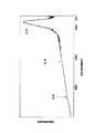
(1)シラン(SiH4)ガスの供給流量に対して、窒素(N2)ガスの供給流量を10倍以上とし、ガスの総供給量に対する高周波パワー(RFパワー:成膜室に入射する電磁波のエネルギー)を3W/sccm以上とし、基板温度を50°C〜300°Cとする。これにより、図1に例示する良好な膜質の窒化シリコン(SiN)膜を成膜することができる。同図は、成膜温度が200℃、シランガス流量に対する窒素ガス流量の比(N2/SiH4)が20倍にてSi−H結合が検知されていないFTIR(赤外分光)特性図である。(1) The supply flow rate of nitrogen (N2 ) gas is at least 10 times the supply flow rate of silane (SiH4 ) gas, and the high frequency power (RF power: electromagnetic waves incident on the film formation chamber) with respect to the total supply amount of gas Energy) is 3 W / sccm or more, and the substrate temperature is 50 ° C. to 300 ° C. Thereby, a silicon nitride (SiN) film having a good film quality illustrated in FIG. 1 can be formed. This figure is an FTIR (infrared spectroscopy) characteristic diagram in which the film forming temperature is 200 ° C., the ratio of the nitrogen gas flow rate to the silane gas flow rate (N2 / SiH4 ) is 20 times, and no Si—H bond is detected. .
(2)上記(1)の成膜条件に加えて、成膜圧力を10mTorr〜50mTorrとする。これにより、後述するように、低ストレスな窒化シリコン(SiN)膜を成膜することができる。(2) In addition to the film forming conditions of (1) above, the film forming pressure is set to 10 mTorr to 50 mTorr. As a result, a low-stress silicon nitride (SiN) film can be formed as will be described later.
(3)上記(1)の成膜条件に加えて、または上記(1),(2)の成膜条件に加えて、CVD装置の成膜室のうちで入射される電磁波が強い空間領域に窒素(N2)ガスを供給し、CVD装置の成膜室に設置した基板の近傍の空間領域にシラン(SiH4)ガスを供給する。これにより、後述するように、分解しにくい窒素(N2)ガスを効率良く分解することによりSi−N反応を促進し、膜質の改善を達成することができる。(3) In addition to the film forming conditions of (1) above or in addition to the film forming conditions of (1) and (2) above, in a space region where an incident electromagnetic wave is strong in the film forming chamber of the CVD apparatus. Nitrogen (N2 ) gas is supplied, and silane (SiH4 ) gas is supplied to a space region in the vicinity of the substrate installed in the film formation chamber of the CVD apparatus. Thereby, as will be described later, it is possible to promote the Si—N reaction by efficiently decomposing nitrogen (N2 ) gas, which is difficult to decompose, and to improve the film quality.
(4)上記(1)の成膜条件に加えて、または上記(1),(2)の成膜条件に加えて、または上記(1),(2),(3)の成膜条件に加えて、励起ガスとしてアルゴン(Ar)やヘリウム(He)などの不活性ガスを、シラン(SiH4)ガスと窒素(N2)ガスの総供給流量の20%以下の流量で供給する。これにより、後述するように、原料ガスの分解をアシストして、成膜速度を向上させることができる。(4) In addition to the film forming conditions of (1) above, or in addition to the film forming conditions of (1) and (2) above, or to the film forming conditions of (1), (2) and (3) above. In addition, an inert gas such as argon (Ar) or helium (He) is supplied as an excitation gas at a flow rate of 20% or less of the total supply flow rate of silane (SiH4 ) gas and nitrogen (N2 ) gas. Thereby, as will be described later, the decomposition of the source gas can be assisted to improve the film formation rate.
ここで、本発明方法を実施するプラズマCVD装置を、図2を参照して説明する。 Here, a plasma CVD apparatus for carrying out the method of the present invention will be described with reference to FIG.
図2に示すように、基部1には円筒状のアルミニウム製の容器2が設けられ、容器2内に成膜室3が形成されている。容器2の上部には、電磁波を透過させる円形の天井板4が設けられ、容器2の中心における成膜室3にはウエハ支持台5が備えられている。ウエハ支持台5は半導体の基板6を静電的に吸着保持する円盤状の載置部7を有し、載置部7は支持軸8に支持されている。 As shown in FIG. 2, the
載置部7には、バイアス電源9および静電電源10が接続され、載置部7に低周波を発生させると共に静電気力を発生させる。ウエハ支持台5は全体が昇降自在もしくは支持軸8が伸縮自在とすることで、上下方向の高さが最適な高さに調整できるようになっている。 A bias power source 9 and an
天井板4の上には、例えば、円形リング状の高周波アンテナ11が配置され、高周波アンテナ11には整合器12を介して高周波電源13が接続されている。高周波アンテナ11に高周波電力を供給することにより電磁波が容器2の成膜室3に入射する。容器2内に入射された電磁波は、成膜質3内のガスをイオン化してプラズマを発生させる。 For example, a circular ring-shaped high-frequency antenna 11 is disposed on the
容器2には、シラン(SiH4)ガスを成膜室3内に供給するガス供給ノズル14と、窒素(N2)ガスを成膜室3内に供給するガス供給ノズル15と、不活性ガス(アルゴンArやヘリウムHe)を成膜室3内に供給するためのガス供給ノズル16が設けられている。The
本例では、ガス供給ノズル14〜15の、高さ方向に関する配置位置は、ガス供給ノズル15が最上段にあり、ガス供給ノズル16が中段にあり、ガス供給ノズル14が最下段にある。
これにより、ガス供給ノズル15を介して供給される窒素(N2)ガスが、成膜室3のうちで高周波アンテナ11から入射される電磁波が強い空間領域、即ち、プラズマがより強く発生する空間領域に供給される。
また、ガス供給ノズル14を介して供給されるシラン(SiH4)ガスが、成膜室3のうちで基板6近傍の空間領域に供給される。In this example, the
Thereby, the nitrogen (N2 ) gas supplied through the
Further, silane (SiH4 ) gas supplied via the
また基部1には容器2内を排気するための真空排気系(図示省略)に接続される排気口17が設けられている。また、図示は省略したが、容器2には基板6の搬入、搬出口が設けられ、図示しない搬送室との間で基板6が搬入・搬出される。 The
上述したICP型のプラズマCVD装置では、ウエハ支持台5の載置部7に基板6が載せられ、静電的に吸着される。そしてガス供給ノズル14〜16を介して、成膜室3内にシラン(SiH4)ガスと、窒素(N2)ガスと、不活性ガス(アルゴンArやヘリウムHe)が供給される。また、高周波電源13から高周波アンテナ11に電力を供給して高周波の電磁波を発生させると共にバイアス電源9から載置部7に低周波電力を供給する。
このとき成膜条件を上述した(1)〜(4)とする。In the above-described ICP type plasma CVD apparatus, the
At this time, the film forming conditions are the above-described (1) to (4).
これにより、成膜室3内の原料ガスが放電して一部がプラズマ状態となる。このプラズマは、原料ガス中の他の中性分子に衝突して更に中性分子を電離、あるいは励起する。こうして生じた活性な粒子は、基板6の表面に吸着して効率良く化学反応を起こし、堆積して、基板6上に、良好な膜質で低ストレスな窒化シリコン(SiN)膜を成膜することができる。 As a result, the raw material gas in the film forming chamber 3 is discharged and a part thereof is in a plasma state. This plasma collides with other neutral molecules in the source gas and further ionizes or excites the neutral molecules. The active particles thus generated are adsorbed on the surface of the
実施例1では、シラン(SiH4)ガスの供給流量に対して、窒素(N2)ガスの供給流量を10倍以上とし、ガスの総供給量に対する高周波パワー(RFパワー:成膜室に入射する電磁波のエネルギー)を3W/sccm以上とし、基板温度を50°C〜300°Cとした。In Example 1, the supply flow rate of nitrogen (N2 ) gas is 10 times or more than the supply flow rate of silane (SiH4 ) gas, and high frequency power (RF power: incident on the film formation chamber) with respect to the total supply amount of gas. The energy of the electromagnetic wave to be generated) was 3 W / sccm or more, and the substrate temperature was 50 ° C. to 300 ° C.
このようにすることにより、良好な膜質の窒化シリコン(SiN)膜を成膜することができた。第一に水素を含むアンモニア(NH3)ガスを使用せず、窒素(N2)ガスを用いることにより水素量を減らしている。次に、Si3N4反応に必要なSiH4流量に対するN2流量は、通常1:1で十分であるが、N2流量をSiH4流量の10倍とすることによりSi−H結合を抑制することができており、この多量のSiH4+N2反応で必要な窒素(N2)ガスの分解を促進するために十分なRFパワー(3W/sccm以上)を印加することによりSiN反応を促進した結果、300°C以下の温度領域でも良好な膜質を得ることができたのである。By doing so, it was possible to form a silicon nitride (SiN) film having a good film quality. First, the amount of hydrogen is reduced by using nitrogen (N2 ) gas without using ammonia (NH3 ) gas containing hydrogen. Next, the N2 flow rate relative to the SiH4 flow rate required for the Si3 N4 reaction is usually 1: 1, but the Si—H bond is suppressed by making the N2 flow rate 10 times the SiH4 flow rate. The SiN reaction is promoted by applying sufficient RF power (3 W / sccm or more) to promote the decomposition of nitrogen (N2 ) gas necessary for this large amount of SiH4 + N2 reaction. As a result, good film quality could be obtained even in a temperature range of 300 ° C. or lower.
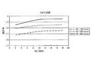
窒化シリコン(SiN)膜の膜質は、屈折率により判定することができ、屈折率が2.1に近いほど良好な膜質である。
図3は成膜温度(基板温度)を200°Cとしたときにおける、各RFパワーでの、屈折率と、シランガス流量に対する窒素ガス流量の比(N2/SiH4)との関係を示す特性図である。また図4は成膜温度(基板温度)を350°Cとしたときにおける、各RFパワーでの、屈折率と、シランガス流量に対する窒素ガス流量の比(N2/SiH4)との関係を示す特性である。
図4から分かるように、基板温度が350°C程度の高温で成膜をすると、流量やRFパワーに依存することなく、良好な膜質の窒化シリコン(SiN)膜の成膜ができる。
一方、図3から分かるように、基板温度が200°のような低温条件では、シランガス流量に対する窒素ガス流量の比(N2/SiH4)が10以上で、RFパワーを3W/sccm以上とすることにより、良好な膜質の窒化シリコン(SiN)膜の成膜ができることが判明した。The film quality of the silicon nitride (SiN) film can be determined by the refractive index. The closer the refractive index is to 2.1, the better the film quality.
FIG. 3 shows the relationship between the refractive index and the ratio of the nitrogen gas flow rate to the silane gas flow rate (N2 / SiH4 ) at each RF power when the film forming temperature (substrate temperature) is 200 ° C. FIG. FIG. 4 shows the relationship between the refractive index and the ratio of the nitrogen gas flow rate to the silane gas flow rate (N2 / SiH4 ) at each RF power when the film forming temperature (substrate temperature) is 350 ° C. It is a characteristic.
As can be seen from FIG. 4, when the film is formed at a high substrate temperature of about 350 ° C., a silicon nitride (SiN) film having a good film quality can be formed without depending on the flow rate or RF power.
On the other hand, as can be seen from FIG. 3, under a low temperature condition such as a substrate temperature of 200 °, the ratio of the nitrogen gas flow rate to the silane gas flow rate (N2 / SiH4 ) is 10 or more and the RF power is 3 W / sccm or more. Thus, it was found that a silicon nitride (SiN) film having a good film quality can be formed.
実施例2では、実施例1の成膜条件に加えて、成膜圧力を10mTorr〜50mTorrとした。これにより、低ストレスな窒化シリコン(SiN)膜を成膜することができた。窒化シリコン膜のストレス許容値は、250Mpaである。 In Example 2, in addition to the film forming conditions of Example 1, the film forming pressure was set to 10 mTorr to 50 mTorr. As a result, a low-stress silicon nitride (SiN) film could be formed. The allowable stress value of the silicon nitride film is 250 Mpa.
図5はSiN膜のストレスと成膜圧力との関係を示す。図5から分かるように、成膜圧力を10mTorr〜50mTorrとすれば、ストレスが250Mpa以下になることが判明した。この結果、良好な膜質を維持しつつ、さらに低ストレスな窒化シリコン(SiN)膜を成膜することができた。 FIG. 5 shows the relationship between the stress of the SiN film and the deposition pressure. As can be seen from FIG. 5, when the film forming pressure is 10 mTorr to 50 mTorr, the stress is found to be 250 Mpa or less. As a result, it was possible to form a silicon nitride (SiN) film with lower stress while maintaining good film quality.
実施例3では、実施例1,2に示す成膜条件で、図2に示すCVD装置を用いることにより、シラン(SiH4)ガスに対してガス供給量が10倍以上となっている窒素(N2)ガスを、成膜室3のうちで高周波アンテナ11から入射される電磁波が強い空間領域、即ち、プラズマがより強く発生する空間領域に供給する。このため多量で且つ分解しにくい
窒素(N2)ガスを効率良く分解することができる。
また、シラン(SiH4)ガスが基板6近傍の空間領域に供給されるため、基板6の近傍にてSi−N反応が行われる。
この両方の効果が相乗して、Si−N反応が促進し、膜質の改善を達成することができる。In Example 3, by using the CVD apparatus shown in FIG. 2 under the film forming conditions shown in Examples 1 and 2, nitrogen (SiH4 ) gas supply amount of 10 times or more with respect to silane (SiH4 ) gas ( N2 ) gas is supplied to a space region in the film forming chamber 3 where the electromagnetic wave incident from the high frequency antenna 11 is strong, that is, a space region where plasma is generated more strongly. Therefore, a large amount of nitrogen (N2 ) gas that is difficult to decompose can be decomposed efficiently.
Further, since silane (SiH4 ) gas is supplied to the space region near the
Both effects synergistically promote the Si-N reaction and achieve an improvement in film quality.
実施例4では、実施例1,2,3に示す成膜条件に加えて、励起ガスとしてアルゴン(Ar)やヘリウム(He)などの不活性ガスを、シラン(SiH4)ガスと窒素(N2)ガスの総供給流量の20%以下の流量で供給した。不活性ガスはプラズマ化しやすいので、原料ガスであるシラン(SiH4)ガス及び窒素(N2)ガスの分解をアシストして、成膜速度を向上させることができるのである。In Example 4, in addition to the film forming conditions shown in Examples 1, 2, and 3, an inert gas such as argon (Ar) or helium (He) is used as an excitation gas, and silane (SiH4 ) gas andnitrogen (N2) The gas was supplied at a flow rate of 20% or less of the total gas supply flow rate. Since the inert gas is easily plasmatized, the deposition rate can be improved by assisting the decomposition of the silane (SiH4 ) gas and thenitrogen (N2) gas, which are raw material gases.
本発明は、高集積度DRAMやMRAMやFeRAM半導体素子に、保護用膜として窒化シリコン(SiN)を成膜するのに利用することができる。しかも、良好な膜質で成膜速度を上げることができる。 The present invention can be used to form silicon nitride (SiN) as a protective film on a highly integrated DRAM, MRAM, or FeRAM semiconductor element. In addition, the film formation rate can be increased with good film quality.
1 基部
2 容器
3 成膜室
4 天井板
5 ウエハ支持台
6 基板
7 載置部
8 支持軸
9 バイアス電源
10 静電電源
11 高周波アンテナ
12 整合器
13 高周波電源
14 ガス供給ノズル
15 ガス供給ノズル
16 ガス供給ノズル
17 排気口DESCRIPTION OF
Claims (3)
Translated fromJapanese前記成膜室に供給する原料ガスとしてシランガスと窒素ガスを用い、
シランガスの供給流量に対して、窒素ガスの供給流量を10倍以上とし、ガスの総供給量に対する高周波パワーを3W/sccm以上とし、基板温度を50°C〜300°Cとし、
更に、前記成膜室のうちで入射される電磁波が強い空間領域に前記窒素ガスを供給し、前記成膜室内に設置した基板の近傍の空間領域に前記シランガスを供給することを特徴とする窒化シリコン膜の成膜方法。A film forming method for forming a silicon nitride film on a substrate in a film forming chamber using an inductively coupled plasma type plasma CVD apparatus,
Silane gas and nitrogen gas are used as source gases to be supplied to the film formation chamber,
The supply flow rate of nitrogen gas is 10 times or more than the supply flow rate of silane gas, the high frequency power for the total supply amount of gas is 3 W / sccm or more, the substrate temperature is 50 ° C. to 300 ° C.,
Further, the nitrogen gas is supplied to a space region where the incident electromagnetic wave is strong in the film formation chamber, and the silane gas is supplied to a space region in the vicinity of the substrate installed in the film formation chamber. A method for forming a silicon film.
前記成膜室に供給する原料ガスとしてシランガスと窒素ガスを用い、
シランガスの供給流量に対して、窒素ガスの供給流量を10倍以上とし、ガスの総供給量に対する高周波パワーを3W/sccm以上とし、基板温度を50°C〜300°Cとし、
更に、前記成膜室のうちで入射される電磁波が強い空間領域に前記窒素ガスを供給し、前記成膜室内に設置した基板の近傍の空間領域に前記シランガスを供給し、
更に、成膜圧力を10mTorr〜50mTorrとしたことを特徴とする窒化シリコン膜の成膜方法。A film forming method for forming a silicon nitride film on a substrate in a film forming chamber using an inductively coupled plasma type plasma CVD apparatus,
Silane gas and nitrogen gas are used as source gases to be supplied to the film formation chamber,
The supply flow rate of nitrogen gas is 10 times or more than the supply flow rate of silane gas, the high frequency power for the total supply amount of gas is 3 W / sccm or more, the substrate temperature is 50 ° C. to 300 ° C.,
Furthermore, the nitrogen gas is supplied to a space region where the incident electromagnetic wave is strong in the film formation chamber, and the silane gas is supplied to a space region in the vicinity of the substrate installed in the film formation chamber,
Further, the silicon nitride film forming method is characterized in thatthe film forming pressure is set to 10 mTorr to 50 mTorr.
励起ガスとしての不活性ガスを、シランガスと窒素ガスの総供給流量の20%以下の流量で、前記成膜室内に供給することを特徴とする窒化シリコン膜の成膜方法。Oiteto claim 1 or claim2,
A method for forming a silicon nitride film, wherein an inert gas as an excitation gas is supplied into the film formation chamber at a flow rate of 20% or less of a total supply flow rate of silane gas andnitrogen gas.
Priority Applications (1)
| Application Number | Priority Date | Filing Date | Title |
|---|---|---|---|
| JP2003306306AJP3881973B2 (en) | 2003-08-29 | 2003-08-29 | Method for forming silicon nitride film |
Applications Claiming Priority (1)
| Application Number | Priority Date | Filing Date | Title |
|---|---|---|---|
| JP2003306306AJP3881973B2 (en) | 2003-08-29 | 2003-08-29 | Method for forming silicon nitride film |
Publications (2)
| Publication Number | Publication Date |
|---|---|
| JP2005079254A JP2005079254A (en) | 2005-03-24 |
| JP3881973B2true JP3881973B2 (en) | 2007-02-14 |
Family
ID=34409418
Family Applications (1)
| Application Number | Title | Priority Date | Filing Date |
|---|---|---|---|
| JP2003306306AExpired - Fee RelatedJP3881973B2 (en) | 2003-08-29 | 2003-08-29 | Method for forming silicon nitride film |
Country Status (1)
| Country | Link |
|---|---|
| JP (1) | JP3881973B2 (en) |
Families Citing this family (343)
| Publication number | Priority date | Publication date | Assignee | Title |
|---|---|---|---|---|
| JP5007438B2 (en)* | 2005-03-30 | 2012-08-22 | 地方独立行政法人山口県産業技術センター | SiNxOyCz film and manufacturing method thereof |
| JP5084426B2 (en)* | 2007-09-27 | 2012-11-28 | 富士フイルム株式会社 | Method for forming silicon nitride film |
| JP5069531B2 (en) | 2007-09-28 | 2012-11-07 | 富士フイルム株式会社 | Method for forming silicon nitride film |
| JP5185598B2 (en) | 2007-11-06 | 2013-04-17 | 株式会社ジャパンディスプレイイースト | Organic EL display device and manufacturing method thereof |
| JP5297048B2 (en)* | 2008-01-28 | 2013-09-25 | 三菱重工業株式会社 | Plasma processing method and plasma processing apparatus |
| KR101542840B1 (en) | 2008-09-09 | 2015-08-07 | 삼성디스플레이 주식회사 | Thin film transistor substrate and method of fabricating thereof |
| US10378106B2 (en) | 2008-11-14 | 2019-08-13 | Asm Ip Holding B.V. | Method of forming insulation film by modified PEALD |
| US9394608B2 (en) | 2009-04-06 | 2016-07-19 | Asm America, Inc. | Semiconductor processing reactor and components thereof |
| US8802201B2 (en) | 2009-08-14 | 2014-08-12 | Asm America, Inc. | Systems and methods for thin-film deposition of metal oxides using excited nitrogen-oxygen species |
| KR101732187B1 (en)* | 2009-09-03 | 2017-05-02 | 에이에스엠 저펜 가부시기가이샤 | METHOD OF FORMING CONFORMAL DIELECTRIC FILM HAVING Si-N BONDS BY PECVD |
| US9312155B2 (en) | 2011-06-06 | 2016-04-12 | Asm Japan K.K. | High-throughput semiconductor-processing apparatus equipped with multiple dual-chamber modules |
| US10854498B2 (en) | 2011-07-15 | 2020-12-01 | Asm Ip Holding B.V. | Wafer-supporting device and method for producing same |
| US20130023129A1 (en) | 2011-07-20 | 2013-01-24 | Asm America, Inc. | Pressure transmitter for a semiconductor processing environment |
| US9017481B1 (en) | 2011-10-28 | 2015-04-28 | Asm America, Inc. | Process feed management for semiconductor substrate processing |
| US8586487B2 (en) | 2012-01-18 | 2013-11-19 | Applied Materials, Inc. | Low temperature plasma enhanced chemical vapor deposition of conformal silicon carbon nitride and silicon nitride films |
| US9659799B2 (en) | 2012-08-28 | 2017-05-23 | Asm Ip Holding B.V. | Systems and methods for dynamic semiconductor process scheduling |
| US10714315B2 (en) | 2012-10-12 | 2020-07-14 | Asm Ip Holdings B.V. | Semiconductor reaction chamber showerhead |
| US20160376700A1 (en) | 2013-02-01 | 2016-12-29 | Asm Ip Holding B.V. | System for treatment of deposition reactor |
| US10683571B2 (en) | 2014-02-25 | 2020-06-16 | Asm Ip Holding B.V. | Gas supply manifold and method of supplying gases to chamber using same |
| US10167557B2 (en) | 2014-03-18 | 2019-01-01 | Asm Ip Holding B.V. | Gas distribution system, reactor including the system, and methods of using the same |
| US11015245B2 (en) | 2014-03-19 | 2021-05-25 | Asm Ip Holding B.V. | Gas-phase reactor and system having exhaust plenum and components thereof |
| US10858737B2 (en) | 2014-07-28 | 2020-12-08 | Asm Ip Holding B.V. | Showerhead assembly and components thereof |
| US9890456B2 (en) | 2014-08-21 | 2018-02-13 | Asm Ip Holding B.V. | Method and system for in situ formation of gas-phase compounds |
| US10941490B2 (en) | 2014-10-07 | 2021-03-09 | Asm Ip Holding B.V. | Multiple temperature range susceptor, assembly, reactor and system including the susceptor, and methods of using the same |
| US9657845B2 (en) | 2014-10-07 | 2017-05-23 | Asm Ip Holding B.V. | Variable conductance gas distribution apparatus and method |
| KR102263121B1 (en) | 2014-12-22 | 2021-06-09 | 에이에스엠 아이피 홀딩 비.브이. | Semiconductor device and manufacuring method thereof |
| US10529542B2 (en) | 2015-03-11 | 2020-01-07 | Asm Ip Holdings B.V. | Cross-flow reactor and method |
| US10276355B2 (en) | 2015-03-12 | 2019-04-30 | Asm Ip Holding B.V. | Multi-zone reactor, system including the reactor, and method of using the same |
| US10458018B2 (en) | 2015-06-26 | 2019-10-29 | Asm Ip Holding B.V. | Structures including metal carbide material, devices including the structures, and methods of forming same |
| US10600673B2 (en) | 2015-07-07 | 2020-03-24 | Asm Ip Holding B.V. | Magnetic susceptor to baseplate seal |
| US9960072B2 (en) | 2015-09-29 | 2018-05-01 | Asm Ip Holding B.V. | Variable adjustment for precise matching of multiple chamber cavity housings |
| US10211308B2 (en) | 2015-10-21 | 2019-02-19 | Asm Ip Holding B.V. | NbMC layers |
| US11139308B2 (en) | 2015-12-29 | 2021-10-05 | Asm Ip Holding B.V. | Atomic layer deposition of III-V compounds to form V-NAND devices |
| US10529554B2 (en) | 2016-02-19 | 2020-01-07 | Asm Ip Holding B.V. | Method for forming silicon nitride film selectively on sidewalls or flat surfaces of trenches |
| US10468251B2 (en) | 2016-02-19 | 2019-11-05 | Asm Ip Holding B.V. | Method for forming spacers using silicon nitride film for spacer-defined multiple patterning |
| US10343920B2 (en) | 2016-03-18 | 2019-07-09 | Asm Ip Holding B.V. | Aligned carbon nanotubes |
| US10190213B2 (en) | 2016-04-21 | 2019-01-29 | Asm Ip Holding B.V. | Deposition of metal borides |
| US10865475B2 (en) | 2016-04-21 | 2020-12-15 | Asm Ip Holding B.V. | Deposition of metal borides and silicides |
| US10032628B2 (en) | 2016-05-02 | 2018-07-24 | Asm Ip Holding B.V. | Source/drain performance through conformal solid state doping |
| US10367080B2 (en) | 2016-05-02 | 2019-07-30 | Asm Ip Holding B.V. | Method of forming a germanium oxynitride film |
| US11453943B2 (en) | 2016-05-25 | 2022-09-27 | Asm Ip Holding B.V. | Method for forming carbon-containing silicon/metal oxide or nitride film by ALD using silicon precursor and hydrocarbon precursor |
| US10388509B2 (en) | 2016-06-28 | 2019-08-20 | Asm Ip Holding B.V. | Formation of epitaxial layers via dislocation filtering |
| US10612137B2 (en) | 2016-07-08 | 2020-04-07 | Asm Ip Holdings B.V. | Organic reactants for atomic layer deposition |
| US9859151B1 (en) | 2016-07-08 | 2018-01-02 | Asm Ip Holding B.V. | Selective film deposition method to form air gaps |
| US10714385B2 (en) | 2016-07-19 | 2020-07-14 | Asm Ip Holding B.V. | Selective deposition of tungsten |
| US9812320B1 (en) | 2016-07-28 | 2017-11-07 | Asm Ip Holding B.V. | Method and apparatus for filling a gap |
| US10395919B2 (en) | 2016-07-28 | 2019-08-27 | Asm Ip Holding B.V. | Method and apparatus for filling a gap |
| US9887082B1 (en) | 2016-07-28 | 2018-02-06 | Asm Ip Holding B.V. | Method and apparatus for filling a gap |
| KR102532607B1 (en) | 2016-07-28 | 2023-05-15 | 에이에스엠 아이피 홀딩 비.브이. | Substrate processing apparatus and method of operating the same |
| US10410943B2 (en) | 2016-10-13 | 2019-09-10 | Asm Ip Holding B.V. | Method for passivating a surface of a semiconductor and related systems |
| US10643826B2 (en) | 2016-10-26 | 2020-05-05 | Asm Ip Holdings B.V. | Methods for thermally calibrating reaction chambers |
| US11532757B2 (en) | 2016-10-27 | 2022-12-20 | Asm Ip Holding B.V. | Deposition of charge trapping layers |
| US10229833B2 (en) | 2016-11-01 | 2019-03-12 | Asm Ip Holding B.V. | Methods for forming a transition metal nitride film on a substrate by atomic layer deposition and related semiconductor device structures |
| US10714350B2 (en) | 2016-11-01 | 2020-07-14 | ASM IP Holdings, B.V. | Methods for forming a transition metal niobium nitride film on a substrate by atomic layer deposition and related semiconductor device structures |
| US10435790B2 (en) | 2016-11-01 | 2019-10-08 | Asm Ip Holding B.V. | Method of subatmospheric plasma-enhanced ALD using capacitively coupled electrodes with narrow gap |
| US10134757B2 (en) | 2016-11-07 | 2018-11-20 | Asm Ip Holding B.V. | Method of processing a substrate and a device manufactured by using the method |
| KR102546317B1 (en) | 2016-11-15 | 2023-06-21 | 에이에스엠 아이피 홀딩 비.브이. | Gas supply unit and substrate processing apparatus including the same |
| US10340135B2 (en) | 2016-11-28 | 2019-07-02 | Asm Ip Holding B.V. | Method of topologically restricted plasma-enhanced cyclic deposition of silicon or metal nitride |
| KR102762543B1 (en) | 2016-12-14 | 2025-02-05 | 에이에스엠 아이피 홀딩 비.브이. | Substrate processing apparatus |
| US11581186B2 (en) | 2016-12-15 | 2023-02-14 | Asm Ip Holding B.V. | Sequential infiltration synthesis apparatus |
| US11447861B2 (en) | 2016-12-15 | 2022-09-20 | Asm Ip Holding B.V. | Sequential infiltration synthesis apparatus and a method of forming a patterned structure |
| KR102700194B1 (en) | 2016-12-19 | 2024-08-28 | 에이에스엠 아이피 홀딩 비.브이. | Substrate processing apparatus |
| US10269558B2 (en) | 2016-12-22 | 2019-04-23 | Asm Ip Holding B.V. | Method of forming a structure on a substrate |
| US10867788B2 (en) | 2016-12-28 | 2020-12-15 | Asm Ip Holding B.V. | Method of forming a structure on a substrate |
| US11390950B2 (en) | 2017-01-10 | 2022-07-19 | Asm Ip Holding B.V. | Reactor system and method to reduce residue buildup during a film deposition process |
| US10655221B2 (en) | 2017-02-09 | 2020-05-19 | Asm Ip Holding B.V. | Method for depositing oxide film by thermal ALD and PEALD |
| US10468261B2 (en) | 2017-02-15 | 2019-11-05 | Asm Ip Holding B.V. | Methods for forming a metallic film on a substrate by cyclical deposition and related semiconductor device structures |
| US10529563B2 (en) | 2017-03-29 | 2020-01-07 | Asm Ip Holdings B.V. | Method for forming doped metal oxide films on a substrate by cyclical deposition and related semiconductor device structures |
| KR102457289B1 (en) | 2017-04-25 | 2022-10-21 | 에이에스엠 아이피 홀딩 비.브이. | Method for depositing a thin film and manufacturing a semiconductor device |
| US10446393B2 (en) | 2017-05-08 | 2019-10-15 | Asm Ip Holding B.V. | Methods for forming silicon-containing epitaxial layers and related semiconductor device structures |
| US10892156B2 (en) | 2017-05-08 | 2021-01-12 | Asm Ip Holding B.V. | Methods for forming a silicon nitride film on a substrate and related semiconductor device structures |
| US10770286B2 (en) | 2017-05-08 | 2020-09-08 | Asm Ip Holdings B.V. | Methods for selectively forming a silicon nitride film on a substrate and related semiconductor device structures |
| US10504742B2 (en) | 2017-05-31 | 2019-12-10 | Asm Ip Holding B.V. | Method of atomic layer etching using hydrogen plasma |
| US10886123B2 (en) | 2017-06-02 | 2021-01-05 | Asm Ip Holding B.V. | Methods for forming low temperature semiconductor layers and related semiconductor device structures |
| US12040200B2 (en) | 2017-06-20 | 2024-07-16 | Asm Ip Holding B.V. | Semiconductor processing apparatus and methods for calibrating a semiconductor processing apparatus |
| US11306395B2 (en) | 2017-06-28 | 2022-04-19 | Asm Ip Holding B.V. | Methods for depositing a transition metal nitride film on a substrate by atomic layer deposition and related deposition apparatus |
| US10685834B2 (en) | 2017-07-05 | 2020-06-16 | Asm Ip Holdings B.V. | Methods for forming a silicon germanium tin layer and related semiconductor device structures |
| KR20190009245A (en) | 2017-07-18 | 2019-01-28 | 에이에스엠 아이피 홀딩 비.브이. | Methods for forming a semiconductor device structure and related semiconductor device structures |
| US11018002B2 (en) | 2017-07-19 | 2021-05-25 | Asm Ip Holding B.V. | Method for selectively depositing a Group IV semiconductor and related semiconductor device structures |
| US11374112B2 (en) | 2017-07-19 | 2022-06-28 | Asm Ip Holding B.V. | Method for depositing a group IV semiconductor and related semiconductor device structures |
| US10541333B2 (en) | 2017-07-19 | 2020-01-21 | Asm Ip Holding B.V. | Method for depositing a group IV semiconductor and related semiconductor device structures |
| US10590535B2 (en) | 2017-07-26 | 2020-03-17 | Asm Ip Holdings B.V. | Chemical treatment, deposition and/or infiltration apparatus and method for using the same |
| US10605530B2 (en) | 2017-07-26 | 2020-03-31 | Asm Ip Holding B.V. | Assembly of a liner and a flange for a vertical furnace as well as the liner and the vertical furnace |
| TWI815813B (en) | 2017-08-04 | 2023-09-21 | 荷蘭商Asm智慧財產控股公司 | Showerhead assembly for distributing a gas within a reaction chamber |
| US10692741B2 (en) | 2017-08-08 | 2020-06-23 | Asm Ip Holdings B.V. | Radiation shield |
| US10770336B2 (en) | 2017-08-08 | 2020-09-08 | Asm Ip Holding B.V. | Substrate lift mechanism and reactor including same |
| US11769682B2 (en) | 2017-08-09 | 2023-09-26 | Asm Ip Holding B.V. | Storage apparatus for storing cassettes for substrates and processing apparatus equipped therewith |
| US11139191B2 (en) | 2017-08-09 | 2021-10-05 | Asm Ip Holding B.V. | Storage apparatus for storing cassettes for substrates and processing apparatus equipped therewith |
| US10249524B2 (en) | 2017-08-09 | 2019-04-02 | Asm Ip Holding B.V. | Cassette holder assembly for a substrate cassette and holding member for use in such assembly |
| USD900036S1 (en) | 2017-08-24 | 2020-10-27 | Asm Ip Holding B.V. | Heater electrical connector and adapter |
| US11830730B2 (en) | 2017-08-29 | 2023-11-28 | Asm Ip Holding B.V. | Layer forming method and apparatus |
| US11056344B2 (en) | 2017-08-30 | 2021-07-06 | Asm Ip Holding B.V. | Layer forming method |
| US11295980B2 (en) | 2017-08-30 | 2022-04-05 | Asm Ip Holding B.V. | Methods for depositing a molybdenum metal film over a dielectric surface of a substrate by a cyclical deposition process and related semiconductor device structures |
| KR102491945B1 (en) | 2017-08-30 | 2023-01-26 | 에이에스엠 아이피 홀딩 비.브이. | Substrate processing apparatus |
| KR102401446B1 (en) | 2017-08-31 | 2022-05-24 | 에이에스엠 아이피 홀딩 비.브이. | Substrate processing apparatus |
| US10607895B2 (en) | 2017-09-18 | 2020-03-31 | Asm Ip Holdings B.V. | Method for forming a semiconductor device structure comprising a gate fill metal |
| KR102630301B1 (en) | 2017-09-21 | 2024-01-29 | 에이에스엠 아이피 홀딩 비.브이. | Method of sequential infiltration synthesis treatment of infiltrateable material and structures and devices formed using same |
| US10844484B2 (en) | 2017-09-22 | 2020-11-24 | Asm Ip Holding B.V. | Apparatus for dispensing a vapor phase reactant to a reaction chamber and related methods |
| US10658205B2 (en) | 2017-09-28 | 2020-05-19 | Asm Ip Holdings B.V. | Chemical dispensing apparatus and methods for dispensing a chemical to a reaction chamber |
| US10403504B2 (en) | 2017-10-05 | 2019-09-03 | Asm Ip Holding B.V. | Method for selectively depositing a metallic film on a substrate |
| US10319588B2 (en) | 2017-10-10 | 2019-06-11 | Asm Ip Holding B.V. | Method for depositing a metal chalcogenide on a substrate by cyclical deposition |
| US10923344B2 (en) | 2017-10-30 | 2021-02-16 | Asm Ip Holding B.V. | Methods for forming a semiconductor structure and related semiconductor structures |
| KR102443047B1 (en) | 2017-11-16 | 2022-09-14 | 에이에스엠 아이피 홀딩 비.브이. | Method of processing a substrate and a device manufactured by the same |
| US10910262B2 (en) | 2017-11-16 | 2021-02-02 | Asm Ip Holding B.V. | Method of selectively depositing a capping layer structure on a semiconductor device structure |
| US11022879B2 (en) | 2017-11-24 | 2021-06-01 | Asm Ip Holding B.V. | Method of forming an enhanced unexposed photoresist layer |
| JP7214724B2 (en) | 2017-11-27 | 2023-01-30 | エーエスエム アイピー ホールディング ビー.ブイ. | Storage device for storing wafer cassettes used in batch furnaces |
| US11639811B2 (en) | 2017-11-27 | 2023-05-02 | Asm Ip Holding B.V. | Apparatus including a clean mini environment |
| US10872771B2 (en) | 2018-01-16 | 2020-12-22 | Asm Ip Holding B. V. | Method for depositing a material film on a substrate within a reaction chamber by a cyclical deposition process and related device structures |
| US11482412B2 (en) | 2018-01-19 | 2022-10-25 | Asm Ip Holding B.V. | Method for depositing a gap-fill layer by plasma-assisted deposition |
| TWI799494B (en) | 2018-01-19 | 2023-04-21 | 荷蘭商Asm 智慧財產控股公司 | Deposition method |
| USD903477S1 (en) | 2018-01-24 | 2020-12-01 | Asm Ip Holdings B.V. | Metal clamp |
| US11018047B2 (en) | 2018-01-25 | 2021-05-25 | Asm Ip Holding B.V. | Hybrid lift pin |
| US10535516B2 (en) | 2018-02-01 | 2020-01-14 | Asm Ip Holdings B.V. | Method for depositing a semiconductor structure on a surface of a substrate and related semiconductor structures |
| USD880437S1 (en) | 2018-02-01 | 2020-04-07 | Asm Ip Holding B.V. | Gas supply plate for semiconductor manufacturing apparatus |
| US11081345B2 (en) | 2018-02-06 | 2021-08-03 | Asm Ip Holding B.V. | Method of post-deposition treatment for silicon oxide film |
| US10896820B2 (en) | 2018-02-14 | 2021-01-19 | Asm Ip Holding B.V. | Method for depositing a ruthenium-containing film on a substrate by a cyclical deposition process |
| KR102657269B1 (en) | 2018-02-14 | 2024-04-16 | 에이에스엠 아이피 홀딩 비.브이. | Method for depositing a ruthenium-containing film on a substrate by a cyclic deposition process |
| US10731249B2 (en) | 2018-02-15 | 2020-08-04 | Asm Ip Holding B.V. | Method of forming a transition metal containing film on a substrate by a cyclical deposition process, a method for supplying a transition metal halide compound to a reaction chamber, and related vapor deposition apparatus |
| US10658181B2 (en) | 2018-02-20 | 2020-05-19 | Asm Ip Holding B.V. | Method of spacer-defined direct patterning in semiconductor fabrication |
| KR102636427B1 (en) | 2018-02-20 | 2024-02-13 | 에이에스엠 아이피 홀딩 비.브이. | Substrate processing method and apparatus |
| US10975470B2 (en) | 2018-02-23 | 2021-04-13 | Asm Ip Holding B.V. | Apparatus for detecting or monitoring for a chemical precursor in a high temperature environment |
| US11473195B2 (en) | 2018-03-01 | 2022-10-18 | Asm Ip Holding B.V. | Semiconductor processing apparatus and a method for processing a substrate |
| US11629406B2 (en) | 2018-03-09 | 2023-04-18 | Asm Ip Holding B.V. | Semiconductor processing apparatus comprising one or more pyrometers for measuring a temperature of a substrate during transfer of the substrate |
| US11114283B2 (en) | 2018-03-16 | 2021-09-07 | Asm Ip Holding B.V. | Reactor, system including the reactor, and methods of manufacturing and using same |
| KR102646467B1 (en) | 2018-03-27 | 2024-03-11 | 에이에스엠 아이피 홀딩 비.브이. | Method of forming an electrode on a substrate and a semiconductor device structure including an electrode |
| US11088002B2 (en) | 2018-03-29 | 2021-08-10 | Asm Ip Holding B.V. | Substrate rack and a substrate processing system and method |
| US11230766B2 (en) | 2018-03-29 | 2022-01-25 | Asm Ip Holding B.V. | Substrate processing apparatus and method |
| US10510536B2 (en) | 2018-03-29 | 2019-12-17 | Asm Ip Holding B.V. | Method of depositing a co-doped polysilicon film on a surface of a substrate within a reaction chamber |
| KR102501472B1 (en) | 2018-03-30 | 2023-02-20 | 에이에스엠 아이피 홀딩 비.브이. | Substrate processing method |
| KR102600229B1 (en) | 2018-04-09 | 2023-11-10 | 에이에스엠 아이피 홀딩 비.브이. | Substrate supporting device, substrate processing apparatus including the same and substrate processing method |
| US12025484B2 (en) | 2018-05-08 | 2024-07-02 | Asm Ip Holding B.V. | Thin film forming method |
| TWI843623B (en) | 2018-05-08 | 2024-05-21 | 荷蘭商Asm Ip私人控股有限公司 | Methods for depositing an oxide film on a substrate by a cyclical deposition process and related device structures |
| US12272527B2 (en) | 2018-05-09 | 2025-04-08 | Asm Ip Holding B.V. | Apparatus for use with hydrogen radicals and method of using same |
| KR20190129718A (en) | 2018-05-11 | 2019-11-20 | 에이에스엠 아이피 홀딩 비.브이. | Methods for forming a doped metal carbide film on a substrate and related semiconductor device structures |
| KR102596988B1 (en) | 2018-05-28 | 2023-10-31 | 에이에스엠 아이피 홀딩 비.브이. | Method of processing a substrate and a device manufactured by the same |
| TWI840362B (en) | 2018-06-04 | 2024-05-01 | 荷蘭商Asm Ip私人控股有限公司 | Wafer handling chamber with moisture reduction |
| US11718913B2 (en) | 2018-06-04 | 2023-08-08 | Asm Ip Holding B.V. | Gas distribution system and reactor system including same |
| US11286562B2 (en) | 2018-06-08 | 2022-03-29 | Asm Ip Holding B.V. | Gas-phase chemical reactor and method of using same |
| US10797133B2 (en) | 2018-06-21 | 2020-10-06 | Asm Ip Holding B.V. | Method for depositing a phosphorus doped silicon arsenide film and related semiconductor device structures |
| KR102568797B1 (en) | 2018-06-21 | 2023-08-21 | 에이에스엠 아이피 홀딩 비.브이. | Substrate processing system |
| KR102854019B1 (en) | 2018-06-27 | 2025-09-02 | 에이에스엠 아이피 홀딩 비.브이. | Periodic deposition method for forming a metal-containing material and films and structures comprising the metal-containing material |
| TWI815915B (en) | 2018-06-27 | 2023-09-21 | 荷蘭商Asm Ip私人控股有限公司 | Cyclic deposition methods for forming metal-containing material and films and structures including the metal-containing material |
| US10612136B2 (en) | 2018-06-29 | 2020-04-07 | ASM IP Holding, B.V. | Temperature-controlled flange and reactor system including same |
| KR102686758B1 (en) | 2018-06-29 | 2024-07-18 | 에이에스엠 아이피 홀딩 비.브이. | Method for depositing a thin film and manufacturing a semiconductor device |
| US10755922B2 (en) | 2018-07-03 | 2020-08-25 | Asm Ip Holding B.V. | Method for depositing silicon-free carbon-containing film as gap-fill layer by pulse plasma-assisted deposition |
| US10388513B1 (en) | 2018-07-03 | 2019-08-20 | Asm Ip Holding B.V. | Method for depositing silicon-free carbon-containing film as gap-fill layer by pulse plasma-assisted deposition |
| US10767789B2 (en) | 2018-07-16 | 2020-09-08 | Asm Ip Holding B.V. | Diaphragm valves, valve components, and methods for forming valve components |
| US10483099B1 (en) | 2018-07-26 | 2019-11-19 | Asm Ip Holding B.V. | Method for forming thermally stable organosilicon polymer film |
| US11053591B2 (en) | 2018-08-06 | 2021-07-06 | Asm Ip Holding B.V. | Multi-port gas injection system and reactor system including same |
| US10883175B2 (en) | 2018-08-09 | 2021-01-05 | Asm Ip Holding B.V. | Vertical furnace for processing substrates and a liner for use therein |
| US10829852B2 (en) | 2018-08-16 | 2020-11-10 | Asm Ip Holding B.V. | Gas distribution device for a wafer processing apparatus |
| US11430674B2 (en) | 2018-08-22 | 2022-08-30 | Asm Ip Holding B.V. | Sensor array, apparatus for dispensing a vapor phase reactant to a reaction chamber and related methods |
| KR102707956B1 (en) | 2018-09-11 | 2024-09-19 | 에이에스엠 아이피 홀딩 비.브이. | Method for deposition of a thin film |
| US11024523B2 (en) | 2018-09-11 | 2021-06-01 | Asm Ip Holding B.V. | Substrate processing apparatus and method |
| US11049751B2 (en) | 2018-09-14 | 2021-06-29 | Asm Ip Holding B.V. | Cassette supply system to store and handle cassettes and processing apparatus equipped therewith |
| CN110970344B (en) | 2018-10-01 | 2024-10-25 | Asmip控股有限公司 | Substrate holding apparatus, system comprising the same and method of using the same |
| US11232963B2 (en) | 2018-10-03 | 2022-01-25 | Asm Ip Holding B.V. | Substrate processing apparatus and method |
| KR102592699B1 (en) | 2018-10-08 | 2023-10-23 | 에이에스엠 아이피 홀딩 비.브이. | Substrate support unit and apparatuses for depositing thin film and processing the substrate including the same |
| US10847365B2 (en) | 2018-10-11 | 2020-11-24 | Asm Ip Holding B.V. | Method of forming conformal silicon carbide film by cyclic CVD |
| US10811256B2 (en) | 2018-10-16 | 2020-10-20 | Asm Ip Holding B.V. | Method for etching a carbon-containing feature |
| KR102546322B1 (en) | 2018-10-19 | 2023-06-21 | 에이에스엠 아이피 홀딩 비.브이. | Substrate processing apparatus and substrate processing method |
| KR102605121B1 (en) | 2018-10-19 | 2023-11-23 | 에이에스엠 아이피 홀딩 비.브이. | Substrate processing apparatus and substrate processing method |
| USD948463S1 (en) | 2018-10-24 | 2022-04-12 | Asm Ip Holding B.V. | Susceptor for semiconductor substrate supporting apparatus |
| US10381219B1 (en) | 2018-10-25 | 2019-08-13 | Asm Ip Holding B.V. | Methods for forming a silicon nitride film |
| US12378665B2 (en) | 2018-10-26 | 2025-08-05 | Asm Ip Holding B.V. | High temperature coatings for a preclean and etch apparatus and related methods |
| US11087997B2 (en) | 2018-10-31 | 2021-08-10 | Asm Ip Holding B.V. | Substrate processing apparatus for processing substrates |
| KR102748291B1 (en) | 2018-11-02 | 2024-12-31 | 에이에스엠 아이피 홀딩 비.브이. | Substrate support unit and substrate processing apparatus including the same |
| US11572620B2 (en) | 2018-11-06 | 2023-02-07 | Asm Ip Holding B.V. | Methods for selectively depositing an amorphous silicon film on a substrate |
| US11031242B2 (en) | 2018-11-07 | 2021-06-08 | Asm Ip Holding B.V. | Methods for depositing a boron doped silicon germanium film |
| US10847366B2 (en) | 2018-11-16 | 2020-11-24 | Asm Ip Holding B.V. | Methods for depositing a transition metal chalcogenide film on a substrate by a cyclical deposition process |
| US10818758B2 (en) | 2018-11-16 | 2020-10-27 | Asm Ip Holding B.V. | Methods for forming a metal silicate film on a substrate in a reaction chamber and related semiconductor device structures |
| US10559458B1 (en) | 2018-11-26 | 2020-02-11 | Asm Ip Holding B.V. | Method of forming oxynitride film |
| US12040199B2 (en) | 2018-11-28 | 2024-07-16 | Asm Ip Holding B.V. | Substrate processing apparatus for processing substrates |
| US11217444B2 (en) | 2018-11-30 | 2022-01-04 | Asm Ip Holding B.V. | Method for forming an ultraviolet radiation responsive metal oxide-containing film |
| KR102636428B1 (en) | 2018-12-04 | 2024-02-13 | 에이에스엠 아이피 홀딩 비.브이. | A method for cleaning a substrate processing apparatus |
| US11158513B2 (en) | 2018-12-13 | 2021-10-26 | Asm Ip Holding B.V. | Methods for forming a rhenium-containing film on a substrate by a cyclical deposition process and related semiconductor device structures |
| JP7504584B2 (en) | 2018-12-14 | 2024-06-24 | エーエスエム・アイピー・ホールディング・ベー・フェー | Method and system for forming device structures using selective deposition of gallium nitride - Patents.com |
| TWI866480B (en) | 2019-01-17 | 2024-12-11 | 荷蘭商Asm Ip 私人控股有限公司 | Methods of forming a transition metal containing film on a substrate by a cyclical deposition process |
| KR102727227B1 (en) | 2019-01-22 | 2024-11-07 | 에이에스엠 아이피 홀딩 비.브이. | Semiconductor processing device |
| CN111524788B (en) | 2019-02-01 | 2023-11-24 | Asm Ip私人控股有限公司 | Method for forming topologically selective films of silicon oxide |
| JP7603377B2 (en) | 2019-02-20 | 2024-12-20 | エーエスエム・アイピー・ホールディング・ベー・フェー | Method and apparatus for filling recesses formed in a substrate surface - Patents.com |
| TWI845607B (en) | 2019-02-20 | 2024-06-21 | 荷蘭商Asm Ip私人控股有限公司 | Cyclical deposition method and apparatus for filling a recess formed within a substrate surface |
| US11482533B2 (en) | 2019-02-20 | 2022-10-25 | Asm Ip Holding B.V. | Apparatus and methods for plug fill deposition in 3-D NAND applications |
| KR102626263B1 (en) | 2019-02-20 | 2024-01-16 | 에이에스엠 아이피 홀딩 비.브이. | Cyclical deposition method including treatment step and apparatus for same |
| TWI842826B (en) | 2019-02-22 | 2024-05-21 | 荷蘭商Asm Ip私人控股有限公司 | Substrate processing apparatus and method for processing substrate |
| KR102782593B1 (en) | 2019-03-08 | 2025-03-14 | 에이에스엠 아이피 홀딩 비.브이. | Structure Including SiOC Layer and Method of Forming Same |
| KR102858005B1 (en) | 2019-03-08 | 2025-09-09 | 에이에스엠 아이피 홀딩 비.브이. | Method for Selective Deposition of Silicon Nitride Layer and Structure Including Selectively-Deposited Silicon Nitride Layer |
| US11742198B2 (en) | 2019-03-08 | 2023-08-29 | Asm Ip Holding B.V. | Structure including SiOCN layer and method of forming same |
| KR20200116033A (en) | 2019-03-28 | 2020-10-08 | 에이에스엠 아이피 홀딩 비.브이. | Door opener and substrate processing apparatus provided therewith |
| KR102809999B1 (en) | 2019-04-01 | 2025-05-19 | 에이에스엠 아이피 홀딩 비.브이. | Method of manufacturing semiconductor device |
| KR20200123380A (en) | 2019-04-19 | 2020-10-29 | 에이에스엠 아이피 홀딩 비.브이. | Layer forming method and apparatus |
| KR20200125453A (en) | 2019-04-24 | 2020-11-04 | 에이에스엠 아이피 홀딩 비.브이. | Gas-phase reactor system and method of using same |
| US11289326B2 (en) | 2019-05-07 | 2022-03-29 | Asm Ip Holding B.V. | Method for reforming amorphous carbon polymer film |
| KR20200130121A (en) | 2019-05-07 | 2020-11-18 | 에이에스엠 아이피 홀딩 비.브이. | Chemical source vessel with dip tube |
| KR20200130652A (en) | 2019-05-10 | 2020-11-19 | 에이에스엠 아이피 홀딩 비.브이. | Method of depositing material onto a surface and structure formed according to the method |
| JP7612342B2 (en) | 2019-05-16 | 2025-01-14 | エーエスエム・アイピー・ホールディング・ベー・フェー | Wafer boat handling apparatus, vertical batch furnace and method |
| JP7598201B2 (en) | 2019-05-16 | 2024-12-11 | エーエスエム・アイピー・ホールディング・ベー・フェー | Wafer boat handling apparatus, vertical batch furnace and method |
| USD947913S1 (en) | 2019-05-17 | 2022-04-05 | Asm Ip Holding B.V. | Susceptor shaft |
| USD975665S1 (en) | 2019-05-17 | 2023-01-17 | Asm Ip Holding B.V. | Susceptor shaft |
| USD935572S1 (en) | 2019-05-24 | 2021-11-09 | Asm Ip Holding B.V. | Gas channel plate |
| USD922229S1 (en) | 2019-06-05 | 2021-06-15 | Asm Ip Holding B.V. | Device for controlling a temperature of a gas supply unit |
| KR20200141003A (en) | 2019-06-06 | 2020-12-17 | 에이에스엠 아이피 홀딩 비.브이. | Gas-phase reactor system including a gas detector |
| KR20200141931A (en) | 2019-06-10 | 2020-12-21 | 에이에스엠 아이피 홀딩 비.브이. | Method for cleaning quartz epitaxial chambers |
| KR20200143254A (en) | 2019-06-11 | 2020-12-23 | 에이에스엠 아이피 홀딩 비.브이. | Method of forming an electronic structure using an reforming gas, system for performing the method, and structure formed using the method |
| USD944946S1 (en) | 2019-06-14 | 2022-03-01 | Asm Ip Holding B.V. | Shower plate |
| USD931978S1 (en) | 2019-06-27 | 2021-09-28 | Asm Ip Holding B.V. | Showerhead vacuum transport |
| KR20210005515A (en) | 2019-07-03 | 2021-01-14 | 에이에스엠 아이피 홀딩 비.브이. | Temperature control assembly for substrate processing apparatus and method of using same |
| JP7499079B2 (en) | 2019-07-09 | 2024-06-13 | エーエスエム・アイピー・ホールディング・ベー・フェー | Plasma device using coaxial waveguide and substrate processing method |
| CN112216646A (en) | 2019-07-10 | 2021-01-12 | Asm Ip私人控股有限公司 | Substrate supporting assembly and substrate processing device comprising same |
| KR20210010307A (en) | 2019-07-16 | 2021-01-27 | 에이에스엠 아이피 홀딩 비.브이. | Substrate processing apparatus |
| KR20210010816A (en) | 2019-07-17 | 2021-01-28 | 에이에스엠 아이피 홀딩 비.브이. | Radical assist ignition plasma system and method |
| KR102860110B1 (en) | 2019-07-17 | 2025-09-16 | 에이에스엠 아이피 홀딩 비.브이. | Methods of forming silicon germanium structures |
| US11643724B2 (en) | 2019-07-18 | 2023-05-09 | Asm Ip Holding B.V. | Method of forming structures using a neutral beam |
| TWI839544B (en) | 2019-07-19 | 2024-04-21 | 荷蘭商Asm Ip私人控股有限公司 | Method of forming topology-controlled amorphous carbon polymer film |
| KR20210010817A (en) | 2019-07-19 | 2021-01-28 | 에이에스엠 아이피 홀딩 비.브이. | Method of Forming Topology-Controlled Amorphous Carbon Polymer Film |
| TWI851767B (en) | 2019-07-29 | 2024-08-11 | 荷蘭商Asm Ip私人控股有限公司 | Methods for selective deposition utilizing n-type dopants and/or alternative dopants to achieve high dopant incorporation |
| CN112309899A (en) | 2019-07-30 | 2021-02-02 | Asm Ip私人控股有限公司 | Substrate processing apparatus |
| US12169361B2 (en) | 2019-07-30 | 2024-12-17 | Asm Ip Holding B.V. | Substrate processing apparatus and method |
| CN112309900A (en) | 2019-07-30 | 2021-02-02 | Asm Ip私人控股有限公司 | Substrate processing apparatus |
| US11587814B2 (en) | 2019-07-31 | 2023-02-21 | Asm Ip Holding B.V. | Vertical batch furnace assembly |
| US11587815B2 (en) | 2019-07-31 | 2023-02-21 | Asm Ip Holding B.V. | Vertical batch furnace assembly |
| US11227782B2 (en) | 2019-07-31 | 2022-01-18 | Asm Ip Holding B.V. | Vertical batch furnace assembly |
| CN118422165A (en) | 2019-08-05 | 2024-08-02 | Asm Ip私人控股有限公司 | Liquid level sensor for chemical source container |
| CN112342526A (en) | 2019-08-09 | 2021-02-09 | Asm Ip私人控股有限公司 | Heater assembly including cooling device and method of using same |
| USD965524S1 (en) | 2019-08-19 | 2022-10-04 | Asm Ip Holding B.V. | Susceptor support |
| USD965044S1 (en) | 2019-08-19 | 2022-09-27 | Asm Ip Holding B.V. | Susceptor shaft |
| JP2021031769A (en) | 2019-08-21 | 2021-03-01 | エーエスエム アイピー ホールディング ビー.ブイ. | Production apparatus of mixed gas of film deposition raw material and film deposition apparatus |
| KR20210024423A (en) | 2019-08-22 | 2021-03-05 | 에이에스엠 아이피 홀딩 비.브이. | Method for forming a structure with a hole |
| USD930782S1 (en) | 2019-08-22 | 2021-09-14 | Asm Ip Holding B.V. | Gas distributor |
| USD949319S1 (en) | 2019-08-22 | 2022-04-19 | Asm Ip Holding B.V. | Exhaust duct |
| USD979506S1 (en) | 2019-08-22 | 2023-02-28 | Asm Ip Holding B.V. | Insulator |
| USD940837S1 (en) | 2019-08-22 | 2022-01-11 | Asm Ip Holding B.V. | Electrode |
| KR20210024420A (en) | 2019-08-23 | 2021-03-05 | 에이에스엠 아이피 홀딩 비.브이. | Method for depositing silicon oxide film having improved quality by peald using bis(diethylamino)silane |
| US11286558B2 (en) | 2019-08-23 | 2022-03-29 | Asm Ip Holding B.V. | Methods for depositing a molybdenum nitride film on a surface of a substrate by a cyclical deposition process and related semiconductor device structures including a molybdenum nitride film |
| KR102806450B1 (en) | 2019-09-04 | 2025-05-12 | 에이에스엠 아이피 홀딩 비.브이. | Methods for selective deposition using a sacrificial capping layer |
| KR102733104B1 (en) | 2019-09-05 | 2024-11-22 | 에이에스엠 아이피 홀딩 비.브이. | Substrate processing apparatus |
| US11562901B2 (en) | 2019-09-25 | 2023-01-24 | Asm Ip Holding B.V. | Substrate processing method |
| CN112593212B (en) | 2019-10-02 | 2023-12-22 | Asm Ip私人控股有限公司 | Method for forming topologically selective silicon oxide film by cyclic plasma enhanced deposition process |
| KR20210042810A (en) | 2019-10-08 | 2021-04-20 | 에이에스엠 아이피 홀딩 비.브이. | Reactor system including a gas distribution assembly for use with activated species and method of using same |
| TW202128273A (en) | 2019-10-08 | 2021-08-01 | 荷蘭商Asm Ip私人控股有限公司 | Gas injection system, reactor system, and method of depositing material on surface of substratewithin reaction chamber |
| TWI846953B (en) | 2019-10-08 | 2024-07-01 | 荷蘭商Asm Ip私人控股有限公司 | Substrate processing device |
| TWI846966B (en) | 2019-10-10 | 2024-07-01 | 荷蘭商Asm Ip私人控股有限公司 | Method of forming a photoresist underlayer and structure including same |
| US12009241B2 (en) | 2019-10-14 | 2024-06-11 | Asm Ip Holding B.V. | Vertical batch furnace assembly with detector to detect cassette |
| TWI834919B (en) | 2019-10-16 | 2024-03-11 | 荷蘭商Asm Ip私人控股有限公司 | Method of topology-selective film formation of silicon oxide |
| US11637014B2 (en) | 2019-10-17 | 2023-04-25 | Asm Ip Holding B.V. | Methods for selective deposition of doped semiconductor material |
| KR102845724B1 (en) | 2019-10-21 | 2025-08-13 | 에이에스엠 아이피 홀딩 비.브이. | Apparatus and methods for selectively etching films |
| KR20210050453A (en) | 2019-10-25 | 2021-05-07 | 에이에스엠 아이피 홀딩 비.브이. | Methods for filling a gap feature on a substrate surface and related semiconductor structures |
| US11646205B2 (en) | 2019-10-29 | 2023-05-09 | Asm Ip Holding B.V. | Methods of selectively forming n-type doped material on a surface, systems for selectively forming n-type doped material, and structures formed using same |
| KR20210054983A (en) | 2019-11-05 | 2021-05-14 | 에이에스엠 아이피 홀딩 비.브이. | Structures with doped semiconductor layers and methods and systems for forming same |
| US11501968B2 (en) | 2019-11-15 | 2022-11-15 | Asm Ip Holding B.V. | Method for providing a semiconductor device with silicon filled gaps |
| KR102861314B1 (en) | 2019-11-20 | 2025-09-17 | 에이에스엠 아이피 홀딩 비.브이. | Method of depositing carbon-containing material on a surface of a substrate, structure formed using the method, and system for forming the structure |
| CN112951697B (en) | 2019-11-26 | 2025-07-29 | Asmip私人控股有限公司 | Substrate processing apparatus |
| US11450529B2 (en) | 2019-11-26 | 2022-09-20 | Asm Ip Holding B.V. | Methods for selectively forming a target film on a substrate comprising a first dielectric surface and a second metallic surface |
| CN112885692B (en) | 2019-11-29 | 2025-08-15 | Asmip私人控股有限公司 | Substrate processing apparatus |
| CN120432376A (en) | 2019-11-29 | 2025-08-05 | Asm Ip私人控股有限公司 | Substrate processing apparatus |
| JP7527928B2 (en) | 2019-12-02 | 2024-08-05 | エーエスエム・アイピー・ホールディング・ベー・フェー | Substrate processing apparatus and substrate processing method |
| KR20210070898A (en) | 2019-12-04 | 2021-06-15 | 에이에스엠 아이피 홀딩 비.브이. | Substrate processing apparatus |
| CN112992667A (en) | 2019-12-17 | 2021-06-18 | Asm Ip私人控股有限公司 | Method of forming vanadium nitride layer and structure including vanadium nitride layer |
| US11527403B2 (en) | 2019-12-19 | 2022-12-13 | Asm Ip Holding B.V. | Methods for filling a gap feature on a substrate surface and related semiconductor structures |
| JP7636892B2 (en) | 2020-01-06 | 2025-02-27 | エーエスエム・アイピー・ホールディング・ベー・フェー | Channeled Lift Pins |
| TW202140135A (en) | 2020-01-06 | 2021-11-01 | 荷蘭商Asm Ip私人控股有限公司 | Gas supply assembly and valve plate assembly |
| US11993847B2 (en) | 2020-01-08 | 2024-05-28 | Asm Ip Holding B.V. | Injector |
| KR20210093163A (en) | 2020-01-16 | 2021-07-27 | 에이에스엠 아이피 홀딩 비.브이. | Method of forming high aspect ratio features |
| KR102675856B1 (en) | 2020-01-20 | 2024-06-17 | 에이에스엠 아이피 홀딩 비.브이. | Method of forming thin film and method of modifying surface of thin film |
| TWI889744B (en) | 2020-01-29 | 2025-07-11 | 荷蘭商Asm Ip私人控股有限公司 | Contaminant trap system, and baffle plate stack |
| TW202513845A (en) | 2020-02-03 | 2025-04-01 | 荷蘭商Asm Ip私人控股有限公司 | Semiconductor structures and methods for forming the same |
| TW202146882A (en) | 2020-02-04 | 2021-12-16 | 荷蘭商Asm Ip私人控股有限公司 | Method of verifying an article, apparatus for verifying an article, and system for verifying a reaction chamber |
| US11776846B2 (en) | 2020-02-07 | 2023-10-03 | Asm Ip Holding B.V. | Methods for depositing gap filling fluids and related systems and devices |
| KR20210103953A (en) | 2020-02-13 | 2021-08-24 | 에이에스엠 아이피 홀딩 비.브이. | Gas distribution assembly and method of using same |
| KR20210103956A (en) | 2020-02-13 | 2021-08-24 | 에이에스엠 아이피 홀딩 비.브이. | Substrate processing apparatus including light receiving device and calibration method of light receiving device |
| US11781243B2 (en) | 2020-02-17 | 2023-10-10 | Asm Ip Holding B.V. | Method for depositing low temperature phosphorous-doped silicon |
| CN113410160A (en) | 2020-02-28 | 2021-09-17 | Asm Ip私人控股有限公司 | System specially used for cleaning parts |
| KR20210113043A (en) | 2020-03-04 | 2021-09-15 | 에이에스엠 아이피 홀딩 비.브이. | Alignment fixture for a reactor system |
| KR20210116240A (en) | 2020-03-11 | 2021-09-27 | 에이에스엠 아이피 홀딩 비.브이. | Substrate handling device with adjustable joints |
| KR20210116249A (en) | 2020-03-11 | 2021-09-27 | 에이에스엠 아이피 홀딩 비.브이. | lockout tagout assembly and system and method of using same |
| KR102775390B1 (en) | 2020-03-12 | 2025-02-28 | 에이에스엠 아이피 홀딩 비.브이. | Method for Fabricating Layer Structure Having Target Topological Profile |
| US12173404B2 (en) | 2020-03-17 | 2024-12-24 | Asm Ip Holding B.V. | Method of depositing epitaxial material, structure formed using the method, and system for performing the method |
| KR102755229B1 (en) | 2020-04-02 | 2025-01-14 | 에이에스엠 아이피 홀딩 비.브이. | Thin film forming method |
| TWI887376B (en) | 2020-04-03 | 2025-06-21 | 荷蘭商Asm Ip私人控股有限公司 | Method for manufacturing semiconductor device |
| TWI888525B (en) | 2020-04-08 | 2025-07-01 | 荷蘭商Asm Ip私人控股有限公司 | Apparatus and methods for selectively etching silcon oxide films |
| US11821078B2 (en) | 2020-04-15 | 2023-11-21 | Asm Ip Holding B.V. | Method for forming precoat film and method for forming silicon-containing film |
| KR20210128343A (en) | 2020-04-15 | 2021-10-26 | 에이에스엠 아이피 홀딩 비.브이. | Method of forming chromium nitride layer and structure including the chromium nitride layer |
| US11996289B2 (en) | 2020-04-16 | 2024-05-28 | Asm Ip Holding B.V. | Methods of forming structures including silicon germanium and silicon layers, devices formed using the methods, and systems for performing the methods |
| KR20210130646A (en) | 2020-04-21 | 2021-11-01 | 에이에스엠 아이피 홀딩 비.브이. | Method for processing a substrate |
| TW202208671A (en) | 2020-04-24 | 2022-03-01 | 荷蘭商Asm Ip私人控股有限公司 | Methods of forming structures including vanadium boride and vanadium phosphide layers |
| JP2021172585A (en) | 2020-04-24 | 2021-11-01 | エーエスエム・アイピー・ホールディング・ベー・フェー | Methods and equipment for stabilizing vanadium compounds |
| KR20210132600A (en) | 2020-04-24 | 2021-11-04 | 에이에스엠 아이피 홀딩 비.브이. | Methods and systems for depositing a layer comprising vanadium, nitrogen, and a further element |
| KR102866804B1 (en) | 2020-04-24 | 2025-09-30 | 에이에스엠 아이피 홀딩 비.브이. | Vertical batch furnace assembly comprising a cooling gas supply |
| TWI884193B (en) | 2020-04-24 | 2025-05-21 | 荷蘭商Asm Ip私人控股有限公司 | Method of forming vanadium nitride–containing layer and structure comprising the same |
| KR102783898B1 (en) | 2020-04-29 | 2025-03-18 | 에이에스엠 아이피 홀딩 비.브이. | Solid source precursor vessel |
| KR20210134869A (en) | 2020-05-01 | 2021-11-11 | 에이에스엠 아이피 홀딩 비.브이. | Fast FOUP swapping with a FOUP handler |
| KR102788543B1 (en) | 2020-05-13 | 2025-03-27 | 에이에스엠 아이피 홀딩 비.브이. | Laser alignment fixture for a reactor system |
| TW202146699A (en) | 2020-05-15 | 2021-12-16 | 荷蘭商Asm Ip私人控股有限公司 | Method of forming a silicon germanium layer, semiconductor structure, semiconductor device, method of forming a deposition layer, and deposition system |
| TW202147383A (en) | 2020-05-19 | 2021-12-16 | 荷蘭商Asm Ip私人控股有限公司 | Substrate processing apparatus |
| KR102795476B1 (en) | 2020-05-21 | 2025-04-11 | 에이에스엠 아이피 홀딩 비.브이. | Structures including multiple carbon layers and methods of forming and using same |
| KR20210145079A (en) | 2020-05-21 | 2021-12-01 | 에이에스엠 아이피 홀딩 비.브이. | Flange and apparatus for processing substrates |
| KR102702526B1 (en) | 2020-05-22 | 2024-09-03 | 에이에스엠 아이피 홀딩 비.브이. | Apparatus for depositing thin films using hydrogen peroxide |
| KR20210146802A (en) | 2020-05-26 | 2021-12-06 | 에이에스엠 아이피 홀딩 비.브이. | Method for depositing boron and gallium containing silicon germanium layers |
| TWI876048B (en) | 2020-05-29 | 2025-03-11 | 荷蘭商Asm Ip私人控股有限公司 | Substrate processing device |
| TW202212620A (en) | 2020-06-02 | 2022-04-01 | 荷蘭商Asm Ip私人控股有限公司 | Apparatus for processing substrate, method of forming film, and method of controlling apparatus for processing substrate |
| KR20210156219A (en) | 2020-06-16 | 2021-12-24 | 에이에스엠 아이피 홀딩 비.브이. | Method for depositing boron containing silicon germanium layers |
| TW202218133A (en) | 2020-06-24 | 2022-05-01 | 荷蘭商Asm Ip私人控股有限公司 | Method for forming a layer provided with silicon |
| TWI873359B (en) | 2020-06-30 | 2025-02-21 | 荷蘭商Asm Ip私人控股有限公司 | Substrate processing method |
| US12431354B2 (en) | 2020-07-01 | 2025-09-30 | Asm Ip Holding B.V. | Silicon nitride and silicon oxide deposition methods using fluorine inhibitor |
| TW202202649A (en) | 2020-07-08 | 2022-01-16 | 荷蘭商Asm Ip私人控股有限公司 | Substrate processing method |
| KR20220010438A (en) | 2020-07-17 | 2022-01-25 | 에이에스엠 아이피 홀딩 비.브이. | Structures and methods for use in photolithography |
| TWI878570B (en) | 2020-07-20 | 2025-04-01 | 荷蘭商Asm Ip私人控股有限公司 | Method and system for depositing molybdenum layers |
| KR20220011092A (en) | 2020-07-20 | 2022-01-27 | 에이에스엠 아이피 홀딩 비.브이. | Method and system for forming structures including transition metal layers |
| US12322591B2 (en) | 2020-07-27 | 2025-06-03 | Asm Ip Holding B.V. | Thin film deposition process |
| KR20220021863A (en) | 2020-08-14 | 2022-02-22 | 에이에스엠 아이피 홀딩 비.브이. | Method for processing a substrate |
| US12040177B2 (en) | 2020-08-18 | 2024-07-16 | Asm Ip Holding B.V. | Methods for forming a laminate film by cyclical plasma-enhanced deposition processes |
| TW202228863A (en) | 2020-08-25 | 2022-08-01 | 荷蘭商Asm Ip私人控股有限公司 | Method for cleaning a substrate, method for selectively depositing, and reaction system |
| TWI874701B (en) | 2020-08-26 | 2025-03-01 | 荷蘭商Asm Ip私人控股有限公司 | Method of forming metal silicon oxide layer and metal silicon oxynitride layer |
| TW202229601A (en) | 2020-08-27 | 2022-08-01 | 荷蘭商Asm Ip私人控股有限公司 | Method of forming patterned structures, method of manipulating mechanical property, device structure, and substrate processing system |
| TW202217045A (en) | 2020-09-10 | 2022-05-01 | 荷蘭商Asm Ip私人控股有限公司 | Methods for depositing gap filing fluids and related systems and devices |
| USD990534S1 (en) | 2020-09-11 | 2023-06-27 | Asm Ip Holding B.V. | Weighted lift pin |
| KR20220036866A (en) | 2020-09-16 | 2022-03-23 | 에이에스엠 아이피 홀딩 비.브이. | Silicon oxide deposition method |
| USD1012873S1 (en) | 2020-09-24 | 2024-01-30 | Asm Ip Holding B.V. | Electrode for semiconductor processing apparatus |
| TWI889903B (en) | 2020-09-25 | 2025-07-11 | 荷蘭商Asm Ip私人控股有限公司 | Semiconductor processing method |
| US12009224B2 (en) | 2020-09-29 | 2024-06-11 | Asm Ip Holding B.V. | Apparatus and method for etching metal nitrides |
| KR20220045900A (en) | 2020-10-06 | 2022-04-13 | 에이에스엠 아이피 홀딩 비.브이. | Deposition method and an apparatus for depositing a silicon-containing material |
| CN114293174A (en) | 2020-10-07 | 2022-04-08 | Asm Ip私人控股有限公司 | Gas supply unit and substrate processing apparatus including the same |
| TW202229613A (en) | 2020-10-14 | 2022-08-01 | 荷蘭商Asm Ip私人控股有限公司 | Method of depositing material on stepped structure |
| TW202232565A (en) | 2020-10-15 | 2022-08-16 | 荷蘭商Asm Ip私人控股有限公司 | Method of manufacturing semiconductor device, and substrate treatment apparatus using ether-cat |
| TW202217037A (en) | 2020-10-22 | 2022-05-01 | 荷蘭商Asm Ip私人控股有限公司 | Method of depositing vanadium metal, structure, device and a deposition assembly |
| TW202223136A (en) | 2020-10-28 | 2022-06-16 | 荷蘭商Asm Ip私人控股有限公司 | Method for forming layer on substrate, and semiconductor processing system |
| TW202229620A (en) | 2020-11-12 | 2022-08-01 | 特文特大學 | Deposition system, method for controlling reaction condition, method for depositing |
| TW202229795A (en) | 2020-11-23 | 2022-08-01 | 荷蘭商Asm Ip私人控股有限公司 | A substrate processing apparatus with an injector |
| TW202235649A (en) | 2020-11-24 | 2022-09-16 | 荷蘭商Asm Ip私人控股有限公司 | Methods for filling a gap and related systems and devices |
| TW202235675A (en) | 2020-11-30 | 2022-09-16 | 荷蘭商Asm Ip私人控股有限公司 | Injector, and substrate processing apparatus |
| US12255053B2 (en) | 2020-12-10 | 2025-03-18 | Asm Ip Holding B.V. | Methods and systems for depositing a layer |
| TW202233884A (en) | 2020-12-14 | 2022-09-01 | 荷蘭商Asm Ip私人控股有限公司 | Method of forming structures for threshold voltage control |
| US11946137B2 (en) | 2020-12-16 | 2024-04-02 | Asm Ip Holding B.V. | Runout and wobble measurement fixtures |
| TW202232639A (en) | 2020-12-18 | 2022-08-16 | 荷蘭商Asm Ip私人控股有限公司 | Wafer processing apparatus with a rotatable table |
| TW202226899A (en) | 2020-12-22 | 2022-07-01 | 荷蘭商Asm Ip私人控股有限公司 | Plasma treatment device having matching box |
| TW202242184A (en) | 2020-12-22 | 2022-11-01 | 荷蘭商Asm Ip私人控股有限公司 | Precursor capsule, precursor vessel, vapor deposition assembly, and method of loading solid precursor into precursor vessel |
| TW202231903A (en) | 2020-12-22 | 2022-08-16 | 荷蘭商Asm Ip私人控股有限公司 | Transition metal deposition method, transition metal layer, and deposition assembly for depositing transition metal on substrate |
| CN114752921B (en)* | 2021-01-08 | 2023-08-18 | 江苏鲁汶仪器股份有限公司 | Film coating method in flip chip |
| USD981973S1 (en) | 2021-05-11 | 2023-03-28 | Asm Ip Holding B.V. | Reactor wall for substrate processing apparatus |
| USD980813S1 (en) | 2021-05-11 | 2023-03-14 | Asm Ip Holding B.V. | Gas flow control plate for substrate processing apparatus |
| USD980814S1 (en) | 2021-05-11 | 2023-03-14 | Asm Ip Holding B.V. | Gas distributor for substrate processing apparatus |
| USD990441S1 (en) | 2021-09-07 | 2023-06-27 | Asm Ip Holding B.V. | Gas flow control plate |
| USD1060598S1 (en) | 2021-12-03 | 2025-02-04 | Asm Ip Holding B.V. | Split showerhead cover |
- 2003
- 2003-08-29JPJP2003306306Apatent/JP3881973B2/ennot_activeExpired - Fee Related
Also Published As
| Publication number | Publication date |
|---|---|
| JP2005079254A (en) | 2005-03-24 |
Similar Documents
| Publication | Publication Date | Title |
|---|---|---|
| JP3881973B2 (en) | Method for forming silicon nitride film | |
| US11041239B2 (en) | Film forming method for SiC film | |
| US9670579B2 (en) | Method for depositing a chlorine-free conformal SiN film | |
| JP4264479B2 (en) | Cleaning method for CVD apparatus | |
| JP2002502114A (en) | Deposition of siloxane-containing polymers | |
| US20190074176A1 (en) | Oxide with higher utilization and lower cost | |
| KR20010041280A (en) | Deposition of copper with increased adhesion | |
| JPH10501100A (en) | Method for forming integrated circuit by low-temperature plasma enhancement | |
| US6767829B2 (en) | Plasma deposition method and system | |
| WO2008018291A1 (en) | Plasma processing method and plasma processing apparatus | |
| US20020192982A1 (en) | Method of forming a carbon doped oxide layer on a substrate | |
| JP4052454B2 (en) | Method for manufacturing silicon oxide film or silicon nitride film | |
| US20210233778A1 (en) | Etching method, substrate processing apparatus, and substrate processing system | |
| KR20210097044A (en) | Etching method, substrate processing apparatus, and substrate processing system | |
| JP4801709B2 (en) | Film forming method using CVD apparatus | |
| JPH0793276B2 (en) | Thin film forming pretreatment method and thin film forming method | |
| JP2003059918A (en) | Plasma processing method, plasma processing apparatus, and method for manufacturing semiconductor device | |
| CN108713243B (en) | Method for producing silicon nitride film and silicon nitride film | |
| WO2005019497B1 (en) | Methods of reducing plasma-induced damage for advanced plasma cvd dielectrics | |
| EP1336668A1 (en) | Method for forming insulation film | |
| JP3924183B2 (en) | Plasma CVD film forming method | |
| US20240332001A1 (en) | Atomic layer deposition of silicon-carbon-and-nitrogen-containing materials | |
| KR20140086607A (en) | Thin film deposition method with high speed and apparatus for the same | |
| KR102771260B1 (en) | Film forming method and film forming apparatus | |
| JP3935731B2 (en) | Plasma CVD apparatus, cleaning method, and film forming method |
Legal Events
| Date | Code | Title | Description |
|---|---|---|---|
| A621 | Written request for application examination | Free format text:JAPANESE INTERMEDIATE CODE: A621 Effective date:20050304 | |
| A977 | Report on retrieval | Free format text:JAPANESE INTERMEDIATE CODE: A971007 Effective date:20060705 | |
| A131 | Notification of reasons for refusal | Free format text:JAPANESE INTERMEDIATE CODE: A131 Effective date:20060725 | |
| A521 | Written amendment | Free format text:JAPANESE INTERMEDIATE CODE: A523 Effective date:20060920 | |
| TRDD | Decision of grant or rejection written | ||
| A01 | Written decision to grant a patent or to grant a registration (utility model) | Free format text:JAPANESE INTERMEDIATE CODE: A01 Effective date:20061017 | |
| A61 | First payment of annual fees (during grant procedure) | Free format text:JAPANESE INTERMEDIATE CODE: A61 Effective date:20061113 | |
| FPAY | Renewal fee payment (event date is renewal date of database) | Free format text:PAYMENT UNTIL: 20101117 Year of fee payment:4 | |
| FPAY | Renewal fee payment (event date is renewal date of database) | Free format text:PAYMENT UNTIL: 20101117 Year of fee payment:4 | |
| FPAY | Renewal fee payment (event date is renewal date of database) | Free format text:PAYMENT UNTIL: 20111117 Year of fee payment:5 | |
| FPAY | Renewal fee payment (event date is renewal date of database) | Free format text:PAYMENT UNTIL: 20111117 Year of fee payment:5 | |
| FPAY | Renewal fee payment (event date is renewal date of database) | Free format text:PAYMENT UNTIL: 20121117 Year of fee payment:6 | |
| FPAY | Renewal fee payment (event date is renewal date of database) | Free format text:PAYMENT UNTIL: 20121117 Year of fee payment:6 | |
| FPAY | Renewal fee payment (event date is renewal date of database) | Free format text:PAYMENT UNTIL: 20131117 Year of fee payment:7 | |
| LAPS | Cancellation because of no payment of annual fees |