JP3879738B2 - Integrated circuit device, integrated circuit device configuration method, and integrated circuit device manufacturing method - Google Patents
Integrated circuit device, integrated circuit device configuration method, and integrated circuit device manufacturing methodDownload PDFInfo
- Publication number
- JP3879738B2 JP3879738B2JP2003581353AJP2003581353AJP3879738B2JP 3879738 B2JP3879738 B2JP 3879738B2JP 2003581353 AJP2003581353 AJP 2003581353AJP 2003581353 AJP2003581353 AJP 2003581353AJP 3879738 B2JP3879738 B2JP 3879738B2
- Authority
- JP
- Japan
- Prior art keywords
- circuit
- integrated circuit
- function
- elements
- circuit device
- Prior art date
- Legal status (The legal status is an assumption and is not a legal conclusion. Google has not performed a legal analysis and makes no representation as to the accuracy of the status listed.)
- Expired - Fee Related
Links
- 238000000034methodMethods0.000titleclaimsdescription86
- 238000004519manufacturing processMethods0.000titleclaimsdescription42
- 230000006870functionEffects0.000claimsdescription499
- 230000000694effectsEffects0.000claimsdescription122
- 239000004065semiconductorSubstances0.000claimsdescription111
- 230000015572biosynthetic processEffects0.000claimsdescription30
- 239000000758substrateSubstances0.000claimsdescription20
- 230000004044responseEffects0.000claimsdescription13
- 239000000463materialSubstances0.000claims1
- 230000000875corresponding effectEffects0.000description103
- 238000010586diagramMethods0.000description95
- 239000010410layerSubstances0.000description60
- 230000006386memory functionEffects0.000description27
- 230000000295complement effectEffects0.000description24
- 230000002093peripheral effectEffects0.000description21
- 230000010365information processingEffects0.000description13
- 238000004364calculation methodMethods0.000description10
- 239000011229interlayerSubstances0.000description10
- 239000002184metalSubstances0.000description10
- 229910052751metalInorganic materials0.000description10
- 230000010354integrationEffects0.000description9
- XUIMIQQOPSSXEZ-UHFFFAOYSA-NSiliconChemical compound[Si]XUIMIQQOPSSXEZ-UHFFFAOYSA-N0.000description6
- 229910052710siliconInorganic materials0.000description6
- 239000010703siliconSubstances0.000description6
- 150000004770chalcogenidesChemical class0.000description5
- 238000006243chemical reactionMethods0.000description4
- 238000007667floatingMethods0.000description3
- 238000002955isolationMethods0.000description3
- 238000010030laminatingMethods0.000description3
- 238000011017operating methodMethods0.000description3
- 239000003990capacitorSubstances0.000description2
- 239000004020conductorSubstances0.000description2
- 238000004891communicationMethods0.000description1
- 230000002596correlated effectEffects0.000description1
- 238000005516engineering processMethods0.000description1
- 125000000524functional groupChemical group0.000description1
- 239000002346layers by functionSubstances0.000description1
- 239000000203mixtureSubstances0.000description1
- 239000007787solidSubstances0.000description1
Images


Classifications
- H—ELECTRICITY
- H01—ELECTRIC ELEMENTS
- H01L—SEMICONDUCTOR DEVICES NOT COVERED BY CLASS H10
- H01L21/00—Processes or apparatus adapted for the manufacture or treatment of semiconductor or solid state devices or of parts thereof
- H01L21/02—Manufacture or treatment of semiconductor devices or of parts thereof
- H01L21/04—Manufacture or treatment of semiconductor devices or of parts thereof the devices having potential barriers, e.g. a PN junction, depletion layer or carrier concentration layer
- H01L21/18—Manufacture or treatment of semiconductor devices or of parts thereof the devices having potential barriers, e.g. a PN junction, depletion layer or carrier concentration layer the devices having semiconductor bodies comprising elements of Group IV of the Periodic Table or AIIIBV compounds with or without impurities, e.g. doping materials
- H—ELECTRICITY
- H01—ELECTRIC ELEMENTS
- H01L—SEMICONDUCTOR DEVICES NOT COVERED BY CLASS H10
- H01L23/00—Details of semiconductor or other solid state devices
- H01L23/48—Arrangements for conducting electric current to or from the solid state body in operation, e.g. leads, terminal arrangements ; Selection of materials therefor
- H—ELECTRICITY
- H01—ELECTRIC ELEMENTS
- H01L—SEMICONDUCTOR DEVICES NOT COVERED BY CLASS H10
- H01L23/00—Details of semiconductor or other solid state devices
- H01L23/52—Arrangements for conducting electric current within the device in operation from one component to another, i.e. interconnections, e.g. wires, lead frames
- H—ELECTRICITY
- H10—SEMICONDUCTOR DEVICES; ELECTRIC SOLID-STATE DEVICES NOT OTHERWISE PROVIDED FOR
- H10B—ELECTRONIC MEMORY DEVICES
- H10B61/00—Magnetic memory devices, e.g. magnetoresistive RAM [MRAM] devices
- H10B61/20—Magnetic memory devices, e.g. magnetoresistive RAM [MRAM] devices comprising components having three or more electrodes, e.g. transistors
- H10B61/22—Magnetic memory devices, e.g. magnetoresistive RAM [MRAM] devices comprising components having three or more electrodes, e.g. transistors of the field-effect transistor [FET] type
- H—ELECTRICITY
- H10—SEMICONDUCTOR DEVICES; ELECTRIC SOLID-STATE DEVICES NOT OTHERWISE PROVIDED FOR
- H10B—ELECTRONIC MEMORY DEVICES
- H10B63/00—Resistance change memory devices, e.g. resistive RAM [ReRAM] devices
- H—ELECTRICITY
- H10—SEMICONDUCTOR DEVICES; ELECTRIC SOLID-STATE DEVICES NOT OTHERWISE PROVIDED FOR
- H10B—ELECTRONIC MEMORY DEVICES
- H10B63/00—Resistance change memory devices, e.g. resistive RAM [ReRAM] devices
- H10B63/30—Resistance change memory devices, e.g. resistive RAM [ReRAM] devices comprising selection components having three or more electrodes, e.g. transistors
- H—ELECTRICITY
- H10—SEMICONDUCTOR DEVICES; ELECTRIC SOLID-STATE DEVICES NOT OTHERWISE PROVIDED FOR
- H10D—INORGANIC ELECTRIC SEMICONDUCTOR DEVICES
- H10D84/00—Integrated devices formed in or on semiconductor substrates that comprise only semiconducting layers, e.g. on Si wafers or on GaAs-on-Si wafers
- H10D84/01—Manufacture or treatment
- H10D84/0123—Integrating together multiple components covered by H10D12/00 or H10D30/00, e.g. integrating multiple IGBTs
- H—ELECTRICITY
- H10—SEMICONDUCTOR DEVICES; ELECTRIC SOLID-STATE DEVICES NOT OTHERWISE PROVIDED FOR
- H10D—INORGANIC ELECTRIC SEMICONDUCTOR DEVICES
- H10D84/00—Integrated devices formed in or on semiconductor substrates that comprise only semiconducting layers, e.g. on Si wafers or on GaAs-on-Si wafers
- H10D84/01—Manufacture or treatment
- H10D84/02—Manufacture or treatment characterised by using material-based technologies
- H10D84/03—Manufacture or treatment characterised by using material-based technologies using Group IV technology, e.g. silicon technology or silicon-carbide [SiC] technology
- H10D84/038—Manufacture or treatment characterised by using material-based technologies using Group IV technology, e.g. silicon technology or silicon-carbide [SiC] technology using silicon technology, e.g. SiGe
- H—ELECTRICITY
- H10—SEMICONDUCTOR DEVICES; ELECTRIC SOLID-STATE DEVICES NOT OTHERWISE PROVIDED FOR
- H10D—INORGANIC ELECTRIC SEMICONDUCTOR DEVICES
- H10D89/00—Aspects of integrated devices not covered by groups H10D84/00 - H10D88/00
- H10D89/10—Integrated device layouts
- H—ELECTRICITY
- H01—ELECTRIC ELEMENTS
- H01L—SEMICONDUCTOR DEVICES NOT COVERED BY CLASS H10
- H01L2924/00—Indexing scheme for arrangements or methods for connecting or disconnecting semiconductor or solid-state bodies as covered by H01L24/00
- H01L2924/0001—Technical content checked by a classifier
- H01L2924/0002—Not covered by any one of groups H01L24/00, H01L24/00 and H01L2224/00
- H—ELECTRICITY
- H10—SEMICONDUCTOR DEVICES; ELECTRIC SOLID-STATE DEVICES NOT OTHERWISE PROVIDED FOR
- H10B—ELECTRONIC MEMORY DEVICES
- H10B12/00—Dynamic random access memory [DRAM] devices
- H10B12/50—Peripheral circuit region structures
- H—ELECTRICITY
- H10—SEMICONDUCTOR DEVICES; ELECTRIC SOLID-STATE DEVICES NOT OTHERWISE PROVIDED FOR
- H10F—INORGANIC SEMICONDUCTOR DEVICES SENSITIVE TO INFRARED RADIATION, LIGHT, ELECTROMAGNETIC RADIATION OF SHORTER WAVELENGTH OR CORPUSCULAR RADIATION
- H10F39/00—Integrated devices, or assemblies of multiple devices, comprising at least one element covered by group H10F30/00, e.g. radiation detectors comprising photodiode arrays
- H10F39/80—Constructional details of image sensors
Landscapes
- Engineering & Computer Science (AREA)
- Power Engineering (AREA)
- General Physics & Mathematics (AREA)
- Condensed Matter Physics & Semiconductors (AREA)
- Computer Hardware Design (AREA)
- Microelectronics & Electronic Packaging (AREA)
- Physics & Mathematics (AREA)
- Manufacturing & Machinery (AREA)
- Semiconductor Integrated Circuits (AREA)
- Logic Circuits (AREA)
- Hall/Mr Elements (AREA)
- Mram Or Spin Memory Techniques (AREA)
- Semiconductor Memories (AREA)
Description
Translated fromJapanese【0001】
【発明の属する技術分野】
本発明は、論理回路およびメモリ回路から構成され時間ごとに機能を変化させる集積回路装置、集積回路装置の構成方法、集積回路装置の製造方法に関するものであり、詳しくは、アドレスを割り当てた素子もしくは集積回路の集合において、目的とする論理機能およびメモリ機能を得るために、使用するアドレス空間を動的に確保し、命令処理、もしくはメモリとしての作用を行う集積回路装置、集積回路装置の構成方法、集積回路装置の製造方法に関する。
【0002】
【従来の技術】
画像処理、音声処理、携帯端末などの情報通信機器もしくは演算処理装置において、論理素子およびメモリ素子から構成される集積回路装置には、高集積化、高速化、高機能化と言った高性能化が要求されている。従来、これらの集積回路装置は、論理演算を行う部分、キャッシュメモリおよびメインメモリと言ったデータおよび命令を一時的に格納するメモリ素子からなる部分から構成されている。さらに論理演算を行う部分は、整数演算処理、浮動小数点演算処理、画像処理、音声処理、データ処理および入出力処理といった機能毎に、物理的に、かつ、2次元状に配置空間が割り当てられている。また、割り当てられた空間領域はあらかじめ固定されている。これら2次元空間に予め機能を割り当てられた集積回路装置は、主にMOSトランジスタから構成されている。
【0003】
従来のMOSトランジスタから構成される論理回路、SRAM、DRAMおよびフラッシュメモリから構成されるメモリ領域を備える集積回路装置においては、素子の役割が論理素子およびメモリ素子に明確に区分けされている。さらに論理回路には、整数演算処理、浮動小数点演算処理、画像処理、音声処理、データ処理および入出力処理といった機能別に空間領域が割り当てられており、これらの空間領域はあらかじめ固定されている。
【0004】
このような構成において、集積度の向上はそれぞれの領域に対して以下に述べる方法で行われてきた。例えば、論理素子回路においては、ゲート長の微細化やゲート間ピッチの微細化で集積度が向上してきた。また、メモリ素子領域では、例えばDRAMでは、電荷を保持するキャパシターの微細化やCOB(Capacitor On Bit line)構造セルによりセル間ピッチを縮小することで集積度が向上してきた。
【0005】
【発明が解決しようとする課題】
しかしながら、従来の論理素子およびメモリ素子を混載した集積回路装置においては、以下の課題に遭遇している。
【0006】
第1に集積度向上においては、構造が2次元平面に制約されているため、2次元平面における面積は、集積回路装置の製造に使用される露光装置の露光範囲に限定される。したがって、搭載素子数に制限が生じる。
【0007】
第2に、素子の役割が論理素子およびメモリ素子に空間的に明確に区分けされており、さらには論理素子領域も目的別に2次元空間内に固定されているため、新たに機能を付加し、機能を拡大させるには、集積回路装置を機能別に複数用意しなければならないという課題がある。
【0008】
本発明の目的は、上記課題を解決する、集積回路装置、集積回路装置の構成方法、集積回路装置の製造方法を提供することにある。
【0009】
【課題を解決するための手段】
本発明の第1の観点によれば、構成された回路の一部として機能する複数の回路素子と、各々が導通状態または非導通状態になり、上記複数の回路素子の少なくとも一部の回路素子を相互に接続させるまたは非接続状態にする複数の接続素子と、上記複数の接続素子を導通状態または非導通状態にするための制御信号を供給する配線と、構成すべき所望の回路に応じた回路構成指示信号に応答して導通状態または非導通状態になり、導通状態のとき上記配線に上記制御信号を印加する、複数の回路選択スイッチング素子とを具備し、上記接続素子が、磁界の印加に応じて導通状態または非導通状態になる磁気抵抗効果素子を含み、上記配線に供給された連続的な制御信号により発生する連続的な磁界が上記磁気抵抗効果素子に印加されて連続的な導通状態を維持する、半導体集積回路装置が提供される。
【0010】
本発明の第2の観点によれば、上記制御信号を供給する制御線が当該半導体集積回路装置の入力端子に接続され、上記接続素子の他のいずれかまたは上記回路素子の他のいずれかに接続され、当該半導体集積回路装置の出力端子に接続され、上記回路スイッチング素子の駆動入力端子が、上記回路構成指示信号を印加する端子に接続されている半導体集積回路装置が提供される。
【0011】
本発明の第3の観点によれば、上記構成した回路を動作させる半導体集積回路装置に所望の回路を構成し、使用する方法が提供される。
【0012】
本発明の第4の観点によれば、半導体基板と、上記半導体基板に形成された、複数の回路選択スイッチング素子と、上記半導体基板に形成された第1絶縁膜と、該第1絶縁膜に形成された給電線と、上記第1絶縁膜に形成され、その内部に制御線として使用される第1配線が形成された第2絶縁膜と、該第2絶縁膜の表面に形成された磁気抵抗効果素子と、該磁気抵抗効果素子の上に形成された第2配線とを有する第1回路形成層とを具備し、上記第2絶縁膜には上記磁気抵抗効果素子に接近して導電性部材が充填されたビアホールが形成され、上記導電性部材の一端に上記給電線が接続され、上記導電性部材の他端に上記第2配線が接続され、上記回路スイッチング素子の駆動入力端子が当該半導体集積回路装置の外部から入力される回路構成指示信号を印加する端子に接続され、上記磁気抵抗効果素子のうち回路素子として機能する部分の上記第1配線には当該半導体集積回路装置の外部から入力される入力信号が印加され、上記磁気抵抗効果素子のうち接続素子として機能する部分の上記第1配線には上記回路選択スイッチング素子の出力部分が接続され、上記第2配線に、上記第1絶縁膜に形成されたビアホールに充填された導電性部材を介して上記回路選択スイッチング素子の出力部分が接続され、上記接続素子の他のいずれかまたは上記回路素子の他のいずれかに接続され、当該半導体集積回路装置の出力端子に接続され、上記回路構成指示信号に応じて上記回路選択スイッチング素子を駆動し、該回路選択スイッチング素子から上記制御信号を出力し、この制御信号に応じて導通状態または非導通状態になる上記接続素子を介して上記回路素子を組み合わせて所望の回路を構成可能な半導体集積回路装置が提供される。
【0013】
本発明の第5の観点によれば、上記回路選択スイッチング素子として上記半導体基板にスイッチング用トランジスタを形成する半導体集積回路装置の製造方法が提供される。
【0014】
【発明の実施の形態】
本発明の集積回路および集積回路装置のアーキテクチャに係る実施の形態について、以下に説明する。
【0015】
本発明の集積回路装置について一例を以下に説明する。本発明の集積回路装置は、複数の素子もしくは集積回路で構成される集積回路装置であって、前記説明した本発明の各集積回路装置の動作方法のいずれか適用することによって、任意の回路機能として作用する空間を生成すること、また、回路機能のアドレスを解放することを、繰り返し行うことによって、素子もしくは集積回路の機能を時間的に分割しかつ空間的に分割して機能するものである。
【0016】
一般的には、複数の回路機能を備えた集積回路装置において、たとえば、図34A〜34Cに図解のごとく、素子の集合「A」および「α」および「Λ」を構成する素子に、磁界の印加に応じて導通状態または非導通状態になる磁気抵抗効果素子および電流(電圧)の印加に応じて導通状態または非導通状態になる抵抗制御素子のうちのどちらか一方もしくは両方をスイッチング機能素子として用いることで実現される。
【0017】
または、素子の集合「A」および「α」および「Λ」を構成する素子に、磁気抵抗効果素子および抵抗制御素子のうちのどちらか一方もしくは両方をスイッチング機能素子として用い、かつ磁気抵抗効果素子および/または抵抗制御素子が、2ビット分以上の情報を同時に書き込みおよび読み込みができるように積層されているものからなっている。
【0018】
または、磁気抵抗効果素子および抵抗制御素子のうちのどちらか一方もしくは両方をスイッチング機能素子として用い、かつ磁気抵抗効果素子および抵抗制御素子のうちのどちらか一方もしくは両方が、論理回路の2値入力を処理し、かつ2ビット分の情報を同時に書き込みおよび読み込みができるように積層されている構造が、少なくとも2回以上繰り返されているものからなっている。
【0019】
上記抵抗制御素子は、例えば、IEDM Proceedings 01 「OUM ・ A 180nm Nonvolatile Memory Cell Element Technology For Stand Alone and Embedded Applications」 Stefan Lai and Tyler Lowrey, p.803-806に記載されている。
抵抗制御素子は電圧(電流)を印加した時と、電圧を印加しない時とで、抵抗値が大きく変化し、導通状態になるか、実質的に非導通状態になる素子である。
ここで具体的に、磁気抵抗効果素子を3次元立体構造に形成する集積回路装置を一例にして、図1の時間分割制御論理回路およびメモリ回路を構成する磁気抵抗効果素子からなる集積回路装置の立体図を参照して述べる。
【0020】
図1に示されたように、集積回路装置の下部には、プラス電圧(+V)の電源線11およびマイナス電圧(−V)の電源線12がそれぞれ形成されている。これら電源線11、12はそれぞれ、電源線11、12に対して垂直方向に直列接続された磁気抵抗効果磁界スイッチング素子群に接続される。これら電源線11、12に対して垂直方向に直列接続された磁気抵抗効果磁界スイッチング素子群を、垂直接続素子21と呼称する。次に各垂直接続素子21を水平方向に接続する磁気抵抗効果磁界スイッチング素子を設ける。これら磁気抵抗効果磁界スイッチング素子を、水平接続素子31と呼称する。垂直接続素子21は、電源線11、12からの電流経路を確保するとともに、水平接続素子31とともに信号線の電流経路を指定する。本実施例においては、垂直接続素子21を9層、水平接続素子31を8層積層した例を示すが、これら接続素子21、31の積層数には制限はない。
【0021】
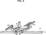
図2に示すように、各垂直接続素子21および水平接続素子31においては磁気抵抗効果素子の磁界反転を行うための磁界反転信号線が別途形成されている。図2の図解では、信号線電流経路41、磁気抵抗効果素子磁界反転下部信号線電流経路42および磁気抵抗効果素子磁界反転上部信号線電流経路43を矢印で示す。すなわち、磁気抵抗効果素子磁界反転下部信号線電流経路42および磁気抵抗効果素子磁界反転上部信号線電流経路43が磁界反転信号線となっている。
【0022】
次に、垂直接続素子21および水平接続素子31を逐次積層するための手順を図3〜図10の模式的レイアウト図および部分拡大図を参照して述べる。
【0023】
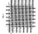
図3の模式的レイアウト図および図4の図3中のA部拡大図には、(+V)電源線PL1(+V)と、(−V)電源線PL1(−V)と、第1段垂直接続素子MR1Vの構成が示されている。
【0024】
図3および図4の図解において、図2に図解したように、第1層(最下層)に電源線(または給電線)PL1(+V)およびPL1(−V)が形成されており、これら電源線PL1(+V)およびPL1(−V)に、図1に図解した垂直接続素子21として機能する磁気抵抗効果磁界スイッチング素子を用いた第1段垂直接続素子MR1Vが接続され、これら磁気抵抗効果磁界スイッチング素子による第1段垂直接続素子MR1Vを駆動するため、第2層磁気抵抗効果磁界スイッチング素子用磁界反転下部信号線SL2と、第3層磁気抵抗効果磁界スイッチング素子用磁界反転上部信号線SL3とが形成されている。
【0025】
図5の模式的レイアウト図および図6の図5中のB部拡大図には、第1段垂直接続素子MR1Vの上に第1段水平接続素子MR1Hを積層した構成が示されている。
すなわち、図1に図解した水平接続素子31として機能する磁気抵抗効果磁界スイッチング素子を用いた第1段水平接続素子MR1Hが設けられ、これら磁気抵抗効果磁界スイッチング素子による第1段水平接続素子MR1Hを駆動するため、第4層磁気抵抗効果磁界スイッチング素子用磁界反転下部信号線SL4と、第5層磁気抵抗効果磁界スイッチング素子用磁界反転上部信号線SL5とが形成されている。
【0026】
図7の模式的レイアウト図および図8の図7中のC部拡大図は、第1段垂直接続素子MR1Vと第1段水平接続素子MR1Hを接続するための、ローカル配線の構成を示す。
【0027】
すなわち、図1に図解した垂直接続素子21として機能する図3および図4に図解した磁気抵抗効果磁界スイッチング素子を用いた第1段垂直接続素子MR1Vと、図1に図解した水平接続素子31として機能する図5および図6に図解した磁気抵抗効果磁界スイッチング素子を用いた第1段垂水平続素子MR1Hとを接続するため、第1段・垂直接続素子・水平接続素子ローカル接続配線1LC(Local Inter-connection) が設けられている。
【0028】
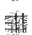
図9の模式的レイアウト図および図10の図9中のD部拡大図は、図8の図解の構成に第2段垂直素子MR2Vを積層した構成を示す。さらに積層するには、上記垂直接続素子と水平接続素子の構成を単に繰り返せば良い。
【0029】
図9および図10に図解の状態は、図7および図8の図解の層の上に、磁気抵抗効果磁界スイッチング素子を用いた第2段垂直接続素子MR2と、この第2段垂直接続素子MR2を駆動するための第6層・第2段磁気抵抗効果磁界スイッチング素子用磁界反転下部信号線SL6−2と、第7層・第2段磁気抵抗効果磁界スイッチング素子用磁界反転上部信号線SL7−2とが形成されている。
【0030】
上記垂直接続素子および水平接続素子として用いられる、磁気抵抗効果磁界スイッチング素子は、抵抗体に磁界を印加することにより電気抵抗値が変化する現象を用いた素子である。本実施の形態においては、上部信号線および下部信号線、たとえば、図4に図解した第1段垂直接続素子MR1Vについては、第2層磁気抵抗効果磁界スイッチング素子用磁界反転下部信号線SL2と、第3層磁気抵抗効果磁界スイッチング素子用磁界反転上部信号線SL3とに電流を流すことにより、磁界が発生し、それにより、磁気抵抗効果磁界スイッチング素子を用いた第1段垂直接続素子MR1Vの抵抗値が変化して、第1段垂直接続素子MR1Vを含む電流経路を確立させる、すなわち、回路を構成することができる。
【0031】
このような、上部信号線および下部信号線に上記磁界発生のために電流を流したり、電流供給を停止するため、上部信号線および下部信号線にはスイッチング素子、たとえば、図29に図解するMOSトランジスタが接続される。このようなトランジスタには、ユーザが希望する回路構成に応じて規定される駆動信号が印加される。
【0032】
磁気抵抗効果磁界スイッチング素子を用いた接続素子、および、磁気抵抗効果磁界スイッチング素子に磁界を印加するための上部信号線および下部信号線の構造については、図29A〜29Iを参照して述べる。
【0033】
なお、磁気抵抗効果素子は、磁気抵抗効果磁界スイッチング素子として機能させる場合は連続的な磁界を印加して導通状態を連続的に維持させ、他方、論理回路素子として機能させるときは瞬間的な磁界を印加して瞬間的な導通状態(反転状態)を発生させることができる。換言すれば、磁気抵抗効果素子は、制御線に印加する電流のパターン(パルスか連続信号か)に応じて、論理回路素子として機能させることもできるし、接続素子として機能させることもできる。論理回路素子として機能させる場合については後述する。
【0034】
論理回路を垂直接続素子および水平接続素子を用いて形成するには、以下のように行う。
【0035】
なお、本発明の実施の形態の半導体集積回路装置としては、上述した磁気抵抗効果磁界スイッチング素子を用いた垂直接続素子と水平接続素子の導通状態(抵抗値が最小の状態)および非導通状態(抵抗値が最大の状態、好ましくは、実質的に無限大の状態)による電流経路の断続によって構成される種々の回路を1または複数構成可能な量の回路素子が事前に組み込まれている。換言すれば、本発明の実施の形態においては、複数の回路素子を、垂直接続素子と水平接続素子の導通状態および非導通状態に応じて組み合わせて所望の回路を構成する。
【0036】
垂直接続素子と水平接続素子の導通状態および非導通状態を指定するため、垂直接続素子および水平接続素子の各々に磁界を印加するための、上部信号線および下部信号線に電流を印加/非印加するスイッチング素子にアドレスを付して、半導体集積回路装置の外部から所望の回路構成に応じたアドレスを印加する。換言すれば、半導体集積回路装置の外部からユーザが希望する回路構成に応じたアドレスを指定して半導体集積回路装置に内蔵されたスイッチング素子、たとえば、トランジスタをオンまたはオフして、上部信号線および下部信号線に電流を供給しまたは供給を停止して、対応する垂直接続素子または水平接続素子に磁界を印加してまたは印加を停止して、垂直接続素子または水平接続素子を導通状態または非導通状態にすることにより、半導体集積回路装置に内蔵された回路素子を組み合わせて、所望の回路を構成することができる。
【0037】
なお、そのような回路を無くして新たな回路を構成したいときは、上記スイッチング素子の信号印加をリセットして、新たな回路構成のための信号をスイッチング素子に印加すればよい。
【0038】
したがって、本発明の実施の形態の半導体集積回路装置は、希望する回路を繰り返して構成して、動作させることができる。
【0039】
さらに、本発明の磁気抵抗効果素子の半導体集積回路装置においては、1つの半導体集積回路装置内にそれぞれ複数の回路素子を用いた回路を複数構成することができる。
【0040】
このような回路を構成するとき、磁気抵抗効果素子は接続素子として使用できるだけでなく、論理演算素子、記憶素子、演算処理素子としても機能させることができる。
【0041】
論理回路を形成するアドレス領域を指定する。具体的には、論理回路として使用する最小領域を指定し、隣接する論理回路から指定した領域の論理機能を独立させるために、上記最小領域を囲む垂直接続素子および水平接続素子をOFFにする(非導通状態にする)。同時に目的とする論理回路に必要な電流経路を指定するために、適宜、垂直接続素子および水平接続素子をONする(導通状態にする)。
【0042】
水平接続素子の一部は、半導体集積回路装置の外に取り出され、スイッチング素子の信号入力素子として使用する。入力信号に応じて、水平接続素子がON/OFFされ、出力に論理回路に応じた出力電圧が出力される。
【0043】
論理回路としての使用が終了したら、指定したアドレス領域を解放し、使用した垂直接続素子および水平接続素子を次の論理回路の構成に用いる。
【0044】
なお、本発明の実施に際しては、スイッチング素子として磁気抵抗効果素子に代えて、抵抗制御素子を用いることもできる。
【0045】
上述した本発明の構想に基づく基本的な論理回路の設定について具体的に説明する。
【0046】
NOT回路
NOT(否定)回路について例示する。
【0047】
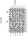
図11A〜11Cは、NOT回路の構成図である。図12はNOT回路の素子の状態を示す図表(グラフ)である。
【0048】
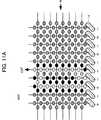
図11Aに示すように、NOT論理回路形成のために電流経路(回路)を設定する。
図11Aでは、白抜きの楕円で示す素子が電流経路となるように設定した素子を示す。白抜きの楕円で示された電流経路には下部の電源線11(+V)、11(−V)が接続されている。白抜きの楕円で示された電流経路が形成されている部分に隣接する黒楕円で示された部分が、NOR回路の論理を他の周辺回路と分離するために隔離部分であり、接続素子をOFF(非導通状態)に設定している。
【0049】
このNOR回路においては、「0」入力のときON(導通状態)になる水平接続素子と、「1」入力のときON(導通状態)になる水平接続素子とを組み込んでいる。このように機能する素子を本発明において回路素子と呼ぶ。このような回路素子としては、磁気抵抗効果素子または抵抗制御素子を用いることができる。以下、磁気抵抗効果素子を用いた場合について例示する。すなわち、制御線に瞬間的な電流を流すと、瞬間的な磁界が磁気抵抗効果素子に作用し、磁気抵抗効果素子は瞬間的に導通状態になるから、高速動作する論理回路素子として使用することができる。この場合、NOR回路を構成する磁気抵抗効果素子の制御線が論理回路素子の入力端子に接続されている。
【0050】
他方、制御線に連続的に電流を流すと、連続的に磁界が磁気抵抗効果素子に作用し、磁気抵抗効果素子は連続して導通状態を維持するから、磁気抵抗効果素子は接続素子として使用することができる。このように回路経路における導通手段として機能する素子を本発明において接続素子と呼ぶ。なお接続手段という場合、磁気抵抗効果磁界スイッチング素子と、これに磁界を印加する上部信号線および下部信号線の磁界印加部分を含む。
【0051】
もちろん、スイッチング素子として磁気抵抗効果素子に代えて抵抗制御素子を用いることができる。
【0052】
回路素子、導通素子および接続素子については、NOR回路に限らず、他の回路においても同様である。
【0053】
次に、図11Bに示すように入力信号が「0」の場合、あらかじめ「0」に対応させている水平接続素子をONにする。これにより出力線に+Vの電圧、すなわち「1」が”0”入力における電流経路にそって出力される。
【0054】
逆に、図11Cに示すように入力信号が「1」の場合、あらかじめ「1」に対応する水平接続素子をONにする。これにより、出力線に−Vの電圧、すなわち「0」が”1”入力における電流経路にそって出力される。
【0055】
論理をまとめると、以下のようになり、NOT回路として動作することが判る。入力信号(1)に対応する水平接続素子をONにすると、出力信号「0」に対応する−Vが出力される。入力信号(0)に対応する水平接続素子をONにすると、出力信号「1」に対応する+Vが出力される。
【0056】
AND回路
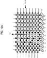
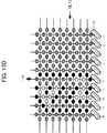
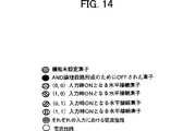
AND(論理積)回路の設定について例示する。図13A〜13Eは、AND回路の構成図である。図14はAND回路内の素子の状態を示すグラフである。
【0057】
論理は以下のようになる。
入力信号(0,0)に対応する、たとえば、磁気抵抗効果素子を用いた水平接続素子をONにすると、出力信号「0」に対応する−Vが出力される。入力信号(1,0)に対応する水平接続素子をONにすると、出力信号「0」に対応する−Vが出力される。入力信号(0,1)に対応する水平接続素子をONにすると出力信号「0」に対応する−Vが出力される。入力信号(1,1)に対応する水平接続素子をONにすると、出力信号「1」に対応する+Vが出力される。
【0058】
図13Aに示すように、AND回路の電流経路を設定する。図面では、白抜きの楕円で示す磁気抵抗素子または抵抗制御素子(以下、磁気抵抗効果素子を例示する)を用いた素子が電流経路となるように設定した素子を示す。
【0059】
図13Bに示すように入力信号が(0,0)の場合、あらかじめ(0,0)に対応させている、磁気抵抗効果素子を用いた水平接続素子をONにする。これにより出力線に−Vの電圧、すなわち「0」が(0,0)入力における電流経路に沿って出力される。
【0060】
図13Cに示すように入力信号が(1,0)の場合、あらかじめ(1,0)に対応させている磁気抵抗効果素子を用いた水平接続素子をONにする。これにより、出力線に−Vの電圧、すなわち「0」が(1,0)入力における電流経路に沿って出力される。
【0061】
図13Dに示すように入力信号が(0,1)の場合、あらかじめ(0,1)に対応させている磁気抵抗効果素子を用いた水平接続素子をONにする。これにより、出力線に−Vの電圧、すなわち「0」が(0,1)入力における電流経路に沿って出力される。
【0062】
図13Eに示すように入力信号が(1,1)の場合、あらかじめ(1,1)に対応させている水平接続素子をONにする。これにより、出力線に+Vの電圧、すなわち「1」が(1,1)入力における電流経路に沿って出力される。
【0063】
OR回路
次に、OR(論理和)回路の設定について例示する。
【0064】
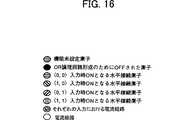
図15A〜15Eは、OR回路の構成図である。図16はOR回路の素子の状態を示すグラフである。
【0065】
論理は以下のようになる。
入力信号(0,0)に対応する磁気抵抗効果素子を用いた水平接続素子をONにすると、出力信号「0」に対応する−Vが出力される。入力信号(1,0)に対応する水平接続素子をONにすると出力信号「1」に対応する+Vが出力される。入力信号(0,1)に対応する水平接続素子をONにすると出力信号「1」に対応する+Vが出力される。入力信号(1,1)に対応する水平接続素子をONにすると出力信号「1」に対応する+Vが出力される。
【0066】
図15Aに示すように、OR回路の電流経路を設定する。図面では、白抜きの楕円で示す素子が電流経路となるように設定した、磁気抵抗効果素子または抵抗制御素子を用いた素子を示す。
【0067】
図15Bに示すように入力信号が(0,0)の場合、あらかじめ(0,0)に対応させている水平接続素子をONにする。これにより出力線に−Vの電圧、すなわち「0」が(0,0)入力における電流経路に沿って出力される。
【0068】
図15Cに示すように入力信号が(1,0)の場合、あらかじめ(1,0)に対応させている水平接続素子をONにする。これにより、出力線に+Vの電圧、すなわち「1」が(1,0)入力における電流経路に沿って出力される。
【0069】
図15Dに示すように入力信号が(0,1)の場合、あらかじめ(0,1)に対応させている水平接続素子をONにする。これにより、出力線に+Vの電圧、すなわち「1」が(0,1)入力における電流経路に沿って出力される。
【0070】
図15Eに示すように入力信号が(1,1)の場合、あらかじめ(1,1)に対応させている水平接続素子をONにする。これにより、出力線に+Vの電圧、すなわち「1」が(1,1)入力における電流経路に沿って出力される。
【0071】
NAND回路
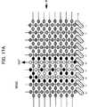
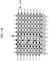
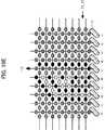
NAND(否定論理積)回路の設定について例示する。
【0072】
図17A〜17Eは、NAND回路の構成図である。図18はNAND回路内の素子の状態を示すグラフである。
【0073】
論理は以下のようになる。
入力信号(0,0)に対応する磁気抵抗効果素子を用いた水平接続素子をONにすると出力信号「1」に対応する+Vが出力される。入力信号(1,0)に対応する水平接続素子をONにすると出力信号「1」に対応する+Vが出力される。入力信号(0,1)に対応する水平接続素子をONにすると出力信号「1」に対応する+Vが出力される。入力信号(1,1)に対応する水平接続素子をONにすると出力信号「0」に対応する−Vが出力される。
【0074】
図17Aに示すように、NAND回路の電流経路を設定する。図面では、白抜きの楕円で示す素子が電流経路となるように設定した、磁気抵抗効果素子または抵抗制御素子を用いた素子を示す。
【0075】
図17Bに示すように入力信号が(0,0)の場合、あらかじめ(0,0)に対応させている水平接続素子をONにする。これにより出力線に+Vの電圧、すなわち「1」が(0,0)入力における電流経路に沿って出力される。
【0076】
図17Cに示すように入力信号が(1,0)の場合、あらかじめ(1,0)に対応させている水平接続素子をONにする。これにより、出力線に+Vの電圧、すなわち「1」が(1,0)入力における電流経路に沿って出力される。
【0077】
図17Dに示すように入力信号が(0,1)の場合、あらかじめ(0,1)に対応させている水平接続素子をONにする。これにより、出力線に+Vの電圧、すなわち「1」が(0,1)入力における電流経路に沿って出力される。
【0078】
図17Eに示すように入力信号が(1,1)の場合、あらかじめ(1,1)に対応させている水平接続素子をONにする。これにより、出力線に−Vの電圧、すなわち「0」が(1,1)入力における電流経路にそって出力される。
【0079】
NOR回路
次に、NOR(否定論理和)回路の設定について例示する。
【0080】
図19A〜19Eは、NOR回路の構成図である。図20はNOR回路内の素子の状態を示すグラフである。
【0081】
論理は以下のようになる。
入力信号(0,0)に対応する磁気抵抗効果素子または抵抗制御素子を用いた水平接続素子をONにすると出力信号「1」に対応する+Vが出力される。
【0082】
入力信号(1,0)に対応する水平接続素子をONにすると出力信号「0」に対応する−Vが出力される。入力信号(0,1)に対応する水平接続素子をONにすると出力信号「0」に対応する−Vが出力される。入力信号(1,1)に対応する水平接続素子をONにすると出力信号「0」に対応する−Vが出力される。
【0083】
図19Aに示すように、NOR回路の電流経路を設定する。図面では、白抜きの楕円で示す素子が電流経路となるように設定した、磁気抵抗効果素子または抵抗制御素子を用いた素子を示す。
【0084】
図19Bに示すように入力信号が(0,0)の場合、あらかじめ(0,0)に対応させている水平接続素子をONにする。これにより出力線に+Vの電圧、すなわち「1」が(0,0)入力における電流経路に沿って出力される。
【0085】
図19Cに示すように入力信号が(1,0)の場合、あらかじめ(1,0)に対応させている水平接続素子をONにする。これにより、出力線に−Vの電圧、すなわち「0」が(1,0)入力における電流経路に沿って出力される。
【0086】
図19Dに示すように入力信号が(0,1)の場合、あらかじめ(0,1)に対応させている水平接続素子をONにする。これにより、出力線に−Vの電圧、すなわち「0」が(0,1)入力における電流経路に沿って出力される。
【0087】
図19Eに示すように入力信号が(1,1)の場合、あらかじめ(1,1)に対応させている水平接続素子をONにする。これにより、出力線に−Vの電圧、すなわち「0」が(1,1)入力における電流経路に沿って出力される。
【0088】
EXOR回路
EXOR(排他的論理和)回路の設定について例示する。
【0089】
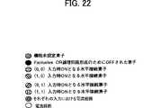
図21A〜21Eは、EXOR回路の説明図である。図22はEXOR回路の素子の状態を示すグラフである。
【0090】
論理は以下のようになる。
入力信号(0,0)に対応する磁気抵抗効果素子または抵抗制御素子を用いた水平接続素子をONにすると出力信号「0」に対応する−Vが出力される。
【0091】
入力信号(1,0)に対応する水平接続素子をONにすると出力信号「1」に対応する+Vが出力される。
【0092】
入力信号(0,1)に対応する水平接続素子をONにすると出力信号「1」に対応する+Vが出力される。
【0093】
入力信号(1,1)に対応する水平接続素子をONにすると出力信号「0」に対応する−Vが出力される。
【0094】
図21Aに示すように、EXOR回路の電流経路を設定する。図面では、白抜きの楕円で示す素子が電流経路となるように設定した、磁気抵抗効果素子または抵抗制御素子を用いた素子を示す。
【0095】
図21Bに示すように入力信号が(0,0)の場合、あらかじめ(0,0)に対応させている水平接続素子をONにする。これにより出力線に−Vの電圧、すなわち「0」が(0,0)入力における電流経路に沿って出力される。
【0096】
図21Cに示すように入力信号が(1,0)の場合、あらかじめ(1,0)に対応させている水平接続素子をONにする。これにより、出力線に+Vの電圧、すなわち「1」が(1,0)入力における電流経路に沿って出力される。
【0097】
図21Dに示すように入力信号が(0,1)の場合、あらかじめ(0,1)に対応させている水平接続素子をONにする。これにより、出力線に+Vの電圧、すなわち「1」が(0,1)入力における電流経路に沿って出力される。
【0098】
図21Eに示すように入力信号が(1,1)の場合、あらかじめ(1,1)に対応させている水平接続素子をONにする。これにより、出力線に−Vの電圧、すなわち「0」が(1,1)入力における電流経路に沿って出力される。
【0099】
Inclusive AND回路
Inclusive AND(排他的論理積)回路の設定について例示する。
【0100】
図23A〜23Eは、Inclusive AND回路の構成図である。図24はInclusive AND回路の素子の状態を示すグラフである。
【0101】
論理は以下のようになる。
入力信号(0,0)に対応する磁気抵抗効果素子を用いた水平接続素子をONにすると出力信号「1」に対応する+Vが出力される。入力信号(1,0)に対応する水平接続素子をONにすると出力信号「0」に対応する−Vが出力される。入力信号(0,1)に対応する水平接続素子をONにすると出力信号「0」に対応する−Vが出力される。入力信号(1,1)に対応する水平接続素子をONにすると出力信号「1」に対応する+Vが出力される。
【0102】
図23Aに示すように、Inclusive AND回路の電流経路を設定する。図面では、白抜きの楕円で示す素子が電流経路となるように設定した、磁気抵抗効果素子または抵抗制御素子を用いた素子を示す。
【0103】
図23Bに示すように入力信号が(0,0)の場合、あらかじめ(0,0)に対応させている水平接続素子をONにする。これにより出力線に+Vの電圧、すなわち「1」が(0,0)入力における電流経路に沿って出力される。
【0104】
図23Cに示すように入力信号が(1,0)の場合、あらかじめ(1,0)に対応させている水平接続素子をONにする。これにより、出力線に−Vの電圧、すなわち「0」が(1,0)入力における電流経路に沿って出力される。
【0105】
図23Dに示すように入力信号が(0,1)の場合、あらかじめ(0,1)に対応させている水平接続素子をONにする。これにより、出力線に−Vの電圧、すなわち「0」が(0,1)入力における電流経路に沿って出力される。
【0106】
図23Eに示すように入力信号が(1,1)の場合、あらかじめ(1,1)に対応させている水平接続素子をONにする。これにより、出力線に+Vの電圧、すなわち「1」が(1,1)入力における電流経路に沿って出力される。
【0107】
Half Adder回路
Half Adder(半加算)回路の設定について例示する。
【0108】
図25A〜25Eは、Half Adder(半加算)回路の構成図である。図26は半加算回路内の素子の状態を示すグラフである。
【0109】
半加算回路は、2進法計算において、(0+0)、(0+1)、(1+0)および(1+1)を計算するものであるので、2入力、2出力で構成される。論理は以下のようになる。
【0110】
上位ビットである入力1信号(0)および下位ビットである入力2信号(0)の組み合わせに対応する磁気抵抗効果素子または抵抗効果素子を用いた水平接続素子をONにすると上位ビットである出力1信号には「0」に対応する−V、下位ビットである出力2信号「0」に対応する−Vが出力される。
【0111】
上位ビットである入力1信号(0)および下位ビットである入力2信号(1)の組み合わせに対応する水平接続素子をONにすると上位ビットである出力1信号には「0」に対応する−V、下位ビットである出力2信号「1」に対応する+Vが出力される。
【0112】
上位ビットである入力1信号(1)および下位ビットである入力2信号(0)の組み合わせに対応する水平接続素子をONにすると上位ビットである出力1信号には「0」に対応する−V、下位ビットである出力2信号「1」に対応する+Vが出力される。
【0113】
上位ビットである入力1信号(1)および下位ビットである入力2信号(1)の組み合わせに対応する水平接続素子をONにすると上位ビットである出力1信号には「1」に対応する+V、下位ビットである出力2信号「0」に対応する−Vが出力される。
【0114】
図25Aに示すように、Half Adder(半加算)回路の電流経路を設定する。図面では、白抜きの楕円で示す素子が電流経路となるように設定した、磁気抵抗効果素子または抵抗制御素子を用いた素子を示す。
【0115】
図25Bに示すように入力1信号が(0)および入力2信号が(0)の場合、あらかじめこの組み合わせに対応させている水平接続素子をONにする。これにより出力1線に−Vの電圧すなわち「0」が(0+0)計算における電流経路にそって出力され、出力2線に−Vの電圧すなわち「0」が(0+0)計算における電流経路にそって出力される。
【0116】
図25Cに示すように入力1信号が(0)および入力2信号が(1)の場合、あらかじめこの組み合わせに対応させている水平接続素子をONにする。これにより出力1線に−Vの電圧すなわち「0」が(1+0)計算における電流経路に沿って出力され、出力2線に+Vの電圧すなわち「1」が(1+0)計算における電流経路に沿って出力される。
【0117】
図25Dに示すように入力1信号が(1)および入力2信号が(0)の場合、あらかじめこの組み合わせに対応させている水平接続素子をONにする。これにより出力1線に−Vの電圧すなわち「0」が(0+1)計算における電流経路に沿って出力され、出力2線に+Vの電圧すなわち「1」が(0+1)計算における電流経路に沿って出力される。
【0118】
図25Eに示すように入力1信号が(1)および入力2信号が(1)の場合、あらかじめこの組み合わせに対応させている水平接続素子をONにする。これにより出力1線に+Vの電圧すなわち「1」が(1+1)計算における電流経路に沿って出力され、出力2線に+Vの電圧すなわち「1」が(1+1)計算における電流経路に沿って出力される。
【0119】
上述したように、本実施例における構成においては、適宜論理式に対応する論理回路を構成するため、従来のMOSトランジスタから構成されるような、論理回路の組み合わせを必要としない。例えば、MOSトランジスタにおいては、OR回路は3個のNANDから構成される場合もあるが、本実施例においては、OR回路以外の論理回路で構成する必要がない。この判点によって、論理回路の所要面積を低減することができる。
【0120】
メモリ
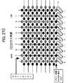
メモリ回路として用いる場合を説明する。図1を参照して説明したように、本実施の形態では、水平接続素子が8段重なっている構造であるので、8ビットの同時記憶ができる。
【0121】
メモリ回路の一例を図27A〜27Cの構成図を参照して説明する。図28はメモリ回路内の素子の状態を示すグラフである。
【0122】
図27Aに示すように、メモリ機能としての電流経路を形成する。図27Aでは、機能未設定素子およびメモリ回路形成のためにOFFされた素子以外の素子が電流経路となる素子に設定されている。ここで、磁気抵抗効果素子または抵抗制御素子を用いた水平接続素子の一部はメモリ素子として用いられる。8段重なっている水平接続素子1〜8のそれぞれは、上の段から下の段に向かって上位ビット(MSB)から下位ビット(LSB)に対応させる。上記ビットの配置の順番は逆であっても良い。
【0123】
メモリの例として、「00110101」を記憶させる一例を図27Bに示す。
「1」に対応する水平接続素子をON(図面◎で示す)にし、「0」に対応する水平接続素子をOFF(図面●で示す)にする。これで書き込みが終了する。読み込み動作は、記憶素子に隣接しており、かつ電源線11に接続されている垂直接続素子をONにすることにより電流が「1」に対応する水平接続素子のみを通ることで、「00110101」に対応する信号が出力線に出力されることにより行われる。本説明では、電源線11を+Vのものを用いたが、電源線11を−Vのものを用いても良い。
【0124】
電源線+Vを使用する場合を正の値の記憶、もしくは図27Cに示すように電源線11(−V)を使用する場合を負の値の記憶に対応させておくこともできる。この場合は負値に対して補数表現で記憶させる必要がないという効果がある。
【0125】
アドレス割り当て法
以上述べた回路における回路素子または接続素子にアドレスを割り当てる場合には、前に例示したAND回路やOR回路といった単機能回路のみならず、機能ブロック単位で割り当てても良い。この場合、三つの使用方法がある。
【0126】
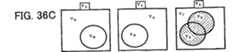
第1の使用方法としては、異なった機能を具備する機能ブロックを、あらかじめアドレスが割り当てられている素子の集合、例えば図36Bにおいて「α」内でそれぞれ異なったアドレス空間を指定することにより、「α」内で異なる処理を同時に実行することができる。例えば、図36Bにより説明すると、「ξ」、「γ」および「ρ」がそれぞれ異なった機能ブロックであることに相当する。
【0127】
第2の使用方法としては、同一機能を具備する機能ブロックを、あらかじめアドレスが割り当てられている素子の集合「α」内でそれぞれ異なったアドレス空間を指定することにより、「α」内で同一の処理を同時に実行することができる。例えば、図36Bを参照して説明すると、「ξ」、「γ」および「ρ」が、それぞれ同一の機能ブロックであることに相当する。この場合は同一機能の処理を、従来例の3倍の効率で処理できることに相当する。
【0128】
第3の使用方法としては、いわゆる並列処理を実現するものであって、例えば同一機能を具備する機能ブロックを、あらかじめアドレスが割り当てられている素子の集合「α」内でそれぞれ異なったアドレス空間を指定することにより、「α」内で同一の処理を同時に相互に関連させながら実行することができる。例えば、図36Bを参照して説明すると、「ξ」、「γ」および「ρ」が同一の機能ブロックで並列処理におけるクライアント領域であることに相当する。また、「θ」領域には、並列処理におけるサーバー領域の機能が割り当てられる。この場合は並列処理を、従来例のように4個の論理チップに分散させる必要は無く、一つの素子の集合「α」内で実現することができる。
【0129】
命令処理系において、異なった機能ブロック単位で各クラス間の相互依存関係が生じた場合、すなわち従来のパイプライン処理における問題点であるパイプラインハザードに対応する障害が発生した場合、例えば、パイプラインハザードのカテゴリーの中で、分岐命令に起因する制御ハザード、あるいはデータハザードに関するデータフロー依存、逆依存、出力依存の関係に対応する問題が生じた場合は、以下に示す手段で回避できる。
【0130】
特定の機能ブロックで待ち時間が長時間発生する場合、対象となっているアドレスをバッファアドレス空間に移し、論理演算に必要なアドレス空間およびメモリ空間を一時的に解放する。そして、待ち原因となっている機能ブロックにアドレスを割り当て、依存関係を消去する。逆依存、出力依存のある場合も同様である。すなわち、機能ブロック単位でパイプラインとして処理することが可能になり、演算領域およびメモリ領域をアドレスの変更のみで、プログラム実行とともに最適化することができる。
【0131】
図36Bを参照して説明する。「θ」領域に機能が割り当てられていないとする。「γ」領域に「ρ」領域の処理待ちにより待ち時間が長時間発生している場合、「γ」領域の機能ブロックを一時的に「θ」領域に移し、「γ」領域に「ρ」領域の機能を生成する。「ξ」領域をサーバーとして、「γ」領域と「ρ」領域による並列処理を行い、しかるのちに「γ」領域に元の機能を戻し「待ち」を解消する。このように、機能ブロック単位で、依存関係が生じた場合においても、依存関係を直ちに解消することができる。
【0132】
また、入力信号が時間と共に大きく変動するような系で、かつ入力信号の変化に応じてプログラムの処理内容が異なる場合において、処理速度の向上を図ることができる。すなわち、従来技術においては、入力信号の変化に応じて、分岐命令により最適論理回路が選択され実行される。実行過程においては、空間的に機能分離された論理素子およびメモリ素子を使用するため、次に来る入力信号の変化を機能単位で予測する機能は付加できない。
一方、本実施の形態によれば、入出力信号を予測し、あらかじめ次に使用するであろう論理機能を準備することで、処理速度の向上を図ることができる。さらに異なった入力信号に対し、複数の論理機能ブロックを並列処理することも可能である。
【0133】
図36Bを参照して説明する。「ξ」領域、「γ」領域および「ρ」領域にそれぞれ、入力信号の変化を3通りに予測した機能ブロックを割り当てておく。ここで、「ξ」領域に適合した入力信号が入力したとすると、「ξ」領域で処理を行う。「ρ」領域および「γ」領域の機能は直ちにアドレス解放により消滅させ、直ちに次の入力信号を予測した処理機能を生成しておく。「θ」領域は、入力信号を予測し処理機能空間を予測するための、機能領域を生成しておく。
【0134】
次に、本発明の集積回路装置の製造方法について、製造工程断面図を参照して説明する。
本発明の集積回路装置の製造方法は、任意の回路機能として作用する空間を次々に生成および解放を繰り返すことによって、素子の機能を時間的に分割かつ空間的に分割して機能する複数の回路機能を備えた集積回路装置の製造方法であって、磁気抵抗効果素子にアドレスを割り当てるためのトランジスタ領域を形成する工程と、磁気抵抗効果素子を積層して順次形成する工程とにより実現される。
【0135】
例えば、半導体基板(例えばシリコンウエハ)上に、論理回路機能およびメモリ機能を担う素子が磁気抵抗効果素子を積層して構成されている領域と、磁気抵抗効果素子から構成される垂直接続素子および水平接続素子のアドレスを指定するMOSトランジスタから構成される周辺回路領域とから構成される。上記MOS回路部分は、アドレス指定により磁気抵抗効果素子をON/OFFする電流を供給する。
【0136】
集積回路装置の製造は、一例として、図1〜図10の模式的に示したレイアウト図及び部分拡大図に従って順次行えば良い。図1〜図10においては、垂直接続素子が6×6の配置および水平接続素子が7×7の配置を例示してあるが、これは説明の便宜のためであって、垂直接続素子および水平接続素子の配列数の制限はない。
【0137】
具体的には、集積回路装置は、以下の工程を経て作製される。以下、模式的に示した製造工程断面図を用いて説明する。
【0138】
工程1:図29Aに示すように、半導体基板(例えばシリコンウエハ)111上に、MOSトランジスタ121から構成される周辺回路領域120を作製する。すなわち、素子分離(図示せず)の形成工程、ウエル112の形成工程、ソース122およびドレイン123の形成工程、ゲート125の形成工程を行い、MOSトランジスタ121から構成される周辺回路領域120を作製する。
【0139】
工程2:図29Bに示すように、層間絶縁膜131の形成工程、コンタクトホール(ビアホール)132の形成およびコンタクトホール132に導電性材料で埋め込み、プラグ133を形成する工程、配線(例えば金属配線)を形成する配線形成工程を行い、プラグ133に接続するMOSトランジスタの配線135および磁気抵抗効果素子の電源供給線137を形成する。
【0140】
工程3:図29Cに示すように、層間絶縁膜141を形成した後、磁界反転用制御線143を形成する。
【0141】
工程4:図29Dに示すように、後に形成される磁気抵抗効果素子の磁界反転機能層と電源供給線137を接続する接続用コンタクト145を形成する。
【0142】
工程5:図29Eに示すように、層間絶縁膜141上に磁界反転機能層151を形成する。
【0143】
工程6:図29Fに示すように、磁界反転機能層151表面が露出するように層間絶縁膜161を形成した後、周辺回路領域のMOSトランジスタ121に接続されている配線135に達するビアホールを形成した後、そのビアホールを埋め込むプラグ163を形成する。
【0144】
工程7:図29Gに示すように、周辺回路領域のMOSトランジスタ121および磁気抵抗効果素子151の第2の配線(例えば金属配線)171を形成する。
【0145】
工程8:図29Hに示すように、前記工程3から前記工程7のプロセスを繰り返し、磁界反転用制御線143、磁気抵抗効果素子151および周辺回路領域のMOSトランジスタ121および磁気抵抗効果素子151の第2の配線(例えば金属配線)171を積層形成する。
【0146】
工程9:図29Iに示すように、さらに、工程(3)から工程(7)のプロセスを繰り返した結果、磁気抵抗効果素子151および周辺回路領域のMOSトランジスタ121および磁気抵抗効果素子151の第2の配線(例えば金属配線)171を、4層積層した状態に形成する。図29Iは図29Fに示した状態から、工程(3)から工程(7)のプロセスを2回繰り返した場合を示す。
【0147】
上記集積回路装置の製造方法によれば、工程(3)から工程(7)のプロセスを繰り返すことによって、電源線、垂直接続素子9層および水平接続素子8層の機能構造を繰り返し積層して、8ビットの構成を形成することができる。また、垂直接続素子17層および水平接続素子16層の構造を繰り返し積層することで、16ビットの構成にすることもできる。また、垂直接続素子33層および水平接続素子32層の構造を繰り返し積層することで32ビットの構成にすることもできる。
【0148】
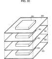
また、電源線、垂直接続素子9層、および水平接続素子8層の機能構造を繰り返し積層する構成において、各機能構造間にシリコンをエピタキシャル成長させることで、図29I、図30の構成図に示すように、MOSトランジスタから構成される周辺回路領域120を各機能構造層毎に形成することができる。図30において、MOSトランジスタから構成される周辺回路領域120上には、磁気抵抗効果素子から構成される論理機能およびメモリ機能領域150が形成されていて、それらは複数層(図面では4層)に積層されている。
【0149】
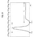
上記磁気抵抗効果素子の磁界反転に要する時間はピコ秒(psec)程度である。そのため、100GHzのスイッチング速度が可能となる。そこで、10GHzで駆動できる周辺部のMOSトランジスと組み合わせた場合の磁気抵抗効果素子に流れるタイミングによる電流の一例を図31に示す。図31に示すように、ONおよびOFFを繰り返し、磁界反転電流IMRが頻繁に流れる水平接続素子により、出力線に磁界反転電流も流れるが、磁界反転に要する電圧と電源電圧が異なるため、磁界反転電流IMRと論理回路動作電流ILOとは容易に区別することができる。図面では、T=0からT=T1までが磁界反転電流IMRとなり、T=T1以降が論理回路動作電流ILOとなっていることからも明らかである。
【0150】
図32A〜32Iを参照して、本発明の別の集積回路装置の製造方法について、以下に説明する。
【0151】
この集積回路装置の製造方法は、任意の回路機能として作用する空間を次々に生成および開放を繰り返すことによって、素子の機能を時間的に分割かつ空間的に分割して機能する複数の回路機能を備えた集積回路装置の製造方法であって、例えば抵抗制御素子にアドレスを割り当てるためのトランジスタ領域を形成する工程と、抵抗制御素子を積層して順次形成する工程とにより実現される。
【0152】
例えば、半導体基板(例えばシリコンウエハ)上に、論理回路機能およびメモリ機能を担う素子が抵抗制御素子を積層して構成されている部分と、抵抗制御素子から構成される垂直接続素子および水平接続素子のアドレスを指定するMOSトランジスタから構成される周辺回路領域とから構成される。上記MOS回路部分は、アドレス指定により抵抗制御素子をON/OFFする電流を供給する。
具体的には、集積回路装置は、以下の工程を経て作製される。以下、模式的に示した製造工程断面図を用いて説明する。
【0153】
工程1:図32Aに示すように、半導体基板(例えばシリコンウエハ)111上に、MOSトランジスタ121から構成される周辺回路領域120を作製する。すなわち、素子分離(図示せず)の形成工程、ウエル112の形成工程、ソース122およびドレイン123の形成工程、ゲート125の形成工程を行い、MOSトランジスタ121から構成される周辺回路領域120を作製する。
【0154】
工程2:図32Bに示すように、層間絶縁膜131の形成工程、コンタクトホール132の形成およびコンタクトホール132を導電性材料で埋め込み、プラグ133を形成する工程、配線(例えば金属配線)を形成する配線工程を行い、プラグ133に接続するMOSトランジスタの配線135および抵抗制御素子の電源供給線137を形成する。
【0155】
工程3:図32Cに示すように、層間絶縁膜141を形成する。
【0156】
工程4:図32Dに示すように、抵抗制御素子と電源供給線の接続およびヒーター用コンタクト245を形成する。
【0157】
工程5:図32Eに示すように、層間絶縁膜141上に抵抗制御素子のカルコゲナイド層251を形成する。
【0158】
工程6:図32Fに示すように、抵抗制御素子のカルコゲナイド層251表面が露出するように層間絶縁膜161を形成した後、周辺回路領域のMOSトランジスタ121に接続されている配線135に達するビアホールを形成した後、そのビアホールを埋め込むプラグ163を形成する。
【0159】
工程7:図32Gに示すように、埋め込むプラグ163に接続するように周辺回路領域120の第2の配線(例えば金属配線)171を形成するとともに抵抗制御素子のカルコゲナイド層251に接続する第2の配線(例えば金属配線)171を形成する。
【0160】
工程8:図32Gに示すように、前記工程3から前記工程7のプロセスを繰り返し、周辺回路領域120の埋め込むプラグ163、抵抗制御素子のヒーター用コンタクト245、抵抗制御素子のカルコゲナイド層251、および周辺回路領域120の第2の配線(例えば金属配線)および抵抗制御素子の第2の配線(例えば金属配線)171を積層形成する。
【0161】
工程9:図32Hに示すように、さらに、工程3から工程7のプロセスを繰り返した結果、抵抗制御素子のカルコゲナイド層251および周辺回路領域120のおよび抵抗制御素子の第2の配線(例えば金属配線171)を、4層積層した状態に形成する。図32Iは図32Gに示した状態から、工程3から工程7のプロセスを2回繰り返した場合を示す。
【0162】
上記集積回路装置の製造方法によれば、工程3から工程7のプロセスを繰り返すことによって、電源線、垂直接続素子を9層および水平接続素子を8層の機能構造を繰り返し積層して、8ビットの構成を形成することができる。また、垂直接続素子を17層および水平接続素子を16層の構造を繰り返し積層することで、16ビットの構成にすることもできる。また、垂直接続素子を33層および水平接続素子を32層の構造を繰り返し積層することで32ビットの構成にすることもできる。
【0163】
また、電源線、垂直接続素子を9層および水平接続素子を8層の機能構造を繰り返し積層する構成において、各機能構造間にシリコンをエピタキシャル成長させることで、図32I、33の構成図に示すように、MOSトランジスタから構成される周辺回路領域120を各機能構造毎に形成することができる。図33において、MOSトランジスタから構成される周辺回路領域120上には、抵抗制御素子から構成される論理機能およびメモリ機能領域150が形成されていて、それらは複数層(図面では4層)に積層されている。
【0164】
上記製造方法では、各階層を抵抗制御素子から構成される論理機能およびメモリ機能領域150で形成したが、任意の階層を前記説明した磁気抵抗効果素子から構成される論理機能およびメモリ機能領域150で形成することも可能である。すなわち、一つの集積回路装置において、論理機能およびメモリ機能領域150は、磁気抵抗効果素子から構成されるものと抵抗制御素子から構成されるものを混在させることも可能である。
【0165】
以上、説明したように本発明の集積回路のアーキテクチャによれば、従来技術のように論理素子を機能別に空間に固定して割り当てることは行わず、論理素子の機能は、時間(クロック進行)とともに動的にアドレスを確保し、かつ解放し、これを繰り返すことができる。これによって、一つの論理素子は複数の機能を持つことが可能になるので、集積回路の空間的な体積を増大させることなく機能的な容量を増大させることができる。また集積回路の構造を3次元立体構造とすることによって、機能を実現するための空間体積を著しく増大させることができる。よって、最小限の素子の構成によって多機能な集積回路を構成することが可能になる。
【0166】
本発明の集積回路装置のアーキテクチャによれば、従来技術のように集積回路を機能別に空間に固定して割り当てることは行わず、集積回路の機能および集積回路の素子の機能は、時間(クロック進行)とともに動的にアドレスを確保し、かつ解放し、これを繰り返すことができる。これによって、一つの集積回路もしくは集積回路の素子は複数の機能を持つことができるので、集積回路装置の空間的な体積を増大させることなく機能的な容量を増大させることができる。また集積回路装置の構造を3次元立体構造とすることによって、機能を実現するための空間体積を著しく増大させることができる。よって、最小限の集積回路の構成によって多機能な集積回路装置を構成することが可能になる。
【0167】
本発明の集積回路装置の動作方法によれば、従来技術のように集積回路を機能別に空間に固定して割り当てることは行わず、集積回路の機能および集積回路の素子の機能は、時間(クロック進行)とともに動的にアドレスを確保し、かつ解放し、これを繰り返す。これによって、一つの集積回路および集積回路の素子に複数の機能を持たせることが可能になるので、集積回路装置の空間的な体積を増大させることなく機能的な容量を増大させることが可能になる。また集積回路装置の構造を3次元立体構造とすることによって、機能を実現するための空間体積を著しく増大させることができる。よって、この動作方法を採用することによって、多機能な集積回路を最小限の素子構成によって実現することを可能にし、また多機能な集積回路装置を最小限の集積回路構成によって実現することを可能にする。
【0168】
本発明の集積回路装置によれば、集積回路を全解放させる動作をするもの、部分解放させる動作をするもの、もしくは部分解放させかつ全解放させる動作をするものからなり、かつ集積回路の素子を全解放させる動作をするもの、部分解放させる動作をするもの、もしくは部分解放させかつ全解放させる動作をするものからなるので、従来技術のように集積回路を機能別に空間に固定して割り当てることは行わず、集積回路の機能は、時間(クロック進行)とともに動的にアドレスを確保し、かつ解放し、これを繰り返すことができる。これによって、一つの集積回路および集積回路の素子に複数の機能を持たせることが可能になるので、集積回路装置の空間的な体積を増大させることなく機能的な容量を増大させることが可能になる。また集積回路装置の構造を3次元立体構造として、機能を実現するための空間体積を著しく増大させることができる。よって、最小限の素子の構成によって、また最小限の集積回路の構成によって、多機能な集積回路装置を構成することが可能になる。
【0169】
本発明の集積回路装置の製造方法によれば、磁気抵抗効果素子および抵抗制御素子のうちのどちらか一方もしくは両方にアドレスを割り当てるためのトランジスタ領域を形成する工程と、前記磁気抵抗効果素子および抵抗制御素子のうちのどちらか一方もしくは両方を積層して順次形成する工程とを行うので、3次元立体構造の集積回路装置の構造が実現でき、これによって、集積回路装置の空間体積を著しく増大させることが可能になる。また従来技術のように論理素子を機能別に空間に固定して割り当てることは行わず、時間(クロック進行)とともに動的にアドレスを確保し、かつ解放し、これを繰り返す機能を有する集積回路もしくは素子を構成することができる。これによって、一つの集積回路もしくは素子に複数の機能を持たせることが可能になるので、集積回路装置の空間的な体積を増大させることなく機能的な容量を増大させることが可能になる。さらに、露光装置の露光面積に制限されずに論理回路機能を拡張できるという著しい効果がある。
【0170】
集積回路のアーキテクチャは、任意の回路機能として作用する空間を次々に生成および解放を繰り返すことによって、素子の機能を時間的に分割かつ空間的に分割して使用するものである。上記回路機能としての論理素子は、あらかじめクロック周波数の進行、すなわち、時間の経過とともにその機能が動的に設定されていて、作用終了後に設定状態が動的に消滅するものである。上記回路機能としてのメモリ素子は、論理素子およびメモリ素子の空間的区別なしに、適宜そのアドレスが動的に設定され、かつ消滅するものからなる。すなわち、特定の素子に対して一義的に機能を設定せず、任意の時間で任意の素子に機能を設定することにより、時間(クロック進行)とともに動的にアドレスを確保し、かつ解放し、これを繰り返す機能を実現するための空間体積を著しく増大させることが可能になる。
【0171】
以上を一般化して述べる。
本発明の代表的な集積回路のアーキテクチャは、時間の経過tn(n=0,1,・・・,n)とともに回路機能が異なる素子の集合であって、時間の経過tnとともに異なる回路機能の部分が素子の全体集合である。すなわち、時間の経過tnとともに回路機能が変化する素子によって集積回路が構成され、時間の経過tnとともに異なる回路機能の部分が全素子にわたっているものである。
【0172】
第2の集積回路のアーキテクチャは、時間の経過tn(n=0,1,・・・,n)とともに回路機能が異なる素子の集合において、時間の経過tnとともに回路機能の異なる部分が任意の個数の部分集合となっている。すなわち、時間の経過tnとともに回路機能が変化する素子によって集積回路が構成され、時間の経過tnとともに回路機能の異なる部分が全素子のうち任意の個数になっているものである。
【0173】
第3の集積回路のアーキテクチャは、時間の経過t0、t1、t2、t3・・・tn(ただし、nは任意の整数)とともに回路機能が異なる素子の集合において、時間の経過t0、t1、t2、t3・・・tnとともに回路機能の異なる部分が任意の経過時間tkにおいては全体集合であり、かつ任意の経過時間th(ただし、k≠h)では任意の個数の部分集合となっているものである。すなわち、時間の経過t0、t1、t2、t3・・・tnとともに回路機能が変化する素子によって集積回路が構成され、任意の時間経過においては、時間の経過t0、t1、t2、t3・・・tnとともに異なる回路機能の部分が全素子にわたっているものであり、また別の任意の時間経過においては、時間の経過t0、t1、t2、t3・・・tnとともに回路機能の異なる部分が全素子のうち任意の個数になっているものである。
【0174】
次に、本発明の集積回路装置のアーキテクチャは、任意の回路機能として作用する空間を次々に生成および解放を繰り返すことによって、素子の機能を時間的に分割かつ空間的に分割して使用するものである。上記回路機能としての論理回路は、あらかじめクロック周波数の進行とともにその機能が動的に設定されていて、作用終了後に動的に消滅するものである。上記回路機能としてのメモリ回路は、論理回路およびメモリ回路の空間的区別なしに、適宜そのアドレスが動的に設定され、かつ消滅するものからなる。すなわち、特定の回路に対して一義的に機能を設定せず、任意の時間で任意の素子に機能を設定することにより、時間(クロック進行)とともに動的にアドレスを確保し、かつ解放し、これを繰り返す機能を実現するための空間体積を著しく増大させることが可能になる。
【0175】
第1の集積回路装置のアーキテクチャでは、時間の経過t0、t1、t2、t3・・・tx(ただし、xは任意の整数)とともに機能が異なる集積回路の集合において、時間の経過t0、t1、t2、t3・・・txとともに機能が異なる部分が集積回路の全体集合となっている。すなわち、時間の経過t0、t1、t2、t3・・・tnとともに回路機能が変化する集積回路によって集積回路装置が構成され、時間の経過t0、t1、t2、t3・・・tnとともに異なる回路機能の部分が全集積回路にわたっているものである。そして、上記集積回路は、前記説明した第1〜第3の集積回路のアーキテクチャのいずれかにより構成されている。
【0176】
第2の集積回路装置のアーキテクチャでは、時間の経過t0、t1、t2、t3・・・tx(ただし、xは任意の整数)とともに機能が異なる集積回路の集合において、時間の経過t0、t1、t2、t3・・・txとともに機能が異なる部分が任意の個数の部分集合となっている。すなわち、時間の経過t0、t1、t2、t3・・・tnとともに回路機能が変化する集積回路によって集積回路装置が構成され、時間の経過t0、t1、t2、t3・・・tnとともに回路機能の異なる部分が全集積回路のうち任意の個数になっているものである。そして、上記集積回路は、前記説明した第1〜第3の集積回路のアーキテクチャのいずれかにより構成されている。
【0177】
第3の集積回路装置のアーキテクチャでは、時間の経過t0、t1、t2、t3・・・tx(ただし、xは任意の整数)とともに機能が異なる集積回路の集合において、時間の経過t0、t1、t2、t3・・・tfとともに機能の異なる部分が任意の経過時間tkにおいては全体集合であり、かつ任意の経過時間tg(ただしf≠g)では任意の個数の部分集合となっている。すなわち、時間の経過t0、t1、t2、t3・・・tnとともに回路機能が変化する集積回路によって集積回路装置が構成され、任意の時間経過においては、時間の経過t0、t1、t2、t3・・・tnとともに異なる回路機能の部分が全集積回路にわたっているものであり、また別の任意の時間経過においては、時間の経過t0、t1、t2、t3・・・tnとともに回路機能の異なる部分が全集積回路のうち任意の個数になっているものである。そして、上記集積回路は、前記説明した第1〜第3の集積回路のアーキテクチャのいずれかにより構成されている。
【0178】
これら第1から第3の集積回路のアーキテクチャは、それぞれ単独に用いてもよいし、もしくは第1から第3の集積回路装置のアーキテクチャと適宜組み合わせて用いても良い。すなわち、時間の経過T1、T2、T3・・・Tmにおいて、任意の経過時間Tq(Tqにおいてさらに分割された時間の経過t0、t1、t2、t3・・・tnが経過している)において、第1から第3の集積回路の任意のアーキテクチャを用いて良い。あるいは、第1の集積回路のアーキテクチャを、第1から第3の集積回路のアーキテクチャと適宜組み合わせて用いても良い。あるいはまた、第2の集積回路のアーキテクチャを、第1から第3の集積回路のアーキテクチャと適宜組み合わせて用いても良い。あるいはまた、第3の集積回路のアーキテクチャを、第1から第3の集積回路のアーキテクチャと適宜組み合わせて用いても良い。
【0179】
次に、本発明の第1の集積回路の動作方法について、図34Aにより、以下に説明する。
図34Aに示すように、まず、素子の集合「A」を構成する個々の素子にアドレスを割り当てておく。次に回路機能の設定予定領域にアドレスを指定することにより「A」中でアドレスを指定された複数の「Bi」(ただし、i=1,2,3,・・・)の回路機能領域を生成する。このようにして、「B」領域が任意の回路機能として作用する空間を生成する第1の段階が行われる。上記回路機能領
域は、次式で表される。
【0180】
A⊇(B=ΣBi)(ただし、i=1,2,3,・・・)
【0181】
上記第1の段階の「B」領域における部分集合「Bi」が、B=ΣBi=ΣBip+ΣBiq(ただし、ip=1,2,3,・・・、iq=1,2,3,・・・、かつip+iq≦i)で表される、論理回路機能として作用する「Bip」空間およびメモリ回路機能として作用する「Biq」空間を構成してもよい。
【0182】
または、上記第1の段階の「B」領域における部分集合「Bi」の全てが論理回路機能として作用する空間を構成してもよい。
【0183】
または、上記第1の段階の「B」領域における部分集合「Bi」の全てがメモリ回路機能として作用する空間を構成してもよい。
【0184】
次いで、上記「Bi」を用いて演算処理および情報処理を行った後、「Bi」(ただし、i=1,2,3,・・・)からなる全領域である「B」の回路機能のアドレスを解放する。
【0185】
次に回路機能の設定予定領域にアドレスを指定することにより「A」中でアドレスを指定された複数の「Cj」(ただし、j=1,2,3,・・・)の回路機能領域を生成する。このようにして、「C」領域が任意の回路機能として作用する空間を生成する第2の段階が行われる。この回路機能領域は、次式で表される。
【0186】
A⊇(C=ΣCj)(ただし、j=1,2,3,・・・)
【0187】
上記第2の段階の「C」領域における部分集合「Cj」は、C=ΣCj=ΣCjr+ΣCjs(ただし、jr=1,2,3,・・・、js=1,2,3,・・・、かつjr+js≦j)で表される、論理回路機能として作用する「Cjr」空間およびメモリ回路機能として作用する「Cjs」空間を構成してもよい。
【0188】
または、上記第2の段階の「C」領域における部分集合「Ci」の全てが論理回路機能として作用する空間を構成してもよい。
【0189】
または、上記第2の段階の「C」領域における部分集合「Ci」の全てがメモリ回路機能として作用する空間を構成してもよい。
【0190】
次いで、「Cj」を用いて演算処理および情報処理を行った後、「Cj」(ただし、j=1,2,3,・・・)からなる全領域である「C」の回路機能のアドレスを解放する。
【0191】
次に回路機能の設定予定領域にアドレスを指定することにより「A」中でアドレスを指定された複数の「Dk」(ただし、k=1,2,3,・・・)の回路機能領域を生成する。このようにして、「D」領域が任意の回路機能として作用する空間を生成する第3の段階が行われる。この回路機能領域は、次式で表される。
【0192】
A⊇(D=ΣDk)(ただし、k=1,2,3,・・・)
【0193】
上記第3の段階の「C」領域における部分集合「Cj」が、D=ΣDk=ΣDkt+ΣDku(ただし、kt=1,2,3,・・・、ku=1,2,3,・・・、かつkt+ku≦k)で表される、論理回路機能として作用する「Dkt」空間およびメモリ回路機能として作用する「Dku」空間を構成してもよい。
【0194】
または、上記第3の段階の「D」領域における部分集合「Dk」の全てが論理回路機能として作用する空間を構成してもよい。
【0195】
または、上記第3の段階の「D」領域における部分集合「Dk」の全てがメモリ回路機能として作用する空間を構成してもよい。
【0196】
次いで、「Dk」を用いて演算処理および情報処理を行った後、「Dk」(ただし、k=1,2,3,・・・)からなる全領域である「D」の回路機能のアドレスを解放する。
【0197】
さらに、同様に第4の段階、第5の段階、さらには第nの段階(ただし、n=1,2,3,・・・)とを順に行うことにより、任意の回路機能として作用する空間を次々に生成および解放を繰り返すことによって、素子の機能を時間分割して使用できる。
【0198】
次に、本発明の第2の集積回路の動作方法について、図34Bおよび図35により、以下に説明する。
【0199】
図34Bに示すように、あらかじめアドレスが割り当てられている素子の集合「α」の任意の領域に、アドレスを指定することにより「α」の部分集合である「βi」(ただし、i=1,2,3,・・・)の第1の回路機能形成予定領域を生成する。このようにして、「βi」領域が任意の回路機能として作用する空間を生成する第1の段階を行う。この第1の回路機能形成予定領域は、次式で表される。
【0200】
α⊇(β=Σβi)(ただし、i=1,2,3,・・・)
【0201】
ここで、「β」領域における部分集合「βi」は、論理回路機能として作用する「βip」空間およびメモリ回路機能として作用する「βiq」空間を構成している。この空間は次式で表される。
【0202】
β=Σβi=Σβip+Σβiq(ただし、ip=1,2,3・・・、iq=1,2,3・・・、かつip+iq≦i)
【0203】
または、「β」領域における部分集合「βi」の全てが論理回路機能として作用する空間を構成していてもよい。
【0204】
または、「β」領域における部分集合「βi」の全てがメモリ回路機能として作用する空間を構成していてもよい。
【0205】
ここで、それぞれの「βi」領域は、後述するように、基本的な論理回路から構成される機能グループもしくはメモリ機能を具備するグループである。「βi」の論理機能は、最小にはAND回路とかOR回路といった基本的な論理素子である。もしくは、最小ビットを記憶するメモリ素子である。もしくは、「βi」の論理機能においては、例えば画像処理マクロユニット、音声処理マクロユニット、アナログデジタル変換マクロユニットもしくはデジタルアナログ変換マクロユニットといった、所望の目的を実現するための機能単位であっても良い。もしくは、「βi」のメモリ機能は、キャッシュメモリやバッファメモリといった機能単位であっても良い。
【0206】
次に、「βi」(ただし、i=1,2,3,・・・)の論理回路機能およびメモリ回路機能を使用後に、アドレスを解放する。アドレスの解放は「β」の論理回路機能およびメモリ回路機能の全領域でも良いし、もしくは「β」領域中の一部の「βi」(ただし、i=1,2,3,・・・)に係る論理回路機能およびメモリ回路機能領域でも良い。この段階でアドレスが指定されていない領域は、図2に示す「β」から解放された領域「τ」、および「β」の補集合の領域「δ」から構成される「τ∪δ」である。この「τ∪δ」の領域に、新たな回路機能形成予定領域「ε」を形成する。「ε」は複数の回路機能形成予定領域から構成される。図1の(b)に示すように、領域「ε」と、「β」から解放されずに残っている「φ」(φ⊆β)領域から構成される第2の回路機能形成予定領域を生成する。このようにして、「ε∪φ」領域が任意の回路機能として作用する空間を生成する第2の段階を行う。この第2の回路機能形成予定領域は次式で表すことができる。
【0207】
(ε∪φ=Σλj)⊆α(ただし、j=1,2,3,・・・)
【0208】
「ξ∪γ∪ρ」領域における部分集合「ζk」は、論理回路機能として作用する「ζkt」空間およびメモリ回路機能として作用する「ζku」空間を構成する。この構成は次式で表すことができる。
【0209】
ξ∪γ∪ρ=Σζk=Σζkt+Σζku(ただし、kt=1,2,3,・・・、ku=1,2,3,・・・、かつkt+ku≦k)
【0210】
または、「ξ∪γ∪ρ」領域における部分集合「ζk」の全てが論理回路機能として作用する空間を構成してもよい。
【0211】
または、「ξ∪γ∪ρ」領域における部分集合「ζk」の全てがメモリ回路機能として作用する空間を構成してもよい。
【0212】
「ξ」は、「β」領域からアドレス解放されずに残っている領域「φ」および「ε」領域からアドレス解放されずに残っている領域「γ」と独立に、あるいは連携して演算処理を行う。
【0213】
さらに、同様に第4の段階、第5の段階、さらには第nの段階(ただし、n=1,2,3,・・・)を行うことにより、論理回路機能かつメモリ回路機能として作用する空間、もしくは論理回路機能またはメモリ回路機能として作用する空間を次々に生成および解放を繰り返すことにより、素子の機能を時間分割して使用できる。
【0214】
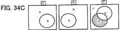
次に、本発明の第3の集積回路の動作方法について、図34Cにより、以下に説明する。
図34Cに示すように、あらかじめアドレスが割り当てられている素子の集合「Λ」の任意の領域に、アドレスを指定することにより「Λ」の部分集合である「Φi」(ただし、i=1,2,3,・・・)の第1の回路機能形成予定領域を生成する。このようにして、「Φ」領域が任意の回路機能として作用する空間を生成する第1の段階を行う。この第1の回路機能形成予定領域は、次式で表される。
【0215】
Λ⊇(Φ=ΣΦi)(ただし、i=1,2,3,・・・)
【0216】
上記第1の段階の「Λ」領域における部分集合「Φi」は、Φ=ΣΦi=ΣΦip+ΣΦiq(ただし、ip=1,2,3,・・・、iq=1,2,3,・・・、かつip+iq≦i)で表される、論理回路機能として作用する「Φip」空間およびメモリ回路機能として作用する「Φiq」空間を構成する。
【0217】
または、上記第1の段階の「Φ」領域における部分集合「Φi」の全てが論理回路機能として作用する空間を構成してもよい。
【0218】
または、上記第1の段階の「Φ」領域における部分集合「Φi」の全てがメモリ回路機能として作用する空間を構成してもよい。
【0219】
次いで、上記「Φi」を用いて演算処理および情報処理を行った後、「Φi」(ただし、i=1,2,3,・・・)からなる全領域である「Φ」の回路機能のアドレスを解放する。
【0220】
次に回路機能の設定予定領域にアドレスを指定することにより「Λ」の中でアドレスを指定された複数の「Ψj」(ただし、j=1,2,3,・・・)の回路機能領域を生成する。このようにして、「Ψ」領域が任意の回路機能として作用する空間を生成する第2の段階が行われる。この回路機能領域は、次式で表される。
【0221】
Λ⊇(Ψ=ΣΨj)(ただし、j=1,2,3,・・・)
【0222】
上記「Ψ」領域における部分集合「Ψj」は、Ψ=ΣΨj=ΣΨjr+ΣΨjs(ただし、jr=1,2,3,・・・、js=1,2,3,・・・、かつjr+js≦j)で表される、論理回路機能として作用する「Ψjr」空間およびメモリ回路機能として作用する「Ψjs」空間を構成する。
【0223】
または、上記第2の段階の「Ψ」領域における部分集合「Ψj」の全てが論理回路機能として作用する空間を構成してもよい。
【0224】
または、上記第2の段階の「Ψ」領域における部分集合「Ψj」の全てがメモリ回路機能として作用する空間を構成してもよい。
【0225】
次いで、「Ψj」を用いて演算処理および情報処理を行った後、「Ψj」(ただし、j=1,2,3,・・・)からなる全領域である「Ψ」の回路機能、もしくは「Ψ」領域中の、一部の「Ψj」(ただし、j=1,2,3,・・・)に係る回路機能のアドレスを解放する。
【0226】
次に、「Ψ」から解放された領域および「Ψ」の補集合の領域「Δ」から構成される領域「Θ」と「Ψ」から解放されずに残っている「Ω」(ただし、Ω⊆Ψ)領域から構成される領域を生成する。このようにして、「Θ∪Ω」領域が任意の回路機能として作用する空間を生成する第3の段階が行われる。この回路機能領域は、次式で表される。
【0227】
(Θ∪Ω=ΣΥk)⊆Λ(ただし、k=1,2,3,・・・)
【0228】
上記第3の段階の「Θ∪Ω」領域における部分集合「Υk」は、Θ∪Ω=ΣΥk=ΣΥkr+ΣΥks(ただし、kr=1,2,3,・・・、ks=1,2,3,・・・かつkr+ks≦k)で表される、論理回路機能として作用する「Υkt」空間およびメモリ回路機能として作用する「Υku」空間を構成する。
【0229】
または、上記第3の段階の「Θ∪Ω」領域における部分集合「Υk」の全てが論理回路機能として作用する空間を構成してもよい。
【0230】
または、上記第3の段階の「Θ∪Ω」領域における部分集合「Υk」の全てがメモリ回路機能として作用する空間を構成してもよい。
【0231】
同様に第2の段階および第3の段階をそれぞれ連続にもしくは交互に適宜繰り返し第nの段階(ただし、n=1,2,3,・・・)を行うことにより、任意の回路機能として作用する空間を次々に生成および解放を繰り返すことによって、素子の機能を時間分割して使用できる。
【0232】
上記説明した第1〜第3の集積回路の動作方法における、論理回路機能は、整数演算機能、浮動小数点演算機能、画像処理演算機能、音声処理演算機能、アナログデジタル変換機能、デジタルアナログ変換機能、入出力機能、パイプライン処理機能、およびVLIW(Very Long Instruction Word)処理機能のうちの少なくとも1種の機能から構成されている。また、メモリ回路機能は、キャッシュメモリ機能、1次キャッシュメモリ機能、2次キャッシュメモリ機能、バッファメモリ機能、メインメモリ機能、不揮発性メモリ機能、依存関係解決のためのデータ一時格納機能および依存関係解決のための命令一時格納機能のうちの少なくとも1種の機能から構成されている。
【0233】
他方、従来のメモリ素子では、一般に、プログラム実行中に、必要に応じてメモリ空間を確保し、必要が無くなればメモリ空間を解放することが行われている。これら機能は、データを書き込んだりデータを読み込んだりすることができる記憶領域を適宜設定することに対応する。従来技術では、メモリ素子にアドレスが割り当てられている。他方、メモリ素子以外の機能素子である論理素子にアドレスを割り当てることは、2次元構造のMOSトランジスタを用いているために不可能である。したがって、論理素子および論理素子を用いた回路機能は機能別に空間分割することが必須である。上記説明した各集積回路のアーキテクチャでは、従来技術のように論理素子および論理素子を用いた回路機能自体にアドレスが割り当てられることはなく、論理素子の機能は、時間(クロック進行)とともに動的にアドレスを確保し、かつ解放し、これを繰り返す。これによって、集積回路装置の構造を3次元立体構造として、論理機能やメモリ機能を実現するための空間体積が著しく増大させることが可能になる。
【0234】
次に、本発明の第1の集積回路装置の動作方法について、図36Aにより、以下に説明する。
【0235】
図36Aに示すように、まず、集積回路の集合「YA」を構成する個々の集積回路にアドレスを割り当てておく。次に集積回路機能形成予定領域にアドレスを指定することにより「YA」の中でアドレスを指定された複数の「YBi」(ただし、i=1,2,3,・・・)に集積回路機能集積回路を生成する。このようにして、「YB」領域が任意の集積回路機能領域として作用する空間を生成する第1の段階が行われる。上記集積回路機能領域は、次式で表される。
【0236】
YA⊇(YB=ΣYBi)(ただし、i=1,2,3,・・・)
【0237】
上記第1の段階の「YB」の集積回路領域における部分集合「YBi」を用いて演算処理および情報処理を行った後、「YBi」(ただし、i=1,2,3,・・・)からなる全集積回路領域である「YB」の集積回路機能のアドレスを解放する。
【0238】
次に集積回路機能の設定予定領域にアドレスを指定することにより、「YA」の中でアドレスを指定された複数の「YCj」(ただし、j=1,2,3,・・・)の集積回路機能領域を生成する。このようにして、「YC」領域が任意の集積回路領域として作用する空間を生成する第2の段階が行われる。この集積回路機能領域は、次式で表される。
【0239】
YA⊇(YC=ΣYCj)(ただし、j=1,2,3,・・・)
【0240】
上記第2の段階の「YC」の集積回路領域における部分集合「YCj」を用いて演算処理および情報処理を行った後、「YCj」(ただし、j=1,2,3,・・・)からなる全集積回路領域である「YC」の集積回路機能のアドレスを解放する。
【0241】
次に集積回路機能の設定予定領域にアドレスを指定することにより、「YA」の中でアドレスを指定された複数の「YDk」(ただし、k=1,2,3,・・・)の集積回路機能領域を生成する。このようにして、「YD」領域が任意の集積回路領域として作用する空間を生成する第3の段階が行われる。この集積回路機能領域は、次式で表される。
【0242】
YA⊇(YD=ΣYDk)(ただし、k=1,2,3,・・・)
【0243】
上記第3の段階の「YD」の集積回路領域における部分集合「YDk」を用いて演算処理および情報処理を行った後、「YDk」(ただしk=1、2、3、・・・)からなる全集積回路領域である「YD」の集積回路機能のアドレスを解放する。
【0244】
さらに、同様に第4の段階、第5の段階、さらには第nの段階(ただしn=1、2、3、・・・)とを順に行うことにより、任意の回路機能として作用する空間を次々に生成および解放を繰り返すことによって、素子の機能を時間分割して使用できる。
【0245】
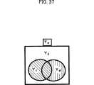
次に、本発明の第2の集積回路装置の動作方法について、図36Bおよび図37により、以下に説明する。
【0246】
図36Bに示すように、あらかじめアドレスが割り当てられている集積回路の集合「Yα」の任意の領域に、アドレスを指定することにより「Yα」の部分集合である「Yβi」((ただし、i=1,2,3,・・・)の第1の集積回路機能形成予定領域を生成する。このようにして、「Yβi」領域が任意の集積回路機能として作用する空間を生成する第1の段階の段階を行う。この第1の集積回路機能形成予定領域は、次式で表される。
【0247】
Yα⊇(Yβ=ΣYβi)(ただし、i=1,2,3,・・・)
【0248】
上記第1の段階の「Yβ」の集積回路機能形成予定領域における部分集合「Yβi」を用いて演算処理および情報処理を行った後に、アドレスを解放する。アドレスの解放は「Yβ」の全集積回路機能形成予定領域でもよいし、もしくは「Yβ」の集積回路領域中の一部の「Yβi」(ただし、i=1,2,3,・・・)に係る集積回路領域でもよい。この段階でアドレスが指定されていない集積回路領域は、図4に示す「Yβ」から解放された集積回路領域「Yτ」、および「Yβ」の補集合の集積回路領域「Yδ」から構成される「Yτ∪Yδ」である。この「Yτ∪Yδ」の集積回路領域に、新たな集積回路機能形成予定領域「Yε」を形成する。「Yε」は複数の集積回路機能形成予定領域から構成される。図36Bに示すように、集積回路領域「Yε」と、「Yβ」から解放されずに残っている「Yφ」(ただし、Yφ⊆Yβ)の集積回路領域とから構成される第2の集積回路機能形成予定領域を生成する。このようにして、「Yε∪Yφ」の集積回路領域が任意の集積回路機能として作用する空間を生成する第2の段階を行う。この第2の集積回路機能形成予定領域は次式で表すことができる。
【0249】
(Yε∪Yφ=ΣYεj⊆Yα)(ただし、j=1,2,3,・・・)
【0250】
ここで「Yε」は、「Yβ」の集積回路領域からアドレス解放されずに残っている領域「Yφ」と独立に、もしくは連携して演算処理を行う。
上記第2の段階の「Yε∪Yφ」の集積回路領域における部分集合「Yεj」を用いて演算処理および情報処理を行った後に、「Yε∪Yφ」を構成する「Yεj」のアドレスを解放する。アドレスの解放は「Yε∪Yφ」の集積回路機能の全集積回路領域でも良いし、もしくは「Yε∪Yφ」の集積回路領域中の一部の「Yλj」(ただし、j=1,2,3,・・・)に係る集積回路機能領域でもよい。
【0251】
次に、「Yε∪Yφ」から解放された集積回路領域と、(Yε∪Yφ)の補集合の集積回路領域「Yη」から構成される集積回路領域「Yξ」と、「Yε∪Yφ」から解放されずに残っている「Yγ」(ただし、Yγ⊆Yε)および「Yρ」の集積回路領域(ただし、Yρ⊆Yβ)から構成される第3の集積回路機能形成予定領域を生成する。このようにして、「Yξ∪Yγ∪Yρ」の集積回路領域が任意の集積回路機能として作用する空間を生成する第3の段階を行う。この第3の集積回路機能形成予定領域は次式で表される。
【0252】
(Yξ∪Yγ∪Yρ=ΣYξm)⊆Yα)(ただし、m=1,2,3,・・・)
【0253】
ここで「Yξ」は、「Yβ」の集積回路領域からアドレス解放されずに残っている集積回路領域「Yφ」および「Yε」の集積回路領域からアドレス解放されずに残っている集積回路領域「Yγ」と独立に、もしくは連携して演算処理を行う。
【0254】
さらに、同様に第4の段階、第5の段階、さらには第nの段階(ただし、n=1,2,3,・・・)とを順に行うことにより、任意の集積回路機能として作用する空間を次々に生成および解放を繰り返すことによって、集積回路の機能を時間分割して使用できる。
【0255】
次に、本発明の第3の集積回路装置の動作方法について、図36Cにより、以下に説明する。
【0256】
図36Cに示すように、あらかじめアドレスが割り当てられている集積回路の集合「YΛ」の任意の集積回路領域に、アドレスを指定することにより「YΛ」の集積回路の部分集合である「YΦi」(ただし、i=1,2,3,・・・)の第1の集積回路機能形成予定領域を生成する。このようにして、「YΦ」の集積回路領域が任意の集積回路機能として作用する空間を生成する第1の段階を行う。この第1の集積回路形成機能形成予定領域は、次式で表される。
【0257】
YΛ⊇(YΦ=ΣYΦi)(ただし、i=1,2,3,・・・)
【0258】
上記第1の段階の「YΦ」の集積回路領域における部分集合「YΦi」を用いて演算処理および情報処理を行った後、「YΦi」(ただし、i=1、2、3、・・・)からなる全集積回路領域である「YΦ」の集積回路機能のアドレスを解放する。
【0259】
次に集積回路機能の設定予定領域にアドレスを指定することにより「YΛ」の中でアドレスを指定された複数の「YΨj」(ただし、j=1,2,3,・・・)の集積回路機能領域を生成する。このようにして、「YΨ」の集積回路領域が任意の集積回路機能として作用する空間を生成する第2の段階が行われる。この集積回路機能領域は、次式で表される。
【0260】
YΛ⊇(YΨ=ΣYΨj)(ただし、j=1,2,3,・・・)
【0261】
上記第2の段階の「YΨ」の集積回路領域における部分集合「YΨj」を用いて演算処理および情報処理を行った後、「YΨj」(ただし、j=1,2,3,・・・)からなる全集積回路領域である「YΨ」の集積回路機能、もしくは「YΨ」の集積回路領域中の、一部の「YΨj」(ただし、j=1,2,3,・・・)に係る集積回路機能のアドレスを解放する。
【0262】
次に、「YΨ」から解放された集積回路領域および「YΨ」の補集合の集積回路領域「YΔ」から構成される集積回路領域「YΘ」と、「YΨ」から解放されずに残っている「YΩ」(ただし、YΩ⊆YΨ)の集積回路領域から構成される集積回路領域を生成する。このようにして、「YΘ∪YΩ」の集積回路領域が任意の集積回路機能として作用する空間を生成する第3の段階が行われる。この集積回路機能領域は、次式で表される。
【0263】
(YΘ∪YΩ=ΣYΥk)⊆YΛ(ただし、k=1,2,3,・・・)
【0264】
上記第3の段階の「YΥ」の集積回路領域における部分集合「YΥk」を用いて演算処理および情報処理を行う。
【0265】
同様に第4の段階、第5の段階をそれぞれ連続にもしくは交互に適宜繰り返し第nの段階(ただし、n=1,2,3,・・・)を行うことにより、任意の集積回路機能として作用する空間を次々に生成および解放を繰り返すことによって、集積回路の機能を時間分割して使用できる。
【0266】
これら第1から第3の集積回路の動作方法は、それぞれ単独に用いてもよいし、あるいは第1から第3の集積回路装置の動作方法と適宜組み合わせて用いても良い。すなわち、時間の経過T1、T2、T3・・・Tmにおいて、任意の経過時間Tq(Tqにおいてさらに分割された時間の経過t0、t1、t2、t3・・・tnが経過している)において、第1から第3の集積回路の任意の動作方法を用いて良い。あるいは、第1の集積回路の動作方法を、第1から第3の集積回路の動作方法と適宜組み合わせて用いても良い。あるいはまた、第2の集積回路の動作方法を、第1から第3の集積回路の動作方法と適宜組み合わせて用いても良い。あるいはまた、第3の集積回路の動作方法、第1から第3の集積回路の動作方法と適宜組み合わせて用いても良い。
【0267】
本発明の第1の集積回路装置は、複数の素子で構成される集積回路装置である。この第1の集積回路装置では、第1の段階で、あらかじめアドレスが割り当てられている素子の集合「A」の任意の領域に、A⊇(Σ=モBi)(ただし、i=1,2,3,・・・)で表される、アドレスを指定することにより「A」の部分集合である「Bi」(ただし、i=1,2,3,・・・)領域を生成し、「B」領域が任意の回路機能として作用する空間を生成する。次に第2の段階で、「Bi」(ただし、i=1,2,3,・・・)の任意の回路機能を使用後に、「Bi」(ただし、i=1,2,3,・・・)の全領域である「B」の回路機能のアドレスを解放し、A⊇(C=ΣCj)(ただし、j=1,2,3,・・・)で表される、「A」の部分集合である「Cj」(ただし、j=1,2,3,・・・)領域を生成し、「C」領域が任意の回路機能として作用する空間を生成する。次に第3の段階で、「Cj」(ただし、j=1,2,3,・・・)の回路機能を使用後に、「Cj」(ただし、j=1,2,3,・・・)の全領域である「C」の回路機能のアドレスを解放し、A⊇(D=ΣDk)(ただし、k=1,2,3,・・・)で表される、「A」の部分集合である「Dk」(ただし、k=1,2,3,・・・)領域を生成し、「D」領域が任意の回路機能として作用する空間を生成する。さらに、同様に第4の段階、第5の段階、さらには第n(ただし、n=1,2,3,・・・)の段階とを行うことにより、任意の回路機能として作用する空間を次々に生成および解放を繰り返すことによって、素子の機能を時間的に分割かつ空間的に分割して機能するものである。
【0268】
本発明の第2の集積回路装置は、複数の素子で構成される集積回路装置である。この第2の集積回路装置は、第1の段階で、あらかじめアドレスが割り当てられている素子の集合「α」の任意の領域に、α⊇(β=Σβi)(ただし、i=1,2,3,・・・)で表されるアドレスを指定することにより「α」の部分集合である「βi」(ただし、i=1,2,3,・・・)領域を生成し、該「β」領域が任意の回路機能として作用する空間を生成する。次に第2の段階で、「βi」(ただし、i=1,2,3,・・・) の任意の回路機能を使用後に、「βi」(ただし、i=1,2,3,・・・)の全領域である「β」の回路機能、もしくは「β」領域中の一部の「βi」(ただし、i=1,2,3,・・・)に係る回路機能のアドレスを解放し、(ε∪φ=Σλj)⊆α(ただし、j=1,2,3,・・・)で表される、「β」から解放された領域および「β」の補集合の領域「δ」から構成される領域「ε」と、「β」から解放されずに残っている「φ」(ただし、φ⊆β)領域とから構成される領域を生成し、「ε∪φ」領域が任意の回路機能として作用する空間を生成する。次に第3の段階で、「λj」(ただし、j=1,2,3,・・・) の回路機能を使用後に、「λj」(ただし、j=1,2,3,・・・)の全領域である「ε∪φ」の回路機能、もしくは「ε∪φ」領域中の一部の「λj」(ただし、j=1,2,3,・・・)に係る回路機能のアドレスを解放し、(ξ∪γ∪ρ=Σζk)⊆α(ただし、k=1,2,3,・・・)で表される、「ε∪φ」から解放された領域と、(ε∪φ)の補集合の領域「η」から構成される領域「ξ」と「ε∪φ」から解放されずに残っている「γ」(ただし、γ⊆ε)および「ρ」(ただし、ρ⊆β)領域から構成される領域を生成し、「ξ∪γ∪ρ」領域が任意の回路機能として作用する空間を生成する。さらに、同様に第4の段階、第5の段階、さらには第n(ただし、n=1,2,3,・・・)の段階とを行うことにより、任意の回路機能として作用する空間を次々に生成および解放を繰り返すことによって、素子の機能を時間的に分割かつ空間的に分割して機能するものである。
【0269】
本発明の第3の集積回路装置は、複数の素子で構成される集積回路装置である。この第3の集積回路装置は、第1の段階で、あらかじめアドレスが割り当てられている素子の集合「Λ」の任意の領域に、Λ⊇(Φ=ΣΦi)(ただし、i=1,2,3,・・・)で表されるアドレスを指定することにより「Λ」の部分集合である「Φi」(ただし、i=1,2,3,・・・)領域を生成し、該「Φ」領域が任意の回路機能として作用する空間を生成する。次に第1の段階で、「Φi」(ただし、i=1,2,3,・・・) の任意の回路機能を使用後に、「Φi」(ただし、i=1,2,3,・・・)の全領域である「Φ」の回路機能のアドレスを解放し、Λ⊇(Ψ=ΣΨj)(ただし、j=1,2,3,・・・)で表される、「Λ」の部分集合である「Ψj」(ただし、j=1,2,3,・・・)領域を生成し、「Ψ」領域が任意の回路機能として作用する空間を生成する。次に第3の段階で、「Ψj」(ただし、j=1,2,3,・・・)の回路機能を使用後に、「Ψj」(ただし、j=1,2,3,・・・)の全領域である「Ψ」の回路機能、もしくは「Ψ」領域中の、一部の「Ψj」(ただし、j=1,2,3,・・・)に係る回路機能のアドレスを解放し、(Θ∪Ω=ΣΥk)⊆Λ(ただし、k=1,2,3,・・・)で表される、「Ψ」から解放された領域および「Ψ」の補集合の領域「Δ」から構成される領域「Θ」と「Ψ」から解放されずに残っている「Ω」(ただし、Ω⊆Ψ)領域とから構成される領域を生成し、「Θ∪Ω」領域が任意の回路機能として作用する空間を生成する。さらに、同様に第2の段階および第3の段階をそれぞれ連続にもしくは交互に適宜繰り返し第nの段階(ただし、n=1,2,3,・・・)とを行うことにより、任意の回路機能として作用する空間を次々に生成および解放を繰り返すことによって、素子の機能を時間的に分割かつ空間的に分割して機能するものである。
【0270】
本発明の第4の集積回路装置は、x個の集積回路を備え、x個の集積回路のうちy番目(1≦y≦x)の集積回路は、同一の集積回路機能もしくは異なった集積回路機能を具備し、かつ各集積回路間でデータもしくは命令、またはデータおよび命令を交換する集積回路装置である。この第4の集積回路装置は、第1の段階で、あらかじめ個々の集積回路にアドレスが割り当てられている集積回路の集合「YA」の任意の集積回路に、(YB=ΣYBi)⊆YA(ただし、i=1,2,3,・・・)で表されるアドレスを指定することにより「YA」の部分集合である「YBi」(ただし、i=1,2,3,・・・)となる集積回路の集合を生成し、「YB」なる集積回路の集合が任意の機能を発現する空間を生成する。次に第2の段階で、「YBi」(ただし、i=1,2,3,・・・)の任意の集積回路機能を使用後に、「YBi」(ただし、i=1,2,3,・・・)の全集積回路の集合である「YB」のアドレスを解放し、(YC=ΣYCj)⊆YA(ただし、j=1,2,3,・・・)で表される「YA」の部分集合である「YCj」(ただし、j=1,2,3,・・・)なる集積回路の集合を生成し、該「YC」なる集積回路の集合が任意の集積回路機能を発現する空間を生成する。次に第3の段階で、「YCj」(ただし、j=1,2,3,・・・)の集積回路機能を使用後に、「YCj」(ただし、j=1,2,3,・・・)の全集積回路の集合である「YC」のアドレスを解放し、(YD=ΣYDk)⊆A(ただし、k=1,2,3,・・・)で表される「YA」の部分集合である「YDk」(ただし、k=1,2,3,・・・)なる集積回路の集合を生成し、該「YD」なる集積回路の集合が任意の集積回路機能を発現する空間を生成する。さらに、同様に第4の段階、第5の段階、さらには第n回(ただし、n=1,2,3,・・・)の段階とを順に行うことにより、任意の集積回路の機能を発現する空間を次々に生成および解放を繰り返すことによって、集積回路の機能を時間的に分割かつ空間的に分割して使用するものである。
【0271】
加えて上記集積回路は、複数の素子で構成され、第1の段階で、あらかじめアドレスが割り当てられている前記集積回路の素子の集合「A」の任意の領域に、A⊇(B=ΣBi)(ただし、i=1,2,3,・・・)で表されるアドレスを指定することにより「A」の部分集合である「Bi」(ただし、i=1,2,3,・・・)領域を生成し、「B」領域が任意の回路機能として作用する空間を生成する。次に第2の段階で、「Bi」(ただし、i=1,2,3,・・・)の任意の回路機能を使用後に、「Bi」(ただし、i=1,2,3,・・・)の全領域である「B」の回路機能のアドレスを解放し、A⊇(C=ΣCj)(ただし、j=1,2,3,・・・)で表される「A」の部分集合である「Cj」(ただし、j=1,2,3,・・・)領域を生成し、該「C」領域が任意の回路機能として作用する空間を生成する。次に第3の段階で、「Cj」(ただし、j=1,2,3,・・・)の回路機能を使用後に、「Cj」(ただし、j=1,2,3,・・・)の全領域である「C」の回路機能のアドレスを解放し、A⊇(D=ΣDk)(ただし、k=1,2,3,・・・)で表される「A」の部分集合である「Dk」(ただし、k=1,2,3,・・・)領域を生成し、「D」領域が任意の回路機能として作用する空間を生成する。さらに、同様に第4の段階、第5の段階、さらには第nの段階(ただし、n=1,2,3,・・・)とを順に行うことにより、任意の回路機能として作用する空間を次々に生成および解放を繰り返すことによって、素子の機能を時間的に分割かつ空間的に分割して使用するものである。
【0272】
本発明の第5の集積回路装置は、x個の集積回路を備えている。このx個の集積回路のうちy番目(1≦y≦x)の集積回路は、第1の段階で、あらかじめ個々の集積回路にアドレスが割り当てられている集積回路の集合「Yα」の任意の集積回路に、(Yβ=ΣYβi)⊆Yα(ただし、i=1,2,3,・・・)で表されるアドレスを指定することにより「Yα」の部分集合である「Yβi」(ただし、i=1,2,3,・・・)となる集積回路の集合を生成し、「Yβ」なる集積回路の集合が任意の集積回路機能を発現する空間を生成する。次に第2の段階で、「Yβi」(ただし、i=1,2,3,・・・)の任意の集積回路機能を使用後に、「Yβi」(ただし、i=1,2,3,・・・)の全集積回路の集合である「Yβ」の集積回路機能のアドレス、もしくは「Yβ」の集積回路の集合中一部の「Yβi」(ただし、i=1,2,3,・・・)に係る集積回路機能のアドレスを解放し、(Yε∪Yφ=ΣYλj)⊆Yα(ただし、j=1,2,3,・・・)で表される「Yβ」から解放される集積回路の集合および「Yβ」の補集合「Yδ」から構成される「Yε」なる集積回路の集合と、「Yβ」から解放されずに残っている集積回路の集合「Yφ」(Yφ⊆Yβ)から構成される集積回路の集合とを生成し、「Yε∪Yφ」なる集積回路の集合が任意の集積回路機能を発現する空間を生成する。次に第3の段階で、「Yλj」(ただし、j=1,2,3,・・・)の集積回路機能を使用後に、「Yλj」(ただし、j=1,2,3,・・・)の全集積回路の集合である「Yε∪Yφ」に係る集積回路機能のアドレス、もしくは「Yε∪Yφ」なる集積回路の集合中一部の「Yλj」(ただし、j=1,2,3,・・・)に係る集積回路機能のアドレスを解放し、(Yξ∪Yγ∪Yρ=ΣYζk)⊆Yα(ただし、k=1,2,3,・・・)で表される「Yε∪Yφ」から解放された集積回路の集合と、「Yε∪Yφ」の補集合「Yη」から構成される「Yξ」なる集積回路の集合と、「Yε∪Yφ」から解放されずに残っている「Yγ」(Yγ⊆Yε)および「Yρ」(Yρ⊆Yβ)領域から構成される集積回路の集合を生成し、「Yξ∪Yγ∪Yρ」なる集積回路の集合が任意の集積回路の機能として作用する空間を生成する。さらに、同様に第4の段階、第5の段階、さらには第n回(ただし、n=1,2,3,・・・)の段階とを順に行うことにより、任意の集積回路の機能を発現する空間を次々に生成および解放を繰り返すことによって、集積回路の機能を時間的に分割かつ空間的に分割して使用されるものである。
【0273】
加えて上記集積回路は、複数の素子で構成され、第1の段階で、あらかじめアドレスが割り当てられている前記集積回路の素子の集合「A」の任意の領域に、A⊇(B=ΣBi)(ただし、i=1,2,3,・・・)で表されるアドレスを指定することにより「A」の部分集合である「Bi」(ただし、i=1,2,3,・・・)領域、「B」領域が任意の回路機能として作用する空間を生成する。次に第2の段階で、「Bi」(ただし、i=1,2,3,・・・)の任意の回路機能を使用後に、「Bi」(ただし、i=1,2,3,・・・)の全領域である「B」の回路機能のアドレスを解放し、A⊇(C=ΣCj)(ただし、j=1,2,3,・・・)で表される「A」の部分集合である「Cj」(ただし、j=1,2,3,・・・)領域を生成し、「C」領域が任意の回路機能として作用する空間を生成する。次に第3の段階で、「Cj」(ただし、j=1,2,3,・・・)の回路機能を使用後に、「Cj」(ただし、j=1,2,3,・・・)の全領域である「C」の回路機能のアドレスを解放し、A⊇(D=ΣDk)(ただし、k=1,2,3,・・・)で表される「A」の部分集合である「Dk」(ただし、k=1,2,3,・・・)領域を生成し、「D」領域が任意の回路機能として作用する空間を生成する。さらに、同様に第4の段階、第5の段階、さらには第nの段階(ただし、n=1,2,3,・・・)とを順に行うことにより、任意の回路機能として作用する空間を次々に生成および解放を繰り返すことによって、素子の機能を時間的に分割かつ空間的に分割して使用するも
のである。
【0274】
本発明の第6の集積回路装置は、x個の集積回路を備えている。このx個の集積回路のうちy番目(1≦y≦x)の集積回路は、第1の段階で、あらかじめ個々の集積回路にアドレスが割り当てられている集積回路の集合「YΛ」の任意の集積回路に、(YΦ=ΣYΦi)⊆YΛ(ただし、i=1,2,3,・・・)で表されるアドレスを指定することにより「YΛ」の部分集合である「YΦi」(ただし、i=1,2,3,・・・)の集積回路の集合を生成し、「YΦ」の集積回路の集合が任意の機能を発現する空間を生成する。次に第2の段階で、「YΦi」(ただし、i=1,2,3,・・・)の任意の集積回路機能を使用後に、「YΦi」(ただし、i=1,2,3,・・・)の全集積回路の集合である「YΦ」の集積回路機能のアドレスを解放し、(YΨ=ΣYΨj)⊆YΛ(ただし、j=1,2,3,・・・)で表される「YΛ」の部分集合である「YΨj」(ただし、j=1,2,3,・・・)の集積回路の集合を生成し、「YΨ」の集積回路の集合が任意の集積回路機能を発現する空間を生成する。次に第3の段階で、「YΨj」(ただし、j=1,2,3,・・・)の集積回路機能を使用後に、「YΨj」(ただし、j=1,2,3,・・・)の全集積回路の集合である「YΨ」の集積回路機能のアドレス、もしくは「YΨ」領域中の一部の「YΨj」(ただし、j=1,2,3,・・・)に係る機能のアドレスを解放し、(YΘ∪YΩ=ΣYΥk)⊆YΛ(ただし、k=1,2,3,・・・)で表される、「YΨ」から解放された集積回路の集合および「YΨ」の補集合「YΔ」から構成される集積回路の集合「YΘ」と「YΨ」から解放されずに残っている「YΩ」(YΩ⊆YΨ)の集積回路の集合を生成し、「YΘ∪YΩ」なる集積回路の集合が任意の機能を発現する空間を生成する。さらに、同様に第4の段階、第5の段階、さらには第n回(ただし、n=1,2,3,・・・)の段階とを順に行うことにより、任意の集積回路の機能を発現する空間を次々に生成および解放を繰り返すことによって、集積回路の機能を時間的に分割かつ空間的に分割して使用するものである。
【0275】
加えて、上記集積回路は、複数の素子で構成され、第1の段階で、あらかじめアドレスが割り当てられている前記集積回路の素子の集合「A」の任意の領域に、A⊇(B=ΣBi)(ただし、i=1,2,3,・・・)で表されるアドレスを指定することにより「A」の部分集合である「Bi」(ただし、i=1,2,3,・・・)領域、「B」領域が任意の回路機能として作用する空間を生成する。次に第2の段階で、「Bi」(ただし、i=1,2,3,・・・)の任意の回路機能を使用後に、「Bi」(ただし、i=1,2,3,・・・)の全領域である「B」の回路機能のアドレスを解放し、A⊇(C=ΣCj)(ただし、j=1,2,3,・・・)で表される「A」の部分集合である「Cj」(ただし、j=1,2,3,・・・)領域を生成し、「C」領域が任意の回路機能として作用する空間を生成する。次に第3の段階で、「Cj」(ただし、j=1,2,3,・・・)の回路機能を使用後に、「Cj」(ただし、j=1,2,3,・・・)の全領域である「C」の回路機能のアドレスを解放し、A⊇(D=ΣDk)(ただし、k=1,2,3,・・・)で表される「A」の部分集合である「Dk」(ただし、k=1,2,3,・・・)領域を生成し、「D」領域が任意の回路機能として作用する空間を生成する。さらに、同様に第4の段階、第5の段階、さらには第nの段階(ただし、n=1,2,3,・・・)とを順に行うことにより、任意の回路機能として作用する空間を次々に生成および解放を繰り返すことによって、素子の機能を時間的に分割かつ空間的に分割して使用するものである。
【0276】
本発明の第7の集積回路装置は、x個の集積回路を備え、x個の集積回路のうちy番目(1≦y≦x)の集積回路は、同一の集積回路機能もしくは異なった集積回路機能を具備し、かつ各集積回路間でデータもしくは命令、またはデータおよび命令を交換する集積回路装置である。この第7の集積回路装置は、第1の段階で、あらかじめ個々の集積回路にアドレスが割り当てられている集積回路の集合「YA」の任意の集積回路に、(YB=ΣYBi)⊆YA(ただし、i=1,2,3,・・・)で表されるアドレスを指定することにより「YA」の部分集合である「YBi」(ただし、i=1,2,3,・・・)となる集積回路の集合を生成し、「YB」なる集積回路の集合が任意の機能を発現する空間を生成する。次に第2の段階で、「YBi」(ただし、i=1,2,3,・・・)の任意の集積回路機能を使用後に、「YBi」(ただし、i=1,2,3,・・・)の全集積回路の集合である「YB」のアドレスを解放し、(YC=ΣYCj)⊆YA(ただし、j=1,2,3,・・・)で表される「YA」の部分集合である「YCj」(ただし、j=1,2,3,・・・)なる集積回路の集合を生成し、該「YC」なる集積回路の集合が任意の集積回路機能を発現する空間を生成する。次に第3の段階で、「YCj」(ただし、j=1,2,3,・・・)の集積回路機能を使用後に、「YCj」(ただし、j=1,2,3,・・・)の全集積回路の集合である「YC」のアドレスを解放し、(YD=ΣYDk)⊆A(ただし、k=1,2,3,・・・)で表される「YA」の部分集合である「YDk」(ただし、k=1,2,3,・・・)なる集積回路の集合を生成し、該「YD」なる集積回路の集合が任意の集積回路機能を発現する空間を生成する。さらに、同様に第4の段階、第5の段階、さらには第n回(ただし、n=1,2,3,・・・)の段階とを順に行うことにより、任意の集積回路の機能を発現する空間を次々に生成および解放を繰り返すことによって、集積回路の機能を時間的に分割かつ空間的に分割して使用されるものである。
【0277】
加えて、上記集積回路は、複数の素子で構成され、第1の段階で、あらかじめアドレスが割り当てられている前記集積回路の素子の集合「α」の任意の領域に、(β=Σβi)⊆α(ただし、i=1,2,3,・・・)で表されるアドレスを指定することにより「α」の部分集合である「βi」(ただし、i=1,2,3,・・・)領域を生成し、「β」領域が任意の回路機能として作用する空間を生成する。次に第2の段階で、「βi」(ただし、i=1,2,3,・・・)領域の任意の回路機能を使用後に、「βi」(ただし、i=1,2,3,・・・)の全領域である「β」領域の回路機能、もしくは「β」領域中の一部の「βi」(ただし、i=1,2,3,・・・)に係る回路機能のアドレスを解放し、(ε∪φ=Σλj)⊆α(ただし、j=1,2,3,・・・)で表される、「β」から解放された領域および「β」の補集合の「δ」領域から構成される「ε」領域と、「β」から解放されずに残っている「φ」(φ⊆β)領域とから構成される領域を生成し、「ε∪φ」領域が任意の回路機能として作用する空間を生成する。次に第3の段階で、「λj」(ただし、j=1,2,3,・・・)の回路機能を使用後に、「λj」(ただし、j=1,2,3,・・・)の全領域である「ε∪φ」の回路機能、もしくは「ε∪φ」領域中の一部の「λj」(ただし、j=1,2,3,・・・)に係る回路機能のアドレスを解放し、(ξ∪γ∪ρ=Σζk)⊆α(ただし、k=1,2,3,・・・)で表される、「ε∪φ」から解放された領域と、(ε∪φ)の補集合の「η」領域から構成される「ξ」領域と、「ε∪φ」から解放されずに残っている「γ」(ただし、γ⊆ε)領域と、「ρ」(ただし、ρ⊆β)領域とから構成される領域を生成し、「ξ∪γ∪ρ」領域が任意の回路機能として作用する空間を生成する。さらに、同様に第4の段階、第5の段階、さらには第nの段階(ただし、n=1,2,3,・・・)とを順に行うことにより、任意の回路機能として作用する空間を次々に生成および解放を繰り返すことによって、素子の機能を時間的に分割かつ空間的に分割して使用するものである。
【0278】
本発明の第8の集積回路装置は、x個の集積回路を備えている。このx個の集積回路のうちy番目(1≦y≦x)の集積回路は、第1の段階で、あらかじめ個々の集積回路にアドレスが割り当てられている集積回路の集合「Yα」の任意の集積回路に、(Yβ=ΣYβi)⊆Yα(ただし、i=1,2,3,・・・)で表されるアドレスを指定することにより「Yα」の部分集合である「Yβi」(ただし、i=1,2,3,・・・)なる集積回路の集合を生成し、「Yβ」なる集積回路の集合が任意の機能を発現する空間を生成する。次に第2の段階で、「Yβi」(ただし、i=1,2,3,・・・)の任意の集積回路機能を使用後に、「Yβi」(ただし、i=1,2,3,・・・)の全集積回路の集合である「Yβ」の集積回路機能のアドレス、もしくは「Yβ」の集積回路の集合中一部の「Yβi」(ただし、i=1,2,3,・・・)に係る集積回路機能のアドレスを解放し、(Yε∪Yφ=ΣYλj)⊆Yα(ただし、j=1,2,3,・・・)で表される「Yβ」から解放された集積回路の集合および「Yβ」の補集合「Yδ」から構成される「Yε」なる集積回路の集合と、「Yβ」から解放されずに残っている「Yφ」(ただし、Yφ⊆Yβ)の集積回路の集合から構成される集積回路の集合を生成し、「Yε∪Yφ」の集積回路の集合が任意の集積回路機能を発現する空間を生成する。次に第3の段階で、「Yλj」(ただし、j=1,2,3,・・・)の集積回路機能を使用後に、「Yλj」(ただし、j=1,2,3,・・・)の全集積回路の集合である「Yε∪Yφ」に係る集積回路機能のアドレス、もしくは「Yε∪Yφ」なる集積回路の集合中一部の「Yλj」(ただし、j=1,2,3,・・・)に係る集積回路機能のアドレスを解放し、(Yξ∪Yγ∪Yρ=ΣYζk)⊆Yα(ただし、k=1,2,3,・・・)で表される「Yε∪Yφ」から解放された集積回路の集合と、「Yε∪Yφ」の補集合「Yη」から構成される「Yξ」なる集積回路の集合と、「Yε∪Yφ」から解放されずに残っている「Yγ」(ただし、Yγ⊆Yε)および「Yρ」(ただし、Yρ⊆Yβ)なる集積回路の集合を生成し、「Yξ∪Yγ∪Yρ」の集積回路の集合が任意の集積回路の機能として作用する空間を生成する。さらに、同様に第4の段階、第5の段階、さらには第n回(ただし、n=1,2,3,・・・)の段階を順に行うことにより、任意の集積回路の機能を発現する空間を次々に生成および解放を繰り返すことによって、集積回路の機能を時間的に分割かつ空間的に分割して使用されるものである。
【0279】
加えて、上記集積回路は、複数の素子で構成され、第1の段階で、あらかじめアドレスが割り当てられている前記集積回路の素子の集合「α」の任意の領域に、(β=Σβi)⊆α(ただし、i=1,2,3,・・・)で表されるアドレスを指定することにより「α」の部分集合である「βi」(ただし、i=1,2,3,・・・)領域を生成し、「β」領域が任意の回路機能として作用する空間を生成する。次に第2の段階で、「βi」(ただし、i=1,2,3,・・・)領域の任意の回路機能を使用後に、「βi」(ただし、i=1,2,3,・・・)の全領域である「β」領域の回路機能、もしくは「β」領域中の一部の「βi」(ただし、i=1,2,3,・・・)に係る回路機能のアドレスを解放し、(ε∪φ=Σλj)⊆α(ただし、j=1,2,3,・・・)で表される、「β」から解放された領域および「β」の補集合の「δ」領域から構成される「ε」領域と、「β」から解放されずに残っている「φ」(φ⊆β)領域とから構成される領域を生成し、「ε∪φ」領域が任意の回路機能として作用する空間を生成する。次に第3の段階で、「λj」(ただし、j=1,2,3,・・・)の回路機能を使用後に、「λj」(ただし、j=1,2,3,・・・)の全領域である「ε∪φ」の回路機能、もしくは「ε∪φ」領域中の一部の「λj」(ただし、j=1,2,3,・・・)に係る回路機能のアドレスを解放し、(ξ∪γ∪ρ=Σζk)⊆α(ただし、k=1,2,3,・・・)で表される、「ε∪φ」から解放された領域と、(ε∪φ)の補集合の「η」領域から構成される「ξ」領域と、「ε∪φ」から解放されずに残っている「γ」(ただし、γ⊆ε)領域と、「ρ」(ただし、ρ⊆β)領域とから構成される領域を生成し、「ξ∪γ∪ρ」領域が任意の回路機能として作用する空間を生成する。さらに、同様に第4の段階、第5の段階、さらには第nの段階(ただし、n=1,2,3,・・・)とを順に行うことにより、任意の回路機能として作用する空間を次々に生成および解放を繰り返すことによって、素子の機能を時間的に分割かつ空間的に分割して使用するものである。
【0280】
本発明の第9の集積回路装置は、x個の集積回路を備えている。このx個の集積回路のうちy番目(1≦y≦x)の集積回路は、第1の段階で、あらかじめ個々の集積回路にアドレスが割り当てられている集積回路の集合「YΛ」の任意の集積回路に、(YΦ=ΣYΦi)⊆YΛ(ただし、i=1,2,3,・・・)で表されるアドレスを指定することにより「YΛ」の部分集合である「YΦi」(ただし、i=1,2,3,・・・)の集積回路の集合を生成し、「YΦ」の集積回路の集合が任意の機能を発現する空間を生成する。次に第2の段階で、「YΦi」(ただし、i=1,2,3,・・・)の任意の集積回路機能を使用後に、「YΦi」(ただし、i=1,2,3,・・・)の全集積回路の集合である「YΦ」の集積回路機能のアドレスを解放し、(YΨ=ΣYΨj)⊆YΛ(ただし、j=1,2,3,・・・)で表される「YΛ」の部分集合である「YΨj」(ただし、j=1,2,3,・・・)の集積回路の集合を生成し、「YΨ」の集積回路の集合が任意の集積回路機能を発現する空間を生成する。次に第3の段階で、「YΨj」(ただし、j=1,2,3,・・・)の集積回路機能を使用後に、「YΨj」(ただし、j=1,2,3,・・・)の全集積回路の集合である「YΨ」の集積回路機能のアドレス、もしくは「YΨ」領域中の一部の「YΨj」(ただし、j=1,2,3,・・・)に係る機能のアドレスを解放し、(YΘ∪YΩ=ΣYΥk)⊆YΛ(ただし、k=1,2,3,・・・)で表される、「YΨ」から解放された集積回路の集合および「YΨ」の補集合「YΔ」から構成される集積回路の集合「YΘ」と「YΨ」から解放されずに残っている「YΩ」(YΩ⊆YΨ)の集積回路の集合を生成し、「YΘ∪YΩ」なる集積回路の集合が任意の機能を発現する空間を生成する。さらに、同様に第4の段階、第5の段階、さらには第n回(ただし、n=1,2,3,・・・)の段階とを順に行うことにより、任意の集積回路の機能を発現する空間を次々に生成および解放を繰り返すことによって、集積回路の機能を時間的に分割かつ空間的に分割して使用されるものである。
【0281】
加えて、上記集積回路は、複数の素子で構成され、第1の段階で、あらかじめアドレスが割り当てられている前記集積回路の素子の集合「α」の任意の領域に、(β=Σβi)⊆α(ただし、i=1,2,3,・・・)で表されるアドレスを指定することにより「α」の部分集合である「βi」(ただし、i=1,2,3,・・・)領域を生成し、「β」領域が任意の回路機能として作用する空間を生成する。次に第2の段階で、「βi」(ただし、i=1,2,3,・・・)領域の任意の回路機能を使用後に、「βi」(ただし、i=1,2,3,・・・)の全領域である「β」領域の回路機能、もしくは「β」領域中の一部の「βi」(ただし、i=1,2,3,・・・)に係る回路機能のアドレスを解放し、(ε∪φ=Σλj)⊆α(ただし、j=1,2,3,・・・)で表される、「β」から解放された領域および「β」の補集合の「δ」領域から構成される「ε」領域と、「β」から解放されずに残っている「φ」(φ⊆β)領域とから構成される領域を生成し、「ε∪φ」領域が任意の回路機能として作用する空間を生成する。次に第3の段階で、「λj」(ただし、j=1,2,3,・・・)の回路機能を使用後に、「λj」(ただし、j=1,2,3,・・・)の全領域である「ε∪φ」の回路機能、もしくは「ε∪φ」領域中の一部の「λj」(ただし、j=1,2,3,・・・)に係る回路機能のアドレスを解放し、(ξ∪γ∪ρ=Σζk)⊆α(ただし、k=1,2,3,・・・)で表される、「ε∪φ」から解放された領域と、(ε∪φ)の補集合の「η」領域から構成される「ξ」領域と、「ε∪φ」から解放されずに残っている「γ」(ただし、γ⊆ε)領域と、「ρ」(ただし、ρ⊆β)領域とから構成される領域を生成し、「ξ∪γ∪ρ」領域が任意の回路機能として作用する空間を生成する。さらに、同様に第4の段階、第5の段階、さらには第nの段階(ただし、n=1,2,3,・・・)とを順に行うことにより、任意の回路機能として作用する空間を次々に生成および解放を繰り返すことによって、素子の機能を時間的に分割かつ空間的に分割して使用するものである。
【0282】
本発明の第10の集積回路装置は、x個の集積回路を備え、x個の集積回路のうちy番目(1≦y≦x)の集積回路は、同一の集積回路機能もしくは異なった集積回路機能を具備し、かつ各集積回路間でデータもしくは命令、またはデータおよび命令を交換する集積回路装置である。この第10の集積回路装置は、第1の段階で、あらかじめ個々の集積回路にアドレスが割り当てられている集積回路の集合「YA」の任意の集積回路に、(YB=ΣYBi)⊆YA(ただし、i=1,2,3,・・・)で表されるアドレスを指定することにより「YA」の部分集合である「YBi」(ただし、i=1,2,3,・・・)となる集積回路の集合を生成し、「YB」なる集積回路の集合が任意の機能を発現する空間を生成する。
次に第2の段階で、「YBi」(ただし、i=1,2,3,・・・)の任意の集積回路機能を使用後に、「YBi」(ただし、i=1,2,3,・・・)の全集積回路の集合である「YB」のアドレスを解放し、(YC=ΣYCj)⊆YA(ただし、j=1,2,3,・・・)で表される「YA」の部分集合である「YCj」(ただし、j=1,2,3,・・・)なる集積回路の集合を生成し、該「YC」なる集積回路の集合が任意の集積回路機能を発現する空間を生成する。次に第3の段階で、「YCj」(ただし、j=1,2,3,・・・)の集積回路機能を使用後に、「YCj」(ただし、j=1,2,3,・・・)の全集積回路の集合である「YC」のアドレスを解放し、(YD=ΣYDk)⊆A(ただし、k=1,2,3,・・・)で表される「YA」の部分集合である「YDk」(ただし、k=1,2,3,・・・)なる集積回路の集合を生成し、該「YD」なる集積回路の集合が任意の集積回路機能を発現する空間を生成する。さらに、同様に第4の段階、第5の段階、さらには第n回(ただし、n=1,2,3,・・・)の段階とを順に行うことにより、任意の集積回路の機能を発現する空間を次々に生成および解放を繰り返すことによって、集積回路の機能を時間的に分割かつ空間的に分割して使用するものである。
【0283】
加えて、上記集積回路は、複数の素子で構成され、第1の段階で、あらかじめアドレスが割り当てられている前記集積回路の素子の集合「Λ」の任意の領域に、Λ⊇(Φ=ΣΦi)(ただし、i=1,2,3,・・・)で表されるアドレスを指定することにより「Λ」の部分集合である「Φi」(ただし、i=1,2,3,・・・)領域を生成し、「Φ」領域が任意の回路機能として作用する空間を生成する。次に第2の段階で、「Φi」(ただし、i=1,2,3,・・・)の任意の回路機能を使用後に、「Φi」(ただし、i=1,2,3,・・・)の全領域である「Φ」の回路機能のアドレスを解放し、Λ⊇(Ψ=ΣΨj)(ただし、j=1,2,3,・・・)で表される「Λ」の部分集合である「Ψj」(ただし、j=1,2,3,・・・)領域を生成し、「Ψ」領域が任意の回路機能として作用する空間を生成する第2の段階と、
「Ψj」(ただし、j=1,2,3,・・・)の回路機能を使用後に、「Ψj」(ただし、j=1,2,3,・・・)の全領域である「Ψ」の回路機能、もしくは「Ψ」領域中の一部の「Ψj」(ただし、j=1,2,3,・・・)に係る回路機能のアドレスを解放し、(Θ∪Ω=ΣΥk)⊆Λ(ただし、k=1,2,3,・・・)で表される、「Ψ」から解放された領域および「Ψ」の補集合の領域「Δ」から構成される領域「Θ」と「Ψ」から解放されずに残っている「Ω」(Ω⊆Ψ)領域から構成される領域を生成し、「Θ∪Ω」領域が任意の回路機能として作用する空間を生成する。同様に第2の段階および第3の段階をそれぞれ連続にもしくは交互に適宜繰り返し第nの段階(ただし、n=1,2,3,・・・)とを行うことにより、任意の回路機能として作用する空間を次々に生成および解放を繰り返すことによって、素子の機能を時間的に分割かつ空間的に分割して使用するものである。
【0284】
本発明の第11の集積回路装置は、x個の集積回路を備えている。このx個の集積回路のうちy番目(1≦y≦x)の集積回路は、第1の段階で、あらかじめ個々の集積回路にアドレスが割り当てられている集積回路の集合「Yα」の任意の集積回路に、(Yβ=ΣYβi)⊆Yα(ただし、i=1,2,3,・・・)で表されるアドレスを指定することにより「Yα」の部分集合である「Yβi」(ただし、i=1,2,3,・・・)なる集積回路の集合を生成し、「Yβ」なる集積回路の集合が任意の機能を発現する空間を生成する。次に第2の段階で、「Yβi」(ただし、i=1,2,3,・・・)の任意の集積回路機能を使用後に、「Yβi」(ただし、i=1,2,3,・・・)の全集積回路の集合である「Yβ」の集積回路機能のアドレス、もしくは「Yβ」の集積回路の集合中一部の「Yβi」(ただし、i=1,2,3,・・・)に係る集積回路機能のアドレスを解放し、(Yε∪Yφ=ΣYλj)⊆Yα(ただし、j=1,2,3,・・・)で表される「Yβ」から解放された集積回路の集合および「Yβ」の補集合「Yδ」から構成される「Yε」なる集積回路の集合と、「Yβ」から解放されずに残っている「Yφ」(ただし、Yφ⊆Yβ)の集積回路の集合から構成される集積回路の集合を生成し、「Yε∪Yφ」の集積回路の集合が任意の集積回路機能を発現する空間を生成する。次に第3の段階で、「Yλj」(ただし、j=1,2,3,・・・)の集積回路機能を使用後に、「Yλj」(ただし、j=1,2,3,・・・)の全集積回路の集合である「Yε∪Yφ」に係る集積回路機能のアドレス、もしくは「Yε∪Yφ」なる集積回路の集合中一部の「Yλj」(ただし、j=1,2,3,・・・)に係る集積回路機能のアドレスを解放し、(Yξ∪Yγ∪Yρ=ΣYζk)⊆Yα(ただし、k=1,2,3,・・・)で表される「Yε∪Yφ」から解放された集積回路の集合と、「Yε∪Yφ」の補集合「Yη」から構成される「Yξ」なる集積回路の集合と、「Yε∪Yφ」から解放されずに残っている「Yγ」(ただし、Yγ⊆Yε)および「Yρ」(ただし、Yρ⊆Yβ)なる集積回路の集合を生成し、「Yξ∪Yγ∪Yρ」の集積回路の集合が任意の集積回路の機能として作用する空間を生成する。さらに、同様に第4の段階、第5の段階、さらには第n回(ただし、n=1,2,3,・・・)の段階を順に行うことにより、任意の集積回路の機能を発現する空間を次々に生成および解放を繰り返すことによって、集積回路の機能を時間的に分割かつ空間的に分割して使用するものである。
【0285】
加えて、上記集積回路は、複数の素子で構成され、第1の段階で、あらかじめアドレスが割り当てられている前記集積回路の素子の集合「Λ」の任意の領域に、Λ⊇(Φ=ΣΦi)(ただし、i=1,2,3,・・・)で表されるアドレスを指定することにより「Λ」の部分集合である「Φi」(ただし、i=1,2,3,・・・)領域を生成し、「Φ」領域が任意の回路機能として作用する空間を生成する。次に第2の段階で、「Φi」(ただし、i=1,2,3,・・・)の任意の回路機能を使用後に、「Φi」(ただし、i=1,2,3,・・・)の全領域である「Φ」の回路機能のアドレスを解放し、Λ⊇(Ψ=ΣΨj)(ただし、j=1,2,3,・・・)で表される「Λ」の部分集合である「Ψj」(ただし、j=1,2,3,・・・)領域を生成し、「Ψ」領域が任意の回路機能として作用する空間を生成する。次に第3の段階で、「Ψj」(ただし、j=1,2,3,・・・)の回路機能を使用後に、「Ψj」(ただし、j=1,2,3,・・・)の全領域である「Ψ」の回路機能、もしくは「Ψ」領域中の一部の「Ψj」(ただし、j=1,2,3,・・・)に係る回路機能のアドレスを解放し、(Θ∪Ω=ΣΥk)⊆Λ(ただし、k=1,2,3,・・・)で表される、「Ψ」から解放された領域および「Ψ」の補集合の領域「Δ」から構成される領域「Θ」と「Ψ」から解放されずに残っている「Ω」(Ω⊆Ψ)領域から構成される領域を生成し、「Θ∪Ω」領域が任意の回路機能として作用する空間を生成する。同様に第2の段階および第3の段階をそれぞれ連続にもしくは交互に適宜繰り返し第nの段階(ただし、n=1,2,3,・・・)とを行うことにより、任意の回路機能として作用する空間を次々に生成および解放を繰り返すことによって、素子の機能を時間的に分割かつ空間的に分割して使用するものである。
【0286】
本発明の第12の集積回路装置は、x個の集積回路を備えている。このx個の集積回路のうちy番目(1≦y≦x)の集積回路は、第1の段階で、あらかじめ個々の集積回路にアドレスが割り当てられている集積回路の集合「YΛ」の任意の集積回路に、(YΦ=ΣYΦi)⊆YΛ(ただし、i=1,2,3,・・・)で表されるアドレスを指定することにより「YΛ」の部分集合である「YΦi」(ただし、i=1,2,3,・・・)の集積回路の集合を生成し、「YΦ」の集積回路の集合が任意の機能を発現する空間を生成する。次に第2の段階で、「YΦi」(ただし、i=1,2,3,・・・)の任意の集積回路機能を使用後に、「YΦi」(ただし、i=1,2,3,・・・)の全集積回路の集合である「YΦ」の集積回路機能のアドレスを解放し、(YΨ=ΣYΨj)⊆YΛ(ただし、j=1,2,3,・・・)で表される「YΛ」の部分集合である「YΨj」(ただし、j=1,2,3,・・・)の集積回路の集合を生成し、「YΨ」の集積回路の集合が任意の集積回路機能を発現する空間を生成する。次に第3の段階で、「YΨj」(ただし、j=1,2,3,・・・)の集積回路機能を使用後に、「YΨj」(ただし、j=1,2,3,・・・)の全集積回路の集合である「YΨ」の集積回路機能のアドレス、もしくは「YΨ」領域中の一部の「YΨj」(ただし、j=1,2,3,・・・)に係る機能のアドレスを解放し、(YΘ∪YΩ=ΣYΥk)⊆YΛ(ただし、k=1,2,3,・・・)で表される、「YΨ」から解放された集積回路の集合および「YΨ」の補集合「YΔ」から構成される集積回路の集合「YΘ」と「YΨ」から解放されずに残っている「YΩ」(YΩ⊆YΨ)の集積回路の集合を生成し、「YΘ∪YΩ」なる集積回路の集合が任意の機能を発現する空間を生成する。さらに、同様に第4の段階、第5の段階、さらには第n回(ただし、n=1,2,3,・・・)の段階とを順に行うことにより、任意の集積回路の機能を発現する空間を次々に生成および解放を繰り返すことによって、集積回路の機能を時間的に分割かつ空間的に分割して使用するものである。
【0287】
加えて、上記集積回路は、複数の素子で構成され、第1の段階で、あらかじめアドレスが割り当てられている前記集積回路の素子の集合「Λ」の任意の領域に、Λ⊇(Φ=ΣΦi)(ただし、i=1,2,3,・・・)で表されるアドレスを指定することにより「Λ」の部分集合である「Φi」(ただし、i=1,2,3,・・・)領域を生成し、「Φ」領域が任意の回路機能として作用する空間を生成する。次に第2の段階で、「Φi」(ただし、i=1,2,3,・・・)の任意の回路機能を使用後に、「Φi」(ただし、i=1,2,3,・・・)の全領域である「Φ」の回路機能のアドレスを解放し、Λ⊇(Ψ=ΣΨj)(ただし、j=1,2,3,・・・)で表される「Λ」の部分集合である「Ψj」(ただし、j=1,2,3,・・・)領域を生成し、「Ψ」領域が任意の回路機能として作用する空間を生成する。次に第3の段階で、「Ψj」(ただし、j=1,2,3,・・・)の回路機能を使用後に、「Ψj」(ただし、j=1,2,3,・・・)の全領域である「Ψ」の回路機能、もしくは「Ψ」領域中の一部の「Ψj」(ただし、j=1,2,3,・・・)に係る回路機能のアドレスを解放し、(Θ∪Ω=ΣΥk)⊆Λ(ただし、k=1,2,3,・・・)で表される、「Ψ」から解放された領域および「Ψ」の補集合の領域「Δ」から構成される領域「Θ」と「Ψ」から解放されずに残っている「Ω」(Ω⊆Ψ)領域から構成される領域を生成し、「Θ∪Ω」領域が任意の回路機能として作用する空間を生成する。同様に第2の段階および第3の段階をそれぞれ連続にもしくは交互に適宜繰り返し第nの段階(ただし、n=1,2,3,・・・)とを行うことにより、任意の回路機能として作用する空間を次々に生成および解放を繰り返すことによって、素子の機能を時間的に分割かつ空間的に分割して使用するものである。
【0288】
以上述べた第1から第12の集積回路装置は、例えば図5に示すn層からなる積層された3次元集積回路装置によって実現できる。この3次元集積回路装置は、第1層から第n層のそれぞれの層を集積回路のひとつの集合としてもよいし、第1層から第n層のうち、任意のy層を任意の数の領域に分割し、分割された領域のひとつを集積回路のひとつの集合としてもよい。また、上記各集積回路は、画像演算処理機能、画像描画処理機能、音声処理機能等のシステム集積回路、およびメモリ機能から構成されている。メモリ回路機能は、キャッシュメモリ機能、1次キャッシュメモリ機能、2次キャッシュメモリ機能、バッファメモリ機能、メインメモリ機能、不揮発性メモリ機能、依存関係解決のためのデータ一時格納機能および依存関係解決のための命令一時格納機能のうちの少なくとも1種の機能から構成されている。
【0289】
他方、従来のメモリ回路では、一般に、プログラム実行中に、必要に応じてメモリ空間を確保し、必要が無くなればメモリ空間を解放することが行われている。これら機能は、データを書き込んだりデータを読み込んだりすることができる記憶領域を適宜設定することに対応する。従来技術では、メモリ回路にアドレスが割り当てられている。他方、メモリ回路以外の機能素子である論理回路にアドレスを割り当てることは、2次元構造の集積回路を用いているために不可能である。したがって、論理回路および論理回路を用いた機能は機能別に空間的にのみ分割されている。上記説明した第4〜第6の集積回路装置の動作方法では、従来技術のように論理回路および論理回路を用いた機能自体にアドレスが割り当てられることはなく、論理回路の機能は、時間(クロック進行)とともに動的にアドレスを確保し、かつ解放し、これを繰り返す。これによって、集積回路装置の構造を3次元立体構造として、論理機能やメモリ機能を実現するための空間体積を著しく増大させることが可能になる。
【0290】
【発明の効果】
以上説明したように本発明によれば、集積回路装置、集積回路装置の構成方法、集積回路装置の製造方法が提供される。
【図面の簡単な説明】
【図1】本発明の半導体集積回路装置の構成の概要を示す斜視図である。
【図2】図1に図解した半導体集積回路装置の部分拡大図である。
【図3】図1および図2に図解した半導体集積回路装置を構成するための磁気抵抗効果素子を用いた接続素子の配置を示す図である。
【図4】図1および図2に図解した半導体集積回路装置を構成するための磁気抵抗効果素子を用いた接続素子の配置を示す図である。
【図5】図1および図2に図解した半導体集積回路装置を構成するための磁気抵抗効果素子を用いた接続素子の配置を示す図である。
【図6】図1および図2に図解した半導体集積回路装置を構成するための磁気抵抗効果素子を用いた接続素子の配置を示す図である。
【図7】図1および図2に図解した半導体集積回路装置を構成するための磁気抵抗効果素子を用いた接続素子の配置を示す図である。
【図8】図1および図2に図解した半導体集積回路装置を構成するための磁気抵抗効果素子を用いた接続素子の配置を示す図である。
【図9】図1および図2に図解した半導体集積回路装置を構成するための磁気抵抗効果素子を用いた接続素子の配置を示す図である。
【図10】図1および図2に図解した半導体集積回路装置を構成するための磁気抵抗効果素子を用いた接続素子の配置を示す図である。
【図11A】本発明による回路構成の1例として、NOT回路の構成およびその動作を示す図である。
【図11B】本発明による回路構成の1例として、NOT回路の構成およびその動作を示す図である。
【図11C】本発明による回路構成の1例として、NOT回路の構成およびその動作を示す図である。
【図12】図11A〜11Cに図解したNOT回路の回路素子および接続素子の状態を示す図表である。
【図13A】本発明による回路構成の1例として、AND回路の構成およびその動作を示す図である。
【図13B】本発明による回路構成の1例として、AND回路の構成およびその動作を示す図である。
【図13C】本発明による回路構成の1例として、AND回路の構成およびその動作を示す図である。
【図13D】本発明による回路構成の1例として、AND回路の構成およびその動作を示す図である。
【図13E】本発明による回路構成の1例として、AND回路の構成およびその動作を示す図である。
【図14】図13A〜13Eに図解したAND回路の回路素子および接続素子の状態を示す図表である。
【図15A】本発明による回路構成の1例として、OR回路の構成およびその動作を示す図である。
【図15B】本発明による回路構成の1例として、OR回路の構成およびその動作を示す図である。
【図15C】本発明による回路構成の1例として、OR回路の構成およびその動作を示す図である。
【図15D】本発明による回路構成の1例として、OR回路の構成およびその動作を示す図である。
【図15E】本発明による回路構成の1例として、OR回路の構成およびその動作を示す図である。
【図16】図15A〜15Eに図解したOR回路の回路素子および接続素子の状態を示す図表である。
【図17A】本発明による回路構成の1例として、NAND回路の構成およびその動作を示す図である。
【図17B】本発明による回路構成の1例として、NAND回路の構成およびその動作を示す図である。
【図17C】本発明による回路構成の1例として、NAND回路の構成およびその動作を示す図である。
【図17D】本発明による回路構成の1例として、NAND回路の構成およびその動作を示す図である。
【図17E】本発明による回路構成の1例として、NAND回路の構成およびその動作を示す図である。
【図18】図17A〜17Eに図解したNAND回路の回路素子および接続素子の状態を示す図表である。
【図19A】本発明による回路構成の1例として、NOR回路の構成およびその動作を示す図である。
【図19B】本発明による回路構成の1例として、NOR回路の構成およびその動作を示す図である。
【図19C】本発明による回路構成の1例として、NOR回路の構成およびその動作を示す図である。
【図19D】本発明による回路構成の1例として、NOR回路の構成およびその動作を示す図である。
【図19E】本発明による回路構成の1例として、NOR回路の構成およびその動作を示す図である。
【図20】図19A〜19Eに図解したNOR回路の回路素子および接続素子の状態を示す図表である。
【図21A】本発明による回路構成の1例として、排他的論理和(EXOR)回路の構成およびその動作を示す図である。
【図21B】本発明による回路構成の1例として、排他的論理和(EXOR)回路の構成およびその動作を示す図である。
【図21C】本発明による回路構成の1例として、排他的論理和(EXOR)回路の構成およびその動作を示す図である。
【図21D】本発明による回路構成の1例として、排他的論理和(EXOR)回路の構成およびその動作を示す図である。
【図21E】本発明による回路構成の1例として、排他的論理和(EXOR)回路の構成およびその動作を示す図である。
【図22】図21A〜21Eに図解したEXOR回路の回路素子および接続素子の状態を示す図表である。
【図23A】本発明による回路構成の1例として、Inclusive−AND回路の構成およびその動作を示す図である。
【図23B】本発明による回路構成の1例として、Inclusive−AND回路の構成およびその動作を示す図である。
【図23C】本発明による回路構成の1例として、Inclusive−AND回路の構成およびその動作を示す図である。
【図23D】本発明による回路構成の1例として、Inclusive−AND回路の構成およびその動作を示す図である。
【図23E】本発明による回路構成の1例として、Inclusive−AND回路の構成およびその動作を示す図である。
【図24】図23A〜23Eに図解したInclusive−AND回路の回路素子および接続素子の状態を示す図表である。
【図25A】本発明による回路構成の1例として、半加算器(ハーフアダー回路)の構成およびその動作を示す図である。
【図25B】本発明による回路構成の1例として、半加算器(ハーフアダー回路)の構成およびその動作を示す図である。
【図25C】本発明による回路構成の1例として、半加算器(ハーフアダー回路)の構成およびその動作を示す図である。
【図25D】本発明による回路構成の1例として、半加算器(ハーフアダー回路)の構成およびその動作を示す図である。
【図25E】本発明による回路構成の1例として、半加算器(ハーフアダー回路)の構成およびその動作を示す図である。
【図26】図25A〜25Eに図解した半加算器の回路素子および接続素子の状態を示す図表である。
【図27A】本発明による回路構成の1例として、メモリ回路の構成およびその動作を示す図である。
【図27B】本発明による回路構成の1例として、メモリ回路の構成およびその動作を示す図である。
【図27C】本発明による回路構成の1例として、メモリ回路の構成およびその動作を示す図である。
【図28】図27A〜27Cに図解したメモリ回路の回路素子および接続素子の状態を示す図表である。
【図29A】本発明の第1実施の形態として、回路素子および接続素子に磁気抵抗効果素子を用いた場合の半導体集積回路装置を製造する方法を図解した図である。
【図29B】本発明の第1実施の形態として、回路素子および接続素子に磁気抵抗効果素子を用いた場合の半導体集積回路装置を製造する方法を図解した図である。
【図29C】本発明の第1実施の形態として、回路素子および接続素子に磁気抵抗効果素子を用いた場合の半導体集積回路装置を製造する方法を図解した図である。
【図29D】本発明の第1実施の形態として、回路素子および接続素子に磁気抵抗効果素子を用いた場合の半導体集積回路装置を製造する方法を図解した図である。
【図29E】本発明の第1実施の形態として、回路素子および接続素子に磁気抵抗効果素子を用いた場合の半導体集積回路装置を製造する方法を図解した図である。
【図29F】本発明の第1実施の形態として、回路素子および接続素子に磁気抵抗効果素子を用いた場合の半導体集積回路装置を製造する方法を図解した図である。
【図29G】本発明の第1実施の形態として、回路素子および接続素子に磁気抵抗効果素子を用いた場合の半導体集積回路装置を製造する方法を図解した図である。
【図29H】本発明の第1実施の形態として、回路素子および接続素子に磁気抵抗効果素子を用いた場合の半導体集積回路装置を製造する方法を図解した図である。
【図29I】本発明の第1実施の形態として、回路素子および接続素子に磁気抵抗効果素子を用いた場合の半導体集積回路装置を製造する方法を図解した図である。
【図30】図29A〜図29Iに図解した半導体集積回路装置の製造方法によって製造された半導体集積回路装置の構成の概念を図解した図である。
【図31】本発明の半導体集積回路装置のおける回路素子の動作特性を図解したグラフである。
【図32A】本発明の第2実施の形態として、回路素子および接続素子に抵抗制御素子を用いた場合の半導体集積回路装置を製造する方法を図解した図である。
【図32B】本発明の第2実施の形態として、回路素子および接続素子に抵抗制御素子を用いた場合の半導体集積回路装置を製造する方法を図解した図である。
【図32C】本発明の第2実施の形態として、回路素子および接続素子に抵抗制御素子を用いた場合の半導体集積回路装置を製造する方法を図解した図である。
【図32D】本発明の第2実施の形態として、回路素子および接続素子に抵抗制御素子を用いた場合の半導体集積回路装置を製造する方法を図解した図である。
【図32E】本発明の第2実施の形態として、回路素子および接続素子に抵抗制御素子を用いた場合の半導体集積回路装置を製造する方法を図解した図である。
【図32F】本発明の第2実施の形態として、回路素子および接続素子に抵抗制御素子を用いた場合の半導体集積回路装置を製造する方法を図解した図である。
【図32G】本発明の第2実施の形態として、回路素子および接続素子に抵抗制御素子を用いた場合の半導体集積回路装置を製造する方法を図解した図である。
【図32H】本発明の第2実施の形態として、回路素子および接続素子に抵抗制御素子を用いた場合の半導体集積回路装置を製造する方法を図解した図である。
【図32I】本発明の第2実施の形態として、回路素子および接続素子に抵抗制御素子を用いた場合の半導体集積回路装置を製造する方法を図解した図である。
【図33】図32A〜図32Iに図解した半導体集積回路装置の製造方法によって製造された半導体集積回路装置の構成の概念を図解した図である。
【図34A】本発明の第1形態としての、半導体集積回路装置における回路構成および使用態様を説明する図である。
【図34B】本発明の第1形態としての、半導体集積回路装置における回路構成および使用態様を説明する図である。
【図34C】本発明の第1形態としての、半導体集積回路装置における回路構成および使用態様を説明する図である。
【図35】本発明の第2形態としての、半導体集積回路装置における回路構成および使用態様を説明する図である。
【図36A】本発明の第3形態としての、半導体集積回路装置における回路構成および使用態様を説明する図である。
【図36B】本発明の第3形態としての、半導体集積回路装置における回路構成および使用態様を説明する図である。
【図36C】本発明の第3形態としての、半導体集積回路装置における回路構成および使用態様を説明する図である。
【図37】本発明の第4形態としての、半導体集積回路装置における回路構成および使用態様を説明する図である。
【図38】本発明の第1〜4形態における、半導体集積回路装置における回路構成および使用態様を説明する図である。
【符号の説明】
DR・・分割された領域
11・・電源線(+V)
12・・電源線(−V)
21・・垂直接続素子
31・・水平接続素子
41・・信号電流経路
42・・磁気抵抗効果素子磁界反転下部信号線電流経路
43・・磁気抵抗効果素子磁界反転上部信号線電流経路
PL1(+V)・・第1層電源線(+V)
PL1(−V)・・第1層電源線(−V)
MR1・・第1段垂直接続素子
MR2・・第2段垂直接続素子
SL2・・第2層・磁気抵抗効果素子磁界反転下部信号線電流経路
SL3・・第3層・磁気抵抗効果素子磁界反転上部信号線電流経路
SL4・・第4層・磁気抵抗効果素子磁界反転下部信号線電流経路
SL5・・第5層・磁気抵抗効果素子磁界反転上部信号線電流経路
1LC・・垂直接続素子・水平接続素子ローカル接続配線
SL6−2・・第6層第2段・磁気抵抗効果素子磁界反転下部信号線電流経路
SL7−2・・第7層第2段・磁気抵抗効果素子磁界反転上部信号線電流経路
111・・半導体基板
112・・ウェル
120・・周辺回路領域
121・・トランジスタ
122・・ソース
123・・ドレイン
125・・ゲート
132・・コンタクトホール(ビアホール)
133・・プラグ
135・・トランジスタの配線
137・・電源供給線
141・・層間絶縁膜
143・・磁界反転用制御線
145・・コンタクトホール(ビアホール)
150・・メモリ機能領域
151・・磁気抵抗効果磁界スイッチング素子
(磁気抵抗効果素子)
(磁界反転機能層)
161・・層間絶縁膜
163・・プラグ
171・・第2の配線[0001]
BACKGROUND OF THE INVENTION
The present invention relates to an integrated circuit device composed of a logic circuit and a memory circuit, the function of which varies with time,Integrated circuit deviceMore specifically, the present invention relates to a configuration method and a manufacturing method of an integrated circuit device, and more specifically, in order to obtain a target logical function and memory function in a set of elements or integrated circuits to which addresses are assigned, Reserve, process instructions, or act as memoryIntegrated circuit deviceThe present invention relates to a method for configuring an integrated circuit device and a method for manufacturing an integrated circuit device.
[0002]
[Prior art]
In information communication equipment such as image processing, audio processing, and portable terminals, or in arithmetic processing devices, integrated circuit devices composed of logic elements and memory elements have higher performance such as higher integration, higher speed, and higher functionality. Is required. Conventionally, these integrated circuit devices are composed of a portion that performs a logical operation and a portion that includes a memory element that temporarily stores data and instructions, such as a cache memory and a main memory. Further, the logical operation part is physically and two-dimensionally allocated a layout space for each function such as integer arithmetic processing, floating point arithmetic processing, image processing, audio processing, data processing, and input / output processing. Yes. In addition, the allocated space area is fixed in advance. An integrated circuit device in which functions are assigned in advance to these two-dimensional spaces is mainly composed of MOS transistors.
[0003]
In an integrated circuit device including a logic circuit composed of a conventional MOS transistor, a memory region composed of SRAM, DRAM, and flash memory, the role of the element is clearly divided into a logic element and a memory element. Furthermore, spatial areas are assigned to the logic circuit according to functions such as integer arithmetic processing, floating point arithmetic processing, image processing, audio processing, data processing, and input / output processing, and these spatial areas are fixed in advance.
[0004]
In such a configuration, the degree of integration has been improved by the method described below for each region. For example, in the logic element circuit, the degree of integration has been improved by reducing the gate length and the pitch between gates. In the memory element region, for example, in a DRAM, the integration degree has been improved by reducing the pitch between cells by miniaturizing a capacitor for holding electric charge or by using a COB (Capacitor On Bit line) structure cell.
[0005]
[Problems to be solved by the invention]
However, in the integrated circuit device in which the conventional logic element and memory element are mixedly mounted, the following problems are encountered.
[0006]
First, in order to improve the degree of integration, since the structure is restricted to a two-dimensional plane, the area in the two-dimensional plane is limited to the exposure range of an exposure apparatus used for manufacturing an integrated circuit device. Therefore, the number of mounted elements is limited.
[0007]
Second, the role of the element is clearly divided spatially into a logic element and a memory element, and the logic element area is also fixed in the two-dimensional space for each purpose, so a new function is added, In order to expand the function, there is a problem that a plurality of integrated circuit devices must be prepared for each function.
[0008]
The object of the present invention is to solve the above problems.Integrated circuit deviceAn object of the present invention is to provide an integrated circuit device configuration method and an integrated circuit device manufacturing method.
[0009]
[Means for Solving the Problems]
According to the first aspect of the present invention, a plurality of circuit elements functioning as part of a configured circuit, and each of the circuit elements is in a conductive state or a non-conductive state, and at least a part of the plurality of circuit elements Depending on the desired circuit to be configured, and a plurality of connecting elements that connect or disconnect each other, a wiring that supplies a control signal for making the plurality of connecting elements conductive or non-conductive A plurality of circuit selection switching elements that enter a conductive state or a non-conductive state in response to a circuit configuration instruction signal and apply the control signal to the wiring in the conductive state;The connection element includes a magnetoresistive effect element that becomes conductive or nonconductive according to application of a magnetic field, and a continuous magnetic field generated by a continuous control signal supplied to the wiring is the magnetoresistive element. Applied to the effect element to maintain continuous conduction,A semiconductor integrated circuit device is provided.
[0010]
According to a second aspect of the present invention, a control line for supplying the control signal is connected to an input terminal of the semiconductor integrated circuit device, and is connected to one of the other connection elements or the other circuit element. A semiconductor integrated circuit device is provided which is connected, connected to an output terminal of the semiconductor integrated circuit device, and a drive input terminal of the circuit switching element connected to a terminal to which the circuit configuration instruction signal is applied.
[0011]
According to a third aspect of the present invention, there is provided a method for configuring and using a desired circuit in a semiconductor integrated circuit device that operates the circuit configured as described above.
[0012]
According to a fourth aspect of the present invention, a semiconductor substrate, a plurality of circuit selection switching elements formed on the semiconductor substrate, a first insulating film formed on the semiconductor substrate, and the first insulating film A formed feeder line, a second insulating film formed in the first insulating film and having a first wiring used as a control line therein, and a magnet formed on the surface of the second insulating film A first circuit forming layer having a resistance effect element and a second wiring formed on the magnetoresistance effect element, wherein the second insulating film is electrically conductive close to the magnetoresistance effect element; A via hole filled with a member is formed, the power supply line is connected to one end of the conductive member, the second wiring is connected to the other end of the conductive member, and the drive input terminal of the circuit switching element is Circuit input from outside of semiconductor integrated circuit device An input signal input from the outside of the semiconductor integrated circuit device is applied to the first wiring of a portion of the magnetoresistive effect element that functions as a circuit element, and is connected to a terminal to which a generation instruction signal is applied. The output portion of the circuit selection switching element is connected to the first wiring of the portion that functions as the connection element of the resistance effect element, and the via hole formed in the first insulating film is filled in the second wiring. The output part of the circuit selection switching element is connected via a conductive member, connected to one of the other connection elements or the other circuit element, and connected to the output terminal of the semiconductor integrated circuit device. The circuit selection switching element is driven in response to the circuit configuration instruction signal, and the control signal is output from the circuit selection switching element. Conductive state or non-conductive in a state through the connection element by combining the circuit element configurable semiconductor integrated circuit device of the desired circuit is provided in response.
[0013]
According to a fifth aspect of the present invention, there is provided a method for manufacturing a semiconductor integrated circuit device, wherein a switching transistor is formed on the semiconductor substrate as the circuit selection switching element.
[0014]
DETAILED DESCRIPTION OF THE INVENTION
DESCRIPTION OF EMBODIMENTS Embodiments relating to the architecture of an integrated circuit and an integrated circuit device of the present invention will be described below.
[0015]
An example of the integrated circuit device of the present invention will be described below. The integrated circuit device of the present invention is an integrated circuit device composed of a plurality of elements or integrated circuits, and any circuit function can be obtained by applying one of the above-described operation methods of the integrated circuit devices of the present invention. The function of the element or the integrated circuit is divided in terms of time and space to function by repeatedly generating a space that acts as an element and releasing an address of a circuit function. .
[0016]
In general, in an integrated circuit device having a plurality of circuit functions, for example, as illustrated in FIGS. 34A to 34C, a magnetic field is applied to the elements constituting the element sets “A”, “α”, and “Λ”. Either or both of a magnetoresistive effect element that becomes conductive or non-conductive in response to application and a resistance control element that becomes conductive or non-conductive in response to application of current (voltage) is used as a switching function element. It is realized by using.
[0017]
Alternatively, one or both of a magnetoresistive effect element and a resistance control element is used as a switching function element for the elements constituting the element set “A”, “α”, and “Λ”, and the magnetoresistive effect element And / or the resistance control element is stacked so that information of 2 bits or more can be simultaneously written and read.
[0018]
Alternatively, either one or both of the magnetoresistive effect element and the resistance control element is used as a switching function element, and either one or both of the magnetoresistive effect element and the resistance control element is a binary input of the logic circuit. And a structure in which two bits of information can be written and read simultaneously is repeated at least twice.
[0019]
The resistance control element is described, for example, in IEDM Proceedings 01 “OUM A 180 nm Nonvolatile Memory Cell Element Technology For Stand Alone and Embedded Applications” Stefan Lai and Tyler Lowrey, p. 803-806.
The resistance control element is an element in which the resistance value changes greatly between when a voltage (current) is applied and when no voltage is applied, and the resistance control element becomes conductive or substantially non-conductive.
Specifically, an integrated circuit device in which the magnetoresistive effect elements are formed in a three-dimensional structure is taken as an example, and an integrated circuit device comprising the magnetoresistive effect elements constituting the time division control logic circuit and the memory circuit of FIG. This will be described with reference to a three-dimensional view.
[0020]
As shown in FIG. 1, a positive voltage (+ V)
[0021]
As shown in FIG. 2, in each
[0022]
Next, a procedure for sequentially stacking the
[0023]
In the schematic layout diagram of FIG. 3 and the enlarged view of portion A in FIG. 3 of FIG. 4, the (+ V) power supply line PL1 (+ V), the (−V) power supply line PL1 (−V), and the first stage vertical The configuration of the connection element MR1V is shown.
[0024]
3 and 4, as illustrated in FIG. 2, power supply lines (or power supply lines) PL <b> 1 (+ V) and PL <b> 1 (−V) are formed in the first layer (lowermost layer). A first stage vertical connection element MR1V using a magnetoresistive effect magnetic field switching element functioning as the
[0025]
A schematic layout diagram of FIG. 5 and an enlarged view of portion B in FIG. 5 of FIG. 6 show a configuration in which the first-stage horizontal connection element MR1H is stacked on the first-stage vertical connection element MR1V.
That is, a first-stage horizontal connection element MR1H using a magnetoresistive effect magnetic field switching element functioning as the
[0026]
A schematic layout diagram of FIG. 7 and an enlarged view of a portion C in FIG. 7 of FIG. 8 show a configuration of local wiring for connecting the first-stage vertical connection element MR1V and the first-stage horizontal connection element MR1H.
[0027]
That is, the first stage vertical connection element MR1V using the magnetoresistance effect magnetic field switching element illustrated in FIGS. 3 and 4 functioning as the
[0028]
A schematic layout diagram of FIG. 9 and an enlarged view of a portion D in FIG. 9 of FIG. 10 show a configuration in which the second-stage vertical element MR2V is stacked on the configuration shown in FIG. For further stacking, the configuration of the vertical connection elements and the horizontal connection elements may be simply repeated.
[0029]
The states illustrated in FIGS. 9 and 10 are the second-stage vertical connection element MR2 using the magnetoresistive effect magnetic field switching element on the layers illustrated in FIGS. 7 and 8, and the second-stage vertical connection element MR2. Magnetic field inversion lower signal line SL6-2 for the sixth layer / second stage magnetoresistance effect magnetic field switching element and magnetic field inversion upper signal line SL7- for the seventh layer / second stage magnetoresistance effect magnetic
[0030]
The magnetoresistive effect magnetic field switching element used as the vertical connection element and the horizontal connection element is an element using a phenomenon that an electric resistance value is changed by applying a magnetic field to a resistor. In the present embodiment, the upper signal line and the lower signal line, for example, the first stage vertical connection element MR1V illustrated in FIG. 4, the magnetic field inversion lower signal line SL2 for the second layer magnetoresistance effect magnetic field switching element, A magnetic field is generated by passing a current through the magnetic field inversion upper signal line SL3 for the third layer magnetoresistive effect magnetic field switching element, and thereby the resistance of the first-stage vertical connection element MR1V using the magnetoresistive effect magnetic field switching element. The value changes to establish a current path including the first-stage vertical connection element MR1V, that is, a circuit can be configured.
[0031]
In order to pass a current through the upper signal line and the lower signal line to generate the magnetic field, or to stop the current supply, the upper signal line and the lower signal line have switching elements such as MOS illustrated in FIG. A transistor is connected. A drive signal defined according to a circuit configuration desired by the user is applied to such a transistor.
[0032]
The connection element using the magnetoresistive effect magnetic field switching element and the structure of the upper signal line and the lower signal line for applying a magnetic field to the magnetoresistive effect magnetic field switching element will be described with reference to FIGS.
[0033]
When the magnetoresistive effect element functions as a magnetoresistive effect magnetic field switching element, a continuous magnetic field is applied to continuously maintain the conduction state, while when it functions as a logic circuit element, an instantaneous magnetic field is applied. Can be applied to generate an instantaneous conduction state (inversion state). In other words, the magnetoresistive effect element can function as a logic circuit element or can function as a connection element according to the pattern of current applied to the control line (pulse or continuous signal). The case of functioning as a logic circuit element will be described later.
[0034]
The logic circuit is formed using the vertical connection element and the horizontal connection element as follows.
[0035]
In the semiconductor integrated circuit device according to the embodiment of the present invention, the vertical connection element and the horizontal connection element using the magnetoresistive effect magnetic field switching element described above are in a conduction state (state in which the resistance value is minimum) and non-conduction state ( A quantity of circuit elements that can constitute one or a plurality of various circuits configured by intermittent current paths in a state where the resistance value is maximum (preferably, a state where the resistance value is substantially infinite) are preliminarily incorporated. In other words, in the embodiment of the present invention, a desired circuit is configured by combining a plurality of circuit elements according to the conduction state and non-conduction state of the vertical connection element and the horizontal connection element.
[0036]
To specify the conduction state and non-conduction state of the vertical connection element and the horizontal connection element, current is applied / non-applied to the upper signal line and the lower signal line for applying a magnetic field to each of the vertical connection element and the horizontal connection element. An address is assigned to the switching element to be applied, and an address corresponding to a desired circuit configuration is applied from the outside of the semiconductor integrated circuit device. In other words, an address corresponding to a circuit configuration desired by the user is designated from the outside of the semiconductor integrated circuit device, and a switching element built in the semiconductor integrated circuit device, for example, a transistor is turned on or off, and the upper signal line and Supply current to the lower signal line or stop supplying it, apply magnetic field to the corresponding vertical connection element or horizontal connection element or stop application, and turn on or off the vertical connection element or horizontal connection element In this state, a desired circuit can be configured by combining circuit elements built in the semiconductor integrated circuit device.
[0037]
If it is desired to configure a new circuit without such a circuit, the signal application of the switching element may be reset and a signal for a new circuit configuration may be applied to the switching element.
[0038]
Therefore, the semiconductor integrated circuit device according to the embodiment of the present invention can be operated by repeatedly configuring a desired circuit.
[0039]
Furthermore, in the semiconductor integrated circuit device of magnetoresistive effect element according to the present invention, a plurality of circuits each using a plurality of circuit elements can be formed in one semiconductor integrated circuit device.
[0040]
When configuring such a circuit, the magnetoresistive effect element can be used not only as a connection element but also as a logic operation element, a storage element, and an operation processing element.
[0041]
Specifies an address area for forming a logic circuit. Specifically, in order to designate a minimum area to be used as a logic circuit and to make the logic function of the designated area independent from adjacent logic circuits, the vertical connection elements and horizontal connection elements surrounding the minimum area are turned off ( Non-conducting state). At the same time, in order to designate a current path necessary for the target logic circuit, the vertical connection element and the horizontal connection element are appropriately turned ON (set to a conductive state).
[0042]
A part of the horizontal connection element is taken out of the semiconductor integrated circuit device and used as a signal input element of the switching element. In response to the input signal, the horizontal connection element is turned ON / OFF, and an output voltage corresponding to the logic circuit is output.
[0043]
When the use as the logic circuit is completed, the designated address area is released, and the used vertical connection elements and horizontal connection elements are used for the configuration of the next logic circuit.
[0044]
In carrying out the present invention, a resistance control element can be used instead of the magnetoresistive effect element as the switching element.
[0045]
The basic logic circuit setting based on the concept of the present invention described above will be specifically described.
[0046]
NOT circuit
An example of a NOT (negative) circuit will be described.
[0047]
11A to 11C are configuration diagrams of the NOT circuit. FIG. 12 is a chart (graph) showing the state of the elements of the NOT circuit.
[0048]
As shown in FIG. 11A, a current path (circuit) is set for forming a NOT logic circuit.
In FIG. 11A, the element set so that the element shown by the white ellipse may become a current path is shown. The lower power supply lines 11 (+ V) and 11 (−V) are connected to the current path indicated by a white oval. A portion indicated by a black ellipse adjacent to a portion where a current path indicated by a white ellipse is formed is an isolation portion for separating the logic of the NOR circuit from other peripheral circuits. It is set to OFF (non-conduction state).
[0049]
This NOR circuit incorporates a horizontal connection element that is ON (conductive state) when “0” is input and a horizontal connection element that is ON (conductive state) when “1” is input. An element functioning in this way is called a circuit element in the present invention. As such a circuit element, a magnetoresistive effect element or a resistance control element can be used. Hereinafter, the case where a magnetoresistive effect element is used is illustrated. In other words, when an instantaneous current is passed through the control line, an instantaneous magnetic field acts on the magnetoresistive effect element, and the magnetoresistive effect element instantaneously becomes conductive, so use it as a logic circuit element that operates at high speed. Can do. In this case, the control line of the magnetoresistive effect element constituting the NOR circuit is connected to the input terminal of the logic circuit element.
[0050]
On the other hand, when a current is continuously passed through the control line, a magnetic field continuously acts on the magnetoresistive effect element, and the magnetoresistive effect element continuously maintains a conductive state. Therefore, the magnetoresistive effect element is used as a connection element. can do. An element functioning as a conduction means in the circuit path is called a connection element in the present invention. Note that the connection means includes a magnetoresistive effect magnetic field switching element, and a magnetic field applying portion of an upper signal line and a lower signal line for applying a magnetic field thereto.
[0051]
Of course, a resistance control element can be used as the switching element instead of the magnetoresistive effect element.
[0052]
The circuit element, the conduction element, and the connection element are not limited to the NOR circuit, and the same applies to other circuits.
[0053]
Next, as shown in FIG. 11B, when the input signal is “0”, the horizontal connection element corresponding to “0” in advance is turned ON. As a result, a voltage of + V, that is, “1” is output to the output line along the current path at the “0” input.
[0054]
Conversely, when the input signal is “1” as shown in FIG. 11C, the horizontal connection element corresponding to “1” is turned ON in advance. As a result, a voltage of −V, that is, “0” is output to the output line along the current path at the “1” input.
[0055]
The logic is summarized as follows, and it can be seen that the circuit operates as a NOT circuit. When the horizontal connection element corresponding to the input signal (1) is turned ON, −V corresponding to the output signal “0” is output. When the horizontal connection element corresponding to the input signal (0) is turned ON, + V corresponding to the output signal “1” is output.
[0056]
AND circuit
An example of setting an AND (logical product) circuit will be described. 13A to 13E are configuration diagrams of the AND circuit. FIG. 14 is a graph showing the state of elements in the AND circuit.
[0057]
The logic is as follows.
When the horizontal connection element corresponding to the input signal (0, 0), for example, using a magnetoresistive effect element is turned ON, −V corresponding to the output signal “0” is output. When the horizontal connection element corresponding to the input signal (1, 0) is turned ON, −V corresponding to the output signal “0” is output. When the horizontal connection element corresponding to the input signal (0, 1) is turned ON, −V corresponding to the output signal “0” is output. When the horizontal connection element corresponding to the input signal (1, 1) is turned ON, + V corresponding to the output signal “1” is output.
[0058]
As shown in FIG. 13A, the current path of the AND circuit is set. In the drawing, an element using a magnetoresistive element or a resistance control element (hereinafter, a magnetoresistive effect element is illustrated) indicated by a white ellipse is set to be a current path.
[0059]
As shown in FIG. 13B, when the input signal is (0, 0), the horizontal connection element using the magnetoresistive effect element corresponding to (0, 0) in advance is turned ON. As a result, a voltage of −V, that is, “0” is output to the output line along the current path at the (0, 0) input.
[0060]
When the input signal is (1, 0) as shown in FIG. 13C, the horizontal connection element using the magnetoresistive effect element corresponding to (1, 0) in advance is turned ON. As a result, a voltage of −V, that is, “0” is output to the output line along the current path at the (1, 0) input.
[0061]
When the input signal is (0, 1) as shown in FIG. 13D, the horizontal connection element using the magnetoresistive effect element corresponding to (0, 1) in advance is turned ON. As a result, a voltage of −V, that is, “0” is output to the output line along the current path at the (0, 1) input.
[0062]
As shown in FIG. 13E, when the input signal is (1, 1), the horizontal connection element corresponding to (1, 1) in advance is turned ON. As a result, a voltage of + V, that is, “1” is output to the output line along the current path at the (1, 1) input.
[0063]
OR circuit
Next, setting of an OR (logical sum) circuit will be exemplified.
[0064]
15A to 15E are configuration diagrams of the OR circuit. FIG. 16 is a graph showing the state of the elements of the OR circuit.
[0065]
The logic is as follows.
When the horizontal connection element using the magnetoresistive effect element corresponding to the input signal (0, 0) is turned ON, −V corresponding to the output signal “0” is output. When the horizontal connection element corresponding to the input signal (1, 0) is turned ON, + V corresponding to the output signal “1” is output. When the horizontal connection element corresponding to the input signal (0, 1) is turned ON, + V corresponding to the output signal “1” is output. When the horizontal connection element corresponding to the input signal (1, 1) is turned ON, + V corresponding to the output signal “1” is output.
[0066]
As shown in FIG. 15A, the current path of the OR circuit is set. In the drawing, an element using a magnetoresistive effect element or a resistance control element, which is set so that an element indicated by a white oval becomes a current path, is shown.
[0067]
As shown in FIG. 15B, when the input signal is (0, 0), the horizontal connection element corresponding to (0, 0) in advance is turned ON. As a result, a voltage of −V, that is, “0” is output to the output line along the current path at the (0, 0) input.
[0068]
As shown in FIG. 15C, when the input signal is (1, 0), the horizontal connection element corresponding to (1, 0) in advance is turned ON. As a result, a voltage of + V, that is, “1” is output to the output line along the current path at the (1, 0) input.
[0069]
As shown in FIG. 15D, when the input signal is (0, 1), the horizontal connection element corresponding to (0, 1) in advance is turned ON. As a result, a voltage of + V, that is, “1” is output to the output line along the current path at the (0, 1) input.
[0070]
As shown in FIG. 15E, when the input signal is (1, 1), the horizontal connection element corresponding to (1, 1) in advance is turned ON. As a result, a voltage of + V, that is, “1” is output to the output line along the current path at the (1, 1) input.
[0071]
NAND circuit
An example of setting a NAND (Negative AND) circuit will be described.
[0072]
17A to 17E are configuration diagrams of the NAND circuit. FIG. 18 is a graph showing the state of elements in the NAND circuit.
[0073]
The logic is as follows:
When the horizontal connection element using the magnetoresistive effect element corresponding to the input signal (0, 0) is turned ON, + V corresponding to the output signal “1” is output. When the horizontal connection element corresponding to the input signal (1, 0) is turned ON, + V corresponding to the output signal “1” is output. When the horizontal connection element corresponding to the input signal (0, 1) is turned ON, + V corresponding to the output signal “1” is output. When the horizontal connection element corresponding to the input signal (1, 1) is turned ON, −V corresponding to the output signal “0” is output.
[0074]
As shown in FIG. 17A, the current path of the NAND circuit is set. In the drawing, an element using a magnetoresistive effect element or a resistance control element, which is set so that an element indicated by a white oval becomes a current path, is shown.
[0075]
As shown in FIG. 17B, when the input signal is (0, 0), the horizontal connection element corresponding to (0, 0) in advance is turned ON. As a result, a voltage of + V, that is, “1” is output to the output line along the current path at the (0, 0) input.
[0076]
As shown in FIG. 17C, when the input signal is (1, 0), the horizontal connection element corresponding to (1, 0) in advance is turned ON. As a result, a voltage of + V, that is, “1” is output to the output line along the current path at the (1, 0) input.
[0077]
As shown in FIG. 17D, when the input signal is (0, 1), the horizontal connection element corresponding to (0, 1) in advance is turned ON. As a result, a voltage of + V, that is, “1” is output to the output line along the current path at the (0, 1) input.
[0078]
As shown in FIG. 17E, when the input signal is (1, 1), the horizontal connection element corresponding to (1, 1) in advance is turned ON. As a result, a voltage of −V, that is, “0” is output to the output line along the current path at the (1, 1) input.
[0079]
NOR circuit
Next, setting of a NOR (Negative OR) circuit will be exemplified.
[0080]
19A to 19E are configuration diagrams of the NOR circuit. FIG. 20 is a graph showing the state of elements in the NOR circuit.
[0081]
The logic is as follows:
When the horizontal connection element using the magnetoresistive effect element or resistance control element corresponding to the input signal (0, 0) is turned ON, + V corresponding to the output signal “1” is output.
[0082]
When the horizontal connection element corresponding to the input signal (1, 0) is turned ON, −V corresponding to the output signal “0” is output. When the horizontal connection element corresponding to the input signal (0, 1) is turned ON, −V corresponding to the output signal “0” is output. When the horizontal connection element corresponding to the input signal (1, 1) is turned ON, −V corresponding to the output signal “0” is output.
[0083]
As shown in FIG. 19A, the current path of the NOR circuit is set. In the drawing, an element using a magnetoresistive effect element or a resistance control element, which is set so that an element indicated by a white oval becomes a current path, is shown.
[0084]
As shown in FIG. 19B, when the input signal is (0, 0), the horizontal connection element corresponding to (0, 0) in advance is turned ON. As a result, a voltage of + V, that is, “1” is output to the output line along the current path at the (0, 0) input.
[0085]
As shown in FIG. 19C, when the input signal is (1, 0), the horizontal connection element corresponding to (1, 0) in advance is turned ON. As a result, a voltage of −V, that is, “0” is output to the output line along the current path at the (1, 0) input.
[0086]
As shown in FIG. 19D, when the input signal is (0, 1), the horizontal connection element corresponding to (0, 1) in advance is turned ON. As a result, a voltage of −V, that is, “0” is output to the output line along the current path at the (0, 1) input.
[0087]
As shown in FIG. 19E, when the input signal is (1, 1), the horizontal connection element corresponding to (1, 1) in advance is turned ON. As a result, a voltage of −V, that is, “0” is output to the output line along the current path at the (1, 1) input.
[0088]
EXOR circuit
An example of setting an EXOR (exclusive OR) circuit will be described.
[0089]
21A to 21E are explanatory diagrams of the EXOR circuit. FIG. 22 is a graph showing the state of the elements of the EXOR circuit.
[0090]
The logic is as follows:
When the horizontal connection element using the magnetoresistive effect element or resistance control element corresponding to the input signal (0, 0) is turned ON, −V corresponding to the output signal “0” is output.
[0091]
When the horizontal connection element corresponding to the input signal (1, 0) is turned ON, + V corresponding to the output signal “1” is output.
[0092]
When the horizontal connection element corresponding to the input signal (0, 1) is turned ON, + V corresponding to the output signal “1” is output.
[0093]
When the horizontal connection element corresponding to the input signal (1, 1) is turned ON, −V corresponding to the output signal “0” is output.
[0094]
As shown in FIG. 21A, the current path of the EXOR circuit is set. In the drawing, an element using a magnetoresistive effect element or a resistance control element, which is set so that an element indicated by a white oval becomes a current path, is shown.
[0095]
When the input signal is (0, 0) as shown in FIG. 21B, the horizontal connection element corresponding to (0, 0) in advance is turned ON. As a result, a voltage of −V, that is, “0” is output to the output line along the current path at the (0, 0) input.
[0096]
As shown in FIG. 21C, when the input signal is (1, 0), the horizontal connection element corresponding to (1, 0) in advance is turned ON. As a result, a voltage of + V, that is, “1” is output to the output line along the current path at the (1, 0) input.
[0097]
When the input signal is (0, 1) as shown in FIG. 21D, the horizontal connection element corresponding to (0, 1) in advance is turned ON. As a result, a voltage of + V, that is, “1” is output to the output line along the current path at the (0, 1) input.
[0098]
As shown in FIG. 21E, when the input signal is (1, 1), the horizontal connection element corresponding to (1, 1) in advance is turned ON. As a result, a voltage of −V, that is, “0” is output to the output line along the current path at the (1, 1) input.
[0099]
Inclusive AND circuit
An example of setting an inclusive AND circuit will be described.
[0100]
23A to 23E are configuration diagrams of the Inclusive AND circuit. FIG. 24 is a graph showing the state of the elements of the Inclusive AND circuit.
[0101]
The logic is as follows:
When the horizontal connection element using the magnetoresistive effect element corresponding to the input signal (0, 0) is turned ON, + V corresponding to the output signal “1” is output. When the horizontal connection element corresponding to the input signal (1, 0) is turned ON, −V corresponding to the output signal “0” is output. When the horizontal connection element corresponding to the input signal (0, 1) is turned ON, −V corresponding to the output signal “0” is output. When the horizontal connection element corresponding to the input signal (1, 1) is turned ON, + V corresponding to the output signal “1” is output.
[0102]
As shown in FIG. 23A, the current path of the Inclusive AND circuit is set. In the drawing, an element using a magnetoresistive effect element or a resistance control element, which is set so that an element indicated by a white oval becomes a current path, is shown.
[0103]
As shown in FIG. 23B, when the input signal is (0, 0), the horizontal connection element corresponding to (0, 0) in advance is turned ON. As a result, a voltage of + V, that is, “1” is output to the output line along the current path at the (0, 0) input.
[0104]
As shown in FIG. 23C, when the input signal is (1, 0), the horizontal connection element corresponding to (1, 0) in advance is turned ON. As a result, a voltage of −V, that is, “0” is output to the output line along the current path at the (1, 0) input.
[0105]
As shown in FIG. 23D, when the input signal is (0, 1), the horizontal connection element corresponding to (0, 1) in advance is turned ON. As a result, a voltage of −V, that is, “0” is output to the output line along the current path at the (0, 1) input.
[0106]
As shown in FIG. 23E, when the input signal is (1, 1), the horizontal connection element corresponding to (1, 1) in advance is turned ON. As a result, a voltage of + V, that is, “1” is output to the output line along the current path at the (1, 1) input.
[0107]
Half Adder circuit
An example of setting the Half Adder circuit will be described.
[0108]
25A to 25E are configuration diagrams of a Half Adder (half addition) circuit. FIG. 26 is a graph showing the state of the elements in the half adder circuit.
[0109]
The half adder circuit is configured to calculate (0 + 0), (0 + 1), (1 + 0), and (1 + 1) in binary calculation, and is thus configured with two inputs and two outputs. The logic is as follows:
[0110]
When the magnetoresistive effect element corresponding to the combination of the
[0111]
When the horizontal connection element corresponding to the combination of the
[0112]
When the horizontal connection element corresponding to the combination of the
[0113]
When the horizontal connection element corresponding to the combination of the
[0114]
As shown in FIG. 25A, the current path of the half adder circuit is set. In the drawing, an element using a magnetoresistive effect element or a resistance control element, which is set so that an element indicated by a white oval becomes a current path, is shown.
[0115]
As shown in FIG. 25B, when the
[0116]
As shown in FIG. 25C, when the
[0117]
As shown in FIG. 25D, when the
[0118]
As shown in FIG. 25E, when the
[0119]
As described above, in the configuration of this embodiment, a logic circuit corresponding to a logical expression is appropriately configured, and therefore a combination of logic circuits such as a conventional MOS transistor is not required. For example, in the MOS transistor, the OR circuit may be composed of three NANDs, but in this embodiment, it is not necessary to configure with a logic circuit other than the OR circuit. With this judgment, the required area of the logic circuit can be reduced.
[0120]
memory
A case of using as a memory circuit will be described. As described with reference to FIG. 1, in this embodiment, since the horizontal connection elements are stacked in eight stages, 8-bit simultaneous storage is possible.
[0121]
An example of the memory circuit will be described with reference to the configuration diagrams of FIGS. FIG. 28 is a graph showing the state of elements in the memory circuit.
[0122]
As shown in FIG. 27A, a current path as a memory function is formed. In FIG. 27A, an element other than a non-function-setting element and an element turned off for forming a memory circuit is set as an element serving as a current path. Here, a part of the horizontal connection element using the magnetoresistive effect element or the resistance control element is used as a memory element. Each of the eight horizontal connecting
[0123]
FIG. 27B shows an example of storing “00110101” as an example of the memory.
The horizontal connection element corresponding to “1” is turned on (indicated by a drawing ◎), and the horizontal connection element corresponding to “0” is turned off (indicated by a circle ●). This completes the writing. The read operation is performed by passing only the horizontal connection element corresponding to the current “1” by turning on the vertical connection element adjacent to the storage element and connected to the
[0124]
A case where the power supply line + V is used can be associated with storage of a positive value, or a case where the power supply line 11 (−V) is used as shown in FIG. 27C can be associated with storage of a negative value. In this case, there is an effect that it is not necessary to store the negative value in the complement expression.
[0125]
Address assignment method
When assigning addresses to circuit elements or connection elements in the circuits described above, not only single-function circuits such as AND circuits and OR circuits exemplified above, but also function blocks may be assigned. In this case, there are three methods of use.
[0126]
As a first method of use, a functional block having different functions is assigned to a set of elements to which addresses are assigned in advance, for example, by specifying different address spaces in “α” in FIG. Different processes within α ”can be executed simultaneously. For example, referring to FIG. 36B, “ξ”, “γ”, and “ρ” correspond to different functional blocks.
[0127]
As a second usage method, functional blocks having the same function are designated by specifying different address spaces in a set of elements “α” to which addresses are assigned in advance. Processing can be performed simultaneously. For example, referring to FIG. 36B, “ξ”, “γ”, and “ρ” correspond to the same functional block. In this case, the processing of the same function can be processed with three times the efficiency of the conventional example.
[0128]
As a third usage method, so-called parallel processing is realized. For example, functional blocks having the same function are assigned to different address spaces in a set of elements “α” to which addresses are assigned in advance. By designating, the same processing within “α” can be executed while being correlated with each other at the same time. For example, with reference to FIG. 36B, “ξ”, “γ”, and “ρ” correspond to the same functional block being a client area in parallel processing. Further, the function of the server area in parallel processing is assigned to the “θ” area. In this case, parallel processing need not be distributed to four logic chips as in the conventional example, and can be realized within a set of elements “α”.
[0129]
In an instruction processing system, when an interdependency between classes occurs in different functional block units, that is, when a failure corresponding to a pipeline hazard that is a problem in conventional pipeline processing occurs, for example, a pipeline In the category of hazards, when a problem corresponding to a control hazard caused by a branch instruction or a data flow dependency, inverse dependency, or output dependency related to a data hazard occurs, it can be avoided by the following means.
[0130]
When a long waiting time occurs in a specific functional block, the target address is moved to the buffer address space, and the address space and memory space necessary for the logical operation are temporarily released. Then, an address is assigned to the function block causing the wait, and the dependency relationship is deleted. The same applies when there is reverse dependence and output dependence. That is, processing can be performed as a pipeline in units of functional blocks, and the calculation area and the memory area can be optimized together with program execution by only changing addresses.
[0131]
This will be described with reference to FIG. 36B. It is assumed that no function is assigned to the “θ” area. If the waiting time has occurred in the “γ” area due to waiting for processing of the “ρ” area, the function block of the “γ” area is temporarily moved to the “θ” area, and “ρ” is transferred to the “γ” area. Generate the function of the region. Using the “ξ” area as a server, parallel processing is performed using the “γ” area and the “ρ” area, and then the original function is returned to the “γ” area to eliminate “waiting”. As described above, even when a dependency relationship is generated in units of functional blocks, the dependency relationship can be immediately eliminated.
[0132]
Further, in a system in which the input signal varies greatly with time and the processing contents of the program differ according to the change of the input signal, the processing speed can be improved. That is, in the prior art, the optimum logic circuit is selected and executed by the branch instruction in accordance with the change of the input signal. In the execution process, a logical element and a memory element that are spatially function-separated are used, and therefore a function for predicting a change in an input signal that comes next can be added.
On the other hand, according to the present embodiment, it is possible to improve the processing speed by predicting input / output signals and preparing in advance a logic function that will be used next. It is also possible to process a plurality of logical function blocks in parallel for different input signals.
[0133]
This will be described with reference to FIG. 36B. Functional blocks that predict three types of changes in the input signal are allocated to the “ξ” region, “γ” region, and “ρ” region, respectively. Here, if an input signal suitable for the “ξ” region is input, processing is performed in the “ξ” region. The functions of the “ρ” area and the “γ” area are immediately extinguished by releasing the address, and a processing function that immediately predicts the next input signal is generated. In the “θ” region, a functional region for predicting an input signal and predicting a processing functional space is generated in advance.
[0134]
Next, a method for manufacturing an integrated circuit device according to the present invention will be described with reference to cross-sectional views of manufacturing steps.
The method of manufacturing an integrated circuit device according to the present invention includes a plurality of circuits that function by dividing a function of an element temporally and spatially by repeatedly generating and releasing a space acting as an arbitrary circuit function one after another. A method of manufacturing an integrated circuit device having a function, which is realized by a step of forming a transistor region for assigning an address to a magnetoresistive effect element and a step of sequentially forming the magnetoresistive effect element by stacking them.
[0135]
For example, on a semiconductor substrate (for example, a silicon wafer), a region in which elements responsible for a logic circuit function and a memory function are stacked with magnetoresistive effect elements, a vertical connection element composed of magnetoresistive effect elements, and a horizontal connection element And a peripheral circuit region composed of MOS transistors for designating the address of the connection element. The MOS circuit portion supplies a current for turning on / off the magnetoresistive element by addressing.
[0136]
For example, the integrated circuit device may be manufactured sequentially according to the layout diagram and the partially enlarged view schematically shown in FIGS. 1 to 10 exemplify an arrangement of 6 × 6 vertical connection elements and an arrangement of 7 × 7 horizontal connection elements, this is for convenience of explanation, and the vertical connection elements and horizontal connection elements There is no limitation on the number of connecting elements.
[0137]
Specifically, the integrated circuit device is manufactured through the following steps. Hereinafter, the manufacturing process will be described with reference to schematic cross-sectional views.
[0138]
Step 1: As shown in FIG. 29A, a
[0139]
Step 2: As shown in FIG. 29B, a step of forming an
[0140]
Step 3: As shown in FIG. 29C, after the
[0141]
Step 4: As shown in FIG. 29D, a
[0142]
Step 5: As shown in FIG. 29E, a magnetic field
[0143]
Step 6: As shown in FIG. 29F, after forming the
[0144]
Step 7: As shown in FIG. 29G, the second wiring (for example, metal wiring) 171 of the
[0145]
Step 8: As shown in FIG. 29H, the processes of
[0146]
Step 9: As shown in FIG. 29I, as a result of further repeating the processes from the step (3) to the step (7), the
[0147]
According to the manufacturing method of the integrated circuit device, by repeating the process from step (3) to step (7), the functional structure of the power supply line, the vertical connection element 9 layer and the horizontal connection element 8 layer is repeatedly laminated, An 8-bit configuration can be formed. Also, a 16-bit configuration can be obtained by repeatedly laminating the structure of 17 layers of the vertical connection elements and 16 layers of the horizontal connection elements. Also, a 32-bit configuration can be obtained by repeatedly laminating the structure of 33 layers of the vertical connection elements and 32 layers of the horizontal connection elements.
[0148]
Further, in the configuration in which the functional structures of the power supply line, the vertical connection element 9 layers, and the horizontal connection element 8 layers are repeatedly stacked, silicon is epitaxially grown between the functional structures, as shown in the configuration diagrams of FIGS. 29I and 30. In addition, a
[0149]
The time required for reversing the magnetic field of the magnetoresistive element is about picoseconds (psec). Therefore, a switching speed of 100 GHz is possible. Thus, FIG. 31 shows an example of the current depending on the timing flowing through the magnetoresistive effect element when combined with the peripheral MOS transistor that can be driven at 10 GHz. As shown in FIG. 31, a magnetic field reversal current also flows through the output line due to the horizontal connection element that repeats ON and OFF and the magnetic field reversal current IMR frequently flows, but the voltage required for the magnetic field reversal differs from the power supply voltage. The current IMR and the logic circuit operating current ILO can be easily distinguished. In the drawing, it is clear from T = 0 to T = T1 that the magnetic field reversal current IMR and after T = T1 the logic circuit operating current ILO.
[0150]
With reference to FIGS. 32A to 32I, another method of manufacturing an integrated circuit device of the present invention will be described below.
[0151]
This integrated circuit device manufacturing method repeats generation and release of a space that functions as an arbitrary circuit function one after another, thereby dividing a plurality of circuit functions that function by dividing the functions of the elements in time and space. The integrated circuit device manufacturing method includes, for example, a process of forming a transistor region for assigning an address to a resistance control element and a process of sequentially stacking and forming the resistance control elements.
[0152]
For example, on a semiconductor substrate (for example, a silicon wafer), a part in which an element responsible for a logic circuit function and a memory function is formed by laminating a resistance control element, and a vertical connection element and a horizontal connection element composed of the resistance control element And a peripheral circuit region composed of MOS transistors for designating addresses. The MOS circuit portion supplies a current for turning on / off the resistance control element by addressing.
Specifically, the integrated circuit device is manufactured through the following steps. Hereinafter, the manufacturing process will be described with reference to schematic cross-sectional views.
[0153]
Step 1: As shown in FIG. 32A, a
[0154]
Step 2: As shown in FIG. 32B, a step of forming an
[0155]
Step 3: As shown in FIG. 32C, an
[0156]
Step 4: As shown in FIG. 32D, a connection between the resistance control element and the power supply line and a
[0157]
Step 5: As shown in FIG. 32E, a
[0158]
Step 6: As shown in FIG. 32F, after forming the
[0159]
Step 7: As shown in FIG. 32G, the second wiring (for example, metal wiring) 171 in the
[0160]
Step 8: As shown in FIG. 32G, the processes from
[0161]
Step 9: As shown in FIG. 32H, the process from
[0162]
According to the manufacturing method of the integrated circuit device, by repeating the process from
[0163]
Further, in the configuration in which 9 layers of power supply lines and vertical connection elements and 8 layers of horizontal connection elements are repeatedly stacked, silicon is epitaxially grown between the respective functional structures as shown in the configuration diagrams of FIGS. 32I and 33. In addition, a
[0164]
In the above manufacturing method, each level is formed by the logic function and
[0165]
As described above, according to the integrated circuit architecture of the present invention, the logic elements are not fixedly assigned to the spaces according to the functions as in the prior art, and the functions of the logic elements are changed with time (clock progress). The address can be dynamically allocated and released, and this can be repeated. As a result, one logic element can have a plurality of functions, so that the functional capacity can be increased without increasing the spatial volume of the integrated circuit. Further, by making the structure of the integrated circuit a three-dimensional solid structure, the space volume for realizing the function can be remarkably increased. Therefore, a multifunctional integrated circuit can be configured with a minimum element configuration.
[0166]
According to the architecture of the integrated circuit device of the present invention, the integrated circuit is not fixedly assigned to the space according to the function as in the prior art, and the function of the integrated circuit and the function of the elements of the integrated circuit are time (clock progression). ) Can be dynamically allocated and released, and this can be repeated. Accordingly, since one integrated circuit or an element of the integrated circuit can have a plurality of functions, the functional capacity can be increased without increasing the spatial volume of the integrated circuit device. In addition, by making the structure of the integrated circuit device a three-dimensional structure, the space volume for realizing the function can be remarkably increased. Therefore, a multifunctional integrated circuit device can be configured with a minimum integrated circuit configuration.
[0167]
According to the operation method of the integrated circuit device of the present invention, the integrated circuit is not fixedly assigned to the space according to the function as in the prior art, and the function of the integrated circuit and the function of the element of the integrated circuit are time (clock). As the process progresses, the address is dynamically allocated and released, and this is repeated. As a result, a single integrated circuit and an element of the integrated circuit can have a plurality of functions, so that the functional capacity can be increased without increasing the spatial volume of the integrated circuit device. Become. In addition, by making the structure of the integrated circuit device a three-dimensional structure, the space volume for realizing the function can be remarkably increased. Therefore, by adopting this operation method, it is possible to realize a multifunctional integrated circuit with a minimum element configuration, and it is possible to realize a multifunctional integrated circuit device with a minimum integrated circuit configuration. To.
[0168]
According to the integrated circuit device of the present invention, the integrated circuit device includes an operation for fully releasing the integrated circuit, an operation for partially releasing the integrated circuit, or an operation for partially releasing and fully releasing the integrated circuit. Since it consists of those that perform the operation of fully releasing, those that perform the operation of partially releasing, or those that perform the operation of partially releasing and fully releasing, it is not possible to assign an integrated circuit fixed in space according to function as in the prior art Instead, the integrated circuit functions can dynamically reserve and release addresses over time (clock progression) and repeat this. As a result, a single integrated circuit and an element of the integrated circuit can have a plurality of functions, so that the functional capacity can be increased without increasing the spatial volume of the integrated circuit device. Become. Further, the structure of the integrated circuit device can be a three-dimensional structure, and the space volume for realizing the function can be remarkably increased. Therefore, a multifunctional integrated circuit device can be configured with a minimum element configuration and a minimum integrated circuit configuration.
[0169]
According to the method of manufacturing an integrated circuit device of the present invention, a step of forming a transistor region for assigning an address to one or both of the magnetoresistive effect element and the resistance control element, and the magnetoresistive effect element and the resistance Since one or both of the control elements are stacked and sequentially formed, a three-dimensional integrated circuit device structure can be realized, thereby significantly increasing the space volume of the integrated circuit device. It becomes possible. Further, an integrated circuit or element having a function of dynamically securing and releasing an address with time (clock progress) and releasing it repeatedly without assigning a logic element to a space according to function as in the prior art. Can be configured. Accordingly, a single integrated circuit or element can have a plurality of functions, so that the functional capacity can be increased without increasing the spatial volume of the integrated circuit device. Furthermore, there is a remarkable effect that the logic circuit function can be expanded without being limited by the exposure area of the exposure apparatus.
[0170]
The architecture of an integrated circuit uses a function of an element divided temporally and spatially by repeatedly generating and releasing a space acting as an arbitrary circuit function one after another. The logic elements as the circuit functions are those whose functions are dynamically set in advance with the advance of the clock frequency, that is, with the passage of time, and the set state dynamically disappears after the operation is completed. The memory element as the circuit function is configured such that the address is dynamically set and disappears appropriately without spatial distinction between the logic element and the memory element. That is, by setting a function to an arbitrary element at an arbitrary time without uniquely setting a function for a specific element, the address is dynamically secured and released with time (clock progress), and It becomes possible to remarkably increase the space volume for realizing the function of repeating this.
[0171]
The above is generalized and described.
A typical integrated circuit architecture of the present invention is a set of elements having different circuit functions over time tn (n = 0, 1,..., N), and has different circuit functions over time tn. The part is the entire set of elements. That is, an integrated circuit is constituted by elements whose circuit functions change with the passage of time tn, and portions of different circuit functions cover all the elements with the passage of time tn.
[0172]
The architecture of the second integrated circuit is that an arbitrary number of portions having different circuit functions with the passage of time tn in a set of elements having different circuit functions with the passage of time tn (n = 0, 1,..., N). Is a subset of In other words, an integrated circuit is constituted by elements whose circuit functions change with the passage of time tn, and the number of portions having different circuit functions with any number of all elements with the passage of time tn.
[0173]
The architecture of the third integrated circuit is that the time elapses t0, t1, t2 in a set of elements having different circuit functions with time elapses t0, t1, t2, t3... Tn (where n is an arbitrary integer). , T3... Tn and different parts of the circuit function are the entire set at an arbitrary elapsed time tk, and an arbitrary number of subsets at an arbitrary elapsed time th (where k ≠ h). It is. That is, an integrated circuit is constituted by elements whose circuit functions change with the passage of time t0, t1, t2, t3... Tn, and the passage of time t0, t1, t2, t3. The part of the circuit function that differs with tn extends over all the elements, and the part with the different circuit function with the passage of time t0, t1, t2, t3. Of these, it is an arbitrary number.
[0174]
Next, the architecture of the integrated circuit device according to the present invention uses the function of the element divided temporally and spatially by repeatedly generating and releasing a space acting as an arbitrary circuit function one after another. It is. The logic circuit as the circuit function is dynamically set in advance with the advance of the clock frequency, and disappears dynamically after the operation is completed. The memory circuit as the circuit function is configured such that the address is dynamically set and disappears appropriately without spatial distinction between the logic circuit and the memory circuit. That is, by setting a function to an arbitrary element at an arbitrary time without setting a function uniquely for a specific circuit, an address is dynamically secured and released with time (clock progress), and released. It becomes possible to remarkably increase the space volume for realizing the function of repeating this.
[0175]
In the first integrated circuit device architecture, in a set of integrated circuits having different functions along with the passage of time t0, t1, t2, t3... Tx (where x is an arbitrary integer), the passage of time t0, t1, The parts having different functions along with t2, t3... tx are the entire set of integrated circuits. That is, an integrated circuit device is constituted by an integrated circuit whose circuit functions change with the passage of time t0, t1, t2, t3... Tn, and different circuit functions with the passage of time t0, t1, t2, t3. This part extends over the entire integrated circuit. The integrated circuit is configured by one of the architectures of the first to third integrated circuits described above.
[0176]
In the second integrated circuit device architecture, in a set of integrated circuits having different functions along with the passage of time t0, t1, t2, t3... Tx (where x is an arbitrary integer), the passage of time t0, t1, The parts having different functions together with t2, t3,... tx are an arbitrary number of subsets. That is, an integrated circuit device is constituted by an integrated circuit whose circuit function changes with the passage of time t0, t1, t2, t3... Tn, and the circuit function with the passage of time t0, t1, t2, t3. The different parts are any number of all the integrated circuits. The integrated circuit is configured by one of the architectures of the first to third integrated circuits described above.
[0177]
In the architecture of the third integrated circuit device, in a set of integrated circuits having different functions with the passage of time t0, t1, t2, t3... Tx (where x is an arbitrary integer), the passage of time t0, t1, The parts having different functions together with t2, t3... tf are the entire set at an arbitrary elapsed time tk, and an arbitrary number of subsets at an arbitrary elapsed time tg (where f ≠ g). That is, an integrated circuit device is constituted by an integrated circuit whose circuit function changes with the passage of time t0, t1, t2, t3... Tn, and the passage of time t0, t1, t2, t3,. ..Parts of circuit functions that differ with tn are over the entire integrated circuit, and over another arbitrary time, parts with different circuit functions with the passage of time t0, t1, t2, t3. This is an arbitrary number of all integrated circuits. The integrated circuit is configured by one of the architectures of the first to third integrated circuits described above.
[0178]
These architectures of the first to third integrated circuits may be used alone, or may be used in appropriate combination with the architectures of the first to third integrated circuit devices. That is, at any time elapsed T1, T2, T3... Tm, at an arbitrary elapsed time Tq (time elapsed times t0, t1, t2, t3. Any architecture of the first to third integrated circuits may be used. Alternatively, the architecture of the first integrated circuit may be used in appropriate combination with the architectures of the first to third integrated circuits. Alternatively, the architecture of the second integrated circuit may be used in appropriate combination with the architecture of the first to third integrated circuits. Alternatively, the architecture of the third integrated circuit may be used in appropriate combination with the architectures of the first to third integrated circuits.
[0179]
Next, the operation method of the first integrated circuit of the present invention will be described below with reference to FIG. 34A.
As shown in FIG. 34A, first, addresses are assigned to the individual elements constituting the element set “A”. Next, by designating the address in the circuit function setting scheduled area, a plurality of “Bi” (where i = 1, 2, 3,...) Whose address is designated in “A” Generate. In this way, the first stage of generating a space in which the “B” region acts as an arbitrary circuit function is performed. Circuit function above
The area is expressed by the following equation.
[0180]
A⊇ (B = ΣBi) (where i = 1, 2, 3,...)
[0181]
The subset “Bi” in the “B” region in the first stage is B = ΣBi = ΣBip + ΣBiq (where ip = 1, 2, 3,..., Iq = 1, 2, 3,... Further, a “Bip” space that functions as a logic circuit function and a “Biq” space that functions as a memory circuit function, which are expressed by ip + iq ≦ i), may be configured.
[0182]
Alternatively, a space in which all of the subsets “Bi” in the “B” region in the first stage function as logic circuit functions may be configured.
[0183]
Alternatively, a space in which all of the subset “Bi” in the “B” region in the first stage acts as a memory circuit function may be configured.
[0184]
Next, after performing arithmetic processing and information processing using “Bi”, the circuit function of “B”, which is the entire region consisting of “Bi” (where i = 1, 2, 3,...). Release the address.
[0185]
Next, by designating an address in a circuit function setting scheduled area, a plurality of “Cj” (where j = 1, 2, 3,...) Whose address is designated in “A” Generate. In this way, the second stage of generating a space in which the “C” region acts as an arbitrary circuit function is performed. This circuit function area is expressed by the following equation.
[0186]
A⊇ (C = ΣCj) (where j = 1, 2, 3,...)
[0187]
The subset “Cj” in the second stage “C” region is C = ΣCj = ΣCjr + ΣCjs (where jr = 1, 2, 3,..., Js = 1, 2, 3,... Further, a “Cjr” space that functions as a logic circuit function and a “Cjs” space that functions as a memory circuit function, which are expressed by jr + js ≦ j), may be configured.
[0188]
Alternatively, a space in which all of the subset “Ci” in the “C” region in the second stage acts as a logic circuit function may be configured.
[0189]
Alternatively, a space in which all of the subset “Ci” in the “C” region in the second stage acts as a memory circuit function may be configured.
[0190]
Next, after performing arithmetic processing and information processing using “Cj”, the address of the circuit function of “C”, which is the entire area consisting of “Cj” (where j = 1, 2, 3,...) To release.
[0191]
Next, by designating an address in the circuit function setting scheduled area, a plurality of circuit function areas of “Dk” (where k = 1, 2, 3,...) Whose addresses are designated in “A”. Generate. In this way, the third stage of generating a space in which the “D” region acts as an arbitrary circuit function is performed. This circuit function area is expressed by the following equation.
[0192]
A⊇ (D = ΣDk) (where k = 1, 2, 3,...)
[0193]
The subset “Cj” in the “C” region in the third stage is D = ΣDk = ΣDkt + ΣDku (where kt = 1, 2, 3,..., Ku = 1, 2, 3,... In addition, a “Dkt” space acting as a logic circuit function and a “Dku” space acting as a memory circuit function, which are expressed by kt + ku ≦ k), may be configured.
[0194]
Alternatively, a space in which all of the subset “Dk” in the “D” region in the third stage acts as a logic circuit function may be configured.
[0195]
Alternatively, a space in which all of the subset “Dk” in the “D” region in the third stage acts as a memory circuit function may be configured.
[0196]
Next, after performing arithmetic processing and information processing using “Dk”, the address of the circuit function of “D”, which is the entire area consisting of “Dk” (where k = 1, 2, 3,...) To release.
[0197]
Further, similarly, a space that acts as an arbitrary circuit function by sequentially performing the fourth stage, the fifth stage, and the n-th stage (where n = 1, 2, 3,...). By repeating generation and release one after another, the function of the element can be used in a time-sharing manner.
[0198]
Next, the operation method of the second integrated circuit of the present invention will be described below with reference to FIGS. 34B and 35. FIG.
[0199]
As shown in FIG. 34B, by designating an address in an arbitrary area of a set of elements “α” to which addresses are assigned in advance, “βi” (where i = 1, 2, 3,...) Is generated. In this way, the first stage of generating a space in which the “βi” region acts as an arbitrary circuit function is performed. This first circuit function formation scheduled region is expressed by the following equation.
[0200]
α⊇ (β = Σβi) (where i = 1, 2, 3,...)
[0201]
Here, the subset “βi” in the “β” region constitutes a “βip” space that acts as a logic circuit function and a “βiq” space that acts as a memory circuit function. This space is expressed by the following equation.
[0202]
β = Σβi = Σβip + Σβiq (where ip = 1, 2, 3..., iq = 1, 2, 3... and ip + iq ≦ i)
[0203]
Alternatively, all of the subset “βi” in the “β” region may constitute a space that acts as a logic circuit function.
[0204]
Alternatively, all of the subset “βi” in the “β” region may constitute a space that functions as a memory circuit function.
[0205]
Here, as described later, each “βi” region is a functional group composed of basic logic circuits or a group having a memory function. The logic function of “βi” is a basic logic element such as an AND circuit or an OR circuit at a minimum. Alternatively, it is a memory element that stores the minimum bit. Alternatively, the logical function “βi” may be a functional unit for realizing a desired purpose, such as an image processing macro unit, an audio processing macro unit, an analog / digital conversion macro unit, or a digital / analog conversion macro unit. . Alternatively, the memory function of “βi” may be a functional unit such as a cache memory or a buffer memory.
[0206]
Next, the address is released after using the logic circuit function and the memory circuit function of “βi” (where i = 1, 2, 3,...). The release of the address may be in the entire area of the logic circuit function and the memory circuit function of “β”, or a part of “βi” in the “β” area (where i = 1, 2, 3,...). The logic circuit function and memory circuit function area may be used. The area where no address is specified at this stage is “τ∪δ” composed of the area “τ” released from “β” shown in FIG. 2 and the area “δ” of the complement of “β”. is there. A new circuit function formation scheduled region “ε” is formed in the region of “τ∪δ”. “Ε” is composed of a plurality of circuit function formation scheduled areas. As shown in FIG. 1B, a second circuit function formation scheduled region composed of a region “ε” and a “φ” (φ⊆β) region remaining without being released from “β” Generate. In this way, the second stage of generating a space in which the “ε∪φ” region acts as an arbitrary circuit function is performed. This second circuit function formation scheduled region can be expressed by the following equation.
[0207]
(Ε∪φ = Σλj) ⊆α (where j = 1, 2, 3,...)
[0208]
The subset “ζk” in the “ξ∪γ∪ρ” region constitutes a “ζkt” space that acts as a logic circuit function and a “ζku” space that acts as a memory circuit function. This configuration can be expressed by the following equation.
[0209]
ξ∪γ∪ρ = Σζk = Σζkt + Σζku (where kt = 1, 2, 3,..., ku = 1, 2, 3,..., and kt + ku ≦ k)
[0210]
Alternatively, a space in which all of the subset “ζk” in the “ξ∪γ∪ρ” region function as a logic circuit function may be configured.
[0211]
Alternatively, a space in which all of the subset “ζk” in the “ξ∪γ∪ρ” region acts as a memory circuit function may be configured.
[0212]
“Ξ” is calculated independently of or in cooperation with the area “φ” remaining without releasing the address from the “β” area and the area “γ” remaining without releasing the address from the “ε” area. I do.
[0213]
Further, similarly, by performing the fourth stage, the fifth stage, and the nth stage (where n = 1, 2, 3,...), It functions as a logic circuit function and a memory circuit function. By repeatedly generating and releasing a space or a space acting as a logic circuit function or a memory circuit function one after another, the function of the element can be used in a time-sharing manner.
[0214]
Next, the operation method of the third integrated circuit of the present invention will be described below with reference to FIG. 34C.
As shown in FIG. 34C, by designating an address in an arbitrary area of a set of elements “Λ” to which addresses are assigned in advance, “Φi” (where i = 1, 2, 3,...) Is generated. In this way, the first stage of generating a space in which the “Φ” region acts as an arbitrary circuit function is performed. This first circuit function formation scheduled region is expressed by the following equation.
[0215]
Λ⊇ (Φ = ΣΦi) (where i = 1, 2, 3,...)
[0216]
The subset “Φi” in the “Λ” region in the first stage is Φ = ΣΦi = ΣΦip + ΣΦiq (where ip = 1, 2, 3,..., Iq = 1, 2, 3,... Further, a “Φip” space that functions as a logic circuit function and a “Φiq” space that functions as a memory circuit function, which are expressed by ip + iq ≦ i), are formed.
[0217]
Alternatively, a space in which all the subsets “Φi” in the “Φ” region in the first stage function as logic circuit functions may be configured.
[0218]
Alternatively, a space in which all of the subset “Φi” in the “Φ” region in the first stage function as a memory circuit function may be configured.
[0219]
Next, after performing arithmetic processing and information processing using the “Φi”, the circuit function of “Φ”, which is the entire region consisting of “Φi” (where i = 1, 2, 3,...) Release the address.
[0220]
Next, by designating an address in the circuit function setting scheduled area, a plurality of “Ψj” (where j = 1, 2, 3,...) Whose address is designated in “Λ”. Is generated. In this way, a second stage of generating a space in which the “Ψ” region acts as an arbitrary circuit function is performed. This circuit function area is expressed by the following equation.
[0221]
Λ⊇ (Ψ = ΣΨj) (where j = 1, 2, 3,...)
[0222]
The subset “Ψj” in the “Ψ” region is expressed as Ψ = ΣΨj = ΣΨjr + ΣΨjs (where jr = 1, 2, 3,..., Js = 1, 2, 3,..., And jr + js ≦ The “Ψjr” space that functions as a logic circuit function and the “Ψjs” space that functions as a memory circuit function are configured.
[0223]
Alternatively, a space in which all of the subsets “Ψj” in the “Ψ” region in the second stage act as logic circuit functions may be configured.
[0224]
Alternatively, a space in which all of the subsets “Ψj” in the “Ψ” region in the second stage function as memory circuit functions may be configured.
[0225]
Next, after performing arithmetic processing and information processing using “Ψj”, the circuit function of “Ψ”, which is the entire region consisting of “Ψj” (where j = 1, 2, 3,...), Or The addresses of circuit functions related to a part of “Ψj” (where j = 1, 2, 3,...) In the “Ψ” region are released.
[0226]
Next, the region released from “Ψ” and the region “Θ” composed of the region “Δ” of the complement of “Ψ” and “Ω” remaining without being released from “Ψ” (where Ω A region composed of (⊆Ψ) regions is generated. In this way, the third stage of generating a space in which the “Θ∪Ω” region acts as an arbitrary circuit function is performed. This circuit function area is expressed by the following equation.
[0227]
(Θ∪Ω = ΣΥk) ⊆Λ (where k = 1, 2, 3,...)
[0228]
The subset “Υk” in the “Θ∪Ω” region of the third stage is Θ∪Ω = ΣΥk = ΣΥkr + ΣΥks (where kr = 1, 2, 3,..., Ks = 1, 2, 3... And kr + ks ≦ k), the “Υkt” space acting as a logic circuit function and the “Υku” space acting as a memory circuit function are configured.
[0229]
Alternatively, a space in which all of the subset “Υk” in the “Θ∪Ω” region in the third stage acts as a logic circuit function may be configured.
[0230]
Alternatively, a space in which all of the subset “Υk” in the “Θ∪Ω” region in the third stage acts as a memory circuit function may be configured.
[0231]
Similarly, the second stage and the third stage are each repeated continuously or alternately as appropriate to perform the nth stage (where n = 1, 2, 3,...), Thereby acting as an arbitrary circuit function. By repeating generation and release of the space to be performed one after another, the function of the element can be used in a time-sharing manner.
[0232]
In the operation method of the first to third integrated circuits described above, the logic circuit functions include an integer arithmetic function, a floating point arithmetic function, an image processing arithmetic function, a voice processing arithmetic function, an analog-digital conversion function, a digital-analog conversion function, It comprises at least one of an input / output function, a pipeline processing function, and a VLIW (Very Long Instruction Word) processing function. Memory circuit functions include cache memory function, primary cache memory function, secondary cache memory function, buffer memory function, main memory function, nonvolatile memory function, data temporary storage function for dependency relationship resolution, and dependency relationship resolution For at least one of the temporary instruction storage functions.
[0233]
On the other hand, in the conventional memory element, generally, during execution of a program, a memory space is secured as necessary, and the memory space is released when it becomes unnecessary. These functions correspond to appropriately setting a storage area in which data can be written and data can be read. In the prior art, an address is assigned to the memory element. On the other hand, it is impossible to assign an address to a logic element that is a functional element other than a memory element because a two-dimensional MOS transistor is used. Therefore, it is indispensable to divide the logic element and the circuit function using the logic element by function. In the architecture of each integrated circuit described above, an address is not assigned to the logic element and the circuit function using the logic element as in the prior art, and the function of the logic element is dynamically changed with time (clock progress). Allocate and release the address and repeat. As a result, the structure of the integrated circuit device can be changed to a three-dimensional structure, and the space volume for realizing the logic function and the memory function can be remarkably increased.
[0234]
Next, an operation method of the first integrated circuit device of the present invention will be described below with reference to FIG. 36A.
[0235]
As shown in FIG. 36A, first, addresses are assigned to the individual integrated circuits constituting the integrated circuit set “YA”. Next, an integrated circuit function is assigned to a plurality of “YBi” (where i = 1, 2, 3,...) Whose address is designated in “YA” by designating an address in the integrated circuit function formation scheduled area. Create an integrated circuit. In this way, the first stage of generating a space in which the “YB” region acts as an arbitrary integrated circuit functional region is performed. The integrated circuit functional area is expressed by the following equation.
[0236]
YA⊇ (YB = ΣYBi) (where i = 1, 2, 3,...)
[0237]
After performing arithmetic processing and information processing using the subset “YBi” in the integrated circuit area of “YB” in the first stage, “YBi” (where i = 1, 2, 3,...) The address of the integrated circuit function “YB”, which is the entire integrated circuit area consisting of
[0238]
Next, by designating an address in the setting area of the integrated circuit function, integration of a plurality of “YCj” (where j = 1, 2, 3,...) Whose address is designated in “YA”. A circuit function area is generated. In this way, the second stage of generating a space in which the “YC” region acts as an arbitrary integrated circuit region is performed. This integrated circuit functional area is expressed by the following equation.
[0239]
YA⊇ (YC = ΣYCj) (where j = 1, 2, 3,...)
[0240]
After performing arithmetic processing and information processing using the subset “YCj” in the integrated circuit area of “YC” in the second stage, “YCj” (where j = 1, 2, 3,...) The address of the integrated circuit function “YC”, which is the entire integrated circuit area consisting of
[0241]
Next, by specifying an address in the setting area of the integrated circuit function, integration of a plurality of “YDk” (where k = 1, 2, 3,...) Whose address is specified in “YA”. A circuit function area is generated. In this way, the third stage of generating a space in which the “YD” region acts as an arbitrary integrated circuit region is performed. This integrated circuit functional area is expressed by the following equation.
[0242]
YA⊇ (YD = ΣYDk) (where k = 1, 2, 3,...)
[0243]
After performing arithmetic processing and information processing using the subset “YDk” in the integrated circuit area of “YD” in the third stage, from “YDk” (where k = 1, 2, 3,...) The address of the integrated circuit function “YD”, which is the entire integrated circuit area, is released.
[0244]
Further, similarly, by sequentially performing the fourth stage, the fifth stage, and the nth stage (where n = 1, 2, 3,...), A space acting as an arbitrary circuit function can be obtained. By repeating generation and release one after another, the function of the element can be used in a time-sharing manner.
[0245]
Next, an operation method of the second integrated circuit device of the present invention will be described below with reference to FIG. 36B and FIG.
[0246]
As shown in FIG. 36B, by designating an address in an arbitrary area of the set of integrated circuits “Yα” to which addresses are assigned in advance, “Yβi” (where i = , 1, 2, 3, etc.) In this way, a first stage of generating a space in which the “Yβi” region acts as an arbitrary integrated circuit function The first integrated circuit function formation scheduled area is expressed by the following equation.
[0247]
Yα⊇ (Yβ = ΣYβi) (where i = 1, 2, 3,...)
[0248]
After performing arithmetic processing and information processing using the subset “Yβi” in the integrated circuit function formation scheduled area of “Yβ” in the first stage, the address is released. The release of the address may be in the area where all the integrated circuit functions are to be formed with “Yβ”, or a part of “Yβi” in the integrated circuit area with “Yβ” (where i = 1, 2, 3,...). The integrated circuit region may be used. The integrated circuit area to which no address is specified at this stage is composed of an integrated circuit area “Yτ” released from “Yβ” shown in FIG. 4 and an integrated circuit area “Yδ” which is a complement of “Yβ”. “Yτ∪Yδ”. A new integrated circuit function formation scheduled area “Yε” is formed in the integrated circuit area of “Yτ∪Yδ”. “Yε” is composed of a plurality of integrated circuit function formation scheduled areas. As shown in FIG. 36B, a second integrated circuit composed of an integrated circuit region “Yε” and an integrated circuit region of “Yφ” (where Yφ⊆Yβ) remains without being released from “Yβ”. A function formation scheduled area is generated. In this way, the second stage of generating a space in which the integrated circuit region of “Yε∪Yφ” acts as an arbitrary integrated circuit function is performed. This second integrated circuit function formation scheduled region can be expressed by the following equation.
[0249]
(Yε∪Yφ = ΣYεj⊆Yα) (where j = 1, 2, 3,...)
[0250]
Here, “Yε” performs arithmetic processing independently or in cooperation with the area “Yφ” that remains without being released from the integrated circuit area of “Yβ”.
After performing arithmetic processing and information processing using the subset “Yεj” in the integrated circuit area of “Yε∪Yφ” in the second stage, the address of “Yεj” constituting “Yε∪Yφ” is released. . The release of the address may be in the entire integrated circuit area of the integrated circuit function of “Yε∪Yφ”, or a part of “Yλj” in the integrated circuit area of “Yε∪Yφ” (where j = 1, 2, 3 ,...).
[0251]
Next, from the integrated circuit region “Yξ” composed of the integrated circuit region released from “Yε∪Yφ”, the integrated circuit region “Yη” of the complement of (Yε∪Yφ), and “Yε∪Yφ” A third integrated circuit function formation scheduled area composed of the integrated circuit area (Yρ⊆Yβ) of “Yγ” (however, Yγ⊆Yε) and “Yρ” remaining without being released is generated. In this way, the third stage of generating a space in which the integrated circuit region of “Yξ∪Yγ∪Yρ” acts as an arbitrary integrated circuit function is performed. This third integrated circuit function formation scheduled area is expressed by the following equation.
[0252]
(Yξ∪Yγ∪Yρ = ΣYξm) ⊆Yα) (where m = 1, 2, 3,...)
[0253]
Here, “Yξ” is the integrated circuit area “Yφ” that remains without being released from the integrated circuit area of “Yβ” and the integrated circuit area “Yφ” that remains without being released from the integrated circuit area of “Yε”. Arithmetic processing is performed independently or in cooperation with “Yγ”.
[0254]
Further, similarly, the fourth stage, the fifth stage, and the n-th stage (where n = 1, 2, 3,...) Are sequentially performed, thereby functioning as an arbitrary integrated circuit function. By repeatedly creating and releasing space one after another, the functions of the integrated circuit can be used in a time-sharing manner.
[0255]
Next, an operation method of the third integrated circuit device of the present invention will be described below with reference to FIG. 36C.
[0256]
As shown in FIG. 36C, by assigning an address to an arbitrary integrated circuit area of the set of integrated circuits “YΛ” to which addresses are assigned in advance, “YΦi” ( However, a first integrated circuit function formation scheduled area of i = 1, 2, 3,... Is generated. In this way, the first stage of generating a space in which the integrated circuit area of “YΦ” acts as an arbitrary integrated circuit function is performed. This first integrated circuit formation function formation scheduled area is expressed by the following equation.
[0257]
YΛ⊇ (YΦ = ΣYΦi) (where i = 1, 2, 3,...)
[0258]
After performing arithmetic processing and information processing using the subset “YΦi” in the integrated circuit region of “YΦ” in the first stage, “YΦi” (where i = 1, 2, 3,...) The address of the integrated circuit function “YΦ” which is the entire integrated circuit area consisting of
[0259]
Next, an integrated circuit of a plurality of “YΨj” (where j = 1, 2, 3,...) Whose address is designated in “YΛ” by designating an address in the setting area of the integrated circuit function. Generate a functional area. In this way, the second stage of generating a space in which the integrated circuit region of “YΨ” acts as an arbitrary integrated circuit function is performed. This integrated circuit functional area is expressed by the following equation.
[0260]
YΛ⊇ (YΨ = ΣYΨj) (where j = 1, 2, 3,...)
[0261]
After performing arithmetic processing and information processing using the subset “YΨj” in the integrated circuit region of “YΨ” in the second stage, “YΨj” (where j = 1, 2, 3,...) The integrated circuit function of “YΨ”, which is the entire integrated circuit area consisting of or part of “YΨj” (where j = 1, 2, 3,...) In the integrated circuit area of “YΨ” Release the address of the integrated circuit function.
[0262]
Next, an integrated circuit area “YΘ” composed of an integrated circuit area released from “YΨ” and an integrated circuit area “YΔ” that is a complement of “YΨ” and left unreleased from “YΨ”. An integrated circuit region composed of integrated circuit regions of “YΩ” (where YΩ⊆YΨ) is generated. In this way, the third stage of generating a space in which the integrated circuit region of “YΘ∪YΩ” acts as an arbitrary integrated circuit function is performed. This integrated circuit functional area is expressed by the following equation.
[0263]
(YΘ∪YΩ = ΣYΥk) ⊆YΛ (where k = 1, 2, 3,...)
[0264]
Arithmetic processing and information processing are performed using the subset “YΥk” in the integrated circuit region of “YΥ” in the third stage.
[0265]
Similarly, an arbitrary integrated circuit function can be obtained by repeating the fourth stage and the fifth stage, respectively, continuously or alternately, and appropriately performing the nth stage (where n = 1, 2, 3,...). By repeatedly creating and releasing the working space one after another, the functions of the integrated circuit can be used in a time-sharing manner.
[0266]
These operating methods of the first to third integrated circuits may be used independently or may be used in appropriate combination with the operating methods of the first to third integrated circuit devices. That is, at any time elapsed T1, T2, T3... Tm, at an arbitrary elapsed time Tq (time elapsed times t0, t1, t2, t3. Any operating method of the first to third integrated circuits may be used. Alternatively, the operation method of the first integrated circuit may be used in appropriate combination with the operation methods of the first to third integrated circuits. Alternatively, the operation method of the second integrated circuit may be used in appropriate combination with the operation methods of the first to third integrated circuits. Alternatively, the third integrated circuit operation method and the first to third integrated circuit operation methods may be used in appropriate combination.
[0267]
The first integrated circuit device of the present invention is an integrated circuit device including a plurality of elements. In the first integrated circuit device, in the first stage, A⊇ (Σ = Mobi) (where i = 1, 2) is set in an arbitrary area of the set of elements “A” to which addresses are assigned in advance. , 3,...), A “Bi” (where i = 1, 2, 3,...) Region that is a subset of “A” is generated by designating an address. A space in which the “B” region acts as an arbitrary circuit function is generated. Next, in the second stage, after using any circuit function of “Bi” (where i = 1, 2, 3,...), “Bi” (where i = 1, 2, 3,... ..) The address of the circuit function of “B”, which is the entire area, is released, and “A” represented by A⊇ (C = ΣCj) (where j = 1, 2, 3,...). A “Cj” (where j = 1, 2, 3,...) Region is generated, and a space in which the “C” region acts as an arbitrary circuit function is generated. Next, in the third stage, after using the circuit function of “Cj” (where j = 1, 2, 3,...), “Cj” (where j = 1, 2, 3,... ), The address of the circuit function “C”, which is the entire area, is released, and the part “A” represented by AA (D = ΣDk) (where k = 1, 2, 3,...) A “Dk” (where k = 1, 2, 3,...) Region that is a set is generated, and a space in which the “D” region acts as an arbitrary circuit function is generated. Further, by similarly performing the fourth stage, the fifth stage, and the n-th stage (where n = 1, 2, 3,...), A space acting as an arbitrary circuit function can be obtained. By repeating generation and release one after another, the function of the element is divided in terms of time and space to function.
[0268]
The second integrated circuit device of the present invention is an integrated circuit device composed of a plurality of elements. In the first integrated circuit device, in the first stage, α⊇ (β = Σβi) (where i = 1, 2, 3,...) Is designated to generate a “βi” (where i = 1, 2, 3,...) Region that is a subset of “α”. "Create a space where the region acts as an arbitrary circuit function. Then, in the second stage, after using any circuit function of “βi” (where i = 1, 2, 3,...), “Βi” (where i = 1, 2, 3,... ..) The address of the circuit function of “β”, which is the entire area, or a part of “βi” (where i = 1, 2, 3,...) In the “β” area. The area released from “β” and the complementary area “β” represented by (ε (φ = Σλj) ⊆α (where j = 1, 2, 3,...) A region composed of a region “ε” composed of δ and a “φ” (where φ⊆β) region that remains without being released from “β” is generated, and a region “ε∪φ” Creates a space that acts as an arbitrary circuit function. Next, in the third stage, after using the circuit function of “λj” (where j = 1, 2, 3,...), “Λj” (where j = 1, 2, 3,... ) Of the circuit function of “ε∪φ” that is the entire region of “), or a circuit function related to a part of“ λj ”(where j = 1, 2, 3,...) In the region of“ ε∪φ ”. An address is released, and an area released from “ε∪φ” represented by (ξ∪γ∪ρ = Σζk) ⊆α (where k = 1, 2, 3,...), (Ε “Γ” (provided that γ⊆ε) and “ρ” (provided that the regions “ξ” and “ε∪φ”, which are composed of the region “η” of the complement set of A region composed of (ρ⊆β) regions is generated, and a space in which the “ξ∪γ∪ρ” region acts as an arbitrary circuit function is generated. Further, by similarly performing the fourth stage, the fifth stage, and the n-th stage (where n = 1, 2, 3,...), A space acting as an arbitrary circuit function can be obtained. By repeating generation and release one after another, the function of the element is divided in terms of time and space to function.
[0269]
The third integrated circuit device of the present invention is an integrated circuit device composed of a plurality of elements. In the third integrated circuit device, in the first stage, Λ⊇ (Φ = ΣΦi) (where i = 1, 2, 3,...) By generating an area “Φi” (where i = 1, 2, 3,...) That is a subset of “Λ”. "Create a space where the region acts as an arbitrary circuit function. Then, in the first stage, after using any circuit function of “Φi” (where i = 1, 2, 3,...), “Φi” (where i = 1, 2, 3,... ..) The address of the circuit function of “Φ”, which is the whole area, is released, and “Λ” represented by Λ⊇ (Ψ = ΣΨj) (where j = 1, 2, 3,...). Are generated, and a space in which the “ψ” region acts as an arbitrary circuit function is generated. Next, in the third stage, after using the circuit function of “Ψj” (where j = 1, 2, 3,...), “Ψj” (where j = 1, 2, 3,... ) Of the circuit function of “Ψ” that is the entire area of “), or the address of the circuit function related to some“ Ψj ”(where j = 1, 2, 3,...) In the“ Ψ ”area. The region released from “Ψ” and the region “Δ” of the complement of “Ψ” represented by (Θ∪Ω = ΣΥk) ⊆Λ (where k = 1, 2, 3,...) ”And the“ Ω ”(however, Ω⊆Ψ) region that remains without being released from“ Ψ ”, and the“ Θ∪Ω ”region is optional. A space that acts as a circuit function of is generated. Further, similarly, the second stage and the third stage are repeated continuously or alternately as appropriate, and the n-th stage (where n = 1, 2, 3,. By repeatedly generating and releasing the space acting as a function one after another, the function of the element is divided in time and spatially to function.
[0270]
The fourth integrated circuit device of the present invention includes x integrated circuits, and the y th (1 ≦ y ≦ x) integrated circuit among the x integrated circuits has the same integrated circuit function or different integrated circuits. An integrated circuit device having a function and exchanging data or instructions or data and instructions between integrated circuits. In the first integrated circuit device, in the first stage, (YB = ΣYBi) ⊆YA (provided that an arbitrary integrated circuit in the set of integrated circuits “YA”, in which addresses are assigned to individual integrated circuits in advance) , I = 1, 2, 3,...), “YBi” (where i = 1, 2, 3,...) That is a subset of “YA” A set of integrated circuits is generated, and a space in which the set of integrated circuits “YB” expresses an arbitrary function is generated. Then, in the second stage, after using any integrated circuit function of “YBi” (where i = 1, 2, 3,...), “YBi” (where i = 1, 2, 3,. ..) Is released, and the address of “YB” is released, and “YA” expressed by (YC = ΣYCj) ⊆YA (where j = 1, 2, 3,...). A set of integrated circuits “YCj” (where j = 1, 2, 3,...) That is a subset of is generated, and the set of integrated circuits “YC” expresses an arbitrary integrated circuit function. Create a space. Next, in the third stage, after using the integrated circuit function of “YCj” (where j = 1, 2, 3,...), “YCj” (where j = 1, 2, 3,... The address of “YC”, which is a set of all integrated circuits of (.) Is released, and the part of “YA” represented by (YD = ΣYDk) ⊆A (where k = 1, 2, 3,...) A set of integrated circuits “YDk” (where k = 1, 2, 3,...) Is generated, and a space in which the set of integrated circuits “YD” expresses an arbitrary integrated circuit function is created. Generate. Further, similarly, by performing the fourth stage, the fifth stage, and the nth stage (where n = 1, 2, 3,...) In order, the function of an arbitrary integrated circuit can be controlled. The function of the integrated circuit is divided in time and space and used by repeating generation and release of the space to express one after another.
[0271]
In addition, the integrated circuit is composed of a plurality of elements, and in the first stage, A⊇ (B = ΣBi) is added to an arbitrary region of the set “A” of the elements of the integrated circuit to which addresses are assigned in advance. By specifying an address represented by (where i = 1, 2, 3,...), “Bi” (where i = 1, 2, 3,...) Is a subset of “A”. ) A region is generated, and a space where the “B” region acts as an arbitrary circuit function is generated. Next, in the second stage, after using any circuit function of “Bi” (where i = 1, 2, 3,...), “Bi” (where i = 1, 2, 3,... ..) The address of the circuit function of “B” that is the entire area is released, and the address of “A” represented by A⊇ (C = ΣCj) (where j = 1, 2, 3,...) A “Cj” (where j = 1, 2, 3,...) Region that is a subset is generated, and a space in which the “C” region acts as an arbitrary circuit function is generated. Next, in the third stage, after using the circuit function of “Cj” (where j = 1, 2, 3,...), “Cj” (where j = 1, 2, 3,... ), The address of the circuit function of “C”, which is the entire region, is released, and a subset of “A” represented by A⊇ (D = ΣDk) (where k = 1, 2, 3,...) The “Dk” (where k = 1, 2, 3,...) Region is generated, and a space in which the “D” region acts as an arbitrary circuit function is generated. Further, similarly, a space that acts as an arbitrary circuit function by sequentially performing the fourth stage, the fifth stage, and the n-th stage (where n = 1, 2, 3,...). Are repeatedly generated and released one after another to divide the functions of the elements in time and space.
[0272]
The fifth integrated circuit device of the present invention includes x integrated circuits. Among the x integrated circuits, the yth (1 ≦ y ≦ x) integrated circuit is an arbitrary one of the integrated circuit set “Yα” in which addresses are assigned to individual integrated circuits in the first stage. By designating an address represented by (Yβ = ΣYβi) ⊆Yα (where i = 1, 2, 3,...) To the integrated circuit, “Yβi” (where A set of integrated circuits with i = 1, 2, 3,... is generated, and a space in which the set of integrated circuits with “Yβ” expresses an arbitrary integrated circuit function is generated. Then, in the second stage, after using any integrated circuit function of “Yβi” (where i = 1, 2, 3,...), “Yβi” (where i = 1, 2, 3,. ..) Of the integrated circuit function of “Yβ”, which is a set of all integrated circuits, or “Yβi” of a part of the set of integrated circuits of “Yβ” (where i = 1, 2, 3,. ..) Is released from the address of the integrated circuit function and is released from “Yβ” represented by (Yε∪Yφ = ΣYλj) ⊆Yα (where j = 1, 2, 3,...) A set of integrated circuits “Yε” composed of a set of circuits and a complementary set “Yδ” of “Yβ”, and a set of integrated circuits “Yφ” (Yφ⊆Yβ) remaining without being released from “Yβ” A space in which the set of integrated circuits “Yε∪Yφ” expresses an arbitrary integrated circuit function is generated. Generate. Next, in the third stage, after using the integrated circuit function of “Yλj” (where j = 1, 2, 3,...), “Yλj” (where j = 1, 2, 3,... .) Of integrated circuit functions related to “Yε∪Yφ”, which is a set of all integrated circuits, or “Yλj” in a part of the set of integrated circuits “Yε∪Yφ” (where j = 1, 2, 3,... Is released, and (Yξ∪Yγ∪Yρ = ΣYζk) ⊆Yα (where k = 1, 2, 3,...) “Yε∪ A set of integrated circuits released from “Yφ”, a set of integrated circuits “Yξ” composed of a complementary set “Yη” of “Yε∪Yφ”, and a set remaining from “Yε∪Yφ” without being released. A set of integrated circuits composed of “Yγ” (Yγ⊆Yε) and “Yρ” (Yρ⊆Yβ) regions is generated and becomes “Yξ∪Yγ∪Yρ”. A set of AND circuits to generate a space that acts as a function of any integrated circuit. Further, similarly, by performing the fourth stage, the fifth stage, and the nth stage (where n = 1, 2, 3,...) In order, the function of an arbitrary integrated circuit can be controlled. The function of the integrated circuit is used by dividing the function of the integrated circuit in terms of time and space by repeatedly generating and releasing the space to be expressed one after another.
[0273]
In addition, the integrated circuit is composed of a plurality of elements, and in the first stage, A⊇ (B = ΣBi) is added to an arbitrary region of the set “A” of the elements of the integrated circuit to which addresses are assigned in advance. By specifying an address represented by (where i = 1, 2, 3,...), “Bi” (where i = 1, 2, 3,...) Is a subset of “A”. ) Region, a space where the “B” region acts as an arbitrary circuit function. Next, in the second stage, after using any circuit function of “Bi” (where i = 1, 2, 3,...), “Bi” (where i = 1, 2, 3,... ..) The address of the circuit function of “B” that is the entire area is released, and the address of “A” represented by A⊇ (C = ΣCj) (where j = 1, 2, 3,...) A “Cj” (where j = 1, 2, 3,...) Region that is a subset is generated, and a space in which the “C” region acts as an arbitrary circuit function is generated. Next, in the third stage, after using the circuit function of “Cj” (where j = 1, 2, 3,...), “Cj” (where j = 1, 2, 3,... ), The address of the circuit function of “C”, which is the entire region, is released, and a subset of “A” represented by A⊇ (D = ΣDk) (where k = 1, 2, 3,...) The “Dk” (where k = 1, 2, 3,...) Region is generated, and a space in which the “D” region acts as an arbitrary circuit function is generated. Further, similarly, a space that acts as an arbitrary circuit function by sequentially performing the fourth stage, the fifth stage, and the n-th stage (where n = 1, 2, 3,...). By repeating generation and release one after another, the function of the element is divided in time and space and used.
It is.
[0274]
The sixth integrated circuit device of the present invention includes x integrated circuits. Among the x integrated circuits, the y th (1 ≦ y ≦ x) integrated circuit is an arbitrary one of the set “YΛ” of integrated circuits in which addresses are assigned to the individual integrated circuits in the first stage. By assigning an address represented by (YΦ = ΣYΦi) ⊆YΛ (where i = 1, 2, 3,...) To the integrated circuit, “YΦi” (where i = 1, 2, 3,...), and a space in which the set of integrated circuits “YΦ” expresses an arbitrary function is generated. Then, in the second stage, after using any integrated circuit function of “YΦi” (where i = 1, 2, 3,...), “YΦi” (where i = 1, 2, 3,... ..)), The address of the integrated circuit function “YΦ”, which is a set of all integrated circuits, is released, and is represented by (YΨ = ΣYΨj) ⊆YΛ (where j = 1, 2, 3,...). A set of integrated circuits of “YΨj” (where j = 1, 2, 3,...) That is a subset of “YΛ” is generated, and the set of integrated circuits of “YΨ” is an arbitrary integrated circuit function. A space that expresses Next, in the third stage, after using the integrated circuit function of “YΨj” (where j = 1, 2, 3,...), “YΨj” (where j = 1, 2, 3,... .) Related to the address of the integrated circuit function of “YΨ”, which is a set of all integrated circuits, or a part of “YΨj” (where j = 1, 2, 3,...) In the “YΨ” region. A set of integrated circuits released from “YΨ” and expressed as (YΘ∪YΩ = ΣYΥk) ⊆YΛ (where k = 1, 2, 3,...) , And a set of integrated circuits “YΩ” (YΩ⊆YΨ) remaining without being released from the set of integrated circuits “YΘ” and “YΨ” composed of “YΔ”. A set of integrated circuits called “YΩ” generates a space in which an arbitrary function is expressed. Further, similarly, by performing the fourth stage, the fifth stage, and the nth stage (where n = 1, 2, 3,...) In order, the function of an arbitrary integrated circuit can be controlled. The function of the integrated circuit is divided in time and space and used by repeating generation and release of the space to express one after another.
[0275]
In addition, the integrated circuit includes a plurality of elements, and in the first stage, A⊇ (B = ΣBi) is added to an arbitrary region of the set “A” of the elements of the integrated circuit to which addresses are assigned in advance. ) (Where i = 1, 2, 3,...), “Bi” (where i = 1, 2, 3,... -) Generate a space where the area, "B" area, acts as an arbitrary circuit function. Next, in the second stage, after using any circuit function of “Bi” (where i = 1, 2, 3,...), “Bi” (where i = 1, 2, 3,... ..) The address of the circuit function of “B” that is the entire area is released, and the address of “A” represented by A⊇ (C = ΣCj) (where j = 1, 2, 3,...) A “Cj” (where j = 1, 2, 3,...) Region that is a subset is generated, and a space in which the “C” region acts as an arbitrary circuit function is generated. Next, in the third stage, after using the circuit function of “Cj” (where j = 1, 2, 3,...), “Cj” (where j = 1, 2, 3,... ), The address of the circuit function of “C”, which is the entire region, is released, and a subset of “A” represented by A⊇ (D = ΣDk) (where k = 1, 2, 3,...) The “Dk” (where k = 1, 2, 3,...) Region is generated, and a space in which the “D” region acts as an arbitrary circuit function is generated. Further, similarly, a space that acts as an arbitrary circuit function by sequentially performing the fourth stage, the fifth stage, and the n-th stage (where n = 1, 2, 3,...). Are repeatedly generated and released one after another to divide the functions of the elements in time and space.
[0276]
The seventh integrated circuit device of the present invention includes x integrated circuits, and the y th (1 ≦ y ≦ x) integrated circuit among the x integrated circuits has the same integrated circuit function or different integrated circuits. An integrated circuit device having a function and exchanging data or instructions or data and instructions between integrated circuits. In the first integrated circuit device, in the first stage, (YB = ΣYBi) ⊆YA (provided that an arbitrary integrated circuit in the set of integrated circuits “YA” in which addresses are assigned to the individual integrated circuits in advance) , I = 1, 2, 3,...), “YBi” (where i = 1, 2, 3,...) That is a subset of “YA” A set of integrated circuits is generated, and a space in which the set of integrated circuits “YB” expresses an arbitrary function is generated. Then, in the second stage, after using any integrated circuit function of “YBi” (where i = 1, 2, 3,...), “YBi” (where i = 1, 2, 3,. ..) Is released, and the address of “YB” is released, and “YA” expressed by (YC = ΣYCj) ⊆YA (where j = 1, 2, 3,...). A set of integrated circuits “YCj” (where j = 1, 2, 3,...) That is a subset of is generated, and the set of integrated circuits “YC” expresses an arbitrary integrated circuit function. Create a space. Next, in the third stage, after using the integrated circuit function of “YCj” (where j = 1, 2, 3,...), “YCj” (where j = 1, 2, 3,... The address of “YC”, which is a set of all integrated circuits of (.) Is released, and the part of “YA” represented by (YD = ΣYDk) ⊆A (where k = 1, 2, 3,...) A set of integrated circuits “YDk” (where k = 1, 2, 3,...) Is generated, and a space in which the set of integrated circuits “YD” expresses an arbitrary integrated circuit function is created. Generate. Further, similarly, by performing the fourth stage, the fifth stage, and the nth stage (where n = 1, 2, 3,...) In order, the function of an arbitrary integrated circuit can be controlled. The function of the integrated circuit is used by dividing the function of the integrated circuit in terms of time and space by repeatedly generating and releasing the space to be expressed one after another.
[0277]
In addition, the integrated circuit is composed of a plurality of elements. In the first stage, (β = Σβi) ⊆ is set in an arbitrary area of the set of elements “α” of the integrated circuit to which addresses are assigned in advance. By specifying an address represented by α (where i = 1, 2, 3,...), “βi” (where i = 1, 2, 3,... -) Generate a region, and generate a space in which the "β" region acts as an arbitrary circuit function. Then, in the second stage, after using any circuit function in the “βi” (where i = 1, 2, 3,...) Region, “βi” (where i = 1, 2, 3,. ..)), Or a circuit function related to a part of “βi” (where i = 1, 2, 3,...) In the “β” region. The address is released, and (ε か ら φ = Σλj) ⊆α (where j = 1, 2, 3,...), The area released from “β” and the complement of “β” A region composed of an “ε” region composed of “δ” regions and a “φ” (φ 領域 β) region remaining unreleased from “β” is generated, and the “ε∪φ” region is generated. Creates a space that acts as an arbitrary circuit function. Next, in the third stage, after using the circuit function of “λj” (where j = 1, 2, 3,...), “Λj” (where j = 1, 2, 3,... ) Of the circuit function of “ε∪φ” that is the entire region of “), or a circuit function related to a part of“ λj ”(where j = 1, 2, 3,...) In the region of“ ε∪φ ”. An address is released, and an area released from “ε∪φ” represented by (ξ∪γ∪ρ = Σζk) ⊆α (where k = 1, 2, 3,...), (Ε The “ξ” region composed of the “η” region of the complement of (φφ), the “γ” (where γ⊆ε) region that remains without being released from “ε∪φ”, and “ρ” (However, a region composed of (ρ⊆β) region is generated, and a space in which the “ξ∪γ∪ρ” region acts as an arbitrary circuit function is generated. Further, similarly, a space that acts as an arbitrary circuit function by sequentially performing the fourth stage, the fifth stage, and the n-th stage (where n = 1, 2, 3,...). Are repeatedly generated and released one after another to divide the functions of the elements in time and space.
[0278]
The eighth integrated circuit device of the present invention includes x integrated circuits. Among the x integrated circuits, the yth (1 ≦ y ≦ x) integrated circuit is an arbitrary one of the integrated circuit set “Yα” in which addresses are assigned to individual integrated circuits in the first stage. By designating an address represented by (Yβ = ΣYβi) ⊆Yα (where i = 1, 2, 3,...) To the integrated circuit, “Yβi” (where i = 1, 2, 3,...), and a space in which the integrated circuit set “Yβ” expresses an arbitrary function is generated. Then, in the second stage, after using any integrated circuit function of “Yβi” (where i = 1, 2, 3,...), “Yβi” (where i = 1, 2, 3,. ..) Of the integrated circuit function of “Yβ”, which is a set of all integrated circuits, or “Yβi” of a part of the set of integrated circuits of “Yβ” (where i = 1, 2, 3,. ..) Are released from the address of the integrated circuit function and (Yε∪Yφ = ΣYλj) ⊆Yα (where j = 1, 2, 3,...) A set of integrated circuits “Yε” composed of a set of circuits and a complementary set “Yδ” of “Yβ”, and an integration of “Yφ” (where Yφ⊆Yβ) that remains without being released from “Yβ” A set of integrated circuits composed of a set of circuits is generated, and the set of integrated circuits of “Yε∪Yφ” expresses any integrated circuit function Create a space. Next, in the third stage, after using the integrated circuit function of “Yλj” (where j = 1, 2, 3,...), “Yλj” (where j = 1, 2, 3,... .) Of integrated circuit functions related to “Yε∪Yφ”, which is a set of all integrated circuits, or “Yλj” in a part of the set of integrated circuits “Yε∪Yφ” (where j = 1, 2, 3,... Is released, and (Yξ∪Yγ∪Yρ = ΣYζk) ⊆Yα (where k = 1, 2, 3,...) “Yε∪ A set of integrated circuits released from “Yφ”, a set of integrated circuits “Yξ” composed of a complementary set “Yη” of “Yε∪Yφ”, and a set remaining from “Yε∪Yφ” without being released. A set of integrated circuits “Yγ” (where Yγ⊆Yε) and “Yρ” (where Yρ⊆Yβ) is generated, and “Yξ∪Yγ∪Yρ” A set of AND circuits to generate a space that acts as a function of any integrated circuit. Furthermore, similarly, the functions of an arbitrary integrated circuit can be realized by sequentially performing the fourth stage, the fifth stage, and the nth stage (where n = 1, 2, 3,...). The functions of the integrated circuit are used by dividing the functions of the integrated circuit in terms of time and space by repeating generation and release of the space to be performed one after another.
[0279]
In addition, the integrated circuit is composed of a plurality of elements. In the first stage, (β = Σβi) ⊆ is set in an arbitrary area of the set of elements “α” of the integrated circuit to which addresses are assigned in advance. By specifying an address represented by α (where i = 1, 2, 3,...), “βi” (where i = 1, 2, 3,... -) Generate a region, and generate a space in which the "β" region acts as an arbitrary circuit function. Then, in the second stage, after using any circuit function in the “βi” (where i = 1, 2, 3,...) Region, “βi” (where i = 1, 2, 3,. ..)), Or a circuit function related to a part of “βi” (where i = 1, 2, 3,...) In the “β” region. The address is released, and (ε か ら φ = Σλj) ⊆α (where j = 1, 2, 3,...), The area released from “β” and the complement of “β” A region composed of an “ε” region composed of “δ” regions and a “φ” (φ 領域 β) region remaining unreleased from “β” is generated, and the “ε∪φ” region is generated. Creates a space that acts as an arbitrary circuit function. Next, in the third stage, after using the circuit function of “λj” (where j = 1, 2, 3,...), “Λj” (where j = 1, 2, 3,... ) Of the circuit function of “ε∪φ” that is the entire region of “), or a circuit function related to a part of“ λj ”(where j = 1, 2, 3,...) In the region of“ ε∪φ ”. An address is released, and an area released from “ε∪φ” represented by (ξ∪γ∪ρ = Σζk) ⊆α (where k = 1, 2, 3,...), (Ε The “ξ” region composed of the “η” region of the complement of (φφ), the “γ” (where γ⊆ε) region that remains without being released from “ε∪φ”, and “ρ” (However, a region composed of (ρ⊆β) region is generated, and a space in which the “ξ∪γ∪ρ” region acts as an arbitrary circuit function is generated. Further, similarly, a space that acts as an arbitrary circuit function by sequentially performing the fourth stage, the fifth stage, and the n-th stage (where n = 1, 2, 3,...). Are repeatedly generated and released one after another to divide the functions of the elements in time and space.
[0280]
The ninth integrated circuit device of the present invention includes x integrated circuits. Among the x integrated circuits, the y th (1 ≦ y ≦ x) integrated circuit is an arbitrary one of the set “YΛ” of integrated circuits in which addresses are assigned to the individual integrated circuits in the first stage. By assigning an address represented by (YΦ = ΣYΦi) ⊆YΛ (where i = 1, 2, 3,...) To the integrated circuit, “YΦi” (where i = 1, 2, 3,...), and a space in which the set of integrated circuits “YΦ” expresses an arbitrary function is generated. Then, in the second stage, after using any integrated circuit function of “YΦi” (where i = 1, 2, 3,...), “YΦi” (where i = 1, 2, 3,... ..)), The address of the integrated circuit function “YΦ”, which is a set of all integrated circuits, is released, and is represented by (YΨ = ΣYΨj) ⊆YΛ (where j = 1, 2, 3,...). A set of integrated circuits of “YΨj” (where j = 1, 2, 3,...) That is a subset of “YΛ” is generated, and the set of integrated circuits of “YΨ” is an arbitrary integrated circuit function. A space that expresses Next, in the third stage, after using the integrated circuit function of “YΨj” (where j = 1, 2, 3,...), “YΨj” (where j = 1, 2, 3,... .) Related to the address of the integrated circuit function of “YΨ”, which is a set of all integrated circuits, or a part of “YΨj” (where j = 1, 2, 3,...) In the “YΨ” region. A set of integrated circuits released from “YΨ” and expressed as (YΘ∪YΩ = ΣYΥk) ⊆YΛ (where k = 1, 2, 3,...) , And a set of integrated circuits “YΩ” (YΩ⊆YΨ) remaining without being released from the set of integrated circuits “YΘ” and “YΨ” composed of “YΔ”. A set of integrated circuits called “YΩ” generates a space in which an arbitrary function is expressed. Further, similarly, by performing the fourth stage, the fifth stage, and the nth stage (where n = 1, 2, 3,...) In order, the function of an arbitrary integrated circuit can be controlled. The function of the integrated circuit is used by dividing the function of the integrated circuit in terms of time and space by repeatedly generating and releasing the space to be expressed one after another.
[0281]
In addition, the integrated circuit is composed of a plurality of elements. In the first stage, (β = Σβi) ⊆ is set in an arbitrary area of the set of elements “α” of the integrated circuit to which addresses are assigned in advance. By specifying an address represented by α (where i = 1, 2, 3,...), “βi” (where i = 1, 2, 3,... -) Generate a region, and generate a space in which the "β" region acts as an arbitrary circuit function. Then, in the second stage, after using any circuit function in the “βi” (where i = 1, 2, 3,...) Region, “βi” (where i = 1, 2, 3,. ..)), Or a circuit function related to a part of “βi” (where i = 1, 2, 3,...) In the “β” region. The address is released, and (ε か ら φ = Σλj) ⊆α (where j = 1, 2, 3,...), The area released from “β” and the complement of “β” A region composed of an “ε” region composed of “δ” regions and a “φ” (φ 領域 β) region remaining unreleased from “β” is generated, and the “ε∪φ” region is generated. Creates a space that acts as an arbitrary circuit function. Next, in the third stage, after using the circuit function of “λj” (where j = 1, 2, 3,...), “Λj” (where j = 1, 2, 3,... ) Of the circuit function of “ε∪φ” that is the entire region of “), or a circuit function related to a part of“ λj ”(where j = 1, 2, 3,...) In the region of“ ε∪φ ”. An address is released, and an area released from “ε∪φ” represented by (ξ∪γ∪ρ = Σζk) ⊆α (where k = 1, 2, 3,...), (Ε The “ξ” region composed of the “η” region of the complement of (φφ), the “γ” (where γ⊆ε) region that remains without being released from “ε∪φ”, and “ρ” (However, a region composed of (ρ⊆β) region is generated, and a space in which the “ξ∪γ∪ρ” region acts as an arbitrary circuit function is generated. Further, similarly, a space that acts as an arbitrary circuit function by sequentially performing the fourth stage, the fifth stage, and the n-th stage (where n = 1, 2, 3,...). Are repeatedly generated and released one after another to divide the functions of the elements in time and space.
[0282]
A tenth integrated circuit device of the present invention includes x integrated circuits, and the y th (1 ≦ y ≦ x) integrated circuit among the x integrated circuits has the same integrated circuit function or different integrated circuits. An integrated circuit device having a function and exchanging data or instructions or data and instructions between integrated circuits. In the tenth integrated circuit device, in the first stage, (YB = ΣYBi) ⊆YA (provided that any integrated circuit of the integrated circuit set “YA” in which addresses are assigned to the individual integrated circuits in advance) , I = 1, 2, 3,...), “YBi” (where i = 1, 2, 3,...) That is a subset of “YA” A set of integrated circuits is generated, and a space in which the set of integrated circuits “YB” expresses an arbitrary function is generated.
Then, in the second stage, after using any integrated circuit function of “YBi” (where i = 1, 2, 3,...), “YBi” (where i = 1, 2, 3,. ..) Is released, and the address of “YB” is released, and “YA” expressed by (YC = ΣYCj) ⊆YA (where j = 1, 2, 3,...). A set of integrated circuits “YCj” (where j = 1, 2, 3,...) That is a subset of is generated, and the set of integrated circuits “YC” expresses an arbitrary integrated circuit function. Create a space. Next, in the third stage, after using the integrated circuit function of “YCj” (where j = 1, 2, 3,...), “YCj” (where j = 1, 2, 3,... The address of “YC”, which is a set of all integrated circuits of (.) Is released, and the part of “YA” represented by (YD = ΣYDk) ⊆A (where k = 1, 2, 3,...) A set of integrated circuits “YDk” (where k = 1, 2, 3,...) Is generated, and a space in which the set of integrated circuits “YD” expresses an arbitrary integrated circuit function is created. Generate. Further, similarly, by performing the fourth stage, the fifth stage, and the nth stage (where n = 1, 2, 3,...) In order, the function of an arbitrary integrated circuit can be controlled. The function of the integrated circuit is divided in time and space and used by repeating generation and release of the space to express one after another.
[0283]
In addition, the integrated circuit is composed of a plurality of elements, and in the first stage, Λ⊇ (Φ = ΣΦi) is added to an arbitrary region of the set of elements “Λ” of the integrated circuit to which addresses are assigned in advance. ) (Where i = 1, 2, 3,...), “Φi” (where i = 1, 2, 3,... -) Generate a region, and create a space in which the "Φ" region acts as an arbitrary circuit function. Then, in the second stage, after using any circuit function of “Φi” (where i = 1, 2, 3,...), “Φi” (where i = 1, 2, 3,. ..) release the address of the circuit function of “Φ” that is the entire area of “Λ”, and the address of “Λ” represented by Λ⊇ (Ψ = ΣΨj) (where j = 1, 2, 3,...) A second stage of generating a “Ψj” (where j = 1, 2, 3,...) Region that is a subset, and generating a space in which the “Ψ” region acts as an arbitrary circuit function;
After using the circuit function of “Ψj” (where j = 1, 2, 3,...), “Ψj” (where j = 1, 2, 3,. Or the address of a circuit function related to a part of “Ψj” (where j = 1, 2, 3,...) In the “Ψ” region, and (Θ∪Ω = ΣΥk) A region “Θ” composed of a region released from “Ψ” and a region “Δ” of a complement of “Ψ” represented by ⊆Λ (where k = 1, 2, 3,...) And a region composed of “Ω” (Ω⊆Ψ) regions remaining without being released from “ψ”, and a space in which the “Θ∪Ω” region acts as an arbitrary circuit function. Similarly, the second stage and the third stage are repeated in succession or alternately, respectively, and the n-th stage (where n = 1, 2, 3,...) Is performed as an arbitrary circuit function. By repeatedly generating and releasing the working space one after another, the function of the element is divided in time and space and used.
[0284]
The eleventh integrated circuit device of the present invention includes x integrated circuits. Among the x integrated circuits, the yth (1 ≦ y ≦ x) integrated circuit is an arbitrary one of the integrated circuit set “Yα” in which addresses are assigned to individual integrated circuits in the first stage. By designating an address represented by (Yβ = ΣYβi) ⊆Yα (where i = 1, 2, 3,...) To the integrated circuit, “Yβi” (where i = 1, 2, 3,...), and a space in which the integrated circuit set “Yβ” expresses an arbitrary function is generated. Then, in the second stage, after using any integrated circuit function of “Yβi” (where i = 1, 2, 3,...), “Yβi” (where i = 1, 2, 3,. ..) Of the integrated circuit function of “Yβ”, which is a set of all integrated circuits, or “Yβi” of a part of the set of integrated circuits of “Yβ” (where i = 1, 2, 3,. ..) Are released from the address of the integrated circuit function and (Yε∪Yφ = ΣYλj) ⊆Yα (where j = 1, 2, 3,...) A set of integrated circuits “Yε” composed of a set of circuits and a complementary set “Yδ” of “Yβ”, and an integration of “Yφ” (where Yφ⊆Yβ) that remains without being released from “Yβ” A set of integrated circuits composed of a set of circuits is generated, and the set of integrated circuits of “Yε∪Yφ” expresses any integrated circuit function Create a space. Next, in the third stage, after using the integrated circuit function of “Yλj” (where j = 1, 2, 3,...), “Yλj” (where j = 1, 2, 3,... .) Of integrated circuit functions related to “Yε∪Yφ”, which is a set of all integrated circuits, or “Yλj” in a part of the set of integrated circuits “Yε∪Yφ” (where j = 1, 2, 3,... Is released, and (Yξ∪Yγ∪Yρ = ΣYζk) ⊆Yα (where k = 1, 2, 3,...) “Yε∪ A set of integrated circuits released from “Yφ”, a set of integrated circuits “Yξ” composed of a complementary set “Yη” of “Yε∪Yφ”, and a set remaining from “Yε∪Yφ” without being released. A set of integrated circuits “Yγ” (where Yγ⊆Yε) and “Yρ” (where Yρ⊆Yβ) is generated, and “Yξ∪Yγ∪Yρ” A set of AND circuits to generate a space that acts as a function of any integrated circuit. Furthermore, similarly, the functions of an arbitrary integrated circuit can be realized by sequentially performing the fourth stage, the fifth stage, and the nth stage (where n = 1, 2, 3,...). The functions of the integrated circuit are divided in time and space and used by repeating generation and release of the space to be performed one after another.
[0285]
In addition, the integrated circuit is composed of a plurality of elements, and in the first stage, Λ⊇ (Φ = ΣΦi) is added to an arbitrary region of the set of elements “Λ” of the integrated circuit to which addresses are assigned in advance. ) (Where i = 1, 2, 3,...), “Φi” (where i = 1, 2, 3,... -) Generate a region, and create a space in which the "Φ" region acts as an arbitrary circuit function. Then, in the second stage, after using any circuit function of “Φi” (where i = 1, 2, 3,...), “Φi” (where i = 1, 2, 3,... ..) release the address of the circuit function of “Φ” that is the entire area of “Φ”, and the address of “Λ” represented by Λ⊇ (Ψ = ΣΨj) (where j = 1, 2, 3,...) A “Ψj” (where j = 1, 2, 3,...) Region that is a subset is generated, and a space in which the “Ψ” region acts as an arbitrary circuit function is generated. Next, in the third stage, after using the circuit function of “Ψj” (where j = 1, 2, 3,...), “Ψj” (where j = 1, 2, 3,... ) Of the circuit function of “Ψ” that is the entire area of “), or a part of the circuit function related to“ Ψj ”(where j = 1, 2, 3,...) In the“ Ψ ”area. , (Θ∪Ω = ΣΥk) ⊆Λ (where k = 1, 2, 3,...), The region released from “Ψ” and the region “Δ” of the complement of “Ψ” A region composed of the “Ω” (Ω⊆Ψ) region that is left unreleased from the region “Θ” and “Ψ” is generated, and the “Θ∪Ω” region is used as an arbitrary circuit function. Create a working space. Similarly, the second stage and the third stage are repeated in succession or alternately, respectively, and the n-th stage (where n = 1, 2, 3,...) Is performed as an arbitrary circuit function. By repeatedly generating and releasing the working space one after another, the function of the element is divided in time and space and used.
[0286]
A twelfth integrated circuit device of the present invention includes x integrated circuits. Among the x integrated circuits, the y th (1 ≦ y ≦ x) integrated circuit is an arbitrary one of the set “YΛ” of integrated circuits in which addresses are assigned to the individual integrated circuits in the first stage. By assigning an address represented by (YΦ = ΣYΦi) ⊆YΛ (where i = 1, 2, 3,...) To the integrated circuit, “YΦi” (where i = 1, 2, 3,...), and a space in which the set of integrated circuits “YΦ” expresses an arbitrary function is generated. Then, in the second stage, after using any integrated circuit function of “YΦi” (where i = 1, 2, 3,...), “YΦi” (where i = 1, 2, 3,... ..)), The address of the integrated circuit function “YΦ”, which is a set of all integrated circuits, is released, and is represented by (YΨ = ΣYΨj) ⊆YΛ (where j = 1, 2, 3,...). A set of integrated circuits of “YΨj” (where j = 1, 2, 3,...) That is a subset of “YΛ” is generated, and the set of integrated circuits of “YΨ” is an arbitrary integrated circuit function. A space that expresses Next, in the third stage, after using the integrated circuit function of “YΨj” (where j = 1, 2, 3,...), “YΨj” (where j = 1, 2, 3,... .) Related to the address of the integrated circuit function of “YΨ”, which is a set of all integrated circuits, or a part of “YΨj” (where j = 1, 2, 3,...) In the “YΨ” region. A set of integrated circuits released from “YΨ” and expressed as (YΘ∪YΩ = ΣYΥk) ⊆YΛ (where k = 1, 2, 3,...) , And a set of integrated circuits “YΩ” (YΩ⊆YΨ) remaining without being released from the set of integrated circuits “YΘ” and “YΨ” composed of “YΔ”. A set of integrated circuits called “YΩ” generates a space in which an arbitrary function is expressed. Further, similarly, by performing the fourth stage, the fifth stage, and the nth stage (where n = 1, 2, 3,...) In order, the function of an arbitrary integrated circuit can be controlled. The function of the integrated circuit is divided in time and space and used by repeating generation and release of the space to express one after another.
[0287]
In addition, the integrated circuit is composed of a plurality of elements, and in the first stage, Λ⊇ (Φ = ΣΦi) is added to an arbitrary region of the set of elements “Λ” of the integrated circuit to which addresses are assigned in advance. ) (Where i = 1, 2, 3,...), “Φi” (where i = 1, 2, 3,... -) Generate a region, and create a space in which the "Φ" region acts as an arbitrary circuit function. Then, in the second stage, after using any circuit function of “Φi” (where i = 1, 2, 3,...), “Φi” (where i = 1, 2, 3,... ..) release the address of the circuit function of “Φ” that is the entire area of “Φ”, and the address of “Λ” represented by Λ⊇ (Ψ = ΣΨj) (where j = 1, 2, 3,...) A “Ψj” (where j = 1, 2, 3,...) Region that is a subset is generated, and a space in which the “Ψ” region acts as an arbitrary circuit function is generated. Next, in the third stage, after using the circuit function of “Ψj” (where j = 1, 2, 3,...), “Ψj” (where j = 1, 2, 3,... ) Of the circuit function of “Ψ”, which is the entire area of “), or the address of the circuit function related to a part of“ Ψj ”(where j = 1, 2, 3,...) In the“ Ψ ”area. , (Θ∪Ω = ΣΥk) ⊆Λ (where k = 1, 2, 3,...), The region released from “Ψ” and the region “Δ” of the complement of “Ψ” A region composed of the “Ω” (Ω⊆Ψ) region that is left unreleased from the region “Θ” and “Ψ” is generated, and the “Θ∪Ω” region is used as an arbitrary circuit function. Create a working space. Similarly, the second stage and the third stage are repeated in succession or alternately, respectively, and the n-th stage (where n = 1, 2, 3,...) Is performed as an arbitrary circuit function. By repeatedly generating and releasing the working space one after another, the function of the element is divided in time and space and used.
[0288]
The first to twelfth integrated circuit devices described above can be realized by, for example, a stacked three-dimensional integrated circuit device having n layers shown in FIG. In the three-dimensional integrated circuit device, each layer from the first layer to the n-th layer may be a set of integrated circuits, and any y layer among the first layer to the n-th layer may be an arbitrary number. It may be divided into regions, and one of the divided regions may be a set of integrated circuits. Each of the integrated circuits includes a system integrated circuit such as an image arithmetic processing function, an image drawing processing function, and an audio processing function, and a memory function. Memory circuit functions include cache memory function, primary cache memory function, secondary cache memory function, buffer memory function, main memory function, non-volatile memory function, data temporary storage function for dependency resolution, and dependency resolution Are comprised of at least one function of the temporary instruction storage function.
[0289]
On the other hand, in a conventional memory circuit, generally, a memory space is secured as necessary during program execution, and the memory space is released when it becomes unnecessary. These functions correspond to appropriately setting a storage area in which data can be written and data can be read. In the prior art, an address is assigned to the memory circuit. On the other hand, it is impossible to assign an address to a logic circuit that is a functional element other than a memory circuit because an integrated circuit having a two-dimensional structure is used. Therefore, the logic circuit and the function using the logic circuit are divided only spatially by function. In the operation methods of the fourth to sixth integrated circuit devices described above, an address is not assigned to the logic circuit and the function using the logic circuit as in the prior art, and the function of the logic circuit is time (clock). As the process progresses, the address is dynamically allocated and released, and this is repeated. As a result, the structure of the integrated circuit device is changed to a three-dimensional structure, and the space volume for realizing the logic function and the memory function can be remarkably increased.
[0290]
【The invention's effect】
As described above, according to the present invention, an integrated circuit device, a method of configuring an integrated circuit device, and a method of manufacturing an integrated circuit device are provided.
[Brief description of the drawings]
FIG. 1 is a perspective view showing an outline of a configuration of a semiconductor integrated circuit device of the present invention.
FIG. 2 is a partial enlarged view of the semiconductor integrated circuit device illustrated in FIG. 1;
3 is a diagram showing an arrangement of connection elements using magnetoresistive elements for constituting the semiconductor integrated circuit device illustrated in FIGS. 1 and 2. FIG.
4 is a diagram showing the arrangement of connection elements using magnetoresistive elements for constituting the semiconductor integrated circuit device illustrated in FIGS. 1 and 2. FIG.
5 is a diagram showing an arrangement of connection elements using magnetoresistive elements for constituting the semiconductor integrated circuit device illustrated in FIGS. 1 and 2. FIG.
6 is a diagram showing an arrangement of connection elements using magnetoresistive elements for constituting the semiconductor integrated circuit device illustrated in FIGS. 1 and 2. FIG.
7 is a diagram showing the arrangement of connection elements using magnetoresistive elements for constituting the semiconductor integrated circuit device illustrated in FIGS. 1 and 2. FIG.
8 is a diagram showing an arrangement of connection elements using magnetoresistive elements for constituting the semiconductor integrated circuit device illustrated in FIGS. 1 and 2. FIG.
9 is a diagram showing the arrangement of connection elements using magnetoresistive elements for constituting the semiconductor integrated circuit device illustrated in FIGS. 1 and 2. FIG.
10 is a diagram showing an arrangement of connection elements using magnetoresistive elements for constituting the semiconductor integrated circuit device illustrated in FIGS. 1 and 2. FIG.
FIG. 11A is a diagram showing the configuration and operation of a NOT circuit as an example of the circuit configuration according to the present invention.
FIG. 11B is a diagram showing the configuration and operation of a NOT circuit as an example of the circuit configuration according to the present invention.
FIG. 11C is a diagram showing the configuration and operation of a NOT circuit as an example of the circuit configuration according to the present invention.
12 is a chart showing states of circuit elements and connection elements of the NOT circuit illustrated in FIGS. 11A to 11C. FIG.
FIG. 13A is a diagram showing a configuration of an AND circuit and an operation thereof as an example of a circuit configuration according to the present invention.
FIG. 13B is a diagram showing a configuration of an AND circuit and an operation thereof as an example of a circuit configuration according to the present invention.
FIG. 13C is a diagram showing a configuration of an AND circuit and its operation as an example of a circuit configuration according to the present invention.
FIG. 13D is a diagram showing a configuration of an AND circuit and an operation thereof as an example of a circuit configuration according to the present invention.
FIG. 13E is a diagram showing the configuration and operation of an AND circuit as an example of the circuit configuration according to the present invention.
14 is a table showing states of circuit elements and connection elements of the AND circuit illustrated in FIGS. 13A to 13E. FIG.
FIG. 15A is a diagram showing a configuration of an OR circuit and an operation thereof as an example of a circuit configuration according to the present invention.
FIG. 15B is a diagram showing the configuration and operation of an OR circuit as an example of the circuit configuration according to the present invention.
FIG. 15C is a diagram showing the configuration and operation of an OR circuit as an example of the circuit configuration according to the present invention.
FIG. 15D is a diagram showing the configuration and operation of an OR circuit as an example of the circuit configuration according to the present invention.
FIG. 15E is a diagram showing a configuration of an OR circuit and its operation as an example of a circuit configuration according to the present invention;
16 is a chart showing states of circuit elements and connection elements of the OR circuit illustrated in FIGS. 15A to 15E. FIG.
FIG. 17A is a diagram showing a configuration and operation of a NAND circuit as an example of a circuit configuration according to the present invention;
FIG. 17B is a diagram showing the configuration and operation of a NAND circuit as an example of the circuit configuration according to the present invention;
FIG. 17C is a diagram showing a configuration and operation of a NAND circuit as an example of a circuit configuration according to the present invention;
FIG. 17D is a diagram showing a configuration of a NAND circuit and its operation as an example of a circuit configuration according to the present invention;
FIG. 17E is a diagram showing a configuration and an operation of a NAND circuit as an example of a circuit configuration according to the present invention;
18 is a chart showing states of circuit elements and connection elements of the NAND circuit illustrated in FIGS. 17A to 17E. FIG.
FIG. 19A is a diagram showing the configuration and operation of a NOR circuit as an example of the circuit configuration according to the present invention.
FIG. 19B is a diagram showing the configuration and operation of a NOR circuit as an example of the circuit configuration according to the present invention.
FIG. 19C is a diagram showing the configuration and operation of a NOR circuit as an example of the circuit configuration according to the present invention.
FIG. 19D is a diagram showing the configuration and operation of a NOR circuit as an example of the circuit configuration according to the present invention.
FIG. 19E is a diagram showing the configuration and operation of a NOR circuit as an example of the circuit configuration according to the present invention.
20 is a chart showing states of circuit elements and connection elements of the NOR circuit illustrated in FIGS. 19A to 19E. FIG.
FIG. 21A is a diagram showing a configuration and operation of an exclusive OR (EXOR) circuit as an example of a circuit configuration according to the present invention.
FIG. 21B is a diagram showing the configuration and operation of an exclusive OR (EXOR) circuit as an example of the circuit configuration according to the present invention.
FIG. 21C is a diagram showing a configuration and operation of an exclusive OR (EXOR) circuit as an example of a circuit configuration according to the present invention.
FIG. 21D is a diagram showing a configuration and operation of an exclusive OR (EXOR) circuit as an example of a circuit configuration according to the present invention.
FIG. 21E is a diagram showing a configuration and operation of an exclusive OR (EXOR) circuit as an example of a circuit configuration according to the present invention.
22 is a table showing states of circuit elements and connection elements of the EXOR circuit illustrated in FIGS. 21A to 21E. FIG.
FIG. 23A is a diagram showing a configuration and operation of an Inclusive-AND circuit as an example of a circuit configuration according to the present invention.
FIG. 23B is a diagram showing a configuration and operation of an Inclusive-AND circuit as an example of a circuit configuration according to the present invention.
FIG. 23C is a diagram showing a configuration and operation of an Inclusive-AND circuit as an example of a circuit configuration according to the present invention.
FIG. 23D is a diagram showing a configuration and operation of an Inclusive-AND circuit as an example of a circuit configuration according to the present invention;
FIG. 23E is a diagram showing a configuration and operation of an Inclusive-AND circuit as an example of a circuit configuration according to the present invention;
FIG. 24 is a chart showing states of circuit elements and connection elements of the Inclusive-AND circuit illustrated in FIGS. 23A to 23E;
FIG. 25A is a diagram showing a configuration and operation of a half adder (half adder circuit) as an example of a circuit configuration according to the present invention.
FIG. 25B is a diagram showing a configuration and operation of a half adder (half adder circuit) as an example of a circuit configuration according to the present invention.
FIG. 25C is a diagram showing a configuration and operation of a half adder (half adder circuit) as an example of a circuit configuration according to the present invention.
FIG. 25D is a diagram showing a configuration and operation of a half adder (half adder circuit) as an example of a circuit configuration according to the present invention;
FIG. 25E is a diagram showing a configuration and operation of a half adder (half adder circuit) as an example of a circuit configuration according to the present invention.
26 is a chart showing states of circuit elements and connection elements of the half adder illustrated in FIGS. 25A to 25E. FIG.
FIG. 27A is a diagram showing the configuration and operation of a memory circuit as an example of the circuit configuration according to the present invention.
FIG. 27B is a diagram showing the configuration and operation of a memory circuit as an example of the circuit configuration according to the present invention.
FIG. 27C is a diagram showing the configuration and operation of a memory circuit as an example of the circuit configuration according to the present invention.
28 is a chart showing states of circuit elements and connection elements of the memory circuit illustrated in FIGS. 27A to 27C. FIG.
FIG. 29A is a diagram illustrating a method for manufacturing a semiconductor integrated circuit device in which a magnetoresistive effect element is used as a circuit element and a connection element, as the first embodiment of the present invention.
FIG. 29B is a diagram illustrating a method for manufacturing a semiconductor integrated circuit device in which a magnetoresistive effect element is used as a circuit element and a connection element, as the first embodiment of the present invention.
FIG. 29C is a diagram illustrating a method for manufacturing a semiconductor integrated circuit device in which a magnetoresistive effect element is used as a circuit element and a connection element as the first embodiment of the present invention.
FIG. 29D is a diagram illustrating a method for manufacturing a semiconductor integrated circuit device when a magnetoresistive effect element is used as a circuit element and a connection element, as the first embodiment of the present invention.
FIG. 29E is a diagram illustrating a method for manufacturing a semiconductor integrated circuit device when a magnetoresistive effect element is used as a circuit element and a connection element, as the first embodiment of the present invention.
FIG. 29F is a diagram illustrating a method for manufacturing a semiconductor integrated circuit device in the case where a magnetoresistive effect element is used as a circuit element and a connection element, as the first embodiment of the present invention.
FIG. 29G is a diagram illustrating a method for manufacturing a semiconductor integrated circuit device when a magnetoresistive effect element is used as a circuit element and a connection element, as the first embodiment of the present invention.
FIG. 29H is a diagram illustrating a method for manufacturing a semiconductor integrated circuit device in which a magnetoresistive effect element is used as a circuit element and a connection element, as the first embodiment of the present invention.
FIG. 29I is a diagram illustrating a method for manufacturing a semiconductor integrated circuit device when a magnetoresistive effect element is used as a circuit element and a connection element, as the first embodiment of the present invention.
30 is a diagram illustrating a concept of a configuration of a semiconductor integrated circuit device manufactured by the method of manufacturing a semiconductor integrated circuit device illustrated in FIGS. 29A to 29I. FIG.
FIG. 31 is a graph illustrating operating characteristics of circuit elements in the semiconductor integrated circuit device of the present invention.
FIG. 32A is a diagram illustrating a method for manufacturing a semiconductor integrated circuit device in the case where resistance control elements are used as circuit elements and connection elements as a second embodiment of the present invention.
FIG. 32B is a diagram illustrating a method for manufacturing a semiconductor integrated circuit device in which resistance control elements are used as circuit elements and connection elements as a second embodiment of the present invention.
FIG. 32C is a diagram illustrating a method for manufacturing a semiconductor integrated circuit device in which resistance control elements are used as circuit elements and connection elements as a second embodiment of the present invention.
FIG. 32D is a diagram illustrating a method for manufacturing a semiconductor integrated circuit device in which resistance control elements are used as circuit elements and connection elements as a second embodiment of the present invention.
FIG. 32E is a diagram illustrating a method for manufacturing a semiconductor integrated circuit device in which resistance control elements are used as circuit elements and connection elements as a second embodiment of the present invention.
FIG. 32F is a diagram illustrating a method for manufacturing a semiconductor integrated circuit device in which resistance control elements are used as circuit elements and connection elements as a second embodiment of the present invention.
FIG. 32G is a diagram illustrating a method for manufacturing a semiconductor integrated circuit device in the case where resistance control elements are used as circuit elements and connection elements as a second embodiment of the present invention.
FIG. 32H is a diagram illustrating a method for manufacturing a semiconductor integrated circuit device in which resistance control elements are used as circuit elements and connection elements as a second embodiment of the present invention.
FIG. 32I is a diagram illustrating a method for manufacturing a semiconductor integrated circuit device when a resistance control element is used as a circuit element and a connection element, as a second embodiment of the present invention.
FIG. 33 is a diagram illustrating a concept of a configuration of a semiconductor integrated circuit device manufactured by the method of manufacturing a semiconductor integrated circuit device illustrated in FIGS. 32A to 32I.
FIG. 34A is a diagram for explaining a circuit configuration and usage in a semiconductor integrated circuit device as a first embodiment of the present invention;
FIG. 34B is a diagram for explaining the circuit configuration and usage in the semiconductor integrated circuit device as the first mode of the present invention;
FIG. 34C is a diagram for explaining a circuit configuration and usage in a semiconductor integrated circuit device as a first mode of the present invention;
FIG. 35 is a diagram for explaining a circuit configuration and usage in a semiconductor integrated circuit device as a second embodiment of the present invention;
FIG. 36A is a diagram for explaining a circuit configuration and usage in a semiconductor integrated circuit device as a third embodiment of the present invention;
FIG. 36B is a diagram for explaining a circuit configuration and usage in a semiconductor integrated circuit device as a third mode of the present invention;
FIG. 36C is a diagram for explaining a circuit configuration and usage in a semiconductor integrated circuit device as a third mode of the present invention;
FIG. 37 is a diagram for explaining a circuit configuration and usage in a semiconductor integrated circuit device as a fourth embodiment of the present invention;
FIG. 38 is a diagram for explaining a circuit configuration and usage in a semiconductor integrated circuit device according to first to fourth embodiments of the present invention;
[Explanation of symbols]
DR ・ ・ Divided area
11. Power line (+ V)
12. Power line (-V)
21 .. Vertical connection element
31 .. Horizontal connection element
41..Signal current path
42 .. Magnetoresistance effect element magnetic field inversion lower signal line current path
43 .. Magnetoresistance effect element magnetic field inversion upper signal line current path
PL1 (+ V) .. 1st layer power line (+ V)
PL1 (-V) .. 1st layer power line (-V)
MR1..First stage vertical connection element
MR2 ・ ・ Second stage vertical connection element
SL2 ・ ・ Second layer ・ Magnetoresistive element Magnetic field reversal lower signal line Current path
SL3 ・ ・ 3rd layer ・ Magnetic resistance effect element magnetic field reversal upper signal line current path
SL4 · · 4th layer · magnetoresistive effect element magnetic field inversion lower signal line current path
SL5 ・ ・ 5th layer ・ Magnetic resistance effect element magnetic field inversion upper signal line current path
1LC ・ ・ Vertical connection element ・ Horizontal connection element Local connection wiring
SL6-2, 6th layer, 2nd stage, magnetoresistive element magnetic field inversion lower signal line current path
SL7-2, 7th layer, 2nd stage, magnetoresistive element magnetic field inversion upper signal line current path
111 .. Semiconductor substrate
112. Well
120 .. Peripheral circuit area
121..Transistor
122-Source
123..Drain
125 ・ ・ Gate
132 .. Contact hole (via hole)
133 .. Plug
135..Transistor wiring
137 ... Power supply line
141..Interlayer insulating film
143 .. Control line for magnetic field reversal
145 .. Contact hole (via hole)
150 .. Memory function area
151 .. Magnetoresistive magnetic field switching element
(Magnetoresistive element)
(Magnetic reversal function layer)
161..Interlayer insulating film
163 .. Plug
171 .. Second wiring
Claims (18)
Translated fromJapanese各々が導通状態または非導通状態になり、上記複数の回路素子の少なくとも一部の回路素子を相互に接続させるまたは非接続状態にする複数の接続素子と、
上記複数の接続素子を導通状態または非導通状態にするための制御信号を供給する配線と、
構成すべき所望の回路に応じた回路構成指示信号に応答して導通状態または非導通状態になり、導通状態のとき上記配線に上記制御信号を印加する、複数の回路選択スイッチング素子と
を具備し、
上記接続素子が、磁界の印加に応じて導通状態または非導通状態になる磁気抵抗効果素子を含み、
上記配線に供給された連続的な制御信号により発生する連続的な磁界が上記磁気抵抗効果素子に印加されて連続的な導通状態を維持する、
半導体集積回路装置。A plurality of circuit elements functioning as part of a configured circuit;
A plurality of connection elements each of which is in a conductive state or a non-conductive state, and connects or disconnects at least some of the circuit elements of the plurality of circuit elements;
Wiring for supplying a control signal for bringing the plurality of connection elements into a conductive state or a non-conductive state;
In response to the circuit configuration instruction signal according to a desired circuit to be configured in a conductive state or a nonconductive state, and applies the control signal to the wiring when the conductive state,and a plurality of circuit selection switching element ,
The connection element includes a magnetoresistive effect element that becomes conductive or non-conductive in response to application of a magnetic field,
A continuous magnetic field generated by a continuous control signal supplied to the wiring is applied to the magnetoresistive element to maintain a continuous conduction state;
Semiconductor integrated circuit device.
請求項1記載の半導体集積回路装置。The circuit selection switching element is driven in response to the circuit configuration instruction signal, the control signal is output from the circuit selection switching element, and the connection element is turned on or off according to the control signal. The above circuit elements are combined to form a desired circuit, and the configured circuit is operable.
The semiconductor integrated circuit device according to claim 1.
上記配線に供給された瞬間的な制御信号により発生する瞬間的な磁界が上記磁気抵抗効果素子に印加されて瞬間的な導通状態を示す、
請求項1または2記載の半導体集積回路装置。The circuit element includes a magnetoresistive effect element that becomes conductive or non-conductive in response to application of a magnetic field,
An instantaneous magnetic field generated by an instantaneous control signal supplied to the wiring is applied to the magnetoresistive element to indicate an instantaneous conduction state;
The semiconductor integrated circuit device according to claim 1or 2 wherein.
請求項3記載の半導体集積回路装置。The circuit element by the magnetoresistive effect element operates as a logic operation element, an operation processing element, or a storage element.
The semiconductor integrated circuit device according toclaim 3 .
請求項1〜4いずれか記載の半導体集積回路装置。The circuit selection switching element includes a transistor formed on a semiconductor substrate.
Claim1-4 The semiconductor integrated circuit device according to any one.
上記接続素子の他のいずれかまたは上記回路素子の他のいずれかに接続され、当該半導体集積回路装置の出力端子に接続され、
上記回路スイッチング素子の駆動入力端子が、上記回路構成指示信号を印加する端子に接続されている、
請求項1〜5いずれか記載の半導体集積回路装置。A control line for supplying the control signal is connected to an input terminal of the semiconductor integrated circuit device;
Connected to any other of the connection elements or any other of the circuit elements, connected to the output terminal of the semiconductor integrated circuit device,
A drive input terminal of the circuit switching element is connected to a terminal to which the circuit configuration instruction signal is applied;
Claim1-5 The semiconductor integrated circuit device according to any one.
所望の回路構成に応じた回路構成指示信号を上記回路選択スイッチング素子に印加し、該当する上記接続素子を導通状態または非導通状態にして、該導通状態の接続素子を介して所望の上記回路素子を接続し、
所望の回路を構成する部分に隣接する部分の回路素子から隔離するため、上記隣接する部分の回路素子に接続される能動的接続素子を非導通状態にするように、該当する回路選択スイッチング素子に回路非選択信号を印加する、
半導体集積回路装置に所望の回路を構成する方法。A plurality of circuit elements that function as a part of the configured circuit, and each of the circuit elements is in a conductive state or a non-conductive state, and at least some of the plurality of circuit elements are connected to each other or disconnected from each other. A plurality of connection elements, a wiring for supplying a control signal for making the plurality of connection elements conductive or non-conductive, and a conductive state in response to a circuit configuration instruction signal corresponding to a desired circuit to be configured; A method of configuring a desired circuit in a semiconductor integrated circuit device, comprising a plurality of circuit selection switching elements that are in a non-conductive state and apply the control signal to the wiring in a conductive state,
A circuit configuration instruction signal corresponding to a desired circuit configuration is applied to the circuit selection switching element, the corresponding connection element is made conductive or non-conductive, and the desired circuit element is connected via the conductive connection element. Connect
In order to isolate the active connection element connected to the circuit element of the adjacent part from the circuit element of the part adjacent to the part constituting the desired circuit, the corresponding circuit selection switching element is provided. Apply a circuit non-selection signal,
A method for forming a desired circuit in a semiconductor integrated circuit device.
上記半導体基板(111)に形成された、複数の回路選択スイッチング素子(120)と、
上記半導体基板に形成された第1絶縁膜(131)と、
該第1絶縁膜(131)に形成された給電線(137)と、
上記第1絶縁膜(131)に形成され、その内部に制御線として使用される第1配線(143)が形成された第2絶縁膜(141)と、該第2絶縁膜(141)の表面に形成された磁気抵抗効果素子(151)と、該磁気抵抗効果素子の上に形成された第2配線(171)とを有する第1回路形成層と
を具備し、
上記第2絶縁膜(141)には上記磁気抵抗効果素子(151)に接近して導電性部材が充填されたビアホールが形成され、上記導電性部材の一端に上記給電線(137)が接続され、上記導電性部材の他端に上記第2配線(171)が接続され、
上記回路スイッチング素子の駆動入力端子が当該半導体集積回路装置の外部から入力される回路構成指示信号を印加する端子に接続され、
上記磁気抵抗効果素子のうち回路素子として機能する部分の上記第1配線には当該半導体集積回路装置の外部から入力される入力信号が印加され、
上記磁気抵抗効果素子のうち接続素子として機能する部分の上記第1配線には上記回路選択スイッチング素子の出力部分が接続され、
上記第2配線(171)に、上記第1絶縁膜(131)に形成されたビアホールに充填された導電性部材を介して上記回路選択スイッチング素子(120)の出力部分が接続され、
上記接続素子の他のいずれかまたは上記回路素子の他のいずれかに接続され、当該半導体集積回路装置の出力端子に接続され、
上記回路構成指示信号に応じて上記回路選択スイッチング素子を駆動し、該回路選択スイッチング素子から上記制御信号を出力し、この制御信号に応じて導通状態または非導通状態になる上記接続素子を介して上記回路素子を組み合わせて所望の回路を構成可能な、
半導体集積回路装置。A semiconductor substrate (111);
A plurality of circuit selective switching elements (120) formed on the semiconductor substrate (111);
A first insulating film (131) formed on the semiconductor substrate;
A feed line (137) formed in the first insulating film (131);
A second insulating film (141) formed on the first insulating film (131) and having a first wiring (143) used therein as a control line; and a surface of the second insulating film (141) A first circuit forming layer having a magnetoresistive effect element (151) formed on the magnetoresistive effect element and a second wiring (171) formed on the magnetoresistive effect element,
A via hole filled with a conductive member is formed in the second insulating film (141) close to the magnetoresistive element (151), and the power supply line (137) is connected to one end of the conductive member. The second wiring (171) is connected to the other end of the conductive member,
The drive input terminal of the circuit switching element is connected to a terminal for applying a circuit configuration instruction signal input from the outside of the semiconductor integrated circuit device,
An input signal input from the outside of the semiconductor integrated circuit device is applied to the first wiring of a portion functioning as a circuit element of the magnetoresistive effect element,
The output part of the circuit selection switching element is connected to the first wiring of the part that functions as a connection element of the magnetoresistive effect element,
The output portion of the circuit selection switching element (120) is connected to the second wiring (171) through a conductive member filled in a via hole formed in the first insulating film (131).
Connected to any other of the connection elements or any other of the circuit elements, connected to the output terminal of the semiconductor integrated circuit device,
The circuit selection switching element is driven in response to the circuit configuration instruction signal, the control signal is output from the circuit selection switching element, and the connection element is turned on or off in response to the control signal. A desired circuit can be configured by combining the above circuit elements.
Semiconductor integrated circuit device.
上記制御信号として上記第1配線に電流を連続的に流したとき、上記磁気抵抗効果素子は連続的に導通状態になり、回路接続素子として機能する、
請求項9記載の半導体集積回路装置。When an instantaneous current is passed through the first wiring as the control signal, the magnetoresistive element is instantaneously turned on and functions as one of the circuit elements,
When a current is continuously passed through the first wiring as the control signal, the magnetoresistive effect element is continuously turned on and functions as a circuit connection element.
The semiconductor integrated circuit device according toclaim 9 .
請求項10記載の半導体集積回路装置。The circuit element by the magnetoresistive effect element operates as a logic operation element, an operation processing element, or a storage element.
The semiconductor integrated circuit device according toclaim 10 .
請求項9〜11いずれか記載の半導体集積回路装置。The circuit selection switching element (120) includes a transistor formed on the semiconductor substrate.
The semiconductor integrated circuit device according toclaim 9 .
上記第1回路形成層と上記第2回路形成層との間は、上記第2絶縁膜に形成されたビアホールに充填された導電性部材で接続され、
上記付加的な磁気抵抗効果素子の1つは、上記第2回路形成層に形成された他の磁気抵抗効果素子と接続されて水平接続素子として機能し、
上記付加的な磁気抵抗効果素子の他の1つは、上記第1回路形成層に形成された磁気抵抗効果素子と接続されて垂直接続素子として機能する、
請求項9〜12いずれか記載の半導体集積回路装置。A third insulating film (141) formed on the second insulating film (131) constituting the first circuit forming layer and having an additional first wiring (143) formed therein; and the third insulating film A second magnetoresistive element (151) formed on the surface of the film (141) and an additional second wiring (171) formed on the additional magnetoresistive element. A circuit forming layer,
The first circuit forming layer and the second circuit forming layer are connected by a conductive member filled in a via hole formed in the second insulating film,
One of the additional magnetoresistive effect elements is connected to another magnetoresistive effect element formed in the second circuit formation layer and functions as a horizontal connection element,
Another one of the additional magnetoresistive elements is connected to the magnetoresistive element formed in the first circuit formation layer and functions as a vertical connection element.
The semiconductor integrated circuit device according toclaim 9 .
当該半導体集積回路装置の外部から上記回路構成指示信号を印加して上記回路選択スイッチング素子を駆動し、該回路選択スイッチング素子の動作に応じて該当する接続素子として機能する磁気抵抗効果素子を導通状態または非導通状態にして上記接続素子を介して上記回路素子を組み合わせて所望の回路を構成する、
半導体集積回路装置に所望の回路を構成する方法。A semiconductor substrate (111), a plurality of circuit selective switching elements (120) formed on the semiconductor substrate (111), a first insulating film (131) formed on the semiconductor substrate, and the first insulating film (131) and a second insulating film (137) formed in the first insulating film (131) and used as a control line in the first insulating film (131). 141), a magnetoresistive element (151) formed on the surface of the second insulating film (141), and a second wiring (171) formed on the magnetoresistive element. A via hole filled with a conductive member is formed in the second insulating film (141) close to the magnetoresistive element (151), and one end of the conductive member is supplied with the supply layer. The electric wire (137) is connected, and the above conductivity The second wiring (171) is connected to the other end of the material, and the drive input terminal of the circuit switching element is connected to a terminal for applying a circuit configuration instruction signal input from the outside of the semiconductor integrated circuit device. An input signal input from the outside of the semiconductor integrated circuit device is applied to the first wiring of a portion that functions as a circuit element of the resistance effect element, and the portion of the magnetoresistive effect element that functions as a connection element An output portion of the circuit selection switching element is connected to the first wiring, and the second wiring (171) is connected to the second wiring (171) via a conductive member filled in a via hole formed in the first insulating film (131). An output portion of the circuit selection switching element (120) is connected and connected to any other of the connection elements or any other of the circuit elements, and the semiconductor assembly A method of configuring a desired circuit in a semiconductor integrated circuit device which is connected to the output terminal of the circuit device,
The circuit selection switching element is driven by applying the circuit configuration instruction signal from the outside of the semiconductor integrated circuit device, and the magnetoresistive effect element functioning as a corresponding connection element according to the operation of the circuit selection switching element is turned on. Alternatively, a desired circuit is configured by combining the circuit elements through the connection elements in a non-conductive state.
A method for forming a desired circuit in a semiconductor integrated circuit device.
請求項14記載の半導体集積回路装置に所望の回路を構成する方法。When configuring the desired circuit, the active connection element connected to the circuit element of the adjacent part is made non-conductive in order to isolate it from the circuit element of the part adjacent to the part of the desired circuit. A circuit non-selection signal is applied to the corresponding circuit selection switching element,
15. A method for forming a desired circuit in the semiconductor integrated circuit device according toclaim 14 .
請求項14または15記載の半導体集積回路装置に所望の回路を構成し、使用する方法。Operate and use the circuit configured above,
16. A method for constructing and using a desired circuit in the semiconductor integrated circuit device according toclaim 14 or 15 .
上記半導体基板に第1絶縁膜(131)を形成する第2の工程と、
該第1絶縁膜(131)に給電線(137)を形成する第3工程と、
上記第1絶縁膜(131)に第2絶縁膜(141)を形成し、該形成された上記第2絶縁膜(141)に複数の磁気抵抗効果素子を形成して、第1回路形成層を形成する第4の工程と、
上記第1絶縁膜および上記第2絶縁膜のそれぞれにビアホールを形成し、該形成されたビアホールに導電性部材を充填し、かつ、上記第1絶縁膜および上記第2の絶縁膜に複数の平面状配線を形成する第5工程と、
上記ビアホールに充填された導電性部材の一部および上記平面状配線の一部を上記磁気抵抗効果素子に接続する第6工程と、
上記ビアホールに充填された導電性部材の他の一部および上記平面状配線の他の一部を上記磁気抵抗効果素子に接続して当該半導体集積回路装置の出力端子を形成する第7工程と、
上記ビアホールに充填された導電性部材のその他の一部および上記平面状配線のその他の一部を上記電流流れ方向反転機能素子に接続して上記回路選択スイッチング素子の駆動入力端子を形成する第8の工程と
を有し、
上記第5〜第8工程は、上記絶縁膜の形成に応じて行なう、
半導体集積回路装置の製造方法。A first step of forming a plurality of circuit selective switching elements (120) on a semiconductor substrate (111);
A second step of forming a first insulating film (131) on the semiconductor substrate;
A third step of forming a feeder line (137) in the first insulating film (131);
A second insulating film (141) is formed on the first insulating film (131), a plurality of magnetoresistive elements are formed on the formed second insulating film (141), and a first circuit forming layer is formed. A fourth step of forming;
A via hole is formed in each of the first insulating film and the second insulating film, a conductive member is filled in the formed via hole, and a plurality of planes are formed in the first insulating film and the second insulating film. A fifth step of forming a wire,
A sixth step of connecting a part of the conductive member filled in the via hole and a part of the planar wiring to the magnetoresistive element;
A seventh step of forming an output terminal of the semiconductor integrated circuit device by connecting another part of the conductive member filled in the via hole and another part of the planar wiring to the magnetoresistive element;
The other part of the conductive member filled in the via hole and the other part of the planar wiring are connected to the current flow direction inversion functional element to form a drive input terminal of the circuit selection switching element. The process and
The fifth to eighth steps are performed according to the formation of the insulating film.
A method of manufacturing a semiconductor integrated circuit device.
請求項17記載の半導体集積回路装置の製造方法。Forming a switching transistor on the semiconductor substrate as the circuit selection switching element (120);
18. A method for manufacturing a semiconductor integrated circuit device according toclaim 17 .
Applications Claiming Priority (5)
| Application Number | Priority Date | Filing Date | Title |
|---|---|---|---|
| JP2002101092 | 2002-04-03 | ||
| JP2002101092 | 2002-04-03 | ||
| JP2002301323 | 2002-10-16 | ||
| JP2002301323 | 2002-10-16 | ||
| PCT/JP2003/004255WO2003084065A1 (en) | 2002-04-03 | 2003-04-03 | Integrated circuit, integrated circuit device, method for structuring integrated circuit device, and method for manufacturing integrated circuit device |
Related Child Applications (1)
| Application Number | Title | Priority Date | Filing Date |
|---|---|---|---|
| JP2006250024ADivisionJP4501914B2 (en) | 2002-04-03 | 2006-09-14 | Integrated circuit and integrated circuit device |
Publications (2)
| Publication Number | Publication Date |
|---|---|
| JPWO2003084065A1 JPWO2003084065A1 (en) | 2005-08-04 |
| JP3879738B2true JP3879738B2 (en) | 2007-02-14 |
Family
ID=28677614
Family Applications (1)
| Application Number | Title | Priority Date | Filing Date |
|---|---|---|---|
| JP2003581353AExpired - Fee RelatedJP3879738B2 (en) | 2002-04-03 | 2003-04-03 | Integrated circuit device, integrated circuit device configuration method, and integrated circuit device manufacturing method |
Country Status (4)
| Country | Link |
|---|---|
| US (2) | US7274207B2 (en) |
| JP (1) | JP3879738B2 (en) |
| KR (1) | KR20040094598A (en) |
| WO (1) | WO2003084065A1 (en) |
Families Citing this family (180)
| Publication number | Priority date | Publication date | Assignee | Title |
|---|---|---|---|---|
| US7229597B2 (en) | 2003-08-05 | 2007-06-12 | Basfd Catalysts Llc | Catalyzed SCR filter and emission treatment system |
| JP4200926B2 (en)* | 2004-03-10 | 2008-12-24 | ソニー株式会社 | Semiconductor integrated circuit |
| JP2005285971A (en)* | 2004-03-29 | 2005-10-13 | Nec Electronics Corp | Semiconductor device |
| US7847586B2 (en)* | 2007-08-20 | 2010-12-07 | Northern Lights Semiconductor Corp. | Integrate circuit chip with magnetic devices |
| US9509313B2 (en)* | 2009-04-14 | 2016-11-29 | Monolithic 3D Inc. | 3D semiconductor device |
| US10157909B2 (en) | 2009-10-12 | 2018-12-18 | Monolithic 3D Inc. | 3D semiconductor device and structure |
| US10366970B2 (en) | 2009-10-12 | 2019-07-30 | Monolithic 3D Inc. | 3D semiconductor device and structure |
| US12027518B1 (en) | 2009-10-12 | 2024-07-02 | Monolithic 3D Inc. | 3D semiconductor devices and structures with metal layers |
| US10354995B2 (en) | 2009-10-12 | 2019-07-16 | Monolithic 3D Inc. | Semiconductor memory device and structure |
| US10043781B2 (en) | 2009-10-12 | 2018-08-07 | Monolithic 3D Inc. | 3D semiconductor device and structure |
| US11374118B2 (en) | 2009-10-12 | 2022-06-28 | Monolithic 3D Inc. | Method to form a 3D integrated circuit |
| US10910364B2 (en) | 2009-10-12 | 2021-02-02 | Monolitaic 3D Inc. | 3D semiconductor device |
| US11984445B2 (en) | 2009-10-12 | 2024-05-14 | Monolithic 3D Inc. | 3D semiconductor devices and structures with metal layers |
| US10388863B2 (en) | 2009-10-12 | 2019-08-20 | Monolithic 3D Inc. | 3D memory device and structure |
| US11018133B2 (en) | 2009-10-12 | 2021-05-25 | Monolithic 3D Inc. | 3D integrated circuit |
| US10217667B2 (en) | 2011-06-28 | 2019-02-26 | Monolithic 3D Inc. | 3D semiconductor device, fabrication method and system |
| US12362219B2 (en) | 2010-11-18 | 2025-07-15 | Monolithic 3D Inc. | 3D semiconductor memory device and structure |
| US11482440B2 (en) | 2010-12-16 | 2022-10-25 | Monolithic 3D Inc. | 3D semiconductor device and structure with a built-in test circuit for repairing faulty circuits |
| US10497713B2 (en) | 2010-11-18 | 2019-12-03 | Monolithic 3D Inc. | 3D semiconductor memory device and structure |
| US11024673B1 (en) | 2010-10-11 | 2021-06-01 | Monolithic 3D Inc. | 3D semiconductor device and structure |
| US11600667B1 (en) | 2010-10-11 | 2023-03-07 | Monolithic 3D Inc. | Method to produce 3D semiconductor devices and structures with memory |
| US11257867B1 (en) | 2010-10-11 | 2022-02-22 | Monolithic 3D Inc. | 3D semiconductor device and structure with oxide bonds |
| US11315980B1 (en) | 2010-10-11 | 2022-04-26 | Monolithic 3D Inc. | 3D semiconductor device and structure with transistors |
| US11227897B2 (en) | 2010-10-11 | 2022-01-18 | Monolithic 3D Inc. | Method for producing a 3D semiconductor memory device and structure |
| US11018191B1 (en) | 2010-10-11 | 2021-05-25 | Monolithic 3D Inc. | 3D semiconductor device and structure |
| US11469271B2 (en) | 2010-10-11 | 2022-10-11 | Monolithic 3D Inc. | Method to produce 3D semiconductor devices and structures with memory |
| US10896931B1 (en) | 2010-10-11 | 2021-01-19 | Monolithic 3D Inc. | 3D semiconductor device and structure |
| US10290682B2 (en) | 2010-10-11 | 2019-05-14 | Monolithic 3D Inc. | 3D IC semiconductor device and structure with stacked memory |
| US11158674B2 (en) | 2010-10-11 | 2021-10-26 | Monolithic 3D Inc. | Method to produce a 3D semiconductor device and structure |
| US12080743B2 (en) | 2010-10-13 | 2024-09-03 | Monolithic 3D Inc. | Multilevel semiconductor device and structure with image sensors and wafer bonding |
| US11043523B1 (en) | 2010-10-13 | 2021-06-22 | Monolithic 3D Inc. | Multilevel semiconductor device and structure with image sensors |
| US10978501B1 (en) | 2010-10-13 | 2021-04-13 | Monolithic 3D Inc. | Multilevel semiconductor device and structure with waveguides |
| US11855100B2 (en) | 2010-10-13 | 2023-12-26 | Monolithic 3D Inc. | Multilevel semiconductor device and structure with oxide bonding |
| US11063071B1 (en) | 2010-10-13 | 2021-07-13 | Monolithic 3D Inc. | Multilevel semiconductor device and structure with waveguides |
| US11855114B2 (en) | 2010-10-13 | 2023-12-26 | Monolithic 3D Inc. | Multilevel semiconductor device and structure with image sensors and wafer bonding |
| US11404466B2 (en) | 2010-10-13 | 2022-08-02 | Monolithic 3D Inc. | Multilevel semiconductor device and structure with image sensors |
| US11869915B2 (en) | 2010-10-13 | 2024-01-09 | Monolithic 3D Inc. | Multilevel semiconductor device and structure with image sensors and wafer bonding |
| US11163112B2 (en) | 2010-10-13 | 2021-11-02 | Monolithic 3D Inc. | Multilevel semiconductor device and structure with electromagnetic modulators |
| US12360310B2 (en) | 2010-10-13 | 2025-07-15 | Monolithic 3D Inc. | Multilevel semiconductor device and structure with oxide bonding |
| US11605663B2 (en) | 2010-10-13 | 2023-03-14 | Monolithic 3D Inc. | Multilevel semiconductor device and structure with image sensors and wafer bonding |
| US11133344B2 (en) | 2010-10-13 | 2021-09-28 | Monolithic 3D Inc. | Multilevel semiconductor device and structure with image sensors |
| US11437368B2 (en) | 2010-10-13 | 2022-09-06 | Monolithic 3D Inc. | Multilevel semiconductor device and structure with oxide bonding |
| US10833108B2 (en) | 2010-10-13 | 2020-11-10 | Monolithic 3D Inc. | 3D microdisplay device and structure |
| US10679977B2 (en) | 2010-10-13 | 2020-06-09 | Monolithic 3D Inc. | 3D microdisplay device and structure |
| US10998374B1 (en) | 2010-10-13 | 2021-05-04 | Monolithic 3D Inc. | Multilevel semiconductor device and structure |
| US11327227B2 (en) | 2010-10-13 | 2022-05-10 | Monolithic 3D Inc. | Multilevel semiconductor device and structure with electromagnetic modulators |
| US11929372B2 (en) | 2010-10-13 | 2024-03-12 | Monolithic 3D Inc. | Multilevel semiconductor device and structure with image sensors and wafer bonding |
| US12094892B2 (en) | 2010-10-13 | 2024-09-17 | Monolithic 3D Inc. | 3D micro display device and structure |
| US11164898B2 (en) | 2010-10-13 | 2021-11-02 | Monolithic 3D Inc. | Multilevel semiconductor device and structure |
| US11984438B2 (en) | 2010-10-13 | 2024-05-14 | Monolithic 3D Inc. | Multilevel semiconductor device and structure with oxide bonding |
| US11694922B2 (en) | 2010-10-13 | 2023-07-04 | Monolithic 3D Inc. | Multilevel semiconductor device and structure with oxide bonding |
| US10943934B2 (en) | 2010-10-13 | 2021-03-09 | Monolithic 3D Inc. | Multilevel semiconductor device and structure |
| US12136562B2 (en) | 2010-11-18 | 2024-11-05 | Monolithic 3D Inc. | 3D semiconductor device and structure with single-crystal layers |
| US11121021B2 (en) | 2010-11-18 | 2021-09-14 | Monolithic 3D Inc. | 3D semiconductor device and structure |
| US11610802B2 (en) | 2010-11-18 | 2023-03-21 | Monolithic 3D Inc. | Method for producing a 3D semiconductor device and structure with single crystal transistors and metal gate electrodes |
| US12100611B2 (en) | 2010-11-18 | 2024-09-24 | Monolithic 3D Inc. | Methods for producing a 3D semiconductor device and structure with memory cells and multiple metal layers |
| US12068187B2 (en) | 2010-11-18 | 2024-08-20 | Monolithic 3D Inc. | 3D semiconductor device and structure with bonding and DRAM memory cells |
| US11495484B2 (en) | 2010-11-18 | 2022-11-08 | Monolithic 3D Inc. | 3D semiconductor devices and structures with at least two single-crystal layers |
| US11569117B2 (en) | 2010-11-18 | 2023-01-31 | Monolithic 3D Inc. | 3D semiconductor device and structure with single-crystal layers |
| US11923230B1 (en) | 2010-11-18 | 2024-03-05 | Monolithic 3D Inc. | 3D semiconductor device and structure with bonding |
| US11521888B2 (en) | 2010-11-18 | 2022-12-06 | Monolithic 3D Inc. | 3D semiconductor device and structure with high-k metal gate transistors |
| US11094576B1 (en) | 2010-11-18 | 2021-08-17 | Monolithic 3D Inc. | Methods for producing a 3D semiconductor memory device and structure |
| US11443971B2 (en) | 2010-11-18 | 2022-09-13 | Monolithic 3D Inc. | 3D semiconductor device and structure with memory |
| US11784082B2 (en) | 2010-11-18 | 2023-10-10 | Monolithic 3D Inc. | 3D semiconductor device and structure with bonding |
| US12033884B2 (en) | 2010-11-18 | 2024-07-09 | Monolithic 3D Inc. | Methods for producing a 3D semiconductor device and structure with memory cells and multiple metal layers |
| US11508605B2 (en) | 2010-11-18 | 2022-11-22 | Monolithic 3D Inc. | 3D semiconductor memory device and structure |
| US11355381B2 (en) | 2010-11-18 | 2022-06-07 | Monolithic 3D Inc. | 3D semiconductor memory device and structure |
| US11862503B2 (en) | 2010-11-18 | 2024-01-02 | Monolithic 3D Inc. | Method for producing a 3D semiconductor device and structure with memory cells and multiple metal layers |
| US11615977B2 (en) | 2010-11-18 | 2023-03-28 | Monolithic 3D Inc. | 3D semiconductor memory device and structure |
| US11804396B2 (en) | 2010-11-18 | 2023-10-31 | Monolithic 3D Inc. | Methods for producing a 3D semiconductor device and structure with memory cells and multiple metal layers |
| US11355380B2 (en) | 2010-11-18 | 2022-06-07 | Monolithic 3D Inc. | Methods for producing 3D semiconductor memory device and structure utilizing alignment marks |
| US11482439B2 (en) | 2010-11-18 | 2022-10-25 | Monolithic 3D Inc. | Methods for producing a 3D semiconductor memory device comprising charge trap junction-less transistors |
| US11482438B2 (en) | 2010-11-18 | 2022-10-25 | Monolithic 3D Inc. | Methods for producing a 3D semiconductor memory device and structure |
| US12144190B2 (en) | 2010-11-18 | 2024-11-12 | Monolithic 3D Inc. | 3D semiconductor device and structure with bonding and memory cells preliminary class |
| US12272586B2 (en) | 2010-11-18 | 2025-04-08 | Monolithic 3D Inc. | 3D semiconductor memory device and structure with memory and metal layers |
| US12243765B2 (en) | 2010-11-18 | 2025-03-04 | Monolithic 3D Inc. | 3D semiconductor device and structure with metal layers and memory cells |
| US11901210B2 (en) | 2010-11-18 | 2024-02-13 | Monolithic 3D Inc. | 3D semiconductor device and structure with memory |
| US12125737B1 (en) | 2010-11-18 | 2024-10-22 | Monolithic 3D Inc. | 3D semiconductor device and structure with metal layers and memory cells |
| US12154817B1 (en) | 2010-11-18 | 2024-11-26 | Monolithic 3D Inc. | Methods for producing a 3D semiconductor memory device and structure |
| US11735462B2 (en) | 2010-11-18 | 2023-08-22 | Monolithic 3D Inc. | 3D semiconductor device and structure with single-crystal layers |
| US11031275B2 (en) | 2010-11-18 | 2021-06-08 | Monolithic 3D Inc. | 3D semiconductor device and structure with memory |
| US11211279B2 (en) | 2010-11-18 | 2021-12-28 | Monolithic 3D Inc. | Method for processing a 3D integrated circuit and structure |
| US11854857B1 (en) | 2010-11-18 | 2023-12-26 | Monolithic 3D Inc. | Methods for producing a 3D semiconductor device and structure with memory cells and multiple metal layers |
| US11164770B1 (en) | 2010-11-18 | 2021-11-02 | Monolithic 3D Inc. | Method for producing a 3D semiconductor memory device and structure |
| US11018042B1 (en) | 2010-11-18 | 2021-05-25 | Monolithic 3D Inc. | 3D semiconductor memory device and structure |
| US11107721B2 (en) | 2010-11-18 | 2021-08-31 | Monolithic 3D Inc. | 3D semiconductor device and structure with NAND logic |
| US11004719B1 (en) | 2010-11-18 | 2021-05-11 | Monolithic 3D Inc. | Methods for producing a 3D semiconductor memory device and structure |
| KR101775430B1 (en)* | 2011-03-08 | 2017-09-06 | 삼성전자 주식회사 | Method of fabricating the Semiconductor memory device |
| US8933521B2 (en)* | 2011-03-30 | 2015-01-13 | Intel Corporation | Three-dimensional magnetic circuits including magnetic connectors |
| US10388568B2 (en) | 2011-06-28 | 2019-08-20 | Monolithic 3D Inc. | 3D semiconductor device and system |
| US11694944B1 (en) | 2012-04-09 | 2023-07-04 | Monolithic 3D Inc. | 3D semiconductor device and structure with metal layers and a connective path |
| US11735501B1 (en) | 2012-04-09 | 2023-08-22 | Monolithic 3D Inc. | 3D semiconductor device and structure with metal layers and a connective path |
| US11881443B2 (en) | 2012-04-09 | 2024-01-23 | Monolithic 3D Inc. | 3D semiconductor device and structure with metal layers and a connective path |
| US11088050B2 (en) | 2012-04-09 | 2021-08-10 | Monolithic 3D Inc. | 3D semiconductor device with isolation layers |
| US11164811B2 (en) | 2012-04-09 | 2021-11-02 | Monolithic 3D Inc. | 3D semiconductor device with isolation layers and oxide-to-oxide bonding |
| US10600888B2 (en) | 2012-04-09 | 2020-03-24 | Monolithic 3D Inc. | 3D semiconductor device |
| US11616004B1 (en) | 2012-04-09 | 2023-03-28 | Monolithic 3D Inc. | 3D semiconductor device and structure with metal layers and a connective path |
| US11410912B2 (en) | 2012-04-09 | 2022-08-09 | Monolithic 3D Inc. | 3D semiconductor device with vias and isolation layers |
| US11594473B2 (en) | 2012-04-09 | 2023-02-28 | Monolithic 3D Inc. | 3D semiconductor device and structure with metal layers and a connective path |
| US11476181B1 (en) | 2012-04-09 | 2022-10-18 | Monolithic 3D Inc. | 3D semiconductor device and structure with metal layers |
| US11916045B2 (en) | 2012-12-22 | 2024-02-27 | Monolithic 3D Inc. | 3D semiconductor device and structure with metal layers |
| US11784169B2 (en) | 2012-12-22 | 2023-10-10 | Monolithic 3D Inc. | 3D semiconductor device and structure with metal layers |
| US11018116B2 (en) | 2012-12-22 | 2021-05-25 | Monolithic 3D Inc. | Method to form a 3D semiconductor device and structure |
| US11961827B1 (en) | 2012-12-22 | 2024-04-16 | Monolithic 3D Inc. | 3D semiconductor device and structure with metal layers |
| US11063024B1 (en) | 2012-12-22 | 2021-07-13 | Monlithic 3D Inc. | Method to form a 3D semiconductor device and structure |
| US12051674B2 (en) | 2012-12-22 | 2024-07-30 | Monolithic 3D Inc. | 3D semiconductor device and structure with metal layers |
| US11309292B2 (en) | 2012-12-22 | 2022-04-19 | Monolithic 3D Inc. | 3D semiconductor device and structure with metal layers |
| US11217565B2 (en) | 2012-12-22 | 2022-01-04 | Monolithic 3D Inc. | Method to form a 3D semiconductor device and structure |
| US11967583B2 (en) | 2012-12-22 | 2024-04-23 | Monolithic 3D Inc. | 3D semiconductor device and structure with metal layers |
| US12249538B2 (en) | 2012-12-29 | 2025-03-11 | Monolithic 3D Inc. | 3D semiconductor device and structure including power distribution grids |
| US10115663B2 (en) | 2012-12-29 | 2018-10-30 | Monolithic 3D Inc. | 3D semiconductor device and structure |
| US11087995B1 (en) | 2012-12-29 | 2021-08-10 | Monolithic 3D Inc. | 3D semiconductor device and structure |
| US10600657B2 (en) | 2012-12-29 | 2020-03-24 | Monolithic 3D Inc | 3D semiconductor device and structure |
| US10892169B2 (en) | 2012-12-29 | 2021-01-12 | Monolithic 3D Inc. | 3D semiconductor device and structure |
| US10651054B2 (en) | 2012-12-29 | 2020-05-12 | Monolithic 3D Inc. | 3D semiconductor device and structure |
| US11004694B1 (en) | 2012-12-29 | 2021-05-11 | Monolithic 3D Inc. | 3D semiconductor device and structure |
| US10903089B1 (en) | 2012-12-29 | 2021-01-26 | Monolithic 3D Inc. | 3D semiconductor device and structure |
| US11177140B2 (en) | 2012-12-29 | 2021-11-16 | Monolithic 3D Inc. | 3D semiconductor device and structure |
| US11430668B2 (en) | 2012-12-29 | 2022-08-30 | Monolithic 3D Inc. | 3D semiconductor device and structure with bonding |
| US11430667B2 (en) | 2012-12-29 | 2022-08-30 | Monolithic 3D Inc. | 3D semiconductor device and structure with bonding |
| US8902663B1 (en) | 2013-03-11 | 2014-12-02 | Monolithic 3D Inc. | Method of maintaining a memory state |
| US12094965B2 (en) | 2013-03-11 | 2024-09-17 | Monolithic 3D Inc. | 3D semiconductor device and structure with metal layers and memory cells |
| US11935949B1 (en) | 2013-03-11 | 2024-03-19 | Monolithic 3D Inc. | 3D semiconductor device and structure with metal layers and memory cells |
| US10325651B2 (en) | 2013-03-11 | 2019-06-18 | Monolithic 3D Inc. | 3D semiconductor device with stacked memory |
| US11869965B2 (en) | 2013-03-11 | 2024-01-09 | Monolithic 3D Inc. | 3D semiconductor device and structure with metal layers and memory cells |
| US12100646B2 (en) | 2013-03-12 | 2024-09-24 | Monolithic 3D Inc. | 3D semiconductor device and structure with metal layers |
| US8994404B1 (en)* | 2013-03-12 | 2015-03-31 | Monolithic 3D Inc. | Semiconductor device and structure |
| US10002865B2 (en)* | 2013-03-12 | 2018-06-19 | Monolithic 3D Inc. | 3D semiconductor structure and device |
| US10840239B2 (en) | 2014-08-26 | 2020-11-17 | Monolithic 3D Inc. | 3D semiconductor device and structure |
| US9691760B2 (en)* | 2013-03-12 | 2017-06-27 | Monolithic 3D Inc | Semiconductor device and structure |
| US11398569B2 (en) | 2013-03-12 | 2022-07-26 | Monolithic 3D Inc. | 3D semiconductor device and structure |
| US9318408B2 (en)* | 2013-03-12 | 2016-04-19 | Monolithic 3D Inc. | Semiconductor device and structure |
| US11923374B2 (en) | 2013-03-12 | 2024-03-05 | Monolithic 3D Inc. | 3D semiconductor device and structure with metal layers |
| US11088130B2 (en) | 2014-01-28 | 2021-08-10 | Monolithic 3D Inc. | 3D semiconductor device and structure |
| US10224279B2 (en) | 2013-03-15 | 2019-03-05 | Monolithic 3D Inc. | Semiconductor device and structure |
| US11341309B1 (en) | 2013-04-15 | 2022-05-24 | Monolithic 3D Inc. | Automation for monolithic 3D devices |
| US11487928B2 (en) | 2013-04-15 | 2022-11-01 | Monolithic 3D Inc. | Automation for monolithic 3D devices |
| US11720736B2 (en) | 2013-04-15 | 2023-08-08 | Monolithic 3D Inc. | Automation methods for 3D integrated circuits and devices |
| US11574109B1 (en) | 2013-04-15 | 2023-02-07 | Monolithic 3D Inc | Automation methods for 3D integrated circuits and devices |
| US11030371B2 (en) | 2013-04-15 | 2021-06-08 | Monolithic 3D Inc. | Automation for monolithic 3D devices |
| US11270055B1 (en) | 2013-04-15 | 2022-03-08 | Monolithic 3D Inc. | Automation for monolithic 3D devices |
| US9021414B1 (en) | 2013-04-15 | 2015-04-28 | Monolithic 3D Inc. | Automation for monolithic 3D devices |
| US11031394B1 (en) | 2014-01-28 | 2021-06-08 | Monolithic 3D Inc. | 3D semiconductor device and structure |
| US11107808B1 (en) | 2014-01-28 | 2021-08-31 | Monolithic 3D Inc. | 3D semiconductor device and structure |
| US12094829B2 (en) | 2014-01-28 | 2024-09-17 | Monolithic 3D Inc. | 3D semiconductor device and structure |
| US10297586B2 (en) | 2015-03-09 | 2019-05-21 | Monolithic 3D Inc. | Methods for processing a 3D semiconductor device |
| US10381328B2 (en) | 2015-04-19 | 2019-08-13 | Monolithic 3D Inc. | Semiconductor device and structure |
| US11011507B1 (en) | 2015-04-19 | 2021-05-18 | Monolithic 3D Inc. | 3D semiconductor device and structure |
| US11056468B1 (en) | 2015-04-19 | 2021-07-06 | Monolithic 3D Inc. | 3D semiconductor device and structure |
| US10825779B2 (en) | 2015-04-19 | 2020-11-03 | Monolithic 3D Inc. | 3D semiconductor device and structure |
| US11956952B2 (en) | 2015-08-23 | 2024-04-09 | Monolithic 3D Inc. | Semiconductor memory device and structure |
| US12250830B2 (en) | 2015-09-21 | 2025-03-11 | Monolithic 3D Inc. | 3D semiconductor memory devices and structures |
| US12178055B2 (en) | 2015-09-21 | 2024-12-24 | Monolithic 3D Inc. | 3D semiconductor memory devices and structures |
| US11114427B2 (en) | 2015-11-07 | 2021-09-07 | Monolithic 3D Inc. | 3D semiconductor processor and memory device and structure |
| US11937422B2 (en) | 2015-11-07 | 2024-03-19 | Monolithic 3D Inc. | Semiconductor memory device and structure |
| US12100658B2 (en) | 2015-09-21 | 2024-09-24 | Monolithic 3D Inc. | Method to produce a 3D multilayer semiconductor device and structure |
| CN108401468A (en) | 2015-09-21 | 2018-08-14 | 莫诺利特斯3D有限公司 | 3D semiconductor devices and structures |
| US11978731B2 (en) | 2015-09-21 | 2024-05-07 | Monolithic 3D Inc. | Method to produce a multi-level semiconductor memory device and structure |
| US10522225B1 (en) | 2015-10-02 | 2019-12-31 | Monolithic 3D Inc. | Semiconductor device with non-volatile memory |
| US10847540B2 (en) | 2015-10-24 | 2020-11-24 | Monolithic 3D Inc. | 3D semiconductor memory device and structure |
| US12219769B2 (en) | 2015-10-24 | 2025-02-04 | Monolithic 3D Inc. | 3D semiconductor device and structure with logic and memory |
| US11114464B2 (en) | 2015-10-24 | 2021-09-07 | Monolithic 3D Inc. | 3D semiconductor device and structure |
| US12035531B2 (en) | 2015-10-24 | 2024-07-09 | Monolithic 3D Inc. | 3D semiconductor device and structure with logic and memory |
| US12016181B2 (en) | 2015-10-24 | 2024-06-18 | Monolithic 3D Inc. | 3D semiconductor device and structure with logic and memory |
| US10418369B2 (en) | 2015-10-24 | 2019-09-17 | Monolithic 3D Inc. | Multi-level semiconductor memory device and structure |
| US12120880B1 (en) | 2015-10-24 | 2024-10-15 | Monolithic 3D Inc. | 3D semiconductor device and structure with logic and memory |
| US11296115B1 (en) | 2015-10-24 | 2022-04-05 | Monolithic 3D Inc. | 3D semiconductor device and structure |
| US11991884B1 (en) | 2015-10-24 | 2024-05-21 | Monolithic 3D Inc. | 3D semiconductor device and structure with logic and memory |
| US11930648B1 (en) | 2016-10-10 | 2024-03-12 | Monolithic 3D Inc. | 3D memory devices and structures with metal layers |
| US12225704B2 (en) | 2016-10-10 | 2025-02-11 | Monolithic 3D Inc. | 3D memory devices and structures with memory arrays and metal layers |
| US11869591B2 (en) | 2016-10-10 | 2024-01-09 | Monolithic 3D Inc. | 3D memory devices and structures with control circuits |
| US11812620B2 (en) | 2016-10-10 | 2023-11-07 | Monolithic 3D Inc. | 3D DRAM memory devices and structures with control circuits |
| US11329059B1 (en) | 2016-10-10 | 2022-05-10 | Monolithic 3D Inc. | 3D memory devices and structures with thinned single crystal substrates |
| US11251149B2 (en) | 2016-10-10 | 2022-02-15 | Monolithic 3D Inc. | 3D memory device and structure |
| US11711928B2 (en) | 2016-10-10 | 2023-07-25 | Monolithic 3D Inc. | 3D memory devices and structures with control circuits |
| US11018156B2 (en) | 2019-04-08 | 2021-05-25 | Monolithic 3D Inc. | 3D memory semiconductor devices and structures |
| US11158652B1 (en) | 2019-04-08 | 2021-10-26 | Monolithic 3D Inc. | 3D memory semiconductor devices and structures |
| US11296106B2 (en) | 2019-04-08 | 2022-04-05 | Monolithic 3D Inc. | 3D memory semiconductor devices and structures |
| US10892016B1 (en) | 2019-04-08 | 2021-01-12 | Monolithic 3D Inc. | 3D memory semiconductor devices and structures |
| US11763864B2 (en) | 2019-04-08 | 2023-09-19 | Monolithic 3D Inc. | 3D memory semiconductor devices and structures with bit-line pillars |
Family Cites Families (20)
| Publication number | Priority date | Publication date | Assignee | Title |
|---|---|---|---|---|
| US3648119A (en)* | 1965-05-04 | 1972-03-07 | Philippe F Van Eeck | Solid-state devices for performing switching functions and including such devices having bistable characteristics |
| JPS55141824A (en) | 1979-04-24 | 1980-11-06 | Nec Corp | Switch element |
| US4360898A (en) | 1980-06-30 | 1982-11-23 | International Business Machines Corporation | Programmable logic array system incorporating Josephson devices |
| JPS6015895A (en) | 1983-07-08 | 1985-01-26 | Agency Of Ind Science & Technol | Constituting method of josephson circuit |
| JPS6047344A (en) | 1983-08-26 | 1985-03-14 | Toshiba Corp | Mask focusing type color picture tube |
| JPH0691223B2 (en)* | 1987-07-06 | 1994-11-14 | 三菱電機株式会社 | ROM device and method of forming the same |
| JPH0517438Y2 (en) | 1987-07-14 | 1993-05-11 | ||
| JPH0810771B2 (en) | 1988-05-31 | 1996-01-31 | シャープ株式会社 | Superconducting logic circuit |
| CN1054471C (en)* | 1988-02-10 | 2000-07-12 | 夏普公司 | Superconductive logic device |
| JPH03204956A (en) | 1990-08-31 | 1991-09-06 | Toshiba Corp | Semiconductor integrated circuit |
| JP2715940B2 (en) | 1994-11-10 | 1998-02-18 | 日本電気株式会社 | Logic gate and field programmable gate array using the logic gate |
| US6140838A (en)* | 1995-04-21 | 2000-10-31 | Johnson; Mark B. | High density and high speed magneto-electronic logic family |
| JPH0945915A (en) | 1995-08-01 | 1997-02-14 | Nippon Telegr & Teleph Corp <Ntt> | Semiconductor device |
| JP3917683B2 (en)* | 1996-04-25 | 2007-05-23 | 株式会社ルネサステクノロジ | Semiconductor integrated circuit device |
| DE69827589T2 (en) | 1997-12-17 | 2005-11-03 | Elixent Ltd. | Configurable processing assembly and method of using this assembly to build a central processing unit |
| US6542000B1 (en)* | 1999-07-30 | 2003-04-01 | Iowa State University Research Foundation, Inc. | Nonvolatile programmable logic devices |
| GB9925213D0 (en) | 1999-10-25 | 1999-12-22 | Univ Cambridge Tech | Magnetic logic elements |
| JP2001237675A (en)* | 2000-02-24 | 2001-08-31 | Ando Electric Co Ltd | D-ff circuit |
| US6316965B1 (en)* | 2000-06-15 | 2001-11-13 | The United States Of America As Represented By The Secretary Of The Navy | Non-volatile reprogrammable logic circuits by combining negative differential resistance devices and magnetic devices |
| US6779168B2 (en)* | 2002-02-01 | 2004-08-17 | Lsi Logic Corporation | Magnetoresistive memory for a complex programmable logic device |
- 2003
- 2003-04-03JPJP2003581353Apatent/JP3879738B2/ennot_activeExpired - Fee Related
- 2003-04-03WOPCT/JP2003/004255patent/WO2003084065A1/enactiveApplication Filing
- 2003-04-03KRKR10-2003-7015309Apatent/KR20040094598A/ennot_activeWithdrawn
- 2003-04-03USUS10/477,115patent/US7274207B2/ennot_activeExpired - Fee Related
- 2006
- 2006-11-16USUS11/600,096patent/US7265580B2/ennot_activeExpired - Fee Related
Also Published As
| Publication number | Publication date |
|---|---|
| JPWO2003084065A1 (en) | 2005-08-04 |
| WO2003084065A1 (en) | 2003-10-09 |
| KR20040094598A (en) | 2004-11-10 |
| US7265580B2 (en) | 2007-09-04 |
| US20040155345A1 (en) | 2004-08-12 |
| US7274207B2 (en) | 2007-09-25 |
| US20070103191A1 (en) | 2007-05-10 |
Similar Documents
| Publication | Publication Date | Title |
|---|---|---|
| JP3879738B2 (en) | Integrated circuit device, integrated circuit device configuration method, and integrated circuit device manufacturing method | |
| JP5032611B2 (en) | Semiconductor integrated circuit | |
| US8237143B2 (en) | Phase change memory device | |
| JP5639612B2 (en) | Semiconductor integrated circuit | |
| Gaillardon et al. | Design and architectural assessment of 3-D resistive memory technologies in FPGAs | |
| JPS5837637B2 (en) | Electrically switchable read-only storage | |
| JP6489216B2 (en) | Reconfigurable circuit and method of using the same | |
| JP2007005654A (en) | Nonvolatile semiconductor memory device | |
| JP2000022011A (en) | Flash memory layout and method of forming the same | |
| US6424171B1 (en) | Base cell and two-dimensional array of base cells for programmable logic LSI | |
| JP5240596B2 (en) | Semiconductor integrated circuit | |
| TW202243131A (en) | Memory array | |
| JP4501914B2 (en) | Integrated circuit and integrated circuit device | |
| JP6908120B2 (en) | Logic integrated circuit | |
| JP6540889B2 (en) | Reconfigurable circuit | |
| US8159265B1 (en) | Memory for metal configurable integrated circuits | |
| US9621159B2 (en) | Reconfigurable semiconductor integrated circuit and electronic device | |
| JP2021035034A (en) | Reconstitution hierarchical stacked logic circuit | |
| WO2012085627A1 (en) | Method for operating a transistor, reconfigurable processing architecture and use of a restored broken down transistor for a multiple mode operation | |
| WO2020095347A1 (en) | Reconfigurable circuit | |
| TWI541826B (en) | Word line driver circuitry and compact memory using same | |
| US5987491A (en) | General purpose charge mode analog operation circuit | |
| JP2002305439A (en) | Programmable logic circuit and semiconductor device | |
| WO2025212499A1 (en) | Low-latency reconfigurable field programmable crossbar array architecture | |
| JP2012044196A (en) | Semiconductor integrated circuit |
Legal Events
| Date | Code | Title | Description |
|---|---|---|---|
| A131 | Notification of reasons for refusal | Free format text:JAPANESE INTERMEDIATE CODE: A131 Effective date:20060718 | |
| A521 | Request for written amendment filed | Free format text:JAPANESE INTERMEDIATE CODE: A523 Effective date:20060915 | |
| TRDD | Decision of grant or rejection written | ||
| A01 | Written decision to grant a patent or to grant a registration (utility model) | Free format text:JAPANESE INTERMEDIATE CODE: A01 Effective date:20061017 | |
| A61 | First payment of annual fees (during grant procedure) | Free format text:JAPANESE INTERMEDIATE CODE: A61 Effective date:20061030 | |
| FPAY | Renewal fee payment (event date is renewal date of database) | Free format text:PAYMENT UNTIL: 20091117 Year of fee payment:3 | |
| FPAY | Renewal fee payment (event date is renewal date of database) | Free format text:PAYMENT UNTIL: 20101117 Year of fee payment:4 | |
| FPAY | Renewal fee payment (event date is renewal date of database) | Free format text:PAYMENT UNTIL: 20111117 Year of fee payment:5 | |
| FPAY | Renewal fee payment (event date is renewal date of database) | Free format text:PAYMENT UNTIL: 20121117 Year of fee payment:6 | |
| FPAY | Renewal fee payment (event date is renewal date of database) | Free format text:PAYMENT UNTIL: 20131117 Year of fee payment:7 | |
| LAPS | Cancellation because of no payment of annual fees |