JP3879461B2 - Wiring board and manufacturing method thereof - Google Patents
Wiring board and manufacturing method thereofDownload PDFInfo
- Publication number
- JP3879461B2 JP3879461B2JP2001268720AJP2001268720AJP3879461B2JP 3879461 B2JP3879461 B2JP 3879461B2JP 2001268720 AJP2001268720 AJP 2001268720AJP 2001268720 AJP2001268720 AJP 2001268720AJP 3879461 B2JP3879461 B2JP 3879461B2
- Authority
- JP
- Japan
- Prior art keywords
- conductor
- wiring
- terminal
- power supply
- layer
- Prior art date
- Legal status (The legal status is an assumption and is not a legal conclusion. Google has not performed a legal analysis and makes no representation as to the accuracy of the status listed.)
- Expired - Fee Related
Links
Images


Classifications
- H—ELECTRICITY
- H01—ELECTRIC ELEMENTS
- H01L—SEMICONDUCTOR DEVICES NOT COVERED BY CLASS H10
- H01L23/00—Details of semiconductor or other solid state devices
- H01L23/48—Arrangements for conducting electric current to or from the solid state body in operation, e.g. leads, terminal arrangements ; Selection of materials therefor
- H01L23/50—Arrangements for conducting electric current to or from the solid state body in operation, e.g. leads, terminal arrangements ; Selection of materials therefor for integrated circuit devices, e.g. power bus, number of leads
- H—ELECTRICITY
- H01—ELECTRIC ELEMENTS
- H01L—SEMICONDUCTOR DEVICES NOT COVERED BY CLASS H10
- H01L23/00—Details of semiconductor or other solid state devices
- H01L23/48—Arrangements for conducting electric current to or from the solid state body in operation, e.g. leads, terminal arrangements ; Selection of materials therefor
- H01L23/488—Arrangements for conducting electric current to or from the solid state body in operation, e.g. leads, terminal arrangements ; Selection of materials therefor consisting of soldered or bonded constructions
- H01L23/498—Leads, i.e. metallisations or lead-frames on insulating substrates, e.g. chip carriers
- H01L23/49822—Multilayer substrates
- H—ELECTRICITY
- H01—ELECTRIC ELEMENTS
- H01L—SEMICONDUCTOR DEVICES NOT COVERED BY CLASS H10
- H01L23/00—Details of semiconductor or other solid state devices
- H01L23/48—Arrangements for conducting electric current to or from the solid state body in operation, e.g. leads, terminal arrangements ; Selection of materials therefor
- H01L23/488—Arrangements for conducting electric current to or from the solid state body in operation, e.g. leads, terminal arrangements ; Selection of materials therefor consisting of soldered or bonded constructions
- H01L23/498—Leads, i.e. metallisations or lead-frames on insulating substrates, e.g. chip carriers
- H01L23/49838—Geometry or layout
- H—ELECTRICITY
- H05—ELECTRIC TECHNIQUES NOT OTHERWISE PROVIDED FOR
- H05K—PRINTED CIRCUITS; CASINGS OR CONSTRUCTIONAL DETAILS OF ELECTRIC APPARATUS; MANUFACTURE OF ASSEMBLAGES OF ELECTRICAL COMPONENTS
- H05K1/00—Printed circuits
- H05K1/02—Details
- H05K1/11—Printed elements for providing electric connections to or between printed circuits
- H05K1/111—Pads for surface mounting, e.g. lay-out
- H05K1/112—Pads for surface mounting, e.g. lay-out directly combined with via connections
- H05K1/114—Pad being close to via, but not surrounding the via
- H—ELECTRICITY
- H05—ELECTRIC TECHNIQUES NOT OTHERWISE PROVIDED FOR
- H05K—PRINTED CIRCUITS; CASINGS OR CONSTRUCTIONAL DETAILS OF ELECTRIC APPARATUS; MANUFACTURE OF ASSEMBLAGES OF ELECTRICAL COMPONENTS
- H05K3/00—Apparatus or processes for manufacturing printed circuits
- H05K3/46—Manufacturing multilayer circuits
- H05K3/4644—Manufacturing multilayer circuits by building the multilayer layer by layer, i.e. build-up multilayer circuits
- H05K3/4652—Adding a circuit layer by laminating a metal foil or a preformed metal foil pattern
- H—ELECTRICITY
- H01—ELECTRIC ELEMENTS
- H01L—SEMICONDUCTOR DEVICES NOT COVERED BY CLASS H10
- H01L2224/00—Indexing scheme for arrangements for connecting or disconnecting semiconductor or solid-state bodies and methods related thereto as covered by H01L24/00
- H01L2224/01—Means for bonding being attached to, or being formed on, the surface to be connected, e.g. chip-to-package, die-attach, "first-level" interconnects; Manufacturing methods related thereto
- H01L2224/02—Bonding areas; Manufacturing methods related thereto
- H01L2224/04—Structure, shape, material or disposition of the bonding areas prior to the connecting process
- H01L2224/05—Structure, shape, material or disposition of the bonding areas prior to the connecting process of an individual bonding area
- H01L2224/05001—Internal layers
- H01L2224/0502—Disposition
- H01L2224/05026—Disposition the internal layer being disposed in a recess of the surface
- H—ELECTRICITY
- H01—ELECTRIC ELEMENTS
- H01L—SEMICONDUCTOR DEVICES NOT COVERED BY CLASS H10
- H01L2224/00—Indexing scheme for arrangements for connecting or disconnecting semiconductor or solid-state bodies and methods related thereto as covered by H01L24/00
- H01L2224/01—Means for bonding being attached to, or being formed on, the surface to be connected, e.g. chip-to-package, die-attach, "first-level" interconnects; Manufacturing methods related thereto
- H01L2224/02—Bonding areas; Manufacturing methods related thereto
- H01L2224/04—Structure, shape, material or disposition of the bonding areas prior to the connecting process
- H01L2224/05—Structure, shape, material or disposition of the bonding areas prior to the connecting process of an individual bonding area
- H01L2224/0554—External layer
- H01L2224/0556—Disposition
- H01L2224/05571—Disposition the external layer being disposed in a recess of the surface
- H—ELECTRICITY
- H01—ELECTRIC ELEMENTS
- H01L—SEMICONDUCTOR DEVICES NOT COVERED BY CLASS H10
- H01L2224/00—Indexing scheme for arrangements for connecting or disconnecting semiconductor or solid-state bodies and methods related thereto as covered by H01L24/00
- H01L2224/01—Means for bonding being attached to, or being formed on, the surface to be connected, e.g. chip-to-package, die-attach, "first-level" interconnects; Manufacturing methods related thereto
- H01L2224/02—Bonding areas; Manufacturing methods related thereto
- H01L2224/04—Structure, shape, material or disposition of the bonding areas prior to the connecting process
- H01L2224/05—Structure, shape, material or disposition of the bonding areas prior to the connecting process of an individual bonding area
- H01L2224/0554—External layer
- H01L2224/05573—Single external layer
- H—ELECTRICITY
- H01—ELECTRIC ELEMENTS
- H01L—SEMICONDUCTOR DEVICES NOT COVERED BY CLASS H10
- H01L2224/00—Indexing scheme for arrangements for connecting or disconnecting semiconductor or solid-state bodies and methods related thereto as covered by H01L24/00
- H01L2224/01—Means for bonding being attached to, or being formed on, the surface to be connected, e.g. chip-to-package, die-attach, "first-level" interconnects; Manufacturing methods related thereto
- H01L2224/10—Bump connectors; Manufacturing methods related thereto
- H01L2224/15—Structure, shape, material or disposition of the bump connectors after the connecting process
- H01L2224/16—Structure, shape, material or disposition of the bump connectors after the connecting process of an individual bump connector
- H—ELECTRICITY
- H01—ELECTRIC ELEMENTS
- H01L—SEMICONDUCTOR DEVICES NOT COVERED BY CLASS H10
- H01L2924/00—Indexing scheme for arrangements or methods for connecting or disconnecting semiconductor or solid-state bodies as covered by H01L24/00
- H01L2924/0001—Technical content checked by a classifier
- H01L2924/00014—Technical content checked by a classifier the subject-matter covered by the group, the symbol of which is combined with the symbol of this group, being disclosed without further technical details
- H—ELECTRICITY
- H01—ELECTRIC ELEMENTS
- H01L—SEMICONDUCTOR DEVICES NOT COVERED BY CLASS H10
- H01L2924/00—Indexing scheme for arrangements or methods for connecting or disconnecting semiconductor or solid-state bodies as covered by H01L24/00
- H01L2924/01—Chemical elements
- H01L2924/01078—Platinum [Pt]
- H—ELECTRICITY
- H01—ELECTRIC ELEMENTS
- H01L—SEMICONDUCTOR DEVICES NOT COVERED BY CLASS H10
- H01L2924/00—Indexing scheme for arrangements or methods for connecting or disconnecting semiconductor or solid-state bodies as covered by H01L24/00
- H01L2924/01—Chemical elements
- H01L2924/01079—Gold [Au]
- H—ELECTRICITY
- H01—ELECTRIC ELEMENTS
- H01L—SEMICONDUCTOR DEVICES NOT COVERED BY CLASS H10
- H01L2924/00—Indexing scheme for arrangements or methods for connecting or disconnecting semiconductor or solid-state bodies as covered by H01L24/00
- H01L2924/15—Details of package parts other than the semiconductor or other solid state devices to be connected
- H01L2924/151—Die mounting substrate
- H01L2924/1517—Multilayer substrate
- H01L2924/15172—Fan-out arrangement of the internal vias
- H01L2924/15173—Fan-out arrangement of the internal vias in a single layer of the multilayer substrate
- H—ELECTRICITY
- H01—ELECTRIC ELEMENTS
- H01L—SEMICONDUCTOR DEVICES NOT COVERED BY CLASS H10
- H01L2924/00—Indexing scheme for arrangements or methods for connecting or disconnecting semiconductor or solid-state bodies as covered by H01L24/00
- H01L2924/15—Details of package parts other than the semiconductor or other solid state devices to be connected
- H01L2924/151—Die mounting substrate
- H01L2924/153—Connection portion
- H01L2924/1531—Connection portion the connection portion being formed only on the surface of the substrate opposite to the die mounting surface
- H01L2924/15311—Connection portion the connection portion being formed only on the surface of the substrate opposite to the die mounting surface being a ball array, e.g. BGA
- H—ELECTRICITY
- H01—ELECTRIC ELEMENTS
- H01L—SEMICONDUCTOR DEVICES NOT COVERED BY CLASS H10
- H01L2924/00—Indexing scheme for arrangements or methods for connecting or disconnecting semiconductor or solid-state bodies as covered by H01L24/00
- H01L2924/15—Details of package parts other than the semiconductor or other solid state devices to be connected
- H01L2924/161—Cap
- H01L2924/1615—Shape
- H01L2924/16152—Cap comprising a cavity for hosting the device, e.g. U-shaped cap
- H—ELECTRICITY
- H01—ELECTRIC ELEMENTS
- H01L—SEMICONDUCTOR DEVICES NOT COVERED BY CLASS H10
- H01L2924/00—Indexing scheme for arrangements or methods for connecting or disconnecting semiconductor or solid-state bodies as covered by H01L24/00
- H01L2924/30—Technical effects
- H01L2924/301—Electrical effects
- H01L2924/3011—Impedance
- H—ELECTRICITY
- H05—ELECTRIC TECHNIQUES NOT OTHERWISE PROVIDED FOR
- H05K—PRINTED CIRCUITS; CASINGS OR CONSTRUCTIONAL DETAILS OF ELECTRIC APPARATUS; MANUFACTURE OF ASSEMBLAGES OF ELECTRICAL COMPONENTS
- H05K1/00—Printed circuits
- H05K1/02—Details
- H05K1/0213—Electrical arrangements not otherwise provided for
- H05K1/0237—High frequency adaptations
- H—ELECTRICITY
- H05—ELECTRIC TECHNIQUES NOT OTHERWISE PROVIDED FOR
- H05K—PRINTED CIRCUITS; CASINGS OR CONSTRUCTIONAL DETAILS OF ELECTRIC APPARATUS; MANUFACTURE OF ASSEMBLAGES OF ELECTRICAL COMPONENTS
- H05K2201/00—Indexing scheme relating to printed circuits covered by H05K1/00
- H05K2201/03—Conductive materials
- H05K2201/0332—Structure of the conductor
- H05K2201/0388—Other aspects of conductors
- H05K2201/0394—Conductor crossing over a hole in the substrate or a gap between two separate substrate parts
- H—ELECTRICITY
- H05—ELECTRIC TECHNIQUES NOT OTHERWISE PROVIDED FOR
- H05K—PRINTED CIRCUITS; CASINGS OR CONSTRUCTIONAL DETAILS OF ELECTRIC APPARATUS; MANUFACTURE OF ASSEMBLAGES OF ELECTRICAL COMPONENTS
- H05K2201/00—Indexing scheme relating to printed circuits covered by H05K1/00
- H05K2201/09—Shape and layout
- H05K2201/09209—Shape and layout details of conductors
- H05K2201/095—Conductive through-holes or vias
- H05K2201/09509—Blind vias, i.e. vias having one side closed
- H05K2201/09518—Deep blind vias, i.e. blind vias connecting the surface circuit to circuit layers deeper than the first buried circuit layer
- H—ELECTRICITY
- H05—ELECTRIC TECHNIQUES NOT OTHERWISE PROVIDED FOR
- H05K—PRINTED CIRCUITS; CASINGS OR CONSTRUCTIONAL DETAILS OF ELECTRIC APPARATUS; MANUFACTURE OF ASSEMBLAGES OF ELECTRICAL COMPONENTS
- H05K2201/00—Indexing scheme relating to printed circuits covered by H05K1/00
- H05K2201/09—Shape and layout
- H05K2201/09209—Shape and layout details of conductors
- H05K2201/095—Conductive through-holes or vias
- H05K2201/09509—Blind vias, i.e. vias having one side closed
- H05K2201/09527—Inverse blind vias, i.e. bottoms outwards in multilayer PCB; Blind vias in centre of PCB having opposed bottoms
- H—ELECTRICITY
- H05—ELECTRIC TECHNIQUES NOT OTHERWISE PROVIDED FOR
- H05K—PRINTED CIRCUITS; CASINGS OR CONSTRUCTIONAL DETAILS OF ELECTRIC APPARATUS; MANUFACTURE OF ASSEMBLAGES OF ELECTRICAL COMPONENTS
- H05K3/00—Apparatus or processes for manufacturing printed circuits
- H05K3/0011—Working of insulating substrates or insulating layers
- H05K3/0017—Etching of the substrate by chemical or physical means
- H05K3/0026—Etching of the substrate by chemical or physical means by laser ablation
- H05K3/0032—Etching of the substrate by chemical or physical means by laser ablation of organic insulating material
- H05K3/0035—Etching of the substrate by chemical or physical means by laser ablation of organic insulating material of blind holes, i.e. having a metal layer at the bottom
Landscapes
- Engineering & Computer Science (AREA)
- Microelectronics & Electronic Packaging (AREA)
- Physics & Mathematics (AREA)
- Power Engineering (AREA)
- Computer Hardware Design (AREA)
- General Physics & Mathematics (AREA)
- Condensed Matter Physics & Semiconductors (AREA)
- Geometry (AREA)
- Manufacturing & Machinery (AREA)
- Production Of Multi-Layered Print Wiring Board (AREA)
- Structure Of Printed Boards (AREA)
- Laser Beam Processing (AREA)
- Manufacturing Of Printed Circuit Boards (AREA)
Description
Translated fromJapanese【0001】
【発明の属する技術分野】
本発明は、配線基板及びその製造方法に関し、特に、絶縁層の一主面に信号用配線層を設け、前記絶縁層の前記信号用配線層が設けられた主面と対向する主面にグラウンド層あるいは電源層を設けたマイクロストリップ構造の配線基板に適用して有効な技術に関するものである。
【0002】
【従来の技術】
従来、BGA(Ball Grid Array)型の半導体装置は、図19(a)及び図19(b)に示すように、絶縁基板1の表面に所定のパターンの導体配線201が設けられた配線基板(インターポーザ)上に半導体チップ7が搭載(実装)されている。
【0003】
また、図19(a)及び図19(b)に示したような半導体装置の場合、前記配線基板には、例えば、厚さが20μmから50μm程度の薄いポリイミドテープなどの絶縁基板1上に前記導体配線201を形成しているため、強度が弱く、前記半導体チップ7を搭載した領域の外側の領域で変形しやすい。そのため、例えば、図19(b)に示すように、金属製のカバープレート10などにより補強している。
【0004】
また、前記BGA型の半導体装置に用いられる配線基板は、例えば、前記半導体チップ7の外部端子(ボンディングパッド)と、前記半導体装置を実装する実装基板上の端子(配線)との整合、あるいはグリッド変換を行うために用いられており、図20に示すように、前記絶縁基板1からなる絶縁層B1の、前記半導体チップ7が搭載される面に第1導体層M1が設けられ、前記絶縁基板1の前記第1導体層M1が設けられた面と対向する面に第2導体層M2が設けられている。このとき、前記第1導体層M1には、図20及び図21に示すように、前記半導体チップ7にグラウンド電位の電源を供給する導体配線201A(以下、グラウンド用配線と称する)、前記半導体チップ7に前記グラウンド電位以外の電位の動作電源を供給する導体配線201B(以下、電源用配線と称する)、及び電気的信号を伝達する導体配線201C(以下、信号用配線と称する)が設けられている。またこのとき、前記グラウンド電位は接地基準電位であり、0ボルト(V)あるいは任意の電位の電源が供給される。
【0005】
また、前記第1導体層M1の表面は、前記グラウンド用配線201A、前記電源用配線201B、及び前記信号用配線201Cの、前記半導体チップ7の外部電極と接続される部分が開口するようにはんだ保護膜(ソルダレジスト)5が設けられており、前記はんだ保護膜5の開口部には、金めっき等の端子めっき6が設けられている。
【0006】
また、前記絶縁基板1の、前記半導体チップ7を搭載する面と対向する面の第2導体層M2には、前記実装基板上の端子と接続するための外部接続端子として、図20及び図22に示すように、前記グラウンド用配線201Aと接続される接続端子202A(以下、グラウンド用端子と称する)、前記電源用配線201Bと接続される接続端子202B(以下、電源用端子と称する)、前記信号用配線201Cと接続される接続端子202C(以下、信号用端子と称する)のそれぞれが設けられ、前記グラウンド用端子202A、前記電源用端子202B、及び前記信号用端子202Cのそれぞれの表面には、電解銅めっき膜3が設けられている。また、前記電解銅めっき膜3は、前記絶縁基板1の所定位置に設けられた開口部(ビア穴)VHの内壁にも設けられており、前記第1導体層M1の各導体配線は、前記ビア穴VH内の電解銅めっき膜(ビア)により前記第2導体層M2の所定の外部接続端子と電気的に接続されている。すなわち、前記グラウンド用配線201Aと前記グラウンド用端子202Aはビア3Aで接続され、前記電源用配線201Bは前記電源用端子202Bとビア3Bで接続され、前記信号用配線201Cは前記信号用端子202Cとビア3Cで接続されている。
【0007】
またこのとき、前記グラウンド用端子202A及び前記電源用端子202Bは、前記半導体チップ7の対応する外部端子までの経路が長くなることによる電圧降下等の影響をできるだけ少なくするよう、配線長が短くなるように設けられ、例えば、前記信号用端子202Cの内側、前記半導体チップ7が搭載される領域内に設けられる。
【0008】
また、前記第2導体層M2の表面は、前記グラウンド用端子202A、前記電源用端子202B、及び前記信号用端子202C上の、ボール状端子11が接続される領域L3が開口するようにはんだ保護膜(ソルダレジスト)5が設けられており、前記ボール状端子11が接続される領域L3には、図20に示したように、金めっきなどの端子めっき6が設けられている。
【0009】
また、図19(a)、及び図19(b)に示したようなBGA型の半導体装置は、近年の動作の高速化(高周波化)が進んでおり、前記半導体装置に用いられる配線基板上に設けられた各導体配線、特に、前記信号用配線201Cのインピーダンスコントロールが重要になってきているため、図20及び図22に示したように、前記グラウンド用端子202Aを、他の前記電源用端子202B及び前記信号用端子202Cの周囲を除く領域の全面に広がるように設けて、マイクロストリップ構造にしている。
【0010】
前記信号用配線201Cが微細化され、導体ピッチや導体間隙が狭くなると、高周波信号を伝達したときに、隣接する信号用配線間での共振、あるいは相互インダクタンスにより前記信号用配線201Cを伝達する信号にノイズが発生し、信号波形が崩れてしまうが、前記グラウンド用端子202Aを前記絶縁基板1の全面に広げてマイクロストリップ構造にすることにより、前記グラウンド用端子202Aに、前記各信号用配線を流れる電流により発生する磁束を打ち消すような方向に渦電流が流れ、前記信号用配線の自己インダクタンス及び信号用配線間の相互インダクタンス、あるいは誘導性クロストークを見かけ上低減することができ、電気的信号の高周波特性が劣化することを防げる。
【0011】
【発明が解決しようとする課題】
しかしながら、前記従来の技術では、前記グラウンド用端子202Aを前記絶縁基板1の全面に広げてマイクロストリップ構造にする場合、前記第2導体層M2、すなわち、前記絶縁基板1の前記グラウンド用端子202Aが設けられた面には、前記電源用端子202B及び前記信号用端子202Cも設けられている。そのため、前記グラウンド用端子202Aは、図22に示したように、前記電源用端子202B及び前記電源用配線201Bと前記電源用端子202Bを接続するビア3B、前記信号用端子202C及び前記信号用配線201Cと前記信号用端子202Cを接続するビア3Cの周辺が開口するようなパターンになる。
【0012】
前記配線基板の小型化や前記配線基板上に設けられる導体配線を微細化する場合、あるいは半導体チップの高機能化などにより前記外部接続端子の数が増加した場合、前記電源用端子202B及び前記信号用端子202Cは、可能な限り接近させるため、図21に示すように、前記信号用配線201Cに、前記電源用端子202Bあるいは前記信号用端子202C上を通過する区間L4ができてしまう。
【0013】
このように、前記信号用配線201Cに、部分的に前記電源用端子202Bあるいは前記信号用配線202C上を通過する区間L4があることにより、前記区間L4では、前記グラウンド用端子202A上を通る区間と異なり、マイクロストリップの効果が十分に得られない。そのため、前記信号用配線201Cの特性インピーダンスを制御する際に、前記区間L4の分布を考慮しなければならず、制御が難しくなるという問題があった。
【0014】
また、前記信号用配線201Cに、前記電源用端子202Bあるいは前記信号用端子202C上を通過する区間L4があると、前記区間L4において前記信号用配線201Cを伝達する電気的信号にノイズが発生しやすくなり、前記信号用配線201Cを伝達する高周波信号の特性が劣化しやすいという問題があった。
【0015】
本発明の目的は、マイクロストリップ構造の配線基板において、特性インピーダンスの制御を容易にすることが可能な技術を提供することにある。
【0016】
本発明の他の目的は、マイクロストリップ構造の配線基板において、電気的信号の高周波特性の劣化を防ぐことが可能な技術を提供することにある。
【0017】
本発明の他の目的は、マイクロストリップ構造の配線基板において、微細化を容易にすることが可能な技術を提供することにある。
【0018】
本発明の前記ならびにその他の目的と新規な特徴は、本明細書の記述および添付図面によって明らかになるであろう。
【0019】
【課題を解決するための手段】
本発明において開示される発明の概要を説明すれば、以下のとおりである。
【0020】
(1)第1絶縁層の表面に第1導体層が設けられ、前記第1絶縁層の前記第1導体層が設けられた面と対向する面に第2導体層が設けられ、前記第1絶縁層に設けられた前記第2導体層上に、第2絶縁層を介在させて第3導体層が設けられた配線基板であって、前記第1導体層には、半導体チップの外部端子(ボンディングパッド)と接続される複数本の導体配線が設けられ、前記第2導体層には、前記第1導体層の前記複数本の導体配線のうちの、前記半導体チップにグラウンド電位の電源を供給するグラウンド用配線に接続された導体パターンのみが設けられ、前記第3導体層には、前記第1導体層の前記複数本の導体配線のうちの、前記半導体チップに前記グラウンド電位以外の電位の動作電源を供給する電源用配線に接続された電源用端子と、前記グラウンド用配線および前記電源用配線とは異なる信号用配線に接続された信号用端子と、前記第2導体層の前記導体パターンを介して前記グラウンド用配線に接続されたグラウンド用端子が設けられており、前記電源用配線と前記電源用端子、及び前記信号用配線と前記信号用端子は、それぞれ、前記第1絶縁層及び前記第2絶縁層を貫通するビアで直接接続されており、前記電源用端子は、前記グラウンド用端子及び前記信号用端子の周囲を除く領域の全面に広がっており、前記第2導体層の前記導体パターンは、前記電源用配線と前記電源用端子とを接続するビア、及び前記信号用配線と前記信号用端子とを接続するビアの周辺を除く領域の全面に広がっており、前記第1絶縁層と前記第2絶縁層の間のうち、前記電源用配線と前記電源用端子とを接続するビアと前記第2導体層の導体パターンを分離する環状の領域、及び前記信号用配線と前記信号用端子とを接続するビアと前記第2導体層の導体パターン環状の領域には、それぞれ、絶縁体が埋め込まれている配線基板である。
【0021】
前記(1)の手段によれば、前記第2導体層に前記グラウンド用配線と接続される導体パターンを設け、前記グラウンド用端子、前記電源用端子、及び前記信号用端子を前記第3導体層に設けることにより、前記第2導体層に設けられた前記導体パターンの面積を広くすることができる。そのため、前記第1導体層に設けられた前記導体配線、特に、前記信号用配線が、前記導体パターンのない領域上を通らないようにすることができ、前記信号用配線、前記第1絶縁層、及び前記導体パターンのマイクロストリップによる特性インピーダンスの制御が容易になる。
【0022】
また、前記信号用配線が、常に前記導体パターン上を通るようにできるため、前記導体配線間の相互インピーダンスによるノイズを低減でき、伝達する信号の高周波特性が劣化するのを防げる。
【0023】
また、前記信号用配線は、信号速度の増加、すなわち、信号が高周波化するに伴い、インダクタとしての作用が発生してくるため、前記(1)の手段の配線基板において、前記電源用端子を、前記グラウンド用端子及び前記信号用端子の周囲を除く領域の全面に広げることにより、前記信号用配線のインダクタとしての作用を低減することができる。
【0024】
また、前記(1)の手段の配線基板において、前記第1導体層の導体配線と前記第3導体層の端子をビアにより接続する方法としては、前記第1絶縁層及び前記第2絶縁層を貫通するビア穴の内壁に沿って設けたビアにより直接接続する方法と、スタックビア、すなわち、前記第1絶縁層を貫通するビア及び前記第2絶縁層を貫通するビアの2段のビアで接続する場合が考えられるが、前記第1絶縁層及び前記第2絶縁層を貫通するビアで直接接続することにより、前記第2導体層に設けられた導体パターンの、前記ビアの周辺に設ける開口部(クリアランスホール)の面積を小さくすることができる。そのため、前記導体配線が前記第2導体層の導体パターンの外部を通る可能性をさらに低減し、特性インピーダンスの制御が容易になる。
【0025】
また、前記第1導体層の導体配線と前記第2端子を、前記第1絶縁層及び前記第2絶縁層を貫通するビアで接続することにより、例えば、スタックビアで接続した場合に比べ、ビアのランド幅の分だけ、前記第2導体層(グラウンド層)の導体パターンの開口部の面積を小さくすることができるため、前記ビア同士の間隔を狭くすることが容易になり、配線基板を微細化が容易になる。
【0034】
(2)第1絶縁基板の第1主面に第1導体膜を形成するとともに前記第1絶縁基板の前記第1主面と対向する第2主面に第2導体膜を形成し、前記第1絶縁基板の所定位置に、前記第2導体膜側から第1ビア穴を形成し、前記第2導体膜の表面及び前記第1ビア穴内に第3導体膜を形成し、前記第2導体膜及び前記第3導体膜をエッチングして、所定位置が開口した導体パターンを形成し、前記導体パターンの前記開口した部分に絶縁体を埋め込み、前記導体パターンの表面に、第2絶縁基板を介在させて第4導体膜を形成し、前記第4導体膜側から、前記第2絶縁基板を貫通して前記導体パターンに達する第2ビア穴と、前記第2絶縁基板及び前記導体パターンの前記開口した部分に埋め込んだ前記絶縁体ならびに前記第1絶縁基板を貫通して前記第1導体膜に達する第3ビア穴とを形成し、前記第4導体膜の表面及び前記第2ビア穴内ならびに前記第3ビア穴内に第5導体膜を形成し、前記第1導体膜をエッチングして、半導体チップの外部端子(ボンディングパッド)と接続される導体配線を形成するとともに、前記第4導体膜及び前記第5導体膜をエッチングして、前記導体配線あるいは前記導体パターンとビアで接続される接続端子を形成する配線基板の製造方法である。
【0035】
前記(2)の手段によれば、前記第4導体膜側から、前記第2絶縁基板及び前記導体パターンの開口した部分に埋め込まれた前記絶縁体ならびに前記第1絶縁基板を貫通して前記第1導体膜に達する第3ビア穴を形成し、前記第3ビア穴の内壁に第5導体膜(ビア)を形成することにより、前記第1導体膜をエッチングして形成される導体配線と前記第4導体膜をエッチングして形成される接続端子とを、前記第5導体膜のみで接続することができる。そのため、従来のスタックビアのように2段以上のビアを重ねたときのビアの位置ずれにより導通不良を低減することができる。
【0036】
また、前記第2ビア穴と前記第3ビア穴は、例えば、炭酸ガスレーザのように、絶縁体材料を選択的にエッチングできるレーザを用いて同時に形成するのが好ましい。この場合、前記第3ビア穴の深さを基準に時間等の制御を行うが、前記炭酸ガスレーザでエッチングされるのは前記絶縁体材料、すなわち前記第2絶縁基板及び前記導体パターンの前記開口した部分に埋め込んだ前記絶縁体ならびに前記第1絶縁基板のみである。そのため、例えば、ウェットエッチングなどで前記第4導体膜の前記第2ビア穴及び第3ビア穴を形成する領域を開口し、続けて前記第4導体膜の各開口部に炭酸ガスレーザを照射すれば、前記第2ビア穴のエッチングは前記導体パターンに達したときに終了し、深さの異なるビア穴を一度に形成することができる。
【0040】
以下、本発明について、図面を参照して実施の形態(実施例)とともに詳細に説明する。
【0041】
なお、実施例を説明するための全図において、同一機能を有するものは、同一符号をつけ、その繰り返しの説明は省略する。
【0042】
【発明の実施の形態】
(実施例1)
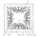
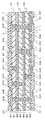
図1乃至図5は、本発明による実施例1の配線基板の概略構成を示す模式図であり、図1は本実施例1の配線基板の特徴を説明するための断面図、図2は本実施例1の配線基板を第1導体層側から見たときの平面図、図3は図2に示した配線基板の領域L1の拡大平面図、図4は図2に示した配線基板の領域L1の第2導体層を示す平面図、図5は図2に示した配線基板の領域L1の第3導体層を示す平面図である。また、図1は、図3のA−A’線での断面を示している。
【0043】
図1、図2、図3、図4、及び図5の各図において、M1は第1導体層、M2は第2導体層、M3は第3導体層、B1は第1絶縁層、B2は第2絶縁層、101は第1絶縁基板、102は第2絶縁基板、201Aはグラウンド用配線、201Bは電源用配線、201Cは信号用配線、202Aはグラウンドパターン、203Aはグラウンド用端子、203Bは電源用端子、203Cは信号用端子、302,303は電解銅めっき膜、302A,303A,303B,303Cはビア、4は埋め込み絶縁体、5ははんだ保護膜(ソルダレジスト)、6は端子めっきである。
【0044】
本実施例1の配線基板は、図1に示すように、第1絶縁体101からなる第1絶縁層B1の表面、言い換えると、半導体チップが搭載される面に第1導体層M1が設けられ、前記第1絶縁層B1の前記第1導体層M1が設けられた面と対向する面に第2導体層M2が設けられ、前記第1絶縁層M1に設けられた前記第2導体層M2の表面上に、第2絶縁体102からなる第2絶縁層B2を介在させて第3導体層M3が設けられた配線基板である。
【0045】
また、本実施例1の配線基板は、BGA(Ball Grid Array)やCSP(Chip Size Package)などの半導体装置に用いられるインターポーザであり、前記第1導体層M1には、図1、図2、及び図3に示すように、搭載される前記半導体チップの外部端子(ボンディングパッド)と接続される導体配線が設けられている。このとき、前記導体配線は、前記半導体チップにグラウンド電位の電源を供給する導体配線201A(以下、グラウンド用配線と称する)、前記半導体チップに、前記グラウンド電位と異なる電位の動作電源を供給する導体配線201B(以下、電源用配線と称する)、及び電気的信号を伝達する導体配線201C(以下、信号用配線と称する)がある。
【0046】
また、前記第2導体層M2には、図1に示したように、前記グラウンド用配線201Aと接続される導体パターン202A(以下、グラウンドパターンと称する)が設けられている。このとき、前記第1絶縁基板1の、前記グラウンドパターン202Aと前記グラウンド用配線201Aを接続する位置には、前記第1絶縁基板101を貫通する第1ビア穴VH1が設けられており、前記グラウンドパターン202Aの表面及び前記第1ビア穴VH1の内壁には、電解銅めっき膜302が設けられている。すなわち、前記グラウンドパターン202Aと前記グラウンド用配線201Aは、前記第1ビア穴VH1の内壁に設けられた電解銅めっき膜(ビア)302Aにより接続されている。
【0047】
また、前記第3導体層M3には、マザーボード等の実装基板の端子(配線)と接続される接続端子が設けられている。このとき、前記接続端子は、図1に示したように、前記グラウンドパターン202Aと接続される接続端子203A(以下、グラウンド用端子と称する)、前記電源用配線201Bと接続される接続端子203B(以下、電源用端子と称する)、及び前記信号用配線201Cと接続される接続端子203C(以下、信号用端子と称する)がある。
【0048】
またこのとき、前記グラウンド用端子203Aと前記グラウンドパターン202Aを接続する位置には、前記第2絶縁基板102を貫通する第2ビア穴VH2が設けられており、前記グラウンド用端子203Aの表面及び前記第2ビア穴VH2の内壁には、電解銅めっき膜303が設けられている。すなわち、前記グラウンド用端子203Aと前記グラウンドパターン202Aは、前記第2ビア穴VH2の内壁に設けられたビア303Aにより接続されている。
【0049】
また、前記電源用端子203Bと前記電源用配線201Bを接続する位置、及び前記信号用端子203Cと前記信号用配線201Cを接続する位置にはそれぞれ、前記第2絶縁基板102及び前記第1絶縁基板101を貫通する第3ビア穴VH3が設けられており、前記電源用端子203B及び前記信号用端子203Cの表面、ならびに前記第3ビア穴VH3の内壁にも前記電解銅めっき膜303が設けられている。すなわち、前記電源用端子203Bと前記電源用配線201Bは、前記第3ビア穴VH3の内壁に設けられたビア303Bにより直接接続されており、前記信号用端子203Cと前記信号用配線201Cは、前記第3ビア穴VH3の内壁に設けられたビア303Cにより直接接続されている。
【0050】
また、前記第2導体層M2に設けられた前記グラウンドパターン202Aは、図4に示すように、前記電源用配線201Bと前記電源用端子203Bを接続するビア303B、及び前記信号用配線201Cと前記信号用端子203Cを接続するビア303Cが通る周辺の領域を除く全面に広がっており、前記信号用配線201A、前記第1絶縁基板101、及び前記グラウンドパターン202Aによるマイクロストリップが構成されている。このとき、前記電源用端子203Bと前記電源用配線201Bを接続するビア303B、及び前記信号用端子203Cと前記信号用配線201Cを接続するビア303Cのそれぞれと、前記グラウンドパターン202Aの間は、図1及び図4に示したように、絶縁体4が埋め込まれ分離されている。また、前記グラウンドパターン202Aと前記グラウンド用配線201Aを接続するビア302Aの内部も、同様の絶縁体4が埋め込まれている。
【0051】
また、前記第3導体層M3に設けられた前記電源用端子203Bは、図5に示すように、前記グラウンド用端子203A、前記信号用端子203Cの周辺を除く全面に広がっている。
【0052】
また、前記第1導体層M1の表面(露出面)は、図1に示したように、前記各導体配線の、前記半導体チップの外部端子と接続される領域が開口するようにはんだ保護膜(ソルダレジスト)5が設けられており、前記各導体配線の露出面上には、例えば、金めっきなどの端子めっき6が設けられている。また、同様に、前記第3導体層M3の表面は、図1及び図5に示したように、マザーボード等の実装基板や他の外部装置の接続端子(配線)と接続される領域L3が開口するように、前記はんだ保護膜5が設けられており、前記各接続端子の露出面上に、前記端子めっき6が設けられている。
【0053】
また、本実施例1の配線基板は、BGA(Ball Grid Array)、CSP(Chip Size Package)などの半導体装置(パッケージ)において、前記半導体チップの外部端子と前記実装基板の接続端子(配線)の整合、あるいはグリッド変換を行うための配線基板(インターポーザ)であり、図5に示したような、前記電源層の前記端子めっき6が設けられた領域L3には、Sn-Pb系はんだ等のボール状端子が設けられる。
【0054】
また、本実施例1の配線基板では、前記グラウンド用端子203A及び前記電源用端子203Bを、前記信号用端子203Cの内側に設けて配線長を短くし、電圧降下などによる動作不良が起こりにくいようにしている。
【0055】
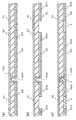
図6乃至図10は、本実施例1の配線基板の製造方法を説明するための模式断面図であり、図6(a)、図6(b)、図6(c)、図7(a)、図7(b)、図7(c)、図8(a)、図8(b)、図9(a)、図9(b)、図10(a)、図10(b)はそれぞれ、図3の断面図で見たときの各製造工程の断面図を示している。
【0056】
以下、図6乃至図10に沿って、本実施例1の配線基板の製造方法について説明する。
【0057】
まず、図6(a)に示すように、第1絶縁体101の第1主面に第1導体膜201’を形成し、前記第1絶縁体101の第2主面に第2導体膜202’を形成した積層板(両面銅張積層板)を準備する。このとき、前記第1絶縁体101は、マイクロストリップの効果を十分に得られるよう、誘電率が低く、且つ薄い材料であることが好ましく、例えば、厚さが25μm程度のポリイミドテープを用いる。また、前記第1導体膜201’及び前記第2導体膜202’は、例えば、前記第1絶縁体101の表面に、電解銅箔あるいは圧延銅箔などの銅箔を接着する方法や、前記第1絶縁層の表面に、スパッタリング等で薄膜を形成する方法などがある。またこのとき、前記第1導体膜201’及び前記第2導体膜202’は、例えば、厚さが12μm程度になるように形成する。
【0058】
次に、図6(b)に示すように、前記第2導体膜202’の所定位置を開口し、図6(c)に示すように、前記第1絶縁体101に第1ビア穴VH1を形成する。このとき、前記第1ビア穴VH1を形成する位置は、図1に示した、前記グラウンド用配線201Aと前記グラウンドパターン202Aを接続する位置であり、例えば、炭酸ガスレーザやエキシマレーザ等を用いたレーザ加工、あるいはエッチング処理により形成する。
【0059】
次に、図7(a)に示すように、前記第2導体膜202’の表面及び前記第1ビア穴VH1の内部に、例えば、厚さが約10μmの第3導体膜302を形成する。このとき、前記第3導体膜302は、例えば、電解銅めっきにより形成される。
【0060】
次に、図7(b)に示すように、前記第3導体膜(電解銅めっき膜)302及び前記第2導体膜202’をエッチング処理して前記グラウンドパターン202Aを形成した後、図7(c)に示すように、前記グラウンドパターン202の開口部及びビア内に絶縁体4を埋め込み、表面を平坦化する。このとき、前記グラウンドパターン202Aは、図4に示したように、前記電源用配線201Bと前記電源用端子203Bを接続するビア303B、及び前記信号用配線201Cと前記信号用端子203Cを接続するビア303Cを形成する領域の周辺が開口するようにエッチングする。
【0061】
次に、図8(a)に示すように、前記グラウンドパターン202Aの表面上に、第2絶縁体102を介在させて第4導体膜203’を形成する。このとき、例えば、第4導体膜203’として、電解銅箔あるいは圧延銅箔などの厚さが約12μmの銅箔を用い、前記第4導体膜(銅箔)203’の表面に、前記第2絶縁体102として、例えば、ポリイミドなどの未硬化の熱硬化性樹脂を塗布して硬化反応を中間段階まで進めたものを用意して接着する。
【0062】
次に、図8(b)に示すように、前記第4導体膜203’の所定位置を開口し、図9(a)に示すように、前記第2絶縁体102を貫通して前記グラウンドパターン202Aに達する第2ビア穴VH2と、前記第2絶縁体102、前記埋め込み絶縁体4、及び前記第1絶縁体101を貫通して前記第1導体膜201’に達する第3ビア穴VH3を形成する。このとき、前記第2ビア穴VH2と前記第3ビア穴VH3を形成する方法としては、例えば、図8(b)に示したように、所定位置を開口した前記第4導体膜203’をマスクとし、炭酸ガスレーザを用いて開口する方法が好ましい。前記炭酸ガスレーザによるエッチングは、絶縁体を選択的にエッチングし金属膜などはエッチングされないため、前記第1絶縁体101及び前記第2絶縁体、ならびに前記埋め込み絶縁体4を選択的にエッチングすることができる。そのため、深い方の前記第3ビア穴VH3の深さを基準にしてエッチングすると、前記第2ビア穴VH2は前記グラウンドパターン202A(第3導体膜302)に達したところでエッチングが終了し、前記第2ビア穴VH2及び前記第3ビア穴VH3の、深さの異なるビア穴を一度に形成することができる。
【0063】
次に、図9(b)に示すように、前記第4導体膜203’の表面、前記第2ビア穴VH2、及び前記第3ビア穴VH3の内壁に、厚さが約10μm程度の第5導体膜303を形成する。このとき、前記第5導体膜303は、例えば、電解銅めっきにより形成する。
【0064】
次に、図10に示すように、前記第1導体膜201’をエッチング処理して、前記グラウンド用配線201A、前記電源用配線201B、及び前記電源用配線201Cを形成し、前記第4導体203’及びその表面の第5導体膜(電解銅めっき膜)303をエッチング処理して、前記グラウンド用端子203A、電源用端子203B、及び信号用端子203Cを形成する。
【0065】
このとき、前記電源用端子203Bは、図5に示したように、前記グラウンド用端子203Aおよび信号用端子203Cの周辺を除く領域の全面に広がっている。
【0066】
その後、図3に示したように、前記第1導体層M1の各導体配線上、及び前記第3導体層M3の各接続端子の所定領域L3が開口するように、はんだ保護膜5を形成し、前記各導体配線及び前記各接続端子露出面に、例えば、金めっきなどの端子めっき6を形成すると、本実施例1の配線基板となる。
【0067】
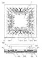
図11は、本実施例1の配線基板の作用効果を説明するための模式平面図である。
【0068】
本実施例1の配線基板は、図1に示したように、前記第1導体層M1、前記第2導体層M2、及び前記第3導体層M3の3層の導体層を有する配線基板であり、前記第2導体層M2は、図4に示したように、前記電源用配線201Bと前記電源用端子203Bを接続するビア303B、及び前記信号用配線201Cと前記信号用端子203Cを接続するビア303Cの周辺のみが開口した平板状の導体パターン(グラウンドパターン)202Aからなる。
【0069】
前記グラウンドパターン202Aに形成された開口部は、前記グラウンドパターン202Aと前記各ビア303B,303Cが接触しない程度の大きさであればよいため、図11に示したように、前記第1導体層M1に形成された前記導体配線、特に、前記信号用配線201Cが、前記グラウンドパターン202Aの開口部上、すなわち、埋め込み用の絶縁体4上を通らないように形成することができる。そのため、前記図23に示した、従来の導体層が2層の配線基板のように、前記信号用配線201Cが前記電源用端子202B及び前記信号用端子202C上を通ることを防げ、前記信号用配線201Cの全区間において、前記信号用配線201C、前記第1絶縁体101、及び前記グラウンドパターン202Aからなるマイクロストリップの効果を十分に得られ、特性インピーダンスの制御が容易になる。また、マイクロストリップの効果を十分に得られ、特性インピーダンスの制御が容易になることにより、前記信号用配線201Cを流れる電気的信号にノイズが発生しにくくなるため、高周波特性の劣化を低減することができる。
【0070】
図12乃至図13は、本実施例1の配線基板を用いた半導体装置の概略構成を示す模式図であり、図12(a)は半導体装置の平面図、図12(b)は図11(a)の側面図、図13は図12(a)の半導体装置の内部構成を示す断面図である。
【0071】
本実施例1の配線基板は、BGA、CSP等の半導体装置のインターポーザとして用いられ、図12(a)、図12(b)、及び図13に示すように、前記配線基板の第1導体層M1側、すなわち、前記グラウンド用配線201A、前記電源用配線201B、及び前記信号用配線201Cが設けられた面に、半導体チップ7がフリップチップ接続される。このときの接続には、前記半導体チップ7の外部端子(ボンディングパッド)701に、例えば、高融点はんだのバンプ8を形成しておき、前記配線基板の前記各導体配線上に設けられた端子めっき6の表面に、低融点はんだ(図示しない)を塗布しておいて熱圧着する方法がとられる。
【0072】
また、前記配線基板と半導体チップ7の間には、例えば、未硬化の熱硬化性樹脂のような封止絶縁体9を流し込んだ後、硬化させてアンダーフィル封止されている。また、前記配線基板は、非常に薄く強度が弱いため、前記半導体チップ7が搭載された領域の外側が変形しやすいので、図12(b)に示したように、金属製のカバープレート10で前記半導体チップ7を覆うとともに、前記配線基板の補強をする。
【0073】
また、前記配線基板の第3導体層M3に設けられた前記グラウンド用端子201A、前記電源用端子201B、及び前記信号用端子201Cのそれぞれには、図12(b)に示したように、例えば、Sn-Pb系はんだなどのボール状端子11が接続される。
【0074】
以上説明したように、本実施例1の配線基板によれば、前記第1導体層M1、前記第2導体層M2、及び前記第3導体層M3の3層の導体層を設け、前記第1導体層M1に、半導体チップの外部端子と接続される導体配線を設け、前記第2導体層M2に前記第1導体層の導体配線のうち、グラウンド電位の電源を供給する導体配線(グラウンド用配線)201Aと接続される導体パターン(グラウンドパターン)202Aを設け、前記第3導体層に実装基板の端子(配線)と接続される接続端子を設けることにより、前記第2導体層M2に設けられた前記グラウンドパターン202Aの面積を広くすることができる。そのため、前記第1導体層M1の電気的信号を伝達する導体配線(信号用配線)201Cが、全区間で前記グラウンドパターン202A上を通るようにすることができ、前記信号用配線201C、前記第1絶縁体101、及び前記グラウンドパターン202Aからなるマイクロストリップの効果を十分に得られ、特性インピーダンスの制御が容易になる。また、特性インピーダンスの制御が容易になるため、前記信号用配線201Cを流れる電気的信号にノイズが発生しにくくなり、高周波特性が劣化するのを防げる。
【0075】
またこのとき、前記第1導体層M1に設けられた前記電源用配線201Bと前記第3導体層M3に設けられた前記電源用端子201Bを接続するビア303B、及び前記第1導体層M1に設けられた前記信号用配線201Cと前記第3導体層M3に設けられた前記信号用端子201Cを接続するビア303Cを、前記第1絶縁体101、前記埋め込み絶縁体4、及び前記第2絶縁体102を貫通する前記第3ビア穴VH3の内壁に設けて直接接続することにより、例えば、スタックビアで接続する場合に比べて製造工程が少なくなるとともに、2段以上のビアを重ねたときの位置ずれなどによる接続信頼性の低下がなくなり、接続信頼性の高い配線基板を安価で得ることができる。
【0076】
また、前記第1導体層M1に設けられた前記電源用配線201Bと前記第3導体層M3に設けられた前記電源用端子201Bを接続するビア303B、及び前記第1導体層M1に設けられた前記信号用配線201Cと前記第3導体層M3に設けられた前記信号用端子201Cを接続するビア303Cを、前記第1絶縁体101、前記埋め込み絶縁体4、及び前記第2絶縁体102を貫通する前記第3ビア穴VH3の内壁に設けて直接接続することにより、スタックビアで接続する場合に比べ、前記グラウンドパターン202Aに形成する開口部の面積を小さくすることができ、前記信号用配線201Cが前記グラウンドパターン202Aの開口部上を通る可能性がさらに低減し、電気的信号の高周波特性が劣化することを防げる。
【0077】
また、前記第1導体層M1に設けられた前記電源用配線201Bと前記第3導体層M3に設けられた前記電源用端子203Bを接続するビア303B、及び前記第1導体層M1に設けられた前記信号用配線201Cと前記第3導体層M3に設けられた前記信号用端子203Cを接続するビア303Cを、前記第1絶縁体101、前記埋め込み絶縁体4、及び前記第2絶縁体102を貫通する前記第3ビア穴VH3の内壁に設けて直接接続し、前記グラウンドパターン202Aの開口部の面積を小さくすることにより、前記各ビア303B,303Cの間隔を狭めることができ、配線基板の小型化、前記導体配線の微細化が容易になる。
【0078】
また、前記第3導体層M3に設けられた各接続端子のうち、前記電源用端子203Bを、前記グラウンド用端子203A及び前記信号用端子203Cの周辺を除く領域の全面に広げることにより、前記信号用配線201Cに高周波信号が流れたときのインダクタとしての作用を低減させることができる。
【0079】
図14は、前記実施例1の配線基板の変形例を説明するための模式断面図であり、図1の断面と同じ断面を示している。
【0080】
前記実施例1の配線基板では、図10に示したように、前記第1導体層M1の前記グラウンド用配線201A、前記電源用配線201B、及び前記信号用配線201Cを形成し、前記第3導体層M3の前記グラウンド用端子203A、前記電源用端子203B、及び前記信号用端子203Cを形成した後、前記第1導体層M1の表面及び前記第3導体層M3の表面にはんだ保護膜5を形成しているが、これに限らず、例えば、前記第3導体層M3の表面に前記はんだ保護膜5を形成する前に、前記第3導体層M3の各接続端子を分離する部分及び前記各ビアの内部に絶縁体4を埋め込んでもよい。
【0081】
例えば、前記実施例1の配線基板のように、前記第3導体層M3の各接続端子を形成した後、直接前記はんだ保護膜5を形成した場合、前記電源用配線201Bと前記電源用端子203Bを接続するビア303Bや、前記信号用配線201Cと前記信号用端子203Cを接続するビア303Cのように深いビアの内部に、気泡ができてしまう可能性がある。このとき、例えば、前記半導体装置を動作させ、半導体チップや配線基板が高熱になり、例えば、図12(b)に示したような前記カバープレート10からの放熱が間に合わないと、前記気泡が膨張して、前記各ビアにクラックが生じたり、断線したりして電気的特性が悪くなる可能性がある。そのため、図14に示したように、絶縁体4を埋め込むことにより、前記各ビア内に気泡ができるのを防ぎ、電気的特性が悪くなることを防げる。
【0082】
(実施例2)
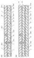
図15は、本発明による実施例2の配線基板の概略構成を示す模式断面図である。
【0083】
図15において、M1は第1導体層、M2は第2導体層、M3は第3導体層、M4は第4導体層、B1は第1絶縁層、B2は第2絶縁層、B3は第3絶縁層、101は第1絶縁基板、102は第2絶縁基板、103は第3絶縁基板、201Aはグラウンド用配線、201Cは信号用配線、201Dは第1電源用配線、201Eは第2電源用配線、202Aはグラウンドパターン、203Dは第1電源パターン、204Aはグラウンド用端子、204Cは信号用端子、204Dは第1電源用端子、204Eは第2電源用端子、302,303,304は電解銅めっき膜、302A,303D,304A,304C,304D,304Eはビア、4は埋め込み絶縁体、5ははんだ保護膜(ソルダレジスト)、6は端子めっきである。
【0084】
本実施例2の配線基板は、図15に示すように、第1絶縁体101からなる第1絶縁層B1の表面、言い換えると、半導体チップが搭載される面に第1導体層M1が設けられ、前記第1絶縁層B1の前記第1導体層M1が設けられた面と対向する面に第2導体層M2が設けられ、前記第1絶縁層M1に設けられた前記第2導体層M2の表面上に、第2絶縁体102からなる第2絶縁層B2を介在させて第3導体層M3が設けられ、前記第3導体層M3の表面上に、第3絶縁体103からなる第4導体層M4が設けられた配線基板である。
【0085】
また、本実施例2の配線基板も、前記実施例1の配線基板と同様で、BGAやCSPなどの半導体装置に用いられるインターポーザであり、前記第1導体層M1には、図15に示したように、搭載される前記半導体チップの外部端子(ボンディングパッド)と接続される導体配線が設けられている。このとき、前記導体配線は、前記半導体チップにグラウンド電位の電源を供給する導体配線201A(以下、グラウンド用配線と称する)、前記半導体チップに前記グラウンド電位と異なる第1電位の動作電源を供給する導体配線201D(以下、第1電源用配線と称する)、前記半導体チップに前記グラウンド電位及び第1電位と異なる第2電位の動作電源を供給する導体配線201E(以下、第2電源用配線と称する)、及び電気的信号を伝達する導体配線201C(以下、信号用配線と称する)がある。またこのとき、前記第1電源用配線201Dで供給する動作電源の電位は、例えば、1.8V(ボルト)であり、前記第2電源用配線201Eで供給する動作電源の電位は、例えば、3.3V(ボルト)とする。
【0086】
また、前記第2導体層M2には、図15に示したように、前記グラウンド用配線201Aと接続される導体パターン202A(以下、グラウンドパターンと称する)が設けられている。また、前記第1絶縁基板1の、前記グラウンドパターン202Aと前記グラウンド用配線201Aを接続する位置には、前記第1絶縁基板101を貫通する第1ビア穴VH1が設けられており、前記グラウンドパターン202Aの表面及び前記第1ビア穴VH1の内壁には、電解銅めっき膜302が設けられている。すなわち、前記グラウンドパターン202Aと前記グラウンド用配線201Aは、前記第1ビア穴VH1の内壁に設けられた電解銅めっき膜(ビア)302Aにより接続されている。
【0087】
また、前記第3導体層M3には、図15に示したように、前記第1電源用配線201Dと接続される導体パターン203D(以下、第1電源パターンと称する)が設けられている。このとき、前記第1電源パターン203Dと前記第1電源用配線201Dを接続する位置には、前記第1絶縁基板101及び前記第2絶縁基板102を貫通する第2ビア穴VH2が設けられており、前記第1電源パターン203Dの表面及び前記第2ビア穴VH2の内壁には、電解銅めっき膜303が設けられている。すなわち、前記第1電源パターン203Dと前記第1電源用配線201Dは、前記第2ビア穴VH2の内壁に設けられた電解銅めっき膜(ビア)303Dにより接続されている。
【0088】
また、前記第4導体層M4には、マザーボード等の実装基板の端子(配線)と接続される接続端子が設けられている。このとき、前記接続端子は、図15に示したように、前記グラウンドパターン202Aと接続される接続端子204A(以下、グラウンド用端子と称する)、前記第1電源用配線201Dと接続される接続端子204D(以下、第1電源用端子と称する)、前記第2電源用配線201Eと接続される接続端子204E(以下、第2電源用端子と称する)、及び前記信号用配線201Cと接続される接続端子204C(以下、信号用端子と称する)がある。
【0089】
このとき、前記グラウンド用端子204Aと前記グラウンドパターン202Aを接続する位置には、前記第2絶縁基板102及び前記第3絶縁基板103を貫通する第3ビア穴VH3が設けられており、前記グラウンド用端子204Aの表面及び前記第3ビア穴VH3の内壁には、電解銅めっき膜304が設けられている。すなわち、前記グラウンド用端子204Aと前記グラウンドパターン202Aは、前記第3ビア穴VH3の内壁に設けられたビア304Aにより接続されている。
【0090】
また、前記第1電源用端子204Dと前記第1電源パターン203Dを接続する位置には、前記第3絶縁基板103を貫通する第4ビア穴VH4が設けられており、前記第1電源用端子204Dの表面及び前記第4ビア穴VH4の内壁には、電解銅めっき膜304が設けられている。すなわち、前記第1電源用端子204Dと前記第1電源パターン203Dは、前記第4ビア穴VH4の内壁に設けられたビア304Dにより接続されている。
【0091】
また、前記第2電源用端子204Eと前記第2電源信号201Eを接続する位置、及び前記信号用端子204Cと前記信号用配線201Cを接続する位置にはそれぞれ、前記第3絶縁基板103、前記第2絶縁基板102、及び前記第1絶縁基板101を貫通する第5ビア穴VH5が設けられており、前記第2電源用端子204E及び前記信号用端子204Cの表面、ならびに前記第5ビア穴VH5の内壁にも前記電解銅めっき膜304が設けられている。すなわち、前記第2電源用端子204Eと前記第2電源用配線201Eは、前記第5ビア穴VH5の内壁に設けられたビア304Eにより接続されており、前記信号用端子204Cと前記信号用配線201Cは、前記第5ビア穴VH5の内壁に設けられたビア304Cにより接続されている。
【0092】
また、前記第2導体層M2に設けられた前記グラウンドパターン202Aは、前記実施例1の配線基板のグラウンドパターンと同様であり、前記第1電源用配線201Dと前記第1電源パターン203Dを接続するビア303D、前記第2電源用配線201Eと前記第2電源用端子204Dを接続するビア304E、及び前記信号用配線201Cと前記信号用端子204Cを接続するビア304Cが通る周辺の領域を除く全面に広がっており、前記信号用配線201C、前記第1絶縁基板101、及び前記グラウンドパターン202Aからなるマイクロストリップが構成されている。
【0093】
またこのとき、前記第1電源パターン203Dと前記第1電源用配線201Dを接続するビア303D、前記第2電源用端子204Eと前記第2電源用配線201Eを接続するビア304E、及び前記信号用端子204Cと前記信号用配線201Cを接続するビア304Cのそれぞれと、前記グラウンドパターン202Aの間は、図15に示したように、絶縁体4が埋め込まれ分離されている。また、前記グラウンドパターン202Aと前記グラウンド用配線201Aを接続するビア302Aの内部も、同様の絶縁体4が埋め込まれている。
【0094】
また、前記第4導体層M4に設けられた前記第2電源用端子204Eは、前記実施例1の配線基板の電源用端子203Bと同様に、前記グラウンド用端子204A、前記第1電源用端子204D、及び前記信号用端子204Cの周辺を除く全面に広がっている。
【0095】
また、前記第1導体層M1の表面(露出面)は、図15に示したように、前記各導体配線の、前記半導体チップの外部端子と接続される領域の外部が、はんだ保護膜(ソルダレジスト)5により保護されており、前記各導体配線の露出面上には、例えば、金めっきなどの端子めっき6が設けられている。また、同様に、前記第4導体層M4の表面は、マザーボード等の実装基板や他の外部装置の接続端子(配線)と接続される領域の外部が、前記はんだ保護膜5により保護されており、前記各接続端子の露出面上に、前記端子めっき6が設けられている。
【0096】
また、本実施例2の配線基板は、BGA、CSPなどの半導体装置(パッケージ)において、前記半導体チップの外部端子と前記実装基板の接続端子(配線)の整合、あるいはグリッド変換を行うための配線基板(インターポーザ)であるため、図15に示したような、前記第4導体層M4の各接続端子の、前記端子めっき6が設けられた部分には、Sn-Pb系はんだ等のボール端子が設けられる。
【0097】
また、本実施例2の配線基板でも、前記実施例1の配線基板と同様で、電圧降下などによる特性の劣化を防ぐために、前記グラウンド用端子204A、前記第1電源用端子204D及び前記第2電源用端子204Eを、前記信号用端子204Cの内側に設け、配線長が短くなるようにしている。
【0098】
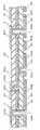
図16乃至図18は、本実施例2の配線基板の製造方法を説明するための模式断面図であり、図16(a)、図16(b)、図17(a)、図17(b)、図18(a)、図18(b)はそれぞれ、図15の断面と同じ断面で見たときの各製造工程の断面図を示している。
【0099】
以下、図16乃至図18に沿って、本実施例2の配線基板の製造方法について説明するが、前記実施例の配線基板の製造方法と同様の工程については、その詳細な説明を省略する。
【0100】
まず、前記実施例1で説明した手順に沿って、図16(a)に示すような、第1絶縁基板101の表面に第1導体膜201’が形成され、前記第1絶縁基板101の前記第1導体膜201’が形成された面と対向する面に、前記グラウンドパターン202Aが形成された積層体の、前記グラウンドパターン202A上に、第2絶縁体102を介在させて第4導体膜203’を形成する。
【0101】
次に、前記第4導体膜203’側から、前記第2絶縁体102、前記埋め込み絶縁体4、及び前記第1絶縁体101を貫通して前記第1導体膜201’に達する第2ビア穴VH2を開口した後、図16(b)に示すように、前記第4導体膜203’の表面、及び前記第2ビア穴VH2の内壁に第5導体膜(電解銅めっき膜)303を形成する。
【0102】
次に、前記第4導体膜203’及びその表面の電解銅めっき膜303をエッチング処理して、前記第1電源パターン203Dを形成した後、図17(a)に示すように、前記第1電源パターン203Dの開口部内、及び前記ビア303D内に絶縁体4を埋め込み、表面を平坦化する。このとき、前記第1電源パターン202Dは、前記グラウンド用端子204Aと前記グラウンドパターン202Aを接続するビア304A、前記第2電源用端子204Eと前記第2電源用端子201Eを接続するビア304E、及び前記信号用端子204Cと前記信号用配線201Aを接続するビア304Cを形成する領域の周辺のみが開口するようにエッチングされる。
【0103】
次に、図17(b)に示すように、前記第1電源パターン203Dの表面上に、第3絶縁体103を介在させて第6導体膜204’を形成する。
【0104】
次に、前記第6導体膜204’側から、前記第3絶縁基板103、前記埋め込み絶縁体4、及び前記第2絶縁体102を貫通して前記グラウンドパターン202Aに達する第3ビア穴VH3、前記第3絶縁基板103を貫通して前記第1電源パターン203Dに達する第4ビア穴VH4、及び前記第3絶縁基板103、前記埋め込み絶縁体4、前記第2絶縁基板102、前記埋め込み絶縁体4、前記第1絶縁基板101を貫通して前記第1導体膜201’に達する第5ビア穴VH5を形成した後、図18(a)に示すように、前記第6導体膜204’の表面、及び前記第3ビア穴VH3、前記第4ビア穴VH4、前記第5ビア穴VH5の内壁に第7導体膜(電解銅めっき膜)304を形成する。
【0105】
このとき、前記第3ビア穴VH3、前記第4ビア穴VH4、及び前記第5ビア穴VH5を形成する方法としては、前記実施例1の配線基板の製造方法における前記第2ビア穴VH2及び前記第3ビア穴VH3の形成方法と同じく、所定位置を開口した前記第6導体膜204’をマスクとし、炭酸ガスレーザを用いて開口する方法が好ましい。前記炭酸ガスレーザによるエッチングは、絶縁体を選択的にエッチングし金属膜などはエッチングされないため、前記第1絶縁体101、前記第2絶縁体102、及び前記第3絶縁体103、ならびに前記埋め込み絶縁体4を選択的にエッチングすることができる。すなわち、最も深い前記第5ビア穴VH5の深さを基準にしてエッチングすると、まず、前記第4ビア穴VH4が前記第1電源パターン203D(第5導体膜303)に達してエッチングの進行がとまり、次に、前記第3ビア穴VH3が前記グラウンドパターン202A(第3導体膜302)に達してエッチングの進行がとまる。そして最後に、前記第5ビア穴VH5が前記第1導体膜201’に達したところで全体のエッチング処理が終了する。そのため、前記第3ビア穴VH3、前記第4ビア穴VH4、及び前記第5ビア穴VH5の、深さの異なるビア穴を一度に形成することができる。
【0106】
次に、図18(b)に示したように、前記第1導体膜201’をエッチング処理して、前記グラウンド用配線201A、前記第1電源用配線201D、前記第2電源用配線201E、及び前記信号用配線201Cを形成し、前記第6導体膜204’及びその表面の前記第7導体膜304をエッチング処理して、前記グラウンド用端子204A、前記第1電源用端子204D、前記第2電源用端子204E、及び前記信号用端子204Cを形成する。
【0107】
その後、図15に示したように、前記第1導体層M1の各導体配線上、及び前記第4導体層M4の各接続端子の所定領域が開口するように、はんだ保護膜5を形成し、前記各導体配線及び前記各接続端子露出面に、例えば、金めっきなどの端子めっき6を形成すると、本実施例2の配線基板となる。
【0108】
本実施例2の配線基板においても、前記実施例1の配線基板と同様で、前記第1導体層M1の導体配線、特に、前記信号用配線201Cは全区間にわたり、図11に示したように、前記第2導体層M2に設けられた前記グラウンドパターン上を通るように形成することができ、前記信号用配線201C、前記第1絶縁基板101、及び前記グラウンドパターン202Aからなるマイクロストリップの効果を十分に得ることができる。
【0109】
以上説明したように、本実施例2の配線基板によれば、前記第1導体層M1、前記第2導体層M2、前記第3導体層M3、及び前記第4導体層M4の4層の導体層を設け、前記第1導体層M1に、半導体チップの外部端子と接続される導体配線を設け、前記第2導体層M2に前記第1導体層の導体配線のうち、グラウンド電位の電源を供給する導体配線(グラウンド用配線)201Aと接続される導体パターン(グラウンドパターン)202Aを設け、前記第4導体層に実装基板の端子(配線)と接続される接続端子を設けることにより、前記第2導体層M2に設けられた前記グラウンドパターン202Aの面積を広くすることができる。そのため、前記第1導体層M1の電気的信号を伝達する導体配線(信号用配線)201Cが、全区間で前記グラウンドパターン202A上を通るようにすることができ、前記信号用配線201C、前記第1絶縁体101、及び前記グラウンドパターン202Aからなるマイクロストリップの効果を十分に得られ、特性インピーダンスの制御が容易になる。また、特性インピーダンスの制御が容易になるため、前記信号用配線201Cを流れる電気的信号にノイズが発生しにくくなり、高周波特性が劣化するのを防げる。
【0110】
また、前記第3導体層M3に前記第1電源パターン203Dを設け、前記第4導体層M4に、他の端子の周辺を除く領域の全面に広がる第2電源用端子204Eを設けることにより、電位の異なる2種類の動作電源を供給する場合でも、書く電位の電源間の干渉や高周波信号による電気的特性の劣化を低減することができる。
【0111】
またこのとき、前記第1導体層M1に設けられた前記第1電源用配線201Dと前記第3導体層M3に設けられた前記第1電源パターン203Dを接続するビア303Dを前記第1絶縁基板101、前記埋め込み絶縁体4、及び前記第2絶縁体102を貫通する第2ビア穴VH2の内壁に設けて直接接続し、前記第1導体層M1に設けられた前記第2電源用配線201Eと前記第4導体層M4に設けられた前記第2電源用端子204Eを接続するビア304E、及び前記第1導体層M1に設けられた前記信号用配線201Cと前記第4導体層M4に設けられた前記信号用端子204Cを接続するビア304Cを、前記第1絶縁体101、前記埋め込み絶縁体4、及び前記第2絶縁体102を貫通する前記第5ビア穴VH5の内壁に設けて直接接続することにより、例えば、スタックビアで接続する場合に比べて製造工程が少なくなるとともに、2段以上のビアを重ねたときの位置ずれなどによる接続信頼性の低下がなくなり、接続信頼性の高い配線基板を得ることができる。
【0112】
また、前記第1導体層M1に設けられた前記第1電源用配線201Dと前記第3導体層M3に設けられた前記第1電源パターン203Dを接続するビア303Dを前記第1絶縁基板101、前記埋め込み絶縁体4、及び前記第2絶縁体102を貫通する第2ビア穴VH2の内壁に設けて直接接続し、前記第1導体層M1に設けられた前記第2電源用配線201Eと前記第4導体層M4に設けられた前記第2電源用端子204Eを接続するビア304E、及び前記第1導体層M1に設けられた前記信号用配線201Cと前記第4導体層M4に設けられた前記信号用端子204Cを接続するビア304Cを、前記第1絶縁体101、前記埋め込み絶縁体4、及び前記第2絶縁体102を貫通する前記第5ビア穴VH5の内壁に設けて直接接続することにより、前記グラウンドパターン202Aに形成する開口部の面積を小さくすることができ、前記信号用配線201Cが前記グラウンドパターン202Aの開口部上を通る可能性がさらに低減し、電気的信号の高周波特性が劣化することを防げる。
【0113】
またこのとき、前記グラウンドパターン202Aの開口部の面積を小さくすることにより、前記実施例1の配線基板と同様に、前記各ビアの間隔を狭めることができ、配線基板の小型化、前記導体配線の微細化が容易になる。
【0114】
以上、本発明を、前記実施例に基づき具体的に説明したが、本発明は、前記実施例に限定されるものではなく、その要旨を逸脱しない範囲において種々変更可能であることはもちろんである。
【0115】
【発明の効果】
本発明において開示される発明のうち、代表的なものによって得られる効果を簡単に説明すれば、以下のとおりである。
【0116】
(1)マイクロストリップ構造の配線基板において、特性インピーダンスの制御を容易にすることができる。
【0117】
(2)マイクロストリップ構造の配線基板において、電気的信号の高周波特性の劣化を防ぐことができる。
【0118】
(3)マイクロストリップ構造の配線基板において、微細化を容易にすることができる。
【図面の簡単な説明】
【図1】本発明による実施例1の配線基板の概略構成を示す模式図であり、配線基板の特徴を示す断面図である。
【図2】本実施例1の配線基板の概略構成を示す模式図であり、配線基板全体の平面図である。
【図3】本実施例1の配線基板の概略構成を示す模式図であり、図2に示した配線基板の領域L1の拡大平面図である。
【図4】本実施例1の配線基板の概略構成を示す模式図であり、図3に示した平面図の第2導体層の構成を示す平面図である。
【図5】本実施例1の配線基板の概略構成を示す模式図であり、図3に示した平面図の第3導体層の構成を示す平面図である。
【図6】本実施例1の配線基板の製造方法を説明するための模式図であり、図6(a)、図6(b)、図6(c)はそれぞれ、図1に示した断面と同じ断面で見たときの、各工程での断面図である。
【図7】本実施例1の配線基板の製造方法を説明するための模式図であり、図7(a)、図7(b)、図7(c)はそれぞれ、図1に示した断面と同じ断面で見たときの、各工程での断面図である。
【図8】本実施例1の配線基板の製造方法を説明するための模式図であり、図8(a)、図8(b)はそれぞれ、図1に示した断面と同じ断面で見たときの、各工程での断面図である。
【図9】本実施例1の配線基板の製造方法を説明するための模式図であり、図9(a)、図9(b)はそれぞれ、図1に示した断面と同じ断面で見たときの、各工程での断面図である。
【図10】本実施例1の配線基板の製造方法を説明するための模式図であり、図10(a)、図10(b)はそれぞれ、図1に示した断面と同じ断面で見たときの、各工程での断面図である。
【図11】本実施例1の配線基板の作用効果を説明するための模式平面図である。
【図12】本実施例1の配線基板を用いた半導体装置の概略構成を示す模式図であり、図12(a)は半導体装置全体の平面図、図12(b)は図12(a)に示した半導体装置の正面図である。
【図13】本実施例1の配線基板を用いた半導体装置の概略構成を示す模式図であり、図12(a)に示した半導体装置の内部構成を示す断面図である。
【図14】前記実施例1の配線基板の変形例を示す模式断面図である。
【図15】本発明による実施例2の配線基板の概略構成を示す模式断面図である。
【図16】本実施例2の配線基板の製造方法を説明するための模式図であり、図16(a)、図16(b)はそれぞれ、図15に示した断面と同じ断面で見たときの、各工程での断面図である。
【図17】本実施例2の配線基板の製造方法を説明するための模式図であり、図17(a)、図17(b)はそれぞれ、図15に示した断面と同じ断面で見たときの、各工程での断面図である。
【図18】本実施例2の配線基板の製造方法を説明するための模式図であり、図18(a)、図18(b)はそれぞれ、図15に示した断面と同じ断面で見たときの、各工程での断面図である。
【図19】従来の半導体装置の概略構成を示す模式図であり、図19(a)は半導体装置全体の平面図、図19(b)は図19(a)に示した半導体装置の正面図である。
【図20】従来の半導体装置に用いられる配線基板の概略構成を示す模式断面図である。
【図21】従来の半導体装置に用いられる配線基板の概略構成を示す模式平面図である。
【図22】従来の半導体装置に用いられる配線基板の概略構成を示す模式平面図である。
【符号の説明】
1 絶縁基板
101 第1絶縁基板
102 第2絶縁基板
103 第3絶縁基板
201A グラウンド用配線
201B 電源用配線
201C 信号用配線
201D 第1電源用配線
201E 第2電源用配線
202A,203A,204A グラウンドパターン(グラウンド用端子)
202B,203B,204B 電源用端子
202C,203C,204C 信号用端子
203D 第1電源パターン
204D 第1電源用端子
204E 第2電源用端子
201’ 第1導体膜
202’ 第2導体膜
203’ 第4導体膜
204’ 第6導体膜
302 第3導体膜(電解銅めっき膜)
303 第5導体膜(電解銅めっき膜)
304 第7導体膜(電解銅めっき膜)
302A,303A,303B,303C,303D,304A,304C,304D,304E ビア
4 埋め込み絶縁体
5 はんだ保護膜
6 端子めっき
7 半導体チップ
701 半導体チップの外部端子
8 バンプ
9 封止絶縁体
10 カバープレート
11 ボール状端子
M1 第1導体層
M2 第2導体層
M3 第3導体層
M4 第4導体層
B1 第1絶縁層
B2 第2絶縁層
B3 第3絶縁層[0001]
BACKGROUND OF THE INVENTION
The present invention relates to a wiring board and a manufacturing method thereof, and in particular, a signal wiring layer is provided on one main surface of an insulating layer, and a ground surface on the main surface of the insulating layer opposite to the main surface provided with the signal wiring layer is provided. The present invention relates to a technique that is effective when applied to a microstrip-structured wiring board provided with a layer or a power supply layer.
[0002]
[Prior art]
Conventionally, as shown in FIGS. 19A and 19B, a BGA (Ball Grid Array) type semiconductor device has a wiring board (on which a
[0003]
Further, in the case of the semiconductor device as shown in FIGS. 19A and 19B, the wiring substrate is formed on the
[0004]
The wiring board used in the BGA type semiconductor device may be, for example, an alignment between an external terminal (bonding pad) of the
[0005]
Further, the surface of the first conductor layer M1 is soldered so that portions of the
[0006]
Further, the second conductor layer M2 on the surface of the
[0007]
At this time, the
[0008]
Further, the surface of the second conductor layer M2 is solder-protected so that a region L3 connected to the ball-
[0009]
In addition, the BGA type semiconductor device as shown in FIGS. 19A and 19B has been increased in operation speed (high frequency) in recent years, and is on a wiring board used in the semiconductor device. As shown in FIGS. 20 and 22, the
[0010]
When the
[0011]
[Problems to be solved by the invention]
However, in the conventional technique, when the
[0012]
When the size of the wiring board is reduced, the conductor wiring provided on the wiring board is miniaturized, or when the number of the external connection terminals is increased due to higher functions of a semiconductor chip, the
[0013]
As described above, since the
[0014]
Further, if the
[0015]
An object of the present invention is to provide a technique capable of facilitating control of characteristic impedance in a microstrip structure wiring board.
[0016]
Another object of the present invention is to provide a technique capable of preventing deterioration of high frequency characteristics of an electrical signal in a microstrip structure wiring board.
[0017]
Another object of the present invention is to provide a technique capable of facilitating miniaturization in a wiring board having a microstrip structure.
[0018]
The above and other objects and novel features of the present invention will be apparent from the description of this specification and the accompanying drawings.
[0019]
[Means for Solving the Problems]
The outline of the invention disclosed in the present invention will be described as follows.
[0020]
(1) A first conductor layer is provided on a surface of the first insulating layer, a second conductor layer is provided on a surface of the first insulating layer opposite to a surface on which the first conductor layer is provided, and the first conductor layer is provided. A wiring board in which a third conductor layer is provided on the second conductor layer provided on the insulating layer with a second insulating layer interposed therebetween, and the first conductor layer has an external terminal ( Bonding pad)Multiple Conductor wiring is provided, and the second conductor layer includes the first conductor layer.of SaidMultiple Out of conductor wiringof ,Above Ground wiring for supplying ground potential power to semiconductor chipsIn Only the connected conductor pattern is provided, and the third conductor layer includes the first conductor layer.of SaidMultiple Out of conductor wiringof A power supply wiring for supplying an operating power supply with a potential other than the ground potential to the semiconductor chipIn ConnectedThe Power supply terminalWhen, SaidDifferent from ground wiring and power wiring Signal wiringClose to ContinuedThe Signal terminalWhen, The conductor pattern of the second conductor layerTo the ground wiring via ConnectedThe There is a ground terminal,The power supply wiring and the power supply terminal, and the signal wiring and the signal terminal are directly connected by vias penetrating the first insulating layer and the second insulating layer, respectively. Is spread over the entire surface excluding the periphery of the ground terminal and the signal terminal, The second conductor layerOf the above The conductor pattern includes the power supply wiring and the power supply terminal.When Connecting via, And the signal wiring and the signalTerminal and Spread over the entire area except the periphery of the viaAn annular region that separates a conductor pattern of the second conductor layer and a via that connects the power supply wiring and the power supply terminal between the first insulating layer and the second insulating layer; and An insulator is embedded in each of the vias connecting the signal wiring and the signal terminals and the conductor pattern annular regions of the second conductor layer. It is a wiring board.
[0021]
According to the means of (1), a conductor pattern connected to the ground wiring is provided on the second conductor layer, and the ground terminal, the power supply terminal, and the signal terminal are connected to the third conductor layer. By providing in, the area of the said conductor pattern provided in the said 2nd conductor layer can be enlarged. Therefore, the conductor wiring provided in the first conductor layer, in particular, the signal wiring can be prevented from passing over the region without the conductor pattern, and the signal wiring and the first insulating layer can be prevented. And the characteristic impedance can be easily controlled by the microstrip of the conductor pattern.
[0022]
Further, since the signal wiring can always pass on the conductor pattern, noise due to mutual impedance between the conductor wirings can be reduced, and deterioration of the high-frequency characteristics of the signal to be transmitted can be prevented.
[0023]
In addition, since the signal wiring increases in signal speed, that is, as the signal becomes higher in frequency, an action as an inductor occurs. Therefore, in the wiring board of the means of (1), the power supply terminal is connected. The action of the signal wiring as an inductor can be reduced by extending the entire area excluding the periphery of the ground terminal and the signal terminal.
[0024]
In the wiring board of the means (1), as a method of connecting the conductor wiring of the first conductor layer and the terminal of the third conductor layer by vias, the first insulating layer and the second insulating layer are A direct connection method using vias provided along the inner wall of a through-hole that penetrates, and a stack via, that is, a two-stage via including a via that penetrates the first insulating layer and a via that penetrates the second insulating layer The opening provided in the periphery of the via of the conductor pattern provided in the second conductor layer by directly connecting with the via penetrating the first insulating layer and the second insulating layer is conceivable. The area of (clearance hole) can be reduced. Therefore, the possibility that the conductor wiring passes outside the conductor pattern of the second conductor layer is further reduced, and control of the characteristic impedance becomes easy.
[0025]
Further, by connecting the conductor wiring of the first conductor layer and the second terminal with a via penetrating the first insulating layer and the second insulating layer, for example, compared to a case of connecting with a stacked via, a via Since the area of the opening portion of the conductor pattern of the second conductor layer (ground layer) can be reduced by the land width of the second conductor layer, it is easy to reduce the interval between the vias, and the wiring board can be made fine. It becomes easy.
[0034]
(2 ) Forming a first conductor film on the first main surface of the first insulating substrate and forming a second conductor film on a second main surface opposite to the first main surface of the first insulating substrate; Forming a first via hole at a predetermined position of the substrate from the second conductor film side; forming a third conductor film on a surface of the second conductor film and in the first via hole; and Etch third conductor filmAnd Forming a conductor pattern with an opening at a predetermined position,An insulator is embedded in the opened portion of the conductor pattern, A second insulating substrate is interposed on the surface of the conductor pattern.Let Forming a fourth conductor film, and from the fourth conductor film side, the second via hole reaching the conductor pattern through the second insulating substrateWhen, The second insulating substrate; andThe insulator embedded in the opened portion of the conductor pattern; and The first conductor film penetrates through the first insulating substrate.Reach 3rd via holeWhen Forming a surface of the fourth conductor film and the second via holeInside And forming a fifth conductor film in the third via hole and etching the first conductor film.And In addition, a conductor wiring connected to an external terminal (bonding pad) of the semiconductor chip is formed, and the fourth conductor film and the fifth conductor film are etched.And The conductor wiring or the conductor pattern and the viaso It is a manufacturing method of the wiring board which forms the connecting terminal to be connected.
[0035]
Said (2 ) From the fourth conductor film side, the second insulating substrate andThe insulator embedded in the opened portion of the conductor pattern; and Forming a third via hole penetrating through the first insulating substrate and reaching the first conductor film, and forming a fifth conductor film (via) on an inner wall of the third via hole; EtchingFormed Etching conductor wiring and fourth conductor filmFormed Connecting terminalWhen Can be connected only by the fifth conductor film. Therefore, conduction failure can be reduced due to via misalignment when two or more stages of vias are stacked like a conventional stacked via.
[0036]
Further, the second via hole and the third via hole may be formed of an insulator such as a carbon dioxide laser.material Using a laser that can selectively etchat the same time Preferably formed. In this case, the time is controlled based on the depth of the third via hole.Is etched with The insulatorMaterial, that is, the second insulating substrate, the insulator embedded in the opened portion of the conductor pattern, and the first insulating substrate onlyIt is. That For,For example, by opening a region for forming the second via hole and the third via hole of the fourth conductor film by wet etching or the like, and continuously irradiating each opening of the fourth conductor film with a carbon dioxide gas laser, The etching of the second via hole is terminated when the conductor pattern is reached, and via holes having different depths can be formed at a time.
[0040]
Hereinafter, the present invention will be described in detail together with embodiments (examples) with reference to the drawings.
[0041]
In all the drawings for explaining the embodiments, parts having the same function are given the same reference numerals, and repeated explanation thereof is omitted.
[0042]
DETAILED DESCRIPTION OF THE INVENTION
Example 1
1 to 5 are schematic views showing a schematic configuration of a wiring board according to a first embodiment of the present invention. FIG. 1 is a cross-sectional view for explaining the characteristics of the wiring board according to the first embodiment. FIG. FIG. 3 is a plan view when the wiring board of Example 1 is viewed from the first conductor layer side, FIG. 3 is an enlarged plan view of the area L1 of the wiring board shown in FIG. 2, and FIG. 4 is the area of the wiring board shown in FIG. FIG. 5 is a plan view showing the third conductor layer in the region L1 of the wiring board shown in FIG. FIG. 1 shows a cross section taken along line AA ′ of FIG.
[0043]
1, 2, 3, 4, and 5, M1 is a first conductor layer, M2 is a second conductor layer, M3 is a third conductor layer, B1 is a first insulating layer, and B2 is The second insulating layer, 101 is the first insulating substrate, 102 is the second insulating substrate, 201A is the ground wiring, 201B is the power wiring, 201C is the signal wiring, 202A is the ground pattern, 203A is the ground terminal, and 203B is Terminals for power supply, 203C for signal terminals, 302 and 303 for electrolytic copper plating films, 302A, 303A, 303B and 303C for vias, 4 for embedded insulator, 5 for solder protection film (solder resist), 6 for terminal plating is there.
[0044]
As shown in FIG. 1, the wiring board of Example 1 is provided with the first conductor layer M1 on the surface of the first insulating layer B1 made of the
[0045]
The wiring board of the first embodiment is an interposer used in a semiconductor device such as a BGA (Ball Grid Array) or a CSP (Chip Size Package), and the first conductor layer M1 includes, as shown in FIGS. And as shown in FIG. 3, the conductor wiring connected with the external terminal (bonding pad) of the said semiconductor chip mounted is provided. At this time, the conductor wiring is a
[0046]
In addition, as shown in FIG. 1, the second conductor layer M2 is provided with a
[0047]
Further, the third conductor layer M3 is provided with connection terminals connected to terminals (wirings) of a mounting board such as a mother board. At this time, as shown in FIG. 1, the connection terminals include a
[0048]
At this time, a second via hole VH2 penetrating the second insulating
[0049]
In addition, the second insulating
[0050]
Further, as shown in FIG. 4, the
[0051]
Further, as shown in FIG. 5, the
[0052]
Further, as shown in FIG. 1, the surface (exposed surface) of the first conductor layer M1 has a solder protective film (opening) so that a region of each conductor wiring connected to the external terminal of the semiconductor chip is opened. Solder resist) 5 is provided, and
[0053]
In addition, the wiring board of the first embodiment is a semiconductor device (package) such as a BGA (Ball Grid Array), a CSP (Chip Size Package), and the like, which is connected to an external terminal of the semiconductor chip and a connection terminal (wiring) of the mounting board. A wiring board (interposer) for performing alignment or grid conversion. As shown in FIG. 5, a ball of Sn—Pb solder or the like is provided in the region L3 of the power supply layer where the terminal plating 6 is provided. A shaped terminal is provided.
[0054]
Further, in the wiring board of the first embodiment, the
[0055]
6 to 10 are schematic cross-sectional views for explaining the method of manufacturing the wiring board according to the first embodiment. FIGS. 6A, 6B, 6C, and 7A are used. ), FIG. 7B, FIG. 7C, FIG. 8A, FIG. 8B, FIG. 9A, FIG. 9B, FIG. 10A, and FIG. FIG. 4 is a cross-sectional view of each manufacturing process when viewed from the cross-sectional view of FIG. 3.
[0056]
A method for manufacturing the wiring board according to the first embodiment will be described below with reference to FIGS.
[0057]
First, as shown in FIG. 6A, a
[0058]
Next, as shown in FIG. 6B, a predetermined position of the
[0059]
Next, as shown in FIG. 7A, a
[0060]
Next, as shown in FIG. 7B, the third conductor film (electrolytic copper plating film) 302 and the
[0061]
Next, as shown in FIG. 8A, a
[0062]
Next, as shown in FIG. 8B, a predetermined position of the
[0063]
Next, as shown in FIG. 9B, the
[0064]
Next, as shown in FIG. 10, the
[0065]
At this time, as shown in FIG. 5, the
[0066]
Thereafter, as shown in FIG. 3, the solder
[0067]
FIG. 11 is a schematic plan view for explaining the function and effect of the wiring board according to the first embodiment.
[0068]
As shown in FIG. 1, the wiring board of Example 1 is a wiring board having three conductor layers, ie, the first conductor layer M1, the second conductor layer M2, and the third conductor layer M3. As shown in FIG. 4, the second conductor layer M2 includes a via 303B connecting the
[0069]
Since the opening formed in the
[0070]
12 to 13 are schematic views showing a schematic configuration of a semiconductor device using the wiring board of the first embodiment. FIG. 12A is a plan view of the semiconductor device, and FIG. FIG. 13 is a side view of a), and FIG. 13 is a cross-sectional view showing the internal configuration of the semiconductor device of FIG.
[0071]
The wiring board of Example 1 is used as an interposer of a semiconductor device such as BGA or CSP. As shown in FIGS. 12A, 12B, and 13, the first conductor layer of the wiring board is used. The
[0072]
Further, between the wiring substrate and the
[0073]
Further, as shown in FIG. 12B, each of the
[0074]
As described above, according to the wiring board of the first embodiment, the three conductor layers of the first conductor layer M1, the second conductor layer M2, and the third conductor layer M3 are provided, and the first conductor layer M1, the second conductor layer M2, and the third conductor layer M3 are provided. Conductor wiring connected to an external terminal of the semiconductor chip is provided on the conductor layer M1, and among the conductor wirings of the first conductor layer to the second conductor layer M2, a conductor wiring for supplying a ground potential power supply (ground wiring) ) A conductor pattern (ground pattern) 202A connected to 201A is provided, and a connection terminal connected to a terminal (wiring) of a mounting board is provided on the third conductor layer, thereby providing the second conductor layer M2. The area of the
[0075]
At this time, the
[0076]
The
[0077]
The
[0078]
In addition, among the connection terminals provided in the third conductor layer M3, the
[0079]
FIG. 14 is a schematic cross-sectional view for explaining a modification of the wiring board of the first embodiment, and shows the same cross section as that of FIG.
[0080]
In the wiring board of the first embodiment, as shown in FIG. 10, the
[0081]
For example, when the solder
[0082]
(Example 2)
FIG. 15 is a schematic cross-sectional view showing a schematic configuration of the wiring board according to the second embodiment of the present invention.
[0083]
In FIG. 15, M1 is the first conductor layer, M2 is the second conductor layer, M3 is the third conductor layer, M4 is the fourth conductor layer, B1 is the first insulating layer, B2 is the second insulating layer, and B3 is the third conductor layer. Insulating layer, 101 is a first insulating substrate, 102 is a second insulating substrate, 103 is a third insulating substrate, 201A is a ground wiring, 201C is a signal wiring, 201D is a first power supply wiring, and 201E is a second power supply Wiring, 202A is a ground pattern, 203D is a first power supply pattern, 204A is a ground terminal, 204C is a signal terminal, 204D is a first power supply terminal, 204E is a second power supply terminal, and 302, 303, and 304 are electrolytic
[0084]
As shown in FIG. 15, the wiring board of Example 2 is provided with the first conductor layer M1 on the surface of the first insulating layer B1 made of the
[0085]
Further, the wiring board of Example 2 is also an interposer used in a semiconductor device such as BGA or CSP, similar to the wiring board of Example 1, and the first conductor layer M1 is shown in FIG. As described above, a conductor wiring connected to an external terminal (bonding pad) of the semiconductor chip to be mounted is provided. At this time, the conductor wiring supplies
[0086]
Further, as shown in FIG. 15, the second conductor layer M2 is provided with a
[0087]
Further, as shown in FIG. 15, the third conductor layer M3 is provided with a
[0088]
Further, the fourth conductor layer M4 is provided with a connection terminal connected to a terminal (wiring) of a mounting board such as a mother board. At this time, as shown in FIG. 15, the connection terminals are
[0089]
At this time, a third via hole VH3 penetrating the second insulating
[0090]
In addition, a fourth via hole VH4 penetrating the third insulating
[0091]
The third
[0092]
The
[0093]
At this time, the via 303D that connects the first
[0094]
Further, the second
[0095]
Further, as shown in FIG. 15, the surface (exposed surface) of the first conductor layer M1 has a solder protective film (solder) outside the region of each conductor wiring connected to the external terminal of the semiconductor chip. The resist is protected by a resist 5, and
[0096]
Further, the wiring board of the second embodiment is a wiring for performing alignment or grid conversion between the external terminals of the semiconductor chip and the connecting terminals (wirings) of the mounting board in a semiconductor device (package) such as BGA or CSP. Since it is a substrate (interposer), ball terminals such as Sn-Pb solder are provided on the portions of the connection terminals of the fourth conductor layer M4 provided with the terminal plating 6 as shown in FIG. Provided.
[0097]
Also, the wiring board of the second embodiment is the same as the wiring board of the first embodiment, and the
[0098]
FIGS. 16 to 18 are schematic cross-sectional views for explaining the method of manufacturing the wiring board according to the second embodiment. FIGS. 16 (a), 16 (b), 17 (a), and 17 (b). 18 (a) and 18 (b) show cross-sectional views of the respective manufacturing steps when viewed in the same cross section as that of FIG.
[0099]
Hereinafter, the manufacturing method of the wiring board according to the second embodiment will be described with reference to FIGS. 16 to 18. However, the detailed description of the same steps as the manufacturing method of the wiring board according to the first embodiment will be omitted.
[0100]
First, according to the procedure described in the first embodiment, a
[0101]
Next, from the
[0102]
Next, after etching the
[0103]
Next, as shown in FIG. 17B, a
[0104]
Next, from the
[0105]
At this time, as a method of forming the third via hole VH3, the fourth via hole VH4, and the fifth via hole VH5, the second via hole VH2 in the method of manufacturing the wiring board according to the first embodiment, Similar to the method of forming the third via hole VH3, a method of opening using a carbon dioxide laser with the
[0106]
Next, as shown in FIG. 18B, the
[0107]
After that, as shown in FIG. 15, the solder
[0108]
Also in the wiring board of the second embodiment, as in the wiring board of the first embodiment, the conductor wiring of the first conductor layer M1, particularly the
[0109]
As described above, according to the wiring board of the second embodiment, the four conductors of the first conductor layer M1, the second conductor layer M2, the third conductor layer M3, and the fourth conductor layer M4. A conductive line connected to an external terminal of the semiconductor chip is provided on the first conductive layer M1, and a ground potential power supply is supplied to the second conductive layer M2 among the conductive lines of the first conductive layer. By providing a conductor pattern (ground pattern) 202A connected to a conductor wiring (ground wiring) 201A to be connected, and providing a connection terminal connected to a terminal (wiring) of a mounting board on the fourth conductor layer, the second The area of the
[0110]
Further, the first
[0111]
At this time, a via 303D connecting the first
[0112]
Also,
[0113]
Further, at this time, by reducing the area of the opening of the
[0114]
The present invention has been specifically described above based on the above-described embodiments. However, the present invention is not limited to the above-described embodiments, and various modifications can be made without departing from the scope of the present invention. .
[0115]
【The invention's effect】
The effects obtained by typical ones of the inventions disclosed in the present invention will be briefly described as follows.
[0116]
(1) It is possible to easily control the characteristic impedance in a wiring board having a microstrip structure.
[0117]
(2) In the microstrip structure wiring board, it is possible to prevent deterioration of the high frequency characteristics of the electrical signal.
[0118]
(3) Miniaturization can be facilitated in a wiring board having a microstrip structure.
[Brief description of the drawings]
FIG. 1 is a schematic diagram showing a schematic configuration of a wiring board according to a first embodiment of the present invention, and is a cross-sectional view showing characteristics of the wiring board.
FIG. 2 is a schematic diagram illustrating a schematic configuration of the wiring board according to the first embodiment, and is a plan view of the entire wiring board;
3 is a schematic diagram showing a schematic configuration of the wiring board according to the first embodiment, and is an enlarged plan view of a region L1 of the wiring board shown in FIG. 2; FIG.
4 is a schematic diagram illustrating a schematic configuration of the wiring board according to the first embodiment, and is a plan view illustrating a configuration of a second conductor layer in the plan view illustrated in FIG. 3; FIG.
5 is a schematic diagram showing a schematic configuration of the wiring board according to the first embodiment, and is a plan view showing a configuration of a third conductor layer in the plan view shown in FIG. 3; FIG.
6 is a schematic view for explaining a method of manufacturing a wiring board according to the first embodiment, and FIGS. 6 (a), 6 (b), and 6 (c) are cross-sectional views shown in FIG. 1, respectively. It is sectional drawing in each process when seeing with the same cross section.
7 is a schematic view for explaining a method of manufacturing the wiring board according to the first embodiment, and FIGS. 7A, 7B, and 7C are cross-sectional views shown in FIG. 1, respectively. It is sectional drawing in each process when seeing with the same cross section.
8 is a schematic view for explaining the method of manufacturing the wiring board according to the first embodiment, and FIGS. 8A and 8B are viewed in the same cross section as that shown in FIG. It is sectional drawing in each process at the time.
FIGS. 9A and 9B are schematic views for explaining a method of manufacturing the wiring board according to the first embodiment, and FIGS. 9A and 9B are viewed in the same cross section as that shown in FIG. It is sectional drawing in each process at the time.
10 is a schematic view for explaining the method of manufacturing the wiring board according to the first embodiment, and FIGS. 10 (a) and 10 (b) are viewed in the same cross section as that shown in FIG. It is sectional drawing in each process at the time.
FIG. 11 is a schematic plan view for explaining the function and effect of the wiring board according to the first embodiment.
12A and 12B are schematic views showing a schematic configuration of a semiconductor device using the wiring board according to the first embodiment. FIG. 12A is a plan view of the entire semiconductor device, and FIG. 12B is a plan view of FIG. 2 is a front view of the semiconductor device shown in FIG.
13 is a schematic diagram showing a schematic configuration of a semiconductor device using the wiring board of Example 1, and is a cross-sectional view showing an internal configuration of the semiconductor device shown in FIG.
14 is a schematic cross-sectional view showing a modification of the wiring board of Example 1. FIG.
FIG. 15 is a schematic cross-sectional view showing a schematic configuration of a wiring board of Example 2 according to the present invention.
16 is a schematic view for explaining a method of manufacturing a wiring board according to the second embodiment, and FIGS. 16 (a) and 16 (b) are each seen in the same cross section as shown in FIG. It is sectional drawing in each process at the time.
17 is a schematic view for explaining a method of manufacturing the wiring board according to the second embodiment, and FIGS. 17 (a) and 17 (b) are each viewed in the same cross section as shown in FIG. It is sectional drawing in each process at the time.
18 is a schematic view for explaining the method of manufacturing the wiring board according to the second embodiment, and FIG. 18 (a) and FIG. 18 (b) are each viewed in the same cross section as shown in FIG. It is sectional drawing in each process at the time.
19 is a schematic diagram showing a schematic configuration of a conventional semiconductor device, FIG. 19 (a) is a plan view of the entire semiconductor device, and FIG. 19 (b) is a front view of the semiconductor device shown in FIG. 19 (a). It is.
FIG. 20 is a schematic cross-sectional view showing a schematic configuration of a wiring board used in a conventional semiconductor device.
FIG. 21 is a schematic plan view showing a schematic configuration of a wiring board used in a conventional semiconductor device.
FIG. 22 is a schematic plan view showing a schematic configuration of a wiring board used in a conventional semiconductor device.
[Explanation of symbols]
1 Insulating substrate
101 First insulating substrate
102 Second insulating substrate
103 third insulating substrate
201A Ground wiring
201B Power supply wiring
201C Signal wiring
201D First power supply wiring
201E Second power supply wiring
202A, 203A, 204A Ground pattern (ground terminal)
202B, 203B, 204B Power supply terminal
202C, 203C, 204C Signal terminal
203D first power supply pattern
204D First power supply terminal
204E Second power supply terminal
201 'first conductor film
202 'second conductor film
203 'fourth conductor film
204 'sixth conductor film
302 Third conductor film (electrolytic copper plating film)
303 5th conductor film (electrolytic copper plating film)
304 7th conductor film (electrolytic copper plating film)
302A, 303A, 303B, 303C, 303D, 304A, 304C, 304D, 304E Via
4 Embedded insulator
5 Solder protective film
6 Terminal plating
7 Semiconductor chip
701 External terminal of semiconductor chip
8 Bump
9 Sealing insulator
10 Cover plate
11 Ball terminal
M1 first conductor layer
M2 second conductor layer
M3 Third conductor layer
M4 4th conductor layer
B1 first insulating layer
B2 Second insulating layer
B3 Third insulating layer
Claims (2)
Translated fromJapanese前記第1導体層には、半導体チップの外部端子(ボンディングパッド)と接続される複数本の導体配線が設けられ、
前記第2導体層には、前記第1導体層の前記複数本の導体配線のうちの、前記半導体チップにグラウンド電位の電源を供給するグラウンド用配線に接続された導体パターンのみが設けられ、
前記第3導体層には、前記第1導体層の前記複数本の導体配線のうちの、前記半導体チップに前記グラウンド電位以外の電位の動作電源を供給する電源用配線に接続された電源用端子と、前記グラウンド用配線および前記電源用配線とは異なる信号用配線に接続された信号用端子と、前記第2導体層の前記導体パターンを介して前記グラウンド用配線に接続されたグラウンド用端子が設けられており、
前記電源用配線と前記電源用端子、及び前記信号用配線と前記信号用端子は、それぞれ、前記第1絶縁層及び前記第2絶縁層を貫通するビアで直接接続されており、
前記電源用端子は、前記グラウンド用端子及び前記信号用端子の周囲を除く領域の全面に広がっており、
前記第2導体層の前記導体パターンは、前記電源用配線と前記電源用端子とを接続するビア、及び前記信号用配線と前記信号用端子とを接続するビアの周辺を除く領域の全面に広がっており、
前記第1絶縁層と前記第2絶縁層の間のうち、前記電源用配線と前記電源用端子とを接続するビアと前記第2導体層の導体パターンを分離する環状の領域、及び前記信号用配線と前記信号用端子とを接続するビアと前記第2導体層の導体パターン環状の領域には、それぞれ、絶縁体が埋め込まれていることを特徴とする配線基板。A first conductor layer is provided on a surface of the first insulating layer, a second conductor layer is provided on a surface of the first insulating layer opposite to a surface on which the first conductor layer is provided, and the first insulating layer is provided on the first insulating layer. A wiring board in which a third conductor layer is provided on the provided second conductor layer with a second insulating layer interposed therebetween,
The first conductor layer is provided with aplurality of conductor wirings connected to external terminals (bonding pads) of the semiconductor chip,
Wherein the second conductive layer, wherein oneof saidplurality of conductor wiresof the first conductive layer,the only conductor pattern connectedto a ground wiring for supplying power to the semiconductor chip to the ground potential is provided,
Wherein the third conductive layer, wherein oneof saidplurality of conductor wiresof the first conductor layer, the semiconductor chip is connected to the operation power supply potential other than the groundpotential wiring power supplies the power supply terminalIf, before SLand the signal terminal connectedto the wiring fora different signal from the ground line and the powerline, the connected ground terminalto the ground wire via the conductive pattern of the second conductive layer Is provided,
The power supply wiring and the power supply terminal, and the signal wiring and the signal terminal are directly connected by vias penetrating the first insulating layer and the second insulating layer, respectively.
The power supply terminal extends over the entire surface excluding the periphery of the ground terminal and the signal terminal,
The conductor patternof the second conductive layer is spread over the entire surface area except the periphery of the vias connected to the power line the via connectingthe powerterminal, and the signal wiring andthe said signal terminaland,
An annular region separating the conductive pattern of the second conductor layer and a via connecting the power supply wiring and the power supply terminal, and the signal, between the first insulating layer and the second insulating layer An insulating substrate is embedded in each of a via connecting the wiring and the signal terminal and a conductor pattern annular region of the second conductor layer .
前記第1絶縁基板の所定位置に、前記第2導体膜側から第1ビア穴を形成し、
前記第2導体膜の表面及び前記第1ビア穴内に第3導体膜を形成し、
前記第2導体膜及び前記第3導体膜をエッチングして、所定位置が開口した導体パターンを形成し、
前記導体パターンの前記開口した部分に絶縁体を埋め込み、
前記導体パターンの表面に、第2絶縁基板を介在させて第4導体膜を形成し、
前記第4導体膜側から、前記第2絶縁基板を貫通して前記導体パターンに達する第2ビア穴と、前記第2絶縁基板及び前記導体パターンの前記開口した部分に埋め込んだ前記絶縁体ならびに前記第1絶縁基板を貫通して前記第1導体膜に達する第3ビア穴とを形成し、
前記第4導体膜の表面及び前記第2ビア穴内ならびに前記第3ビア穴内に第5導体膜を形成し、
前記第1導体膜をエッチングして、半導体チップの外部端子(ボンディングパッド)と接続される導体配線を形成するとともに、
前記第4導体膜及び前記第5導体膜をエッチングして、前記導体配線あるいは前記導体パターンとビアで接続される接続端子を形成することを特徴とする配線基板の製造方法。Forming a first conductor film on the first main surface of the first insulating substrate and forming a second conductor film on a second main surface opposite to the first main surface of the first insulating substrate;
Forming a first via hole from the second conductor film side at a predetermined position of the first insulating substrate;
Forming a third conductor film in the surface of the second conductor film and in the first via hole;
And etchinggrayed said second conductive film and the third conductive film, forming a conductive pattern position is open,
An insulator is embedded in the opened portion of the conductor pattern,
On the surface of the conductive pattern, forming a fourth conductive filminterposed therebetween a second insulating substrate,
From the fourth conductive film side,and the second via hole reaching the conductive pattern through the second insulatingsubstrate,embedded in the opening portion of the second insulating substrate andthe conductive pattern the insulator and the through the first insulating substrate to forma third via hole reaching said first conductive film,
A fifth conductive film formed on the fourth surface and the second viahole conductor layer and the third via hole,
Said first conductive filmand etchinggrayed, to form a conductive wire connected to an external terminal of the semiconductor chip (bonding pads),
The fourth with the conductive layer and the fifth conductivefilm etchinggrayed manufacturing step of a wiring board and forming a connection terminal to be connectedwith the conductor wire or the conductor pattern and the via.
Priority Applications (3)
| Application Number | Priority Date | Filing Date | Title |
|---|---|---|---|
| JP2001268720AJP3879461B2 (en) | 2001-09-05 | 2001-09-05 | Wiring board and manufacturing method thereof |
| US10/232,661US6924987B2 (en) | 2001-09-05 | 2002-09-03 | Wiring board and process for producing the same |
| US11/073,615US7217370B2 (en) | 2001-09-05 | 2005-03-08 | Wiring board and process for producing the same |
Applications Claiming Priority (1)
| Application Number | Priority Date | Filing Date | Title |
|---|---|---|---|
| JP2001268720AJP3879461B2 (en) | 2001-09-05 | 2001-09-05 | Wiring board and manufacturing method thereof |
Publications (2)
| Publication Number | Publication Date |
|---|---|
| JP2003078062A JP2003078062A (en) | 2003-03-14 |
| JP3879461B2true JP3879461B2 (en) | 2007-02-14 |
Family
ID=19094661
Family Applications (1)
| Application Number | Title | Priority Date | Filing Date |
|---|---|---|---|
| JP2001268720AExpired - Fee RelatedJP3879461B2 (en) | 2001-09-05 | 2001-09-05 | Wiring board and manufacturing method thereof |
Country Status (2)
| Country | Link |
|---|---|
| US (2) | US6924987B2 (en) |
| JP (1) | JP3879461B2 (en) |
Families Citing this family (30)
| Publication number | Priority date | Publication date | Assignee | Title |
|---|---|---|---|---|
| TW200539246A (en)* | 2004-05-26 | 2005-12-01 | Matsushita Electric Industrial Co Ltd | Semiconductor device and method for manufacturing the same |
| US7632747B2 (en)* | 2004-08-19 | 2009-12-15 | Micron Technology, Inc. | Conductive structures for microfeature devices and methods for fabricating microfeature devices |
| US7626829B2 (en)* | 2004-10-27 | 2009-12-01 | Ibiden Co., Ltd. | Multilayer printed wiring board and manufacturing method of the multilayer printed wiring board |
| JP2007036315A (en)* | 2005-07-22 | 2007-02-08 | Tdk Corp | High frequency electric component |
| KR100757907B1 (en)* | 2006-07-06 | 2007-09-11 | 삼성전기주식회사 | Printed Circuit Board and Manufacturing Method |
| US7646082B2 (en) | 2007-05-22 | 2010-01-12 | International Business Machines Corporation | Multi-layer circuit substrate and method having improved transmission line integrity and increased routing density |
| US7863724B2 (en) | 2008-02-12 | 2011-01-04 | International Business Machines Corporation | Circuit substrate having post-fed die side power supply connections |
| JP5260083B2 (en)* | 2008-02-27 | 2013-08-14 | ローム株式会社 | Semiconductor integrated circuit |
| JP2009224492A (en)* | 2008-03-14 | 2009-10-01 | Oki Semiconductor Co Ltd | Semiconductor device and method of manufacturing the same |
| JP5259240B2 (en)* | 2008-04-21 | 2013-08-07 | 日本メクトロン株式会社 | Multilayer flexible printed wiring board and manufacturing method thereof |
| JP2010080595A (en)* | 2008-09-25 | 2010-04-08 | Hitachi Chem Co Ltd | Method of manufacturing three-layer wiring board |
| JP5323435B2 (en)* | 2008-09-29 | 2013-10-23 | 京セラ株式会社 | Multi-layer wiring board for differential transmission |
| US9059050B2 (en) | 2008-11-17 | 2015-06-16 | Advanpack Solutions Pte. Ltd. | Manufacturing methods of semiconductor substrate, package and device |
| TWI437674B (en)* | 2008-11-17 | 2014-05-11 | Advanpack Solutions Pte Ltd | Semiconductor substrate, package and device |
| JP2010251707A (en)* | 2009-03-27 | 2010-11-04 | Fujitsu Ltd | Wiring substrate and semiconductor device |
| JP4844904B2 (en)* | 2009-03-27 | 2011-12-28 | Tdk株式会社 | Multilayer wiring board and manufacturing method thereof |
| KR20180020319A (en)* | 2009-09-15 | 2018-02-27 | 알&디 설킷트스 인크. | Embedded components in interposer board for improving power gain(distribution) and power loss(dissipation) in interconnect configuration |
| JP5290215B2 (en)* | 2010-02-15 | 2013-09-18 | ルネサスエレクトロニクス株式会社 | Semiconductor device, semiconductor package, interposer, and manufacturing method of interposer |
| JP2011243790A (en)* | 2010-05-19 | 2011-12-01 | Panasonic Electric Works Co Ltd | Wiring method, structure provided wiring on surface, semiconductor device, wiring board, memory card, electric device, module, and multilayer circuit board |
| US8227903B2 (en)* | 2010-09-15 | 2012-07-24 | Stats Chippac Ltd | Integrated circuit packaging system with encapsulant containment and method of manufacture thereof |
| JP5891585B2 (en)* | 2011-01-24 | 2016-03-23 | 株式会社ソシオネクスト | Semiconductor device and wiring board |
| US8654541B2 (en)* | 2011-03-24 | 2014-02-18 | Toyota Motor Engineering & Manufacturing North America, Inc. | Three-dimensional power electronics packages |
| JP2013093345A (en)* | 2011-10-24 | 2013-05-16 | Hitachi Ltd | Optical module and multilayer substrate |
| US9275925B2 (en)* | 2013-03-12 | 2016-03-01 | Taiwan Semiconductor Manufacturing Company, Ltd. | System and method for an improved interconnect structure |
| KR101500318B1 (en)* | 2013-03-21 | 2015-03-09 | (주)지로엠케이 | manufacturing method of multilayer pattern type PCB using laser |
| JP6180801B2 (en)* | 2013-06-07 | 2017-08-16 | ルネサスエレクトロニクス株式会社 | Semiconductor device |
| HK1244353A1 (en) | 2015-07-03 | 2018-08-03 | 瑞萨电子株式会社 | Semiconductor device |
| CN107170679B (en)* | 2017-05-19 | 2020-02-07 | 京东方科技集团股份有限公司 | Manufacturing method of conductive pattern, conductive pattern and display substrate |
| KR102819686B1 (en)* | 2020-04-16 | 2025-06-12 | 에스케이하이닉스 주식회사 | Semiconductor package including decoupling capacitor |
| TWI889335B (en)* | 2024-05-13 | 2025-07-01 | 矽品精密工業股份有限公司 | Carrier structure and electronic package having the same |
Family Cites Families (11)
| Publication number | Priority date | Publication date | Assignee | Title |
|---|---|---|---|---|
| JPH06283866A (en) | 1993-03-30 | 1994-10-07 | Nitto Denko Corp | Multilayer circuit board and manufacture thereof |
| JP3325351B2 (en)* | 1993-08-18 | 2002-09-17 | 株式会社東芝 | Semiconductor device |
| US5476719A (en)* | 1994-08-17 | 1995-12-19 | Trw Inc. | Superconducting multi-layer microstrip structure for multi-chip modules and microwave circuits |
| US5889413A (en)* | 1996-11-22 | 1999-03-30 | Xilinx, Inc. | Lookup tables which double as shift registers |
| JPH1167827A (en) | 1997-08-22 | 1999-03-09 | Toshiba Corp | Semiconductor device for flip chip connection |
| JPH11284347A (en) | 1998-03-27 | 1999-10-15 | Ibiden Co Ltd | Multi-layer printed wiring board |
| AU749171B2 (en)* | 1998-07-20 | 2002-06-20 | Samsung Electronics Co., Ltd. | Radio-electronic unit |
| US6262579B1 (en)* | 1998-11-13 | 2001-07-17 | Kulicke & Soffa Holdings, Inc. | Method and structure for detecting open vias in high density interconnect substrates |
| JP2000260893A (en) | 1999-03-08 | 2000-09-22 | Sumitomo Metal Electronics Devices Inc | Semiconductor package and manufacture of the same |
| JP2001077238A (en) | 1999-09-08 | 2001-03-23 | Hitachi Ltd | Semiconductor device |
| JP2002134864A (en)* | 2000-10-24 | 2002-05-10 | Ngk Spark Plug Co Ltd | Wiring substrate and method of manufacturing the same |
- 2001
- 2001-09-05JPJP2001268720Apatent/JP3879461B2/ennot_activeExpired - Fee Related
- 2002
- 2002-09-03USUS10/232,661patent/US6924987B2/ennot_activeExpired - Fee Related
- 2005
- 2005-03-08USUS11/073,615patent/US7217370B2/ennot_activeExpired - Fee Related
Also Published As
| Publication number | Publication date |
|---|---|
| JP2003078062A (en) | 2003-03-14 |
| US20030043556A1 (en) | 2003-03-06 |
| US6924987B2 (en) | 2005-08-02 |
| US20050205516A1 (en) | 2005-09-22 |
| US7217370B2 (en) | 2007-05-15 |
Similar Documents
| Publication | Publication Date | Title |
|---|---|---|
| JP3879461B2 (en) | Wiring board and manufacturing method thereof | |
| US11784129B2 (en) | Semiconductor package and method of fabricating the same | |
| US10134680B2 (en) | Electronic part embedded substrate and method of producing an electronic part embedded substrate | |
| US7084009B2 (en) | Method of manufacturing a packaging structure for electronic parts buried in an insulating film formed on the electronic parts and a wiring substrate | |
| CN102881680B (en) | Semiconductor device and method of manufacturing same | |
| JP2001196525A (en) | Semiconductor device and manufacturing method therefor | |
| US9301394B2 (en) | Manufacturing method and electronic module with new routing possibilities | |
| JP4950743B2 (en) | Multilayer wiring board and manufacturing method thereof | |
| TWI356479B (en) | Package structure with embedded die and method of | |
| JP3356122B2 (en) | System semiconductor device and method of manufacturing system semiconductor device | |
| JP2006134912A (en) | Semiconductor module, manufacturing method thereof, and film interposer | |
| JP3907845B2 (en) | Semiconductor device | |
| JP2005150443A (en) | Multilayer semiconductor device and manufacturing method thereof | |
| JP3731378B2 (en) | Manufacturing method of semiconductor element, semiconductor element, and mounting module | |
| JP2001203300A (en) | Wiring substrate, semiconductor device, and method of manufacturing wiring substrate | |
| JP5285385B2 (en) | Manufacturing method of multilayer wiring board | |
| JP2003258196A (en) | Semiconductor device and manufacturing method thereof | |
| JP4313742B2 (en) | Manufacturing method of semiconductor device | |
| JP2014045092A (en) | Substrate with built-in component | |
| KR100694668B1 (en) | Package board manufacturing method without plating lead wire | |
| JP4023082B2 (en) | Semiconductor device and manufacturing method thereof | |
| JP3879475B2 (en) | Wiring substrate, semiconductor device using the same, and manufacturing method of wiring substrate | |
| JP4056671B2 (en) | Circuit board manufacturing method and semiconductor device manufacturing method | |
| JPH06338539A (en) | Connection method of semiconductor element | |
| JP2001102488A (en) | Semiconductor device |
Legal Events
| Date | Code | Title | Description |
|---|---|---|---|
| A977 | Report on retrieval | Free format text:JAPANESE INTERMEDIATE CODE: A971007 Effective date:20050831 | |
| A131 | Notification of reasons for refusal | Free format text:JAPANESE INTERMEDIATE CODE: A131 Effective date:20060620 | |
| A521 | Written amendment | Free format text:JAPANESE INTERMEDIATE CODE: A523 Effective date:20060821 | |
| TRDD | Decision of grant or rejection written | ||
| A01 | Written decision to grant a patent or to grant a registration (utility model) | Free format text:JAPANESE INTERMEDIATE CODE: A01 Effective date:20061017 | |
| A61 | First payment of annual fees (during grant procedure) | Free format text:JAPANESE INTERMEDIATE CODE: A61 Effective date:20061030 | |
| R150 | Certificate of patent or registration of utility model | Free format text:JAPANESE INTERMEDIATE CODE: R150 | |
| LAPS | Cancellation because of no payment of annual fees |