JP3877937B2 - Feed forward amplifier - Google Patents
Feed forward amplifierDownload PDFInfo
- Publication number
- JP3877937B2 JP3877937B2JP2000146327AJP2000146327AJP3877937B2JP 3877937 B2JP3877937 B2JP 3877937B2JP 2000146327 AJP2000146327 AJP 2000146327AJP 2000146327 AJP2000146327 AJP 2000146327AJP 3877937 B2JP3877937 B2JP 3877937B2
- Authority
- JP
- Japan
- Prior art keywords
- signal
- peak
- amplifier
- main amplifier
- power
- Prior art date
- Legal status (The legal status is an assumption and is not a legal conclusion. Google has not performed a legal analysis and makes no representation as to the accuracy of the status listed.)
- Expired - Fee Related
Links
Images


Classifications
- H—ELECTRICITY
- H03—ELECTRONIC CIRCUITRY
- H03F—AMPLIFIERS
- H03F1/00—Details of amplifiers with only discharge tubes, only semiconductor devices or only unspecified devices as amplifying elements
- H03F1/32—Modifications of amplifiers to reduce non-linear distortion
- H03F1/3241—Modifications of amplifiers to reduce non-linear distortion using predistortion circuits
- H03F1/3252—Modifications of amplifiers to reduce non-linear distortion using predistortion circuits using multiple parallel paths between input and output
- H—ELECTRICITY
- H03—ELECTRONIC CIRCUITRY
- H03F—AMPLIFIERS
- H03F1/00—Details of amplifiers with only discharge tubes, only semiconductor devices or only unspecified devices as amplifying elements
- H03F1/32—Modifications of amplifiers to reduce non-linear distortion
- H03F1/3223—Modifications of amplifiers to reduce non-linear distortion using feed-forward
- H03F1/3229—Modifications of amplifiers to reduce non-linear distortion using feed-forward using a loop for error extraction and another loop for error subtraction
- H03F1/3235—Modifications of amplifiers to reduce non-linear distortion using feed-forward using a loop for error extraction and another loop for error subtraction using a pilot signal
- H—ELECTRICITY
- H03—ELECTRONIC CIRCUITRY
- H03F—AMPLIFIERS
- H03F2201/00—Indexing scheme relating to details of amplifiers with only discharge tubes, only semiconductor devices or only unspecified devices as amplifying elements covered by H03F1/00
- H03F2201/32—Indexing scheme relating to modifications of amplifiers to reduce non-linear distortion
- H03F2201/3212—Using a control circuit to adjust amplitude and phase of a signal in a signal path
- H—ELECTRICITY
- H03—ELECTRONIC CIRCUITRY
- H03F—AMPLIFIERS
- H03F2201/00—Indexing scheme relating to details of amplifiers with only discharge tubes, only semiconductor devices or only unspecified devices as amplifying elements covered by H03F1/00
- H03F2201/32—Indexing scheme relating to modifications of amplifiers to reduce non-linear distortion
- H03F2201/3218—Indexing scheme relating to modifications of amplifiers to reduce non-linear distortion the main amplifier or error amplifier being a feedforward amplifier
Landscapes
- Physics & Mathematics (AREA)
- Nonlinear Science (AREA)
- Engineering & Computer Science (AREA)
- Power Engineering (AREA)
- Amplifiers (AREA)
- Control Of Amplification And Gain Control (AREA)
Description
Translated fromJapanese【0001】
【発明の属する技術分野】
本発明は、主として高周波帯で使用されるフィードフォワード増幅器の電力効率の高効率化に関するものである。
【0002】
【従来の技術】
近年、無線装置の小型化・経済化・低消費電力化などが求められている。フィードフォワード増幅器を用いる移動無線基地局装置においても同様である。フィードフォワード増幅器の低消費電力化を達成するために、主増幅器及び補助増幅器の高効率化が必須である。これにより、増幅器の放熱板などを小型化でき、結果として無線装置の小型化を達成できる。
【0003】
主増幅器の高効率化は、B級バイアス条件のプッシュプル回路等により可能である。主増幅器で生じる非線形歪は、従来のフィードフォワード増幅器により補償できる。例えば、文献(野島俊雄、楢橋祥一、「移動通信用超低歪多周波共通増幅器」、電子情報通信学会無線通信システム研究会技術報告、RCS90−4,1990)によると、主増幅器の飽和出力を100W、補助増幅器の飽和出力を主増幅器飽和出力の1/8とし、周波数を1.5GHz帯として、主増幅器と補助増幅器の半導体増幅素子にGaAsのMESFET(metal semiconductor field effect transistor)を用いる場合において、主増幅器のMESFETのドレイン電圧12V、ドレイン電流20A、補助増幅器のMESFETのドレイン電圧12V、ドレイン電流5Aとし、いずれもA級バイアスの条件でフィードフォワード増幅器のドレイン効率を求めると、約5%以下になる。主増幅器にB級プッシュプルなどに高効率増幅回路、補助増幅器にA級増幅回路を用いると約10%以下のドレイン効率が得られる。
【0004】
さらにフィードフォワード増幅器の電力効率を改善するには、主増幅器のドレイン効率をさらに改善する必要がある。これまでに、増幅器の線形性を達成しつつ高効率増幅を行なう方法として、ドレイン電圧制御法による増幅器の高効率化方法が知られている(千葉耕司、野島俊雄、冨里繁、「双方向フィード形ドレイン電圧制御増幅器(BDF-DVCA)」、電子情報通信学会無線システム研究会技術報告、RCS89-33,1989.)。この方法は、増幅器の出力バックオフを等価的に低減することでドレイン効率を高効率化している。
【0005】
【発明が解決しようとする課題】
ドレイン電圧制御法では、FETなどの半導体に供給する電力を変調する。例えば、100Wの送信出力の基地局電力増幅器において、最終段FETのドレイン効率が50%(A級バイアス理論最大値)とすれば、最終段FETへの供給電力は200Wとなる。この場合におけるドレイン電圧制御法での直流電力制御は200Wに対して行なわれる。FETのドレイン電圧が10Vとすれば、ドレイン電流は20Aとなる。このような大電流の制御には、FET等で行なわれる。しかし高出力電力増幅器になればなるほど、大電流の制御を行なうFETのオン抵抗等の損失によりドレイン電圧制御を低損失に行なうことが困難になる問題があった。
【0006】
本発明の解決するべき課題は、従来のフィードフォワード増幅器と同等以上の歪補償能力を持ちつつ、主増幅器の出力バックオフを低減することで、フィードフォワード増幅器の高効率化を達成することにある。
【0007】
【課題を解決するための手段】
上記課題を解決するために以下の手段により解決する。
(1)請求項1の発明によれば、フィードフォワード増幅器の主増幅器入力信号のピーク電力を圧縮する回路を主増幅器入力側に設ける。これにより、主増幅器の飽和出力を低減し、主増幅器の出力バックオフを低減する。
(2)そして、主増幅器入力信号のピーク電力を検出して、そのピーク電力を圧縮する信号を生成し、主増幅器入力に注入する。これにより、入力信号の性質に依存することなく、常にピーク電力を圧縮できる。また、送信側で完結した回路構成を実現できる。
(3)請求項2の発明によれば、フィードフォワード増幅器の主増幅器入力信号のピーク対平均電力比を圧縮する回路を主増幅器入力側に設ける。これにより、主増幅器入力信号のピーク対平均電力比を圧縮し、主増幅器の出力バックオフを低減する。
(4)そして、主増幅器入力信号のピーク対平均電力比を検出して、そのピーク対平均電力比を圧縮する信号を生成し、主増幅器入力に注入する。これにより、入力信号の性質に依存することなく、常にピーク対平均電力比を圧縮できる。また、送信側で完結した回路構成を実現できる。
(5)請求項3の発明によれば、請求項1のフィードフォワード増幅器において、ピーク電力を圧縮する信号をフィードフォワード増幅器入力信号と同一帯域に周波数変換し、主増幅器入力信号に注入する。これにより、主増幅器入力信号のピーク電力を圧縮し、主増幅器の出力バックオフを低減する。
(6)請求項4の発明によれば、請求項1のフィードフォワード増幅器において、ピーク電力を圧縮する信号をフィードフォワード増幅器入力信号と異なる帯域に周波数変換し、主増幅器入力信号に注入する。これにより、主増幅器入力信号のピーク電力を圧縮し、主増幅器の出力バックオフを低減する。
(7)請求項5の発明によれば、請求項2のフィードフォワード増幅器において、ピーク対平均電力比を圧縮する信号をフィードフォワード増幅器入力信号と同一帯域に周波数変換し、主増幅器の出力バックオフを低減する。
(8)請求項6の発明によれば、請求項2のフィードフォワード増幅器において、ピーク対平均電力比を圧縮する信号をフィードフォワード増幅器入力信号と異なる帯域に周波数変換し、主増幅器の出力バックオフを低減する。
(9)第1提案例によれば、請求項1から請求項6のフィードフォワード増幅器において、第一パイロット信号を用いて歪検出ループの平衡を達成し、第二パイロット信号を用いて歪除去ループの平衡を達成する。
(10)第2提案例によれば、請求項1乃至請求項6のフィードフォワード増幅器において、主増幅器に飽和増幅器を用いる。
(11)第3提案例によれば、請求項1乃至請求項6のフィードフォワード増幅器において、主増幅器に用いる半導体素子の印加電圧を動的に制御する。
【0008】
【発明の実施の形態】
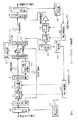
図1に本発明の基本構成を示す。
図1に示すフィードフォワード増幅器において、増幅器入力端子から高周波帯の信号(a)が入力されると、この入力信号は方向性結合器1により2系統に分配され、一方の信号が可変減衰器2、可変位相器3を介して方向性結合器4に入力される。方向性結合器4で2系統に分配された信号はそれぞれ遅延線路5及びピーク電力圧縮信号生成回路6を経て方向性結合器7で合成され、合成された信号は主増幅器8に入力され、主増幅器8の出力信号は方向性結合器11に入力される。また、方向性結合器1により2系統に分配された他方の信号は遅延線路9を経て方向性結合器11に入力される。
【0009】
方向性結合器11から出力される一方の歪成分を含んだ増幅信号(b)は遅延線路12を経て方向性結合器16に入力され、主増幅器8と遅延線路9の出力信号が逆相合成された他方の信号(c)は可変減衰器13、可変位相器14、補助増幅器15を経て方向性結合器16に入力される。
さらに、遅延線路12と補助増幅器15の出力信号は方向性結合器16により逆相合成された出力信号(d)が増幅器出力端子より出力される。
【0010】
ピーク電力またはピーク対平均電力比を圧縮する回路は、主増幅器入力側に設けられる。図1では、ピーク電力圧縮信号生成回路6Aとして示す。ピーク対平均電力比圧縮信号生成回路6Bについても図1と同様である。
図2に主増幅器入力信号ベクトルを示す。
図2の線形信号伝達経路ベクトル(遅延線路5出力信号)に対して、ほぼ逆位相になるピーク電力圧縮ベクトル(ピーク電力圧縮信号生成回路6出力信号)を生成する。この合成ベクトルが主増幅器入力信号ベクトル(方向性結合器7出力信号)となる。
【0011】
上記圧縮回路は、フィードフォワード増幅器入力信号を方向性結合器4または電力分配器等で検出し、その位相を反転し、所定の帯域に周波数変換して、方向性結合器7または電力分配器を介して主増幅器8入力経路にピーク電力またはピーク対平均電力比圧縮信号を注入する。これにより、主増幅器入力信号は、上記圧縮回路で生成される信号によりピーク電力またはピーク対平均電力比が圧縮され、主増幅器の出力バックオフを軽減できる。例えば、ピーク電力を3dB圧縮できれば、出力バックオフを3dB圧縮できる。ピーク電力またはピーク対平均電力比圧縮回路にて注入した信号は、歪除去ループにて検出し、等遅延、等振幅、逆位相になるように補助増幅器15を含む歪除去回路の歪注入経路にて調整し、主増幅器の出力経路に注入する。これにより、主増幅器の発生する非線形歪成分とともにピーク電力またはピーク対平均電力比を圧縮する信号を除去する。これにより、フィードフォワード増幅器は従来の歪補償能力を保持しつつ主増幅器の出力バックオフを軽減できる。
【0012】
図3にピーク電力圧縮信号を異なる周波数帯域に注入する例にて本発明の原理を説明する。
図3ではピーク電力圧縮信号の例を示すが、ピーク対平均電力比圧縮信号の場合も同様である。
図3(a)にフィードフォワード増幅器入力信号のスペクトルを示す。図3(b)に入力された送信信号からピーク電力圧縮回路にて生成されたピーク電力圧縮信号を送信信号と異なる帯域に注入したスペクトルを示す。このように、主増幅器入力時点において、送信信号とピーク電力圧縮信号のスペクトルは互いに干渉していない。図3(c)に主増幅器出力のスペクトルを示す。図3(c)から主増幅器の相互変調歪みによりそれぞれの信号の帯域外漏洩電力が生じる。また、それぞれの信号波による高次の非線形歪成分も同様にあるが、図3(c)では送信信号波近傍のみとして高次の非線形歪成分を除外している。図3(d)に歪検出回路にて検出され、可変位相器13、可変減衰器14、補助増幅器15を経たスペクトルを示す。歪検出回路にて、送信信号以外のスペクトル成分が検出されることが図3(c)と(d)からわかる。補助増幅器出力を歪除去回路の主増幅器出力経路に対して等振幅、等遅延、逆位相になるように歪注入経路の可変減衰器13と可変位相器14を制御する。調整された補助増幅器出力を主増幅器出力経路に注入する、すなわち、方向性結合器16で逆相合成することで、図3(e)のように主増幅器により発生する非線形歪成分を抑圧し、かつ主増幅器入力で注入したピーク電力圧縮信号を除去できる。
【0013】
図4にピーク電力圧縮信号またはピーク対平均電力比圧縮信号を送信信号と同一帯域に注入する例を示す。
図4ではピーク電力圧縮信号の例を示すが、ピーク対平均電力比圧縮信号の場合も同様である。図4(a)にフィードフォワード増幅器入力信号のスペクトルを示す。図4(b)に入力された送信信号からピーク電力圧縮信号生成回路6Aにて生成されたピーク電力圧縮信号を送信信号と同一帯域に注入したスペクトルを示す。図4(c)に主増幅器出力のスペクトルを示す。図4(c)から主増幅器の相互変調歪みによりそれぞれの信号の帯域外漏洩電力が生じる。また、それぞれの信号波による高次の非線形歪成分も同様にあるが、図4(c)では送信信号波近傍のみとして高次の非線形歪成分を除外している。図4(d)に歪検出回路にて検出され、可変位相器13、可変減衰器14、補助増幅器15を経たスペクトルを示す。歪検出回路にて、送信信号以外のスペクトル成分が検出されることが図4(c)と(d)からわかる。補助増幅器出力を歪除去回路の主増幅器出力経路に対して等振幅、等遅延、逆位相になるように歪注入経路の可変減衰器と可変位相器を制御する。調整された補助増幅器出力を主増幅器出力経路に注入する、すなわち、方向性結合器16で逆相合成することで、図4(e)のように主増幅器により発生する非線形歪成分を抑圧し、かつ主増幅器入力で注入されたピーク電力圧縮信号を除去できる。
【0014】
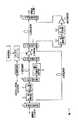
図5にパイロット信号を用いたフィードフォワード増幅器の基本構成を示す。
図5において、第一パイロット信号発生器21で発生させた第一パイロット信号を第一パイロット注入器22で歪検出回路に注入すると共に歪除去回路の第一パイロット抽出器23で第一パイロット信号を抽出し、第一レベル検出器24にてレベル検出をし、第一制御器25により可変減衰器2、可変位相器3を制御して第一レベル検出器24の検出レベルが最小となるように制御する。同様に、第二パイロット信号発生器31で発生させた第二パイロット信号を第二パイロット注入器32で主増幅器8に注入すると共に歪除去回路の第二パイロット抽出器33で第二パイロット信号を抽出し、第二レベル検出器34にてレベル検出をし、第二制御器35により可変減衰器13、可変位相器14を制御して第二レベル検出器34の検出レベルが最小となるように制御する。
【0015】
フィードフォワード増幅器の非線形歪補償量は、歪検出回路と歪除去回路の平衡度に依存する。その調整等の精度は、特公平7−77330号公報(特願昭63−23574号)「フィードフォワード増幅器の自動調整回路」に示されている。例えば、30dB以上の歪圧縮量を得るための位相及び振幅偏差は、それぞれ±2度以内及び±0.3dB以内であり、歪検出回路及び歪除去回路の平衡度及び調整の完全性について厳しい条件が要求されている。この平衡度を達成する方法として、パイロット信号を用いた歪検出回路と歪除去回路の自動調整方法が知られている(特公平7−77330号公報)。この方法を用いた装置(野島俊雄、楢橋祥一、「移動通信用超低歪多周波共通増幅器」、電子情報通信学会無線通信システム研究会技術報告、RCS90-4、1990)により、パイロット信号を用いて歪検出回路と歪除去回路の平衡を達成できることが知られている。本発明は、送信信号を遅延線路5を用いて線形に伝達する。これによりピーク電力圧縮信号生成回路6Aまたはピーク対平均電力比圧縮信号生成回路6Bによる送信信号に対する時間的な伝送特性の変動はない。よって、主増幅器8入力にピーク電力圧縮信号またはピーク対平均電力比圧縮信号を挿入しても、何らパイロット信号を用いた歪検出回路の平衡を達成する方法に影響を与えない。また、パイロット信号を含めてピーク電力圧縮信号生成回路またはピーク対平均電力比圧縮信号生成回路にてそれぞれの圧縮信号を送信信号に注入してもパイロット信号自身は除去されない。これは、本発明による回路が主増幅器入力信号のピーク電力またはピーク対平均電力比を圧縮するためである。また、ピーク電力圧縮回路またはピーク対平均電力圧縮回路の入力側にパイロット信号用ノッチフィルタ等を用意することでパイロット信号除去を回避できる。
(実施例)
図6に第一実施例を示す。
第一実施例は、トーン信号によるピーク電力圧縮回路のみを示す。可変位相器出力信号は、方向性結合器4により遅延線路5で構成される線形信号伝達経路とピーク電力圧縮信号生成回路6Aで構成されるピーク電力圧縮信号生成経路に分配される。ピーク電力圧縮信号生成回路6Aは、レベル識別回路6−1、ピーク電力検出回路6−2、低周波発振器6−3、周波数変換器6−4、可変位相器6−5、可変増幅器6−6の従属構成である。レベル識別回路6−1は、入力信号の振幅の瞬時値を観測する。観測された瞬時値は、事前にレベル識別回路に設定されている閾値と比較し、閾値以上の場合にピーク電力検出回路に振幅の瞬時値を伝達する。それ以外では、瞬時値を伝達しない。ピーク電力検出回路は、レベル識別回路出力から検出した入力信号のベクトルを検出する。この時、ピーク電力検出回路入力信号を直交検波し、入力信号の振幅値と位相値を検出する。検出された振幅値と位相値は低周波発振器6−3に入力される。低周波発振器6−3は、振幅値と位相値を設定できるシンセサイザで構成される。ここで、可変位相器出力信号を抑制するために位相値をほぼ逆位相になるように設定する。これにより、ピーク電力を圧縮するベクトルを生成できる。シンセサイザ出力は、周波数変換器6−4にて所定の帯域に周波数変換される。この時、増幅器入力信号と同一帯域または異なる帯域に周波数変換する。周波数変換されたピーク電力圧縮信号は、制御された可変位相器6−5と可変増幅器6−6で信号の振幅と位相の最終調整を行ない、電力合成・分配器7−1にて主増幅回路入力信号に注入される。可変増幅器6−6は、可変減衰器であっても同様のピーク電力圧縮効果が得られる。制御経路においては、可変位相器出力信号を電力合成・分配器7−1または方向性結合器で分配した信号をレベル識別回路6−11にて振幅の瞬時値を識別し、事前に設定されている閾値以上の場合にピーク電力検出回路6−12にて直交検波を行ない、制御回路6−13にて適応アルゴリズムにより段階的に行なう。制御回路6−13は、マイクロコンピュータで構成され、摂動法、最小自乗推定アルゴリズムなどで可変位相器と可変増幅器を制御する。
【0016】
本発明により、ピーク電力を適応的に圧縮できるため、主増幅器の出力バックオフを軽減できる。これにより、主増幅器の高効率増幅を可能にできる。例えば、PAPR(peak to average power ratio)を10dBの入力信号において、ピーク電力を4dB圧縮すれば、主増幅器入力信号のPAPRは6dBとなる。これにより、ピーク電力圧縮以前に出力バックオフ10dBが6dBにできる。この4dBの軽減により増幅効率への影響は、主増幅器をA級バイアス、飽和出力で最大ドレイン効率、最大ドレイン効率を50%、出力バックオフの定義を1dB利得圧縮点と動作点との差とすれば、本発明を適用する以前のドレイン効率が約4%に対して、本発明によりドレイン効率を約10%にできる。このように、ピーク電力を完全に圧縮しなくても本発明は効果がある。この時、帯域外漏洩電力及び符号間干渉等は全く生じない。
【0017】
図7に第二実施例を示す。
第二実施例は、周波数拡散されたピーク電力圧縮信号の生成方法において、これまでの低周波発振器6−3で生成した信号を特定の符号を用いて変調する。これにより、可変位相器及び可変増幅器の制御に用いる増幅回路入力信号のピーク電力の検出を容易にできる。低周波発振器6−3による圧縮信号ベクトルは、雑音等の影響を受けると容易に振幅と位相変化を受けやすい。第二実施例は、ピーク電力圧縮信号の安定性を向上するために、PN系列(pseudo random noise)等の特定の符号を符号発生器6−20で発生し、変調回路6−21にて低周波発振器で発生したピーク電力圧縮信号と符号発生器で発生した符号を乗算等の信号処理により変調を行なう。変調された信号は、周波数変換器6−4、可変位相器6−5、可変増幅器6−6を経て主増幅器入力段に注入される。また、注入後のピーク電力をモニタする経路では、レベル識別回路6−11にてピーク電力を観測し、ピーク電力検出回路6−12でピーク電力を可変位相器6−5と可変増幅器6−6の制御量を検出し、制御回路6−13で制御する。この時、ピーク電力検出回路は、符号発生器で生成する符号と同一の符号を用いて入力信号を復調する。これにより、ピーク電力圧縮信号の安定性を向上できる。
【0018】
図8に、直交検波器を用いたピーク対平均電力比を圧縮する第三実施例を示す。可変位相器出力信号は、方向性結合器4により遅延線路5で構成される線形信号伝達経路とピーク対平均電力比圧縮信号生成回路6Bで構成されるピーク対平均電力比圧縮信号生成経路に分配される。ピーク対平均電力比圧縮信号生成回路6Bは、直交検波器6−30、位相反転回路6−31、周波数変換器6−32、可変位相器6−33、可変増幅器6−34の従属構成である。直交検波器6−30は、入力信号を直交検波し、ベクトルを観測する。観測されたベクトルは、位相反転回路6−31にて、可変位相器出力信号を抑圧するために位相値をほぼ逆位相になるように設定する。これにより、ピーク対平均電力比を圧縮するベクトルを生成できる。位相反転回路出力は、周波数変換器6−32にて所定の帯域に周波数変換される。この時、増幅器入力信号と同一帯域または異なる帯域に周波数変換する。周波数変換されたピーク対平均電力比圧縮信号は、制御された可変位相器6−33と可変増幅器6−34で信号の振幅と位相の最終調整を行ない、電力合成・分配器7−1にて主増幅器入力信号に注入される。可変増幅器6−34は、可変減衰器であっても同様な効果が得られる。制御経路においては、主増幅器入力信号を電力合成・分配器7−1または方向性結合器で分配した信号をピーク対平均電力比検出回路6−35にてピーク電圧と平均電圧またはピーク電力と平均電力の瞬時値を識別し、事前に設定されている閾値以上の場合に直交検波を行ない、制御回路6−36にて可変位相器6−33、可変増幅器6−34の制御を適応アルゴリズムにより段階的に行なう。制御回路6−36は、マイクロコンピュータで構成され、摂動法、最小自乗推定アルゴリズムなどで可変位相器6−33と可変増幅器6−34を制御する。可変増幅器6−34については、可変減衰器であっても同様のピーク対平均電力比圧縮効果を得ることができる。
【0019】
図9に第4実施例を示す。
図9は、図8の構成のうち、ピーク対平均電力比圧縮信号生成経路の直交検波器を包絡線検波器6−40で構成する。この方法の利点は、ピーク対平均電力比検出回路の構成を簡易にできることである。
上記第1から第4実施例において、主増幅器に飽和増幅器を使用してもよい。一般にフィードフォワード増幅器には、線形増幅器をよく使用する。本発明のピーク電力圧縮回路またはピーク対平均電力比圧縮回路にて、主増幅器入力信号が等価的に定包絡化されるため、主増幅器に飽和増幅器を適用できる。これにより、従来の線形増幅器に比べて、ドレイン効率のきわめて高い飽和増幅器を使用できる。ドレイン効率が高いため、放熱板等の装置規模の削減と、簡易な増幅回路の調整など、設置性、経済性にすぐれた電力増幅器を構成できる。
【0020】
図10に第5実施例を示す。
本発明は、ドレイン電圧制御等の高効率増幅技術と組み合わせてもフィードフォワード増幅器において同様の高効率増幅と線形増幅を達成することができる。これは、主増幅器を高効率化する技術と、本発明により主増幅器の出力バックオフを軽減することで高効率化する技術が互いに独立しているためである。また、それらの技術を同時に用いることにより、相乗効果によりさらなる高効率増幅を達成することができる。特に、主増幅器のドレイン電圧をDC/DCコンバータで制御することによりCDMA(code division multiple access)無線通信における送信電力制御時の高効率化を行ない、かつ本発明により主増幅器の出力バックオフを低減することでフィードフォワード増幅器全体の高効率化が可能になる。
【0021】
上記第5実施例ではFETのドレイン電圧のみを制御したが、ゲート電圧を制御しても同様の効果が得られることが容易にいえる。また、ドレイン電圧とゲート電圧を同時に用いて制御しても同様の効果が得られる。
【0022】
【発明の効果】
以上説明したように本発明は、以下の効果を奏する。
(1)フィードフォワード増幅器の非線形歪補償能力を損なうことなく、高効率増幅が可能になる。
(2)送信側で完結しているため、受信側での処理を必要としない。
(3)簡易な回路構成で実現が可能である。
(4)飽和増幅器を適用でき、高効率増幅による装置の小型化、経済化を可能 にできる。
(5)主増幅器の高効率化技術と組み合わせることにより相乗効果が得られる。
【図面の簡単な説明】
【図1】 本発明の基本構成を示す図。
【図2】 主増幅器入力ベクトルをを説明する図。
【図3】 本発明のピーク電力圧縮信号またはピーク対平均電力比圧縮信号を異なる周波数帯域に注入する例を示す図。
【図4】 本発明のピーク電力圧縮信号またはピーク対平均電力比圧縮信号を同一周波数帯域に注入する例を示す図。
【図5】パイロット信号を用いたフィードフォワード増幅器の構成例を示す図。
【図6】 第1実施例であるトーン信号によるピーク電力圧縮回路の構成例を示す図。
【図7】 実施例である周波数拡散されたピーク電力圧縮回路の構成例を示す図。
【図8】 第3実施例である直交検波器を用いたピーク電力圧縮回路の構成例を示す図。
【図9】 第4実施例である包絡線検波器を用いたピーク電力圧縮回路の構成例を示す図。
【図10】 第5実施例であるドレイン電圧制御を用いたピーク電力圧縮回路の構成例を示す図。[0001]
BACKGROUND OF THE INVENTION
The present invention relates to improvement in power efficiency of a feedforward amplifier mainly used in a high frequency band.
[0002]
[Prior art]
In recent years, miniaturization, economy, and low power consumption of wireless devices have been demanded. The same applies to a mobile radio base station apparatus using a feedforward amplifier. In order to achieve low power consumption of the feedforward amplifier, it is essential to increase the efficiency of the main amplifier and the auxiliary amplifier. As a result, it is possible to reduce the size of the heat dissipation plate of the amplifier, and as a result, it is possible to reduce the size of the wireless device.
[0003]
The efficiency of the main amplifier can be increased by a push-pull circuit under a class B bias condition. Nonlinear distortion occurring in the main amplifier can be compensated by a conventional feedforward amplifier. For example, according to the literature (Toshio Nojima, Shoichi Takahashi, “Ultra Low Distortion Multi-Frequency Common Amplifier for Mobile Communication”, IEICE Technical Committee on Radio Communication Systems, RCS90-4, 1990), the saturation output of the main amplifier Is 100 W, the saturation output of the auxiliary amplifier is 1/8 of the saturation output of the main amplifier, the frequency is 1.5 GHz band, and GaAs MESFET (metal semiconductor field effect transistor) is used for the semiconductor amplifier elements of the main amplifier and the auxiliary amplifier. The drain efficiency of the feedforward amplifier is about 5% when the drain voltage of the MESFET of the main amplifier is 12V, the drain current is 20A, the drain voltage of the auxiliary amplifier MESFET is 12V, and the drain current is 5A. It becomes the following. When a high-efficiency amplifier circuit is used for the class B push-pull or the like as the main amplifier and a class A amplifier circuit is used as the auxiliary amplifier, a drain efficiency of about 10% or less can be obtained.
[0004]
Further, to improve the power efficiency of the feedforward amplifier, it is necessary to further improve the drain efficiency of the main amplifier. Up to now, as a method of performing high-efficiency amplification while achieving linearity of the amplifier, there has been known a method for improving the efficiency of the amplifier by the drain voltage control method (Koji Chiba, Toshio Nojima, Shigeru Kaori, “Bidirectional Feed Type drain voltage control amplifier (BDF-DVCA) ", IEICE Technical Report on Radio Systems, RCS89-33, 1989.). This method increases drain efficiency by equivalently reducing the output back-off of the amplifier.
[0005]
[Problems to be solved by the invention]
In the drain voltage control method, power supplied to a semiconductor such as an FET is modulated. For example, in a base station power amplifier with a transmission output of 100 W, if the drain efficiency of the final stage FET is 50% (class A bias theoretical maximum value), the power supplied to the final stage FET is 200 W. In this case, DC power control by the drain voltage control method is performed for 200 W. If the drain voltage of the FET is 10V, the drain current is 20A. Such a large current is controlled by an FET or the like. However, the higher the output power amplifier, the more difficult it is to perform drain voltage control with low loss due to the loss of the on-resistance of the FET that controls a large current.
[0006]
The problem to be solved by the present invention is to achieve high efficiency of the feedforward amplifier by reducing the output back-off of the main amplifier while having a distortion compensation capability equal to or higher than that of the conventional feedforward amplifier. .
[0007]
[Means for Solving the Problems]
In order to solve the above problems, the following means are used.
(1) According to the invention of
(2)Then , the peak power of the main amplifier input signal is detected, a signal for compressing the peak power is generated, and injected to the main amplifier input. Thereby, the peak power can always be compressed without depending on the nature of the input signal. Also, a complete circuit configuration on the transmission side can be realized.
(3) According to the invention of claim2 , the circuit for compressing the peak-to-average power ratio of the main amplifier input signal of the feedforward amplifier is provided on the main amplifier input side. This compresses the peak to average power ratio of the main amplifier input signal and reduces the output backoff of the main amplifier.
(4)Then , the peak-to-average power ratio of the main amplifier input signal is detected, a signal for compressing the peak-to-average power ratio is generated, and injected into the main amplifier input. As a result, the peak-to-average power ratio can always be compressed without depending on the nature of the input signal. Also, a complete circuit configuration on the transmission side can be realized.
(5) According to the invention of
(6) According to the invention of
(7) According to the invention of claim5 , in the feedforward amplifier of claim2 , the signal for compressing the peak-to-average power ratio is frequency-converted to the same band as the feedforward amplifier input signal, and the output backoff of the main amplifier Reduce.
(8) According to the invention of claim6 , in the feedforward amplifier of claim2 , the signal for compressing the peak-to-average power ratio is frequency-converted to a band different from the input signal of the feedforward amplifier, and the output backoff of the main amplifier Reduce.
(9) According tothe first proposed example , in the feedforward amplifier according to
(10) According tothe second proposal, in the feedforward amplifier according to
(11) According tothe third proposal, in the feedforward amplifier according to
[0008]
DETAILED DESCRIPTION OF THE INVENTION
FIG. 1 shows the basic configuration of the present invention.
In the feedforward amplifier shown in FIG. 1, when a signal (a) in a high frequency band is input from an amplifier input terminal, this input signal is distributed to two systems by a
[0009]
The amplified signal (b) including one distortion component output from the
Further, the output signal (d) obtained by reverse-phase synthesis of the output signals of the delay line 12 and the
[0010]
A circuit for compressing the peak power or peak-to-average power ratio is provided on the main amplifier input side. In FIG. 1, it is shown as a peak power compressed
FIG. 2 shows the main amplifier input signal vector.
A peak power compression vector (peak power compression signal generation circuit 6 output signal) having an approximately opposite phase is generated with respect to the linear signal transmission path vector (delay line 5 output signal) of FIG. This combined vector becomes the main amplifier input signal vector (directional coupler7 output signal).
[0011]
The compression circuit detects the feedforward amplifier input signal with the
[0012]
The principle of the present invention will be described with reference to FIG. 3 in which the peak power compression signal is injected into different frequency bands.
Although FIG. 3 shows an example of the peak power compressed signal, the same applies to the peak-to-average power ratio compressed signal.
FIG. 3A shows the spectrum of the feedforward amplifier input signal. FIG. 3B shows a spectrum in which the peak power compressed signal generated by the peak power compression circuit from the input transmission signal is injected into a band different from the transmission signal. Thus, the spectrum of the transmission signal and the peak power compression signal do not interfere with each other at the time of input to the main amplifier. FIG. 3 (c) shows the spectrum of the main amplifier output. From FIG. 3 (c), out-of-band leakage power of each signal occurs due to the intermodulation distortion of the main amplifier. The same applies to the higher-order nonlinear distortion components due to the respective signal waves, but in FIG. 3C, the higher-order nonlinear distortion components are excluded only in the vicinity of the transmission signal wave. FIG. 3 (d) shows a spectrum detected by the distortion detection circuit and passed through the
[0013]
FIG. 4 shows an example in which the peak power compressed signal or the peak-to-average power ratio compressed signal is injected into the same band as the transmission signal.
Although FIG. 4 shows an example of the peak power compressed signal, the same applies to the peak-to-average power ratio compressed signal. FIG. 4 (a) shows the spectrum of the feedforward amplifier input signal. FIG. 4B shows a spectrum in which the peak power compressed signal generated by the peak power compressed
[0014]
Figure 5 shows the basic configuration of a feedforward amplifier using apilot signal.
In FIG. 5, the first pilot signal generated by the first
[0015]
The nonlinear distortion compensation amount of the feedforward amplifier depends on the degree of balance between the distortion detection circuit and the distortion removal circuit. The accuracy of such adjustment is shown in Japanese Patent Publication No. 7-77330 (Japanese Patent Application No. 63-23574) “Automatic Adjustment Circuit of Feedforward Amplifier”. For example, the phase and amplitude deviation for obtaining a distortion compression amount of 30 dB or more are within ± 2 degrees and ± 0.3 dB, respectively, and severe conditions are imposed on the degree of balance and completeness of adjustment of the distortion detection circuit and the distortion removal circuit. Is required. As a method for achieving this balance, an automatic adjustment method for a distortion detection circuit and a distortion removal circuit using a pilot signal is known (Japanese Patent Publication No. 7-77330). By using this method (Toshio Nojima, Shoichi Takahashi, “Ultra Low Distortion Multi-frequency Common Amplifier for Mobile Communications”, IEICE Technical Report on Radio Communication Systems, RCS90-4, 1990) It is known that it can be used to achieve a balance between the distortion detection circuit and the distortion removal circuit. In the present invention, the transmission signal is transmitted linearly using the delay line 5. As a result, there is no temporal variation in transmission characteristics with respect to the transmission signal by the peak power compression
(Example)
FIG. 6 shows a first embodiment.
The first embodiment shows only a peak power compression circuit using a tone signal. The variable phase shifter output signal is distributed by the
[0016]
According to the present invention, the peak power can be adaptively compressed, so that the output back-off of the main amplifier can be reduced. Thereby, high efficiency amplification of the main amplifier can be realized. For example, if the peak power is compressed by 4 dB in an input signal with a PAPR (peak to average power ratio) of 10 dB, the PAPR of the main amplifier input signal becomes 6 dB. This allows the output backoff 10 dB to be 6 dB before peak power compression. The 4dB reduction affects amplification efficiency. The main amplifier is class A bias, the maximum drain efficiency with saturated output, the maximum drain efficiency is 50%, and the output back-off is defined as the difference between the 1 dB gain compression point and the operating point. Then, the drain efficiency before the application of the present invention is about 4%, and the drain efficiency can be made about 10% by the present invention. Thus, the present invention is effective even if the peak power is not completely compressed. At this time, out-of-band leakage power and intersymbol interference do not occur at all.
[0017]
FIG. 7 shows a second embodiment.
The second embodiment modulates a signal generated by a conventional low frequency oscillator 6-3 using a specific code in a method of generating a frequency-spread peak power compressed signal. Thereby, it is possible to easily detect the peak power of the input signal of the amplifier circuit used for controlling the variable phase shifter and the variable amplifier. The compressed signal vector by the low-frequency oscillator 6-3 is easily subjected to changes in amplitude and phase when affected by noise or the like. In the second embodiment, in order to improve the stability of the peak power compression signal, a specific code such as a PN sequence (pseudo random noise) is generated by the code generator 6-20 and low by the modulation circuit 6-21. The peak power compression signal generated by the frequency oscillator and the code generated by the code generator are modulated by signal processing such as multiplication. The modulated signal is injected into the main amplifier input stage through the frequency converter 6-4, the variable phase shifter 6-5, and the variable amplifier 6-6. In the path for monitoring the peak power after injection, the peak power is observed by the level identification circuit 6-11, and the peak power is monitored by the peak power detection circuit 6-12 and the variable phase shifter 6-5 and the variable amplifier 6-6. Is controlled by the control circuit 6-13. At this time, the peak power detection circuit demodulates the input signal using the same code as the code generated by the code generator. Thereby, the stability of the peak power compression signal can be improved.
[0018]
FIG. 8 shows a third embodiment for compressing the peak-to-average power ratio using a quadrature detector. The variable phase shifter output signal is distributed by the
[0019]
FIG. 9 shows a fourth embodiment.
In FIG. 9, the quadrature detector of the peak-to-average power ratio compressed signal generation path in the configuration of FIG. 8 is configured by an envelope detector 6-40. The advantage of this method is that the configuration of the peak-to-average power ratio detection circuit can be simplified.
In the first to fourth embodiments, a saturation amplifier may be used as the main amplifier. In general, a linear amplifier is often used as a feedforward amplifier. In the peak power compression circuit or peak-to-average power ratio compression circuit of the present invention, the main amplifier input signal is equivalently constant enveloped, so that a saturation amplifier can be applied to the main amplifier. Thereby, it is possible to use a saturation amplifier having extremely high drain efficiency as compared with the conventional linear amplifier. Since the drain efficiency is high, it is possible to configure a power amplifier that is excellent in installation and economy, such as reduction in the scale of a heat sink and the like and simple adjustment of an amplifier circuit.
[0020]
FIG. 10 shows a fifth embodiment.
The present invention can achieve the same high efficiency amplification and linear amplification in the feedforward amplifier even when combined with a high efficiency amplification technique such as drain voltage control. This is because the technology for improving the efficiency of the main amplifier and the technology for improving the efficiency by reducing the output back-off of the main amplifier according to the present invention are independent of each other. Moreover, by using these techniques simultaneously, a further highly efficient amplification can be achieved by a synergistic effect. In particular, the drain voltage of the main amplifier is controlled by a DC / DC converter to improve the efficiency during transmission power control in CDMA (code division multiple access) wireless communications, and the output back-off of the main amplifier is reduced by the present invention. This makes it possible to increase the efficiency of the entire feedforward amplifier.
[0021]
Although only the drain voltage of the FET is controlled in the fifth embodiment, it can be easily said that the same effect can be obtained even if the gate voltage is controlled. Further, the same effect can be obtained by controlling the drain voltage and the gate voltage at the same time.
[0022]
【The invention's effect】
As described above, the present invention has the following effects.
(1) High-efficiency amplification is possible without impairing the nonlinear distortion compensation capability of the feedforward amplifier.
(2) Since processing is completed on the transmission side, processing on the reception side is not required.
(3) Realization is possible with a simple circuit configuration.
(4) Saturation amplifiers can be applied, and the device can be made smaller and more economical by high-efficiency amplification.
(5) A synergistic effect can be obtained by combining with the high efficiency technology of the main amplifier.
[Brief description of the drawings]
FIG. 1 is a diagram showing a basic configuration of the present invention.
FIG. 2 is a diagram illustrating a main amplifier input vector.
FIG. 3 is a diagram showing an example in which the peak power compression signal or the peak-to-average power ratio compression signal of the present invention is injected into different frequency bands.
FIG. 4 is a diagram showing an example in which a peak power compression signal or a peak-to-average power ratio compression signal of the present invention is injected into the same frequency band.
5 is a diagram showing a configuration example of a feedforward amplifier using apilot signal.
FIG. 6 is a diagram illustrating a configuration example of a peak power compression circuit using a tone signal according to the first embodiment.
FIG. 7 is a diagram illustrating a configuration example of a frequency-spread peak power compression circuit according to an embodiment.
FIG. 8 is a diagram showing a configuration example of a peak power compression circuit using a quadrature detector according to a third embodiment.
FIG. 9 is a diagram showing a configuration example of a peak power compression circuit using an envelope detector according to a fourth embodiment.
FIG. 10 is a diagram illustrating a configuration example of a peak power compression circuit using drain voltage control according to a fifth embodiment.
Claims (6)
Translated fromJapanese歪検出ループの主増幅器入力側にフィードフォワード増幅器入力信号のピーク電力を圧縮するピーク電力圧縮回路を歪検出ループ内に備え、
上記ピーク電力圧縮回路は、
主増幅器入力信号を線形に伝達する線形信号伝達経路と、
所定値以上の主増幅器入力信号のピーク電力を検出し、その検出した信号を用いて該ピーク電力に対しほぼ逆位相のピーク電力圧縮信号を生成し、そのピーク電力圧縮信号の振幅を調整する振幅調整手段と、位相を調整する位相調整手段を備えるピーク電力圧縮信号生成経路と、
上記二つの経路を電力合成し、主増幅器入力と制御経路に分配する電力合成・分配手段と、
該電力合成・分配手段で制御経路に分配された信号により上記主増幅器に入力された信号のピーク電力を検出し、そのピーク電力を予め決めた値に圧縮するように該ピーク電力圧縮信号生成経路の振幅調整手段と位相調整手段を制御する制御手段を備える制御経路により構成されることを特徴とするフィードフォワード増幅器。In a feedforward amplifier having a distortion detection loop of a main amplifier, and a distortion elimination loop that cancels the distortion component by amplifying the detected distortion component by an auxiliary amplifier and then injecting the distortion component again to the main amplifier output,
The distortion detection loop includes a peak power compression circuit for compressing the peak power of the feedforward amplifier input signal on the main amplifier input side of thedistortion detection loop .
The peak power compression circuit is
A linear signal transmission path for linearly transmitting the main amplifier input signal;
Amplitude that detects the peak powerof the main amplifier input signal that isgreater than or equal to a predetermined value , generatesa peak power compressed signalthat is substantially in phase with the peak power using the detected signal, and adjusts the amplitude of thepeak power compressed signal A peak power compression signal generation path comprising an adjustment means and a phase adjustment means for adjusting the phase;
Power combining / distributing means for combining the power of the two paths and distributing the power to the main amplifier input and the control path;
The peak power compression signal generation path detects the peak power ofthe signal input to the main amplifier based on the signal distributed to the control path by the power combining / distribution meansand compresses the peak power to apredetermined value. A feedforward amplifier comprising a control path including control means for controlling the amplitude adjusting means and the phase adjusting means.
歪検出ループの主増幅器入力側にフィードフォワード増幅器入力信号のピーク対平均電力比を圧縮するピーク対平均電力比圧縮回路を歪検出ループ内に備え、
上記ピーク対平均電力比圧縮回路は、
主増幅器入力信号を線形に伝達する線形信号伝達経路と、
主増幅器入力信号のピーク対平均電力比を検出し、その検出した信号を用いて該ピーク対平均電力比を圧縮する信号を生成し、その信号の振幅を調整する振幅調整手段と、位相を調整する位相調整手段を備えるピーク対平均電力比圧縮信号生成経路と、
上記二つの経路を電力合成し、主増幅器入力と制御経路に分配する電力合成・分配手段と、
該電力合成・分配手段で制御経路に分配された信号のピーク対平均電力比を検出し、そのピーク対平均電力比を圧縮するように該ピーク対平均電力比圧縮信号生成経路の振幅調整手段と位相調整手段を制御する制御手段を備える制御経路により構成されることを特徴とするフィードフォワード増幅器。In a feedforward amplifier having a distortion detection loop of a main amplifier, and a distortion elimination loop that cancels the distortion component by amplifying the detected distortion component by an auxiliary amplifier and then injecting the distortion component again to the main amplifier output,
A peak-to-average power ratio compression circuit that compresses the peak-to-average power ratio of the feedforward amplifier input signal on the main amplifier input side of thedistortion detection loop is provided in the distortion detection loop ,
The peak to average power ratio compression circuit is:
A linear signal transmission path for linearly transmitting the main amplifier input signal;
Detects the peak-to-average power ratio of the main amplifier input signal, generates a signal that compresses the peak-to-average power ratio using the detected signal, adjusts the amplitude of the signal, and adjusts the phase A peak-to-average power ratio compressed signal generation path comprising phase adjusting means for
Power combining / distributing means for combining the power of the two paths and distributing the power to the main amplifier input and the control path;
Amplitude adjusting means for detecting the peak-to-average power ratio of the signal distributed to the control path by the power combining / distributing means and compressing the peak-to-average power ratio so as to compress the peak-to-average power ratio; A feedforward amplifier comprising a control path including control means for controlling phase adjusting means.
ピーク電力圧縮信号生成経路にて生成した信号をフィードフォワード増幅器入力信号と同じ帯域に周波数変換して主増幅器入力経路に注入することを特徴とするフィードフォワード増幅器。The feed forward amplifier according to claim1 .
A feedforward amplifier characterized in that a signal generated in a peak power compression signal generation path is frequency-converted to the same band as a feedforward amplifier input signal and injected into a main amplifier input path.
ピーク電力圧縮信号生成経路にて生成した信号をフィードフォワード増幅器入力信号と異なる帯域に周波数変換して主増幅器入力経路に注入することを特徴とするフィードフォワード増幅器。The feed forward amplifier according to claim1 .
A feedforward amplifier characterized in that a signal generated in a peak power compression signal generation path is frequency-converted to a band different from that of a feedforward amplifier input signal and injected into a main amplifier input path.
ピーク対平均電力比圧縮信号生成経路にて生成した信号をフィードフォワード増幅器入力信号と同じ帯域に周波数変換して主増幅器入力経路に注入することを特徴とするフィードフォワード増幅器。The feedforward amplifier according to claim2 .
A feedforward amplifier characterized in that a signal generated in a peak-to-average power ratio compression signal generation path is frequency-converted into the same band as the feedforward amplifier input signal and injected into the main amplifier input path.
ピーク対平均電力比圧縮信号生成経路にて生成した信号をフィードフォワード増幅器入力信号と異なる帯域に周波数変換して主増幅器入力経路に注入することを特徴とするフィードフォワード増幅器。The feedforward amplifier according to claim2 .
A feedforward amplifier characterized in that a signal generated in a peak-to-average power ratio compressed signal generation path is frequency-converted to a band different from that of a feedforward amplifier input signal and injected into a main amplifier input path.
Priority Applications (5)
| Application Number | Priority Date | Filing Date | Title |
|---|---|---|---|
| JP2000146327AJP3877937B2 (en) | 2000-05-18 | 2000-05-18 | Feed forward amplifier |
| EP01111223AEP1158661B1 (en) | 2000-05-18 | 2001-05-15 | Feed-forward amplifier |
| US09/854,476US6392483B2 (en) | 2000-05-18 | 2001-05-15 | Feed-forward amplifier |
| DE60142382TDE60142382D1 (en) | 2000-05-18 | 2001-05-15 | Forward coupled amplifier |
| CN01117687.3ACN1220327C (en) | 2000-05-18 | 2001-05-16 | Feedforward amplifier |
Applications Claiming Priority (1)
| Application Number | Priority Date | Filing Date | Title |
|---|---|---|---|
| JP2000146327AJP3877937B2 (en) | 2000-05-18 | 2000-05-18 | Feed forward amplifier |
Publications (2)
| Publication Number | Publication Date |
|---|---|
| JP2001326538A JP2001326538A (en) | 2001-11-22 |
| JP3877937B2true JP3877937B2 (en) | 2007-02-07 |
Family
ID=18652704
Family Applications (1)
| Application Number | Title | Priority Date | Filing Date |
|---|---|---|---|
| JP2000146327AExpired - Fee RelatedJP3877937B2 (en) | 2000-05-18 | 2000-05-18 | Feed forward amplifier |
Country Status (5)
| Country | Link |
|---|---|
| US (1) | US6392483B2 (en) |
| EP (1) | EP1158661B1 (en) |
| JP (1) | JP3877937B2 (en) |
| CN (1) | CN1220327C (en) |
| DE (1) | DE60142382D1 (en) |
Families Citing this family (43)
| Publication number | Priority date | Publication date | Assignee | Title |
|---|---|---|---|---|
| GB9616142D0 (en) | 1996-08-01 | 1996-09-11 | Northern Telecom Ltd | Distribution network |
| EP1113637B1 (en)* | 1999-12-28 | 2006-04-05 | NTT DoCoMo, Inc. | Circuit for the compression of the dynamic range of a signal |
| US6630899B2 (en)* | 2000-07-20 | 2003-10-07 | Tripath Technology, Inc. | Scheme for maximizing efficiency of power amplifier under power backoff conditions |
| KR100547843B1 (en)* | 2001-07-13 | 2006-02-01 | 삼성전자주식회사 | Transmission power control device and method for mobile communication system |
| US6677817B2 (en)* | 2001-12-17 | 2004-01-13 | Powerwave Technologies, Inc. | Feed forward amplifier with amplifier stage failure detection using pilot tones |
| CA2476246C (en)* | 2002-02-14 | 2011-10-04 | Powerwave Technologies, Inc. | Feed forward rf power amplifier with high efficiency main amplifier and highly linear error amplifier |
| DE10206966B4 (en)* | 2002-02-19 | 2011-08-11 | Rohde & Schwarz GmbH & Co. KG, 81671 | Method for estimating gain factors of a CDMA signal |
| KR100459065B1 (en)* | 2002-07-25 | 2004-12-03 | 학교법인 포항공과대학교 | Linearization apparatus using peak-to-average power ratio reduction and expansion |
| US7209715B2 (en)* | 2002-07-30 | 2007-04-24 | Matsushita Electric Industrial Co., Ltd. | Power amplifying method, power amplifier, and communication apparatus |
| CA2442938A1 (en)* | 2002-09-30 | 2004-03-30 | Vcom Inc. | Method and apparatus for reducing the power consumption of the power amplifier used in a qam modulator |
| JP4657920B2 (en)* | 2002-11-14 | 2011-03-23 | 株式会社日立国際電気 | Distortion compensation circuit, distortion compensation signal generation method, and power amplifier |
| GB2402308B (en)* | 2003-05-28 | 2006-01-04 | Nokia Corp | Par reduction for edge clipper |
| US7129778B2 (en)* | 2003-07-23 | 2006-10-31 | Northrop Grumman Corporation | Digital cross cancellation system |
| US7042287B2 (en) | 2003-07-23 | 2006-05-09 | Northrop Grumman Corporation | System and method for reducing dynamic range and improving linearity in an amplication system |
| JP3910167B2 (en)* | 2003-09-25 | 2007-04-25 | 松下電器産業株式会社 | Amplifier circuit |
| KR101009778B1 (en)* | 2003-10-23 | 2011-01-19 | 삼성전자주식회사 | Power amplification device and method having high peak power to average power ratio |
| US7126422B2 (en)* | 2004-01-28 | 2006-10-24 | Ntt Docomo, Inc. | Multi-band feed-forward amplifier and adjustment method therefor |
| US7826435B1 (en)* | 2004-03-05 | 2010-11-02 | Zte (Usa) Inc. | Power control in OFDM and OFDMA wireless communication networks |
| US7157967B2 (en)* | 2004-03-11 | 2007-01-02 | Powerwave Technologies Inc. | System and method for control of loop alignment in adaptive feed forward amplifiers |
| US7327803B2 (en) | 2004-10-22 | 2008-02-05 | Parkervision, Inc. | Systems and methods for vector power amplification |
| US7355470B2 (en) | 2006-04-24 | 2008-04-08 | Parkervision, Inc. | Systems and methods of RF power transmission, modulation, and amplification, including embodiments for amplifier class transitioning |
| CN100576767C (en)* | 2005-06-03 | 2009-12-30 | 株式会社Ntt都科摩 | Feedforward Amplifier for Multiband |
| DE602006000131T2 (en)* | 2005-06-03 | 2008-07-03 | Ntt Docomo Inc. | Band selection-forward amplifier |
| US9106316B2 (en) | 2005-10-24 | 2015-08-11 | Parkervision, Inc. | Systems and methods of RF power transmission, modulation, and amplification |
| US8334722B2 (en) | 2007-06-28 | 2012-12-18 | Parkervision, Inc. | Systems and methods of RF power transmission, modulation and amplification |
| US20130078934A1 (en) | 2011-04-08 | 2013-03-28 | Gregory Rawlins | Systems and Methods of RF Power Transmission, Modulation, and Amplification |
| US7911272B2 (en) | 2007-06-19 | 2011-03-22 | Parkervision, Inc. | Systems and methods of RF power transmission, modulation, and amplification, including blended control embodiments |
| US7937106B2 (en) | 2006-04-24 | 2011-05-03 | ParkerVision, Inc, | Systems and methods of RF power transmission, modulation, and amplification, including architectural embodiments of same |
| US8031804B2 (en) | 2006-04-24 | 2011-10-04 | Parkervision, Inc. | Systems and methods of RF tower transmission, modulation, and amplification, including embodiments for compensating for waveform distortion |
| US7620129B2 (en) | 2007-01-16 | 2009-11-17 | Parkervision, Inc. | RF power transmission, modulation, and amplification, including embodiments for generating vector modulation control signals |
| JP4880502B2 (en)* | 2007-03-13 | 2012-02-22 | 日本無線株式会社 | Relay device |
| WO2008144017A1 (en) | 2007-05-18 | 2008-11-27 | Parkervision, Inc. | Systems and methods of rf power transmission, modulation, and amplification |
| WO2008156800A1 (en) | 2007-06-19 | 2008-12-24 | Parkervision, Inc. | Combiner-less multiple input single output (miso) amplification with blended control |
| US7778318B1 (en)* | 2007-08-15 | 2010-08-17 | Agilent Technologies, Inc. | OFDM gain compression measurement |
| JP4424418B2 (en) | 2007-12-26 | 2010-03-03 | トヨタ自動車株式会社 | Fuel cell system and fuel cell vehicle |
| US8755762B2 (en)* | 2008-08-05 | 2014-06-17 | Broadcom Corporation | RF receiver with oscillation based blocker |
| US7782141B2 (en)* | 2008-12-29 | 2010-08-24 | Texas Instruments Incorporated | Adaptive signal-feed-forward circuit and method for reducing amplifier power without signal distortion |
| US8447245B2 (en)* | 2010-01-22 | 2013-05-21 | Freescale Semiconductor, Inc. | Radio frequency transmitter having an amplifier with power supply modulation |
| KR20140034895A (en) | 2011-06-02 | 2014-03-20 | 파커비전, 인크. | Antenna control |
| KR101674415B1 (en)* | 2012-04-27 | 2016-11-09 | 삼성전자주식회사 | Mehtod and apparatus for controlling signal gain in digital signal processing system |
| CN106415435B (en) | 2013-09-17 | 2020-08-11 | 帕克维辛股份有限公司 | Method, apparatus, and system for presenting information-carrying time functions |
| CN104467718B (en)* | 2014-11-19 | 2017-05-17 | 天津光电通信技术有限公司 | Module circuit for compressing dynamic range of radio-frequency signals |
| US10944369B2 (en) | 2016-07-14 | 2021-03-09 | Telefonaktiebolaget Lm Ericsson (Publ) | Amplifier circuit and method for compensating an output signal provided at an output of the amplifier circuit |
Family Cites Families (8)
| Publication number | Priority date | Publication date | Assignee | Title |
|---|---|---|---|---|
| US4943783A (en)* | 1989-07-31 | 1990-07-24 | Nippon Telegraph And Telephone Corporation | Feed forward distortion correction circuit |
| US5638403A (en)* | 1995-04-28 | 1997-06-10 | Motorola, Inc. | Low-splatter peak-to-average signal reduction with interpolation |
| RU2142670C1 (en)* | 1995-11-16 | 1999-12-10 | Самсунг Электроникс Ко., Лтд. | Device for linear power amplification |
| US5760646A (en)* | 1996-03-29 | 1998-06-02 | Spectrian | Feed-forward correction loop with adaptive predistortion injection for linearization of RF power amplifier |
| US6175270B1 (en)* | 1998-03-05 | 2001-01-16 | Lucent Technologies Inc. | Method and apparatus for tailored distortion of a signal prior to amplification to reduce clipping |
| US6046635A (en)* | 1998-04-08 | 2000-04-04 | Powerwave Technologies, Inc. | Dynamic predistortion compensation for a power amplifier |
| EP1724917A1 (en)* | 1999-03-31 | 2006-11-22 | NTT Mobile Communications Network Inc. | Feedforward amplifier |
| US6211733B1 (en)* | 1999-10-22 | 2001-04-03 | Powerwave Technologies, Inc. | Predistortion compensation for a power amplifier |
- 2000
- 2000-05-18JPJP2000146327Apatent/JP3877937B2/ennot_activeExpired - Fee Related
- 2001
- 2001-05-15USUS09/854,476patent/US6392483B2/ennot_activeExpired - Lifetime
- 2001-05-15EPEP01111223Apatent/EP1158661B1/ennot_activeExpired - Lifetime
- 2001-05-15DEDE60142382Tpatent/DE60142382D1/ennot_activeExpired - Lifetime
- 2001-05-16CNCN01117687.3Apatent/CN1220327C/ennot_activeExpired - Fee Related
Also Published As
| Publication number | Publication date |
|---|---|
| EP1158661B1 (en) | 2010-06-16 |
| US6392483B2 (en) | 2002-05-21 |
| EP1158661A2 (en) | 2001-11-28 |
| DE60142382D1 (en) | 2010-07-29 |
| JP2001326538A (en) | 2001-11-22 |
| EP1158661A3 (en) | 2002-10-02 |
| US20010043118A1 (en) | 2001-11-22 |
| CN1325182A (en) | 2001-12-05 |
| CN1220327C (en) | 2005-09-21 |
Similar Documents
| Publication | Publication Date | Title |
|---|---|---|
| JP3877937B2 (en) | Feed forward amplifier | |
| US6621367B2 (en) | Signal power dynamic range compressing circuit and power amplifier using the same | |
| KR100362925B1 (en) | Feedforward amplifier | |
| US20100117726A1 (en) | Amplifier apparatus | |
| US20030184371A1 (en) | Power amplifier array with same type predistortion amplifier | |
| WO2005124994A1 (en) | High-efficiency amplifier | |
| CN108347226B (en) | Envelope tracking method, system and device | |
| KR20030011827A (en) | Method and apparatus for optimum biasing of cascaded mosfet radio-frequency devices | |
| JP4052834B2 (en) | Amplifier circuit | |
| Yang et al. | Optimization for error-canceling loop of the feedforward amplifier using a new system-level mathematical model | |
| JP3827130B2 (en) | Feed forward amplifier | |
| KR19990060622A (en) | Predistortion linearization device and method for adjusting individual orders of intermodulation signals | |
| US6999734B2 (en) | Nonlinear compensating circuit, base-station apparatus, and transmission power clipping method | |
| Farabegoli et al. | Advanced transmitters with combined crest factor reduction and digital predistortion techniques | |
| JP3848836B2 (en) | Signal power dynamic range compression circuit and power amplification circuit using the same | |
| JP2001339253A (en) | Amplifier | |
| JP3613447B2 (en) | Feedforward amplifier with double loop | |
| JP4014404B2 (en) | Distortion compensation circuit | |
| KR20050039063A (en) | Apparatus and method for improving the efficiency of power amplifier operating under a large peak-to-average ratio | |
| JP3513138B2 (en) | Communication terminal and its control circuit | |
| KR100370545B1 (en) | A high power type pre-distorting apparatus for reducing spurious signal in high frequency band linear power amplifier | |
| JP2001094359A (en) | Distortion compensation amplifier | |
| Thornton et al. | Improved design techniques for the realization of linear power amplifiers for wireless transmitters | |
| KR200223073Y1 (en) | A predistortion apparatus for correcting a non lenear characteristic of frequency mixer | |
| CN119010800A (en) | Power amplifying circuit, transmitting device and communication equipment |
Legal Events
| Date | Code | Title | Description |
|---|---|---|---|
| A977 | Report on retrieval | Free format text:JAPANESE INTERMEDIATE CODE: A971007 Effective date:20050629 | |
| A131 | Notification of reasons for refusal | Free format text:JAPANESE INTERMEDIATE CODE: A131 Effective date:20060328 | |
| A521 | Request for written amendment filed | Free format text:JAPANESE INTERMEDIATE CODE: A523 Effective date:20060529 | |
| RD03 | Notification of appointment of power of attorney | Free format text:JAPANESE INTERMEDIATE CODE: A7423 Effective date:20060529 | |
| TRDD | Decision of grant or rejection written | ||
| A01 | Written decision to grant a patent or to grant a registration (utility model) | Free format text:JAPANESE INTERMEDIATE CODE: A01 Effective date:20061017 | |
| A61 | First payment of annual fees (during grant procedure) | Free format text:JAPANESE INTERMEDIATE CODE: A61 Effective date:20061101 | |
| R150 | Certificate of patent or registration of utility model | Ref document number:3877937 Country of ref document:JP Free format text:JAPANESE INTERMEDIATE CODE: R150 Free format text:JAPANESE INTERMEDIATE CODE: R150 | |
| FPAY | Renewal fee payment (event date is renewal date of database) | Free format text:PAYMENT UNTIL: 20091110 Year of fee payment:3 | |
| FPAY | Renewal fee payment (event date is renewal date of database) | Free format text:PAYMENT UNTIL: 20101110 Year of fee payment:4 | |
| R250 | Receipt of annual fees | Free format text:JAPANESE INTERMEDIATE CODE: R250 | |
| FPAY | Renewal fee payment (event date is renewal date of database) | Free format text:PAYMENT UNTIL: 20111110 Year of fee payment:5 | |
| R250 | Receipt of annual fees | Free format text:JAPANESE INTERMEDIATE CODE: R250 | |
| FPAY | Renewal fee payment (event date is renewal date of database) | Free format text:PAYMENT UNTIL: 20121110 Year of fee payment:6 | |
| R250 | Receipt of annual fees | Free format text:JAPANESE INTERMEDIATE CODE: R250 | |
| FPAY | Renewal fee payment (event date is renewal date of database) | Free format text:PAYMENT UNTIL: 20121110 Year of fee payment:6 | |
| FPAY | Renewal fee payment (event date is renewal date of database) | Free format text:PAYMENT UNTIL: 20131110 Year of fee payment:7 | |
| R250 | Receipt of annual fees | Free format text:JAPANESE INTERMEDIATE CODE: R250 | |
| R250 | Receipt of annual fees | Free format text:JAPANESE INTERMEDIATE CODE: R250 | |
| R250 | Receipt of annual fees | Free format text:JAPANESE INTERMEDIATE CODE: R250 | |
| R250 | Receipt of annual fees | Free format text:JAPANESE INTERMEDIATE CODE: R250 | |
| R250 | Receipt of annual fees | Free format text:JAPANESE INTERMEDIATE CODE: R250 | |
| R250 | Receipt of annual fees | Free format text:JAPANESE INTERMEDIATE CODE: R250 | |
| R250 | Receipt of annual fees | Free format text:JAPANESE INTERMEDIATE CODE: R250 | |
| LAPS | Cancellation because of no payment of annual fees |