JP3877597B2 - Multi-terminal MOS varactor - Google Patents
Multi-terminal MOS varactorDownload PDFInfo
- Publication number
- JP3877597B2 JP3877597B2JP2002011757AJP2002011757AJP3877597B2JP 3877597 B2JP3877597 B2JP 3877597B2JP 2002011757 AJP2002011757 AJP 2002011757AJP 2002011757 AJP2002011757 AJP 2002011757AJP 3877597 B2JP3877597 B2JP 3877597B2
- Authority
- JP
- Japan
- Prior art keywords
- terminal
- capacitor
- mos
- varactor
- voltage
- Prior art date
- Legal status (The legal status is an assumption and is not a legal conclusion. Google has not performed a legal analysis and makes no representation as to the accuracy of the status listed.)
- Expired - Fee Related
Links
Images


Classifications
- H—ELECTRICITY
- H10—SEMICONDUCTOR DEVICES; ELECTRIC SOLID-STATE DEVICES NOT OTHERWISE PROVIDED FOR
- H10D—INORGANIC ELECTRIC SEMICONDUCTOR DEVICES
- H10D1/00—Resistors, capacitors or inductors
- H10D1/60—Capacitors
- H10D1/62—Capacitors having potential barriers
- H10D1/64—Variable-capacitance diodes, e.g. varactors
- H—ELECTRICITY
- H10—SEMICONDUCTOR DEVICES; ELECTRIC SOLID-STATE DEVICES NOT OTHERWISE PROVIDED FOR
- H10D—INORGANIC ELECTRIC SEMICONDUCTOR DEVICES
- H10D1/00—Resistors, capacitors or inductors
- H10D1/60—Capacitors
- H10D1/62—Capacitors having potential barriers
- H10D1/66—Conductor-insulator-semiconductor capacitors, e.g. MOS capacitors
- H—ELECTRICITY
- H03—ELECTRONIC CIRCUITRY
- H03B—GENERATION OF OSCILLATIONS, DIRECTLY OR BY FREQUENCY-CHANGING, BY CIRCUITS EMPLOYING ACTIVE ELEMENTS WHICH OPERATE IN A NON-SWITCHING MANNER; GENERATION OF NOISE BY SUCH CIRCUITS
- H03B5/00—Generation of oscillations using amplifier with regenerative feedback from output to input
- H03B5/08—Generation of oscillations using amplifier with regenerative feedback from output to input with frequency-determining element comprising lumped inductance and capacitance
- H03B5/12—Generation of oscillations using amplifier with regenerative feedback from output to input with frequency-determining element comprising lumped inductance and capacitance active element in amplifier being semiconductor device
- H03B5/1206—Generation of oscillations using amplifier with regenerative feedback from output to input with frequency-determining element comprising lumped inductance and capacitance active element in amplifier being semiconductor device using multiple transistors for amplification
- H03B5/1212—Generation of oscillations using amplifier with regenerative feedback from output to input with frequency-determining element comprising lumped inductance and capacitance active element in amplifier being semiconductor device using multiple transistors for amplification the amplifier comprising a pair of transistors, wherein an output terminal of each being connected to an input terminal of the other, e.g. a cross coupled pair
- H03B5/1215—Generation of oscillations using amplifier with regenerative feedback from output to input with frequency-determining element comprising lumped inductance and capacitance active element in amplifier being semiconductor device using multiple transistors for amplification the amplifier comprising a pair of transistors, wherein an output terminal of each being connected to an input terminal of the other, e.g. a cross coupled pair the current source or degeneration circuit being in common to both transistors of the pair, e.g. a cross-coupled long-tailed pair
- H—ELECTRICITY
- H03—ELECTRONIC CIRCUITRY
- H03B—GENERATION OF OSCILLATIONS, DIRECTLY OR BY FREQUENCY-CHANGING, BY CIRCUITS EMPLOYING ACTIVE ELEMENTS WHICH OPERATE IN A NON-SWITCHING MANNER; GENERATION OF NOISE BY SUCH CIRCUITS
- H03B5/00—Generation of oscillations using amplifier with regenerative feedback from output to input
- H03B5/08—Generation of oscillations using amplifier with regenerative feedback from output to input with frequency-determining element comprising lumped inductance and capacitance
- H03B5/12—Generation of oscillations using amplifier with regenerative feedback from output to input with frequency-determining element comprising lumped inductance and capacitance active element in amplifier being semiconductor device
- H03B5/1228—Generation of oscillations using amplifier with regenerative feedback from output to input with frequency-determining element comprising lumped inductance and capacitance active element in amplifier being semiconductor device the amplifier comprising one or more field effect transistors
- H—ELECTRICITY
- H03—ELECTRONIC CIRCUITRY
- H03B—GENERATION OF OSCILLATIONS, DIRECTLY OR BY FREQUENCY-CHANGING, BY CIRCUITS EMPLOYING ACTIVE ELEMENTS WHICH OPERATE IN A NON-SWITCHING MANNER; GENERATION OF NOISE BY SUCH CIRCUITS
- H03B5/00—Generation of oscillations using amplifier with regenerative feedback from output to input
- H03B5/08—Generation of oscillations using amplifier with regenerative feedback from output to input with frequency-determining element comprising lumped inductance and capacitance
- H03B5/12—Generation of oscillations using amplifier with regenerative feedback from output to input with frequency-determining element comprising lumped inductance and capacitance active element in amplifier being semiconductor device
- H03B5/1237—Generation of oscillations using amplifier with regenerative feedback from output to input with frequency-determining element comprising lumped inductance and capacitance active element in amplifier being semiconductor device comprising means for varying the frequency of the generator
- H03B5/124—Generation of oscillations using amplifier with regenerative feedback from output to input with frequency-determining element comprising lumped inductance and capacitance active element in amplifier being semiconductor device comprising means for varying the frequency of the generator the means comprising a voltage dependent capacitance
- H03B5/1246—Generation of oscillations using amplifier with regenerative feedback from output to input with frequency-determining element comprising lumped inductance and capacitance active element in amplifier being semiconductor device comprising means for varying the frequency of the generator the means comprising a voltage dependent capacitance the means comprising transistors used to provide a variable capacitance
- H03B5/1253—Generation of oscillations using amplifier with regenerative feedback from output to input with frequency-determining element comprising lumped inductance and capacitance active element in amplifier being semiconductor device comprising means for varying the frequency of the generator the means comprising a voltage dependent capacitance the means comprising transistors used to provide a variable capacitance the transistors being field-effect transistors
- H—ELECTRICITY
- H03—ELECTRONIC CIRCUITRY
- H03L—AUTOMATIC CONTROL, STARTING, SYNCHRONISATION OR STABILISATION OF GENERATORS OF ELECTRONIC OSCILLATIONS OR PULSES
- H03L2207/00—Indexing scheme relating to automatic control of frequency or phase and to synchronisation
- H03L2207/06—Phase locked loops with a controlled oscillator having at least two frequency control terminals
- H—ELECTRICITY
- H03—ELECTRONIC CIRCUITRY
- H03L—AUTOMATIC CONTROL, STARTING, SYNCHRONISATION OR STABILISATION OF GENERATORS OF ELECTRONIC OSCILLATIONS OR PULSES
- H03L7/00—Automatic control of frequency or phase; Synchronisation
- H03L7/06—Automatic control of frequency or phase; Synchronisation using a reference signal applied to a frequency- or phase-locked loop
- H03L7/08—Details of the phase-locked loop
- H03L7/099—Details of the phase-locked loop concerning mainly the controlled oscillator of the loop
Landscapes
- Semiconductor Integrated Circuits (AREA)
- Inductance-Capacitance Distribution Constants And Capacitance-Resistance Oscillators (AREA)
Description
Translated fromJapanese【0001】
【発明の属する技術分野】
この発明は、集積回路、特に高周波集積回路へ適用可能であり、複数の端子から印加した電圧によって静電容量を制御するMOSバラクタに関する。
【0002】
【従来の技術】
電圧制御可変容量キャパシタは、印加する電圧の大きさに応じて静電容量を制御可能なキャパシタであり、バラクタとも称する。バラクタは、CMOSプロセスにより製造され、(1)PN接合ダイオードの電圧依存特性、又は(2)MOSキャパシタの電圧依存特性を用いたものである。また、特に(2)に該当するものをMOSバラクタと称する。
【0003】
バラクタは、制御回路や発振器で広く使用されている。例えば、高周波(Radio Frequency)発振器(以下、RF発振器と称する。)では、発振周波数を特定の値へ調節するためにバラクタを用いる。また、RF発振器の一種であるLC(インダクタ−キャパシタ)発振器では、一般的に、発振周波数は次式の関係によって決定される。
【0004】
【数2】
したがって、バラクタを使用したLC発振器では、静電容量の値Cを変えることにより、周波数を調整することができる。なお、バラクタの特性としては、広範囲で容量の変更ができるように制御可能であることが望ましい。また、発振器の動作に影響する容量成分の発生は抑制されることが望ましい。このような特性のバラクタを用いることで、制御回路や発振器では、周波数を広範囲にわたって制御することが可能となる。
【0006】
次に、バラクタを用いた従来の実施例について説明する。例えば、電圧制御発振器(VCO)では、図12に示した構成のようにMOSバラクタが用いられている。図12は、発振周波数を制御するためにMOSバラクタを用いた電圧制御発振器(VCO)の回路図及びバラクタの概略の構成図である。この実施例は、[A.A.Abidi, G.J.Pottie, W.J.Kaiser, "Power−Conscious Design Of Wireless Circuits And Systems."Proceedings of the IEEE,vol.88, (No.10),pp.1528−1545,2000年10月]に掲載されたものであり、バンク構造のMOSバラクタを用いた電圧制御発振器(VCO)の代表的な実施例である。この構成では、MOSバラクタによりチューニング電圧(Nウエルのバイアス電圧)を変えることによって、有効な静電容量を変化させることができる。また、MOSバラクタは、制御信号b0、b1、b2によってトランジスタのオン/オフを切り替えることで、任意の2進数の値を格納できる複数のキャパシタバンクを備えており、VCOの周波数を離散的に変更することができる。
【0007】
図13は、特開昭62−179162号公報に開示された半導体可変容量素子の回路構成図である。この発明では、外部から容量電極112にバイアス電圧を印加できるバイアス端子103を設けることにより、容量端子105からみた静電容量を調節可能となるので、バイアス電圧により容量値を変えることができるようになる。また、接続する外部回路の電圧をバイアスカット容量104でカットして、容量電極112には一定の低いバイアス電圧を印加できる。これにより、容量電極112に不要なバイアス電圧が印加されるのを防止して、容量値の経時変化のない信頼性の高い半導体可変容量素子を実現することができる。
【0008】
なお、図12の出力端子LOとして図13の容量端子105を接続することで、図13に示した半導体可変容量素子回路を、図12中のVCOのMOSバラクタに置き換えることができる。
【0009】
【発明が解決しようとする課題】
従来のMOSバラクタは、新たなプロセスのステップを追加しなくても、CMOS集積回路の通常のプロセスにより容易に実施することができる。また、MOSバラクタは、ダイオード(PN接合ダイオード)と比較して、静電容量の調整範囲が広いという特性を有している。
【0010】
しかしながら、MOSバラクタは、(1)ゲート及び(2)シリコンウエルの2端子を備えたデバイスである。つまり、このような構成であるため、プロセスで発生した電気的なパラメータのばらつきを補うことは困難である。
【0011】
また、前記のように、図12中の回路では、任意の2進数の値を格納できる複数のキャパシタバンクが用いられている。しかし、前記のようにキャパシタバンクによりVCOの周波数は離散的に変更されるため、VCOの周波数を連続的に変更することができないという問題がある。さらに、制御信号b0、b1及びb2によって制御される切替トランジスタが原因で、VCOの性能指数(Qファクタ)を低下させてしまう大きな直列抵抗が加えられている。このQファクタの低下を補うためには、非常に大きな整流トランジスタが必要であるが、占有面積が増加してしまうという問題がある。
【0012】
一方、図13に示した従来例(特開昭62−179162号公報)では、バイアス制御用の端子としてバイアス端子103を備えている。また、バイアス・ポイントが調整又は選択された際には、C−Vc曲線に沿って移動する。しかしながら、図13の半導体可変容量素子を、閉ループであるPLL(Phase Locked Loop:位相同期ループ)内のVCOに使用した場合、その動作に影響する感度ΔC/ΔVcも変化してしまうという問題がある。
【0013】
以上のように、PN接合ダイオードやMOSバラクタを使用する従来方式では、静電容量の可変範囲の制御は制限されており、静電容量と電圧の比で表される感度ΔC/ΔVcを制御することができないという問題がある。
【0014】
そこで、本発明は上記の問題を解決するためになされたものであり、その目的は、静電容量を連続的に変化でき、発振器に適用すると、周波数や感度を制御可能なMOSバラクタを提供することにある。
【0015】
【課題を解決するための手段】
この発明は、上記の課題を解決するための手段として、以下の構成を備えている。
【0016】
(1)ウエルに形成され該ウエルと同導電型の不純物領域、該不純物領域に接続されたバイアス端子、及び該ウエルに対向した浮遊電極を有したMOSキャパシタと、一方の端子が該浮遊電極に接続され、他方の端子から制御電圧を印加可能な複数のキャパシタと、を備えたことを特徴とする。
【0017】
この構成において、マルチ端子型MOSバラクタでは、MOSキャパシタの浮遊電極に複数のキャパシタの一方の端子が接続されている。そして、複数のキャパシタにおける他方の端子からは、制御電圧を印加可能である。したがって、複数のキャパシタにおける他方の端子から制御電圧を印加して、バイアス端子からバイアス電圧を印加することで、静電容量を連続的に変化させることが可能となり、また、製造時に発生したばらつきを調整することが可能となる。さらに、プロセスステップを追加することなく、標準的なCMOSプロセスで作成することができる。
【0018】
(2)前記複数のキャパシタの個数をN、前記浮遊電極の電位Vfが印加された前記MOSキャパシタの静電容量をCM(Vf)として、j番目のキャパシタの前記他方の端子における有効な静電容量が、
【0019】
【数3】
であることを特徴とする。
【0021】
この構成において、マルチ端子型MOSバラクタでは、j番目のキャパシタの前記他方の端子における有効な静電容量Cは、
【0022】
【数4】
となる。したがって、MOSキャパシタの浮遊電極に接続するキャパシタの個数によって、有効な静電容量Cを変えることが可能となる。
【0024】
(3)前記複数のキャパシタは、前記MOSキャパシタと同様の構成であり、前記MOSキャパシタ及び前記複数のキャパシタは、同一シリコン基板における電気的に分離された複数のウエル上に形成されたことを特徴とする。
【0025】
この構成において、マルチ端子型MOSバラクタでは、同一シリコン基板における電気的に分離された複数のウエル上にMOSキャパシタ、及びMOSキャパシタと同様の構成である複数のキャパシタが形成されている。したがって、プロセスステップを追加することなく、標準的なCMOSプロセスで作成することが可能となり、製造コストを低減できる。
【0030】
【発明の実施の形態】
図1は、マルチ端子型MOSバラクタの概略構成図である。図1には、マルチ端子型バラクタの基本的な構成として、3端子型MOSバラクタを示している。本発明のマルチ端子型MOSバラクタは、簡単にいうとMOSバラクタに制御端子を追加した構成である。すなわち、マルチ端子型MOSバラクタ1は、MOSキャパシタ(Cf)5、キャパシタ(C1)6、及びキャパシタ(C2)7を備えている。また、制御端子(Vg1)9及び制御端子(Vg2)10、並びにバイアス端子(Vn)11を備えている。
【0031】
MOSキャパシタ(Cf)5は、Nウエル2とゲートとの間に設けられたものであり、一方の端子であるゲートは、ウエルに対向して設けられ、浮遊電極(Vf)8となっている。また、他方の端子は、Nウエル2に形成された不純物領域であるN+領域3を介してバイアス端子(Vn)11に接続されている。
【0032】
キャパシタ(C1)6及びキャパシタ(C2)7の一方の端子は、浮遊電極(Vf)8に接続されている。また、キャパシタ(C1)6の他方の端子は制御端子(Vg1)9に、キャパシタ(C2)7の他方の端子は制御端子(Vg2)10に、それぞれ接続されている。
【0033】
キャパシタ(C1)6及びキャパシタ(C2)7は、ダブル・ポリシリコン・キャパシタ(以下、DPCと称する。)やメタル・インシュレータ・メタル(以下、MIMと称する。)キャパシタのようなMOSキャパシタにより構成すると良い。
【0034】
本発明の実施形態に係るマルチ端子型バラクタは、半導体プロセスにより実施することができる。また、マルチ端子型バラクタは、2GHzまでの高周波回路に限定されるものではなく、一般的な回路に適用可能である。さらに、マルチ端子型バラクタは、プロセスで発生したパラメータのばらつきを補正したり、又はVCOへ適用した回路において広い範囲で静電容量の値を連続的に変化させたりするために、電圧を制御して静電容量の調節がなされる。
【0035】
マルチ端子型MOSバラクタ1では、前記のように浮遊ノード(節点)である浮遊電極8に複数のキャパシタの一方の端子が接続されて、容量カップリングされている。また、任意のキャパシタの制御電圧を印加可能な制御端子における有効な静電容量は、静電容量を調節・制御するために使用される他のキャパシタの制御端子へ印加された電圧に依存する。さらに、静電容量は連続的に制御できる。
【0036】
図1の構成において、MOSキャパシタ(Cf)5では、ゲート電圧(浮遊電極(Vf)8の電圧)Vfに応じて静電容量が変化する。つまり、ゲート−ウエル間の電位差によって静電容量が決定されるMOSキャパシタ(Cf)5が、MOSバラクタ(可変キャパシタ)であり、有効な静電容量は、次式で表される。
【0037】
【数5】
なお、上式では、MOSキャパシタ(Cf)5の静電容量をCf、キャパシタ(C1)6の静電容量をC1、キャパシタ(C2)7の静電容量をC2とする。また、制御端子(Vg1)9に印加される電圧をVg1、制御端子(Vg2)10に印加される電圧をVg2、バイアス端子(Vn)11に印加される電圧をVnとする。
【0039】
図2は、図1に示したマルチ端子型MOSバラクタ1における端子(Vg2)10に印加する電圧値Vg2をパラメータとして、制御端子(Vg1)9のバイアス電圧Vg1と有効な静電容量Cとの関係を示した特性図である。図2では、制御電圧Vg1が増加するのに伴い、有効な静電容量Cが増加する。また、制御電圧Vg2の値を変えると、C−V曲線は横方向に(Vg1方向に)移動する。有効な静電容量Cは、極限の場合、
【0040】
【数6】
となる。
【0042】
このように、マルチ端子型MOSバラクタ1では、各端子に印加する電圧Vg1、電圧Vg2又は電圧Vnを独立して調節することにより、静電容量の値や、さらにはC−V曲線上のポイント、つまり感度ΔC/ΔVcを調節することができる。
【0043】
また、MOSキャパシタ(Cf)5の浮遊電極8(浮遊ノード)における電圧Vfは、
【0044】
【数7】
となる。MOSキャパシタ(Cf)の静電容量Cfは、電圧Vf及び電圧Vnの差の関数であるから上式を変形すると、
【0046】
【数8】
となる。
【0048】
図3は、図1中でMOSキャパシタ(Cf)5として示したNウエル2で実施されているMOSバラクタのC−V特性の実測曲線図である。図3に示したように、(Vf―Vn)の値が増加するのに伴い、有効な静電容量Cは連続的に増加する。
【0049】
ここで、図1に示したマルチ端子型MOSバラクタ1における有効な静電容量Cの値を大きくする場合は、以下のように構成すると良い。図4は、複数のキャパシタを備えたマルチ端子型MOSバラクタの構成図である。なお、図1に示した構成と同一部位には、同一符号を付して詳細な説明を省略する。
【0050】
図4に示したように、マルチ端子型MOSバラクタ12は、MOSキャパシタ5の浮遊電極8に、n個のキャパシタ6−1〜6−nの一方の端子をそれぞれ接続したものである。また、n個のキャパシタ(C1)6−1〜キャパシタ(Cn)6−nの他方の端子には、制御端子(Vg1)9−1〜制御端子(Vgn)9−nをそれぞれ接続する。さらに、MOSキャパシタ5の不純物領域であるN+領域3,4に第1端子であるバイアス端子(Vn)11が接続されている。
【0051】
この場合、j番目のキャパシタの制御端子(Vgj)9−jにおける有効な静電容量は、
【0052】
【数9】
である。なお、CM(Vf)は、浮遊電極の電位Vfが印加されたMOSキャパシタの静電容量である。また、浮遊電極の電位Vfは、制御端子(Vg1)9−1〜制御端子(Vgn)9−nから印加された電圧、及びバイアス端子(Vn)11のN+1端子から印加されたバイアス電圧に応じたN+1個のキャパシタ[n個のキャパシタ(C1)6−1〜キャパシタ(Cn)6−n及びキャパシタ(Cf)5]の静電容量によって決まる。
【0054】
次に、シングル・ポリシリコン・CMOSプロセスによるマルチ端子型MOSバラクタの実施形態を説明する。図5は、シングル・ポリシリコン・CMOSプロセスによるマルチ端子型MOSバラクタの概略構成図である。マルチ端子型MOSバラクタ21は、MOSキャパシタ(Cf)25、キャパシタ(C1)26、及びキャパシタ(C2)27を備えている。また、制御端子(Vg1)29、制御端子(Vg2)30、及びバイアス端子(Vn)31を備えている。
【0055】
MOSキャパシタ(Cf)25は、Nウエル22とゲートとの間に設けられたものであり、一方の端子であるゲートは浮遊電極(Vf)28である。また、他方の端子はNウエル22に形成された不純物領域であるN+領域23及びN+領域24を介してバイアス端子(Vn)31に接続されている。
【0056】
キャパシタ(C1)26は、Nウエル32とゲートとの間に設けられたものであり、一方の端子であるゲートは制御端子(Vg1)29に接続されている。また、他方の端子はNウエル32に形成された不純物領域であるN+領域34を介して浮遊電極(Vf)28に接続されている。
【0057】
キャパシタ(C2)27は、Nウエル35とゲートとの間に設けられたものであり、一方の端子であるゲートは浮遊電極(Vf)28に接続されている。また、他方の端子はNウエル35に形成された不純物領域であるN+領域36及びN+領域37を介して制御端子(Vg2)30に接続されている。
【0058】
図5に示したマルチ端子型MOSバラクタ21では、シングル・ポリシリコン・CMOSプロセスにより、同一シリコン基板において電気的に分離された複数のNウエル上に積層MOSキャパシタが形成されている。すなわち、図1に示したマルチ端子型バラクタ1のキャパシタ(C1)6及びキャパシタ(C2)7として、Nウエルに形成されたキャパシタ(C1)26及びキャパシタ(C2)27を用いている。また、バイアス電圧VnはNウエル22に印加され、制御電圧Vg2は、Nウエル35に印加される。なお、この構成では、バイアス電圧Vn、制御電圧Vg2は、Nウエルが図外のP基板に対して常に正の電位となるものでなければならない。
【0059】
図6は、図5に示したシングル・ポリシリコン・CMOSプロセスによるマルチ端子型MOSバラクタの構成を変形した概略構成図である。マルチ端子型MOSバラクタ41は、MOSキャパシタ(Cf)45、キャパシタ(C1)46、及びキャパシタ(C2)47を備えている。また、制御端子(Vg1)49、制御端子(Vg2)50、及びバイアス端子(Vn)51を備えている。
【0060】
MOSキャパシタ(Cf)45は、Nウエル42とゲートとの間に設けられたものであり、一方の端子であるゲートは浮遊電極(Vf)48に接続されている。また、他方の端子はNウエル42に形成された不純物領域であるN+領域43及びN+領域44を介してバイアス端子(Vn)51に接続されている。
【0061】
キャパシタ(C1)46は、Nウエル52とゲートとの間に設けられたものであり、一方の端子であるゲートは制御端子(Vg1)49に接続されている。また、他方の端子はNウエル52に形成された不純物領域であるN+領域54を介して浮遊電極(Vf)48に接続されている。
【0062】
キャパシタ(C2)47は、Nウエル55とゲートとの間に設けられたものであり、一方の端子であるゲートは制御端子(Vg2)50に接続されている。また、他方の端子はNウエル55に形成された不純物領域であるN+領域56を介して浮遊電極(Vf)48に接続されている。
【0063】
なお、図6に示したマルチ端子型MOSバラクタ41では、図5に示したマルチ端子型MOSバラクタ21と同様、シングル・ポリシリコン・CMOSプロセスにより、同一シリコン基板において電気的に分離された複数のNウエル上に積層MOSキャパシタが形成されている。
【0064】
上記のように、図6に示したマルチ端子型MOSバラクタ41は、図5に示したマルチ端子型MOSバラクタ21と異なり、制御電圧Vg1だけでなく制御電圧Vg2もキャパシタのゲート電極に接続した構成である。また、この構成では、キャパシタC1とキャパシタC2が等しい場合、対称的な構成となる。
【0065】
次に、マルチ端子型MOSバラクタをVCOに適用した例について説明する。RF型VCOでは、位相ノイズの低減と同様に、発振周波数の制御性及びチューニング性が重要であり、これらを実現可能なマルチ端子型バラクタは、LC型VCOに適用することができる。図7は、マルチ端子型バラクタを適用したLC型VCOの回路図である。LC型VCO61は、MOSトランジスタ62、インダクタ63、インダクタ64、キャパシタ(Cc)65、第1MOSキャパシタであるMOSキャパシタ(C)66、第2MOSキャパシタであるMOSキャパシタ(C)67、キャパシタ(Cf)68、MOSトランジスタ69、MOSトランジスタ70を備えている。
【0066】
電源Vddには、MOSトランジスタ62が接続されている。また、MOSトランジスタ62にはインダクタ63及びインダクタ64の一方の端子が接続されている。インダクタ63の他方の端子には、MOSキャパシタ(C)66の一方の端子(第1浮遊電極)、MOSトランジスタ69、及びMOSトランジスタ70の制御端子が接続されている。インダクタ64の他方の端子には、MOSキャパシタ(C)67の一方の端子(第1浮遊電極)、MOSトランジスタ70、及びMOSトランジスタ69の制御端子が接続されている。MOSキャパシタ(C)66の他方の端子(第2端子)と、MOSキャパシタ(C)67の他方の端子(第2端子)と、は互いに接続されている。そして、この接続点にキャパシタ(Cc)65の一方の端子及びキャパシタ(Cf)68の一方の端子が接続されている。キャパシタ(Cc)65の他方の端子には制御端子Vcが接続され、キャパシタ(Cf)68の他方の端子にはバイアス端子(Vn)72が接続されている。また、GNDには、MOSトランジスタ69及びMOSトランジスタ70が接続されている。
【0067】
キャパシタ(Cc)65及びキャパシタ(Cf)68は、低寄生容量のMIMキャパシタ(又はDPC)であり、キャパシタ(Cc)65には制御電圧Vcが印加される。また、MOSキャパシタ(C)66及びMOSキャパシタ(C)67は可変キャパシタであり、MOSキャパシタ(MOSバラクタ)を使用して実施されている。
【0068】
また、VCO61の出力V1及びV2は異なった値であるので、キャパシタ(Cf)に印加される電圧は、
【0069】
【数10】
で表され、この値はRF電圧(出力電圧)に依存しない。また、RF信号に差異があるため、出力からみた各キャパシタが接続された部分(Cネットワーク)の有効な静電容量は、RF発振器のキャパシタ(Cc)65及びキャパシタ(Cf)68と無関係であり、単にCとなる。
【0071】
図8は、図7中の回路における静電容量Cと電圧Vcとの関係を示した特性図である。図8では、電圧Vnをパラメータとして、VCOの有効なノード静電容量Cと制御電圧Vcとの関係を示している。制御電圧Vnが変更される場合、C−Vc曲線は横方向へシフトする。この例では、交差して接合されたMOSトランジスタ69及びMOSトランジスタ70にはバイアス電圧Vx=1Vが印加されている。また、制御用キャパシタであるキャパシタ(Cc)65及びキャパシタ(Cf)68の静電容量は、Cc=Cf=5pFである。図7中の回路では、静電容量の絶対値を制御できるのに加えて、感度ΔC/ΔVcを制御できるようになっている。
【0072】
図9は、マルチ端子型バラクタが適用され、C−Vc特性曲線の傾きを調節することが可能なVCOの回路図である。図10は、レンジ調整電圧VbをパラメータとしたVCOの有効なノード静電容量Cと制御電圧Vcとの関係を示した特性図である。なお、図9と同一部位には、同一符号を付して詳細な説明を省略する。
【0073】
図9に示したLC型VCO81は、第3MOSキャパシタであるMOSキャパシタ(Cb)82及び第4MOSキャパシタであるMOSキャパシタ(Cb)83を、LC型VCO61に追加した構成である。すなわち、LC型VCO61のMOSキャパシタ(C)66の第1浮遊電極にMOSキャパシタ(Cb)82の一方の端子(第2浮遊電極)を接続し、MOSキャパシタ(C)67の第1浮遊電極にMOSキャパシタ(Cb)83の一方の端子(第2浮遊電極)を接続している。また、MOSキャパシタ(Cb)83の他方の端子(第3端子)と、MOSキャパシタ(Cb)84の他方の端子(第3端子)と、を互いに接続し、この接続点に制御端子(Vb)84を接続している。また、キャパシタ(Cf)68にMOSキャパシタ(バラクタ)を適用することで、C−V曲線の傾きを電気的に制御することができる。
【0074】
静電容量C、Cc及びCf、並びに電圧Vc及びVnは、C−V曲線上の操作ポイント、すなわち感度ΔC/ΔVcを調節するのに使用される。マルチ端子型バラクタを適用したVCOでは、
【0075】
【数11】
となる。
【0077】
静電容量Cb及び制御電圧Vbは、静電容量Cの絶対値を増加又は減少させるために使用される。この様子は図10中に示している。すなわち、静電容量Cbを増加させるのに伴い、有効な静電容量Cは減少する。また、制御電圧Vbを増加させるのに伴い、有効な静電容量Cは減少する。
【0078】
この回路において、交差して接合されたMOSトランジスタ69及びMOSトランジスタ70には、バイアス電圧Vx=1Vが印加されている。また、キャパシタ(Cc)は静電容量Cc=3pFである。さらに、キャパシタ(Cf)は、静電容量の最大値Cfmax=10pFであるMOSバラクタを使用している。
【0079】
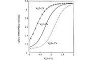
図11は、傾き調整電圧VnをパラメータとしたVCOの有効なノード静電容量Cと制御電圧Vcとの関係を示した特性図である。図11には、電圧Vcを制御することで、有効な静電容量感度を電気的に制御する様子を示している。この実施例では、レンジ調節電圧Vbを2Vにしている。また、傾き制御電圧Vnを、0.95V,1.1V,1.3Vに変更したデータを示している。図11において、制御電圧Vcを増加させるのに伴い、有効な静電容量Cは低下する。また、傾き調整電圧Vnを増加させるのに伴い、特性曲線は傾きが急峻となる。
【0080】
なお、図10及び図11に示したVCOでは、2つのキャパシタCの接続点には、キャパシタCc及びキャパシタCfの2つを接続した構成としたが、この構成に限るものではない。すなわち、さらに複数のキャパシタの一方の端子を2つのキャパシタCの接続点に接続し、該複数のキャパシタの他方の端子を電圧制御端子として制御電圧を印加することで、静電容量の値を大きくすることが可能となる。
【0081】
また、以上の説明では、Nウエルに不純物領域としてN+領域が形成されたMOSキャパシタについて説明したが、本発明はこの構成に限るものではない。すなわち、MOSキャパシタとして使用できるのであれば、ウエルはNウエルでもPウエルでも良く、ウエルに形成する不純物領域は、N+領域でもP+領域でも良い。
【0082】
【発明の効果】
本発明によれば、以下の効果が得られる。
【0083】
(1)マルチ端子型MOSバラクタでは、MOSキャパシタの浮遊電極に複数のキャパシタの一方の端子が接続されて、複数のキャパシタにおける他方の端子からは、制御電圧を印加可能である。したがって、複数のキャパシタにおける他方の端子から制御電圧を印加して、バイアス端子からバイアス電圧を印加することで、静電容量を連続的に変化させることができるとともに、製造時に発生したばらつきを調整することができる。また、プロセスステップを追加することなく、標準的なCMOSプロセスで作成することができる。
【0084】
(2)マルチ端子型MOSバラクタでは、j番目のキャパシタの前記他方の端子における有効な静電容量Cは、MOSキャパシタの浮遊電極に接続するキャパシタの個数によって変えることができる。
【0085】
(3)マルチ端子型MOSバラクタでは、同一シリコン基板における電気的に分離された複数のウエル上にMOSキャパシタ及びMOSキャパシタと同様の構成である複数のキャパシタが形成されている。そのため、プロセスステップを追加することなく、標準的なCMOSプロセスで作成することができ、製造コストを低減できる。
【図面の簡単な説明】
【図1】マルチ端子型MOSバラクタの概略構成図である。
【図2】図1に示したマルチ端子型MOSバラクタのバイアス電圧Vg1と有効な静電容量Cとの関係を示した特性図である。
【図3】図1に示したマルチ端子型MOSバラクタのC−V特性の実測曲線図である。
【図4】複数のキャパシタを備えたマルチ端子型MOSバラクタの構成図である。
【図5】シングル・ポリシリコン・CMOSプロセスによるマルチ端子型MOSバラクタの概略構成図である。
【図6】図5に示したシングル・ポリシリコン・CMOSプロセスによるマルチ端子型MOSバラクタの構成を変形した概略構成図である。
【図7】マルチ端子型バラクタを適用したLC型VCOの回路図である。
【図8】図7中の回路における静電容量Cと電圧Vcとの関係を示した特性図である。
【図9】マルチ端子型バラクタが適用され、C−Vc特性曲線の傾きを調節することが可能なVCOの回路図である。
【図10】レンジ調整電圧VbをパラメータとしたVCOの有効なノード静電容量Cと制御電圧Vcとの関係を示した特性図である。
【図11】傾き調整電圧VnをパラメータとしたVCOの有効なノード静電容量Cと制御電圧Vcとの関係を示した特性図である。
【図12】発振周波数を制御するためにMOSバラクタを用いた電圧制御発振器(VCO)の回路図及びバラクタの概略の構成図である。
【図13】従来の半導体可変容量素子の回路構成図である。
【符号の説明】
1,12:マルチ端子型MOSバラクタ
5:MOSキャパシタ(Cf)
6−1〜6−n:キャパシタ(C1〜Cn)
8:浮遊電極
9−1〜9−n:キャパシタ6−1〜6−nの他方の端子(Vg1〜Vgn)
11:MOSキャパシタ(Cf)5のウエル側の端子(Vn)[0001]
BACKGROUND OF THE INVENTION
The present invention is applicable to an integrated circuit, particularly a high-frequency integrated circuit, and relates to a MOS varactor that controls capacitance by voltages applied from a plurality of terminals.
[0002]
[Prior art]
The voltage controlled variable capacitor is a capacitor capable of controlling the electrostatic capacity according to the magnitude of the applied voltage, and is also referred to as a varactor. The varactor is manufactured by a CMOS process and uses (1) voltage-dependent characteristics of a PN junction diode or (2) voltage-dependent characteristics of a MOS capacitor. In particular, those corresponding to (2) are referred to as MOS varactors.
[0003]
Varactors are widely used in control circuits and oscillators. For example, a radio frequency oscillator (hereinafter referred to as an RF oscillator) uses a varactor to adjust the oscillation frequency to a specific value. In an LC (inductor-capacitor) oscillator which is a kind of RF oscillator, the oscillation frequency is generally determined by the relationship of the following equation.
[0004]
[Expression 2]
Therefore, in an LC oscillator using a varactor, the frequency can be adjusted by changing the capacitance value C. It is desirable that the characteristics of the varactor be controllable so that the capacity can be changed over a wide range. In addition, it is desirable to suppress the generation of capacitive components that affect the operation of the oscillator. By using a varactor having such characteristics, the control circuit and the oscillator can control the frequency over a wide range.
[0006]
Next, a conventional example using a varactor will be described. For example, in a voltage controlled oscillator (VCO), a MOS varactor is used as in the configuration shown in FIG. FIG. 12 is a circuit diagram of a voltage controlled oscillator (VCO) using a MOS varactor to control the oscillation frequency and a schematic configuration diagram of the varactor. This example is described in [AAAbidi, GJPottie, WJKaiser, “Power-Conscious Design Of Wireless Circuits And Systems.” Proceedings of the IEEE, vol. 88, (No. 10), pp. 1528-1545, October 2000]. This is a typical example of a voltage controlled oscillator (VCO) using a bank-structured MOS varactor. In this configuration, the effective electrostatic capacity can be changed by changing the tuning voltage (N-well bias voltage) by the MOS varactor. In addition, the MOS varactor has a plurality of capacitor banks that can store arbitrary binary values by switching the transistors on and off with control signals b0, b1, and b2, and discretely changes the VCO frequency. can do.
[0007]
FIG. 13 is a circuit configuration diagram of a semiconductor variable capacitance element disclosed in Japanese Patent Laid-Open No. 62-179162. In the present invention, since the electrostatic capacitance viewed from the capacitance terminal 105 can be adjusted by providing the bias terminal 103 capable of applying a bias voltage to the capacitance electrode 112 from the outside, the capacitance value can be changed by the bias voltage. Become. Further, the voltage of the external circuit to be connected can be cut by the bias cut capacitor 104, and a constant low bias voltage can be applied to the capacitor electrode 112. As a result, it is possible to prevent an unnecessary bias voltage from being applied to the capacitor electrode 112, and to realize a highly reliable semiconductor variable capacitor element in which the capacitance value does not change with time.
[0008]
13 is connected as the output terminal LO in FIG. 12, the semiconductor variable capacitance element circuit shown in FIG. 13 can be replaced with the MOS varactor of the VCO in FIG.
[0009]
[Problems to be solved by the invention]
The conventional MOS varactor can be easily implemented by a normal process of a CMOS integrated circuit without adding a new process step. In addition, the MOS varactor has a characteristic that a capacitance adjustment range is wide as compared with a diode (PN junction diode).
[0010]
However, the MOS varactor is a device having two terminals: (1) a gate and (2) a silicon well. That is, because of such a configuration, it is difficult to compensate for variations in electrical parameters generated in the process.
[0011]
Further, as described above, the circuit in FIG. 12 uses a plurality of capacitor banks that can store arbitrary binary values. However, since the frequency of the VCO is changed discretely by the capacitor bank as described above, there is a problem that the frequency of the VCO cannot be changed continuously. In addition, due to the switching transistors controlled by the control signals b0, b1 and b2, a large series resistance is added which reduces the VCO's figure of merit (Q factor). In order to compensate for the decrease in the Q factor, a very large rectifying transistor is required, but there is a problem that the occupied area increases.
[0012]
On the other hand, in the conventional example shown in FIG. 13 (Japanese Patent Laid-Open No. 62-179162), a bias terminal 103 is provided as a bias control terminal. When the bias point is adjusted or selected, it moves along the C-Vc curve. However, when the semiconductor variable capacitor of FIG. 13 is used for a VCO in a PLL (Phase Locked Loop) that is a closed loop, there is a problem that the sensitivity ΔC / ΔVc that affects the operation also changes. .
[0013]
As described above, in the conventional method using a PN junction diode or a MOS varactor, the control of the variable range of the capacitance is limited, and the sensitivity ΔC / ΔVc expressed by the ratio between the capacitance and the voltage is controlled. There is a problem that can not be.
[0014]
Therefore, the present invention has been made to solve the above problems, and an object of the present invention is to provide a MOS varactor capable of continuously changing the capacitance and controlling the frequency and sensitivity when applied to an oscillator. There is.
[0015]
[Means for Solving the Problems]
The present invention has the following configuration as means for solving the above problems.
[0016]
(1) formed in the wellImpurity region of the same conductivity type as the well Connected to the impurity regionbias A MOS capacitor having a terminal and a floating electrode facing the well; and a plurality of capacitors having one terminal connected to the floating electrode and capable of applying a control voltage from the other terminal. To do.
[0017]
In this configuration, in the multi-terminal MOS varactor, one terminal of a plurality of capacitors is connected to the floating electrode of the MOS capacitor. A control voltage can be applied from the other terminal of the plurality of capacitors. Therefore, by applying a control voltage from the other terminal of the plurality of capacitors,bias By applying a bias voltage from the terminal, it is possible to continuously change the capacitance, and it is possible to adjust a variation that occurs during manufacturing. Furthermore, it can be produced by a standard CMOS process without adding process steps.
[0018]
(2) Effective capacitance at the other terminal of the jth capacitor, where N is the number of the plurality of capacitors, and CM (Vf) is the capacitance of the MOS capacitor to which the potential Vf of the floating electrode is applied. Capacity
[0019]
[Equation 3]
It is characterized by being.
[0021]
In this configuration, in the multi-terminal MOS varactor, the effective capacitance C at the other terminal of the jth capacitor is
[0022]
[Expression 4]
It becomes. Accordingly, the effective capacitance C can be changed depending on the number of capacitors connected to the floating electrode of the MOS capacitor.
[0024]
(3) The plurality of capacitors are the MOS capacitorsSimilar to ConstitutionAnd The MOS capacitor and the plurality of capacitors are formed on a plurality of electrically isolated wells in the same silicon substrate.
[0025]
In this configuration, in the multi-terminal MOS varactor, a MOS capacitor and a MOS capacitor are formed on a plurality of wells that are electrically separated on the same silicon substrate.Similar to ConstitutionIs A plurality of capacitors are formed. Therefore, it is possible to create a standard CMOS process without adding process steps, and the manufacturing cost can be reduced.
[0030]
DETAILED DESCRIPTION OF THE INVENTION
FIG. 1 is a schematic configuration diagram of a multi-terminal MOS varactor. FIG. 1 shows a three-terminal MOS varactor as a basic configuration of a multi-terminal varactor. In short, the multi-terminal MOS varactor of the present invention has a configuration in which a control terminal is added to the MOS varactor. That is, the
[0031]
The MOS capacitor (Cf) 5 is provided between the N well 2 and the gate, and the gate which is one terminal is provided to face the well and serves as the floating electrode (Vf) 8. . The other terminal is connected to a bias terminal (Vn) 11 through an N +
[0032]
One terminal of the capacitor (C1) 6 and the capacitor (C2) 7 is connected to the floating electrode (Vf) 8. The other terminal of the capacitor (C1) 6 is connected to the control terminal (Vg1) 9, and the other terminal of the capacitor (C2) 7 is connected to the control terminal (Vg2) 10.
[0033]
The capacitor (C1) 6 and the capacitor (C2) 7 are constituted by MOS capacitors such as a double polysilicon capacitor (hereinafter referred to as DPC) and a metal insulator metal (hereinafter referred to as MIM) capacitor. good.
[0034]
The multi-terminal varactor according to the embodiment of the present invention can be implemented by a semiconductor process. The multi-terminal varactor is not limited to a high-frequency circuit up to 2 GHz, and can be applied to a general circuit. In addition, the multi-terminal varactor controls the voltage in order to correct the variation in parameters generated in the process or to continuously change the capacitance value in a wide range in the circuit applied to the VCO. The capacitance is adjusted.
[0035]
In the
[0036]
In the configuration of FIG. 1, the capacitance of the MOS capacitor (Cf) 5 changes according to the gate voltage (voltage of the floating electrode (Vf) 8) Vf. That is, the MOS capacitor (Cf) 5 whose capacitance is determined by the potential difference between the gate and the well is a MOS varactor (variable capacitor), and the effective capacitance is expressed by the following equation.
[0037]
[Equation 5]
In the above equation, the capacitance of the MOS capacitor (Cf) 5 is Cf, the capacitance of the capacitor (C1) 6 is C1, and the capacitance of the capacitor (C2) 7 is C2. Further, the voltage applied to the control terminal (Vg1) 9 is Vg1, the voltage applied to the control terminal (Vg2) 10 is Vg2, and the voltage applied to the bias terminal (Vn) 11 is Vn.
[0039]
FIG. 2 shows the relationship between the bias voltage Vg1 of the control terminal (Vg1) 9 and the effective capacitance C using the voltage value Vg2 applied to the terminal (Vg2) 10 in the
[0040]
[Formula 6]
It becomes.
[0042]
As described above, in the
[0043]
The voltage Vf at the floating electrode 8 (floating node) of the MOS capacitor (Cf) 5 is
[0044]
[Expression 7]
It becomes. Since the capacitance Cf of the MOS capacitor (Cf) is a function of the difference between the voltage Vf and the voltage Vn,
[0046]
[Equation 8]
It becomes.
[0048]
FIG. 3 is an actual measurement curve diagram of the CV characteristics of the MOS varactor implemented in the N well 2 shown as the MOS capacitor (Cf) 5 in FIG. As shown in FIG. 3, the effective capacitance C increases continuously as the value of (Vf−Vn) increases.
[0049]
Here, when the value of the effective capacitance C in the
[0050]
As shown in FIG. 4, the
[0051]
In this case, the effective capacitance at the control terminal (Vgj) 9-j of the jth capacitor is
[0052]
[Equation 9]
It is. Note that CM (Vf) is the capacitance of the MOS capacitor to which the potential Vf of the floating electrode is applied. The potential Vf of the floating electrode is applied from the control terminal (Vg1) 9-1 to the control terminal (Vgn) 9-n.Power N + 1 capacitors [n capacitors (C1) 6-1 to capacitors (Cn) 6-n and capacitors (Cf) 5) according to the voltage and the bias voltage applied from the N + 1 terminal of the bias terminal (Vn) 11 ] Determined by the capacitance.
[0054]
Next, an embodiment of a multi-terminal MOS varactor using a single polysilicon CMOS process will be described. FIG. 5 is a schematic configuration diagram of a multi-terminal MOS varactor using a single polysilicon CMOS process. The
[0055]
The MOS capacitor (Cf) 25 is provided between the N well 22 and the gate, and the gate which is one terminal is the floating electrode (Vf) 28. The other terminal is connected to a bias terminal (Vn) 31 through an N +
[0056]
The capacitor (C 1) 26 is provided between the N well 32 and the gate, and the gate which is one terminal is connected to the control terminal (Vg 1) 29. The other terminal is connected to the floating electrode (Vf) 28 via an N +
[0057]
The capacitor (C2) 27 is provided between the N well 35 and the gate, and the gate which is one terminal is connected to the floating electrode (Vf) 28. The other terminal is connected to the control terminal (Vg 2) 30 through an N +
[0058]
In the
[0059]
FIG. 6 is a schematic configuration diagram obtained by modifying the configuration of the multi-terminal MOS varactor by the single polysilicon / CMOS process shown in FIG. The
[0060]
The MOS capacitor (Cf) 45 is provided between the N well 42 and the gate, and the gate as one terminal is connected to the floating electrode (Vf) 48. The other terminal is connected to a bias terminal (Vn) 51 via an N +
[0061]
The capacitor (C 1) 46 is provided between the N well 52 and the gate, and the gate which is one terminal is connected to the control terminal (Vg 1) 49. The other terminal is connected to the floating electrode (Vf) 48 through an N +
[0062]
Capacitor (C2 47) is provided between the N well 55 and the gate, and the gate which is one terminal is connected to the control terminal (Vg2) 50. The other terminal is connected to the floating electrode (Vf) 48 through an N +
[0063]
Note that, in the
[0064]
As described above, the
[0065]
NextAnd ma A multi-terminal MOS varactor was applied to the VCO.Example Will be described. In the RF VCO, the controllability and tuning of the oscillation frequency are important as well as the reduction of the phase noise, and the multi-terminal varactor capable of realizing these can be applied to the LC VCO. FIG. 7 is a circuit diagram of an LC VCO to which a multi-terminal varactor is applied. The
[0066]
A
[0067]
The capacitor (Cc) 65 and the capacitor (Cf) 68 are low parasitic capacitance MIM capacitors (or DPCs), and a control voltage Vc is applied to the capacitor (Cc) 65. The MOS capacitor (C) 66 and the MOS capacitor (C) 67 are variable capacitors and are implemented using MOS capacitors (MOS varactors).
[0068]
Further, since the outputs V1 and V2 of the
[0069]
[Expression 10]
This value does not depend on the RF voltage (output voltage). Further, since there is a difference in the RF signal, the effective capacitance of the portion (C network) where each capacitor is connected as viewed from the output is not related to the capacitor (Cc) 65 and the capacitor (Cf) 68 of the RF oscillator. , Simply C.
[0071]
FIG. 8 is a characteristic diagram showing the relationship between the capacitance C and the voltage Vc in the circuit of FIG. FIG. 8 shows the relationship between the effective node capacitance C of the VCO and the control voltage Vc using the voltage Vn as a parameter. When the control voltage Vn is changed, the C-Vc curve shifts in the horizontal direction. thisExample Then, a bias voltage Vx = 1 V is applied to the
[0072]
FIG. 9 is a circuit diagram of a VCO to which a multi-terminal varactor is applied and the slope of the C-Vc characteristic curve can be adjusted. FIG. 10 is a characteristic diagram showing the relationship between the effective node capacitance C of the VCO and the control voltage Vc using the range adjustment voltage Vb as a parameter. The same parts as those in FIG. 9 are denoted by the same reference numerals, and detailed description thereof is omitted.
[0073]
The
[0074]
Capacitance C, Cc and Cf, lineTo The pressures Vc and Vn are used to adjust the operating point on the CV curve, ie the sensitivity ΔC / ΔVc. In a VCO using a multi-terminal varactor,
[0075]
[Expression 11]
It becomes.
[0077]
The capacitance Cb and the control voltage Vb are used to increase or decrease the absolute value of the capacitance C. This is shown in FIG. That is, the effective electrostatic capacity C decreases as the electrostatic capacity Cb increases. Further, the effective capacitance C decreases as the control voltage Vb is increased.
[0078]
In this circuit, a bias voltage Vx = 1 V is applied to the
[0079]
FIG. 11 is a characteristic diagram showing the relationship between the effective node capacitance C of the VCO and the control voltage Vc using the slope adjustment voltage Vn as a parameter. FIG. 11 shows a state in which the effective capacitance sensitivity is electrically controlled by controlling the voltage Vc. In this embodiment, the range adjustment voltage Vb is 2V. Further, data in which the slope control voltage Vn is changed to 0.95V, 1.1V, and 1.3V are shown. In FIG. 11, the effective capacitance C decreases as the control voltage Vc is increased. In addition, as the slope adjustment voltage Vn is increased, the slope of the characteristic curve becomes steep.
[0080]
In the VCO shown in FIG. 10 and FIG. 11, two capacitors Cc and Cf are connected to the connection point of the two capacitors C.But this The configuration is not limited to the above. That is, by connecting one terminal of the plurality of capacitors to the connection point of the two capacitors C and applying the control voltage using the other terminal of the plurality of capacitors as the voltage control terminal, the capacitance value is increased. It becomes possible to do.
[0081]
In the above description, the MOS capacitor in which the N + region is formed as the impurity region in the N well has been described. However, the present invention is not limited to this configuration. That is, as long as it can be used as a MOS capacitor, the well may be an N well or a P well, and the impurity region formed in the well may be an N + region or a P + region.
[0082]
【The invention's effect】
According to the present invention, the following effects can be obtained.
[0083]
(1) In a multi-terminal MOS varactor, one terminal of a plurality of capacitors is connected to a floating electrode of a MOS capacitor, and a control voltage can be applied from the other terminal of the plurality of capacitors. Therefore, by applying a control voltage from the other terminal of the plurality of capacitors,bias By applying a bias voltage from the terminal, it is possible to continuously change the capacitance, and it is possible to adjust variations that occur during manufacturing. Further, it can be formed by a standard CMOS process without adding process steps.
[0084]
(2) In the multi-terminal MOS varactor, the effective capacitance C at the other terminal of the jth capacitor can be changed according to the number of capacitors connected to the floating electrode of the MOS capacitor.
[0085]
(3) In a multi-terminal MOS varactor, a MOS capacitor and a MOS capacitor are provided on a plurality of wells that are electrically isolated on the same silicon substrate.Similar to ConstitutionIs A plurality of capacitors are formed. Therefore, a standard CMOS process can be used without adding process steps, and the manufacturing cost can be reduced.
[Brief description of the drawings]
FIG. 1 is a schematic configuration diagram of a multi-terminal MOS varactor.
FIG. 2 is a characteristic diagram showing a relationship between a bias voltage Vg1 and an effective capacitance C of the multi-terminal MOS varactor shown in FIG.
3 is an actual measurement curve diagram of CV characteristics of the multi-terminal MOS varactor shown in FIG. 1; FIG.
FIG. 4 is a configuration diagram of a multi-terminal MOS varactor including a plurality of capacitors.
FIG. 5 is a schematic configuration diagram of a multi-terminal MOS varactor based on a single polysilicon CMOS process.
6 is a schematic configuration diagram showing a modification of the configuration of the multi-terminal MOS varactor using the single polysilicon CMOS process shown in FIG. 5;
FIG. 7 is a circuit diagram of an LC VCO to which a multi-terminal varactor is applied.
8 is a characteristic diagram showing the relationship between the capacitance C and the voltage Vc in the circuit in FIG.
FIG. 9 is a circuit diagram of a VCO to which a multi-terminal varactor is applied and the slope of a C-Vc characteristic curve can be adjusted.
FIG. 10 is a characteristic diagram showing the relationship between the effective node capacitance C of the VCO and the control voltage Vc using the range adjustment voltage Vb as a parameter.
FIG. 11 is a characteristic diagram showing the relationship between the effective node capacitance C of the VCO and the control voltage Vc using the slope adjustment voltage Vn as a parameter.
FIG. 12 is a circuit diagram of a voltage controlled oscillator (VCO) using a MOS varactor to control the oscillation frequency, and a schematic configuration diagram of the varactor.
FIG. 13 is a circuit configuration diagram of a conventional semiconductor variable capacitance element.
[Explanation of symbols]
1,12: Multi-terminal MOS varactor
5: MOS capacitor (Cf)
6-1 to 6-n: capacitors (C1 to Cn)
8: Floating electrode
9-1 to 9-n: other terminals (Vg1 to Vgn) of the capacitors 6-1 to 6-n
11: terminal (Vn) on the well side of the MOS capacitor (Cf) 5
Claims (3)
Translated fromJapanesePriority Applications (6)
| Application Number | Priority Date | Filing Date | Title |
|---|---|---|---|
| JP2002011757AJP3877597B2 (en) | 2002-01-21 | 2002-01-21 | Multi-terminal MOS varactor |
| US10/345,404US6798011B2 (en) | 2002-01-21 | 2003-01-16 | Multi-terminal MOS varactor |
| KR10-2003-0003617AKR100491280B1 (en) | 2002-01-21 | 2003-01-20 | Multi-terminal mos varactor |
| TW092101235ATWI223445B (en) | 2002-01-21 | 2003-01-21 | Multi-terminal MOS varactor |
| EP03250374AEP1333501A3 (en) | 2002-01-21 | 2003-01-21 | Multi-terminal MOS varactor |
| CNB03102792XACN1221036C (en) | 2002-01-21 | 2003-01-21 | Multi-terminal MOS varactor |
Applications Claiming Priority (1)
| Application Number | Priority Date | Filing Date | Title |
|---|---|---|---|
| JP2002011757AJP3877597B2 (en) | 2002-01-21 | 2002-01-21 | Multi-terminal MOS varactor |
Publications (2)
| Publication Number | Publication Date |
|---|---|
| JP2003218217A JP2003218217A (en) | 2003-07-31 |
| JP3877597B2true JP3877597B2 (en) | 2007-02-07 |
Family
ID=19191700
Family Applications (1)
| Application Number | Title | Priority Date | Filing Date |
|---|---|---|---|
| JP2002011757AExpired - Fee RelatedJP3877597B2 (en) | 2002-01-21 | 2002-01-21 | Multi-terminal MOS varactor |
Country Status (6)
| Country | Link |
|---|---|
| US (1) | US6798011B2 (en) |
| EP (1) | EP1333501A3 (en) |
| JP (1) | JP3877597B2 (en) |
| KR (1) | KR100491280B1 (en) |
| CN (1) | CN1221036C (en) |
| TW (1) | TWI223445B (en) |
Families Citing this family (36)
| Publication number | Priority date | Publication date | Assignee | Title |
|---|---|---|---|---|
| US6847095B2 (en)* | 2003-04-01 | 2005-01-25 | Texas Instruments Incorporated | Variable reactor (varactor) with engineered capacitance-voltage characteristics |
| CN100508387C (en)* | 2003-11-21 | 2009-07-01 | 瑞昱半导体股份有限公司 | phase delay circuit |
| US7223667B2 (en)* | 2004-04-21 | 2007-05-29 | Taiwan Semiconductor Manufacturing Company, Ltd. | Compensated linearity voltage-control-capacitor device by standard CMOS process |
| US7068089B2 (en)* | 2004-05-28 | 2006-06-27 | Wionics Research | Digitally programmable I/Q phase offset compensation |
| US7922065B2 (en)* | 2004-08-02 | 2011-04-12 | Ati Properties, Inc. | Corrosion resistant fluid conducting parts, methods of making corrosion resistant fluid conducting parts and equipment and parts replacement methods utilizing corrosion resistant fluid conducting parts |
| US7714412B2 (en)* | 2004-08-27 | 2010-05-11 | International Business Machines Corporation | MOS varactor using isolation well |
| US7612397B2 (en)* | 2006-11-10 | 2009-11-03 | Sharp Kabushiki Kaisha | Memory cell having first and second capacitors with electrodes acting as control gates for nonvolatile memory transistors |
| US20080149983A1 (en)* | 2006-12-20 | 2008-06-26 | International Business Machines Corporation | Metal-oxide-semiconductor (mos) varactors and methods of forming mos varactors |
| US8130051B2 (en)* | 2008-02-06 | 2012-03-06 | Broadcom Corporation | Method and system for varactor linearization |
| CN102446985B (en)* | 2010-10-14 | 2013-11-27 | 众智光电科技股份有限公司 | Hybrid stack structure consisting of photodiodes and capacitive submounts |
| JP5569689B2 (en) | 2010-10-15 | 2014-08-13 | ソニー株式会社 | Variable capacity device, antenna module, and communication device |
| US8692608B2 (en) | 2011-09-19 | 2014-04-08 | United Microelectronics Corp. | Charge pump system capable of stabilizing an output voltage |
| US9030221B2 (en) | 2011-09-20 | 2015-05-12 | United Microelectronics Corporation | Circuit structure of test-key and test method thereof |
| US8395455B1 (en) | 2011-10-14 | 2013-03-12 | United Microelectronics Corp. | Ring oscillator |
| US8421509B1 (en) | 2011-10-25 | 2013-04-16 | United Microelectronics Corp. | Charge pump circuit with low clock feed-through |
| US8588020B2 (en) | 2011-11-16 | 2013-11-19 | United Microelectronics Corporation | Sense amplifier and method for determining values of voltages on bit-line pair |
| US8493806B1 (en) | 2012-01-03 | 2013-07-23 | United Microelectronics Corporation | Sense-amplifier circuit of memory and calibrating method thereof |
| US8970197B2 (en) | 2012-08-03 | 2015-03-03 | United Microelectronics Corporation | Voltage regulating circuit configured to have output voltage thereof modulated digitally |
| US8724404B2 (en) | 2012-10-15 | 2014-05-13 | United Microelectronics Corp. | Memory, supply voltage generation circuit, and operation method of a supply voltage generation circuit used for a memory array |
| US8669897B1 (en) | 2012-11-05 | 2014-03-11 | United Microelectronics Corp. | Asynchronous successive approximation register analog-to-digital converter and operating method thereof |
| US8711598B1 (en) | 2012-11-21 | 2014-04-29 | United Microelectronics Corp. | Memory cell and memory cell array using the same |
| US8873295B2 (en) | 2012-11-27 | 2014-10-28 | United Microelectronics Corporation | Memory and operation method thereof |
| US8643521B1 (en) | 2012-11-28 | 2014-02-04 | United Microelectronics Corp. | Digital-to-analog converter with greater output resistance |
| US9030886B2 (en) | 2012-12-07 | 2015-05-12 | United Microelectronics Corp. | Memory device and driving method thereof |
| US8953401B2 (en) | 2012-12-07 | 2015-02-10 | United Microelectronics Corp. | Memory device and method for driving memory array thereof |
| US9299699B2 (en) | 2013-03-13 | 2016-03-29 | Taiwan Semiconductor Manufacturing Company, Ltd. | Multi-gate and complementary varactors in FinFET process |
| US8917109B2 (en) | 2013-04-03 | 2014-12-23 | United Microelectronics Corporation | Method and device for pulse width estimation |
| US9105355B2 (en) | 2013-07-04 | 2015-08-11 | United Microelectronics Corporation | Memory cell array operated with multiple operation voltage |
| US10491209B2 (en)* | 2013-07-17 | 2019-11-26 | Qualcomm Incorporated | Switch linearizer |
| US8947911B1 (en) | 2013-11-07 | 2015-02-03 | United Microelectronics Corp. | Method and circuit for optimizing bit line power consumption |
| US8866536B1 (en) | 2013-11-14 | 2014-10-21 | United Microelectronics Corp. | Process monitoring circuit and method |
| US9143143B2 (en) | 2014-01-13 | 2015-09-22 | United Microelectronics Corp. | VCO restart up circuit and method thereof |
| US9837555B2 (en) | 2015-04-15 | 2017-12-05 | Futurewei Technologies, Inc. | Apparatus and method for a low loss coupling capacitor |
| US10367450B2 (en)* | 2015-12-15 | 2019-07-30 | Mediatek Inc. | Oscillator scheme capable of reducing far-out phase noise and closed-in phase noise |
| US10461696B2 (en) | 2017-10-23 | 2019-10-29 | Analog Devices, Inc. | Switched capacitor banks |
| US10469029B2 (en) | 2017-10-23 | 2019-11-05 | Analog Devices, Inc. | Inductor current distribution |
Family Cites Families (5)
| Publication number | Priority date | Publication date | Assignee | Title |
|---|---|---|---|---|
| JPS62179162A (en) | 1986-01-31 | 1987-08-06 | Seiko Instr & Electronics Ltd | semiconductor variable capacitance element |
| JP2662559B2 (en)* | 1989-06-02 | 1997-10-15 | 直 柴田 | Semiconductor device |
| US6268777B1 (en)* | 1997-11-20 | 2001-07-31 | Applied Micro Circuits Corporation | Single inductor fully integrated differential voltage controlled oscillator with automatic amplitude adjustment and on-chip varactor |
| US6667506B1 (en)* | 1999-04-06 | 2003-12-23 | Peregrine Semiconductor Corporation | Variable capacitor with programmability |
| US6621128B2 (en)* | 2001-02-28 | 2003-09-16 | United Microelectronics Corp. | Method of fabricating a MOS capacitor |
- 2002
- 2002-01-21JPJP2002011757Apatent/JP3877597B2/ennot_activeExpired - Fee Related
- 2003
- 2003-01-16USUS10/345,404patent/US6798011B2/ennot_activeExpired - Fee Related
- 2003-01-20KRKR10-2003-0003617Apatent/KR100491280B1/ennot_activeExpired - Fee Related
- 2003-01-21EPEP03250374Apatent/EP1333501A3/ennot_activeWithdrawn
- 2003-01-21CNCNB03102792XApatent/CN1221036C/ennot_activeExpired - Fee Related
- 2003-01-21TWTW092101235Apatent/TWI223445B/ennot_activeIP Right Cessation
Also Published As
| Publication number | Publication date |
|---|---|
| TW200308087A (en) | 2003-12-16 |
| KR100491280B1 (en) | 2005-05-24 |
| CN1221036C (en) | 2005-09-28 |
| CN1434519A (en) | 2003-08-06 |
| EP1333501A2 (en) | 2003-08-06 |
| JP2003218217A (en) | 2003-07-31 |
| TWI223445B (en) | 2004-11-01 |
| EP1333501A3 (en) | 2005-01-05 |
| US20030136992A1 (en) | 2003-07-24 |
| KR20030063202A (en) | 2003-07-28 |
| US6798011B2 (en) | 2004-09-28 |
Similar Documents
| Publication | Publication Date | Title |
|---|---|---|
| JP3877597B2 (en) | Multi-terminal MOS varactor | |
| US6509805B2 (en) | LC resonance circuit and voltage-controlled oscillation circuit | |
| US8134414B2 (en) | Clock, frequency reference, and other reference signal generator with frequency stability over temperature variation | |
| US7564318B2 (en) | Switch capacitance and varactor banks applied to voltage controlled oscillator having constant frequency tuning sensitivity | |
| US20080012654A1 (en) | Linearized variable-capacitance module and lc resonance circuit using the same | |
| EP2961062B1 (en) | Apparatus and methods for switch-coupled oscillators | |
| US7675374B2 (en) | Voltage controlled oscillator with switching bias | |
| US8098109B2 (en) | Differential varactor circuit for a voltage controlled oscillator | |
| US8222963B2 (en) | Voltage-controlled oscillator | |
| US7098751B1 (en) | Tunable capacitance circuit for voltage control oscillator | |
| US7569912B2 (en) | Differential variable capacitors and their applications | |
| US6320474B1 (en) | MOS-type capacitor and integrated circuit VCO using same | |
| US6720835B2 (en) | Voltage-controlled oscillation circuit | |
| US7034626B2 (en) | Oscillator with closed series of four inductors and four capacitors with connecting nodes | |
| WO2007072551A1 (en) | Voltage controlled ring oscillator | |
| US6566971B1 (en) | Method and circuitry for implementing a differentially tuned varactor-inductor oscillator | |
| JP2004056818A (en) | Oscillator, PLL circuit, communication device, oscillation method | |
| US20050206465A1 (en) | Voltage control oscillator | |
| JP4667924B2 (en) | Variable capacitance circuit and control method of variable capacitance circuit | |
| US20010035797A1 (en) | Method and circuitry for implementing a differentially tuned varactor-inductor oscillator | |
| JP2002190709A (en) | Voltage controlled oscillation circuit | |
| CN102959857B (en) | Circuit Configuration of a Voltage Controlled Oscillator | |
| JP2007074126A (en) | Variable capacitance element and voltage controlled oscillator |
Legal Events
| Date | Code | Title | Description |
|---|---|---|---|
| A621 | Written request for application examination | Free format text:JAPANESE INTERMEDIATE CODE: A621 Effective date:20040728 | |
| A977 | Report on retrieval | Free format text:JAPANESE INTERMEDIATE CODE: A971007 Effective date:20050915 | |
| A131 | Notification of reasons for refusal | Free format text:JAPANESE INTERMEDIATE CODE: A131 Effective date:20051004 | |
| A521 | Request for written amendment filed | Free format text:JAPANESE INTERMEDIATE CODE: A523 Effective date:20051205 | |
| TRDD | Decision of grant or rejection written | ||
| A01 | Written decision to grant a patent or to grant a registration (utility model) | Free format text:JAPANESE INTERMEDIATE CODE: A01 Effective date:20061003 | |
| A61 | First payment of annual fees (during grant procedure) | Free format text:JAPANESE INTERMEDIATE CODE: A61 Effective date:20061031 | |
| R150 | Certificate of patent or registration of utility model | Free format text:JAPANESE INTERMEDIATE CODE: R150 | |
| FPAY | Renewal fee payment (event date is renewal date of database) | Free format text:PAYMENT UNTIL: 20091110 Year of fee payment:3 | |
| FPAY | Renewal fee payment (event date is renewal date of database) | Free format text:PAYMENT UNTIL: 20101110 Year of fee payment:4 | |
| FPAY | Renewal fee payment (event date is renewal date of database) | Free format text:PAYMENT UNTIL: 20111110 Year of fee payment:5 | |
| FPAY | Renewal fee payment (event date is renewal date of database) | Free format text:PAYMENT UNTIL: 20111110 Year of fee payment:5 | |
| FPAY | Renewal fee payment (event date is renewal date of database) | Free format text:PAYMENT UNTIL: 20121110 Year of fee payment:6 | |
| FPAY | Renewal fee payment (event date is renewal date of database) | Free format text:PAYMENT UNTIL: 20121110 Year of fee payment:6 | |
| FPAY | Renewal fee payment (event date is renewal date of database) | Free format text:PAYMENT UNTIL: 20131110 Year of fee payment:7 | |
| LAPS | Cancellation because of no payment of annual fees |