JP3877302B2 - Method for forming carbon nanotube - Google Patents
Method for forming carbon nanotubeDownload PDFInfo
- Publication number
- JP3877302B2 JP3877302B2JP2002182468AJP2002182468AJP3877302B2JP 3877302 B2JP3877302 B2JP 3877302B2JP 2002182468 AJP2002182468 AJP 2002182468AJP 2002182468 AJP2002182468 AJP 2002182468AJP 3877302 B2JP3877302 B2JP 3877302B2
- Authority
- JP
- Japan
- Prior art keywords
- forming
- carbon nanotube
- metal
- alloy
- carbon nanotubes
- Prior art date
- Legal status (The legal status is an assumption and is not a legal conclusion. Google has not performed a legal analysis and makes no representation as to the accuracy of the status listed.)
- Expired - Fee Related
Links
Images


Classifications
- C—CHEMISTRY; METALLURGY
- C01—INORGANIC CHEMISTRY
- C01B—NON-METALLIC ELEMENTS; COMPOUNDS THEREOF; METALLOIDS OR COMPOUNDS THEREOF NOT COVERED BY SUBCLASS C01C
- C01B32/00—Carbon; Compounds thereof
- C01B32/15—Nano-sized carbon materials
- C01B32/158—Carbon nanotubes
- C01B32/16—Preparation
- C01B32/162—Preparation characterised by catalysts
- B—PERFORMING OPERATIONS; TRANSPORTING
- B01—PHYSICAL OR CHEMICAL PROCESSES OR APPARATUS IN GENERAL
- B01J—CHEMICAL OR PHYSICAL PROCESSES, e.g. CATALYSIS OR COLLOID CHEMISTRY; THEIR RELEVANT APPARATUS
- B01J23/00—Catalysts comprising metals or metal oxides or hydroxides, not provided for in group B01J21/00
- B01J23/16—Catalysts comprising metals or metal oxides or hydroxides, not provided for in group B01J21/00 of arsenic, antimony, bismuth, vanadium, niobium, tantalum, polonium, chromium, molybdenum, tungsten, manganese, technetium or rhenium
- B01J23/24—Chromium, molybdenum or tungsten
- B01J23/28—Molybdenum
- B—PERFORMING OPERATIONS; TRANSPORTING
- B01—PHYSICAL OR CHEMICAL PROCESSES OR APPARATUS IN GENERAL
- B01J—CHEMICAL OR PHYSICAL PROCESSES, e.g. CATALYSIS OR COLLOID CHEMISTRY; THEIR RELEVANT APPARATUS
- B01J23/00—Catalysts comprising metals or metal oxides or hydroxides, not provided for in group B01J21/00
- B01J23/70—Catalysts comprising metals or metal oxides or hydroxides, not provided for in group B01J21/00 of the iron group metals or copper
- B01J23/74—Iron group metals
- B01J23/745—Iron
- B—PERFORMING OPERATIONS; TRANSPORTING
- B01—PHYSICAL OR CHEMICAL PROCESSES OR APPARATUS IN GENERAL
- B01J—CHEMICAL OR PHYSICAL PROCESSES, e.g. CATALYSIS OR COLLOID CHEMISTRY; THEIR RELEVANT APPARATUS
- B01J23/00—Catalysts comprising metals or metal oxides or hydroxides, not provided for in group B01J21/00
- B01J23/70—Catalysts comprising metals or metal oxides or hydroxides, not provided for in group B01J21/00 of the iron group metals or copper
- B01J23/74—Iron group metals
- B01J23/75—Cobalt
- B—PERFORMING OPERATIONS; TRANSPORTING
- B01—PHYSICAL OR CHEMICAL PROCESSES OR APPARATUS IN GENERAL
- B01J—CHEMICAL OR PHYSICAL PROCESSES, e.g. CATALYSIS OR COLLOID CHEMISTRY; THEIR RELEVANT APPARATUS
- B01J23/00—Catalysts comprising metals or metal oxides or hydroxides, not provided for in group B01J21/00
- B01J23/70—Catalysts comprising metals or metal oxides or hydroxides, not provided for in group B01J21/00 of the iron group metals or copper
- B01J23/74—Iron group metals
- B01J23/755—Nickel
- B—PERFORMING OPERATIONS; TRANSPORTING
- B01—PHYSICAL OR CHEMICAL PROCESSES OR APPARATUS IN GENERAL
- B01J—CHEMICAL OR PHYSICAL PROCESSES, e.g. CATALYSIS OR COLLOID CHEMISTRY; THEIR RELEVANT APPARATUS
- B01J35/00—Catalysts, in general, characterised by their form or physical properties
- B01J35/40—Catalysts, in general, characterised by their form or physical properties characterised by dimensions, e.g. grain size
- B01J35/45—Nanoparticles
- B—PERFORMING OPERATIONS; TRANSPORTING
- B01—PHYSICAL OR CHEMICAL PROCESSES OR APPARATUS IN GENERAL
- B01J—CHEMICAL OR PHYSICAL PROCESSES, e.g. CATALYSIS OR COLLOID CHEMISTRY; THEIR RELEVANT APPARATUS
- B01J37/00—Processes, in general, for preparing catalysts; Processes, in general, for activation of catalysts
- B01J37/02—Impregnation, coating or precipitation
- B01J37/0238—Impregnation, coating or precipitation via the gaseous phase-sublimation
- B—PERFORMING OPERATIONS; TRANSPORTING
- B01—PHYSICAL OR CHEMICAL PROCESSES OR APPARATUS IN GENERAL
- B01J—CHEMICAL OR PHYSICAL PROCESSES, e.g. CATALYSIS OR COLLOID CHEMISTRY; THEIR RELEVANT APPARATUS
- B01J37/00—Processes, in general, for preparing catalysts; Processes, in general, for activation of catalysts
- B01J37/02—Impregnation, coating or precipitation
- B01J37/024—Multiple impregnation or coating
- B01J37/0244—Coatings comprising several layers
- B—PERFORMING OPERATIONS; TRANSPORTING
- B01—PHYSICAL OR CHEMICAL PROCESSES OR APPARATUS IN GENERAL
- B01J—CHEMICAL OR PHYSICAL PROCESSES, e.g. CATALYSIS OR COLLOID CHEMISTRY; THEIR RELEVANT APPARATUS
- B01J37/00—Processes, in general, for preparing catalysts; Processes, in general, for activation of catalysts
- B01J37/08—Heat treatment
- B—PERFORMING OPERATIONS; TRANSPORTING
- B82—NANOTECHNOLOGY
- B82Y—SPECIFIC USES OR APPLICATIONS OF NANOSTRUCTURES; MEASUREMENT OR ANALYSIS OF NANOSTRUCTURES; MANUFACTURE OR TREATMENT OF NANOSTRUCTURES
- B82Y30/00—Nanotechnology for materials or surface science, e.g. nanocomposites
- B—PERFORMING OPERATIONS; TRANSPORTING
- B82—NANOTECHNOLOGY
- B82Y—SPECIFIC USES OR APPLICATIONS OF NANOSTRUCTURES; MEASUREMENT OR ANALYSIS OF NANOSTRUCTURES; MANUFACTURE OR TREATMENT OF NANOSTRUCTURES
- B82Y40/00—Manufacture or treatment of nanostructures
- H—ELECTRICITY
- H01—ELECTRIC ELEMENTS
- H01M—PROCESSES OR MEANS, e.g. BATTERIES, FOR THE DIRECT CONVERSION OF CHEMICAL ENERGY INTO ELECTRICAL ENERGY
- H01M8/00—Fuel cells; Manufacture thereof
- H01M8/02—Details
- H01M8/0202—Collectors; Separators, e.g. bipolar separators; Interconnectors
- H01M8/023—Porous and characterised by the material
- H01M8/0234—Carbonaceous material
- B—PERFORMING OPERATIONS; TRANSPORTING
- B01—PHYSICAL OR CHEMICAL PROCESSES OR APPARATUS IN GENERAL
- B01J—CHEMICAL OR PHYSICAL PROCESSES, e.g. CATALYSIS OR COLLOID CHEMISTRY; THEIR RELEVANT APPARATUS
- B01J23/00—Catalysts comprising metals or metal oxides or hydroxides, not provided for in group B01J21/00
- B01J23/38—Catalysts comprising metals or metal oxides or hydroxides, not provided for in group B01J21/00 of noble metals
- B01J23/54—Catalysts comprising metals or metal oxides or hydroxides, not provided for in group B01J21/00 of noble metals combined with metals, oxides or hydroxides provided for in groups B01J23/02 - B01J23/36
- B01J23/56—Platinum group metals
- C—CHEMISTRY; METALLURGY
- C01—INORGANIC CHEMISTRY
- C01B—NON-METALLIC ELEMENTS; COMPOUNDS THEREOF; METALLOIDS OR COMPOUNDS THEREOF NOT COVERED BY SUBCLASS C01C
- C01B2202/00—Structure or properties of carbon nanotubes
- C01B2202/06—Multi-walled nanotubes
- C—CHEMISTRY; METALLURGY
- C01—INORGANIC CHEMISTRY
- C01B—NON-METALLIC ELEMENTS; COMPOUNDS THEREOF; METALLOIDS OR COMPOUNDS THEREOF NOT COVERED BY SUBCLASS C01C
- C01B2202/00—Structure or properties of carbon nanotubes
- C01B2202/20—Nanotubes characterized by their properties
- C01B2202/36—Diameter
- Y—GENERAL TAGGING OF NEW TECHNOLOGICAL DEVELOPMENTS; GENERAL TAGGING OF CROSS-SECTIONAL TECHNOLOGIES SPANNING OVER SEVERAL SECTIONS OF THE IPC; TECHNICAL SUBJECTS COVERED BY FORMER USPC CROSS-REFERENCE ART COLLECTIONS [XRACs] AND DIGESTS
- Y02—TECHNOLOGIES OR APPLICATIONS FOR MITIGATION OR ADAPTATION AGAINST CLIMATE CHANGE
- Y02E—REDUCTION OF GREENHOUSE GAS [GHG] EMISSIONS, RELATED TO ENERGY GENERATION, TRANSMISSION OR DISTRIBUTION
- Y02E60/00—Enabling technologies; Technologies with a potential or indirect contribution to GHG emissions mitigation
- Y02E60/30—Hydrogen technology
- Y02E60/50—Fuel cells
- Y—GENERAL TAGGING OF NEW TECHNOLOGICAL DEVELOPMENTS; GENERAL TAGGING OF CROSS-SECTIONAL TECHNOLOGIES SPANNING OVER SEVERAL SECTIONS OF THE IPC; TECHNICAL SUBJECTS COVERED BY FORMER USPC CROSS-REFERENCE ART COLLECTIONS [XRACs] AND DIGESTS
- Y02—TECHNOLOGIES OR APPLICATIONS FOR MITIGATION OR ADAPTATION AGAINST CLIMATE CHANGE
- Y02P—CLIMATE CHANGE MITIGATION TECHNOLOGIES IN THE PRODUCTION OR PROCESSING OF GOODS
- Y02P70/00—Climate change mitigation technologies in the production process for final industrial or consumer products
- Y02P70/50—Manufacturing or production processes characterised by the final manufactured product
Landscapes
- Chemical & Material Sciences (AREA)
- Engineering & Computer Science (AREA)
- Materials Engineering (AREA)
- Organic Chemistry (AREA)
- Chemical Kinetics & Catalysis (AREA)
- Nanotechnology (AREA)
- Physics & Mathematics (AREA)
- Manufacturing & Machinery (AREA)
- General Physics & Mathematics (AREA)
- Crystallography & Structural Chemistry (AREA)
- Condensed Matter Physics & Semiconductors (AREA)
- Thermal Sciences (AREA)
- Inorganic Chemistry (AREA)
- Life Sciences & Earth Sciences (AREA)
- Sustainable Development (AREA)
- Sustainable Energy (AREA)
- Electrochemistry (AREA)
- General Chemical & Material Sciences (AREA)
- Composite Materials (AREA)
- Carbon And Carbon Compounds (AREA)
- Inert Electrodes (AREA)
- Catalysts (AREA)
Description
Translated fromJapanese【0001】
【発明の属する技術分野】
本発明は、小型の燃料電池(FC)等において用いられる炭素系薄膜の製造方法に関する。特に、導電性材料上にカーボンナノチューブ(CNT)を形成するための方法に関する。
【0002】
【従来の技術】
カーボンナノチューブは、炭素からなるナノメートルのオーダーの直径を有する円筒形のチューブであり、その優れた特性から様々な用途での応用が期待されている。例えば、特開2002−141084号公報には、燃料電池において、白金などの触媒を担持する担持体としてカーボンナノチューブからなる炭素膜を用いることが開示されている。カーボンナノチューブは多孔質であることからガス拡散層としても働く。この公報に開示された発明では、金などからなる電極端子膜上に形成された鉄またはニッケル膜の上にカーボンナノチューブ膜を形成し、その表面に白金触媒をスパッタリングにより被着させている。
【0003】
カーボンナノチューブを形成する方法としては、アーク放電を用いるものや加熱によるものがある。例えば、特開2001−58805には、カーボンナノチューブを大量かつ簡易に製造する方法として、フラーレン分子と遷移金属元素または遷移金属元素を含む合金とを混合し、セラミックのボード上で加熱することが開示されている。しかしながら、この刊行物には、カーボンナノチューブを導電性材料上に形成することについては記載がない。
【0004】
また、カーボンナノチューブの形成において鉄やニッケルなどの遷移金属を微粒子化したものを触媒として用いることが知られている。このような金属微粒子の形成方法としては、金属薄膜をレーザやマイクロ波などでエッチングする方法やゼオライトやポーラスシリコンなどの細孔に埋める方法などがある。
【0005】
【発明が解決しようとする課題】
本発明の主たる目的は、導電性材料上にカーボンナノチューブを形成するための、改善された方法を提供することである。
【0006】
本発明の第2の目的は、カーボンナノチューブを成長させる際に触媒として働く金属微粒子を簡易なプロセスで安価に且つ効率よく得ることが可能なカーボンナノチューブ形成方法を提供することである。
【0007】
本発明の第3の目的は、小型燃料電池で用いるのに適したカーボンナノチューブを形成するための方法を提供することである。
【0008】
【課題を解決するための手段】
前記目的を達成するため本発明に基づくと、導電性材料(2)上にカーボンナノチューブ(5)を形成する方法であって、カーボンナノチューブを成長させる際に触媒として働く金属または合金を含む触媒層(3)を導電性材料上に形成する過程と、触媒層の金属または合金を処理して微粒子化する過程と、金属または合金の微粒子(3a)を触媒として導電性材料上にカーボンナノチューブを形成する過程とを有し、触媒層の金属または合金を処理して微粒子化する過程が、不活性ガスを供給しつつ、導電性材料上に形成された触媒層を所定の温度で加熱する過程を有することを特徴とするカーボンナノチューブの形成方法が提供される。このようにすることにより、カーボンナノチューブを成長させる際に触媒として働く金属または合金微粒子を簡単なプロセスで容易に且つ安価に形成し、それらを触媒として用いることで、カーボンナノチューブを導電性材料上に効率的に形成することができる。
【0009】
触媒層は、好適には、Fe、Ni、CoまたはMoの何れか或いはその合金を含む。導電性材料は、Ti、Au、Ni、Co、Cu、Al、Mo、W、もしくはTaの少なくとも一つを含むものとすることができる。また、不活性ガスはヘリウムまたはアルゴンとするとよい。
【0010】
触媒層の金属または合金を微粒子化するときの所定の温度は、金属または合金の絶対温度で表した融点をTmとしたとき、0.49Tm〜0.59Tmの範囲にあるとよい。触媒層が鉄からなる場合、概ね700℃とするとよい。加熱温度が低すぎても高すぎても、粒子が粗大化して望ましい粒子サイズを得ることができない。また、金属または合金の微粒子は0.5〜50nmの粒子サイズを有すると好適である。そのような粒子サイズは、カーボンナノチューブ形成における触媒作用も十分に有し且つ上記方法によって容易に得ることができる。上記した加熱温度で触媒層の金属又は合金を微粒子化することにより、そのような粒子サイズを簡単なプロセスで効率よく形成することができる。
【0011】
カーボンナノチューブを形成する過程が、炭化水素ガス(原料ガス)と不活性ガスとを1:2乃至1:50の範囲で含む混合ガスを供給する過程を含むものとすると、カーボンナノチューブ以外のアモルファス炭素または煤の発生を抑制しつつ、カーボンナノチューブの成長速度が極度に遅くなるのを防いで効率よくカーボンナノチューブを生成することができるため好適である。
【0012】
供給する混合ガスの流速は、分速1〜100cmが好ましく、概ね分速30cmが特に好適である。それにより、煤の形成を抑制しつつ、カーボンナノチューブの形成に寄与することなく排出される原料ガスの量も低減し生産性を向上することができる。カーボンナノチューブを形成する過程が、概ね30mmの内径を有する管内に微粒子化された金属または合金を有する導電性材料を置いて行われる場合、管内に流す混合ガスの流量は概ね200乃至300sccmとするとよい。
【0013】
また、導電性材料は例えばシリコンやガラスのような無機質材基板上に付着されたものとすることができる。導電性材料を、例えばチタン(Ti)からなる層と、その上に形成された耐熱性に優れたタングステン(W)からなる層とからなる2層構造とすることもできる。チタンの代わりに、アルミニウム(Al)、ニッケル(Ni)、クロム(Cr)を代わりに用いることができる。また、タングステンの代わりにモリブデン(Mo)、タンタル(Ta)を用いることもできる。
【0014】
本発明の特徴、目的及び作用効果は、添付図面を参照しつつ好適実施例について説明することにより一層明らかとなるだろう。
【0015】
【発明の実施の形態】
以下、本発明の好適実施例について図面を参照して説明する。
【0016】
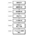
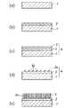
図1は、本発明に基づくカーボンナノチューブ形成方法の好適実施例を示すフロー図であり、図2は、図1のフロー図のいくつかのステップにおける状態を示す模式的な断面図である。
【0017】
ステップ1において、例えばシリコン(Si)やガラスからなる無機質基板1を清浄化する(図2(a))。
【0018】
続いてステップ2で、清浄化した無機質基板1上に例えばチタン(Ti)、金(Au)、ニッケル(Ni)、コバルト(Co)、銅(Cu)、アルミニウム(Al)、モリブデン(Mo)、タングステン(W)、タンタル(Ta)などの金属またはドープされた半導体のような導電性材料からなる導電層2を例えば抵抗加熱蒸着やスパッタリングなどにより形成する(図2(b))。無機質基板1がシリコンからなる場合、導電層2を基板上に形成されたチタン(Ti)層とその上に形成されたタングステン(W)層からなる二層構造とすると、タングステンの融点が高く、後の熱処理において影響を受けにくいため好適である。チタンはシリコンとの密着性改善の働きをし、アルミニウム(Al)、ニッケル(Ni)、クロム(Cr)を代わりに用いることができる。また、タングステンの代わりにモリブデン(Mo)、タンタル(Ta)を用いることもできる。無機質基板1が導電性を有するシリコン(例えばドープされたシリコン)からなる場合、外部との電気的接続に用いることができるため好都合なことがある。
【0019】
ステップ3では、カーボンナノチューブ膜成長のための触媒として働く、例えば鉄(Fe)のような遷移金属からなる触媒層3を導電層2上に形成する(図2(c))。これは例えば電子ビーム蒸着により行うことができる。鉄のかわりにニッケル(Ni)、コバルト(Co)、モリブデン(Mo)を用いることもできる。鉄、ニッケル、コバルト、モリブデンのうち2以上を混合して用いてもよい。あるいは、それらの合金を利用することもできる。尚、このように基板1上に導電層2及び触媒層3を形成したものを基体4と呼ぶ。
【0020】
ここで図3を参照すると、ステップ3において得られた基体4を処理して導電層2上にカーボンナノチューブを形成するための好適な製造装置を表す模式的な縦断面図が示されている。この装置10は、例えば内径約30mmの管状路を有する石英管12を有し、石英管12の長手方向に所望のガスを流すことができるようになっている。また、管12の中には処理すべき基体4を保持するための石英ホルダー14がセットされている。石英管12は電気炉16中にセットされており、電気炉16によって所望の温度で加熱することができるようになっている。
【0021】
再度図1を参照されたい。本発明によると、ステップ4において、石英管12内の石英ホルダー14に基体4をセットした後、石英管12の一方(図3では左方)の端部からヘリウム、アルゴン等の不活性ガスを所定の流速で流すとともに、電気炉16の温度を適切な温度に設定し、所定の時間加熱する。これにより、基体4表面の触媒層3の金属または合金を微粒子化し、複数の金属または合金粒子(触媒粒子ともいう)3aを得ることができる(図2(d))。触媒層3を処理して複数の触媒粒子3aとすることで、カーボンナノチューブ形成における触媒能力を向上することができる。微粒子化が十分でないとカーボンナノチューブの成長方向が乱れ、きれいな膜が得られないといった問題が生じる。50nm以下の粒子サイズが好適である。一方、本発明のように不活性ガスを供給しつつ加熱することで触媒層3の金属または合金を微粒子化する場合、加熱温度を高くするほど微粒子化が促進される傾向があるが、粒子サイズが0.5nmより小さくなると、粒子の凝集力が強くなり、凝集したところではかえって粒子径が粗大化するため、粒子サイズを0.5nmより小さく且つ概ね均一になるように制御を行うことは困難であり、生産性の低下につながる。従って、粒子サイズは0.5nm乃至50nmが好適である。上記したような触媒層3の金属または合金の微粒子化処理を前処理ともいう。
【0022】
前処理における最適な加熱温度は、触媒層3の金属または合金によって変わり得る。後に実施例で述べるように、例えば触媒層3が鉄(Fe)からなる場合、加熱温度は概ね700℃(973K)が好適である。この温度は、絶対温度で表したとき、鉄の融点である1808K(1536℃)の約0.54倍であり、原子が固体内で自由に配列を変え始める温度(第一次再結晶化温度ということもある)に大凡等しい。このように、触媒層3の金属または合金を微粒子化する際の加熱温度は、その金属または合金の絶対温度で表した融点をTmとしたとき、0.54Tmの近傍(0.54Tm±0.05Tm)が好適である。
【0023】
前処理が終了すると、ステップ5で不活性ガスの流量を減らし、管内にアセチレン、メタン、エチレンのようなカーボンナノチューブの原料ガス(炭化水素ガス)を所定の流量で導入する。このとき不活性ガスは原料ガスのキャリアとして働く。これにより、金属または合金粒子3aを触媒として例えば0.5乃至100nmの直径を有するカーボンナノチューブが導電膜2上に成長し、例えば0.01乃至300μmの厚さのカーボンナノチューブ膜5を得ることができる(図2(e))。形成されたカーボンナノチューブ膜5は基体4(または基板1)に対して概ね垂直な方向に配向し、その方向に優れた電気伝導性を示す。原料ガスはカーボンナノチューブ生成時に水素を生成し、生成された水素は反応にあずからなかったガス(炭化水素)とともに石英管12の他方(図3では右方)の端部から排出される。
【0024】
上記したようなカーボンナノチューブ形成過程においては、原料ガスの流量が多すぎるとカーボンナノチューブ以外のアモルファス炭素または煤が発生し、カーボンナノチューブの成長が阻害されて、膜5中のカーボンナノチューブの割合が減少する。逆に、原料ガスの割合が小さすぎると、カーボンナノチューブの成長が遅くなり生産性が低下する。原料ガスとキャリアガス(不活性ガス)の流量の比を1:2乃至1:50とするのが好ましく、1:10であると特に望ましい。
【0025】
基体4の表面上を流れる不活性ガスと原料ガスからなる混合ガスの速度(流速)も、カーボンナノチューブ膜5の形成に影響を与え得る。流速が遅すぎると煤の形成が多くなり、膜5中のカーボンナノチューブの割合が減少し、流速が速すぎると原料ガスがカーボンナノチューブ膜5の形成に寄与することなく排出されてしまい生産性が低下する。1cm/分〜100cm/分の流速が好ましく、30cm/分〜40cm/分(内径30mmの管では約200〜300sccmの流量)がより好ましく、概ね30cm/分(内径30mmの管では約200sccmの流量)が特に好ましい。
【0026】
また、成膜中、原料ガス及びキャリアガス(不活性ガス)の流量を一定にすると、カーボンナノチューブは基板に垂直に並んで成長するが、僅かに流量を変動させることにより、カーボンナノチューブを曲げて成長させることができる。それによってカーボンナノチューブ繊維同士の絡みが発生し、膜5の自立強度を向上させることができるとともに、横方向の電気伝導を発現させることができる。
【0027】
成膜が終了すると、ステップ6で原料ガスの導入を停止し、不活性ガスを流しつつ室温付近まで冷却する。さらにステップ7でカーボンナノチューブ膜5が形成された基体4を電気炉16から取り出し、大気中で高温で処理することによりアモルファス炭素や欠陥を多く含む(即ち結晶性が低い)カーボンナノチューブを選択的に酸化して除去し、隙間のあるカーボンナノチューブ膜5を形成する。完全な結晶に近いカーボンナノチューブは耐酸化力があるため除去されない。酸化処理を制御することでカーボンナノチューブ繊維密度を調整することが可能である。カーボンナノチューブ膜5の繊維密度は例えば1000〜1012本/mm2とすることができる。酸化剤として大気以外に、酸素分圧を調整したガスや熱硝酸を用いることも可能である。
【0028】
このように、本発明によれば、導電性材料(導電膜)2上に形成された触媒層3の金属または合金を、不活性ガスを供給しつつ、所定温度で加熱することにより、容易に微粒子化して複数の金属または合金粒子3aを形成することができる。そして、これら金属または合金粒子3aを触媒としてカーボンナノチューブ膜5を成長させることで、導電性材料2上にカーボンナノチューブ膜5を好適に形成することができる。なお、上記においては、熱CVD(化学蒸着法、または化学気相成長法とも言われる)を用いたが、炭素系薄膜の形成には、熱CVD以外に、マイクロ波プラズマ法(プラズマCVD)、レーザー蒸着、スパッタリングなどを用いることも可能である。
【0029】
上述したようにして導電性材料2上に形成したカーボンナノチューブ膜5を燃料電池に用いる場合、カーボンナノチューブ膜5上に白金などの触媒を被着し、更に電解質層を配置する。このように本発明によるカーボンナノチューブ膜5を燃料電池に用いた場合、セパレータ(無機質基板1)、電極(導電層2、カーボンナノチューブ膜5)、白金触媒、電解質を連続して形成して接合界面をきれいに形成することができるため、通常の燃料電池のように電極界面の接触抵抗を低減するためにネジなどを用いて膜・電極接合体(MEA)に外力を加える必要なく、接合界面抵抗を安定的に小さくすることができる。このように接合界面抵抗を容易に信頼度高く最小化できることから、生産管理を簡略化することができ生産性が向上される。また、外力を加えるためのネジなどをなくすことができるため、燃料電池を小型化することができる。更に、カーボンナノチューブ膜5を燃料電池に用いた場合、以下のような利点が得られる:(1)薄膜化が容易であるため燃料電池の全体的な抵抗を小さくできる;(2)酸素極で必要とされる疎水性がカーボンナノチューブ膜表面で発現するため水詰まりによる特性劣化が防止される;(3)結晶性の高いカーボンナノチューブは耐食性も高いため、耐用年数を向上することができる;(4)カーボンナノチューブ膜5は多孔質であることから、ガス(水素、酸素)透過性に優れたガス拡散層として働くとともに、反応を十分に起こす表面積を提供することができる。
【0030】
【実施例】
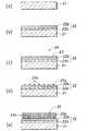
図4の模式的断面図を参照して、本発明に基づくカーボンナノチューブ形成方法の具体例を以下に示す。成膜のための装置としては、図3に示したものを用いた。
【0031】
鏡面研磨したシリコン(Si(100))からなる基板21を硫酸過酸化水素で10分洗浄した後、水洗いし、更に、緩衝フッ化水素酸(buffered hydrofluoric acid:BHF)にて酸化膜を除去し、乾燥した。(図4(a))。次に、清浄化したシリコン基板21上に、6×10−5Paの圧力下で、抵抗加熱蒸着を用いて1nm/秒のレートで50nm厚のチタン(Ti)膜22aを形成し、さらにその上に、Ar分圧5×10−3Torr(6.7×10−4Pa)の下、RFスパッタを用いて0.5nm/秒のレートで100nm厚のタングステン(W)膜22bを形成した(図4(b))。RFスパッタはタングステンのような比較的高融点の材料を成膜するのに適している。これらチタン膜22a及びタングステン膜22bは導電膜22をなす。続いて、1×10−4Paの圧力下で、電子ビーム(EB)蒸着を用い、タングステン膜22b上に鉄(Fe)を0.1nm/秒のレートで蒸着して、鉄(Fe)からなる触媒層23を5nm厚に形成した(図4(c))。電子ビーム蒸着は鉄のような比較的低融点の材料を成膜するのに適している。このようにシリコン基板10上に導電層22及び触媒層23を形成して得られた基体24を、図3に示した熱CVD装置10の石英管12内に置いた石英ホルダー14にセットした。石英管12の内径は30mmであった。そうして、石英管12内にヘリウムガスを250sccmの流量で流し、炉16の温度を概ね700℃に設定した。炉16の温度が概ね700℃になったところから5〜30分維持し、基体24表面の鉄23を微粒子化し、複数の鉄粒子23aを有する構造とした(図4(d))。
【0032】
図5に加熱温度を変えた場合の表面の鉄粒子23aの様子を示す写真を示す。図5(a)に示すように、加熱温度が700℃より低い600℃の場合、鉄の微粒子化が十分に進行せず、また、図5(c)に示すように、加熱温度が700℃より高い800℃の場合も、鉄粒子が粗大化し、微粒子化が十分になされなかった。本実施例では、図5(b)に示すように、加熱温度700℃のとき、表面の鉄の微粒子化が最適になされた。このように本実施例では、加熱温度を概ね700℃にすることが、触媒層23の微粒子化において好適であった。ただし、触媒金属の微粒子化は、触媒層23の厚さ、下地導電層22の濡れ性や形態、加熱時間なども関連するため、最適な加熱温度はそれらの影響で変動し得る。
【0033】
触媒層23の鉄の微粒子化を行った後、ヘリウムの流量を200sccmに減らすとともに、アセチレン(C2H2)を30sccmの流量で導入した。約15分の処理で約30μmの厚さの多層ナノチューブ(multiwall nanotube:MWNT)25が形成された(図4(e))。その後、アセチレンの導入を停止し、ヘリウムを流しつつ室温まで冷却した後、MWNT25が成膜された基体24を取り出し、大気中で700℃で5分処理してアモルファス炭素を除去した。これにより隙間のあるカーボンナノチューブ構造体が形成された。できあがったカーボンナノチューブは直径10〜50nmのMWNTで、基板に対して垂直な方向に繊維が延びて膜を形成した。
【0034】
【発明の効果】
以上説明したように、本発明によると、カーボンナノチューブ形成時に触媒として働く金属または合金からなる触媒層を導電性材料上に形成した後、不活性ガスを供給しつつ所定温度に維持することにより容易に且つ信頼度高く触媒層の金属または合金を微粒子化することができ、そうして得られた触媒粒子の働きにより導電性材料上にカーボンナノチューブを効率的に形成することができる。
【0035】
本発明を実施例に基づいて詳細に説明したが、これらの実施例はあくまでも例示であって本発明は実施例によって限定されるものではない。当業者であれば特許請求の範囲によって定められる本発明の技術的思想を逸脱することなく様々な変形若しくは変更が可能であることは言うまでもない。
【図面の簡単な説明】
【図1】本発明に基づくカーボンナノチューブ膜形成方法の好適実施例を示すフロー図。
【図2】本発明に基づくカーボンナノチューブ膜形成方法を説明するための模式的な断面図。
【図3】本発明に基づくカーボンナノチューブ膜形成方法で用いることのできるカーボンナノチューブ膜製造装置の模式的断面図。
【図4】本発明に基づくカーボンナノチューブ膜形成方法の具体的な実施例を説明するための模式的断面図。
【図5】加熱温度を変えた場合に得られる鉄粒子の状態を示す写真。
【符号の説明】
1 無機質基板
2 導電層
3 触媒層
3a 金属または合金粒子(触媒粒子)
4 基体
5 カーボンナノチューブ膜
10 カーボンナノチューブ製造装置
12 石英管
14 石英ホルダー
16 電気炉
21 シリコン基板
22a チタン膜
22b タングステン膜
22 導電膜
23 触媒(鉄)層
23a 鉄粒子
24 基体
25 多層ナノチューブ(MWNT)[0001]
BACKGROUND OF THE INVENTION
The present invention relates to a method for producing a carbon-based thin film used in a small fuel cell (FC) or the like. In particular, it relates to a method for forming carbon nanotubes (CNT) on a conductive material.
[0002]
[Prior art]
The carbon nanotube is a cylindrical tube made of carbon and having a diameter on the order of nanometers, and is expected to be applied in various applications because of its excellent characteristics. For example, Japanese Patent Laid-Open No. 2002-141084 discloses that in a fuel cell, a carbon film made of carbon nanotubes is used as a support for supporting a catalyst such as platinum. Since carbon nanotubes are porous, they also function as a gas diffusion layer. In the invention disclosed in this publication, a carbon nanotube film is formed on an iron or nickel film formed on an electrode terminal film made of gold or the like, and a platinum catalyst is deposited on the surface thereof by sputtering.
[0003]
As a method of forming the carbon nanotube, there are a method using arc discharge and a method using heating. For example, Japanese Patent Laid-Open No. 2001-58805 discloses, as a method for easily producing a large amount of carbon nanotubes, mixing fullerene molecules and a transition metal element or an alloy containing a transition metal element and heating on a ceramic board. Has been. However, this publication does not describe the formation of carbon nanotubes on conductive materials.
[0004]
In addition, it is known to use as a catalyst a finely divided transition metal such as iron or nickel in the formation of carbon nanotubes. As a method for forming such metal fine particles, there are a method in which a metal thin film is etched with a laser or microwave, and a method in which pores such as zeolite or porous silicon are filled.
[0005]
[Problems to be solved by the invention]
The main objective of the present invention is to provide an improved method for forming carbon nanotubes on a conductive material.
[0006]
The second object of the present invention is to provide a carbon nanotube forming method capable of obtaining metal fine particles that act as a catalyst when growing carbon nanotubes at low cost and efficiently by a simple process.
[0007]
A third object of the present invention is to provide a method for forming carbon nanotubes suitable for use in small fuel cells.
[0008]
[Means for Solving the Problems]
In order to achieve the above object, according to the present invention, a method of forming a carbon nanotube (5) on a conductive material (2), the catalyst layer comprising a metal or alloy that acts as a catalyst when growing the carbon nanotube (3) forming a carbon nanotube on a conductive material using the process of forming a metal or alloy in the catalyst layer, forming a fine particle by treating the metal or alloy of the catalyst layer, and using the metal or alloy fine particle (3a) as a catalyst A process of treating the metal or alloy of the catalyst layer into a fine particle and heating the catalyst layer formed on the conductive material at a predetermined temperature while supplying an inert gas. A method of forming a carbon nanotube is provided. In this way, metal or alloy fine particles that act as a catalyst when growing carbon nanotubes can be easily and inexpensively formed by a simple process, and by using them as a catalyst, carbon nanotubes can be formed on a conductive material. It can be formed efficiently.
[0009]
The catalyst layer preferably contains any one of Fe, Ni, Co, Mo, or an alloy thereof. The conductive material may include at least one of Ti, Au, Ni, Co, Cu, Al, Mo, W, or Ta. The inert gas may be helium or argon.
[0010]
The predetermined temperature at which the metal or alloy of the catalyst layer is atomized is preferably in the range of 0.49 Tm to 0.59 Tm, where Tm is the melting point represented by the absolute temperature of the metal or alloy. When the catalyst layer is made of iron, the temperature is preferably about 700 ° C. If the heating temperature is too low or too high, the particles become coarse and the desired particle size cannot be obtained. The fine particles of metal or alloy preferably have a particle size of 0.5 to 50 nm. Such a particle size has sufficient catalytic action in the formation of carbon nanotubes and can be easily obtained by the above method. By finely pulverizing the metal or alloy of the catalyst layer at the above heating temperature, such a particle size can be efficiently formed by a simple process.
[0011]
If the process of forming the carbon nanotube includes a process of supplying a mixed gas containing a hydrocarbon gas (raw material gas) and an inert gas in the range of 1: 2 to 1:50, amorphous carbon other than the carbon nanotube or It is preferable because carbon nanotubes can be efficiently generated while preventing the growth rate of carbon nanotubes from being extremely slow while suppressing the generation of soot.
[0012]
The flow rate of the mixed gas to be supplied is preferably 1 to 100 cm / min, and particularly preferably 30 cm / min. Thereby, while suppressing the formation of soot, the amount of the source gas discharged without contributing to the formation of the carbon nanotubes can be reduced and the productivity can be improved. When the process of forming the carbon nanotube is performed by placing a conductive material having finely divided metal or alloy in a tube having an inner diameter of approximately 30 mm, the flow rate of the mixed gas flowing in the tube may be approximately 200 to 300 sccm. .
[0013]
In addition, the conductive material can be attached on an inorganic material substrate such as silicon or glass. For example, the conductive material may have a two-layer structure including a layer made of titanium (Ti) and a layer made of tungsten (W) having excellent heat resistance formed thereon. Instead of titanium, aluminum (Al), nickel (Ni), or chromium (Cr) can be used instead. Further, molybdenum (Mo) or tantalum (Ta) can be used instead of tungsten.
[0014]
The features, objects, and advantages of the present invention will become more apparent from the following description of preferred embodiments with reference to the accompanying drawings.
[0015]
DETAILED DESCRIPTION OF THE INVENTION
Hereinafter, preferred embodiments of the present invention will be described with reference to the drawings.
[0016]
FIG. 1 is a flow chart showing a preferred embodiment of the carbon nanotube formation method according to the present invention, and FIG. 2 is a schematic cross-sectional view showing states in several steps of the flow chart of FIG.
[0017]
In
[0018]
Subsequently, in
[0019]
In
[0020]
Referring now to FIG. 3, there is shown a schematic longitudinal sectional view showing a suitable manufacturing apparatus for processing the
[0021]
Please refer to FIG. 1 again. According to the present invention, in
[0022]
The optimum heating temperature in the pretreatment can vary depending on the metal or alloy of the
[0023]
When the pretreatment is completed, the flow rate of the inert gas is reduced in
[0024]
In the carbon nanotube formation process as described above, if the flow rate of the source gas is too large, amorphous carbon or soot other than the carbon nanotubes is generated, the growth of the carbon nanotubes is inhibited, and the ratio of the carbon nanotubes in the
[0025]
The speed (flow rate) of the mixed gas composed of the inert gas and the raw material gas flowing on the surface of the
[0026]
In addition, if the flow rates of the source gas and carrier gas (inert gas) are kept constant during film formation, the carbon nanotubes grow side by side perpendicular to the substrate, but the carbon nanotubes are bent by slightly changing the flow rate. Can be grown. As a result, entanglement between the carbon nanotube fibers occurs, so that the self-supporting strength of the
[0027]
When the film formation is completed, the introduction of the raw material gas is stopped in Step 6, and it is cooled to around room temperature while flowing an inert gas. Further, the
[0028]
Thus, according to the present invention, the metal or alloy of the
[0029]
When the
[0030]
【Example】
A specific example of the carbon nanotube formation method according to the present invention will be described below with reference to the schematic cross-sectional view of FIG. As an apparatus for film formation, the apparatus shown in FIG. 3 was used.
[0031]
The
[0032]
FIG. 5 shows a photograph showing the state of the
[0033]
After atomization of iron in the
[0034]
【The invention's effect】
As described above, according to the present invention, after forming a catalyst layer made of a metal or an alloy that acts as a catalyst when forming carbon nanotubes on a conductive material, it can be easily maintained by supplying an inert gas and maintaining it at a predetermined temperature. In addition, the metal or alloy of the catalyst layer can be made fine particles with high reliability, and the carbon nanotubes can be efficiently formed on the conductive material by the action of the catalyst particles thus obtained.
[0035]
Although the present invention has been described in detail based on examples, these examples are merely examples, and the present invention is not limited to the examples. It goes without saying that those skilled in the art can make various modifications or changes without departing from the technical idea of the present invention defined by the claims.
[Brief description of the drawings]
FIG. 1 is a flowchart showing a preferred embodiment of a carbon nanotube film forming method according to the present invention.
FIG. 2 is a schematic cross-sectional view for explaining a carbon nanotube film forming method according to the present invention.
FIG. 3 is a schematic cross-sectional view of a carbon nanotube film manufacturing apparatus that can be used in the carbon nanotube film forming method according to the present invention.
FIG. 4 is a schematic cross-sectional view for explaining a specific example of the carbon nanotube film forming method according to the present invention.
FIG. 5 is a photograph showing the state of iron particles obtained when the heating temperature is changed.
[Explanation of symbols]
1
4
Claims (6)
Translated fromJapaneseシリコン基板上に、Ti、Ni、AlまたはCrからなる第1の導電層を形成する過程と、
前記第1の導電層上に、W、MoまたはTaからなる第2の導電層を形成する過程と、
カーボンナノチューブを成長させる際に触媒として働く金属または合金を含む触媒層を前記第2の導電層上に形成する過程と、
前記触媒層の金属または合金を処理して微粒子化する過程と、
前記金属または合金の微粒子を触媒として前記第2の導電層上に前記カーボンナノチューブを形成する過程とを有し、
前記触媒層の金属または合金を処理して微粒子化する過程が、不活性ガスを供給しつつ、前記第2の導電層上に形成された前記触媒層を加熱する過程を有することを特徴とするカーボンナノチューブの形成方法。A method of forming carbon nanotubes on a conductive material,
Forming a first conductive layer made of Ti, Ni, Al or Cr on a silicon substrate;
Forming a second conductive layer made of W, Mo or Ta on the first conductive layer;
A process of forming a catalyst layer comprising a metal or alloy acts as a catalyst in thesecond conductivelayer when growing the carbon nanotubes,
A process of treating the metal or alloy of the catalyst layer into fine particles;
Forming the carbon nanotubes onthe second conductivelayer using the metal or alloy fine particles as a catalyst,
And characterized in that it has a process of atomization processes the metal or alloy of the catalytic layer, while supplying an inert gas, thesecond of the catalyst layerpressurized heat process that is formed on the conductivelayer A method of forming carbon nanotubes.
Priority Applications (7)
| Application Number | Priority Date | Filing Date | Title |
|---|---|---|---|
| JP2002182468AJP3877302B2 (en) | 2002-06-24 | 2002-06-24 | Method for forming carbon nanotube |
| PCT/JP2003/005628WO2004000728A1 (en) | 2002-06-24 | 2003-05-02 | Method for making carbon nanotubes |
| US10/520,242US20060141153A1 (en) | 2002-06-24 | 2003-05-02 | Method for making carbon nanotubes |
| DE60322537TDE60322537D1 (en) | 2002-06-24 | 2003-05-02 | METHOD FOR PRODUCING CARBON NANOTUBES |
| CA002490074ACA2490074C (en) | 2002-06-24 | 2003-05-02 | Method for making carbon nanotubes |
| KR1020047020982AKR100671444B1 (en) | 2002-06-24 | 2003-05-02 | Method for making carbon nanotubes |
| EP03728024AEP1519896B1 (en) | 2002-06-24 | 2003-05-02 | Method for making carbon nanotubes |
Applications Claiming Priority (1)
| Application Number | Priority Date | Filing Date | Title |
|---|---|---|---|
| JP2002182468AJP3877302B2 (en) | 2002-06-24 | 2002-06-24 | Method for forming carbon nanotube |
Publications (2)
| Publication Number | Publication Date |
|---|---|
| JP2004026532A JP2004026532A (en) | 2004-01-29 |
| JP3877302B2true JP3877302B2 (en) | 2007-02-07 |
Family
ID=29996655
Family Applications (1)
| Application Number | Title | Priority Date | Filing Date |
|---|---|---|---|
| JP2002182468AExpired - Fee RelatedJP3877302B2 (en) | 2002-06-24 | 2002-06-24 | Method for forming carbon nanotube |
Country Status (7)
| Country | Link |
|---|---|
| US (1) | US20060141153A1 (en) |
| EP (1) | EP1519896B1 (en) |
| JP (1) | JP3877302B2 (en) |
| KR (1) | KR100671444B1 (en) |
| CA (1) | CA2490074C (en) |
| DE (1) | DE60322537D1 (en) |
| WO (1) | WO2004000728A1 (en) |
Families Citing this family (63)
| Publication number | Priority date | Publication date | Assignee | Title |
|---|---|---|---|---|
| WO2004109837A2 (en)* | 2002-10-31 | 2004-12-16 | Carbon Nanotechnologies, Inc. | Fuel cell electrode comprising carbon nanotubes |
| FR2851737B1 (en)* | 2003-02-28 | 2006-05-26 | Commissariat Energie Atomique | CATALYST STRUCTURE, IN PARTICULAR FOR THE PRODUCTION OF FIELD EMISSION DISPLAY SCREENS |
| JP4133655B2 (en)* | 2003-07-02 | 2008-08-13 | 独立行政法人科学技術振興機構 | Method for producing nanocarbon material and method for producing wiring structure |
| JP2005259600A (en)* | 2004-03-12 | 2005-09-22 | Nano Giken Kk | Efficient electronic emitter and its manufacturing method |
| JP2005294109A (en)* | 2004-04-01 | 2005-10-20 | Toyota Motor Corp | FUEL CELL SUBSTRATE AND FUEL CELL |
| JP5374801B2 (en) | 2004-08-31 | 2013-12-25 | 富士通株式会社 | Forming body and forming method of linear structure substance made of carbon element |
| US20060078489A1 (en)* | 2004-09-09 | 2006-04-13 | Avetik Harutyunyan | Synthesis of small and narrow diameter distributed carbon single walled nanotubes |
| US20060048798A1 (en)* | 2004-09-09 | 2006-03-09 | Honeywell International Inc. | Methods of cleaning optical substrates |
| US7348592B2 (en)* | 2004-11-29 | 2008-03-25 | The United States Of America As Represented By The Secretary Of The Navy | Carbon nanotube apparatus and method of carbon nanotube modification |
| KR20060091521A (en) | 2005-02-15 | 2006-08-21 | 삼성에스디아이 주식회사 | Formation method of carbon nanotube and manufacturing method of field emission device using same |
| CA2602599A1 (en) | 2005-03-29 | 2006-10-19 | Hyperion Catalysis International, Inc. | Method for preparing single walled carbon nanotubes from a metal layer |
| JP5349956B2 (en)* | 2005-04-25 | 2013-11-20 | スモルテック エービー | Controlled growth of nanostructures on substrates and electron-emitting devices based thereon |
| US8093715B2 (en)* | 2005-08-05 | 2012-01-10 | Purdue Research Foundation | Enhancement of thermal interface conductivities with carbon nanotube arrays |
| JP2007091481A (en)* | 2005-09-26 | 2007-04-12 | Sonac Kk | Method for production of carbon nanofiber, and production apparatus for carrying out the method |
| FR2896493B1 (en)* | 2006-01-23 | 2008-02-22 | Commissariat Energie Atomique | METHOD FOR PRODUCING A SUPPORT FOR THE GROWTH OF LOCALIZED LONG NANOSTRUCTURES |
| WO2008054839A2 (en)* | 2006-03-03 | 2008-05-08 | William Marsh Rice University | Carbon nanotube diameter selection by pretreatment of metal catalysts on surfaces |
| CN101454242B (en)* | 2006-03-29 | 2012-04-11 | 海珀里昂催化国际有限公司 | Method for preparing single-walled carbon nanotubes from metal layer |
| WO2007117503A2 (en) | 2006-04-07 | 2007-10-18 | The Trustees Of Columbia University In The City Of New York | Preparing nanoparticles and carbon nanotubes |
| US20100117764A1 (en)* | 2006-04-17 | 2010-05-13 | Board Of Regents, The University Of Texas System | Assisted selective growth of highly dense and vertically aligned carbon nanotubes |
| KR100806129B1 (en)* | 2006-08-02 | 2008-02-22 | 삼성전자주식회사 | Method of Forming Carbon Nanotubes |
| JP4948939B2 (en)* | 2006-08-31 | 2012-06-06 | アオイ電子株式会社 | Carbon nanotube synthesis method, silicon substrate, electron source, and field emission display |
| US20080280067A1 (en)* | 2007-05-10 | 2008-11-13 | Feng Chia University | Method of forming a carbon film on a metal substrate at a low temperature |
| US8367506B2 (en) | 2007-06-04 | 2013-02-05 | Micron Technology, Inc. | High-k dielectrics with gold nano-particles |
| JP2009009815A (en)* | 2007-06-28 | 2009-01-15 | Toyota Central R&D Labs Inc | ELECTRODE CATALYST SUBSTRATE, PROCESS FOR PRODUCING THE SAME, AND SOLID POLYMER FUEL CELL |
| US20100279029A1 (en)* | 2007-10-12 | 2010-11-04 | Atomic Energy Council - Institute Of Nuclear Energy Research | Method for coating nanometer particles |
| CN101458599B (en)* | 2007-12-14 | 2011-06-08 | 清华大学 | Touch screen, method for producing the touch screen, and display device using the touch screen |
| CN101458606B (en)* | 2007-12-12 | 2012-06-20 | 清华大学 | Touch screen, method for producing the touch screen, and display device using the touch screen |
| CN101458975B (en) | 2007-12-12 | 2012-05-16 | 清华大学 | Electronic element |
| JP5081637B2 (en)* | 2008-01-11 | 2012-11-28 | 日立造船株式会社 | How to recycle used substrates |
| US8845996B2 (en) | 2008-07-29 | 2014-09-30 | Honda Motor Co., Ltd. | Preferential growth of single-walled carbon nanotubes with metallic conductivity |
| US20100178568A1 (en)* | 2009-01-13 | 2010-07-15 | Nokia Corporation | Process for producing carbon nanostructure on a flexible substrate, and energy storage devices comprising flexible carbon nanostructure electrodes |
| US9406985B2 (en)* | 2009-01-13 | 2016-08-02 | Nokia Technologies Oy | High efficiency energy conversion and storage systems using carbon nanostructured materials |
| CN101924816B (en) | 2009-06-12 | 2013-03-20 | 清华大学 | Flexible mobile phone |
| JP5783669B2 (en)* | 2009-07-23 | 2015-09-24 | ニッタ株式会社 | Method for forming catalytic metal fine particles |
| US9005806B2 (en) | 2009-10-15 | 2015-04-14 | Nokia Corporation | Nano-structured lithium-sulfur battery and method of making same |
| WO2011084756A2 (en)* | 2009-12-21 | 2011-07-14 | 4Wind Science And Engineering, Llc | High performance carbon nanotube energy storage device |
| JP5028502B2 (en)* | 2010-01-22 | 2012-09-19 | 株式会社豊田中央研究所 | Mold, solidified body and production method thereof |
| JP2011178631A (en)* | 2010-03-02 | 2011-09-15 | Nagoya Univ | Method for producing carbon nanotube, single crystal substrate for producing carbon nanotube, and carbon nanotube |
| JP5640494B2 (en)* | 2010-06-23 | 2014-12-17 | トヨタ自動車株式会社 | Manufacturing method of fuel cell |
| KR101903714B1 (en) | 2010-10-18 | 2018-10-05 | 스몰텍 에이비 | Nanostructure device and method for manufacturing nanostructures |
| JP5440487B2 (en)* | 2010-12-20 | 2014-03-12 | トヨタ自動車株式会社 | Manufacturing method of fuel cell |
| EP3269845B1 (en) | 2011-03-26 | 2019-08-14 | Honda Motor Co., Ltd. | Method which produces hydrocarbon transportation fuels |
| CN102185128B (en)* | 2011-04-02 | 2012-11-28 | 上海交通大学 | Silicon-carbon composite material and preparation method thereof |
| JP2014220107A (en)* | 2013-05-08 | 2014-11-20 | 株式会社ワイヤードジャパン | Magnesium-air battery and method of manufacturing cathode thereof |
| FR3006237B1 (en)* | 2013-05-28 | 2015-06-26 | Commissariat Energie Atomique | ELECTRICALLY CONDUCTIVE SUBSTRATE ON AT LEAST ONE OF ITS FACES PROVIDED WITH A THIN LAYER STACK FOR THE GROWTH OF CARBON NANOTUBES (CNT) |
| CA3200272A1 (en) | 2015-12-16 | 2017-06-22 | 6K Inc. | Spheroidal dehydrogenated metals and metal alloy particles |
| US10987735B2 (en) | 2015-12-16 | 2021-04-27 | 6K Inc. | Spheroidal titanium metallic powders with custom microstructures |
| FR3079674A1 (en)* | 2018-03-29 | 2019-10-04 | Commissariat A L'energie Atomique Et Aux Energies Alternatives | COLLECTOR PLATE FOR LOW THICK FUEL CELL |
| EP3810358A1 (en) | 2018-06-19 | 2021-04-28 | 6K Inc. | Process for producing spheroidized powder from feedstock materials |
| CA3134573A1 (en) | 2019-04-30 | 2020-11-05 | Sunil Bhalchandra BADWE | Mechanically alloyed powder feedstock |
| ES2994209T3 (en) | 2019-11-18 | 2025-01-20 | 6K Inc | Unique feedstocks for spherical powders and methods of manufacturing |
| US11590568B2 (en) | 2019-12-19 | 2023-02-28 | 6K Inc. | Process for producing spheroidized powder from feedstock materials |
| EP4173060A1 (en) | 2020-06-25 | 2023-05-03 | 6K Inc. | Microcomposite alloy structure |
| WO2022067303A1 (en) | 2020-09-24 | 2022-03-31 | 6K Inc. | Systems, devices, and methods for starting plasma |
| EP4237174A1 (en) | 2020-10-30 | 2023-09-06 | 6K Inc. | Systems and methods for synthesis of spheroidized metal powders |
| CA3197544A1 (en) | 2021-01-11 | 2022-07-14 | 6K Inc. | Methods and systems for reclamation of li-ion cathode materials using microwave plasma processing |
| US12042861B2 (en) | 2021-03-31 | 2024-07-23 | 6K Inc. | Systems and methods for additive manufacturing of metal nitride ceramics |
| SE545845C2 (en)* | 2021-07-09 | 2024-02-20 | Smoltek Ab | A separator plate arrangement for an electrochemical cell comprising a nanostructure |
| WO2023229928A1 (en) | 2022-05-23 | 2023-11-30 | 6K Inc. | Microwave plasma apparatus and methods for processing materials using an interior liner |
| US12040162B2 (en) | 2022-06-09 | 2024-07-16 | 6K Inc. | Plasma apparatus and methods for processing feed material utilizing an upstream swirl module and composite gas flows |
| CN114933296B (en)* | 2022-06-20 | 2024-08-30 | 瞿金虎 | Carbon nanotube and method for preparing same |
| US12094688B2 (en) | 2022-08-25 | 2024-09-17 | 6K Inc. | Plasma apparatus and methods for processing feed material utilizing a powder ingress preventor (PIP) |
| US12195338B2 (en) | 2022-12-15 | 2025-01-14 | 6K Inc. | Systems, methods, and device for pyrolysis of methane in a microwave plasma for hydrogen and structured carbon powder production |
Family Cites Families (8)
| Publication number | Priority date | Publication date | Assignee | Title |
|---|---|---|---|---|
| US5641466A (en)* | 1993-06-03 | 1997-06-24 | Nec Corporation | Method of purifying carbon nanotubes |
| AUPP976499A0 (en)* | 1999-04-16 | 1999-05-06 | Commonwealth Scientific And Industrial Research Organisation | Multilayer carbon nanotube films |
| US6361861B2 (en)* | 1999-06-14 | 2002-03-26 | Battelle Memorial Institute | Carbon nanotubes on a substrate |
| US6062931A (en)* | 1999-09-01 | 2000-05-16 | Industrial Technology Research Institute | Carbon nanotube emitter with triode structure |
| EP1129990A1 (en)* | 2000-02-25 | 2001-09-05 | Lucent Technologies Inc. | Process for controlled growth of carbon nanotubes |
| US6755956B2 (en)* | 2000-10-24 | 2004-06-29 | Ut-Battelle, Llc | Catalyst-induced growth of carbon nanotubes on tips of cantilevers and nanowires |
| GB0109546D0 (en)* | 2001-04-18 | 2001-06-06 | Va Tech Transmission & Distrib | Vacuum power switches |
| US6858197B1 (en)* | 2002-03-13 | 2005-02-22 | The United States Of America As Represented By The Administrator Of The National Aeronautics And Space Administration | Controlled patterning and growth of single wall and multi-wall carbon nanotubes |
- 2002
- 2002-06-24JPJP2002182468Apatent/JP3877302B2/ennot_activeExpired - Fee Related
- 2003
- 2003-05-02USUS10/520,242patent/US20060141153A1/ennot_activeAbandoned
- 2003-05-02WOPCT/JP2003/005628patent/WO2004000728A1/enactiveIP Right Grant
- 2003-05-02DEDE60322537Tpatent/DE60322537D1/ennot_activeExpired - Lifetime
- 2003-05-02EPEP03728024Apatent/EP1519896B1/ennot_activeExpired - Lifetime
- 2003-05-02KRKR1020047020982Apatent/KR100671444B1/ennot_activeExpired - Fee Related
- 2003-05-02CACA002490074Apatent/CA2490074C/ennot_activeExpired - Fee Related
Also Published As
| Publication number | Publication date |
|---|---|
| JP2004026532A (en) | 2004-01-29 |
| EP1519896B1 (en) | 2008-07-30 |
| CA2490074C (en) | 2008-04-29 |
| CA2490074A1 (en) | 2003-12-31 |
| KR100671444B1 (en) | 2007-01-19 |
| DE60322537D1 (en) | 2008-09-11 |
| EP1519896A1 (en) | 2005-04-06 |
| US20060141153A1 (en) | 2006-06-29 |
| KR20050016623A (en) | 2005-02-21 |
| WO2004000728A1 (en) | 2003-12-31 |
Similar Documents
| Publication | Publication Date | Title |
|---|---|---|
| JP3877302B2 (en) | Method for forming carbon nanotube | |
| JP4379247B2 (en) | Method for producing carbon nanostructure | |
| JP3819382B2 (en) | Carbon nanotube matrix and growth method thereof | |
| US6764874B1 (en) | Method for chemical vapor deposition of single walled carbon nanotubes | |
| JP4272700B2 (en) | Nanostructure and manufacturing method thereof | |
| JP3804594B2 (en) | Catalyst supporting substrate, carbon nanotube growth method using the same, and transistor using carbon nanotubes | |
| US20110014368A1 (en) | Carbon nanotube growth at reduced temperature via catalytic oxidation | |
| KR20060094958A (en) | Method for controlling the diameter of carbon nanotubes, carbon nanotubes or carbon nanotube arrays and structures including the same, field effect transistors and integrated circuits including the same | |
| US20040081758A1 (en) | Ccvd method for producing tubular carbon nanofibers | |
| WO2007116434A1 (en) | Process for producing carbon nanotube | |
| JP2017019718A (en) | Manufacturing method of carbon nano-tube | |
| JP4834957B2 (en) | Catalyst structure and carbon nanotube production method using the same | |
| JP2004284921A (en) | Method for producing carbon nanotube, carbon nanotube device and electric double layer capacitor | |
| JP3913583B2 (en) | Method for producing carbon nanotube | |
| JP2004051432A (en) | Substrate for producing carbon nanotube and method for producing carbon nanotube using the same | |
| Hofmeister et al. | Carbon nanotube growth from Cu–Co alloys for field emission applications | |
| JP2005126323A (en) | Catalyst carrying substrate, method for growing carbon nanotube using the same, and transistor using the carbon nanotube | |
| JP2008297174A (en) | Method for manufacturing carbon nanotube growth substrate | |
| JP2007254167A (en) | Method for production of carbon nanotube | |
| JP3958330B2 (en) | Carbon nanotube device and manufacturing method thereof | |
| JP2010116305A (en) | Process of producing carbon nanotube and base material for growing carbon nanotube | |
| JP2010116279A (en) | Method for producing nano carbon material |
Legal Events
| Date | Code | Title | Description |
|---|---|---|---|
| A621 | Written request for application examination | Free format text:JAPANESE INTERMEDIATE CODE: A621 Effective date:20050425 | |
| A131 | Notification of reasons for refusal | Free format text:JAPANESE INTERMEDIATE CODE: A131 Effective date:20060815 | |
| A521 | Request for written amendment filed | Free format text:JAPANESE INTERMEDIATE CODE: A523 Effective date:20060925 | |
| TRDD | Decision of grant or rejection written | ||
| A01 | Written decision to grant a patent or to grant a registration (utility model) | Free format text:JAPANESE INTERMEDIATE CODE: A01 Effective date:20061024 | |
| A61 | First payment of annual fees (during grant procedure) | Free format text:JAPANESE INTERMEDIATE CODE: A61 Effective date:20061030 | |
| R150 | Certificate of patent or registration of utility model | Free format text:JAPANESE INTERMEDIATE CODE: R150 | |
| FPAY | Renewal fee payment (event date is renewal date of database) | Free format text:PAYMENT UNTIL: 20091110 Year of fee payment:3 | |
| FPAY | Renewal fee payment (event date is renewal date of database) | Free format text:PAYMENT UNTIL: 20101110 Year of fee payment:4 | |
| FPAY | Renewal fee payment (event date is renewal date of database) | Free format text:PAYMENT UNTIL: 20101110 Year of fee payment:4 | |
| FPAY | Renewal fee payment (event date is renewal date of database) | Free format text:PAYMENT UNTIL: 20111110 Year of fee payment:5 | |
| FPAY | Renewal fee payment (event date is renewal date of database) | Free format text:PAYMENT UNTIL: 20111110 Year of fee payment:5 | |
| FPAY | Renewal fee payment (event date is renewal date of database) | Free format text:PAYMENT UNTIL: 20121110 Year of fee payment:6 | |
| FPAY | Renewal fee payment (event date is renewal date of database) | Free format text:PAYMENT UNTIL: 20131110 Year of fee payment:7 | |
| R250 | Receipt of annual fees | Free format text:JAPANESE INTERMEDIATE CODE: R250 | |
| R250 | Receipt of annual fees | Free format text:JAPANESE INTERMEDIATE CODE: R250 | |
| R250 | Receipt of annual fees | Free format text:JAPANESE INTERMEDIATE CODE: R250 | |
| LAPS | Cancellation because of no payment of annual fees |