JP3877058B2 - Small apparatus and manufacturing method thereof - Google Patents
Small apparatus and manufacturing method thereofDownload PDFInfo
- Publication number
- JP3877058B2 JP3877058B2JP2001516128AJP2001516128AJP3877058B2JP 3877058 B2JP3877058 B2JP 3877058B2JP 2001516128 AJP2001516128 AJP 2001516128AJP 2001516128 AJP2001516128 AJP 2001516128AJP 3877058 B2JP3877058 B2JP 3877058B2
- Authority
- JP
- Japan
- Prior art keywords
- light
- image
- angle
- imaging
- lens
- Prior art date
- Legal status (The legal status is an assumption and is not a legal conclusion. Google has not performed a legal analysis and makes no representation as to the accuracy of the status listed.)
- Expired - Fee Related
Links
Images


Classifications
- G—PHYSICS
- G02—OPTICS
- G02B—OPTICAL ELEMENTS, SYSTEMS OR APPARATUS
- G02B17/00—Systems with reflecting surfaces, with or without refracting elements
- G—PHYSICS
- G06—COMPUTING OR CALCULATING; COUNTING
- G06V—IMAGE OR VIDEO RECOGNITION OR UNDERSTANDING
- G06V40/00—Recognition of biometric, human-related or animal-related patterns in image or video data
- G06V40/10—Human or animal bodies, e.g. vehicle occupants or pedestrians; Body parts, e.g. hands
- G06V40/12—Fingerprints or palmprints
- G06V40/13—Sensors therefor
- G06V40/1324—Sensors therefor by using geometrical optics, e.g. using prisms
Landscapes
- Physics & Mathematics (AREA)
- Engineering & Computer Science (AREA)
- Optics & Photonics (AREA)
- General Physics & Mathematics (AREA)
- Human Computer Interaction (AREA)
- Multimedia (AREA)
- Theoretical Computer Science (AREA)
- Image Input (AREA)
- Measurement Of The Respiration, Hearing Ability, Form, And Blood Characteristics Of Living Organisms (AREA)
- Color Television Image Signal Generators (AREA)
- Facsimile Scanning Arrangements (AREA)
Abstract
Description
Translated fromJapanese発明の分野
本発明は、像キャプチャー及び認識システムに使用される光学撮像装置に関し、特に、模様が形成されている物体(patterned object、以下POと称する)の像の台形歪みを軽減あるいは実質的に排除し、該像をより鮮明にする光学撮像装置に関する。
【0001】
従来の技術
PO認識システムは産業的、商業的に一般化され、例えば、文書、絵、写真をスキャンするスキャナなど、様々な用途に使用されている。近年では、一般消費者向けにパターン認識システムの利用を進めるべく、メーカ側では、そのコストダウンが図られている。そうしたパターン認識システムの一般消費者向け製品への利用例の一つが、指紋の撮像及び認識である。これにより、例えばコンピュータの利用者の指紋を採取して、コンピュータの使用もしくは特定のファイル・機能へのアクセスの権限を持つユーザの指紋と比較することで、セキュリティの向上を図ることが可能である。かかるシステムは、例えばログインネーム及びパスワードによるセキュリティシステムの代替物となりうる。
【0002】
まず第一に、このような指紋認識システムおよび他のパターン認識システムでは、解析のために、指紋や他の模様を正確に撮影することが求められる。パターン情報の取得に関しては既に様々なメカニズムが開発されており、例えば、米国特許3,975,711号、4,681,435号、5,051,576号、5,177,435号、及び5,233,404号が、PO像の撮影に関する装置を開示している。
【0003】
図1は、このような従来技術の光学的指紋撮影認識システムを示す概略図である。図1において、光学認識システム108は、光源112、光学三角プリズム110、レンズ体114、イメージセンサ116、格納及び処理ユニット125を含んでいる。プリズム110は、撮像面(imaging surface)118、受光面(light receiving surface)120、および出射面(viewing surface)122を含んでいる。撮像面118は、指紋などのPOが撮像のために置かれる面である。光源112は、例えばLEDであって、受光面120に近接し、光学プリズム110に送られる入射光124を発する。光学プリズム110は直角二等辺三角形になっていて、撮像面118と向かい合う角はほぼ90°であり、他の2つの底角(二等辺三角形の等しい二角)はほぼ45°となっている。
【0004】
一般に、入射光124は撮像面118に、撮像面の法線115に対して角度126で入射する。角度126は臨界角128より大きい。一般に臨界角とは入射する光線と面の法線との間の角度のことを指している。入射光が臨界角よりも大きな角度で入射するときは、入射光は表面で内部全反射(total internal reflection off the surface)され、一方臨界角よりも小さな角度で入射するときには、入射光はほぼすべて表面を通り過ぎる。以上のように、臨界角128とは、入射光が撮像面118で完全に内部反射され、反射光130として出射面122を経由してプリズム120から発射される際の、撮像面118の法線に対する角度のことである。
【0005】
反射光130は、出射面122に近接するレンズ体114を通過する。レンズ体114は、一つ以上の光学レンズを含んでなっていてもよい。レンズ体114からの光はイメージセンサ116によって取り込まれる(captured)。レンズ体114は、例えば光学的に像を取り込んで電気信号に変換する、電気結合素子(CCD:Charged Coupled Device)や相補型MOS(CMOS:Complimentary Metal Oxide Semiconductor)素子であってもよい。このようなイメージセンサは当業者には広く知られているものである。電気信号は、次に格納及び処理ユニット125に送られる。
【0006】
格納及び処理ユニット125は、メモリユニット、プロセッサ、アナログ/デジタルコンバータを含んでいてもよい(図示せず)。アナログ/デジタルコンバータは、イメージセンサ116からのアナログ電気信号をデジタルデータに変換する。メモリは、デジタルデータと、キャプチャーされた指紋の像を格納された指紋像と比較する際のアルゴリズムと、を格納するために用いられる。プロセッサは、データ比較アルゴリズムに基づいて、取り込まれたデジタルデータと事前にメモリに格納されたデータとを比較する。また、プロセッサによって、格納されているデータとの比較以外の目的のために、取り込まれたデジタルデータを解析することもできる。かかる格納及び処理ユニットは当業者には広く知られ、必要なソフトを搭載した一般的なパーソナルコンピュータもこれに該当する。画像データの処理及び比較用アルゴリズムの例としては、米国特許4,135,147号や、同4,688,995号がある。尚、これらの開示内容は、全て本出願に引例として含まれることとする。
【0007】
光学プリズムの撮像面118に指紋が置かれると、指紋の隆部(ridge)111が撮像面118に触れ、指紋の谷部(valley)109は撮像面118に触れない状態を保持する。よって指紋の谷部109では、光源112から光学プリズム110に入る入射光124は、入射角が光学プリズム110の臨界角よりも大きい場合、撮像面118で内部全反射される。一方指紋の隆部111においては、一部の入射光124は、指紋の隆部で吸収されるか散乱する。ここで用いられている「散乱」とは、光が不規則な面に当たった後、多方向に放射されるか、不規則に反射されることを指している。
【0008】
散乱もしくは吸収の結果として、指紋の隆部111では、入射光124が内部全反射されてしまうことがない。よって指紋の谷部109よりプリズム110を離れた反射光130の強度は、指紋の隆部111よりプリズム110を離れた反射光130よりも大きい。隆部111からの強度の小さい反射光130は暗く現れ、光線と指紋表面との間の光入射地点に物体が存在することを示す。これに対し、内部全反射されるような強度の高い反射光130は明るく現れることで、入射光124と撮像面118との間に位置する光入射地点に物体が存在しないことを示す。これにより、暗く現れる指紋の隆部111と比較的明るく現れる指紋の谷部109との区別が可能となる。この理由は、指紋の隆部111での入射光の吸収が、指紋撮像の際の最も重要な要素であるためであり、かかるシステム108は吸収式撮像システムと呼ばれる。
【0009】
上記のシステムでは、光学的に指紋像を取り込み、該指紋像を電気的に表現する処理が可能である。しかし、指紋の隆部111の部分では、依然として入射光124の一部が反射光130に平行な方向に内部全反射し、一部が散乱している。このことにより、指紋の谷部109からの反射光130の強度と、指紋の隆部111からの反射光130の強度との差が、比較的低くなってしまう可能性がある。つまり、指紋像における指紋の谷部109と指紋の隆部111との間のコントラストがはっきりしなくなる可能性がある。これにより、撮像、処理、比較が困難になってしまう。
【0010】
さらに、光学認識システム108のような光学認識システムにおいては、レンズ体114の第一レンズの直径は、出射面122上の指紋像よりも小さいことが望ましい。これにより、光学認識システム108を小型化し、製造コストを低減することが可能となる。
【0011】
しかし、図2に示すように、システム108のような吸収式システムでは、レンズ体114の第一レンズの直径が撮像面118上の指紋よりも小さい場合、レンズ体114が撮像面118から比較的離れた位置に配置される必要がある。この構成により、システム108によって取り込まれた指紋像は、指紋の縁部に至るまで鮮明に表現される。一方で、レンズ体114の配置が出射面122に近過ぎると、指紋像の縁部が失われたり歪んだりすることがある。これは、システム108のような吸収式システムでは、指紋像に焦点を合わせるためには、指紋像を作る光線が略平行でなければならないからである。また、レンズ体114の第1レンズが撮像面118上の指紋よりも小さい場合、指紋像の中央に近い領域からの光線に対して平行になっている指紋像の縁部からの光線がレンズ体114に入らず、よって指紋像の縁部がぼやけたり失われたりする可能性がある。
【0012】
よって、図2に示すように、光学認識システム108のレンズ体が、点線で示されるレンズ体114’の位置にある場合、略平行な反射光130と130’はレンズ体114’に入らない。この理由により、レンズ体がレンズ体114’の位置に配置される場合、システム108では、撮像面118のA点及びB点の指紋像を鮮明に撮影することができない。
【0013】
こうして、図2に示すように、吸収式システムでは、略平行な光線によって指紋像の全体を撮像するためには、レンズ体114を出射面122から比較的遠くに配置しなければならず、それゆえ、レンズ体114の第一レンズを比較的小さくしてシステムの小型化を図った事が無駄になってしまう可能性がある。このように、光学認識システム108の小型化には困難が伴う。さらに、出射面122とレンズ体114との距離が比較的大きいために、光の干渉によって指紋像のコントラストが失われてしまうことも考えられる。
【0014】
加えて、レンズ体114の第一レンズが出射面122上の指紋像より小さい場合、光学認識システム108内で、台形歪みと呼ばれる現象が生じる。撮像システムにおける台形歪みとは、システムで形成された正方形の像が台形のような形に変形されて見えることをいう。
【0015】
図2は、なぜ台形歪みが光学認識システム108において生じるかを説明した概略図である。光源112からの入射光124はプリズム110に入り、撮像面118で反射して、像ABを形成する。そして反射光130は出射面122を通過してレンズ体114に達し、A’地点及びB’地点において像A’B’を形成する。出射面122を通じて見られる像ABは、「見かけ像」(apparent image)として像abに位置しているように見える。具体的には、A地点は出射面122より距離aa’だけ離れたa地点にあるように見え、B地点は出射面122より距離bb’だけ離れたb地点にあるように見える。出射面122から物体の見かけ像が現れる地点までの距離は、出射面122から物体までの実際の距離を、プリズム110の屈折率nで割った値となる。具体的には、距離aa’は次の式で求められる。
【0016】
aa’=Aa’/n
ただし、nはプリズム110の屈折率である。同様に、次式が得られる。
【0017】
bb’=Bb’/n
台形歪みは、物体の見かけ像からレンズ体114のレンズ面107までの光路の長さが像を結んでいる物体の部分によって異なり、レンズ体114の対物レンズが出射面122を通過する指紋像よりも小さい場合に生じる。具体的にいえば、システム108の場合、台形歪みが生じるのは、距離aA’が距離bB’よりも長く、レンズ体114の直径が出射面122上の距離a’b’よりも短い場合である。
【0018】
また、距離aA’が距離bB’よりも長いことから、どの部分においても焦点が合っているような物体の像を得ることが困難になっている。概して、見かけ物体の像からレンズ体のレンズ面までの光路長や、さらに最終的にはイメージセンサまでの光路長が、像を結んでいる物体の部分によって異なる場合には、レンズ面において物体のある部分では焦点が合っており、またある別の部分ではぼやけてしまう。
【0019】
このような台形歪み及び物体の像の一部がぼやけるという問題を解決すべく、従来技術では、レンズ体114のレンズ面107とイメージセンサ116とを傾けて距離bB’を伸ばす一方で距離aA’を小さくし、これら2つの距離がほぼ同じになるように構成している。しかし、直角二等辺プリズム(即ち、底角がほぼ45°、底角でない角、つまりは頂角がほぼ90°である三角プリズム)の特性上、反射光130は出射面122に実質的に垂直にプリズム110を通過する。従って、反射光130が出射面122を通る際には屈折は生じない。更に、一般には、透明な物体の表面への光の入射角が大きいほど、表面で反射される光の量は多くなる。このようにして、イメージセンサ116に入る光の強度が減少し、像の処理および比較がより困難になってしまう。
【0020】
従って、レンズ体114及びセンサを傾けることは、台形ゆがみを低減して像の鮮明さを向上する一方、反射光130が大きな入射角にてレンズ体114に入射するので、レンズ体114表面や、イメージセンサ116表面での反射光130の反射が大きくなってしまう。これにより、イメージセンサ116に入射する光の強度が小さくなり、処理や比較が困難になる。
【0021】
加えて、光源112とレンズ体114の相対的な配置によって、光源112からの迷い光(stray light)113がレンズ体114に入るようになってしまっている。これにより、さらに取り込まれた像の質を低下させ、その像の処理を困難にする、余分なバックグラウンドである「ノイズ光」が発生する。
【0022】
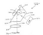
上記のような吸収式撮像システムの問題点を解消すべく、吸収式ではなく「散乱式」による撮像システムが考案されており、その一例が、J.Lougheedらの、1993年8月3日開示の米国特許5,233,404号である。図3は、Lougheedらによる装置の撮像部を示した概略図である。この図3に示すように、従来技術の撮像システム208は、台形プリズム210、光源212、レンズ体214、及びイメージセンサ216を備えている。台形プリズム210は、少なくとも撮像面218、受光面220、出射面222を有している。
【0023】
撮像面218は、指紋など撮像される物体が置かれる面である。光源212は、撮像面218と略平行な受光面220に近接し、対向するように配置されている。よって光源212からの入射光224はプリズム210に入り、プリズム210の臨界角228よりも小さい角度で撮像面218に入射する。従って、指紋の谷部209が撮像面218に置かれている面、即ち指紋が撮像面に接していない面においては内部全反射が起こらず、入射光224は撮像面218を通り抜ける。指紋の隆部211が接して置かれている撮像面218では、入射光224は指紋の隆部で反射して、散乱光(あるいは不規則反射光)230を生ずる。散乱光230は、プリズム210内の、入射面222に近接するレンズ体214への方向を含めたほぼ全ての方向へと広がってゆく。散乱光は入射面222を通りレンズ体214に入って、上記のようなCCD、CMOSといった検出装置であるイメージセンサ216により検出される。
【0024】
指紋の谷部209の領域では、入射光224は撮像面218を通過する。また、指紋の隆部211の領域では、入射光224は撮像面218で散乱して、レンズ体214及びイメージセンサ216によって捕捉される。従って、指紋の隆部211の像は比較的明るく、指紋の谷部209の像は比較的暗くなる。これは散乱光230がイメージセンサ216によって捕捉されるためであり、このタイプのシステムを「散乱」システムといっている。
【0025】
散乱システムにより形成された、指紋像の隆部と谷部との間の光の強度の差あるいは強度の度合いは、図1に示すように、吸収システムにおける、指紋像の隆部と谷部との間の光の強度の差あるいは強度の度合いよりも大きくなっている。これにより、散乱システムによって形成された指紋像の、指紋の隆部と谷部との間のコントラストの方が、吸収システムによるものよりもはっきりしたものになる。こうしてイメージセンサ216がより鮮明な像を捉えられるようになり、該システムによる指紋の比較の精度が向上する。
【0026】
さらに、散乱システムの特性上、レンズ体214に入って指紋の像を形成する光線が平行でなくても鮮明な像が形成される。よって、レンズ体214の第一レンズが入射面222上での指紋の像より小さくても、像の縁部付近での鮮明さを失う事なく、レンズ体214を入射面222の比較的近くに配置することが可能になる。
【0027】
しかし、プリズム210のような台形プリズムは、図1に示すプリズム110のような三角プリズムよりも製造コストが高くなる。その一因は、研磨すべき表面が多くなることに起因する。このような製造コストの増加は撮像システム208のようなシステムの高価格化を招き、一般消費者向け製品への利用をさらに困難にしてしまう。
【0028】
さらに、プリズム210における指紋の見かけ像からレンズ体214までの散乱光の光路長が、像の各部分によって異なることから、撮像システム208では、光学認識システム108の場合と同様に、指紋像の一部分がぼやけてしまうことがある。加えて、図3には示していないが、撮像システム208におけるレンズ体114の第一レンズが入射面222上の指紋像よりも小さい場合、プリズム210における指紋の見かけ像の部分に応じて、像からレンズ体214およびイメージセンサ216までの散乱光の光路長の違いにより、台形歪みも発生する。
【0029】
これまでの記述によって明らかなように、PO認識システム用の撮像装置の改良が望まれている。具体的には、像の台形歪みを軽減もしくは略解消した撮像装置が望まれている。さらに、撮像装置は像のほぼ全ての部分に焦点を合わせられるものが望ましく、また比較的コンパクトで製造コストが安いものが好ましい。
【0030】
発明の概要
本発明は、台形の歪みを低減した、もしくは略解消した、ハイ・コントラスト、ロー・歪みの像を形成する撮像装置を含んでいる。さらに、本発明の撮像システムは比較的低価にて製造できる。撮像装置は、POの見かけ像を形成するために、対象物を配置する撮像面と、さらにもう一つの面と、出射面とを備える光屈折器を有する。出射面は、撮像面に近接し、撮像面に対して角度γをなす。POの像は出射面から映し出される。また、撮像装置は、POの像を受け取ったり、焦点をあわせるための出射面に近接したレンズを備えている。レンズは光軸に対して垂直になるレンズ面を有し、出射面に対して角度δをなす。角度γおよび角度δは、POの見かけ像の一部分からレンズ面までの第一光線の光路長であり、最終的にはイメージセンサまでの光路長と、第一光線に略平行でPOの見かけ像の別の部分からレンズ面までの別の光線の光路長であり、最終的にはイメージセンサまでの光路長と、を実質的に等しくするためになされる角度である。好ましくは、以下の式が成り立つように角度γと角度δを設定すればよい。
【0031】
0.7≦(n2−sin2δ)1/2(cotγ)(sinδ)+sin2δ≦1.30
本発明は、また、出射面と光線とが、出射面の撮像面との交差部の側にて、90°未満の角度をなし、撮像される対象物が置かれる撮像面のどの部分も、少なくとも一つの光線が散乱される構成を有していることが好ましい。
【0032】
本発明の製造方法は、上記小型装置の製造方法であって、光屈折器(310)を形成するステップと、出射面(320)によって定義される平面と、撮像面(318)によって定義される平面との間のゼロにならない角度γ(342)を形成するステップと、光源(312)と、第1遮光部(350)と、第2遮光部(352)とを形成するステップと、前記レンズ面が、当該レンズの中心を通るシステムの光軸に垂直になるように、前記出射面に近接してレンズ(314)を配置するステップと、前記出射面によって定義される平面と前記レンズ面との間のゼロにならない角度δ(343)を形成するステップと、前記見かけ像の一部から前記レンズ面までの第一光線の光路長と、当該第一光線に実質的に平行であり、前記見かけ像の別の部分から前記レンズ面までの別の光線の光路長とが実質的に等しくなるように、角度γと角度δとを設定するステップとを含むことを特徴としている。好ましくは、角度γと角度δは以下の関係が成り立つように設定される。
【0033】
0.7≦(n2−sin2δ)1/2(cotγ)(sinδ)+sin2δ≦1.30
さらに、光線と出射面の交差部が、出射面の撮像面との交差部の側から見て、90°未満の第一角度が形成され、撮像に使用される撮像面のどの部分も、少なくとも一つの光線が散乱される構成を有していることが好ましい。
【0034】
上記の装置および方法により、台形の歪みの少ない、あるいは台形の歪みのない、POを撮像することができ、比較的に焦点のはっきりした像を形成することができる。これにより、POのより正確な処理や比較を有効に促進することが可能になる。
【0035】
発明の詳細な説明
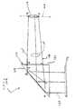
図4および5は本発明に係る模様が形成されている物体(patterned object、以下POと称する)の像を映しだすシステム308を示している。撮像システム308は好ましくは、三角プリズム310、光源312、レンズ体314、およびイメージセンサ316を備えている。プリズム310は、図4を示した紙面に対して垂直な方向に延びる長さを有する、5面体の三角プリズムである。プリズム310は、指紋335などの像を撮ろうとする対象物を配置する平坦な矩形撮像面318を有する。また、プリズム310は、撮像面318に当てた指紋335の像がプリズム310から外部に出る、平坦な矩形出射面(viewing surface)320を有している。図4および5の実施の形態において、出射面320は、プリズム310の内部に光を入射する受光面としての役割も果たす。光散乱面322は、プリズム310の第3またはそれ以上の平坦な矩形面を形成する。以下に詳細する理由で、光散乱面322は拡散面であることが好ましい。
【0036】
光源312は、発光ダイオード(LED)をプリズム310の(図4の紙面に対して垂直な方向に延びる)長さ程度に一列に並べたLEDアレーであることが好ましい。このLEDアレーを光源312として使用すると、拡散蓋体を該LEDアレーと出射面320との間に設けることができ、撮像面318が一層均一に照射される。なお、光源312は、プリズム310に光を入射させられ得る限りどんなタイプの光源であってもよく、そのタイプの如何によらず本発明の範囲内である。プリズム310の、撮像面318の反対に位置するエッジ338に沿って光源312が設けられることが好ましい。また、撮像システム308の光源はこれ以外の構成でもいいし、これ以外の位置に設置してもよく、いずれの場合も本発明の範囲内である。本発明に適用できる光源の例としては、ここに挙げた以外に、同じ譲受人のもとで出願され、現在審査中の米国特許出願09/191,428号(出願日1998年11月12日)、「ハイ・コントラスト、ロー・歪みの映像キャプチャー光学システム」に開示されている。この特許出願の開示内容全体は、本発明に含まれているものとする。一例を挙げると、光源312は、エッジ365から出射面320に降ろした垂線と出射面320との交差部に形成される線360とエッジ338との間であれば、出射面320に対してどこに設置してもかまわない。
【0037】
レンズ体314は、指紋335からの散乱光330を受け、この散乱光330をイメージセンサ316上で集束させるためのものである。レンズ体314は一つのレンズでもよいが、好ましくは、複数のレンズから構成されているのがよい。焦点距離が約13.48mmのレンズ体314を出射面320から約13.5mmの位置に設けるのが最も好ましい。また、レンズ体314の一実施の形態の概略図である図7に示すように、レンズ体は三つのレンズ904、906、908を有し、それぞれの光軸が共通の光軸902に重なっていることが最も好ましい。レンズ904の直径が約17.8mmであり、レンズ906、908の直径は約6mmであることが最も好ましい。レンズ体314はいくつのレンズからなっていても構わない。
【0038】
イメージセンサ316は、レンズ体314から光学的に形成された像を取り込んで(capture)電気信号に変換する。イメージセンサ316は例えば電荷結合素子(CCD)であるが、これに限らず、光信号をアナログあるいはデジタル電気信号に変換する手段であればよい。イメージセンサ316としてはCMOS(complementary metal oxide semiconductor)素子を使用することが好ましい。CCD及びCMOSイメージセンサは当業者によく知られている。イメージセンサ316が形成した電気信号は周知の手段を用いて処理可能であり、指紋などの入力模様を比較するのに用いられる。従来の技術にて言及したように、こういった信号処理方法は、例えば米国特許4,135,147号および4,688,995号に開示されており、この2件の開示内容全体を本発明は含んでいるものとする。
【0039】
イメージセンサ316上に指紋335の像を形成するために、指紋335を撮像面318に当てる。光源312から入射する光324は出射面320を通過してプリズム310に入る。光源312がエッジ338に近接した位置にあるので、入射光324は散乱面322に当たる。前述のように、散乱面322は拡散性があるものがよい。これにより、散乱面322に照射される入射光334のうち、プリズム310内で散乱する割合が比較的高くなる。次に、この散乱光が撮像面318に当たる。たとえ光散乱面322が拡散性を有していなくても、入射光324の略全てが、散乱面322の臨界角より大きい角度323で散乱面322に当たることになる。このように、入射光は、散乱面322で反射して撮像面318に入射する。散乱面322での入射光の反射性を高めるために、反射面381の鏡面が散乱面322に対向するように配置してもよい。
【0040】
入射光324は散乱面322で散乱するかあるいは直接反射するので、入射光324のうち、プリズム310の臨界角328より小さい角度327で撮像面318に入射するものの割合が比較的高くなる。したがって、指紋の谷部309で撮像面318に当たる入射光324は内部に向かって全反射せず、大部分が撮像面318を通過することになる。このように、指紋の谷部309にて、撮像面318に当たる光は、そのほとんどがセンサ316に向かって進まない。一方、撮像面318に指紋の隆部311が触れているところで撮像面318に入射した入射光324は、大部分が散乱して、散乱光330となる。散乱光330の一部は出射面320を通ってプリズム310を出る。プリズム310から出射する際に散乱光330は屈折する。散乱光330はさらにレンズ体314に入射し、レンズ体314によってイメージセンサ316に集束する。
【0041】
入射光324は散乱面322で散乱するので、入射光324は比較的均一に撮像面318を照らし、比較的均一な像ができる。このように均一な像は、処理がしやすく、格納されている他の指紋データと比較しやすいので理想的である。撮像面318の照度をさらに均一にするために、出射面320の、光源312と対向する部分に、図5に示した複数のエッチングライン370で筋を入れてもよい。ライン370はプリズム310の長さ方向に延び、エッジ先端338に平行である。ライン370は、光源312から出射した光が出射面320を通過する際に、該光を拡散させる役割を果たす。
【0042】
上述の構成に加えて、撮像システム308は、受光面の、光源312に近接した部分に遮光部350が設けられていることが好ましい。遮光部はプリズム310の全長(図4の紙面に垂直な方向)にわたって延びていることが好ましい。レンズ体314に入射し、指紋の像に干渉してぼやけさせてしまう光源312からの迷い光(stray light)の量を、遮光部350は低減する。さらに、プリズム310に内側に対向している遮光部350の表面を鏡面にしてもよい。鏡面にすることによって撮像面318に入射する散乱光の強度が高まるので、好都合である。遮光面350とともに、あるいはその代わりに、第2遮光面352を光源312とレンズ体314との間に設けてもよい。第2遮光面352は、光源312からの迷い光を遮断してレンズ体314に入射させない角度で出射面320から延びているのが好ましい。
【0043】
光源312は比較的幅が狭く、撮像面318の反対側のエッジ338に近接して設けられているので、撮像面318に到達する入射光324の略全てが反射、あるいは散乱してレンズ体314に入射する。つまり、入射光324は、撮像面318が指紋隆部311と接するところで散乱しなければ、イメージセンサ316に取り込まれることがほとんどない。指紋の谷部309に当たった入射光324がレンズ体314を通ってイメージセンサ316に到達する可能性をさらに低くするには、図5に示すように、光源312がライン360を超えないようにすることが好ましいが、このライン360はプリズム310の長さ方向に延びている。また、ライン360は、撮像面318に近接するエッジ365を通って出射面320の法線との交差部によって定義される。光源312とエッジ先端338とがこのライン対して常に同じ側に位置していれば、光源312から垂直に出射した入射光324が指紋の隆部311にて散乱することなく、イメージセンサ316に到達することはほとんどありえない。
【0044】
光源312から撮像面に直接入射する入射光324を最小限に抑えることによって、撮像面318の指紋の谷部309が接する部分では、入射光324が内に向かって実質的に反射しなくなる。これは、これらの谷部から出射面320に到って出射面320を通過し、レンズ体314に入射する光がほとんどないことを意味している。一方で、撮像面318からレンズ体314に入射する光は実質的に全てが撮像面318の指紋隆部311で散乱した光である。こうすることで、指紋の隆部311と谷部309との間のコントラストが比較的高い指紋の像が得られる。このようにコントラストが高い指紋の像は処理が比較的簡単で、他の指紋の像との比較がしやすいので、処理精度が上げられるという利点がある。
【0045】
さらに、撮像のためのこの散乱技術は、上記従来の技術にて述べたように、Lougheedが開示している台形プリズムとは対照的に、三角プリズムを用いて実現している。三角プリズムは台形プリズムに比べて生産効率がよく、撮像システム308の方が製造費用が比較的安価であるという利点がある。
【0046】
また、一般に、散乱光はある物体から略一方向に散乱するのではなく、多くの方向に散乱する。従来の技術で述べたように、レンズ体を用いれば、ピントの合った物体の像を平行ではない散乱光にて形成することができる。つまり、図6の光学認識システム318に示すように、レンズ体314の第1のレンズの直径が出射面322における指紋335の対角線より小さい場合、平行ではない散乱光を使ってピントの合った指紋335の像を形成することができる。したがって、レンズ体314を出射面320の比較的近くに設けても、システム308が形成する指紋の像の端部近傍で質を落とさないですむ。ただし、レンズ体314を出射面320に近接して設けることは必ずしも必要ではない。これらのことから、撮像システム308は比較的コンパクトで、レンズ体314は製造費用が比較的安いという利点がある。
【0047】
図6に示すように、レンズ体314の第1のレンズの直径は出射面318における指紋の大きさに比べて小さいので、形成された像には台形歪みが発生し得る。しかし、本発明の撮像システムは、形成された像の台形歪みを小さくし、全体的に鮮明さの度合いを上げる。上記従来の技術にて述べたように、台形歪みは、像を形成する実際の物体とは異なった、歪んだ形をした像の中に現れる。台形歪みも、部分的な像のピンぼけも、ともに見かけの物体像からレンズ体314、さらに最終的にはイメージセンサ316に到る光路の長さが、物体のある部分と別のある部分とでは異なることに原因がある。ただし、図6に示すように、撮像システム308において、指紋335の見かけ像335’上の異なる点からレンズ体314、さらにイメージセンサ316にまで到る散乱光330の光路長は略同じである。具体的には、光路AA’は実質的に光路BB’と光路CC’に等しい。このように、台形歪みを小さくすることができる利点があり、さらに、全体的な像の鮮明さを上げることができる。図6に示すように、光路AA’、BB’、およびCC’を実質的に等しくすることは、出射面320に対してレンズ体314を傾けることによって容易に行うことができる。
【0048】
しかし、光学認識システム108とは違い、図1に示すように、レンズ体314を傾けてもイメージセンサ316に到達する像の強度は大して減少しない。従来の技術にて、光学認識システム108について述べたように、レンズ体114を傾けると反射光130がレンズ体314の第1構成要素に法線からずれた角度で当たるようになり、その結果、反射光130のレンズ体114表面における反射量が大きくなり、イメージセンサ116での像の強度が低下してしまって好ましくない。
【0049】
ただし、プリズム310の屈折率は1を超えていることが好ましい。この場合、出射面320に当たる散乱光330はプリズム310から出射する際に屈折し、出射面320の法線からずれた方向に進む。つまり、レンズ体314のレンズ面307を傾けると、散乱光330がレンズ体314に対して、実質的に90°に当たるようになる。したがって、イメージセンサ316での像の強度を減少させなくても、レンズ体314の表面における散乱光の過度な反射による像の強度の低下が発生しなくなるか、あるいは低下してもごくわずかになり、台形歪みは抑えられ、また、全体的な像の鮮明さが向上する。
【0050】
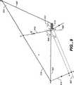
レンズ体314の傾斜角は任意の値に決められる(図8参照)。同図において、光線410、412は撮像面のエッジ414およびその反対側の撮像面エッジ416でそれぞれ散乱する。レンズ面307は、レンズの厚さがゼロに近づいたときの理論上のレンズ体314である。距離Aaはプリズム310内に現れる物体の見かけ像からレンズ面307までの光線410に沿った距離であり、距離B’bはプリズム310内に現れる物体の見かけの像からの光線412に沿った距離である。台形歪みを略ゼロにするためには、距離Aaが距離B’bに実質上等しくなければならない。B’bはプリズム310内に現れる物体の見かけの奥行きなので、従来の技術で述べたように次式が成り立つ。
【0051】
B’b=Bb/n
ここで、Bbはエッジ416上の点Bからプリズム310表面の点bまでの距離である。台形歪みを実質上ゼロにし、全体的な像の鮮明さを高めるための条件は以下の式で表わされる。
【0052】
Aa=Bb/n (式1)
光線412が出射面320に入射する角度、つまり、出射面320の法線とプリズム310内部の光線412との角度を図8ではθ1として表し、光線412がプリズム310を通って出射する際に屈折する角度はθ2で表すと、スネルの法則によって次式が成り立つ。
【0053】
n=sinθ2/sinθ1 (式2)
また、三角関数の基本定理を用いると次式が成立することがわかる。
【0054】
ABcosγ+Bbcosα’=Ab (式3)
ここで、ABは点Aから点Bまでのプリズム310の撮像面の長さであり、Abは出射面320上の線分Abの長さであり、α’は光線412と出射面320との間の角度であって、90°−θ1に等しい。また、γは撮像面318と出射面320とがなす角度で、図8では角度342として示されている。
【0055】
最後に、正弦法則を用いると次式が成立することがわかる。
【0056】
AB/Bb=cosθ1/sinγ (式4)
上記の式1、2、3、および4を用いると、台形歪みを実質的にゼロにし、さらに全体的な像の鮮明さを上げるためには、次式に示す、プリズム310の角度、およびレンズ面307と出射面320との角度に関する条件が満たされなければならない。
【0057】
(n2−sin2δ)1/2(cotγ)(sinδ)+sin2δ=1 (式5)
ここで、図8に示すように、δはレンズ体314のレンズ面307が出射面320に対してなす角度である。よって、本発明の撮像システム308は、台形歪みを略ゼロにし、全体的な像の鮮明さを上げるためには、式5に基づいて構成するのが好ましい。
【0058】
ただし、撮像システム308を製造する際に角度γと角度δについて正確な公差を達成するのは難しく、またコストが高くなる。よって、本発明の撮像システムに対して、30%の製造公差を許容することにより、以下に示す式6に基づいて構成することが好ましい。
【0059】
0.7≦(n2−sin2δ)1/2(cotγ)(sinδ)+sin2δ≦1.3 (式6)
さらに好ましくは、本発明の撮像システムの製造公差を15%まで許容し、以下に示す式7にしたがって構成するとよい。
【0060】
0.85≦(n2−sin2δ)1/2(cotγ)(sinδ)+sin2δ≦1.15 (式7)
また、本発明の撮像システムの製造公差を7.5%まで許容し、本発明の撮像システムを以下に示す式8にしたがって構成することが最も好ましい。
【0061】
0.925≦(n2−sin2δ)1/2(cotγ)(sinδ)+sin2δ≦1.075 (式8)
上述のように、撮像システム308を上記の式5〜8のうちの一つの式に基づいて構成することにより、台形歪みを大幅に、あるいはゼロにまで抑えられ、全体的な像の鮮明さを上げることができる。これにより、撮像システムが像を処理、比較する精度を容易に上げることができるという利点がある。
【0062】
プリズム310はガラスやアクリルなど、屈折率が1(空気の屈折率)より大きい透明な材料を用いて作製することができる。好ましい屈折率と角度とを備えたプリズムは、LAK−7およびLAK−8と命名されたガラス製の製品が韓国ソウルのシンクワン社(Shinkwang Ltd.)から入手可能である。
【0063】
レンズ体314などのレンズ体については、韓国ソウルのウーリム光学システム社(Woorim Optical System Ltd.)のガラス製品(商品名BK7)が好ましい。図6に示すように、レンズ体314が複数の構成要素で構成されているのであれば、それぞれの構成要素をプラスチック成形など既知の加工手段を用いて加工した枠の中に収めることで、構成要素を配置し間隔を決定することができる。
【0064】
光源312は回路基板上でまっすぐなアレー状に配置した4つの標準LEDで構成されるのが好ましい。LEDの駆動については当業者であれば周知である。イメージセンサ316は好ましくはCMOS型センサであり、韓国ソウルの現代電子社(Hyundai Electronics)、カリフォルニア・サンホセのVLSIビジョン社、カリフォルニア・サニーヴェールのオムニビジョン・テクノロジーズ社(Omnivision Technologies Inc.)から入手可能である。
【0065】
図4で示すように、撮像用部品を相対的な位置に固定するために、個々の部品を保持するためのスロットを備えた枠をプラスチック成形するなどして組み立ててもよい。光源312は出射面320に近接した保持スロットに配置するか、あるいは従来から知られているように、接着剤を用いて出射面320に直接取り付けてもよい。
【0066】
式5〜8は、撮像面318の全幅ABを利用して撮像を行うことを前提として導いたが、プリズムの撮像面全体を使わなくても撮像は可能である。一例として、角度が90°以上の三角プリズムを光屈折器として用いた場合が挙げられる。ただし、プリズムの撮像面全体を対象物の撮像に用いないのであれば、上記式5〜8に基づいて構成するという条件に加えて、その撮像システムの構成が別のもう一つの条件を満たすことが好ましい。このもう一つの条件を説明する。図9は角度541が鈍角である三角プリズム510を示している。三角プリズム510は平坦な撮像面518、平坦な出射面520、および平坦なもう一つの面522を有している。図9はさらに光源312と実質的に同じ光源512と、図示しないレンズ体のレンズ面507とを示している。プリズム510とともに使用するレンズ体はレンズ体314と略同じである。
【0067】
図9に示すように、光線612は撮像面538上の点Dで散乱し、光線610は撮像面518から点Aで散乱する。プリズム510とレンズ面507とは式5にしたがって構成されている。さらに、線分a’d’はレンズ面507に対して平行であり、長さD’d’は物体の像がプリズム510内で撮像面518上の点Dでの見かけの奥行きである。このように、線分Aa’およびD’d’の長さは等しい。プリズム510の屈折率は1より大きいので、光線612はプリズム510から点d’で出射する際に屈折してしまい、出射面520の法線620からずれた方向に進む。
【0068】
光線612と出射面520とがなす、出射面と撮像面との交差部の側に位置する角度545(図9ではα’と表記)は90°未満である。したがって、光線612がプリズム510を通過して法線620からずれた方向へ屈折すると、プリズム510外部の光線610に平行な光路を進む。つまり、線分aa’とd’dとが等しい。したがって、撮像面518上の物体について、プリズム510内に現れる見かけの像からレンズ面507、さらに最終的には、図示しないイメージセンサに到る光路が点Aでも点Dでも等しいことになる。これにより、全体的な像の鮮明さを上げることができる。
【0069】
次に、同じくプリズム510を示す図10を参照して説明する。プリズム510内に現れる、撮像面518上の点Eに置いた物体の見かけの像からの光路長と、プリズム510内に現れる、プリズム510上の点Aに置いた物体の見かけの像からの光路長とは等しくない。光線612は撮像面518上に置かれた物体からの散乱光である。上記のように、プリズム510の屈折率は1より大きいので、光線612は、点e’でプリズム510から出射する際に屈折し、出射面520の法線620からずれた方向へ屈折する。つまり、α’と表記した角度545は90°より大きいので、プリズム510外部における光線612の光路は、プリズム510外部における光線610の光路と平行ではない。光線610と光線612とが平行ではないのであるから、線分e’eの長さが線分a’aの長さとは異なることになる。つまり、プリズム510内の見かけの像からレンズ面507までに到る総光路長は、対象物が撮像面318上の点Eにある場合と同面上の点Aにある場合とでは異なることになる。そのため、比較的大きな台形歪みの発生及び/又は比較的ピントのぼけた像が形成される。
【0070】
上記のような像が形成されるのを避けるには、前述のように、角度が90°以上のプリズムを本発明の撮像システムにおいて使用する場合、撮像面をその幅の一部に限って使用して対象物を撮像するのが好ましい。上記のように、α’が90°未満で、撮像システムが上記式5〜8にしたがって構成されていれば、台形歪みは実質上なくなる。また、α’が90°以上であれば、台形歪みが発生する。したがって、撮像対象物をプリズムの撮像面518に当てる際に該撮像面518の一部にのみ当てようとするのであれば、少なくとも一本の光線と出射面520とが該出射面520の撮像面518との交差側から見て90°未満の角度(図9、10ではα’と表記)で交わるように、撮像に用いる撮像面518のどの部分も少なくとも一本の光線を散乱させることができなければならない。この基準を用いれば、上記式5〜8にしたがって構成された撮像システムにおいて台形歪みの発生を抑えたり、あるいは略一切発生しないようにしたりすることが容易にできるようになり、また、全体的な像の鮮明さを上げることができるという利点がある。
【0071】
プリズム510及び光源512は、プリズム310及び光源312について上述した材料及び方法によって同様に製造することができる。なお、POの撮像方法は、撮像面と、出射面と、さらにもう一つの面とを有する光屈折器を備えて行われる。出射面によって定められる平面と撮像面によって定められる平面との間には角度γが形成される。POは撮像面に対して置かれ、入射光は光屈折器に入射される。入射光は撮像面及びPOで散乱し、出射面を通過する。レンズは出射面に近接して配置され、レンズの焦点面と出射面によって定められる平面との間に角度δをなす。角度γおよび角度δは、光屈折器で形成された、POの見かけ像の一部からレンズ面までの第一光線の光路長であり、最終的にはイメージセンサまでの光路長と、第一光線に略平行で、POの見かけ像の別の部分から、レンズ面及びイメージセンサまでの別の光線の光路長とが実質的に等しくなるように設定される。
【0072】
本発明は、その精神と技術的範囲を逸脱しない範囲にて多種多様な実施形態が可能である。すなわち、本発明は明細書に開示した具体的な実施の形態に限定されない。例えば、上記本発明の実施の形態は指紋の撮像との関連で説明したが、これ以外にも任意のタイプのPOの撮像にも本発明は適用できる。
【図面の簡単な説明】
【図1】 吸収式撮像技術を用いた、従来の撮像装置の概略図である。
【図2】 図1の撮像装置の台形歪みを説明する概略図である。
【図3】 散乱式撮像技術を用いた第2の従来の撮像装置の概略図である。
【図4】 本発明に係る撮像装置の概略図であり、プリズム、光源、レンズ体、イメージセンサを示している。
【図5】 図4に示すプリズム及び光源の斜視図である。
【図6】 図4に示す撮像システムにて、台形の歪みを低減する方法を示す概略図である。
【図7】 図4に示す撮像システムにて使用されるレンズ体を示す概略図である。
【図8】 図4に示す撮像システムにて、プリズム及びレンズ体の好ましい構成を示す概略図である。
【図9】 本発明の撮像装置で使用可能な他の実施形態のプリズムの散乱光路を説明する概略図である。
【図10】 図9に示すプリズムの他の散乱光路を説明する概略図である。Field of Invention
The present invention relates to an optical imaging apparatus used in an image capture and recognition system, and in particular, reduces or substantially eliminates trapezoidal distortion of an image of a patterned object (hereinafter referred to as PO), The present invention relates to an optical imaging apparatus that makes the image clearer.
[0001]
Conventional technology
PO recognition systems are generalized industrially and commercially, and are used in various applications such as scanners for scanning documents, pictures and photographs. In recent years, manufacturers are trying to reduce costs in order to promote the use of pattern recognition systems for general consumers. One example of the use of such a pattern recognition system for consumer products is fingerprint imaging and recognition. This makes it possible to improve security by, for example, collecting a fingerprint of a computer user and comparing it with the fingerprint of a user who has the authority to use the computer or access a specific file / function. . Such a system can be an alternative to a security system, for example with a login name and password.
[0002]
First of all, such a fingerprint recognition system and other pattern recognition systems are required to accurately photograph fingerprints and other patterns for analysis. Various mechanisms have already been developed for obtaining pattern information. For example, US Pat. Nos. 3,975,711, 4,681,435, 5,051,576, 5,177,435, and 5 No. 233,404 discloses an apparatus for capturing PO images.
[0003]
FIG. 1 is a schematic view showing such a conventional optical fingerprint photographing recognition system. In FIG. 1, the
[0004]
In general,
[0005]
The
[0006]
The storage and
[0007]
When a fingerprint is placed on the
[0008]
As a result of scattering or absorption, the
[0009]
In the above system, it is possible to perform processing for optically capturing a fingerprint image and electrically expressing the fingerprint image. However, in the ridge 111 of the fingerprint, a part of the
[0010]
Further, in an optical recognition system such as the
[0011]
However, as shown in FIG. 2, in an absorptive system such as
[0012]
Therefore, as shown in FIG. 2, when the lens body of the
[0013]
Thus, as shown in FIG. 2, in the absorption system, in order to capture the entire fingerprint image with substantially parallel rays, the
[0014]
In addition, when the first lens of the
[0015]
FIG. 2 is a schematic diagram illustrating why trapezoidal distortion occurs in the
[0016]
aa '= Aa' / n
Here, n is the refractive index of the
[0017]
bb '= Bb' / n
In the trapezoidal distortion, the length of the optical path from the apparent image of the object to the
[0018]
Further, since the distance aA 'is longer than the distance bB', it is difficult to obtain an image of an object that is in focus at any part. In general, if the optical path length from the image of the apparent object to the lens surface of the lens body, and finally the optical path length to the image sensor, varies depending on the part of the object that forms the image, Some parts are in focus and some parts are blurred.
[0019]
In order to solve such a problem that the trapezoidal distortion and a part of the image of the object are blurred, in the related art, the
[0020]
Therefore, tilting the
[0021]
In addition, the stray light 113 from the
[0022]
In order to solve the problems of the absorption type imaging system as described above, an imaging system based on the “scattering type” instead of the absorption type has been devised. One example is disclosed in J. Lougheed et al., Aug. 3, 1993. U.S. Pat. No. 5,233,404. FIG. 3 is a schematic diagram showing the imaging unit of the apparatus by Lougheed et al. As shown in FIG. 3, the conventional imaging system 208 includes a
[0023]
The imaging surface 218 is a surface on which an object to be imaged such as a fingerprint is placed. The
[0024]
In the region of the
[0025]
As shown in FIG. 1, the difference in the intensity of light between the ridges and valleys of the fingerprint image formed by the scattering system, or the degree of intensity, is as follows. It is larger than the difference in intensity of light or the degree of intensity. This makes the contrast between the ridges and valleys of the fingerprint image formed by the scattering system clearer than that by the absorption system. In this way, the
[0026]
Further, due to the characteristics of the scattering system, a clear image is formed even if the light rays entering the
[0027]
However, a trapezoidal prism such as
[0028]
Further, since the optical path length of the scattered light from the apparent image of the fingerprint on the
[0029]
As is apparent from the above description, there is a demand for improvement of the imaging apparatus for the PO recognition system. Specifically, an imaging apparatus that reduces or substantially eliminates the trapezoidal distortion of an image is desired. Furthermore, it is desirable that the imaging device be focused on almost all parts of the image, and it is preferable that the imaging device be relatively compact and inexpensive to manufacture.
[0030]
Summary of the Invention
The present invention includes an imaging device that forms a high-contrast, low-distortion image with reduced or substantially eliminated trapezoidal distortion. Furthermore, the imaging system of the present invention can be manufactured at a relatively low price. The imaging apparatus includes an optical refractor including an imaging surface on which an object is arranged, another surface, and an exit surface in order to form an apparent image of PO. The exit surface is close to the imaging surface and forms an angle γ with the imaging surface. The PO image is projected from the exit surface. The imaging device also includes a lens close to the exit surface for receiving the PO image and focusing. The lens has a lens surface that is perpendicular to the optical axis and forms an angle δ with respect to the exit surface. Angle γ and angle δ are the optical path length of the first light beam from a part of the apparent image of PO to the lens surface, and finally the optical path length to the image sensor and the apparent image of PO substantially parallel to the first light beam. Is an optical path length of another light beam from another portion of the lens to the lens surface, and finally an angle made to make the optical path length to the image sensor substantially equal. Preferably, the angle γ and the angle δ may be set so that the following expression is satisfied.
[0031]
0.7 ≦ (n2−sin2(δ)1/2(cotγ) (sinδ) + sin2δ ≦ 1.30
The present invention also provides that the exit surface and the light beam form an angle of less than 90 ° on the side of the intersection of the exit surface and the imaging surface, and any part of the imaging surface on which the object to be imaged is placed, It is preferable to have a configuration in which at least one light beam is scattered.
[0032]
The present inventionIs a manufacturing method of the above-described small-sized device, and includes a step of forming a light refractor (310), a plane defined by an exit surface (320), and a plane defined by an imaging surface (318). Forming a non-zero angle γ (342), a light source (312), a first light shielding part (350), a second light shielding part (352), and the lens surface Placing a lens (314) proximate to the exit surface so as to be perpendicular to the optical axis of the system passing through the center of the lens, and between the plane defined by the exit surface and the lens surface Forming a non-zero angle δ (343), an optical path length of the first light beam from a part of the apparent image to the lens surface, and substantially parallel to the first light beam, the apparent image From another part of And setting the angle γ and the angle δ so that the optical path lengths of the other light beams to the lens surface are substantially equal.Preferably, the angle γ and the angle δ are set so that the following relationship is established.
[0033]
0.7 ≦ (n2−sin2(δ)1/2(cotγ) (sinδ) + sin2δ ≦ 1.30
Furthermore, when the intersection of the light beam and the exit surface is viewed from the intersection of the exit surface and the imaging surface, a first angle of less than 90 ° is formed, and any part of the imaging surface used for imaging is at least It is preferable to have a configuration in which one light beam is scattered.
[0034]
With the above-described apparatus and method, it is possible to image PO with little or no trapezoidal distortion and form an image with a relatively clear focus. This makes it possible to effectively promote more accurate processing and comparison of PO.
[0035]
Detailed Description of the Invention
4 and 5 show a system 308 for projecting an image of an object (patterned object, hereinafter referred to as PO) on which a pattern according to the present invention is formed. The imaging system 308 preferably includes a
[0036]
The
[0037]
The
[0038]
The
[0039]
In order to form an image of the
[0040]
Since the
[0041]
Since the
[0042]
In addition to the above-described configuration, the imaging system 308 is preferably provided with a light-shielding
[0043]
Since the
[0044]
By minimizing the incident light 324 that is directly incident on the imaging surface from the
[0045]
Furthermore, this scattering technique for imaging is realized using a triangular prism as opposed to the trapezoidal prism disclosed by Lougheed, as described in the prior art. Triangular prisms have higher production efficiency than trapezoidal prisms, and imaging system 308 has the advantage of relatively low manufacturing costs.
[0046]
In general, scattered light does not scatter in one direction from an object, but scatters in many directions. As described in the prior art, if a lens body is used, an image of an in-focus object can be formed with non-parallel scattered light. That is, as shown in the
[0047]
As shown in FIG. 6, since the diameter of the first lens of the
[0048]
However, unlike the
[0049]
However, the refractive index of the
[0050]
The inclination angle of the
[0051]
B'b = Bb / n
Here, Bb is the distance from the point B on the
[0052]
Aa = Bb / n (Formula 1)
The angle at which the
[0053]
n = sin θ2/ Sinθ1 (Formula 2)
It can also be seen that the following equation holds when using the basic theorem of trigonometric functions.
[0054]
ABcos γ + Bbcos α ′ = Ab (Formula 3)
Here, AB is the length of the imaging surface of the
[0055]
Finally, it can be seen that the following equation holds when the sine law is used.
[0056]
AB / Bb = cos θ1/ Sinγ (Formula 4)
Using
[0057]
(n2−sin2(δ)1/2(cotγ) (sinδ) + sin2δ = 1 (Formula 5)
Here, as shown in FIG. 8, δ is an angle formed by the
[0058]
However, it is difficult to achieve an accurate tolerance for the angle γ and the angle δ when manufacturing the imaging system 308, and the cost increases. Therefore, it is preferable that the imaging system according to the present invention is configured based on Expression 6 shown below by allowing a manufacturing tolerance of 30%.
[0059]
0.7 ≦ (n2−sin2(δ)1/2(cotγ) (sinδ) + sin2δ ≦ 1.3 (Formula 6)
More preferably, the manufacturing tolerance of the imaging system of the present invention is allowed up to 15%, and it is configured according to
[0060]
0.85 ≦ (n2−sin2(δ)1/2(cotγ) (sinδ) + sin2δ ≦ 1.15 (Formula 7)
In addition, it is most preferable that the manufacturing tolerance of the imaging system of the present invention is allowed up to 7.5%, and the imaging system of the present invention is configured according to Equation 8 shown below.
[0061]
0.925 ≦ (n2−sin2(δ)1/2(cotγ) (sinδ) + sin2δ ≦ 1.075 (Formula 8)
As described above, when the imaging system 308 is configured based on one of the above equations 5 to 8, the trapezoidal distortion can be greatly suppressed to zero, and the overall image sharpness can be reduced. Can be raised. Accordingly, there is an advantage that the accuracy with which the imaging system processes and compares images can be easily increased.
[0062]
The
[0063]
For the lens body such as the
[0064]
The
[0065]
As shown in FIG. 4, in order to fix the imaging components at relative positions, a frame having slots for holding the individual components may be assembled by plastic molding or the like. The
[0066]
Equations 5 to 8 are derived on the assumption that imaging is performed using the full width AB of the
[0067]
As shown in FIG. 9, the
[0068]
An angle 545 (denoted by α ′ in FIG. 9) located on the side of the intersection between the exit surface and the imaging surface formed by the
[0069]
Next, description will be made with reference to FIG. The optical path length from the apparent image of the object placed at point E on the
[0070]
In order to avoid the formation of the image as described above, as described above, when a prism having an angle of 90 ° or more is used in the imaging system of the present invention, the imaging surface is limited to a part of its width. The object is preferably imaged. As described above, when α ′ is less than 90 ° and the imaging system is configured according to the above formulas 5 to 8, trapezoidal distortion is substantially eliminated. If α ′ is 90 ° or more, trapezoidal distortion occurs. Therefore, when the imaging object is applied to the
[0071]
[0072]
Various embodiments of the present invention are possible without departing from the spirit and technical scope of the present invention. That is, the present invention is not limited to the specific embodiments disclosed in the specification. For example, the above embodiment of the present invention has been described in relation to fingerprint imaging, but the present invention can also be applied to imaging of any type of PO other than this.
[Brief description of the drawings]
FIG. 1 is a schematic diagram of a conventional imaging apparatus using an absorption imaging technique.
FIG. 2 is a schematic diagram for explaining trapezoidal distortion of the image pickup apparatus in FIG. 1;
FIG. 3 is a schematic diagram of a second conventional imaging device using a scattering imaging technique.
FIG. 4 is a schematic diagram of an imaging apparatus according to the present invention, showing a prism, a light source, a lens body, and an image sensor.
5 is a perspective view of a prism and a light source shown in FIG.
6 is a schematic diagram showing a method of reducing trapezoidal distortion in the imaging system shown in FIG.
7 is a schematic view showing a lens body used in the imaging system shown in FIG.
8 is a schematic diagram showing a preferable configuration of a prism and a lens body in the imaging system shown in FIG.
FIG. 9 is a schematic diagram illustrating a scattered light path of a prism according to another embodiment that can be used in the imaging apparatus of the present invention.
10 is a schematic diagram illustrating another scattered light path of the prism shown in FIG.
Claims (5)
Translated fromJapanese長さを持つ対象物(335)を配置する平坦な矩形の撮像面(318)と、
前記撮像面に隣接する面であって前記対象物の像が出射され、前記撮像面(318)に対してゼロにならない角度γ(342)をなし、その一部が光を入射する受光面としての役割も果たす、平坦な矩形の出射面(320)と、
照射される入射光のうち光屈折器(310)の内部で散乱する割合を高くするとともに、入射光を前記撮像面(318)に均一に照射させるために、入射光を反射および拡散させる、前記出射面(320)に対してゼロにならない角度(341)をなすさらにもう一つの面(322)と、
前記撮像面(318)に対向し、前記出射面(320)に隣接する第一稜線(338)とを含み、
光を反射および屈折させ、屈折率nがn>1であり、5面体の三角プリズム(310)である、光屈折器(310)と、
前記光屈折器(310)に隣接して設けられ、前記出射面(320)にて前記対象物の像を形成するために、前記光屈折器(310)に入射する入射光を出射するための、少なくとも一つの光源(312)と、
前記出射面(320)の一部に配され、前記光屈折器(310)の内側に対向している鏡面を有することにより、レンズ(314)に入射し、前記対象物の像に干渉してぼやけさせてしまう、前記光源(312)からの迷い光の量を低減する第1の遮光部(350)と、
前記光源(312)からの迷い光を遮断してレンズ(314)に入射させない角度で前記出射面(320)から延びている第2の遮光部(352)と、
前記光屈折器(310)の外側にあり、前記出射面(320)に近接して、当該出射面(320)から前記光屈折器(310)を通過して出射される光を受け取るとともに、前記対象物の像を形成するための前記光の焦点をあわせる少なくとも一つのレンズ(314)とを含み、
前記レンズ(314)は、レンズ(314)の中心を通るシステムの光軸に対して垂直であって、前記出射面(320)に対してゼロにならない角度δ(343)をなすレンズ面を有し、撮像される前記対象物の長さよりも小さい直径を有しており、
前記光源は、前記出射面(320)に向けられ、前記出射面(320)に平行であるとともに、前記第一稜線(338)に隣接する発光ダイオード(LED)の列であり、
前記角度γおよび角度δは、見かけ像の一部から前記レンズ面までの第一光線の光路長と、当該第一光線に実質的に平行であり、前記見かけ像の別の部分から前記レンズ面までの別の光線の光路長とが実質的に等しくなるように形成されている小型装置。A small device that forms a high-contrast, low-distortion image of an object with a pattern, such as a fingerprint,
A flat rectangular imaging surface (318) for placing an object (335) having a length;
As a light-receiving surface that is adjacent to the imaging surface and has an angle γ (342) that does not become zero with respect to the imaging surface (318), an image of the object is emitted, and a part of which is incident on the light A flat rectangular exit surface (320) that also serves as:
The incident light is reflected and diffused in order to increase the proportion of the incident light scattered inside the photorefractive element (310) and to uniformly irradiate the imaging surface (318) with the incident light. Yet another surface (322) forming a non-zero angle (341) with respect to the exit surface (320);
A first ridge line (338) facing the imaging surface (318) and adjacent to the exit surface (320);
An optical refractor (310) that reflects and refracts light, the refractive index n is n> 1, and is a pentahedral triangular prism (310);
Provided adjacent to the light refractor (310) and for emitting incident light incident on the light refractor (310) to form an image of the object on the exit surface (320). At least one light source (312);
By having a mirror surface disposed on a part of the exit surface (320) and facing the inner side of the photorefractive device (310), it enters the lens (314) and interferes with the image of the object. A first light-blocking portion (350) that reduces the amount of stray light from the light source (312) that blurs,
A second light shielding portion (352) extending from the exit surface (320) at an angle that blocks stray light from the light source (312) and does not enter the lens (314);
Receiving light emitted from the exit surface (320) through the light refractor (310), outside the light refractor (310), in proximity to the exit surface (320), and At least one lens (314) for focusing the light to form an image of the object;
The lens (314) has a lens surface that is perpendicular to the optical axis of the system passing through the center of the lens (314) and forms an angle δ (343) that is not zero with respect to the exit surface (320). And having a diameter smaller than the length of the object to be imaged,
The light source is a row of light emitting diodes (LEDs) that are directed to the exit surface (320), parallel to the exit surface (320), and adjacent to the first ridge line (338);
The angle γ and the angle δ are substantially parallel to the optical path length of the first light beam from a part of the apparent image to the lens surface, and from the other part of the apparent image to the lens surface. A small device that is formed so that the optical path length of another light beam is substantially equal.
0.7≦(n2−sin2δ)1/2(cotγ)(sinδ)+sin2δ≦1.3
が成り立つ、請求項1記載の小型装置。In the relationship between the angle γ and the angle δ,
0.7 ≦ (n2 −sin2 δ)1/2 (cot γ) (sin δ) + sin2 δ ≦ 1.3
The small device according to claim 1, wherein:
0.85≦(n2−sin2δ)1/2(cotγ)(sinδ)+sin2δ≦1.15
が成り立つ、請求項1記載の小型装置。In the relationship between the angle γ and the angle δ,
0.85 ≦ (n2 −sin2 δ)1/2 (cot γ) (sin δ) + sin2 δ ≦ 1.15
The small device according to claim 1, wherein:
0.925≦(n2−sin2δ)1/2(cotγ)(sinδ)+sin2δ≦1.075
が成り立つ、請求項1記載の小型装置。In the relationship between the angle γ and the angle δ,
0.925 ≦ (n2 −sin2 δ)1/2 (cot γ) (sin δ) + sin2 δ ≦ 1.075
The small device according to claim 1, wherein:
Applications Claiming Priority (3)
| Application Number | Priority Date | Filing Date | Title |
|---|---|---|---|
| US09/368,442US6324020B1 (en) | 1999-08-04 | 1999-08-04 | Method and apparatus for reduction of trapezoidal distortion and improvement of image sharpness in an optical image capturing system |
| US09/368,442 | 1999-08-04 | ||
| PCT/US2000/040530WO2001011549A2 (en) | 1999-08-04 | 2000-08-01 | Method and apparatus for reduction of trapezoidal distortion and improvement of image sharpness in an optical image capturing system |
Publications (2)
| Publication Number | Publication Date |
|---|---|
| JP2003506798A JP2003506798A (en) | 2003-02-18 |
| JP3877058B2true JP3877058B2 (en) | 2007-02-07 |
Family
ID=23451225
Family Applications (1)
| Application Number | Title | Priority Date | Filing Date |
|---|---|---|---|
| JP2001516128AExpired - Fee RelatedJP3877058B2 (en) | 1999-08-04 | 2000-08-01 | Small apparatus and manufacturing method thereof |
Country Status (11)
| Country | Link |
|---|---|
| US (1) | US6324020B1 (en) |
| EP (1) | EP1210686B1 (en) |
| JP (1) | JP3877058B2 (en) |
| KR (1) | KR100469571B1 (en) |
| CN (1) | CN1178154C (en) |
| AT (1) | ATE306697T1 (en) |
| AU (1) | AU7389700A (en) |
| CA (1) | CA2381300C (en) |
| DE (1) | DE60023156T2 (en) |
| TW (1) | TW521214B (en) |
| WO (1) | WO2001011549A2 (en) |
Families Citing this family (30)
| Publication number | Priority date | Publication date | Assignee | Title |
|---|---|---|---|---|
| US6870946B1 (en) | 1998-08-06 | 2005-03-22 | Secugen Corporation | Compact optical fingerprint capturing and recognition system |
| US6381347B1 (en) | 1998-11-12 | 2002-04-30 | Secugen | High contrast, low distortion optical acquistion system for image capturing |
| KR100353731B1 (en) | 2000-11-01 | 2002-09-28 | (주)니트 젠 | User authenticating system and method using one-time fingerprint template |
| US20030105966A1 (en)* | 2001-05-02 | 2003-06-05 | Eric Pu | Authentication server using multiple metrics for identity verification |
| KR100451541B1 (en)* | 2001-07-10 | 2004-10-08 | (주)니트 젠 | Method of providing user interface via web |
| KR100432490B1 (en) | 2001-09-17 | 2004-05-22 | (주)니트 젠 | Optical fingerprint acquisition apparatus |
| DE10163351C1 (en)* | 2001-12-14 | 2003-06-26 | Heimann Biometric Systems Gmbh | Method and arrangement for the low-distortion recording of intensity patterns created on a contact surface by disturbed total reflection |
| US7088872B1 (en) | 2002-02-14 | 2006-08-08 | Cogent Systems, Inc. | Method and apparatus for two dimensional image processing |
| KR20040039856A (en)* | 2002-11-05 | 2004-05-12 | 주식회사 코렌 | Apparatus for recognizing information of live body |
| US7050158B2 (en)* | 2002-12-24 | 2006-05-23 | Guolin Ma | Compact image pickup module |
| US7426020B2 (en)* | 2003-06-17 | 2008-09-16 | Cross Match Technologies, Inc. | System for print imaging with prism illumination optics |
| US6954261B2 (en)* | 2003-06-17 | 2005-10-11 | Cross Match Technologies, Inc. | System and method for illuminating a platen in a live scanner and producing high-contrast print images |
| FR2861200B1 (en)* | 2003-10-17 | 2006-01-20 | Sagem | OPTICAL DEVICE FOR FORMING AN IMAGE OF DIGITAL IMPRESSIONS |
| US7509658B2 (en) | 2004-01-30 | 2009-03-24 | Research In Motion Limited | System and method for adaptable provisioning of generic application content |
| EP1560115A1 (en)* | 2004-02-02 | 2005-08-03 | Research In Motion Limited | Computer system and method for adaptable provisioning of generic application content |
| US7616788B2 (en)* | 2004-11-12 | 2009-11-10 | Cogent Systems, Inc. | System and method for fast biometric pattern matching |
| US8131477B2 (en) | 2005-11-16 | 2012-03-06 | 3M Cogent, Inc. | Method and device for image-based biological data quantification |
| WO2007059694A1 (en)* | 2005-11-24 | 2007-05-31 | Zksoftware Inc. | Large area fingerprint recognition device |
| US8275179B2 (en) | 2007-05-01 | 2012-09-25 | 3M Cogent, Inc. | Apparatus for capturing a high quality image of a moist finger |
| US7834988B2 (en)* | 2007-05-31 | 2010-11-16 | Ramendra Deo Bahuguna | Fingerprint sensor using a spectral filter and a holographic optical element |
| US8411916B2 (en)* | 2007-06-11 | 2013-04-02 | 3M Cogent, Inc. | Bio-reader device with ticket identification |
| US9342729B2 (en) | 2010-08-06 | 2016-05-17 | Secugen Corporation | Fake fingerprint detection system |
| JP5633054B2 (en)* | 2010-10-29 | 2014-12-03 | 株式会社オプトロジック | Imaging device |
| JP5748201B2 (en)* | 2011-01-27 | 2015-07-15 | Necエンジニアリング株式会社 | Image reading device |
| KR101298123B1 (en)* | 2012-06-04 | 2013-08-20 | 주식회사 유니온커뮤니티 | Optical fingerprint acquisition apparatus |
| CN105022983A (en)* | 2014-04-30 | 2015-11-04 | 聚晶半导体股份有限公司 | Image identification system using multi-lens assistance and method thereof |
| RU2597465C2 (en)* | 2015-01-23 | 2016-09-10 | Антон Сергеевич Прытков | Compact papillary picture recording system |
| CN107515435B (en)* | 2017-09-11 | 2020-12-29 | 京东方科技集团股份有限公司 | Display panels and display devices |
| CN108470366B (en)* | 2018-03-28 | 2020-10-16 | 同方威视技术股份有限公司 | Simulation image generation method and apparatus and computer readable storage medium |
| CN211741813U (en)* | 2020-03-12 | 2020-10-23 | 中强光电股份有限公司 | Optical element and projection device using the same |
Family Cites Families (58)
| Publication number | Priority date | Publication date | Assignee | Title |
|---|---|---|---|---|
| US3527535A (en)* | 1968-11-15 | 1970-09-08 | Eg & G Inc | Fingerprint observation and recording apparatus |
| US3864042A (en)* | 1973-05-10 | 1975-02-04 | Stephen Richard Leventhal | Fingerprint scanning system |
| US3975711A (en) | 1974-08-30 | 1976-08-17 | Sperry Rand Corporation | Real time fingerprint recording terminal |
| US4210899A (en) | 1975-06-23 | 1980-07-01 | Fingermatrix, Inc. | Fingerprint-based access control and identification apparatus |
| US4135147A (en) | 1976-09-10 | 1979-01-16 | Rockwell International Corporation | Minutiae pattern matcher |
| US4120585A (en) | 1976-11-19 | 1978-10-17 | Calspan Corporation | Fingerprint identification system using a pliable optical prism |
| DE3072034D1 (en) | 1979-12-24 | 1987-10-29 | Electro Optic Dev | Method and device for carrying out a comparison between certain patterns, especially finger prints |
| US4340300A (en) | 1980-08-11 | 1982-07-20 | Siemens Corporation | Input sensor unit for a fingerprint identification system |
| US4832485A (en) | 1982-09-03 | 1989-05-23 | Commonwealth Technology, Inc. | Image enhancer |
| JPS59153514U (en) | 1983-03-31 | 1984-10-15 | 株式会社東海理化電機製作所 | Contact pattern observation device |
| DE3577485D1 (en) | 1984-07-18 | 1990-06-07 | Nec Corp | IMAGE INPUT DEVICE FOR PROCESSING A FINGERPRINT BEFORE IDENTIFICATION. |
| JPS61145686A (en)* | 1984-12-19 | 1986-07-03 | Mitsubishi Electric Corp | Fingerprint image identification system |
| JPS61221883A (en)* | 1985-03-25 | 1986-10-02 | Fujitsu Ltd | Personal verification device |
| JPS6274177A (en)* | 1985-09-27 | 1987-04-04 | Fujitsu Ltd | Uneven surface information detection method |
| US4668995A (en)* | 1985-04-12 | 1987-05-26 | International Business Machines Corporation | System for reproducing mixed images |
| JPH01145785A (en) | 1987-08-21 | 1989-06-07 | Nec Corp | Method and instrument for measuring surface shape |
| EP0308162A3 (en) | 1987-09-15 | 1990-06-06 | Identix Incorporated | Optical system for fingerprint imaging |
| US5222153A (en) | 1988-09-02 | 1993-06-22 | Thumbscan, Inc. | Apparatus for matching a fingerprint using a tacky finger platen |
| JP2773750B2 (en)* | 1988-11-15 | 1998-07-09 | 富士通株式会社 | Fingerprint image input device |
| JP2712469B2 (en)* | 1989-01-17 | 1998-02-10 | 富士通株式会社 | Fingerprint image input device |
| US4983415A (en) | 1989-07-21 | 1991-01-08 | Identicator Corporation | Method of making permanent images on recording surface having a thermosensitive color-developing layer thereon |
| JPH0395693A (en)* | 1989-09-08 | 1991-04-22 | Toshiba Corp | Finger picture input device |
| CA1286032C (en) | 1989-09-28 | 1991-07-09 | James H. Lougheed | Optical scanning and recording apparatus for fingerprints |
| JPH03246693A (en)* | 1990-02-26 | 1991-11-05 | Toshiba Corp | Input device for finger print information |
| US5177802A (en) | 1990-03-07 | 1993-01-05 | Sharp Kabushiki Kaisha | Fingerprint input apparatus |
| JPH03292578A (en)* | 1990-04-11 | 1991-12-24 | Nippondenso Co Ltd | Fingerprint reading device |
| KR920007329B1 (en)* | 1990-05-30 | 1992-08-31 | 금성사 주식회사 | Optical apparatus for finger printers recognition |
| US5051576A (en) | 1990-07-31 | 1991-09-24 | Michael Schiller | Finger surface image enhancement having a liquid layer on the finger touching surface of the platen |
| JP2547022Y2 (en) | 1990-10-12 | 1997-09-03 | 株式会社アドバンテスト | IC test equipment |
| KR930001001Y1 (en) | 1990-11-17 | 1993-03-02 | 주식회사 금성사 | Fingerprint recognition apparatus |
| JPH05216981A (en) | 1992-02-05 | 1993-08-27 | Nippon Oputoronikusu Kk | Fingerprint detector |
| JP2845048B2 (en) | 1992-09-04 | 1999-01-13 | 三菱自動車工業株式会社 | Engine cooling system with cylinder deactivation mechanism |
| JPH06282636A (en) | 1993-03-30 | 1994-10-07 | Nec Corp | Surface shape picture image pickup device |
| DE4421243A1 (en)* | 1993-06-21 | 1994-12-22 | Asahi Optical Co Ltd | Device for inputting a fingerprint |
| US5416573A (en) | 1993-09-10 | 1995-05-16 | Indentix Incorporated | Apparatus for producing fingerprint images which are substantially free of artifacts attributable to moisture on the finger being imaged |
| JPH07131322A (en) | 1993-10-28 | 1995-05-19 | Tec Corp | Touch changeover switch circuit |
| US5732148A (en) | 1994-09-16 | 1998-03-24 | Keagy; John Martin | Apparatus and method for electronically acquiring fingerprint images with low cost removable platen and separate imaging device |
| JP2937046B2 (en) | 1994-12-26 | 1999-08-23 | 日本電気株式会社 | Fingerprint image input device |
| US5812252A (en)* | 1995-01-31 | 1998-09-22 | Arete Associates | Fingerprint--Acquisition apparatus for access control; personal weapon and other systems controlled thereby |
| US5548394A (en) | 1995-03-16 | 1996-08-20 | Printrak International Inc. | Scanning fingerprint reading |
| DE19509751A1 (en) | 1995-03-17 | 1996-09-19 | Hans J Dr Einighammer | Optical imaging system for representing papillary ridge pattern |
| US5822445A (en) | 1995-06-27 | 1998-10-13 | Dew Engineering And Development Limited | Apparatus for identifying fingerprints |
| US5740276A (en) | 1995-07-27 | 1998-04-14 | Mytec Technologies Inc. | Holographic method for encrypting and decrypting information using a fingerprint |
| HU214533B (en) | 1995-10-06 | 1998-03-30 | Dermo Corporation Ltd. | Detector for identifying living character of a finger |
| US5796858A (en)* | 1996-05-10 | 1998-08-18 | Digital Persona, Inc. | Fingerprint sensing system using a sheet prism |
| US5875025A (en)* | 1996-07-15 | 1999-02-23 | Hamamatsu Photonics K.K. | Image input apparatus |
| US5680205A (en) | 1996-08-16 | 1997-10-21 | Dew Engineering And Development Ltd. | Fingerprint imaging apparatus with auxiliary lens |
| US5737071A (en) | 1996-08-16 | 1998-04-07 | Identicator Corporation | Method and apparatus for enhancing live-scan fingerprint reader images |
| US5963657A (en)* | 1996-09-09 | 1999-10-05 | Arete Associates | Economical skin-pattern-acquisition and analysis apparatus for access control; systems controlled thereby |
| WO1998011750A2 (en) | 1996-09-11 | 1998-03-19 | Yang Li | Method of using fingerprints to authenticate wireless communications |
| AU4341597A (en) | 1996-09-11 | 1998-04-02 | Yang Li | Embeddable module for fingerprint capture and matching |
| US6035403A (en) | 1996-09-11 | 2000-03-07 | Hush, Inc. | Biometric based method for software distribution |
| JPH11102432A (en) | 1997-09-26 | 1999-04-13 | Yamatake Corp | Fingerprint input device |
| US6185319B1 (en) | 1996-12-06 | 2001-02-06 | Yamatake Honeywell Co., Ltd. | Fingerprint input apparatus |
| WO1998035118A1 (en) | 1997-02-06 | 1998-08-13 | Siemens Aktiengesellschaft | Identification device |
| JP3011125B2 (en) | 1997-03-27 | 2000-02-21 | 日本電気株式会社 | Fingerprint detection device and method |
| JP3011126B2 (en) | 1997-03-27 | 2000-02-21 | 日本電気株式会社 | Fingerprint detection device |
| US6154285A (en)* | 1998-12-21 | 2000-11-28 | Secugen Corporation | Surface treatment for optical image capturing system |
- 1999
- 1999-08-04USUS09/368,442patent/US6324020B1/ennot_activeExpired - Lifetime
- 2000
- 2000-07-31TWTW089115343Apatent/TW521214B/ennot_activeIP Right Cessation
- 2000-08-01DEDE60023156Tpatent/DE60023156T2/ennot_activeExpired - Lifetime
- 2000-08-01CACA2381300Apatent/CA2381300C/ennot_activeExpired - Lifetime
- 2000-08-01AUAU73897/00Apatent/AU7389700A/ennot_activeAbandoned
- 2000-08-01KRKR10-2002-7001411Apatent/KR100469571B1/ennot_activeExpired - Fee Related
- 2000-08-01JPJP2001516128Apatent/JP3877058B2/ennot_activeExpired - Fee Related
- 2000-08-01ATAT00962029Tpatent/ATE306697T1/ennot_activeIP Right Cessation
- 2000-08-01WOPCT/US2000/040530patent/WO2001011549A2/enactiveIP Right Grant
- 2000-08-01CNCNB008112614Apatent/CN1178154C/ennot_activeExpired - Fee Related
- 2000-08-01EPEP00962029Apatent/EP1210686B1/ennot_activeExpired - Lifetime
Also Published As
| Publication number | Publication date |
|---|---|
| JP2003506798A (en) | 2003-02-18 |
| WO2001011549A3 (en) | 2001-08-16 |
| TW521214B (en) | 2003-02-21 |
| CN1178154C (en) | 2004-12-01 |
| DE60023156T2 (en) | 2006-06-29 |
| WO2001011549A2 (en) | 2001-02-15 |
| DE60023156D1 (en) | 2005-11-17 |
| AU7389700A (en) | 2001-03-05 |
| US6324020B1 (en) | 2001-11-27 |
| ATE306697T1 (en) | 2005-10-15 |
| CN1369077A (en) | 2002-09-11 |
| CA2381300C (en) | 2010-11-09 |
| WO2001011549A9 (en) | 2002-08-15 |
| EP1210686B1 (en) | 2005-10-12 |
| CA2381300A1 (en) | 2001-02-15 |
| EP1210686A2 (en) | 2002-06-05 |
| KR100469571B1 (en) | 2005-02-02 |
| KR20020033459A (en) | 2002-05-06 |
Similar Documents
| Publication | Publication Date | Title |
|---|---|---|
| JP3877058B2 (en) | Small apparatus and manufacturing method thereof | |
| TW511038B (en) | High contrast, low distortion optical acquisition systems for image capturing | |
| JP3897852B2 (en) | Medium surface shape data acquisition method | |
| US4428670A (en) | Fingerprint sensing device for deriving an electric signal | |
| US5146102A (en) | Fingerprint image input apparatus including a cylindrical lens | |
| KR100668361B1 (en) | Fingerprint Image Optical Input Device | |
| JPH07220041A (en) | Rough surface reading device | |
| CA2193041A1 (en) | Mouse adapted to scan biometric data | |
| JP2003006627A (en) | Fingerprint input device | |
| JPH1183459A (en) | Uneven surface information detection device | |
| JP2980051B2 (en) | Fingerprint detection method and device | |
| JP2004086553A (en) | Optical element and reader | |
| JPH03246693A (en) | Input device for finger print information | |
| JPH03244092A (en) | Fingerprint image input device | |
| JPH08161471A (en) | Concavo-convex pattern detection device on object surface | |
| HK1036139B (en) | High contrast, low distortion optical acquisition system for image capturing | |
| WO2004021278A1 (en) | Optical element and reading device | |
| JPH07107704B2 (en) | Concavo-convex shape detector | |
| JPH08320919A (en) | Fingerprint imager | |
| JP2000259816A (en) | Pattern detector |
Legal Events
| Date | Code | Title | Description |
|---|---|---|---|
| A977 | Report on retrieval | Free format text:JAPANESE INTERMEDIATE CODE: A971007 Effective date:20050628 | |
| A131 | Notification of reasons for refusal | Free format text:JAPANESE INTERMEDIATE CODE: A131 Effective date:20050705 | |
| A601 | Written request for extension of time | Free format text:JAPANESE INTERMEDIATE CODE: A601 Effective date:20051004 | |
| A602 | Written permission of extension of time | Free format text:JAPANESE INTERMEDIATE CODE: A602 Effective date:20051013 | |
| A521 | Request for written amendment filed | Free format text:JAPANESE INTERMEDIATE CODE: A523 Effective date:20051228 | |
| RD04 | Notification of resignation of power of attorney | Free format text:JAPANESE INTERMEDIATE CODE: A7424 Effective date:20060329 | |
| RD05 | Notification of revocation of power of attorney | Free format text:JAPANESE INTERMEDIATE CODE: A7425 Effective date:20060404 | |
| RD02 | Notification of acceptance of power of attorney | Free format text:JAPANESE INTERMEDIATE CODE: A7422 Effective date:20060328 | |
| A131 | Notification of reasons for refusal | Free format text:JAPANESE INTERMEDIATE CODE: A131 Effective date:20060523 | |
| A521 | Request for written amendment filed | Free format text:JAPANESE INTERMEDIATE CODE: A523 Effective date:20060731 | |
| TRDD | Decision of grant or rejection written | ||
| A01 | Written decision to grant a patent or to grant a registration (utility model) | Free format text:JAPANESE INTERMEDIATE CODE: A01 Effective date:20061003 | |
| A61 | First payment of annual fees (during grant procedure) | Free format text:JAPANESE INTERMEDIATE CODE: A61 Effective date:20061025 | |
| R150 | Certificate of patent or registration of utility model | Free format text:JAPANESE INTERMEDIATE CODE: R150 | |
| FPAY | Renewal fee payment (event date is renewal date of database) | Free format text:PAYMENT UNTIL: 20091110 Year of fee payment:3 | |
| FPAY | Renewal fee payment (event date is renewal date of database) | Free format text:PAYMENT UNTIL: 20101110 Year of fee payment:4 | |
| FPAY | Renewal fee payment (event date is renewal date of database) | Free format text:PAYMENT UNTIL: 20111110 Year of fee payment:5 | |
| FPAY | Renewal fee payment (event date is renewal date of database) | Free format text:PAYMENT UNTIL: 20121110 Year of fee payment:6 | |
| FPAY | Renewal fee payment (event date is renewal date of database) | Free format text:PAYMENT UNTIL: 20131110 Year of fee payment:7 | |
| R250 | Receipt of annual fees | Free format text:JAPANESE INTERMEDIATE CODE: R250 | |
| R250 | Receipt of annual fees | Free format text:JAPANESE INTERMEDIATE CODE: R250 | |
| R250 | Receipt of annual fees | Free format text:JAPANESE INTERMEDIATE CODE: R250 | |
| R250 | Receipt of annual fees | Free format text:JAPANESE INTERMEDIATE CODE: R250 | |
| LAPS | Cancellation because of no payment of annual fees |