JP3874546B2 - Piezoelectric transformer - Google Patents
Piezoelectric transformerDownload PDFInfo
- Publication number
- JP3874546B2 JP3874546B2JP22691698AJP22691698AJP3874546B2JP 3874546 B2JP3874546 B2JP 3874546B2JP 22691698 AJP22691698 AJP 22691698AJP 22691698 AJP22691698 AJP 22691698AJP 3874546 B2JP3874546 B2JP 3874546B2
- Authority
- JP
- Japan
- Prior art keywords
- primary
- electrodes
- electrode
- symmetry plane
- symmetry
- Prior art date
- Legal status (The legal status is an assumption and is not a legal conclusion. Google has not performed a legal analysis and makes no representation as to the accuracy of the status listed.)
- Expired - Fee Related
Links
- 239000000463materialSubstances0.000claimsdescription35
- 230000004044responseEffects0.000claimsdescription9
- 230000007423decreaseEffects0.000claimsdescription5
- 239000007787solidSubstances0.000claimsdescription3
- 230000005684electric fieldEffects0.000description18
- 230000010287polarizationEffects0.000description17
- 230000008878couplingEffects0.000description6
- 238000010168coupling processMethods0.000description6
- 238000005859coupling reactionMethods0.000description6
- 238000010586diagramMethods0.000description6
- 230000009466transformationEffects0.000description6
- 230000008602contractionEffects0.000description5
- 238000000034methodMethods0.000description5
- 238000004519manufacturing processMethods0.000description4
- 239000004020conductorSubstances0.000description3
- 239000002184metalSubstances0.000description3
- 230000008859changeEffects0.000description2
- 229910052451lead zirconate titanateInorganic materials0.000description2
- HFGPZNIAWCZYJU-UHFFFAOYSA-Nlead zirconate titanateChemical compound[O-2].[O-2].[O-2].[O-2].[O-2].[Ti+4].[Zr+4].[Pb+2]HFGPZNIAWCZYJU-UHFFFAOYSA-N0.000description2
- 208000031872Body RemainsDiseases0.000description1
- 229910010293ceramic materialInorganic materials0.000description1
- 230000003247decreasing effectEffects0.000description1
- 230000007812deficiencyEffects0.000description1
- 238000000151depositionMethods0.000description1
- 238000009826distributionMethods0.000description1
- 230000009977dual effectEffects0.000description1
- 230000000694effectsEffects0.000description1
- 230000005484gravityEffects0.000description1
- 230000004048modificationEffects0.000description1
- 238000012986modificationMethods0.000description1
Images


Classifications
- H—ELECTRICITY
- H10—SEMICONDUCTOR DEVICES; ELECTRIC SOLID-STATE DEVICES NOT OTHERWISE PROVIDED FOR
- H10N—ELECTRIC SOLID-STATE DEVICES NOT OTHERWISE PROVIDED FOR
- H10N30/00—Piezoelectric or electrostrictive devices
- H10N30/40—Piezoelectric or electrostrictive devices with electrical input and electrical output, e.g. functioning as transformers
Landscapes
- Engineering & Computer Science (AREA)
- Power Engineering (AREA)
- Dc-Dc Converters (AREA)
- X-Ray Techniques (AREA)
Description
Translated fromJapanese【0001】
【発明の属する技術分野】
本発明は、
第1面、第2面、および外側横表面を有する圧電材料で作成した本体と、
その本体上に配置され、一次交流電圧に応答して前記本体を振動させる複数の一次電極と、
本体上に配置され、振動に応答して二次電圧を発生させる複数の二次電極とを含み、
外側横表面は、振動がないときには、対称軸を備えた第1円形シリンダの形状であり、前記第1面、第2面は、外側横表面の側に位置する外側部分と、この外側部分に囲まれた内側部分とを有する、
圧電トランスに関する。
【0002】
【従来の技術】
これらの特徴を有する圧電トランスは米国特許第2974296号に開示され、その図1に示されている。このトランスの本体は、軸方向に分極した細長い中空円形シリンダの形状を有する。一次電圧は、本体を囲む2つの電極の間で、その中央の両側に長手方向に印加され、それによって記本体は長手方向モードで振動する。二次電圧は、本体の端部の1つにあり、本体を囲む2つの電極の間で受け取られる。
すべての周知のトランスに共通する後述の欠陥に加えて、このトランスは、細長い中空シリンダの形状を有するために大量の製造が比較的困難であるという欠点を有する。したがってそのコストは比較的高い。
【0003】
上記の特徴を有するもう1つのトランスが、同じ米国特許第2974296号に開示され、その図8に示されている。このトランスの本体は円形ディスクの形状を有し、その中央部分は軸方向に分極され、外側環状部分は半径方向に分極されている。一次電圧は、本体の中央部分の両側に配置された2つの電極の間に印加され、それによって本体は半径方向モードで振動する。二次電圧は、これらの電極の一方と本体の横表面上に配置された第3電極の間で受け取られる。
【0004】
上記の特徴を有するさらに別のトランスが、同じ米国特許第2974296号に開示され、その図9に示されている。このトランスの本体は円形リングの形状を有し、その第1半分は、平面図では軸方向に分極されている。このリングの第2半分は2つの接線方向に分極された部分で形成され、この2つの部分の分極方向は互いに反対向きである。一次電圧は、リングの第1半分の両側に配置された2つの電極の間に印加され、それによって本体はいわゆる接線モードで振動する。二次電圧は、これら2つの電極の一方と第3電極との間で受け取られ、第3電極は、互いに反対の方向に分極された2つの部分が接合する場所でリングの第2半分を取り囲んでいる。
【0005】
上記の2つのトランスは、その本体が異なる形で分極しなければならない複数の部分を有することから、製造が比較的困難であるという欠点を有する。したがって、これらのコストは比較的高い。
【0006】
上述の周知のトランスを動作させるために必要な一次電圧を供給する手段は、明らかに、トランスの本体がその振動モード共振周波数の1つで振動するように構成されている。この振動に応答して発生する二次電圧の周波数は、明らかにこの振動の周波数と同じである。したがって、二次電圧の最低周波数は、トランス本体が振動するモードの基本共振周波数と同じである。
【0007】
一般的には、物体の振動モードの1つで振動する物体の、したがって特に圧電トランス本体の基本共振周波数は、特に物体の寸法に依存し、他のすべてが同じであれば、その物体の寸法が小さいほど基本共振周波数が大きくなることが判っている。
【0008】
上記のことおよび上述の周知のトランスの特徴から、結果として、使用可能な空間が極めて限られている装置中でこれらの周知のトランスの1つを使用しようとする場合には、トランス本体の基本共振周波数は高くなければならず、もちろんトランスが供給する二次電圧の周波数も高くなければならない。
【0009】
使用可能な空間が極めて限られたこのような装置の一例として腕時計が挙げられるが、この場合、その内径が一般に3〜4cm以下であるケースに多くの構成部品を収容しなければならない。
【0010】
上記のような従来の圧電トランスを腕時計中に配置しようとする場合、トランスの本体の寸法は、本体の基本共振周波数が、したがってトランスが発生する二次電圧の最低共振周波数が100キロヘルツを超え、場合によっては数メガヘルツに達するほど小さくしなければならないことが、当業者には容易に理解されよう。
このような高い周波数の交流電圧を使用すると、問題を引き起こす可能性もある。
すなわち、たとえば、この電圧を受ける種々の導体によって必然的に形成される漂遊容量による損失が過大になる可能性があり、これらの漂遊容量は装置の正常な動作を妨げる可能性がある。
同様に、明らかに二次電圧と同じ周波数を持たなければならない一次電圧をトランスに供給する回路の電力消費量は、一般に周波数が高いほど電力消費量が多くなるので、過大になる可能性がある。
【0011】
さらにまた、このような高い周波数を有する電圧をあらゆる目的に使用することはできない。
すなわち、例えば、腕時計中で使用するとしばしば有利である照明装置またはエレクトロルミネセンス表示装置には、数10ボルトの振幅を有する交流電圧を供給しなければならないことが周知である。腕時計は一般に、1.5〜3ボルト程度の直流(DC)電圧を供給する電池または蓄電池によって給電される。このような直流電圧は、簡単な電子回路を使用して容易に交流電圧に変換することができるが、この交流電圧の振幅も明らかに1.5〜3ボルト程度である。
【0012】
腕時計中のエレクトロルミネセンス装置にエネルギーを供給するするためにトランスを準備する必要があり、圧電トランスは一見して、このような用途に特によく適していると思われる。
しかしながら、エレクトロルミネセンス装置の寿命は、その供給電圧の周波数が数10キロヘルツ、例えば30〜40キロヘルツを超える場合には、急激に短くなることも知られている。したがってこのような装置には、周知の圧電トランスから供給される電圧の周波数は高すぎるので、そのような圧電トランスによって電圧を供給することはできない。
【0013】
他の圧電トランスも前述の米国特許第2974296号、米国特許第5241236号、同第5365141号、同第5371430号、同第5440195号に開示されていることに触れておきたい。しかしながら、これらのトランスでは、その所要空間が小さいときには、その本体の振動モードの基本共振周波数も非常に高くなるので、これらのトランスを前述の問題を解決するために使用することはできない。さらに、これらすべてのトランスの本体は平行六面体の形状を有し、したがって先に述べた一般的定義を満たさないことに留意されたい。
【0014】
【発明が解決しようとする課題】
したがって本発明の目的は、この一般的定義を満たし、使用可能な空間が限られている装置中で容易に使用することができる十分に小さな寸法を有し、その発生する二次電圧が、同じ空間要件を有する既知のトランスによって発生される二次電圧の周波数が高過ぎる場合にも使用できる、十分に低い基本周波数を有するモードでその本体が振動するように構成された圧電トランスを提供することである。
【0015】
【課題を解決するための手段】
この目的は、第1面、第2面、および外側横表面を有する圧電材料で作成した本体と、本体上に配置され、一次交流電圧に応答して前記本体を振動させる複数の一次電極と、本体上に配置され、振動に応答して二次電圧を発生させる複数の二次電極とを含み、外側横表面は、振動がないときには、対称軸を有する第1シリンダの形状を有し、第1面、第2面はそれぞれ、外側横表面の側面側に位置する外側部分と、この外側部分に囲まれた内側部分とを有し、一次電極は、一次電圧が少なくとも実質上所定の周波数に等しい周波数を有するときに、外側横表面が第1だ円形シリンダの形状と第2だ円形シリンダの形状とを交互にとるように配置され、第1だ円形シリンダは、対称軸に垂直な長径と短径とを有し、その長径は対称軸を含む第1対称面内にあり、短径は第1対称面に垂直でやはり対称軸を含む第2対称面内にあり、第2だ円形シリンダは、対称軸に垂直な長径と短径とを有し、その長径は前記第2対称面内にあり、また短径は前記第1対称面内にあり、外側横表面が前記第1および第2だ円形シリンダの一方の形状を有するとき、それぞれの長径は、円形シリンダの直径に等しい最小値から最大値まで増加し、次いでその最大値から最小値に減少して規則的に変化する長さを有し、その後、外側横表面は、前記の第1および第2だ円形シリンダとは別の形状をとることを特徴とする圧電トランスによって達成される。
【0016】
本発明のその他の目的および利点は、非限定的な例によって添付の図面を参照して以下で行う、本発明の選択された実施形態のいくつかの説明によって明らかになろう。
【0017】
【発明の実施の形態】
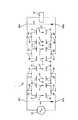
図1から図3は、全体を参照記号1で示す本発明によるトランスの一実施形態を概略的に示す図である。
トランス1は、圧電材料で作成した単一部品で形成された本体2を含む。この圧電材料は当業者に周知の種々の圧電材料のどれでもよいので、その性質についてここでは述べない。
トランス1が動作していないとき、本体2は、互いに平行な、それぞれ図1と図3に示す2つの平行な面3、4を有する円形リングの形状を有する。
【0018】
本体2の外側横表面と内側横表面とは各々、参照記号Aで示される円対称軸を有する直円形シリンダの形状を有する。これらの外側横表面と内側横表面、およびこれらを形成するシリンダを、それぞれ参照記号EおよびIで示す。さらに、これらの表面E、Iと、面3、4の内側輪郭および外側輪郭を形成し、明らかに対称軸である軸Aに中心を置く円である面3、4の平面との交差部をそれぞれ参照記号E1、E2、I1、I2で示す。
【0019】
後で明らかになる理由によって、軸Aと同じ軸、および横表面E、Iを形成するシリンダの直径の算術平均に等しい直径を有する円形シリンダを図2に参照記号Cにより鎖線で示す。さらに、面3、4におけるこのシリンダCの軌跡を図1と図3にそれぞれ参照記号C1およびC2により鎖線で示す。
【0020】
本体2の圧電材料は、軸Aに平行な方向で面3から面4に向かう方向に均一に分極されている。この分極を図2に矢印Pで示す。
トランス2はまた、本体2の面上に配置され、参照記号5〜12で示された8個の電極を含む。
これらの電極のうち、電極5〜8は面3の周辺すなわち円のC1の外側に配置されている。すなわち、これらの電極5〜8は面3の幅の半分より少し小さい幅を占め、各電極は90°よりわずかに小さな中心角内に配置されている。さらに、これらの電極5〜8は互いに電気的に絶縁されている。
【0021】
後で明らかになる理由によって、図1と図3には参照記号N1とN2で2つの平面が示されている。これら2つの平面は、軸Aで交差して4つの90°の角を形成し、一方の面は電極5、6と電極7、8の間を通過し、他方の面は電極5、8と電極6、7の間を通過する。これらの平面N1、N2の軌跡は図1と図3に同じ参照記号により鎖線で示されている。さらに、これらの平面N1、N2によって決められ、それぞれ電極5〜8のうちの1つを含む、4つの空間ゾーンがそれぞれ参照記号Z1〜Z4で示されている。
【0022】
本体2の面3の内側部分の円C1内に電極9〜12が配置され、これらの電極はまた前記面3の幅の半分より少し小さい幅を占め、それらと電極5〜8の間に絶縁スペースを残している。これらの電極9〜12は、また90°よりわずかに小さな中心角内に配置され、それぞれ先に定めたゾーンZ1〜Z4に位置する。
また電極9〜12は互いに電気絶縁されているが、各電極は、参照記号13〜16で示される導電経路によって電極5〜8のうちの1つに接続されている。
さらに正確には、経路13〜16はそれぞれ、電極5と10、電極6と11、電極7と12、および電極8と9を接続する。さらに経路13〜16は、平面N1、N2の軌跡が中間円C1と交差する点の1つをそれぞれが含むように配置されている。
【0023】
トランス1はさらに、本体2の面4上に配置され、参照記号17〜24で示される別の8個の電極を含む。これらの電極17〜24はそれぞれ電極5〜12に面して配置され、したがってこれらの電極に類似のものである。したがって、電極17〜24についてはこれ以上詳しくは説明しない。導電経路25〜28はそれぞれ電極17と22、電極18と23、電極19と24、および電極20と21を接続していることだけを述べておく。さらに、これらの経路25〜28は、平面N1、N2の軌跡が円C2と交差する点の1つをそれぞれが含むように配置されている。
【0024】
図2の断面図に見られる電極6、8、10、12、18、20、22、24の厚さは、図2を見やすくするために、著しく誇張してあることに留意されたい。これらの電極ならびに見えない電極および導電経路13〜16と25〜28は、本体2の面3、4上に非常に薄い金属層を単に付着させることによって従来の方法で行われることが、当業者には理解されよう。
【0025】
トランス1はまた、トランス本体2の振動を励起する電圧をトランスに供給し、この振動によって生ずる電圧を使用する回路に電極5〜12および17〜24を接続する手段も含む。振動およびこの振動がこの電圧を発生させる方法については後で述べる。
この例では、これらの接続手段は、導電性材料で作成されて、それぞれ例えばボンディングによって導電経路13〜16および25〜28の1つに1端部が固定されたロッド29〜36によって形成される。
さらにまた、後で明らかになる理由によって、これらのロッド29〜36は、図1および図3に示すように、平面N1、N2が円C1、C2と交差する点において経路13〜16、25〜28に固定することが好ましい。
【0026】
以下のトランス1の動作に関する記載を読めば、これらのロッド29〜36または少なくともそのうちのいくつかを使用して、トランス1を適当な支持体上に機械的に固定することもできることが、当業者には容易に理解されよう。
トランス1の動作の説明を始める前に、トランス1が互いに垂直をなす2つの対称面S1、S2を含み、これらの平面S1、S2は同時に平面N1、N2によって形成される角を二分する平面であることを強調する。これらの平面S1、S2の軌跡を、図1と図3に同じ参照番号により鎖線で示す。
【0027】
電極5、7、9、11、17、19、21、23の各々は平面S1に対して対称であること、および電極6、8、10、12、18、20、22、24の各々は平面S2に対して対称であることがわかる。さらに、電極5、9、17、21は平面S2に対して電極7、11、19、23に対称であり、かつ電極6、10、18、22は平面S1に関して電極8、12、20、24に対称である。
【0028】
次に上述のトランス1の動作を図4に示した特定の例を用いて記載する。この例に限定することを意味しないのはいうまでもない。
この例では、接続ロッド29、31が互いに電気的に接続され、かつ端子BP1に接続されている。同様に、接続ロッド33、35が互いに電気的に接続され、かつ端子BP2に接続されている。さらにまた、接続ロッド30、32が互いに電気的に接続され、かつ端子BS1に接続され、接続ロッド34、36が互いに電気的に接続され、かつ端子BS2に接続されている。
この接続ロッド29〜36と端子BP1、BP2、BS1、BS2との間の接続は、当業者にはその製造は問題とならないので、さらに詳しくは記載しない。
【0029】
後で明らかになるように、端子BP1、BP2はトランス1に加えられる交流電圧すなわち一次電圧を受け取ることを目的とする。同様に端子BS1、BS2は、トランス1によって発生した電圧すなわち二次電圧をそれらの間に受け取る端子である。これらの一次電圧および二次電圧を、以後それぞれ電圧Up、電圧Usと呼ぶことにする。
【0030】
端子BP1、BP2が実際には存在せず、電圧Upは例えば接続ロッド29、33の両端間に直接加えられることは、当業者には容易に理解されよう。同様に、端子BS1、BS2は存在せず、したがって電圧Usは例えば接続ロッド30、34の両端間に直接受け取られる。
トランス1の電極5〜12、17〜24も、導電経路13〜16、25〜28と同様に極めて概略的に図4に示されている。
【0031】
この場合、電極5、7、10、12は互いに接続され、そして端子BP1に接続され、同様に電極17、19、22、24は端子BP2に接続されている。さらにまた、電極6、8、9、11は互いに接続され、そして端子BS1に接続され、同様に電極18、20、21、23は端子BS2に接続されている。
【0032】
換言すれば、本体2の各々の面3、4の上で、直径方向に向かい合っている2つのゾーンに位置する外側電極が互いに接続され、またそれらは2つの別のゾーンに位置する内側電極に接続されている。こうして、例えば面3の上のゾーンZ1とゾーンZ3とにそれぞれ位置する外側電極5、7は、同じ面3の上に位置するがゾーンZ2とゾーンZ4とにそれぞれ位置する内側電極10、12に接続されている。
【0033】
トランス1に一次交流電圧Upを供給する電源と、トランス1によって供給される二次交流電圧Usが供給される装置を図4においてそれぞれ参照記号41と42で示す。
電源41はどのような様式にすることもできるので、これについては記載しない。さらに、一次電圧Upはどのような波形にすることもできることは、当業者には容易に理解されよう。特に、この電圧Upは正弦波にすることができ、または一般に方形波として分類される波形とすることができる。いずれも、第1定常値と、この第1定常値の絶対値に等しいがこれとは反対の符号を付けた第2定常値とを交互に有する。
【0034】
装置42は、電圧Usなどの交流電圧が供給されるべきさまざまな装置のどの1つであってもよいので、その精密な性質は記載しない。
交流電圧Upによって、電極対5と17、7と19、10と22、12と24のそれぞれの間に位置する本体2の4つの部分に対して電界Fが加えられる。その電界は交流である。以下の説明では、これらの電極5、7、10、12、17、19、22、24を一次電極と呼び、本体2のこれらの電極の部分を本体2の一次部分と呼ぶことにする。
【0035】
電界Fは、軸Aの方向に平行な、したがって本体2の材料の分極方向Pに平行な方向を有し、また交互に分極方向Pと同じ方向および逆方向である方向を有する。
周知の方法で、一般に電気機械結合と呼ばれる電界Fと本体2の材料との横方向電気機械結合によって、先に定義した本体2の4つの一次部分に対して機械的応力が加えられることになる。電界Fは交互に2つの方向を有するので、これらの機械的応力は、やはり周知の方法で、軸Aに垂直なあらゆる方向でのこれら4つの一次部分の収縮と膨張とを起こさせる。
【0036】
先に定義した4つの一次部分の第1および第2部分、すなわち電極5、17および電極7、19のそれぞれの間に位置する部分は、やはり先に定義した4つの一次部分の第1および第2部分にそれぞれ位置する本体2の外側部分、すなわちゾーンZ1、Z3であることがわかる。これらの第1および第2一次部分は平面S2に対して互いに対称であり、またこれらの各々は平面S1に対して対称である。
【0037】
第3および第4一次部分すなわち電極10、22および電極12、24のそれぞれの間に位置する部分は、本体2の第2および第4ゾーンすなわちゾーンZ2およびゾーンZ4にそれぞれ位置する本体2の内側部分であることもわかる。これらの第3および第4一次部分は平面S1に対して互いに対称であり、これらの各々は平面S2に対して対称である。
これら4つの一次部分は同じ応力を受け、それは電界Fに応じて膨張か収縮のいずれかであることは明らかである。
【0038】
これらの一次部分の2つが、平面S2に対して互いに対称であって各々が平面S1に対して対称である本体2の外側部分であること、および他の2つの一次部分が、平面S1に対して互いに対称であって各々が平面S2に対して対称である本体2の内側部分であることのために、一次電圧Upの周波数が後で指定する所定の周波数frに少なくとも実質上等しいときには、上記の交替応力は、後で明らかになる理由によって、双だ円モードと言われる特定のモードの本体2の振動を引き起こす。あとでわかるように、基本共振周波数である周波数frを有するこの双だ円モードは、本体の全体形状が変化しないままである前述の周知のトランス本体の振動モードとは完全に異なる。
【0039】
双だ円振動モードについては、後で図5を参照して詳細に説明する。
図5では本体2の面3だけが見えることに留意すべきである。さらにまた、この面3の上に配置された電極5〜12、導電経路13〜16、および接続ロッド29〜32は、図面を不必要に複雑化しないように図5には示さなかった。
図5には、面3の内側輪郭E1と外側輪郭I1が実線で示されている。これらの輪郭は、本体2が振動していないときには円形である。同様に、中間円C1を鎖線で示す。
【0040】
下記の説明を単純化するために、だ円形シリンダが軸Aに垂直の平面のいずれかと交差することによって形成されるだ円の長径であるもの、または短径であるものをそれぞれ、これから述べるさまざまなだ円形シリンダの長径または短径と呼ぶことに留意されたい。
【0041】
先に述べた本体2の特定の振動モードは、この本体2がそのモードで振動するときには、第1だ円リングと第2だ円リングの形状を交互にとるので、双だ円モードと呼ばれる。これらのだ円リングは後で示すように可変でもある。
換言すれば、本体2がこの双だ円モードで振動すると、その外壁Eは、以後外側だ円形シリンダと呼ぶことにする第1だ円形シリンダと第2だ円形シリンダの形状を交互にとり、この本体2の内壁Iは、以後内側だ円形シリンダと呼ぶことにする別の第1だ円形シリンダと別の第2だ円形シリンダの形状を交互にとる。
【0042】
さらに正確には、第1外側だ円形シリンダと第2外側だ円形シリンダの長径はそれぞれ平面S1、S2に位置し、第1内側だ円形シリンダと第2内側だ円形シリンダの長径も同様である。さらに、第1外側だ円形シリンダと第2外側だ円形シリンダの短径はそれぞれ平面S2、S1に位置し、第1内側だ円形シリンダと第2内側だ円形シリンダの短径も同様である。これらすべての長径と短径は明らかに軸Aに垂直である。
【0043】
さらに、本体2の外壁Eと内壁Iが前記外側だ円形シリンダと内側だ円形シリンダとをそれぞれ交互にとると、これらのだ円形シリンダの各々の長径の長さは規則的に変化し、最小値から最大値に増加し、それからその最小値に減少する。それから外壁Eと内壁Iは、本体2の振動がないときに有する円形シリンダをとった後に、他の外側だ円形シリンダと内側だ円形シリンダの形状になる。
同時に、これらのだ円形シリンダの各々の短径の長さも、規則的であるが逆方向に変化し、この長さは最大値から最小値に減少し、それからその最大値に増加するので、本体2の容積は常に一定に保たれる。
【0044】
本体2が上記の様式で振動すると、中間シリンダCも、以後中間だ円形シリンダと呼ぶことにする第1だ円形シリンダと第2だ円形シリンダとを交互にとり、その長径もまた平面S1、S2にそれぞれ位置し、その短径もまた平面S2、S1にそれぞれ位置することは明らかである。さらにまた、これらの中間だ円形シリンダの長径と短径の長さは、先に述べたものと同様な様式で変化する。
【0045】
前記の外側、内側、および中間だ円形シリンダの各々の長径の最小長さと、これらの短径の最大長さは明らかに、それぞれ振動がない場合の外壁E、内壁I、および中間シリンダCの直径に等しいことにも留意すべきである。これらの長径の最大長さと、これらの短径の最小長さとは、例えば本体2の材料の機械的および電気機械的特徴、一次電圧Upの周波数と振幅などの、さまざまなファクタによって左右される。他のすべてが同じ場合には、これらの長径の最大長さと、これらの短径の最小長さは、電圧Upの周波数が本体2の双だ円共振モードの基本共振周波数frに等しいときに、それぞれそれらの最高値と最低値とを有することは、当業者には容易に理解されよう。
【0046】
図5は、前述のだ円形シリンダと本体2の面3の平面との交差によって形成されるさまざまなだ円の2つの例を示す。これらのだ円は、これらを形成するだ円形シリンダと同じ方法で呼ぶことにする。
したがって図5では、第1外側だ円の一例と第2外側だ円の一例とを点線で示し、それぞれ参照符号E11、E12で示す。
同様に、対応する第1内側だ円と第2内側だ円の例をやはり点線で示し、参照符号I11、I12で示す。
最後に、対応する第1中間だ円と第2中間だ円の例を鎖線で示し、それぞれ参照符号C11、C12で示す。
図5に示すさまざまなだ円は非常に誇張されており、実際には、これらの長径と短径の最大長さと最小長さとの差は、これらの長さの1000分の1以下であることに留意されたい。
【0047】
先に述べた双だ円モードでの本体2の振動は明らかに、電極対6と18、8と20、9と21、11と23との間にそれぞれ位置する本体2の4つの部分への、軸Aに垂直の方向の、交番する機械的な収縮応力と膨張応力の付加を引き起こす。これらの4つの部分を、以下の記載では二次部分と呼ぶことにする。
【0048】
周知の方法で、交番応力と本体2の材料の分極Pとの間の電気機械結合は、これらの二次部分において電界F’を発生させる。この電界F’もまた交番し、これは分極Pの方向と平行な方向を有し、また分極Pの方向と同じ方向とその反対方向とが交番する方向を有する。さらに周知の方法で、この電界F’は、先に列挙した本体2の二次部分となる電極対の両端に、したがってトランス1の端子BS1とBS2との両端に二次交流電圧Usを発生させる。
【0049】
上記の例では、4つの二次部分の第1と第2、すなわち電極9、21の間と電極11と23の間にそれぞれ位置する二次部分は、本体2の内側部分であり、先に定義したゾーンの第1と第2、すなわちゾーンZ1とZ3にそれぞれ位置し、そこには、やはり先に定義した第1および第2一次部分がそれぞれ位置する。これらの第1および第2二次部分も平面S2に関して互いに対称であり、これらの各々は平面S1に対して対称である。
【0050】
同様に、第3と第4二次部分、すなわち電極6、18の間と電極8と20の間にそれぞれ位置する二次部分は、本体2の外側部分であり、先に定義したゾーンの第3と第4、すなわちゾーンZ2とZ4にそれぞれ位置し、そこには、やはり先に定義した第3および第4の一次部分がそれぞれ位置する。これらの第3および第4の二次部分も平面S1に関して互いに対称であり、これらの各々は平面S2に対して対称である。
【0051】
ところで、本体2の材料は軸Aに垂直のすべての方向に等方性である。この結果、この例で一次部分として選ばれた本体2の部分は、同様に二次部分としても選択されることができ、この逆も可能である。
同様に、一次電極として選ばれた電極は、同様に二次電極として選ぶことができ、この逆も可能である。
【0052】
こうして一般に、トランス1の本体2の面3、4の各々は第1および第2一次電極を含み、これらの電極は、平面S1、S2の第1面に対して互いに対称であり、各々が平面S1、S2の第2面に対して対称である外側電極であると言える。
面3、4の各々は第3および第4一次電極も含み、これらの電極は、先に定義した平面の第2面に対して互いに対称であり、各々が前記の平面の第1面に対して対称である内側電極である。
さらに、面3、4の各々は第1および第2二次電極を含み、これらの電極は、先に定義した平面の第1面に対して互いに対称であり、各々が前記の平面の第2面に対して対称である内側電極である。
最後に、面3、4の各々は第3および第4二次電極を含み、これらの電極は、先に定義した平面の第2面に対して互いに対称であり、各々が前記の平面の第1面に対して対称である外側電極である。
【0053】
本体2が前述の双だ円モードで振動すると、やはり先に定義した第1中間双だ円形シリンダは、軸Aに平行な4本の直線に沿って平面N1、N2と交差するということ、その4本の直線は中間円形シリンダが平面N1、N2と交差する直線でもあり、その位置は本体2の振動の振幅がどうであっても固定されることに留意すべきである。さらに、第2中間だ円形シリンダが同じ4本の直線に沿って平面N1、N2と交差する。
【0054】
こうして、これらの4本の直線は本体2の双だ円振動節直線であり、4本の直線が本体2の面3、4の平面と交差する点は前記振動の節点である。これは、接続ロッド29〜32が前述のようにこれらの点で固定されることが好ましいことの理由である。
【0055】
理論的考察をここでは繰り返さないが、この考察は、本体2などのリングの双だ円振動モードの基本共振周波数frは下記の式によって得られることを示す。
【数1】
ただし、Reは、本体2の振動がない場合の本体2の外側半径であり、
αは、やはり本体2の振動がない場合の、本体2の内側半径Riと外側半径Reとの比Ri/Reに依存する解析的に決定される係数であり、
Eは、本体2の材料のヤング率であり、
ρは、本体2の材料の比重であり、
υは、本体2の材料のポアソン比である。
【0057】
図6は、本体2の内側半径Riと外側半径Reとの比Ri/Reの関数として、前記の係数αの変化を示す。この場合には、この係数αは、固形円盤について比Ri/Reがゼロにおける約1.37から比Ri/Reが0.9における約0.17にまで変化していることがわかる。
【0058】
周知であり頻繁に使用される通常PZT(ジルコン酸チタン酸鉛)と呼ばれるセラミック材料が、本体2のための材料として使用される場合には、
E=67・109パスカル
ρ=7.5・103kgm-3
υ=0.3
である。
さらに、例えばそれぞれ8mmと5mmである値が本体2の外側半径Reと内側半径Riのために任意に選択され、したがって比Ri/Reが0.625である場合には、図6は係数αが約0.38の値を有することを示す。
この状況で、上記の式(1)によれば、
fr=23.68kHz
となる。
【0059】
共振周波数が所定の値、例えば25kHzを有し、また半径Reが例えば6mmであることを望む場合には、上の式(1)は、先の例と同じ材料では、係数αは、0.30になるはずである。比Ri/Reは図6にしたがって0.7になるはずである。これは本体2の内側半径Riとして4.2mmの値を与える。
【0060】
上述の理論的考察はまた、トランス1の二次部分が負荷に全く接続されておらず、電圧Upの周波数が上式(1)によって与えられる基本共振周波数に等しいときには、二次電圧Usと一次電圧Upとの間の比、すなわちトランス1のオフロード変圧比Tは下記の式で得られる。
【数2】
kは、この例で使用されすでに述べた結合モードにおける、本体2の材料の有効電気機械結合係数である。
この変圧比Tは本体2の材料の特徴のみに依存し、本体2の寸法には依存しないことがわかる。
本体2の材料が上記の例で述べた材料であるときには、
Q=800
k=0.2
となる。
この場合には、上式(2)にしたがって
T=33.3
となる。
【0061】
本体2の厚さ、すなわち軸Aに平行な方向における本体2の寸法は上の式(1)、(2)に現れないので、共振周波数frと変圧比Tはこのような厚さとは無関係であることに留意すべきである。しかしながら本体2の厚さに明らかに依存する本体2の機械的耐性は、本体2にとって、全く損傷することなく振動中に受ける機械的応力に耐えるように十分でなければならないことは、当業者には理解されよう。
さらに、本体2の厚さがトランス1の一次および二次インピーダンスに影響することも、当業者には理解されよう。
【0062】
本体2がその振動中に受ける機械的応力の値を計算できるようにする、先に挙げた理論的考察は、本体2は一般に1mm程度、または本体2が製造される材料によっては1mm以下の厚さを有することができ、しかもその機械的耐性が不足しないことを示す。この厚さの正確な値は明らかに、一次および二次インピーダンスが所望の値を有するように決定される。
【0063】
図7は本発明によるトランスの別の実施形態を示すもので、この場合、全体的に参照記号51で示されている。
トランス51は、円形リング53、54の形状をなす2つの同じ部分を含む本体52を含み、円形リング53、54は、やはり参照記号Aで示す円対称軸を有する。
リング53、54は、当業者には周知の圧電材料のいずれであってもよい圧電材料で作られ、互いに対面するリング53、54の表面全体を覆う導電材料の薄い金属層を介して互いに固定される。後でわかるように、この金属層は、参照記号55で示す共通電極を形成する。
【0064】
リング53、54の圧電材料は、軸Aに平行な方向に均一に分極されるが、リング53の材料の分極方向は、リング54の材料の分極方向と逆である。図7に示す例では、それぞれ参照記号P1、P2で示す矢印で表されたこれらの分極は、リング53、54の外面56、57から電極55に向かっている。これらの分極P1、P2を同じように反対方向に向けることができるのは、当業者には容易に理解されよう。
【0065】
トランス51はまた、リング53、54の外面56、57の上に配置された電極、これらの電極を接続して対にする導電経路、およびこれらの電極を一次交流電圧と二次交流電圧の供給が目的となる装置とに接続できるようにする接続ロッドを含む。トランス51のこれらの構成部品は、図1と図3に示したトランス1の対応する構成部品と完全に同じであり、またこれらと同じ参照記号で示されているので、ここでは再び説明しないことにする。
【0066】
図8は、上に説明したトランス51を動作させる方法を示す図である。
この場合には、図4に示したトランス1の場合におけるように、接続ロッド29、31が互いに接続され、かつ第1一次端子BP1に接続されている。さらに、接続ロッド33、35も図4の場合におけるように互いに接続されているが、しかしこれらは第1一次端子BP1に接続されている。
同様に、図4の場合のように、接続ロッド30、32は互いに接続され、かつ第1二次端子BS1に接続されている。さらに、接続ロッド34、36も図4の場合におけるように互いに接続されているが、しかしこれらは第1二次端子BS1に接続されている。
最後に、共通電極55が第2一次端子BP2と第2二次端子BS2とに接続されている。
【0067】
やはりUpで示す一次電圧を供給することを目的とする電源、およびトランス51がやはりUsで示す二次電圧を供給すべき装置も、図8では図4の場合と同様に、それぞれ同じ参照記号41と42で示されている。
【0068】
先に述べたトランス1に類似して、共通電極55と電極5、7、10、12との間に位置するリング53の部分をリング53の一次部分と呼ぶ。同様に、共通電極55と電極17、19、22、24との間に位置するリング54の部分をリング54の一次部分と呼ぶ。さらに、リング53の一次部分の1つとこれに面して位置するリング54の一次部分とによって形成される本体52の部分を本体の一次部分と呼ぶ。したがって本体52の一次部分は、電極対5と17、7と19、10と22、および12と24の間にそれぞれ位置する。これらの電極5、7、10、12、17、19、22、24を一次電極と呼ぶ。
【0069】
また先に述べたトランス1に類似して、共通電極55と電極6、8、9、11との間に位置するリング53の部分をリング53の二次部分と呼ぶ。同様に、共通電極55と電極18、20、21、23との間に位置するリング54の部分をリング54の二次部分と呼ぶ。さらに、リング53の二次部分の1つとこれに面して位置するリング54の二次部分とによって形成される本体52の部分を本体の二次部分と呼ぶ。したがって本体52のこれらの二次部分は、電極対6と18、8と20、9と21、および11と23の間にそれぞれ位置する。これらの電極6、8、9、11、18、20、21、23を二次電極と呼ぶ。
【0070】
本体52の一次部分と二次部分は、正確にトランス1の本体2と同じ相互関係で配置されている。同様に、本体52の面56、57の各々の上には、一次電極と二次電極とが、正確にトランス1の本体2の面3、4の上に位置するものと同じ相互関係で配置されている。
【0071】
一次電圧Upに応じてリング53とリング54の一次部分にそれぞれ発生する電界F1、F2は常に、同時に、それぞれの分極P1、P2と同じ方向またはこの分極の方向と反対の方向のいずれかを有することもわかる。
【0072】
こうして、電界F1とリング53の材料との、および電界F2とリング54の材料との横方向電気機械結合は、前記リング53、54の一次部分すべての上に同じ機械的応力を付加させ、そしてこれらの応力は、軸Aに垂直なあらゆる方向への前記一次部分の収縮と膨張とを交互に引き起こす。
【0073】
リング53とリング54の一次部分は、先に定義したように対として本体52の一次部分を形成し、この結果、一次電圧Upの周波数が少なくとも実質的に式(1)によって先に決定された周波数frと同じときには、トランス51の本体52も、トランス1の場合でも先に記載した双だ円モードで振動する。したがって、この双だ円モード振動をここで再度説明はしない。
【0074】
同様に、トランス51の本体52がこの双だ円モードで振動すると、リング53、54の二次部分は同様に同じ機械的応力を受けるので、これらの二次部分の中に発生する電界F1’、F2’は常に、それぞれの分極P1、P2と同じ方向またはこの分極P1、P2の方向と反対の方向のいずれかを有する。
したがって、これらの電界F1’、F2’に応じて一方では共通電極55と電極6、8、9、11との間に、また他方では共通電極55と電極18、20、21、23との間に発生する電圧は、常に同じ極性を有し、一緒に二次電圧Usを形成する。
電圧UsとUpとの比すなわちトランス51の変圧比Tは、前述の式(2)によっても得られ、したがってこれは前述のトランス1の変圧比と同じである。
【0075】
図9は、図7を参照して説明したトランス51の別の動作方法を示す。
この場合には、接続ロッド29、31が互いに接続され、第1一次端子BP1aに接続され、接続ロッド30、32が互いに接続され、第2一次端子BP1bに接続されている。
共通電極55は第3一次端子BP2に接続されている。
【0076】
やはりこの場合でも、接続ロッド33、35が互いに接続され、第1二次端子BS1に接続され、接続ロッド34、36が互いに接続され、第2二次端子BS2に接続されている。
【0077】
この場合には、トランス51は61で示す電源によって電力が供給される。この電源61は一次電圧Upを形成する2つの交流電圧Up1、Up2と一緒に供給し、これらの電圧は同じ周波数と同じ振幅とを有するが、互いに180°の位相差がある。言い換えれば、これらの電圧Up1、Up2は常に互いに相反する極性を有する。この電源61は、この実現を当業者が理解できるので詳しくは記載しない。
【0078】
電源61は端子BP1a、BP1b、およびBP2に、電圧Up1が端子BP1aと端子BP2の間に印加され、電圧Up2が端子BP1bと端子BP2の間に印加されるように接続されている。
【0079】
この場合、本体52の一次部分は2つの群を形成し、このうちの第1群は、共通電極55と電極5、7、10、12との間に位置する一次部分によって形成され、第2群は、共通電極55と電極6、8、9、11との間に位置する一次部分によって形成される。
【0080】
同様に、本体52の二次部分も2つの群を形成し、このうちの第1群は、共通電極55と電極17、19、22、24との間に位置する二次部分によって形成され、第2群は、共通電極55と電極18、20、21、23との間に位置する二次部分によって形成される。
【0081】
この実施形態の場合にはこうして、一次部分のすべてと二次部分のすべては、それぞれリング53とリング54とに属する。
第1群の一次部分と第2群の一次部分においては、電圧Up1、Up2に応じて発生したそれぞれの電界F1、F2が常に互いに相反する方向を有し、これらの電界F1、F2の各々もまた、リング53の材料の分極P1と同じ方向または前記分極P1の方向と反対の方向のいずれかを有する。
【0082】
この結果、第1群の一次部分が例えば機械的膨張応力を受けると、第2群の一次部分が機械的収縮応力を受け、またその逆となる。
ゾーンZ1、Z3の各々において、外側部分すなわち電極5、7に対面してそれぞれ位置する部分が、これらの一次部分の第1群に属し、内側部分すなわち電極9、11に対面してそれぞれ位置する部分が、一次部分の第2群に属することもわかる。
同様に、別のゾーンZ2、Z4の各々において、外側部分すなわち電極6、8に対面してそれぞれ位置する部分は、これらの一次部分の第2群に属し、内側部分すなわち電極10、12に対面してそれぞれ位置する部分が、一次部分の第1群に属する。
【0083】
この結果、一般に、2つの直径方向に対向するゾーンZ1〜Z4に位置する外側部分が、例えば収縮応力を受けると、同じゾーンに位置する内側部分は膨張応力を受ける。さらに、2つの別のゾーンに位置する外側部分は膨張応力を同時に受け、これらのゾーンに位置する内側部分は圧縮応力を受ける。
【0084】
本体52のさまざまな一次部分におけるこの応力分布の効果は、電圧Up1、Up2の周波数が先に式(1)によって決定された周波数frに少なくとも実質的に等しいときに、本体52が前述の双だ円モードで振動することである。
同様に、トランス51の本体52がこの双だ円モードで振動して、第1群の二次部分がこの振動に応じて例えば機械的膨張応力を受けると、第2群の二次部分は機械的収縮応力を受け、またこの逆もある。
【0085】
この結果、第1群のこれらの二次部分と第2群のこれらの二次部分にそれぞれ発生した電界F1’、F2’は、常に互いに相反する方向を有する。さらに、これらの電界F1’、F2’に応じて一方では共通電極55と電極17、19、22、24との間に、他方では共通電極55と電極18、20、21、23との間に発生した電圧は、明らかに同じ周波数と同じ振幅とを有し、常に互いに相反する方向を有する。
【0086】
接続ロッド33〜36が、先に説明し図9に示す様式で接続されると、これら2つの電圧は一緒になって、トランス51によって発生される二次電圧Usを形成する。
この場合、トランスの変圧比Tも前述の式(2)によって得られる。
同等の空間要件では、本実施形態によるトランス本体の双だ円モードの基本共振周波数は、先に述べた周知のトランスの本体の振動モードの基本共振周波数よりも著しく低いことがわかる。
【0087】
こうして、本発明によるトランスは、周知のトランスが供給する周波数よりも著しく低い周波数を有する二次電圧を供給することができる。
しかも、本発明によるトランスの変圧比は周知のトランスのそれと同じ程度か、またはそれよりも高い。
【0088】
本発明によるトランスは、使用可能空間が限られた腕時計などの装置や、比較的低い周波数を有する比較的高い交流電圧を得ることが必要なすべての場合などにおける使用に特によく適合する。
【0089】
さらに、本発明によるトランス本体またはこの本体を形成する各部品を作るための圧電材料が、その面に垂直な方向に均一に分極されるという事実は、前記本体の製造を簡単にし、トランスのコスト価格を節減する。
【0090】
本発明によるトランスの実施形態を記載したが、本発明の範囲を逸脱することなく、本発明によるトランスの多くの変更が可能であることは明らかである。
【0091】
こうして、例えば、本発明によるトランスの本体に中央開口を設けることなく固形ディスクの形状を与えることは可能であり、このディスクを図1〜図3のトランス1の本体2のような単一部分として作ることができ、または図7のトランス1の本体52のような2つの同じ部分として形成することができる。
【0092】
同様に、本発明によるトランスの本体の上に配置されたさまざまな電極は、記載した例のものとは異なる形状を有することもでき、これらの接続部も異なった様式で達成することができる。
【0093】
先に記載した例におけるように多くの二次電極を設けることは、強制的でないことも当業者には理解されよう。実際に、単に一対の二次電極、例えば図4と図8の電極6と18、または11と23、または図9の電極17と18、または21と22を準備しても十分である。
【図面の簡単な説明】
【図1】 本発明実施形態による圧電トランスの第1面の概略図である。
【図2】 図1のトランスの図1の軸のII−IIに沿った概略断面図である。
【図3】 図1のトランスの第2面の概略図である。
【図4】 図1〜図3のトランスの動作方法を示す概略図である。
【図5】 図1〜図3のトランス本体の変形を示す概略図である。
【図6】 図1〜図3のトランス本体の特性を示す概略図である。
【図7】 本発明によるトランスの別の実施形態を示す概略図である。
【図8】 図7のトランスの動作方法を示す概略図である。
【図9】 図7のトランスの別の動作方法を示す概略図である。
【符号の説明】
1 トランス
2 本体
3 本体の第1面
4 本体の第2面
5〜12 電極
13〜16 電極
17〜24 電極
25〜28 導電経路
29〜36 接続ロッド
41 電源
42 装置
53 円形リング
54 円形リング
55 共通電極
56 円形リングの外面
57 円形リングの外面
61 電源[0001]
BACKGROUND OF THE INVENTION
The present invention
A body made of a piezoelectric material having a first surface, a second surface, and an outer lateral surface;
A plurality of primary electrodes disposed on the body and vibrating the body in response to a primary alternating voltage;
A plurality of secondary electrodes disposed on the body and generating a secondary voltage in response to vibration;
The outer lateral surface is in the form of a first circular cylinder with an axis of symmetry when there is no vibration, and the first and second surfaces are an outer portion located on the outer lateral surface side and an outer portion. Having an enclosed inner portion,
The present invention relates to a piezoelectric transformer.
[0002]
[Prior art]
A piezoelectric transformer having these features is disclosed in U.S. Pat. No. 2,974,296 and shown in FIG. The body of this transformer has the shape of an elongated hollow circular cylinder polarized in the axial direction. A primary voltage is applied longitudinally between the two electrodes surrounding the body, on both sides of its center, thereby causing the body to vibrate in the longitudinal mode. The secondary voltage is at one of the ends of the body and is received between two electrodes surrounding the body.
In addition to the following deficiencies common to all known transformers, this transformer has the disadvantage that it is relatively difficult to manufacture in large quantities due to the shape of an elongated hollow cylinder. The cost is therefore relatively high.
[0003]
Another transformer having the above characteristics is disclosed in the same U.S. Pat. No. 2,974,296 and shown in FIG. The body of this transformer has the shape of a circular disc, the central part of which is axially polarized and the outer annular part is radially polarized. A primary voltage is applied between two electrodes located on either side of the central portion of the body, thereby causing the body to vibrate in a radial mode. A secondary voltage is received between one of these electrodes and a third electrode disposed on the lateral surface of the body.
[0004]
Yet another transformer having the above features is disclosed in the same US Pat. No. 2,974,296 and shown in FIG. The body of this transformer has the shape of a circular ring, the first half of which is axially polarized in plan view. The second half of the ring is formed of two tangentially polarized portions, the polarization directions of the two portions being opposite to each other. The primary voltage is applied between two electrodes arranged on either side of the first half of the ring, whereby the body vibrates in a so-called tangential mode. A secondary voltage is received between one of these two electrodes and the third electrode, which surrounds the second half of the ring where the two parts polarized in opposite directions join. It is out.
[0005]
The above two transformers have the disadvantage that they are relatively difficult to manufacture because their bodies have multiple parts that must be polarized differently. Therefore, these costs are relatively high.
[0006]
The means for supplying the primary voltage necessary to operate the above-mentioned known transformer is clearly configured so that the body of the transformer vibrates at one of its vibration mode resonance frequencies. The frequency of the secondary voltage generated in response to this vibration is clearly the same as the frequency of this vibration. Therefore, the lowest frequency of the secondary voltage is the same as the fundamental resonance frequency of the mode in which the transformer body vibrates.
[0007]
In general, the fundamental resonant frequency of an object that vibrates in one of the object's vibration modes, and in particular the piezoelectric transformer body, in particular depends on the dimensions of the object, and if all else is the same, the dimensions of that object It is known that the basic resonance frequency increases with decreasing.
[0008]
From the above and the characteristics of the above-mentioned known transformers, as a result, the basics of the transformer body when one of these known transformers is to be used in a device where the available space is very limited. The resonant frequency must be high, and of course the secondary voltage supplied by the transformer must also be high.
[0009]
An example of such a device with very limited usable space is a wristwatch. In this case, many components must be accommodated in a case whose inner diameter is generally 3 to 4 cm or less.
[0010]
When trying to place a conventional piezoelectric transformer as described above in a wristwatch, the dimensions of the body of the transformer are such that the basic resonance frequency of the body, and therefore the lowest resonance frequency of the secondary voltage generated by the transformer exceeds 100 kilohertz, One skilled in the art will readily appreciate that in some cases it must be small enough to reach several megahertz.
The use of such high frequency AC voltages can cause problems.
That is, for example, losses due to stray capacitances inevitably formed by various conductors receiving this voltage can be excessive, and these stray capacitances can interfere with the normal operation of the device.
Similarly, the power consumption of a circuit that supplies a transformer with a primary voltage that must clearly have the same frequency as the secondary voltage is likely to be excessive because the higher the frequency, the higher the power consumption. .
[0011]
Furthermore, a voltage having such a high frequency cannot be used for any purpose.
That is, for example, it is well known that an illuminating device or electroluminescent display device that is often advantageous for use in a wristwatch must be supplied with an alternating voltage having an amplitude of several tens of volts. A wristwatch is typically powered by a battery or accumulator that supplies a direct current (DC) voltage on the order of 1.5-3 volts. Such a DC voltage can be easily converted to an AC voltage using a simple electronic circuit, and the amplitude of this AC voltage is clearly about 1.5 to 3 volts.
[0012]
There is a need to prepare a transformer to supply energy to the electroluminescent device in the wristwatch, and the piezoelectric transformer at first glance appears to be particularly well suited for such applications.
However, it is also known that the lifetime of an electroluminescent device decreases rapidly when the frequency of the supply voltage exceeds several tens of kilohertz, for example 30-40 kilohertz. Therefore, since the frequency of the voltage supplied from a known piezoelectric transformer is too high for such a device, the voltage cannot be supplied by such a piezoelectric transformer.
[0013]
It should be noted that other piezoelectric transformers are also disclosed in the aforementioned U.S. Pat. Nos. 2,974,296, 5,241,236, 5,365,141, 5,371,430 and 5,440,195. However, in these transformers, when the required space is small, the fundamental resonance frequency of the vibration mode of the main body becomes very high, so these transformers cannot be used to solve the above-mentioned problems. Furthermore, it should be noted that the body of all these transformers has a parallelepiped shape and therefore does not meet the general definition described above.
[0014]
[Problems to be solved by the invention]
The object of the present invention is therefore to have sufficiently small dimensions that can easily be used in devices that meet this general definition and have limited space available, and the secondary voltage generated is the same. To provide a piezoelectric transformer configured so that its body vibrates in a mode with a sufficiently low fundamental frequency that can be used even if the frequency of the secondary voltage generated by a known transformer with spatial requirements is too high It is.
[0015]
[Means for Solving the Problems]
The object includes a body made of a piezoelectric material having a first surface, a second surface, and an outer lateral surface, and a plurality of primary electrodes disposed on the body and oscillating the body in response to a primary AC voltage; A plurality of secondary electrodes disposed on the body and generating a secondary voltage in response to vibration, the outer lateral surface having the shape of a first cylinder having an axis of symmetry when there is no vibration; Each of the first surface and the second surface has an outer portion located on the side surface side of the outer lateral surface and an inner portion surrounded by the outer portion, and the primary electrode has a primary voltage at least substantially at a predetermined frequency. When having the same frequency, the outer lateral surface is arranged to alternate between the shape of the first oval cylinder and the shape of the second oval cylinder, the first oval cylinder having a major axis perpendicular to the symmetry axis and A major axis having a minor axis, the major axis including a first axis of symmetry. In the nominal plane, the minor axis is in the second symmetry plane perpendicular to the first symmetry plane and also including the symmetry axis, the second elliptic cylinder has a major axis and a minor axis perpendicular to the symmetry axis; When the major axis is in the second symmetry plane, the minor axis is in the first symmetry plane, and the outer lateral surface has one of the shapes of the first and second oval cylinders, the respective major axis is , Having a length that varies regularly from the minimum to the maximum equal to the diameter of the circular cylinder and then decreases from the maximum to the minimum, after which the outer lateral surface is the first and This is achieved by a piezoelectric transformer characterized by taking a shape different from that of the second oval cylinder.
[0016]
Other objects and advantages of the present invention will become apparent from the following description of selected embodiments of the present invention, given below by way of non-limiting example and with reference to the accompanying drawings.
[0017]
DETAILED DESCRIPTION OF THE INVENTION
1 to 3 schematically show an embodiment of a transformer according to the invention, indicated generally by the
The
When the
[0018]
The outer lateral surface and the inner lateral surface of the
[0019]
For reasons that will become apparent later, a circular cylinder having the same axis as axis A and a diameter equal to the arithmetic mean of the diameters of the cylinders forming the transverse surfaces E, I is shown in FIG. Further, the trajectory of the cylinder C on the
[0020]
The piezoelectric material of the
The
Of these electrodes, the
[0021]
For reasons that will become apparent later, FIGS. 1 and 3 show two planes with reference symbols N1 and N2. These two planes intersect at axis A to form four 90 ° corners, one face passing between
[0022]
Electrodes 9-12 are arranged in a circle C1 in the inner part of the
The electrodes 9-12 are electrically insulated from each other, but each electrode is connected to one of the electrodes 5-8 by a conductive path indicated by reference symbols 13-16.
More precisely, the
[0023]
The
[0024]
Note that the thickness of the
[0025]
The
In this example, these connecting means are formed by rods 29-36 made of a conductive material and fixed at one end to one of the conductive paths 13-16 and 25-28, respectively, for example by bonding. .
Furthermore, for reasons that will become apparent later, these rods 29-36 are connected to paths 13-16, 25- 25 at the points where planes N1, N2 intersect circles C1, C2, as shown in FIGS. It is preferable to fix to 28.
[0026]
Those skilled in the art will be able to mechanically fix the
Before starting the description of the operation of the
[0027]
Each of the
[0028]
Next, the operation of the above-described
In this example, the connecting
The connection between the connecting
[0029]
As will become apparent later, the terminals BP1 and BP2 are intended to receive an alternating voltage or primary voltage applied to the
[0030]
One skilled in the art will readily appreciate that the terminals BP1, BP2 do not actually exist and the voltage Up is applied directly across the connecting
The electrodes 5-12, 17-24 of the
[0031]
In this case, the
[0032]
In other words, on each
[0033]
A power source for supplying the primary AC voltage Up to the
The
[0034]
Since the
The AC voltage Up applies an electric field F to the four portions of the
[0035]
The electric field F has a direction parallel to the direction of the axis A, and thus parallel to the polarization direction P of the material of the
In a known manner, a mechanical stress is applied to the four primary parts of the
[0036]
The first and second parts of the four primary parts defined above, ie the part located between each of the
[0037]
The third and fourth primary parts, i.e. the parts located between the
It is clear that these four primary parts are subjected to the same stress, which is either expansion or contraction depending on the electric field F.
[0038]
Two of these primary parts are the outer parts of the
[0039]
The double elliptical vibration mode will be described later in detail with reference to FIG.
It should be noted that only the
In FIG. 5, the inner contour E1 and the outer contour I1 of the
[0040]
In order to simplify the following description, the various ellipse cylinders that are the major axis or minor axis of the ellipse formed by intersecting any of the planes perpendicular to the axis A will be described below. Note that it is referred to as the major or minor diameter of a round cylinder.
[0041]
The specific vibration mode of the
In other words, when the
[0042]
More precisely, the major axis of the first outer ellipse cylinder and the second outer ellipse cylinder are located on the planes S1 and S2, respectively, and the major axis of the first inner ellipse cylinder and the second inner ellipse cylinder are the same. Further, the short diameters of the first outer oval cylinder and the second outer oval cylinder are respectively located on the planes S2 and S1, and the short diameters of the first inner oval cylinder and the second inner oval cylinder are the same. All these major and minor axes are clearly perpendicular to axis A.
[0043]
Furthermore, when the outer wall E and the inner wall I of the
At the same time, the length of the minor axis of each of these oval cylinders also changes in a regular but opposite direction, and this length decreases from maximum to minimum and then increases to its maximum The volume of 2 is always kept constant.
[0044]
When the
[0045]
Obviously, the minimum length of each major axis of the outer, inner and middle elliptical cylinders and the maximum length of these minor diameters are the diameters of the outer wall E, inner wall I and intermediate cylinder C, respectively, when there is no vibration. Note also that it is equal to. The maximum length of these major diameters and the minimum length of these minor diameters depend on various factors such as the mechanical and electromechanical characteristics of the material of the
[0046]
FIG. 5 shows two examples of various ellipses formed by the intersection of the aforementioned elliptic cylinder and the plane of the
Accordingly, in FIG. 5, an example of the first outer ellipse and an example of the second outer ellipse are indicated by dotted lines and indicated by reference numerals E11 and E12, respectively.
Similarly, examples of the corresponding first inner ellipse and second inner ellipse are also indicated by dotted lines and indicated by reference numerals I11 and I12.
Finally, examples of the corresponding first intermediate ellipse and second intermediate ellipse are indicated by chain lines, and are indicated by reference numerals C11 and C12, respectively.
The various ellipses shown in FIG. 5 are greatly exaggerated, and in fact, the difference between the maximum and minimum lengths of these major and minor axes is less than one thousandth of these lengths. Please note that.
[0047]
The vibration of the
[0048]
In a known manner, the electromechanical coupling between the alternating stress and the polarization P of the material of the
[0049]
In the above example, the first and second of the four secondary parts, i.e. the secondary parts located between the
[0050]
Similarly, the third and fourth secondary parts, i.e. the secondary parts located between the
[0051]
By the way, the material of the
Similarly, the electrode selected as the primary electrode can be similarly selected as the secondary electrode, and vice versa.
[0052]
Thus, in general, each of the
Each of the
Furthermore, each of the
Finally, each of the
[0053]
When the
[0054]
Thus, these four straight lines are the bi-circular vibration nodal lines of the
[0055]
Although the theoretical consideration is not repeated here, this consideration shows that the fundamental resonant frequency fr of the double elliptical vibration mode of the ring such as the
[Expression 1]
However, Re is an outer radius of the
α is an analytically determined coefficient depending on the ratio Ri / Re between the inner radius Ri and the outer radius Re of the
E is the Young's modulus of the material of the
ρ is the specific gravity of the material of the
υ is the Poisson's ratio of the material of the
[0057]
FIG. 6 shows the change of the coefficient α as a function of the ratio Ri / Re between the inner radius Ri and the outer radius Re of the
[0058]
When a well-known and frequently used ceramic material called PZT (lead zirconate titanate) is used as the material for the
E = 67.109Pascal
ρ = 7.5 · 10Threekgm-3
υ = 0.3
It is.
Further, for example, values of 8 mm and 5 mm, respectively, are arbitrarily selected for the outer radius Re and the inner radius Ri of the
In this situation, according to equation (1) above,
fr = 23.68 kHz
It becomes.
[0059]
If it is desired that the resonant frequency has a predetermined value, for example 25 kHz, and the radius Re is, for example, 6 mm, the above equation (1) is the same material as the previous example, and the coefficient α is 0. Should be 30. The ratio Ri / Re should be 0.7 according to FIG. This gives a value of 4.2 mm as the inner radius Ri of the
[0060]
The above theoretical considerations also show that when the secondary part of the
[Expression 2]
k is the effective electromechanical coupling coefficient of the material of the
It can be seen that the transformation ratio T depends only on the characteristics of the material of the
When the material of the
Q = 800
k = 0.2
It becomes.
In this case, according to the above equation (2)
T = 33.3
It becomes.
[0061]
Since the thickness of the
Furthermore, those skilled in the art will also understand that the thickness of the
[0062]
The theoretical considerations listed above that allow the
[0063]
FIG. 7 shows another embodiment of a transformer according to the invention, which is generally indicated by the
The
[0064]
The piezoelectric material of the
[0065]
The
[0066]
FIG. 8 is a diagram showing a method for operating the
In this case, as in the case of the
Similarly, as in the case of FIG. 4, the connecting
Finally, the
[0067]
A power source intended to supply a primary voltage also indicated by Up and a device to which the
[0068]
Similar to the
[0069]
Similar to the
[0070]
The primary and secondary parts of the
[0071]
The electric fields F1, F2 respectively generated in the primary part of the
[0072]
Thus, the transverse electromechanical coupling between the electric field F1 and the material of the
[0073]
The primary part of the
[0074]
Similarly, when the
Therefore, depending on these electric fields F1 ′, F2 ′, on the one hand, between the
The ratio between the voltage Us and Up, that is, the transformation ratio T of the
[0075]
FIG. 9 shows another method of operating the
In this case, the connecting
The
[0076]
Also in this case, the connecting
[0077]
In this case, the
[0078]
The
[0079]
In this case, the primary part of the
[0080]
Similarly, the secondary part of the
[0081]
In this embodiment, all of the primary parts and all of the secondary parts thus belong to the
In the primary part of the first group and the primary part of the second group, the electric fields F1 and F2 generated according to the voltages Up1 and Up2 always have directions opposite to each other, and each of these electric fields F1 and F2 is also Further, it has either the same direction as the polarization P1 of the material of the
[0082]
As a result, when the primary part of the first group is subjected to, for example, mechanical expansion stress, the primary part of the second group is subjected to mechanical contraction stress and vice versa.
In each of the zones Z1 and Z3, the outer part, that is, the part respectively facing the
Similarly, in each of the other zones Z2, Z4, the part located respectively facing the outer part, i.e. the
[0083]
As a result, generally, when the outer portion located in the two diametrically opposed zones Z1 to Z4 receives, for example, contraction stress, the inner portion located in the same zone receives expansion stress. Furthermore, the outer parts located in two separate zones are simultaneously subjected to expansion stresses and the inner parts located in these zones are subject to compressive stresses.
[0084]
The effect of this stress distribution in the various primary parts of the
Similarly, when the
[0085]
As a result, the electric fields F1 'and F2' generated in these secondary parts of the first group and these secondary parts of the second group always have directions opposite to each other. Furthermore, depending on these electric fields F1 ′, F2 ′, between the
[0086]
When the connecting rods 33-36 are connected in the manner described above and shown in FIG. 9, these two voltages together form a secondary voltage Us generated by the
In this case, the transformation ratio T of the transformer is also obtained by the above equation (2).
Under equivalent space requirements, it can be seen that the fundamental resonance frequency of the double elliptical mode of the transformer body according to the present embodiment is significantly lower than the fundamental resonance frequency of the vibration mode of the known transformer body described above.
[0087]
Thus, the transformer according to the invention can supply a secondary voltage having a frequency significantly lower than that provided by known transformers.
Moreover, the transformer ratio of the transformer according to the invention is as high as or higher than that of known transformers.
[0088]
The transformer according to the invention is particularly well suited for use in devices such as watches with limited available space or in all cases where it is necessary to obtain a relatively high alternating voltage with a relatively low frequency.
[0089]
Furthermore, the fact that the piezoelectric material for making the transformer body according to the invention or the parts forming this body is uniformly polarized in a direction perpendicular to its plane simplifies the production of the body and reduces the cost of the transformer. Save money.
[0090]
While embodiments of a transformer according to the present invention have been described, it will be apparent that many variations of the transformer according to the present invention are possible without departing from the scope of the present invention.
[0091]
Thus, for example, it is possible to give the shape of a solid disk without providing a central opening in the body of the transformer according to the invention, this disk being made as a single part like the
[0092]
Similarly, the various electrodes arranged on the body of the transformer according to the invention can have different shapes than those of the described example, and these connections can also be achieved in different ways.
[0093]
One skilled in the art will also appreciate that providing a number of secondary electrodes as in the example described above is not compulsory. In practice, it is sufficient to simply provide a pair of secondary electrodes, for example,
[Brief description of the drawings]
FIG. 1 is a schematic view of a first surface of a piezoelectric transformer according to an embodiment of the present invention.
2 is a schematic cross-sectional view of the transformer of FIG. 1 taken along the line II-II of FIG.
3 is a schematic view of a second surface of the transformer of FIG. 1. FIG.
FIG. 4 is a schematic diagram illustrating an operation method of the transformer of FIGS.
FIG. 5 is a schematic view showing a modification of the transformer main body of FIGS.
6 is a schematic diagram showing characteristics of the transformer main body of FIGS. 1 to 3. FIG.
FIG. 7 is a schematic diagram showing another embodiment of a transformer according to the present invention.
8 is a schematic diagram illustrating a method of operating the transformer of FIG.
9 is a schematic diagram illustrating another method of operating the transformer of FIG.
[Explanation of symbols]
1 transformer
2 body
3 First side of the body
4 Second side of the body
5-12 electrodes
13-16 electrodes
17-24 electrodes
25-28 conductive path
29-36 Connecting rod
41 Power supply
42 devices
53 Round Ring
54 Circular ring
55 Common electrode
56 External surface of circular ring
57 External surface of circular ring
61 Power supply
Claims (14)
Translated fromJapanese前記本体上に配置され、一次交流電圧に応答して前記本体を振動させる複数の一次電極と、
前記本体上に配置され、前記振動に応答して二次電圧を発生させる複数の二次電極とを含み、
前記外側横表面は、前記振動がないときには、円対称軸を有する円形シリンダの形状を有し、前記第1面及び第2面はそれぞれ、前記外側横表面の側面に位置する外側部分と、この外側部分に囲まれた内側部分とを有し、
前記一次電極は、前記円対称軸を含む第1対称面と前記第1対称面に直交するとともに前記円対称軸を同様に含む第2対称面とを有する対称な外形をなすように配置され、そして前記一次電圧の周波数が少なくとも所定の周波数に等しいときに、前記外側横表面が第1だ円形シリンダの形状と第2だ円形シリンダの形状とを交互にとり、前記第1だ円形シリンダは、前記円対称軸に垂直な長径と短径とを有し、その長径は第1対称面内にあり、また短径は第2対称面内にあり、前記第2だ円形シリンダは、前記円対称軸に垂直な長径と短径とを有し、その長径は前記第2対称面内にあり、またその短径は前記第1対称面内にあり、前記外側横表面が前記第1および第2だ円形シリンダの一方の形状を有するとき、それぞれの長径は、前記円形シリンダの直径に等しい最小値から最大値まで増加し、次いで前記最大値から前記最小値に減少して規則的に変化する長さを有し、その後、前記外側横表面は前記第1および第2だ円形シリンダの他方の形状となる、
圧電トランス。A body made of a piezoelectric material having a first surface, a second surface, and an outer lateral surface;
A plurality of primary electrodes disposed on the body and oscillating the body in response to a primary alternating voltage;
A plurality of secondary electrodes disposed on the body and generating a secondary voltage in response to the vibration;
The outer lateral surface has a shape of a circular cylinder having an axis of circular symmetry when there is no vibration, and the first surface and the second surface are respectively an outer portion located on a side surface of the outer lateral surface, An inner part surrounded by an outer part,
The primary electrode is disposed so as to form a symmetrical outer shape having a first symmetry plane including the circular symmetry axis and a second symmetry plane perpendicular to the first symmetry plane and including the circular symmetry axis in the same manner. When the frequency of the primary voltage is at least equal to a predetermined frequency, the outer lateral surface alternately takes the shape of a first oval cylinder and the shape of a second oval cylinder, and the first oval cylinder The major axis has a major axis and a minor axis perpendicular to the circular symmetry axis, the major axis is in the first symmetry plane, the minor axis is in the second symmetry plane, and the second ellipse cylinder has the circular symmetry axis. The major axis is in the second plane of symmetry, the minor axis is in the first plane of symmetry, and the outer lateral surface is the first and second. When having one shape of a circular cylinder, each major axis is the circular shape It has a length that increases from a minimum value to a maximum value equal to the diameter of Linda and then decreases from the maximum value to the minimum value and then varies regularly, after which the outer lateral surface has the first and second The other shape of the oval cylinder,
Piezoelectric transformer.
それぞれ前記第1対称面に対して対称であり、前記第2対称面に対して互いに対称であり、共に前記本体の前記第1面の前記外側部分に配置されている第1および第2の一次電極と、
それぞれ前記第2対称面に対して対称であり、前記第1対称面に対して互いに対称であり、共に前記本体の前記第1面の前記内側部分に配置されている第3および第4の一次電極と、
すべて前記本体の前記第2面上に配置され、それぞれ前記第1、第2、第3、第4の一次電極に面している、第5、第6、第7、および第8の一次電極と
を含む請求項2または3に記載の圧電トランス。The plurality of primary electrodes,
First and second primary respectively symmetric with respect to the first symmetry plane and symmetrical with each other with respect to the second symmetry plane, both disposed on the outer portion of the first face of the body. Electrodes,
Third and fourth primary respectively symmetrical with respect to the second symmetry plane, symmetrical with respect to the first symmetry plane, and both disposed on the inner portion of the first face of the body. Electrodes,
Fifth, sixth, seventh, and eighth primary electrodes, all disposed on the second surface of the body and facing the first, second, third, and fourth primary electrodes, respectively. The piezoelectric transformer according to claim 2, comprising:
それぞれ前記本体の前記第1面および前記第2面上で互いに対面して配置され、前記第1対称面に対してそれぞれ前記第1の二次電極および前記第2の二次電極に対称である第3および第4の二次電極と、
それぞれ前記本体の前記第1面および前記第2面上で互いに対面して配置され、それぞれ前記第3の一次電極と前記第4の一次電極との間および前記第7の一次電極と前記第8の一次電極との間の位置する、第5および第6の二次電極と、
それぞれ前記本体の前記第1面と前記第2面上で互いに対面して配置され、前記第2対称面に対して第5および第6の二次電極に対称である第7および第8の二次電極と
をさらに含む請求項6に記載の圧電トランス。The plurality of secondary electrodes are
Respectively disposed on the first surface and the second surface of the main body so as to face each other and symmetrical to the first secondary electrode and the second secondary electrode, respectively, with respect to the first symmetry plane Third and fourth secondary electrodes;
The first and second surfaces of the main body are arranged to face each other, respectively, between the third primary electrode and the fourth primary electrode, and the seventh primary electrode and the eighth surface, respectively. Fifth and sixth secondary electrodes located between the primary electrodes of
The seventh and eighth second electrodes are respectively arranged on the first surface and the second surface of the main body so as to face each other, and are symmetric with respect to the second symmetry plane with respect to the fifth and sixth secondary electrodes. The piezoelectric transformer according to claim 6, further comprising a secondary electrode.
それぞれ前記第1対称面に対して対称であり、前記第2対称面に対して互いに対称であり、共に前記本体の前記第1面の前記外側部分に配置されている第1および第2の一次電極と、
それぞれ前記第2対称面に対して対称であり、前記第1対称面に対して互いに対称であり、共に前記本体の前記第1面の前記内側部分に配置されている第3および第4の一次電極と、
前記第2対称面に対して対称であり、前記第1の一次電極と前記第2の一次電極の間に配置された第5の一次電極と、
前記第1対称面に対して第5の一次電極に対称である第6の一次電極と、
前記第1対称面に対して対称であり、前記第3の一次電極と前記第4の一次電極の間に配置された第7の一次電極と、
前記第2対称面に対して第7の一次電極に対称である第8一次電極と
を含む請求項3に記載の圧電トランス。The plurality of primary electrodes,
First and second primary respectively symmetric with respect to the first symmetry plane and symmetrical with each other with respect to the second symmetry plane, both disposed on the outer portion of the first face of the body. Electrodes,
Third and fourth primary respectively symmetrical with respect to the second symmetry plane, symmetrical with respect to the first symmetry plane, and both disposed on the inner portion of the first face of the body. Electrodes,
A fifth primary electrode that is symmetric with respect to the second symmetry plane and disposed between the first primary electrode and the second primary electrode;
A sixth primary electrode symmetric to a fifth primary electrode with respect to the first symmetry plane;
A seventh primary electrode that is symmetric with respect to the first symmetry plane and disposed between the third primary electrode and the fourth primary electrode;
The piezoelectric transformer according to claim 3, further comprising an eighth primary electrode that is symmetric with respect to the seventh primary electrode with respect to the second symmetry plane.
Applications Claiming Priority (2)
| Application Number | Priority Date | Filing Date | Title |
|---|---|---|---|
| CH1924/97 | 1997-08-15 | ||
| CH01924/97ACH691519A5 (en) | 1997-08-15 | 1997-08-15 | piezoelectric transformer. |
Publications (2)
| Publication Number | Publication Date |
|---|---|
| JPH11135853A JPH11135853A (en) | 1999-05-21 |
| JP3874546B2true JP3874546B2 (en) | 2007-01-31 |
Family
ID=4221782
Family Applications (1)
| Application Number | Title | Priority Date | Filing Date |
|---|---|---|---|
| JP22691698AExpired - Fee RelatedJP3874546B2 (en) | 1997-08-15 | 1998-08-11 | Piezoelectric transformer |
Country Status (4)
| Country | Link |
|---|---|
| US (1) | US6040654A (en) |
| JP (1) | JP3874546B2 (en) |
| CA (1) | CA2244765C (en) |
| CH (1) | CH691519A5 (en) |
Families Citing this family (19)
| Publication number | Priority date | Publication date | Assignee | Title |
|---|---|---|---|---|
| US6362559B1 (en)* | 1999-02-12 | 2002-03-26 | Face International Corp. | Piezoelectric transformer with segmented electrodes |
| GB2352931A (en)* | 1999-07-29 | 2001-02-07 | Marconi Electronic Syst Ltd | Piezoelectric tag |
| KR100388264B1 (en)* | 2000-05-03 | 2003-06-19 | 김희진 | High efficiency piezo electric transformer by using multisector and parallel poling direction method within one-body |
| DE10025561A1 (en) | 2000-05-24 | 2001-12-06 | Siemens Ag | Self-sufficient high-frequency transmitter |
| US6346764B1 (en)* | 2000-12-15 | 2002-02-12 | Face International Corp. | Multilayer piezoelectric transformer |
| US6597084B2 (en)* | 2001-01-05 | 2003-07-22 | The Hong Kong Polytechnic University | Ring-shaped piezoelectric transformer having an inner and outer electrode |
| US20040145279A1 (en)* | 2001-03-14 | 2004-07-29 | Kim Hee Jin | High-efficiency piezoelectric transformer and ballast |
| DE10150128C2 (en)* | 2001-10-11 | 2003-10-02 | Enocean Gmbh | Wireless sensor system |
| KR100751238B1 (en) | 2006-03-02 | 2007-08-23 | 윤태식 | Piezoelectric Transformer with Pinwheel Electrode |
| US7538477B2 (en)* | 2006-11-27 | 2009-05-26 | Avago Technologies Wireless Ip (Singapore) Pte. Ltd. | Multi-layer transducers with annular contacts |
| US7579753B2 (en)* | 2006-11-27 | 2009-08-25 | Avago Technologies Wireless Ip (Singapore) Pte. Ltd. | Transducers with annular contacts |
| US7932663B2 (en)* | 2007-04-11 | 2011-04-26 | Inova Inc. | Piezoelectric transformer with pinwheel type electrode |
| US10129656B2 (en)* | 2009-01-30 | 2018-11-13 | Avago Technologies International Sales Pte. Limited | Active temperature control of piezoelectric membrane-based micro-electromechanical devices |
| US9327316B2 (en)* | 2009-06-30 | 2016-05-03 | Avago Technologies General Ip (Singapore) Pte. Ltd. | Multi-frequency acoustic array |
| US8258678B2 (en)* | 2010-02-23 | 2012-09-04 | Avago Technologies Wireless Ip (Singapore) Pte. Ltd. | Short range ultrasonic device with broadbeam ultrasonic transducers |
| EP2547258B1 (en) | 2010-03-17 | 2015-08-05 | The Board of Trustees of the University of Illionis | Implantable biomedical devices on bioresorbable substrates |
| CN103943772B (en)* | 2013-01-21 | 2016-06-22 | 北京大学 | Monolithic piezoelectric transducer and preparation method thereof |
| JP6583526B2 (en)* | 2016-02-22 | 2019-10-02 | 株式会社村田製作所 | Piezoelectric device |
| EP3715826B1 (en)* | 2019-03-26 | 2024-03-06 | Infineon Technologies AG | Sensor device, particle sensor device and method for detecting a particulate matter density |
Family Cites Families (2)
| Publication number | Priority date | Publication date | Assignee | Title |
|---|---|---|---|---|
| US2976501A (en)* | 1959-07-30 | 1961-03-21 | Oskar E Mattiat | Impedance transformer |
| US5814922A (en)* | 1997-11-18 | 1998-09-29 | The Penn State Research Foundation | Annular piezoelectric transformer |
- 1997
- 1997-08-15CHCH01924/97Apatent/CH691519A5/ennot_activeIP Right Cessation
- 1998
- 1998-08-10USUS09/131,888patent/US6040654A/ennot_activeExpired - Lifetime
- 1998-08-11JPJP22691698Apatent/JP3874546B2/ennot_activeExpired - Fee Related
- 1998-08-12CACA002244765Apatent/CA2244765C/ennot_activeExpired - Fee Related
Also Published As
| Publication number | Publication date |
|---|---|
| JPH11135853A (en) | 1999-05-21 |
| CH691519A5 (en) | 2001-07-31 |
| CA2244765A1 (en) | 1999-02-15 |
| CA2244765C (en) | 2008-10-21 |
| US6040654A (en) | 2000-03-21 |
Similar Documents
| Publication | Publication Date | Title |
|---|---|---|
| JP3874546B2 (en) | Piezoelectric transformer | |
| US5814922A (en) | Annular piezoelectric transformer | |
| JP6421239B2 (en) | Composite spring MEMS resonator for oscillator and real-time clock applications | |
| KR20030007429A (en) | Composite Piezoelectric Transformer | |
| JPWO2007083752A1 (en) | Ultrasonic actuator | |
| CN115622528A (en) | A MEMS resonator system | |
| US7075217B2 (en) | Laminated piezoelectric transformer | |
| CN107796996B (en) | Bending beam micro-resonance type electrostatic meter with single free end and charge detection method | |
| JP6948604B2 (en) | MEMS resonator with suppressed spurious mode | |
| US20150287903A1 (en) | Piezoelectric transformer | |
| HK1018542A (en) | Piezoelectrical transformer | |
| JP5275734B2 (en) | Ultrasonic motor | |
| JP5296469B2 (en) | Ultrasonic motor | |
| EP2237416A1 (en) | Device comprising an electroacoustic balun | |
| JP2002319719A (en) | Piezoelectric transducer | |
| US6573638B1 (en) | Piezoelectric ceramic transformer and driving method therefor | |
| JP2004248399A (en) | Vibrator and ultrasonic motor | |
| JP2961545B2 (en) | Piezoelectric elliptical oscillator | |
| JP2007281359A (en) | Piezoelectric ceramic transformer | |
| WO2005034323A1 (en) | Piezoelectric transformer driving apparatus and piezoelectric transformer driving method | |
| JPH029561Y2 (en) | ||
| JP2008306621A (en) | Twin tuning fork type piezoelectric vibration element and acceleration detection unit | |
| JPH08213666A (en) | Piezoelectric resonator | |
| JP4351346B2 (en) | Piezoelectric vibration gyro | |
| CN117647237A (en) | Annular micro-electromechanical gyroscope and mode matching trimming method thereof |
Legal Events
| Date | Code | Title | Description |
|---|---|---|---|
| A621 | Written request for application examination | Free format text:JAPANESE INTERMEDIATE CODE: A621 Effective date:20050511 | |
| A977 | Report on retrieval | Free format text:JAPANESE INTERMEDIATE CODE: A971007 Effective date:20060526 | |
| A131 | Notification of reasons for refusal | Free format text:JAPANESE INTERMEDIATE CODE: A131 Effective date:20060613 | |
| A521 | Request for written amendment filed | Free format text:JAPANESE INTERMEDIATE CODE: A523 Effective date:20060816 | |
| A131 | Notification of reasons for refusal | Free format text:JAPANESE INTERMEDIATE CODE: A131 Effective date:20060912 | |
| A521 | Request for written amendment filed | Free format text:JAPANESE INTERMEDIATE CODE: A523 Effective date:20060921 | |
| TRDD | Decision of grant or rejection written | ||
| A01 | Written decision to grant a patent or to grant a registration (utility model) | Free format text:JAPANESE INTERMEDIATE CODE: A01 Effective date:20061017 | |
| A61 | First payment of annual fees (during grant procedure) | Free format text:JAPANESE INTERMEDIATE CODE: A61 Effective date:20061024 | |
| R150 | Certificate of patent or registration of utility model | Free format text:JAPANESE INTERMEDIATE CODE: R150 | |
| FPAY | Renewal fee payment (event date is renewal date of database) | Free format text:PAYMENT UNTIL: 20101102 Year of fee payment:4 | |
| FPAY | Renewal fee payment (event date is renewal date of database) | Free format text:PAYMENT UNTIL: 20111102 Year of fee payment:5 | |
| FPAY | Renewal fee payment (event date is renewal date of database) | Free format text:PAYMENT UNTIL: 20121102 Year of fee payment:6 | |
| LAPS | Cancellation because of no payment of annual fees |