JP3873149B2 - Display device - Google Patents
Display deviceDownload PDFInfo
- Publication number
- JP3873149B2 JP3873149B2JP2002359618AJP2002359618AJP3873149B2JP 3873149 B2JP3873149 B2JP 3873149B2JP 2002359618 AJP2002359618 AJP 2002359618AJP 2002359618 AJP2002359618 AJP 2002359618AJP 3873149 B2JP3873149 B2JP 3873149B2
- Authority
- JP
- Japan
- Prior art keywords
- display
- power
- power storage
- circuit
- display unit
- Prior art date
- Legal status (The legal status is an assumption and is not a legal conclusion. Google has not performed a legal analysis and makes no representation as to the accuracy of the status listed.)
- Expired - Fee Related
Links
Images


Classifications
- G—PHYSICS
- G02—OPTICS
- G02F—OPTICAL DEVICES OR ARRANGEMENTS FOR THE CONTROL OF LIGHT BY MODIFICATION OF THE OPTICAL PROPERTIES OF THE MEDIA OF THE ELEMENTS INVOLVED THEREIN; NON-LINEAR OPTICS; FREQUENCY-CHANGING OF LIGHT; OPTICAL LOGIC ELEMENTS; OPTICAL ANALOGUE/DIGITAL CONVERTERS
- G02F1/00—Devices or arrangements for the control of the intensity, colour, phase, polarisation or direction of light arriving from an independent light source, e.g. switching, gating or modulating; Non-linear optics
- G02F1/01—Devices or arrangements for the control of the intensity, colour, phase, polarisation or direction of light arriving from an independent light source, e.g. switching, gating or modulating; Non-linear optics for the control of the intensity, phase, polarisation or colour
- G02F1/13—Devices or arrangements for the control of the intensity, colour, phase, polarisation or direction of light arriving from an independent light source, e.g. switching, gating or modulating; Non-linear optics for the control of the intensity, phase, polarisation or colour based on liquid crystals, e.g. single liquid crystal display cells
- G02F1/133—Constructional arrangements; Operation of liquid crystal cells; Circuit arrangements
- G—PHYSICS
- G09—EDUCATION; CRYPTOGRAPHY; DISPLAY; ADVERTISING; SEALS
- G09G—ARRANGEMENTS OR CIRCUITS FOR CONTROL OF INDICATING DEVICES USING STATIC MEANS TO PRESENT VARIABLE INFORMATION
- G09G3/00—Control arrangements or circuits, of interest only in connection with visual indicators other than cathode-ray tubes
- G09G3/20—Control arrangements or circuits, of interest only in connection with visual indicators other than cathode-ray tubes for presentation of an assembly of a number of characters, e.g. a page, by composing the assembly by combination of individual elements arranged in a matrix no fixed position being assigned to or needed to be assigned to the individual characters or partial characters
- G09G3/34—Control arrangements or circuits, of interest only in connection with visual indicators other than cathode-ray tubes for presentation of an assembly of a number of characters, e.g. a page, by composing the assembly by combination of individual elements arranged in a matrix no fixed position being assigned to or needed to be assigned to the individual characters or partial characters by control of light from an independent source
- G09G3/3433—Control arrangements or circuits, of interest only in connection with visual indicators other than cathode-ray tubes for presentation of an assembly of a number of characters, e.g. a page, by composing the assembly by combination of individual elements arranged in a matrix no fixed position being assigned to or needed to be assigned to the individual characters or partial characters by control of light from an independent source using light modulating elements actuated by an electric field and being other than liquid crystal devices and electrochromic devices
- G09G3/344—Control arrangements or circuits, of interest only in connection with visual indicators other than cathode-ray tubes for presentation of an assembly of a number of characters, e.g. a page, by composing the assembly by combination of individual elements arranged in a matrix no fixed position being assigned to or needed to be assigned to the individual characters or partial characters by control of light from an independent source using light modulating elements actuated by an electric field and being other than liquid crystal devices and electrochromic devices based on particles moving in a fluid or in a gas, e.g. electrophoretic devices
- G—PHYSICS
- G09—EDUCATION; CRYPTOGRAPHY; DISPLAY; ADVERTISING; SEALS
- G09G—ARRANGEMENTS OR CIRCUITS FOR CONTROL OF INDICATING DEVICES USING STATIC MEANS TO PRESENT VARIABLE INFORMATION
- G09G3/00—Control arrangements or circuits, of interest only in connection with visual indicators other than cathode-ray tubes
- G09G3/20—Control arrangements or circuits, of interest only in connection with visual indicators other than cathode-ray tubes for presentation of an assembly of a number of characters, e.g. a page, by composing the assembly by combination of individual elements arranged in a matrix no fixed position being assigned to or needed to be assigned to the individual characters or partial characters
- G09G3/34—Control arrangements or circuits, of interest only in connection with visual indicators other than cathode-ray tubes for presentation of an assembly of a number of characters, e.g. a page, by composing the assembly by combination of individual elements arranged in a matrix no fixed position being assigned to or needed to be assigned to the individual characters or partial characters by control of light from an independent source
- G09G3/36—Control arrangements or circuits, of interest only in connection with visual indicators other than cathode-ray tubes for presentation of an assembly of a number of characters, e.g. a page, by composing the assembly by combination of individual elements arranged in a matrix no fixed position being assigned to or needed to be assigned to the individual characters or partial characters by control of light from an independent source using liquid crystals
- G09G3/3611—Control of matrices with row and column drivers
- G09G3/3648—Control of matrices with row and column drivers using an active matrix
- G—PHYSICS
- G09—EDUCATION; CRYPTOGRAPHY; DISPLAY; ADVERTISING; SEALS
- G09G—ARRANGEMENTS OR CIRCUITS FOR CONTROL OF INDICATING DEVICES USING STATIC MEANS TO PRESENT VARIABLE INFORMATION
- G09G2300/00—Aspects of the constitution of display devices
- G09G2300/04—Structural and physical details of display devices
- G09G2300/0404—Matrix technologies
- G09G2300/0408—Integration of the drivers onto the display substrate
- G—PHYSICS
- G09—EDUCATION; CRYPTOGRAPHY; DISPLAY; ADVERTISING; SEALS
- G09G—ARRANGEMENTS OR CIRCUITS FOR CONTROL OF INDICATING DEVICES USING STATIC MEANS TO PRESENT VARIABLE INFORMATION
- G09G2300/00—Aspects of the constitution of display devices
- G09G2300/08—Active matrix structure, i.e. with use of active elements, inclusive of non-linear two terminal elements, in the pixels together with light emitting or modulating elements
- G09G2300/0809—Several active elements per pixel in active matrix panels
- G09G2300/0842—Several active elements per pixel in active matrix panels forming a memory circuit, e.g. a dynamic memory with one capacitor
- G09G2300/0857—Static memory circuit, e.g. flip-flop
- G—PHYSICS
- G09—EDUCATION; CRYPTOGRAPHY; DISPLAY; ADVERTISING; SEALS
- G09G—ARRANGEMENTS OR CIRCUITS FOR CONTROL OF INDICATING DEVICES USING STATIC MEANS TO PRESENT VARIABLE INFORMATION
- G09G2310/00—Command of the display device
- G09G2310/02—Addressing, scanning or driving the display screen or processing steps related thereto
- G09G2310/0264—Details of driving circuits
- G09G2310/027—Details of drivers for data electrodes, the drivers handling digital grey scale data, e.g. use of D/A converters
- G—PHYSICS
- G09—EDUCATION; CRYPTOGRAPHY; DISPLAY; ADVERTISING; SEALS
- G09G—ARRANGEMENTS OR CIRCUITS FOR CONTROL OF INDICATING DEVICES USING STATIC MEANS TO PRESENT VARIABLE INFORMATION
- G09G2310/00—Command of the display device
- G09G2310/04—Partial updating of the display screen
- G—PHYSICS
- G09—EDUCATION; CRYPTOGRAPHY; DISPLAY; ADVERTISING; SEALS
- G09G—ARRANGEMENTS OR CIRCUITS FOR CONTROL OF INDICATING DEVICES USING STATIC MEANS TO PRESENT VARIABLE INFORMATION
- G09G2320/00—Control of display operating conditions
- G09G2320/10—Special adaptations of display systems for operation with variable images
- G—PHYSICS
- G09—EDUCATION; CRYPTOGRAPHY; DISPLAY; ADVERTISING; SEALS
- G09G—ARRANGEMENTS OR CIRCUITS FOR CONTROL OF INDICATING DEVICES USING STATIC MEANS TO PRESENT VARIABLE INFORMATION
- G09G2330/00—Aspects of power supply; Aspects of display protection and defect management
- G09G2330/02—Details of power systems and of start or stop of display operation
- G09G2330/021—Power management, e.g. power saving
Landscapes
- Physics & Mathematics (AREA)
- Engineering & Computer Science (AREA)
- General Physics & Mathematics (AREA)
- Computer Hardware Design (AREA)
- Theoretical Computer Science (AREA)
- Crystallography & Structural Chemistry (AREA)
- Chemical & Material Sciences (AREA)
- Nonlinear Science (AREA)
- Mathematical Physics (AREA)
- Optics & Photonics (AREA)
- Control Of Indicators Other Than Cathode Ray Tubes (AREA)
- Liquid Crystal (AREA)
- Liquid Crystal Display Device Control (AREA)
- Devices For Indicating Variable Information By Combining Individual Elements (AREA)
Description
Translated fromJapanese【0001】
【産業上の利用分野】
本発明は、低電力で駆動する表示装置に係り、特に太陽電池と液晶を組み合わせた低電力且つ充電が不要な電子表示装置およびその制御方式に関する
【0002】
【従来の技術】
太陽電池等を用いて電力を供給する電源を有する表示装置についてはこれまでにも多数提案されている。例えば、「特許文献1」には太陽電池とメモリ性を有する液晶材料を用いて表示領域を形成し、表示時の電力を不用とする表示装置を開示されている。また、「特許文献2」には太陽電池と表示装置の間に電力を蓄える電力バッファを接続して表示回路を駆動するようにしたものが開示されている。
【0003】
太陽電池を電源とする表示装置では、太陽電池への照射光量により供給電力が大きく変動する。このため、電力が不足すると表示駆動が出来なくなり、表示が消えてしまう。そこで、太陽電池と充電できる2次電池とを組み合わせることで、太陽電池の出力が停止しても表示駆動が出来るように電力を補うための補助的な電源手段を並設するのが一般的であった。また、「特許文献3」には太陽電池に入射する光量を検出する照度センサを設け、周囲の照度が高い場合には表示輝度を調整するバックライトの電力を制限して電力の消費を低減する駆動方式について開示されている。なお、近年、高分子、低分子有機薄膜を用いた有機太陽電池が軽量、薄型で高電力容量を実現する手段として注目されている。この種の有機太陽電池については「非特許文献1」に詳しく説明されている。
【0004】
【特許文献1】
特開2001−184033号公報
【特許文献2】
特開平5−73117号公報
【特許文献3】
特開2000−112441号公報
【非特許文献1】
2002年4月10日、応用物理学会発行、「応用物理」第71巻第4号(第425〜428頁)。
【0005】
【発明が解決しようとする課題】
上記したように、太陽電池を電力源として搭載した従来の表示装置では、太陽電池のほかに表示駆動に必要な電力をまかなう大容量の2次電池等が搭載されているのが一般的である。したがって、装置の重量が重く、厚みが大きくなる。また、2次電池を充電するため、固定電源と表示装置を電線で接続する必要があり、携帯機器では充電期間中は持ち運びをすることが出来ないため、使い勝手が制限されてします。さらに、バックライトやフロントライト等の補助照明装置を備えた表示装置では、当該補助照明装置への電力供給を、周囲の照度(外光の明るさ)が強い場合は太陽電池から、当該照度が低い場合には2次電池から供給するようなバックライトの電源制御を行うような表示モードを切り替えを行うのが一般的である。そして、電力を2次電池から供給する表示では、電池の消耗を押さえるために表示画面の明るさを低下させるのが一般的である。その結果、表示画質が大きく低下してしまう。従来は、上記した諸課題を解決する手段については十分配慮がなされていなかった。
【0006】
本発明の目的は、太陽電池と電力を維持的に蓄える蓄電素子を搭載し低電力駆動モードを有して電力を自立させ、充電と電源配線を不要とした表示装置を提供することにある。
【0007】
【課題を解決するための手段】
上記目的を達成するため、本発明は下記の構成を備えたことを特徴とする。すなわち、本発明の代表的な構成は、電力を供給する電源部と、画像を表示する表示部と、前記画像に相当する表示データを入力するデータ入力回路および制御回路を有し、
前記電源部は、電力供給能力が時間とともに変化する、または複数の異なる給電能力を切り替える、もしくは平均発生電力が1画面の書換えに必要な平均電力よりも低い電源と、1画面の書換えに必要な平均電力よりも大きな電力を保持する蓄電容量を有する蓄電部と、前記蓄電部の蓄電量を検出する蓄電検出回路からなり、
前記電源は、前記蓄電部を介して前記表示部に接続されており、
前記表示部は、電圧もしくは電流により輝度、反射率、透過率および色を変化できる光学変調機能を有する画素を多数マトリクス状に配列したマトリクス表示領域と、前記マトリクス表示領域を駆動する順序回路を含む駆動回路から構成されており、
前記データ入力回路の入力はデータ入力端子に接続され、出力は前記表示部の前記駆動回路に接続されており、
前記画素は表示データを保持する画素メモリを有し、前記表示部の表示内容を書き換える画素書換え期間と表示内容を保持する画素保持期間により駆動され、前記制御回路は、前記蓄電検出回路から少なくとも画面の書換えに必要な平均電力以上の蓄電量を検出した蓄電検出信号が出力されることにより前記表示部の表示内容を書き換えるように前記駆動回路を制御することにより前記表示部の画面を書き換えるように構成した。
【0008】
また、本発明は、太陽電池と表示部との間に2次電池やコンデンサを用いて表示駆動に必要な電力を蓄える蓄電部を設け、この蓄電素子を介して表示部に電力を供給する。蓄電部に蓄電検出回路を接続し、蓄電量および発電電力を監視し、駆動に必要な電力、表示内容を書き変える走査駆動が出来る電力、連続して書換えができる電力が蓄えられていることを表す蓄電レベルの信号を蓄電検出回路で生成するように構成する。
【0009】
また、本発明は、表示部に画素ごとに表示内容を記憶する画素メモリを設け、線順次の走査駆動で画素メモリの内容を書き換えるようにし、画素を駆動する画素駆動回路は画素のメモリ機能で記憶した表示内容により透過率、反射率を変化させて表示するように構成する。
【0010】
また、本発明は、静止画表示と静止画更新および動画表示の表示モードの変更を指示する押しボタンスイッチやマウス、ペンなどによる表示書換え指示に対応し、書換え可能な蓄電レベルの信号が有効である場合には表示を書き換える書換え動作を実行するように走査駆動を制御する制御回路を備える。
【0011】
また、本発明は、制御回路が表示の変更を指示する押しボタンスイッチやマウス、ペンなどによる表示書換え指示に対応し、連続書換え可能な蓄電レベルの信号が有効である場合には表示を連続して書き換える書換え動作を実行するように走査駆動を制御するように構成する。
【0012】
上記のように構成した本発明の表示装置は、以下の要領で表示動作を実行する。(a)太陽電池は、入射した光エネルギーを電力に変換する。蓄電部は発生した電力を蓄える。蓄電検出回路は蓄電部の蓄電量を監視し、駆動に必要な電力、表示内容を書き変える走査駆動が出来る電力、連続して書換えが出来る電力が蓄えられていることを表す複数の蓄電レベルの信号を生成する。(b)画素のメモリ機能は線順次の走査駆動により画素ごとの表示内容を記憶し、画素駆動回路は画素のメモリ機能で記憶した表示内容により透過率、反射率を変化させ表示する。(c)制御駆動回路は、表示の変更を指示する押しボタンスイッチやマウス、ペンなどによる表示書換え指示を検出するとともに複数の蓄電レベル信号のどれが有効であるかどうかを検出し、書換え可能な蓄電レベルの信号が有効である場合は、表示を書き換える書換え動作を実行する要に走査駆動を制御し、連続書換え可能な蓄電レベルの信号が有効である場合に、表示を連続して書き換える書換え動作を実行する要に走査駆動を制御する。
【0013】
なお、本発明は、上記の構成および後述する実施の形態に開示される構成に限定されるものではなく、本発明の技術思想を逸脱することなく、種々の変更が可能であることは言うまでもない。
【0014】
【発明の実施の形態】
以下、本発明の液晶表示装置について実施例の図面を参照して詳細に説明する。図1は本発明の第1実施例にかかる表示装置のシステム構成図である。本実施例の表示装置は反射型の液晶ディスプレイパネルである。液晶ディスプレイパネルはマトリクス表示部8を有し、太陽電池1と蓄電部を構成する蓄電素子2と蓄電検出回路3からなる電源部から制御回路7を介して駆動回路4に電力を供給してマトリクス表示部8を駆動する。表示データは図示しない外部信号源から入力端子5を介して入力し、 データバッファ6と制御回路7を介して駆動回路4に供給される。データバッファ6は1フレーム分の表示データを格納する。以上の構成がガラス基板を好適とする基板10上に形成、配置されており、 シート状の表示装置を形成している。なお、以下では、ガラス基板を単に基板との表記する。
【0015】
本実施例の表示装置は、マトリクス表示部8の画素選択に薄膜トランジスタ等のアクティブ素子を用いたアクティブ・マトリクス方式である。以下の説明では、アクティブ素子として薄膜トランジスタ(TFT)を用いた液晶ディスプレイパネル(TFT−LCD)を例として説明する。そして、TFT−LCDは反射型表示モードで表示を行い、駆動回路4はLSIおよび多結晶シリコン(ポリシリコン:poly−Si)薄膜トランジスタを組み合わせた構成により基板10上に集積し、 高精細表示を実現している。太陽電池は、 ポリシリコンTFT形成後に有機薄膜材料を用いた低温度プロセスにより製作した。このプロセスによりポリシリコンTFTの特性に影響を与えることなく表示装置と同一基板上に薄膜太陽電池を形成し、 薄型軽量化を実現している。また、基板10上には表示内容を切り替える信号を発生させるためのスイッチ9が配置されており、 画面の切り替えを制御回路7に指示する。
【0016】
図2は本実施例の表示装置の外観図である。表示装置は2枚の基板21、21’から構成されている。2枚の基板21、21’は配線機能を含むフィルム接続部27により互いに接続されており、 それぞれ太陽電池22と22’、表示領域23と23’、 駆動回路LSI26と26’が搭載されている。そして、一方の基板21にはデータ入出力LSI24が搭載されている。太陽28などの外光により太陽電池22は電力を発生し、 表示部である表示領域23のマトリクス表示部8(図1)を駆動する。データ入出力LSI24は無線インタフェースを有し、無線データ通信により表示データを入力し、これをマトリクス表示部8からなる表示部に転送する。
【0017】
図3は本実施例の表示装置おける電源部の構成図である。太陽電池22(図2の太陽電池22’にかかる電源部も同様なので、ここでは太陽電池22に関して説明する)には有機薄膜太陽電池を用いた。また、太陽電池22の下層には大容量のコンデンサ31を積層して蓄電素子とした。コンデンサ31は薄膜トランジスタ(以下、単にTFTと表記する)のMOS構造を用いた。これにより、TFTの層間容量でもっとも大きな容量を得ることが出来るという利点がある。この構成では絶縁耐圧が高く、 高い歩留まりが得られる利点がある。なお、コンデンサ31として、 絶縁層を金属層で挟み込んだ構造としても良いことは勿論である。
【0018】
太陽電池22とコンデンサ31は共に大容量であることが必要であるが、 太陽電池22は高い光電変換効率を得るためには装置表面に設置する必要があるのでコンデンサ31を下層にした積層構造とする事により面積を広く取ることが出来る。また、コンデンサ31はTFTプロセスで形成する薄膜を用いることができるので、 プロセス数を増やすことなく形成できる利点がある。なお、 図示していないが太陽電池は単体の素子では電圧が低いので、 複数のセルを直列構造にする事によりシステムに必要な電圧を得る事が出来る。
【0019】
このようにして蓄電素子に蓄えた電力の蓄電量を測定する蓄電検出回路として、 電圧基準回路32と電源33により駆動するコンパレータ34a、34b、34cから構成する。電圧基準回路32からコンパレータ34a、34b、34cに異なる電位を供給し、 この電位と蓄電素子であるコンデンサ31の電圧を比較する事により、 蓄電電力を精度よく検出する事が出来る。本実施例では、 表示を書き換える方式として、 静止画を表示維持できる静止画表示レベル信号Aと、 静止画を1回書き換える事が出来る電力に相当する静止画更新レベル信号B、 静止画を2画面以上連続して書き換えられる電力に相当する動画駆動レベル信号Cの3レベルを検出している。
【0020】
なお、 太陽電池の構成としてはアモルファスシリコン、多結晶シリコン(ポリシリコン:poly−Si)に薄膜太陽電池や、 共役系高分子、 色素増感系などの有機薄膜半導体を用いた太陽電池を用いるいる事が出来る。また、 図2に示したように他方の基板21’上にも太陽電池22’を形成することも出来る。さらに、単結晶シリコン基板上に形成した太陽電池を一方または他方の基板上に貼り付けても良い。他方の基板上にも太陽電池を形成することにより変換効率がよく、 また太陽電池単体での欠陥をカバーすることが出来るので歩留まりが向上する利点がある。
【0021】
図4は本実施例の表示装置の基板の構造例を説明する模式断面図である。ガラス基板10上にはポリシリコンTFT146、薄膜の太陽電池147が形成されている。ポリシリコンTFT146は一般的な方法で形成する。すなわち、 ガラス基板10上にアモルファスシリコンの薄膜を形成し、 レーザーアニール法により多結晶化し、 その後に島状シリコン166をパターニングし、 ゲート絶縁膜167の形成、 ゲート電極168を形成し、ドーピングしたMOSトランジスタを作成する。その後、 配線層165、画素表示電極としてアルミニウム(Al)電極149を形成する。ポリシリコンTFT146の製造プロセスの最高温度はゲート絶縁膜167を形成する温度である400°C弱である。このポリシリコンTFT146の製造後、太陽電池147を形成する。太陽電池147の下にはMOSのコンデンサ31をポリシリコンTFTプロセスで形成し、 表面の配線層165を太陽電池147の電極148と兼用することで製造プロセスを簡略化する。
【0022】
太陽電池147は共役系高分子を用いた有機薄膜構造である。表示装置が反射型表示装置であるので、 表示装置使用時にはTFT基板であるガラス基板10の表面から観察する方式である。このとき、 太陽電池147に入射する光も基板10の表面からとなる。そこで、基板面には金属電極、表面には透明の電極構造が必要であるので、ポリシリコンTFT形成工程で形成した配線層165のAL電極149’上に有機半導体層190を形成する。まず、n型層として電子受容体の材料であるC60,PCBM,MEHCN- PPV等の導電性高分子をクロロホルムなどの溶媒に溶解してスピンコートで塗布し、乾燥させる。膜厚は乾燥後で約50nmとする。
【0023】
次に、p 型半導体として電子供与体となるπ共役系高分子であるPEDOT、P3DOT,POPT,MDMO- PPVMEH- PPVを下地層とは極性が異なるトルエン、キシレンなどの溶媒に溶解させ、スピンコートにより膜を積層して乾燥させる。p型層の膜厚は乾燥後で50nmとする。最後に透明電極150としてITOをイオンビームスパッタ法により膜厚70nmに形成する。太陽電池147の素子は水分により発電特性が低下するので対向基板142と液晶層143を封止する液晶シール144、太陽電池シール145により乾燥窒素とともに密閉する。
【0024】
この構成により、対向基板142の1枚で表示部の液晶シール144と、太陽電池シール145を兼用する事が出来、構造が簡略となる。特に、太陽電池部での対向電極142の反射光低減は発電効率向上に有利なので、太陽電池部には多層積層膜として反射防止膜151をコートした。シール材料として、液晶シール144、太陽電池シール145のいずれも紫外線硬化の樹脂を用いる。これにより、封止の工程での熱処理が不要となり太陽電池素子の劣化を防ぐ事が出来る。
【0025】
なお、太陽電池としては低分子型導電性有機半導体としてペンタセンの蒸着薄膜、OMeTADなどの成功輸送層を用いても良く、また、無機の半導体薄膜として、アモルファスSi膜をPECVD法により形成しても良い。いずれも、ポリシリコンTFTのプロセス温度以下の低温プロセスにより、ポリシリコンTFTの形成後に薄膜太陽電池を形成することにより、ポリシリコンTFTの特性低下を防ぎ、表示部と太陽電池を同一基板に形成できる。
【0026】
図5は本発明の第1実施例の変形例における表示装置の基板の構造を説明する模式断面図である。この太陽電池部分にアモルファスシリコンを用いた構成とした場合には、図5に示すように太陽電池の透明電極162の上に無機薄膜によるパッシベーション層163を形成しても良い。パッシベーション層163の材料にはSiNを用い、低温のプラズマCVD法により成膜する。太陽電池はアモルファスシリコン層161を用いた。この図4の構成としたことにより、太陽電池表面に入射光が入射する際に対向基板であるガラス基板142を介して入射する光に界面での反射が無いため、損失無く太陽電池に入射できる利点がある。この場合には2枚の基板ぼ封止は液晶を封止するために液晶シール144のみである。この液晶シール144にはエポキシ樹脂を用いる。
【0027】
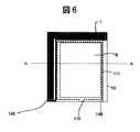
図6は本実施例のシールパターン例を説明する平面図であり、前記図4は図5のA−A’線に沿った断面に相当する。基板10上には表示領域であるマトリクス表示部8と太陽電池1が配置されており、これらを封止するシールとして、太陽電池シール145、液晶シール144を図6のように配置する。TFTを基板10上に形成し、太陽電池1を形成後、対向基板171とを貼り合わせた後に液晶を真空封入法により封入する。このときに封入口170には太陽電池1は配置されておらず、かつ端子部(図6の右辺)の無い辺に設けた。この位置に封入口170を配置することにより太陽電池の設置面積を減らすことなく、また端子部の設置領域を有効に使用でき、高い発電電力が得られると共に、端子部に設ける端子の接続ピッチを大きくとることが出来る利点がある。言い換えれば、封止口170を設ける辺は対向基板171と、基板1 0との端部がほぼ揃っている図6に示した辺とするのが好適であり、少なくとも太陽電池1が形成されていない辺に配置することが必須である。有機の太陽電池は溶剤に溶融するため液晶と接する事が無いように配置することが必要である。したがって、図6に示すように液晶シールの外側に配置することが重要である。
【0028】
また、図1に示すように太陽電池1の配置については、操作のためのスイッチ9と離れた位置に配置する。太陽電池1の近傍もしくは太陽電池に重なるように操作スイッチ9を配置すると画面の操作をする場合に太陽電池を遮り、発電能力を著しく低下させる原因となる。したがって、太陽電池1と操作スイッチ9は離れた位置に配置することが電力供給の効率向上の効果に於いて有用である。
【0029】
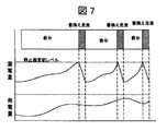
次に、表示部の駆動制御について説明する。図7は表示画面の書換えと電源部の蓄電量の説明図である。太陽電池の発電量は一定ではなく、外光量に応じて変動しており、蓄電素子に蓄えられる電力あるいは電荷量は時間とともに次第に増加するが増加率は一様ではない。したがって、ここでは画面1面分を書き換えるのに必要な電力を電圧に換算し、静止画更新レベルの電圧に達したことを検出して書換え動作を開始する。書き換え走査期間中は電力が消費されるので、発電量が走査回路動作時の消費電力以下の場合には図示したように、蓄電量が低下する。書換え期間走査後に再び太陽電池からの電力により再び蓄電量が増加する。このように画面書換え走査を蓄電量がある電力に達するごとに間欠動作する事により消費電力を極限にまで低減した駆動が可能となる。
【0030】
また、表示の書換えの制御に関しては、表示切替スイッチ9の操作と、蓄電量とも関係付けてさらに低電力化を実現した。図8は表示の書換えの制御に関する表示切替スイッチの操作と蓄電量との関係付けの説明図である。図8において、使用者により表示の切り替えを要求するスイッチが押下されると、1画面の書換えに必要な電力が蓄電できているかを検知する電力検出信号の有無を検知し、信号が有効であれば表示の書換え動作を実行する。しかし、もし電力が不足している場合には書き換えないように制御する。これにより、表示の書換えはスイッチ9を押下しない間は表示の書換え電力を節約し、押下されても電力が足りない場合は書換えを止めて表示を更新しないで維持するように駆動して電力を低減するように制御され、低電力化が実現できる。
【0031】
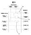
図9は表示において静止画の書換えに加えて動画を表示させる場合の制御論理の説明図である。静止画の書換えに加えて動画を表示させる場合には図9に示す制御論理により制御する。蓄電素子の蓄電電力量を図3に示したような回路構成により静止画表示レベル信号A、静止画更新レベル信号B、動画駆動レベル信号Cの3種類のレベルを検出した論理信号を与える。また、画像の書換え要求を示す論理信号として、静止画の画面書換えおよび動画表示の要求信号を当て、図9に示したような論理演算回路51a、51b、51 cにより駆動制御信号を得る。静止画表示レベルを下回る場合には3種類のレベル信号はいずれも無効となり液晶表示を停止する。静止画表示レベル信号Aが有効になると液晶の表示駆動動作信号を出力し、画素部表示に必要な電力を供給する。静止画表示レベルと静止画画面書換えレベルの間であれば部分書換動作をさせることができる。ほぼ表示部分のみで必要な部分を書き換えて最小限の情報を新しくできる。
【0032】
静止画更新レベル信号Bが有効で、かつ画面書換え要求信号が有効な場合には表示書換え操作信号は有効となり、表示を書き換えるように表示回路の走査駆動を1画面分のみ実行する。また動画の要求信号が来ている場合には低速の動画を表示する。この場合には書換え電力が得られるごとに画面が変わるのでゆっくりとした動画表示が得られる。動画駆動レベルの信号Cが有効な場合には、静止画の書換え要求信号がきている場合には静止画を繰り返し表示し、動画要求信号が来ている場合には動画を連続して書き換える。
【0033】
図10は上記した本実施例における段階的な表示モードの構成をまとめた説明図である。図10において、蓄電電力量の増加に伴い、表示駆動、画面書換え駆動、静止画の連続書換え駆動、および動画の間欠駆動から、次第に書換えのインターバルが短くなり、通常の動画駆動となるように制御する。このように駆動することにより、電力の供給量が大幅に変化しても、表示モードを切り換えて低電力でも表示することができる。従来の駆動方式では、走査モードを電力量に連動して切り替えるような制御をしていないので、発電量が連続書換えレベルを下回ると表示が停止してしまう。静止画表示レベルと静止画画面書換えレベルの間であれば部分書換動作をさせることができる。ほぼ表示部分のみで必要な部分を書き換えて最小限の情報を新しくできる。
【0034】
図11は本発明の表示装置における画素回路の説明図である。画素には表示電極85、対向基板に形成した対向電極86の間に狭持した液晶を駆動する。表示電極85は反射型液晶表示モードで駆動するので金属薄膜で形成する。画素の表示データは信号配線82を介して画素に入力し、走査配線81により線順次の選択信号である走査信号を供給する。走査配線と信号配線に接続した画素の薄膜トランジスタ(TFT)83が走査信号により選択されると表示データを画素内のメモリ回路84に取り込む。メモリ回路84はいわゆるスタティックRAMの回路構成を用いている。メモリ回路84の出力端子99は2つ有り、記憶の状態に応じて互いに逆の極性の信号を出力する。
【0035】
2つの駆動用のTFT87は表示電極85に接続されている。オフ電圧配線88もしくはオン電圧配線89に接続されており、記憶状態に応じてどちらかの駆動用TFTがオンするので表示電極85にはオフ電圧配線88もしくはオン電圧配線89電圧を選択的に印加することができる。オフ電圧配線88、オン電圧配線89は相互に接続され、オフ電圧配線88には0V、オン電圧配線89には液晶を駆動する閾値以上の交流の液晶駆動電圧が印加されている。また、対向電極86には常に0Vが印加されている。これにより、画素ではメモリ回路84に記憶したデータにより表示電極85には0Vもしくは液晶駆動電圧が印加するように駆動でき、点灯もしくは非点灯の2つの状態を駆動できる。
【0036】
図12は表示部の周囲に配置した駆動回路の構成を説明する回路図である。駆動回路は走査開始信号136とクロック1配線135a、クロック2配線135bにより駆動されるインバータ回路134を組み合わせたシフトレジスタ133と、データを取り込むサンプリングラッチ137、ラインラッチ138およびデータを表示部のデータ電圧に変換するデータスイッチ139から構成される。データは走査開始信号136によりシフトレジスタの動作を開始し、これに同期してデータ線から各画素のデータが送られ、サンプリングラッチ137に取り込まれる。
【0037】
1ライン分のデータがそろった時点でラッチ信号を入力しラインラッチ138にデータを転送する。表示部を駆動する出力140は各々表示部のデータ配線に接続されている。なお、クロックおよび走査開始信号の入力側には各々スイッチ131、132が設けられており、画像書換えが可能である場合にオン状態となるように制御し、表示書換えを実行するように制御する。
【0038】
次に、本発明の第2実施例について説明する。前記実施例は表示部に液晶ディスプレイパネルを用いたものであるが、本実施例は電気泳動ディスプレイパネルを用いている。電気泳動ディスプレイパネルは、表示電極および対向電極の間に絶縁性の媒質に帯電した微小粒を分散させ、外部からの電界により微小粒を表示電極もしくは対向電極に移動、凝集させる事により表示する表示方式である。表示を切り換えた後は表示を書き換えるまで外部からの電界が無くても長時間表示を維持する事ができるので液晶ディスプレイパネルよりもより低電力で駆動できる利点がある。この表示装置の構成は、その素子構造が2枚の基板間に狭持した表示素子を用いることなど、概略第1実施例と同じである。しかし、マトリクス表示部を構成する画素回路が異なる。
【0039】
図13は本発明の第2実施例にかかる電気泳動ディスプレイパネルの画素構成の説明図である。図13において、走査配線81、データ配線82、画素の薄膜トランジスタ(TFT)83は図11と同じであるが、データ電圧は保持コンデンサ91に蓄えるとともにCMOSTFT94a、94bにより構成したインバータを介して表示電極95に接続する。インバーターには2本の電源配線97a、97bにより駆動される。ここでは、電源配線の1本と、保持コンデンサ91の共通電極を共通の配線に接続して配線本数を減らしている。この構成において、書き込まれたデータ電圧はインバータで反転増幅されて、電気泳動素子96を駆動する。書き込みは走査信号が選択する短時間であり、電気泳動素子92の応答は微小粒の移動を伴うため応答が終わらない。保持コンデンサ91とインバータにより選択終了後も画素内に蓄えている保持期間にわたり素子を駆動するので、電気泳動素子92の応答が遅くても十分な時間の電圧を印加して素子を駆動でき、電気泳動素子92の応答時間を補う利点がある。
【0040】
図14は本発明の第2実施例の画素回路の変形例の説明図であり、図13に示した構成に保持インバータ111と帰還配線112を追加したものである。保持インバーター111はインバータ前段のと組み合わせてデータ保持回路を構成するので書き換えたデータは電源が供給されている期間中は書換え動作を行わなくてもデータを保持できる利点がある。なお、液晶ディスプレイパネルとして透過型や半透過反射型を用いた表示装置、あるいは液晶ディスプレイパネルの背面に、所謂バックライトを備えた液晶表示装置にも同様に適用できることは言うまでもない。
【0041】
図15は本発明の第2実施例の画素回路の他の変形例の説明図であり、画素回路をサンプリング用のTFT121、補助容量122で構成したものである。画素に書き込んだデータ電圧は選択終了後にわたり微小粒の移動があるため時間とともに電気泳動素子の電圧が低下してしまうのを補うために、補助容量122を電気泳動素子92と並列に接続して電圧変動を押さえるようにした。サンプリングTFT121は保持特性を得るためダブルゲートTFTを用いるのが好適である。このような画素回路を用いて構成した表示装置の駆動は表示の維持には電力が不要なので電力制御も異なる。
【0042】
図16は本発明の第2実施例における蓄電電力量と駆動モードとの関係の説明図である。図16に示すように、静止画の書換え電力以下の発電量では表示の維持のレベルが不在であり、液晶よりも低い電力で駆動することができる。液晶ディスプレイパネルを用いたものでは、図11で説明したように液晶駆動電圧が常時必要であったのに対し、電気泳動ディスプレイパネルを用いたものでは表示維持の電力が不要であるためである。したがって、図10での表示消灯、表示駆動の領域は図16には存在しないことでも明らかである。
【0043】
【発明の効果】
以上説明したように、本発明によれば、極めて消費電力が低く、供給電力に応じて画像の書換え速度、画素数を可変とした表示装置を提供することができる。そして、本発明の表示装置によれば、発電電力が環境によって大きく変化する太陽電池を用いても、ようやく文字が判読できるような環境下でも表示が可能であり、スイッチ操作により室内光での静止画を鮮明に表示し、明るい場所と暗い場所との画面表示をスイッチ操作によってスムーズに切り替えを行うことが可能となる。
【0044】
さらに、明るい場所では表示内容を次々に変化させ、あるいは動画のような情報量が豊富な表示を提供できる表示装置を電源配線の接続あるいは充電に煩わされること無く使用できる携帯表示装置を構成することが容易である。また、本発明では、表示装置を点灯したまま放置しても電池切れが無いにもかかわらず、重量が大きくかさばる2次電池の容量を従来よりも著しく少なくすることができ、表示装置を薄型化、軽量化することができる。
【0045】
本発明によれば、搭載する電力バッファの容量が低くても電力が自立し、電池寿命のない携帯性が優れた表示装置を提供することができる。
【0046】
そして、本発明による表示装置は電源の管理が不要であり、かつ環境光が豊富である場合には、表示容量、画質、情報量が豊富に成る特徴を有しており、人間の視角能力に適応した表示制御がなされたリーズナブルな表示装置を提供することができる。
【図面の簡単な説明】
【図1】本発明の第1実施例にかかる表示装置のシステム構成図である。
【図2】本発明の第1実施例にかかる表示装置の外観図である。
【図3】本発明の第1実施例にかかる表示装置おける電源部の構成図である。
【図4】本発明の第1実施例にかかる表示装置の基板の構造例を説明する模式断面図である。
【図5】本発明の第1実施例の変形例における表示装置の基板の構造を説明する模式断面図である。
【図6】本発明の第1実施例のシールパターン例を説明する平面図である。
【図7】本発明の第1実施例における表示画面の書換えと電源部の蓄電量の説明図である。
【図8】本発明の第1実施例における表示の書換えの制御に関する表示切替スイッチの操作と蓄電量との関係付けの説明図である。
【図9】本発明の第1実施例の表示において静止画の書換えに加えて動画を表示させる場合の制御論理の説明図である。
【図10】本発明の第1実施例の表示における段階的な表示モードの構成をまとめた説明図である。
【図11】本発明の表示装置における画素回路の説明図である。
【図12】本発明の表示装置における表示部の周囲に配置した駆動回路の構成を説明する回路図である。
【図13】本発明の第2実施例にかかる電気泳動ディスプレイパネルの画素構成の説明図である。
【図14】本発明の第2実施例の画素回路の変形例の説明図である。
【図15】本発明の第2実施例の画素回路の他の変形例の説明図である。
【図16】本発明の第2実施例における蓄電電力量と駆動モードとの関係の説明図である。
【符号の説明】
1・・・・太陽電池、 1・・・・蓄電素子(蓄電部)、3・・・・蓄電検出回路、4・・・・駆動回路、5・・・・入力端子、6・・・・データバッファ、7・・・・制御回路、8・・・・マトリクス表示部、9・・・・スイッチ、10・・・・ガラス基板、21・・・・基板、22・・・・太陽電池22、 23・・・・表示領域、26・・・・駆動回路LSI、24・・・・データ入出力LSI、28・・・・太陽、32・・・・基準電圧回路、33・・・・電源33、34a,34b,34c・・・・コンパレータ、51a,51b,51 c・・・・論理演算回路、81・・・・走査配線、82・・・・信号配線、83・・・・画素TFT、84・・・・メモリ回路、85・・・・表示電極、86・・・・対向電極、87・・・・駆動用TFT、88・・・・オフ電圧配線、89・・・・オン電圧配線、99・・・・メモリ回路の出力端子、91・・・・保持コンデンサ、94a,94b・・・・CMOSTFT、95・・・・表示電極、96・・・・電気泳動素子、97a,97b・・・・電源配線、111・・・・保持インバータ、112・・・・帰還配線、121・・・・サンプリングTFT、122・・・・補助容量、142・・・・ガラス基板、144・・・・液晶シール、145・・・・太陽電池シール、146・・・・ポリシリコンTFT、147・・・・薄膜太陽電池、149・・・・Al電極、151・・・・反射防止膜、166・・・・島状シリコン、167・・・・ゲート絶縁膜、168・・・・ゲート電極、165・・・・配線層、31・・・・MOSコンデンサ、190・・・・有機半導体層、161・・・・アモルファスシリコン層、162・・・・透明電極、163・・・・パッシベーション層、171・・・・対向基板、170・・・・封入口。[0001]
[Industrial application fields]
The present invention relates to a display device driven with low power, and more particularly to a low power electronic display device combining a solar cell and a liquid crystal and requiring no charging, and a control method thereof.
[0002]
[Prior art]
Many display devices having a power source for supplying power using a solar cell or the like have been proposed so far. For example, “
[0003]
In a display device that uses a solar cell as a power source, the supplied power varies greatly depending on the amount of light applied to the solar cell. For this reason, when power is insufficient, display drive cannot be performed and the display disappears. Therefore, by combining a solar battery and a rechargeable secondary battery, auxiliary power means for supplementing power is generally provided in parallel so that display driving can be performed even when the output of the solar battery stops. there were. In addition, “
[0004]
[Patent Document 1]
JP 2001-184033 A
[Patent Document 2]
JP-A-5-73117
[Patent Document 3]
JP 2000-112441 A
[Non-Patent Document 1]
April 10, 2002, published by the Japan Society of Applied Physics, “Applied Physics” Vol. 71, No. 4 (pp. 425-428).
[0005]
[Problems to be solved by the invention]
As described above, in a conventional display device in which a solar cell is mounted as a power source, in addition to the solar cell, a large-capacity secondary battery that covers power required for display driving is generally mounted. . Therefore, the weight of the device is heavy and the thickness is increased. In addition, to charge the secondary battery, it is necessary to connect the fixed power supply and the display device with an electric wire, and portable devices cannot be carried during the charging period, so the usability is limited. Further, in a display device including an auxiliary lighting device such as a backlight or a front light, when the ambient illuminance (brightness of external light) is strong, the illuminance is supplied from the solar cell. When it is low, the display mode is generally switched so as to control the power supply of the backlight supplied from the secondary battery. And in the display which supplies electric power from a secondary battery, it is common to reduce the brightness of a display screen in order to suppress consumption of a battery. As a result, the display image quality is greatly degraded. Conventionally, sufficient consideration has not been given to means for solving the above-described problems.
[0006]
An object of the present invention is to provide a display device that is equipped with a solar cell and a power storage element that sustainably stores electric power, has a low power driving mode, makes electric power independent, and does not require charging and power supply wiring.
[0007]
[Means for Solving the Problems]
In order to achieve the above object, the present invention is characterized by having the following configuration. That is, a typical configuration of the present invention includes a power supply unit that supplies power, a display unit that displays an image, and a data input circuit and a control circuit that input display data corresponding to the image,
The power supply unit is necessary for rewriting one screen and a power source whose power supply capability changes with time, or switches between a plurality of different power supply capacities, or whose average generated power is lower than the average power required for rewriting one screen. A power storage unit having a power storage capacity that holds power larger than average power, and a power storage detection circuit that detects a power storage amount of the power storage unit,
The power source is connected to the display unit via the power storage unit,
The display unit includes a matrix display region in which a large number of pixels having an optical modulation function capable of changing luminance, reflectance, transmittance, and color by voltage or current are arranged in a matrix, and a sequential circuit that drives the matrix display region. It consists of a drive circuit,
The input of the data input circuit is connected to a data input terminal, and the output is connected to the drive circuit of the display unit,
The pixel has a pixel memory for holding display data, and is driven by a pixel rewriting period for rewriting display contents of the display unit and a pixel holding period for holding display contents, and the control circuit is at least a screen from the storage detection circuit The screen of the display unit is rewritten by controlling the drive circuit so as to rewrite the display content of the display unit by outputting a power storage detection signal that detects the amount of power storage greater than the average power required for rewriting Configured.
[0008]
Further, according to the present invention, a power storage unit that stores power necessary for display driving is provided between the solar cell and the display unit using a secondary battery or a capacitor, and power is supplied to the display unit via the power storage element. Connect a storage detection circuit to the power storage unit, monitor the amount of stored power and generated power, and store the power required for driving, power that can be scanned and rewritten, and power that can be rewritten continuously. A power storage level signal is generated by the power storage detection circuit.
[0009]
Further, according to the present invention, a pixel memory that stores display contents for each pixel is provided in the display unit, and the contents of the pixel memory are rewritten by line-sequential scanning driving. The pixel driving circuit that drives the pixels has a memory function of the pixels. The display is configured to change the transmittance and reflectance according to the stored display contents.
[0010]
In addition, the present invention supports a display rewrite instruction using a push button switch, a mouse, a pen, or the like for instructing to change a display mode of still image display, still image update, and moving image display, and a rewritable charge level signal is effective. In some cases, a control circuit is provided for controlling the scanning drive so as to execute a rewriting operation for rewriting the display.
[0011]
In addition, the present invention supports a display rewriting instruction by a push button switch, mouse, pen, or the like in which the control circuit instructs to change the display, and the display is continuously performed when the signal of the storage level that can be continuously rewritten is valid. The scanning drive is controlled so as to execute the rewriting operation to be rewritten.
[0012]
The display device of the present invention configured as described above performs a display operation in the following manner. (A) A solar cell converts incident light energy into electric power. The power storage unit stores the generated power. The electricity storage detection circuit monitors the amount of electricity stored in the electricity storage unit, and it has a plurality of electricity storage levels indicating that the electric power required for driving, the electric power that can be scanned and rewritten display content, and the electric power that can be continuously rewritten are stored. Generate a signal. (B) The pixel memory function stores display contents for each pixel by line-sequential scanning drive, and the pixel drive circuit displays the display by changing the transmittance and reflectance according to the display contents stored by the pixel memory function. (C) The control drive circuit detects a display rewrite instruction by a push button switch, a mouse, a pen, or the like that instructs a display change, and detects which of a plurality of charge level signals is valid, and can be rewritten. When the power level signal is valid, the scanning drive is controlled to execute the rewrite operation to rewrite the display, and when the rewriteable power level signal is valid, the display is rewritten continuously. The scanning drive is controlled to execute the above.
[0013]
Note that the present invention is not limited to the above-described configuration and the configuration disclosed in the embodiments described later, and it goes without saying that various modifications can be made without departing from the technical idea of the present invention. .
[0014]
DETAILED DESCRIPTION OF THE INVENTION
Hereinafter, the liquid crystal display device of the present invention will be described in detail with reference to the drawings of the embodiments. FIG. 1 is a system configuration diagram of a display device according to a first embodiment of the present invention. The display device of this embodiment is a reflective liquid crystal display panel. The liquid crystal display panel has a matrix display unit 8 and supplies power to the
[0015]
The display device of this embodiment is an active matrix system using an active element such as a thin film transistor for pixel selection of the matrix display unit 8. In the following description, a liquid crystal display panel (TFT-LCD) using a thin film transistor (TFT) as an active element will be described as an example. The TFT-LCD performs display in a reflective display mode, and the
[0016]
FIG. 2 is an external view of the display device of this embodiment. The display device is composed of two
[0017]
FIG. 3 is a configuration diagram of a power supply unit in the display device of this embodiment. An organic thin-film solar cell was used as the solar cell 22 (the power supply unit for the
[0018]
Both the
[0019]
The power storage detection circuit for measuring the amount of power stored in the power storage element in this way is constituted by a
[0020]
In addition, as a structure of a solar cell, the thin film solar cell and the solar cell using organic thin film semiconductors, such as a conjugated polymer and a dye sensitizing system, are used for amorphous silicon and polycrystal silicon (polysilicon: poly-Si). I can do it. Further, as shown in FIG. 2, a
[0021]
FIG. 4 is a schematic cross-sectional view for explaining a structural example of a substrate of the display device of this embodiment. A
[0022]
The
[0023]
Next, PEDOT, P3DOT, POPT, MDMO-PPVMEH-PPV, which is a π-conjugated polymer that serves as an electron donor as a p-type semiconductor, is dissolved in a solvent such as toluene or xylene having a polarity different from that of the underlayer, and spin coated. The film is laminated and dried. The film thickness of the p-type layer is 50 nm after drying. Finally, ITO is formed to a thickness of 70 nm as the
[0024]
With this configuration, one
[0025]
As a solar cell, a pentacene vapor-deposited thin film, a successful transport layer such as OMeTAD may be used as a low molecular conductive organic semiconductor, and an amorphous Si film may be formed by PECVD as an inorganic semiconductor thin film. good. In any case, by forming the thin film solar cell after the formation of the polysilicon TFT by a low temperature process lower than the process temperature of the polysilicon TFT, the deterioration of the characteristics of the polysilicon TFT can be prevented, and the display portion and the solar cell can be formed on the same substrate. .
[0026]
FIG. 5 is a schematic cross-sectional view for explaining the structure of the substrate of the display device in a modification of the first embodiment of the present invention. In the case where amorphous silicon is used for the solar cell portion, a
[0027]
FIG. 6 is a plan view for explaining an example of a seal pattern of this embodiment, and FIG. 4 corresponds to a cross section taken along the line AA ′ of FIG. The matrix display unit 8 and the
[0028]
Further, as shown in FIG. 1, the
[0029]
Next, drive control of the display unit will be described. FIG. 7 is an explanatory diagram of rewriting the display screen and the amount of electricity stored in the power supply unit. The amount of power generated by the solar cell is not constant and fluctuates according to the amount of external light. The amount of power or charge stored in the power storage element gradually increases with time, but the rate of increase is not uniform. Therefore, here, the power required to rewrite one screen portion is converted into a voltage, and the rewriting operation is started by detecting that the voltage has reached the still image update level. Since power is consumed during the rewrite scanning period, as shown in the figure, the amount of stored electricity decreases when the power generation amount is equal to or lower than the power consumption during the scanning circuit operation. After the rewrite period scanning, the amount of stored electricity again increases due to the power from the solar cell. In this way, the screen rewriting scan is intermittently operated every time the amount of stored electricity reaches a certain amount of power, thereby enabling driving with reduced power consumption to the limit.
[0030]
Further, regarding the display rewriting control, the operation of the display change-over switch 9 and the amount of stored electricity are related to each other to further reduce the power. FIG. 8 is an explanatory diagram of the relationship between the operation of the display changeover switch and the amount of stored electricity related to display rewriting control. In FIG. 8, when a user presses a switch requesting display switching, the presence or absence of a power detection signal for detecting whether or not the power necessary for rewriting one screen can be stored is detected, and the signal is valid. Display rewrite operation is executed. However, if power is insufficient, control is performed so as not to rewrite. As a result, the display rewriting saves display rewriting power while the switch 9 is not pressed, and if the power is not enough even when the switch 9 is pressed, the rewriting is stopped and the display is renewed so that the display is maintained without being updated. It is controlled to reduce, and low power can be realized.
[0031]
FIG. 9 is an explanatory diagram of the control logic when displaying a moving image in addition to rewriting a still image. When displaying a moving image in addition to rewriting of a still image, control is performed by the control logic shown in FIG. A logic signal in which three types of levels of a still image display level signal A, a still image update level signal B, and a moving image drive level signal C are detected is applied to the stored electric energy of the storage element by a circuit configuration as shown in FIG. Further, a request signal for still image screen rewriting and moving image display is applied as a logical signal indicating an image rewriting request, and a drive control signal is obtained by
[0032]
When the still image update level signal B is valid and the screen rewrite request signal is valid, the display rewrite operation signal is valid, and the scanning drive of the display circuit is executed for one screen so as to rewrite the display. When a video request signal is received, a low-speed video is displayed. In this case, since the screen changes every time rewriting power is obtained, a slow moving image display can be obtained. When the moving image driving level signal C is valid, the still image is repeatedly displayed when the still image rewrite request signal is received, and the moving image is continuously rewritten when the moving image request signal is received.
[0033]
FIG. 10 is an explanatory diagram summarizing the structure of the stepwise display mode in the above-described embodiment. In FIG. 10, control is performed so that the normal rewriting interval is gradually shortened from the display driving, the screen rewriting driving, the still image continuous rewriting driving, and the moving image intermittent driving with the increase in the amount of stored power. To do. By driving in this way, even if the amount of power supply changes significantly, the display mode can be switched to display even at low power. In the conventional driving method, since the scanning mode is not controlled to be switched in conjunction with the power amount, the display is stopped when the power generation amount falls below the continuous rewriting level. A partial rewrite operation can be performed between the still image display level and the still image screen rewrite level. The necessary information can be rewritten with almost only the display part, and the minimum information can be renewed.
[0034]
FIG. 11 is an explanatory diagram of a pixel circuit in the display device of the present invention. The pixel is driven by liquid crystal sandwiched between the display electrode 85 and the counter electrode 86 formed on the counter substrate. Since the display electrode 85 is driven in the reflective liquid crystal display mode, it is formed of a metal thin film. Display data of the pixel is input to the pixel through the
[0035]
The two driving
[0036]
FIG. 12 is a circuit diagram illustrating a configuration of a drive circuit arranged around the display unit. The drive circuit includes a
[0037]
When the data for one line is ready, a latch signal is input and the data is transferred to the
[0038]
Next, a second embodiment of the present invention will be described. In the above embodiment, a liquid crystal display panel is used for the display unit. In this embodiment, an electrophoretic display panel is used. An electrophoretic display panel is a display that disperses fine particles charged in an insulating medium between display electrodes and a counter electrode, and moves and aggregates the fine particles to the display electrode or the counter electrode by an external electric field. It is a method. After the display is switched, the display can be maintained for a long time without an external electric field until the display is rewritten. Therefore, there is an advantage that the display can be driven with lower power than the liquid crystal display panel. The configuration of this display device is substantially the same as that of the first embodiment, such as using a display element whose element structure is held between two substrates. However, pixel circuits constituting the matrix display unit are different.
[0039]
FIG. 13 is an explanatory diagram of the pixel configuration of the electrophoretic display panel according to the second embodiment of the present invention. In FIG. 13, the
[0040]
FIG. 14 is an explanatory diagram of a modification of the pixel circuit according to the second embodiment of the present invention, in which a holding
[0041]
FIG. 15 is an explanatory diagram of another modification of the pixel circuit according to the second embodiment of the present invention. The pixel circuit includes a
[0042]
FIG. 16 is an explanatory diagram of the relationship between the amount of stored power and the drive mode in the second embodiment of the present invention. As shown in FIG. 16, when the power generation amount is less than or equal to the rewriting power of a still image, the level of display maintenance is absent, and the display can be driven with lower power than the liquid crystal. This is because a liquid crystal display panel always requires a liquid crystal driving voltage as described with reference to FIG. 11, whereas an electrophoretic display panel does not require display maintaining power. Therefore, it is clear that the display extinction and display drive regions in FIG. 10 do not exist in FIG.
[0043]
【The invention's effect】
As described above, according to the present invention, it is possible to provide a display device that has extremely low power consumption and can change the image rewriting speed and the number of pixels according to the supplied power. According to the display device of the present invention, even when using a solar cell whose generated power greatly changes depending on the environment, it can be displayed even in an environment where the characters can be finally read, and it can be stopped in room light by a switch operation. It is possible to display the image clearly and smoothly switch the screen display between the bright place and the dark place by the switch operation.
[0044]
Furthermore, a portable display device that can change a display content one after another in a bright place or can use a display device that can provide a rich display of information such as a moving image without being troubled by connection of a power supply wiring or charging. Is easy. Further, according to the present invention, the capacity of the secondary battery, which is heavy and bulky, can be remarkably reduced compared with the conventional case even though the display device is left on and the battery is not exhausted. Can be lighter.
[0045]
According to the present invention, it is possible to provide a display device that is self-supporting even when the capacity of a power buffer to be mounted is low, and has excellent portability without battery life.
[0046]
The display device according to the present invention does not require power management, and has a feature that the display capacity, image quality, and information amount are abundant when the environment light is abundant. A reasonable display device with adaptive display control can be provided.
[Brief description of the drawings]
FIG. 1 is a system configuration diagram of a display device according to a first embodiment of the present invention.
FIG. 2 is an external view of a display device according to a first embodiment of the present invention.
FIG. 3 is a configuration diagram of a power supply unit in the display device according to the first embodiment of the present invention.
FIG. 4 is a schematic cross-sectional view for explaining a structural example of a substrate of the display device according to the first example of the present invention.
FIG. 5 is a schematic cross-sectional view illustrating the structure of a substrate of a display device according to a modification of the first embodiment of the present invention.
FIG. 6 is a plan view for explaining an example of a seal pattern according to the first embodiment of the present invention.
FIG. 7 is an explanatory diagram of display screen rewriting and the amount of power stored in the power supply unit in the first embodiment of the present invention.
FIG. 8 is an explanatory diagram of the relationship between the operation of the display changeover switch and the amount of stored electricity related to display rewriting control in the first embodiment of the present invention.
FIG. 9 is an explanatory diagram of control logic in a case where a moving image is displayed in addition to the rewriting of a still image in the display according to the first embodiment of this invention.
FIG. 10 is an explanatory diagram summarizing the structure of the stepwise display mode in the display of the first embodiment of the present invention.
FIG. 11 is an explanatory diagram of a pixel circuit in a display device of the present invention.
FIG. 12 is a circuit diagram illustrating a configuration of a drive circuit arranged around a display unit in a display device of the present invention.
FIG. 13 is an explanatory diagram of a pixel configuration of an electrophoretic display panel according to a second embodiment of the present invention.
FIG. 14 is an explanatory diagram of a modification of the pixel circuit according to the second embodiment of the present invention.
FIG. 15 is an explanatory diagram of another modification of the pixel circuit according to the second embodiment of the present invention.
FIG. 16 is an explanatory diagram of the relationship between the amount of stored power and the drive mode in the second embodiment of the present invention.
[Explanation of symbols]
DESCRIPTION OF
Claims (6)
Translated fromJapanese前記電源部は、供給能力が時間とともに変化する、または平均発生電力が1画面の書換えに必要な平均電力よりも低い電源と、1画面の書換えに必要な平均電力よりも大きな電力を保持する蓄電容量を有する蓄電部と、前記蓄電部の蓄電量を検出する蓄電検出回路からなり、
前記電源は前記蓄電部を介して前記表示部に接続されており、
前記表示部は、電圧もしくは電流により輝度、反射率、透過率および色を変化できる光学変調機能を有する画素を多数マトリクス状に配列したマトリクス表示領域と、前記マトリクス表示領域を駆動する順序回路を含む駆動回路から構成されており、
前記画素は表示データを保持する画素メモリを有し、前記表示部の画素メモリの表示内容を書き換える画素書換え期間と表示内容を保持する画素保持期間により駆動されており、
前記制御回路は、前記蓄電検出回路が少なくとも画面の書換えに必要な平均電力以上の蓄電量を検出した蓄電検出信号を出力した場合に画素表示内容を書き換えることにより静止画面を書き換えるように駆動回路を制御し、前記蓄電検出回路が前記画面を連続して書換えるのに必要な平均電力以上の蓄電量を検出した蓄電検出信号を出力した場合に連続して前記画面を書き換えることにより前記表示部の画素メモリの表示内容を繰り返し書き換えるように前記駆動回路を制御して前記表示部に動画を表示することを特徴とする表示装置。A power supply unit that supplies power, a display unit that displays an image, a data input circuit that inputs display data corresponding to an image displayed on the display unit, a data buffer that stores the input display data, and display contents of the display unit A display device having rewrite input means and a control circuit for requesting a change in
The power supply unit stores a power supply whose supply capacity changes with time or whose average generated power is lower than the average power necessary for rewriting one screen and power larger than the average power necessary for rewriting one screen. A power storage unit having a capacity, and a power storage detection circuit for detecting a power storage amount of the power storage unit,
The power source is connected to the display unit via the power storage unit,
The display unit includes a matrix display region in which a large number of pixels having an optical modulation function capable of changing luminance, reflectance, transmittance, and color by voltage or current are arranged in a matrix, and a sequential circuit that drives the matrix display region. It consists of a drive circuit,
The pixel has a pixel memory for holding display data, and is driven by a pixel rewriting period for rewriting display contents of the pixel memory of the display unit and a pixel holding period for holding display contents,
The control circuit sets a drive circuit to rewrite a static screen by rewriting the pixel display content when the power storage detection circuit outputs a power storage detection signal that detects a power storage amount that is at least equal to the average power required for screen rewriting. Control, and when the power storage detection circuit outputs a power storage detection signal that detects a power storage amount that is equal to or higher than the average power required to continuously rewrite the screen, the screen of the display unit is rewritten. A display device that controls the drive circuit to repeatedly rewrite display contents of a pixel memory and displays a moving image on the display unit.
前記電源部は供給能力が時間とともに変化する、または平均発生電力が1画面の書換えに必要な平均電力よりも低い電源と、1画面の書換えに必要な平均電力よりも大きな電力を保持する蓄電容量を有する蓄電部と、前記蓄電部の蓄電量を検出する蓄電検出回路からなり、
前記電源は前記蓄電部を介して前記表示部に接続されており、
前記表示部は、電圧もしくは電流により輝度、反射率、透過率および色を変化できる光学変調機能を有する画素を多数マトリクス状に配列したマトリクス表示領域と、マトリクス表示領域を駆動する順序回路を含む駆動回路から構成されており、
前記蓄電検出回路から少なくとも前記表示部の画面の書換えに必要な平均電力以下の蓄電量を検出した蓄電検出信号を出力した場合は前記駆動回路を停止させることにより前記表示部の画面の書換えを停止し、
前記蓄電検出回路から少なくとも前記表示部の画面の書換えに必要な平均電力以上の蓄電量を検出した蓄電検出信号が出力された場合に画素表示内容を書き換えることにより前記画面を書き換えるよう前記駆動回路を制御して静止画面を書き換え、
前記制御回路は、前記蓄電検出回路が画面を連続して書換えるのに必要な平均電力以上の蓄電量を検出した蓄電検出信号を検出した場合には連続して画素表示内容を書き換えて前記表示部の画面を書き換えるように前記駆動回路を制御して動画像を表示することを特徴とする表示装置。A power supply unit that supplies power, a display unit that displays an image, a rewrite input unit that requests a change in display content of the display unit, and a data input circuit that inputs display data corresponding to an image displayed on the display unit A display device having a data buffer and a control circuit for storing the display data inputted,
The power supply unit has a power supply capacity whose supply capability changes with time or whose average generated power is lower than the average power required for rewriting one screen and a power storage capacity that holds a larger power than the average power required for rewriting one screen And a power storage detection circuit for detecting a power storage amount of the power storage unit,
The power source is connected to the display unit via the power storage unit,
The display unit includes a matrix display region in which a large number of pixels having an optical modulation function capable of changing luminance, reflectance, transmittance, and color by voltage or current are arranged in a matrix, and a driving circuit including a sequential circuit that drives the matrix display region. Consists of a circuit,
When the power storage detection signal is output from the power storage detection circuit to detect a power storage amount that is at least less than the average power required for rewriting the screen of the display unit, rewriting of the screen of the display unit is stopped by stopping the drive circuit And
The drive circuit is configured to rewrite the screen by rewriting the pixel display content when the power storage detection signal is output from the power storage detection circuit to detect a power storage amount that is at least equal to the average power required for rewriting the screen of the display unit. Control and rewrite the still screen,
The control circuit continuously rewrites the pixel display content when the storage detection signal is detected that detects a storage amount greater than the average power necessary for the storage detection circuit to continuously rewrite the screen. A display device that displays a moving image by controlling the drive circuit so as to rewrite a screen of a part.
Priority Applications (6)
| Application Number | Priority Date | Filing Date | Title |
|---|---|---|---|
| JP2002359618AJP3873149B2 (en) | 2002-12-11 | 2002-12-11 | Display device |
| TW092110186ATWI266267B (en) | 2002-12-11 | 2003-04-30 | Display device |
| CNB031362966ACN1317685C (en) | 2002-12-11 | 2003-05-21 | display device |
| KR1020030057172AKR20040051484A (en) | 2002-12-11 | 2003-08-19 | Display device |
| US10/648,789US7319465B2 (en) | 2002-12-11 | 2003-08-27 | Low-power driven display device |
| EP03019702AEP1429310A3 (en) | 2002-12-11 | 2003-08-28 | Low-power driven display device |
Applications Claiming Priority (1)
| Application Number | Priority Date | Filing Date | Title |
|---|---|---|---|
| JP2002359618AJP3873149B2 (en) | 2002-12-11 | 2002-12-11 | Display device |
Publications (2)
| Publication Number | Publication Date |
|---|---|
| JP2004191645A JP2004191645A (en) | 2004-07-08 |
| JP3873149B2true JP3873149B2 (en) | 2007-01-24 |
Family
ID=32322105
Family Applications (1)
| Application Number | Title | Priority Date | Filing Date |
|---|---|---|---|
| JP2002359618AExpired - Fee RelatedJP3873149B2 (en) | 2002-12-11 | 2002-12-11 | Display device |
Country Status (6)
| Country | Link |
|---|---|
| US (1) | US7319465B2 (en) |
| EP (1) | EP1429310A3 (en) |
| JP (1) | JP3873149B2 (en) |
| KR (1) | KR20040051484A (en) |
| CN (1) | CN1317685C (en) |
| TW (1) | TWI266267B (en) |
Families Citing this family (108)
| Publication number | Priority date | Publication date | Assignee | Title |
|---|---|---|---|---|
| US7569849B2 (en) | 2001-02-16 | 2009-08-04 | Ignis Innovation Inc. | Pixel driver circuit and pixel circuit having the pixel driver circuit |
| CA2419704A1 (en) | 2003-02-24 | 2004-08-24 | Ignis Innovation Inc. | Method of manufacturing a pixel with organic light-emitting diode |
| CA2443206A1 (en) | 2003-09-23 | 2005-03-23 | Ignis Innovation Inc. | Amoled display backplanes - pixel driver circuits, array architecture, and external compensation |
| US20060264143A1 (en)* | 2003-12-08 | 2006-11-23 | Ritdisplay Corporation | Fabricating method of an organic electroluminescent device having solar cells |
| CA2472671A1 (en) | 2004-06-29 | 2005-12-29 | Ignis Innovation Inc. | Voltage-programming scheme for current-driven amoled displays |
| DE102004036793A1 (en)* | 2004-07-29 | 2006-03-23 | Konarka Technologies, Inc., Lowell | Nanoporous fullerene layers and their use in organic photovoltaics |
| CA2490858A1 (en) | 2004-12-07 | 2006-06-07 | Ignis Innovation Inc. | Driving method for compensated voltage-programming of amoled displays |
| CA2495726A1 (en) | 2005-01-28 | 2006-07-28 | Ignis Innovation Inc. | Locally referenced voltage programmed pixel for amoled displays |
| US9082353B2 (en) | 2010-01-05 | 2015-07-14 | Pixtronix, Inc. | Circuits for controlling display apparatus |
| US9229222B2 (en) | 2005-02-23 | 2016-01-05 | Pixtronix, Inc. | Alignment methods in fluid-filled MEMS displays |
| US7742016B2 (en) | 2005-02-23 | 2010-06-22 | Pixtronix, Incorporated | Display methods and apparatus |
| US8159428B2 (en) | 2005-02-23 | 2012-04-17 | Pixtronix, Inc. | Display methods and apparatus |
| US8519945B2 (en) | 2006-01-06 | 2013-08-27 | Pixtronix, Inc. | Circuits for controlling display apparatus |
| US7755582B2 (en) | 2005-02-23 | 2010-07-13 | Pixtronix, Incorporated | Display methods and apparatus |
| US8310442B2 (en) | 2005-02-23 | 2012-11-13 | Pixtronix, Inc. | Circuits for controlling display apparatus |
| US9158106B2 (en) | 2005-02-23 | 2015-10-13 | Pixtronix, Inc. | Display methods and apparatus |
| US9261694B2 (en) | 2005-02-23 | 2016-02-16 | Pixtronix, Inc. | Display apparatus and methods for manufacture thereof |
| US7999994B2 (en) | 2005-02-23 | 2011-08-16 | Pixtronix, Inc. | Display apparatus and methods for manufacture thereof |
| US8482496B2 (en)* | 2006-01-06 | 2013-07-09 | Pixtronix, Inc. | Circuits for controlling MEMS display apparatus on a transparent substrate |
| US20070205969A1 (en) | 2005-02-23 | 2007-09-06 | Pixtronix, Incorporated | Direct-view MEMS display devices and methods for generating images thereon |
| TWM285751U (en)* | 2005-08-19 | 2006-01-11 | A Data Technology Co Ltd | Light energy driven information display device |
| JP2007057983A (en)* | 2005-08-25 | 2007-03-08 | Fuji Xerox Co Ltd | Image display device |
| JP4867247B2 (en)* | 2005-09-14 | 2012-02-01 | セイコーエプソン株式会社 | Display device, driving device, and driving method |
| JP2007079301A (en)* | 2005-09-15 | 2007-03-29 | Ricoh Co Ltd | Driving method of electrophoretic display element |
| CN100561403C (en)* | 2005-10-17 | 2009-11-18 | 鸿富锦精密工业(深圳)有限公司 | The DC voltage circuit for detecting |
| JP3895356B1 (en)* | 2005-10-17 | 2007-03-22 | パイオニア株式会社 | Display device, display method, display program, and recording medium |
| US8526096B2 (en) | 2006-02-23 | 2013-09-03 | Pixtronix, Inc. | Mechanical light modulators with stressed beams |
| CN101501748B (en) | 2006-04-19 | 2012-12-05 | 伊格尼斯创新有限公司 | Stable driving scheme for active matrix displays |
| EP2528053A1 (en)* | 2006-06-05 | 2012-11-28 | Pixtronix Inc. | Circuits for controlling display apparatus |
| US8318532B2 (en)* | 2006-12-01 | 2012-11-27 | The Regents Of The University Of California | Enhancing performance characteristics of organic semiconducting films by improved solution processing |
| US9176318B2 (en) | 2007-05-18 | 2015-11-03 | Pixtronix, Inc. | Methods for manufacturing fluid-filled MEMS displays |
| JP2010518456A (en)* | 2007-02-13 | 2010-05-27 | エヌテラ リミテッド | Voltage feedback circuit for active matrix reflective display devices |
| US7626509B2 (en)* | 2007-03-05 | 2009-12-01 | Lance Dean | Solar light for home security signs |
| JP2008249793A (en)* | 2007-03-29 | 2008-10-16 | Seiko Epson Corp | Electrophoretic display device, electrophoretic display device driving method, and electronic apparatus |
| JP4577349B2 (en)* | 2007-03-29 | 2010-11-10 | セイコーエプソン株式会社 | Electrophoretic display device, driving method thereof, and electronic apparatus |
| US7595926B2 (en)* | 2007-07-05 | 2009-09-29 | Qualcomm Mems Technologies, Inc. | Integrated IMODS and solar cells on a substrate |
| JP5071014B2 (en)* | 2007-09-13 | 2012-11-14 | セイコーエプソン株式会社 | Electrophoretic display device driving method, electrophoretic display device, and electronic apparatus |
| US8227691B2 (en)* | 2007-10-31 | 2012-07-24 | The Regents Of The University Of California | Processing additives for fabricating organic photovoltaic cells |
| DE202007018449U1 (en)* | 2007-11-02 | 2008-10-02 | Fujitsu Siemens Computers Gmbh | Electronic device, computer and arrangement |
| CA2617752A1 (en) | 2007-12-24 | 2009-06-24 | Ignis Innovation Inc | Power scavenging and harvesting for power efficient display |
| KR101443310B1 (en)* | 2008-01-09 | 2014-09-23 | 삼성디스플레이 주식회사 | Display substrate and electrophoretic display device including the same |
| US20090273481A1 (en)* | 2008-01-15 | 2009-11-05 | John Traywick | Solar-Charged Power Source |
| KR20090079569A (en)* | 2008-01-18 | 2009-07-22 | 삼성전자주식회사 | Thin film transistor substrate and its manufacturing method |
| US20090194167A1 (en)* | 2008-02-05 | 2009-08-06 | Konarka Technologies, Inc. | Methods of Forming Photoactive Layer |
| WO2009122484A1 (en)* | 2008-03-31 | 2009-10-08 | パイオニア株式会社 | Display device |
| JP2010097156A (en)* | 2008-10-20 | 2010-04-30 | Delta Electronics (Japan) Inc | Power source for storage type display device |
| US8169679B2 (en) | 2008-10-27 | 2012-05-01 | Pixtronix, Inc. | MEMS anchors |
| US20100237374A1 (en)* | 2009-03-20 | 2010-09-23 | Electronics And Telecommunications Research Institute | Transparent Organic Light Emitting Diode Lighting Device |
| TWI391770B (en)* | 2009-07-22 | 2013-04-01 | Au Optronics Corp | Self-power display and fabricating method thereof |
| CN101995691B (en)* | 2009-08-20 | 2013-05-15 | 上海天马微电子有限公司 | Liquid crystal display device having a plurality of pixel electrodes |
| JP2011095564A (en)* | 2009-10-30 | 2011-05-12 | Seiko Epson Corp | Electrophoretic display device, driving method of the same, and electronic apparatus |
| JP5499638B2 (en)* | 2009-10-30 | 2014-05-21 | セイコーエプソン株式会社 | Electrophoretic display device, driving method thereof, and electronic apparatus |
| TW201117159A (en)* | 2009-11-06 | 2011-05-16 | Ind Tech Res Inst | Display module and use of the same |
| US8283967B2 (en) | 2009-11-12 | 2012-10-09 | Ignis Innovation Inc. | Stable current source for system integration to display substrate |
| KR101617267B1 (en)* | 2009-12-07 | 2016-05-02 | 엘지전자 주식회사 | Mobile terminal and method for controlling charging thereof |
| JP5010692B2 (en)* | 2010-01-29 | 2012-08-29 | 株式会社東芝 | Information processing apparatus and battery control method |
| CN104916258B (en) | 2010-02-02 | 2018-02-16 | 追踪有限公司 | For controlling the circuit of display device |
| EP2531881A2 (en) | 2010-02-02 | 2012-12-12 | Pixtronix Inc. | Methods for manufacturing cold seal fluid-filled display apparatus |
| TWI407344B (en) | 2010-04-20 | 2013-09-01 | Au Optronics Corp | Touch device and touch display panel and repairing method thereof |
| JP2011253096A (en)* | 2010-06-03 | 2011-12-15 | Sanyo Electric Co Ltd | Outdoor display system and display device |
| CN103155176A (en)* | 2010-06-07 | 2013-06-12 | 森普留斯公司 | Photovoltaic devices with off-axis image display |
| JP2012064201A (en)* | 2010-08-19 | 2012-03-29 | Semiconductor Energy Lab Co Ltd | Input-output device and driving method for input-output device |
| US8614767B2 (en)* | 2010-09-20 | 2013-12-24 | Canon Kabushiki Kaisha | Preview image display compensation based on environmental lighting conditions |
| TWI455081B (en)* | 2010-12-20 | 2014-10-01 | Wistron Corp | Electric reading apparatus and operation method |
| US9606607B2 (en) | 2011-05-17 | 2017-03-28 | Ignis Innovation Inc. | Systems and methods for display systems with dynamic power control |
| EP2710578B1 (en) | 2011-05-17 | 2019-04-24 | Ignis Innovation Inc. | Systems and methods for display systems with dynamic power control |
| JP5779992B2 (en)* | 2011-05-31 | 2015-09-16 | セイコーエプソン株式会社 | Display device with input function |
| US9070775B2 (en) | 2011-08-03 | 2015-06-30 | Ignis Innovations Inc. | Thin film transistor |
| US8901579B2 (en) | 2011-08-03 | 2014-12-02 | Ignis Innovation Inc. | Organic light emitting diode and method of manufacturing |
| US10089924B2 (en) | 2011-11-29 | 2018-10-02 | Ignis Innovation Inc. | Structural and low-frequency non-uniformity compensation |
| US9385169B2 (en) | 2011-11-29 | 2016-07-05 | Ignis Innovation Inc. | Multi-functional active matrix organic light-emitting diode display |
| US9269748B2 (en) | 2012-07-03 | 2016-02-23 | Shenzhen China Star Optoelectronics Technology Co., Ltd. | Display device and method of converting solar energy into electrical energy |
| CN102810551B (en)* | 2012-07-03 | 2015-07-22 | 深圳市华星光电技术有限公司 | Display device and method for converting light energy to electric energy by display device |
| CN103487964B (en)* | 2013-01-09 | 2016-03-30 | 京东方科技集团股份有限公司 | A kind of real-time dynamic power consumption display device |
| US9721505B2 (en) | 2013-03-08 | 2017-08-01 | Ignis Innovation Inc. | Pixel circuits for AMOLED displays |
| US9134552B2 (en) | 2013-03-13 | 2015-09-15 | Pixtronix, Inc. | Display apparatus with narrow gap electrostatic actuators |
| JP5853975B2 (en)* | 2013-03-15 | 2016-02-09 | ソニー株式会社 | Image display device and image display method |
| WO2014140992A1 (en) | 2013-03-15 | 2014-09-18 | Ignis Innovation Inc. | Dynamic adjustment of touch resolutions on an amoled display |
| US9502653B2 (en) | 2013-12-25 | 2016-11-22 | Ignis Innovation Inc. | Electrode contacts |
| CN103728753A (en)* | 2013-12-31 | 2014-04-16 | 京东方科技集团股份有限公司 | Display substrate and display device |
| CN103706115A (en) | 2013-12-31 | 2014-04-09 | 成都有尔科技有限公司 | Interactive game system based on intelligent wearable equipment |
| US10997901B2 (en) | 2014-02-28 | 2021-05-04 | Ignis Innovation Inc. | Display system |
| US10176752B2 (en) | 2014-03-24 | 2019-01-08 | Ignis Innovation Inc. | Integrated gate driver |
| KR20150138947A (en) | 2014-05-30 | 2015-12-11 | 삼성디스플레이 주식회사 | Display device |
| CA2872563A1 (en) | 2014-11-28 | 2016-05-28 | Ignis Innovation Inc. | High pixel density array architecture |
| JP2016142981A (en)* | 2015-02-04 | 2016-08-08 | 株式会社東芝 | Self-powered display device |
| US10997930B2 (en) | 2015-05-27 | 2021-05-04 | E Ink Corporation | Methods and circuitry for driving display devices |
| US10373554B2 (en) | 2015-07-24 | 2019-08-06 | Ignis Innovation Inc. | Pixels and reference circuits and timing techniques |
| CA2898282A1 (en) | 2015-07-24 | 2017-01-24 | Ignis Innovation Inc. | Hybrid calibration of current sources for current biased voltage progra mmed (cbvp) displays |
| US10657895B2 (en) | 2015-07-24 | 2020-05-19 | Ignis Innovation Inc. | Pixels and reference circuits and timing techniques |
| CN105139811B (en)* | 2015-09-30 | 2017-12-22 | 深圳市国华光电科技有限公司 | A kind of electrophoretic display device (EPD) weakens the driving method of ghost |
| US10269309B2 (en)* | 2015-10-05 | 2019-04-23 | Microsoft Technology Licensing, Llc | Persistent display device with power harvesting |
| CA2909813A1 (en) | 2015-10-26 | 2017-04-26 | Ignis Innovation Inc | High ppi pattern orientation |
| GB201609337D0 (en)* | 2016-05-26 | 2016-07-13 | Cello Electronics Uk Ltd | Solor powered electrical appliance and method of use thereof |
| KR101868792B1 (en)* | 2016-08-05 | 2018-06-19 | 박준형 | Rechargeable display panel by self power generation |
| US10586491B2 (en) | 2016-12-06 | 2020-03-10 | Ignis Innovation Inc. | Pixel circuits for mitigation of hysteresis |
| US10551953B2 (en)* | 2017-02-03 | 2020-02-04 | Japan Display Inc. | Display apparatus |
| US10714018B2 (en) | 2017-05-17 | 2020-07-14 | Ignis Innovation Inc. | System and method for loading image correction data for displays |
| US11025899B2 (en) | 2017-08-11 | 2021-06-01 | Ignis Innovation Inc. | Optical correction systems and methods for correcting non-uniformity of emissive display devices |
| JP2019045790A (en)* | 2017-09-06 | 2019-03-22 | 凸版印刷株式会社 | DRIVE DEVICE, DRIVE METHOD, AND DISPLAY DEVICE |
| CN109493808B (en)* | 2017-09-12 | 2020-11-17 | 元太科技工业股份有限公司 | display device |
| US10971078B2 (en) | 2018-02-12 | 2021-04-06 | Ignis Innovation Inc. | Pixel measurement through data line |
| US10936083B2 (en) | 2018-10-03 | 2021-03-02 | Trustees Of Dartmouth College | Self-powered gesture recognition with ambient light |
| KR102752112B1 (en)* | 2019-12-25 | 2025-01-09 | 후아웨이 테크놀러지 컴퍼니 리미티드 | Display and terminal devices |
| CN113568203B (en)* | 2020-04-28 | 2024-11-08 | 群创光电股份有限公司 | Liquid crystal device and sunglasses |
| KR20220125839A (en)* | 2021-03-03 | 2022-09-15 | 삼성디스플레이 주식회사 | Display device |
| US20240402006A1 (en)* | 2023-06-02 | 2024-12-05 | International Business Machines Corporation | Flexible ultraviolet sensor |
| TWI883980B (en)* | 2024-05-30 | 2025-05-11 | 虹彩光電股份有限公司 | Self-powered display device |
Family Cites Families (25)
| Publication number | Priority date | Publication date | Assignee | Title |
|---|---|---|---|---|
| JPS5797582A (en) | 1980-12-11 | 1982-06-17 | Matsushita Electric Industrial Co Ltd | Display |
| US5661349A (en)* | 1988-09-28 | 1997-08-26 | Luck; Jonathan M. | Graceful energization and degradation of an electronic device micropowered by a source of energy in its environment, particularly an irrigation controller powered by light energy |
| JPH04323691A (en) | 1991-04-23 | 1992-11-12 | Ricoh Co Ltd | Display controller |
| JPH0573117A (en) | 1991-09-17 | 1993-03-26 | Yaskawa Electric Corp | Return to origin method in numerical controller |
| JPH07287552A (en)* | 1994-04-18 | 1995-10-31 | Matsushita Electric Ind Co Ltd | LCD panel drive |
| JP3630489B2 (en) | 1995-02-16 | 2005-03-16 | 株式会社東芝 | Liquid crystal display |
| US5761485A (en)* | 1995-12-01 | 1998-06-02 | Munyan; Daniel E. | Personal electronic book system |
| JPH09185346A (en)* | 1995-12-28 | 1997-07-15 | Fujitsu Ltd | Matrix type display device |
| JPH09292851A (en)* | 1996-04-26 | 1997-11-11 | Sanyo Electric Co Ltd | Solar battery type display device |
| JPH11265172A (en)* | 1998-03-18 | 1999-09-28 | Toshiba Corp | Display device and liquid crystal display device |
| US6348908B1 (en)* | 1998-09-15 | 2002-02-19 | Xerox Corporation | Ambient energy powered display |
| JP2000112441A (en) | 1998-10-05 | 2000-04-21 | Casio Comput Co Ltd | Display device |
| JP2001066573A (en)* | 1999-08-31 | 2001-03-16 | Minolta Co Ltd | Information display device |
| US6518944B1 (en)* | 1999-10-25 | 2003-02-11 | Kent Displays, Inc. | Combined cholesteric liquid crystal display and solar cell assembly device |
| JP2001136425A (en) | 1999-11-04 | 2001-05-18 | Fuji Photo Film Co Ltd | Image display device and electronic camera |
| JP2001183620A (en)* | 1999-12-22 | 2001-07-06 | Matsushita Electric Ind Co Ltd | Solar cell type liquid crystal device |
| JP2001188497A (en)* | 1999-12-27 | 2001-07-10 | Fuji Xerox Co Ltd | Display device |
| JP2001184033A (en) | 1999-12-27 | 2001-07-06 | Minolta Co Ltd | Display device and display system |
| JP4615174B2 (en) | 2000-01-21 | 2011-01-19 | シチズンホールディングス株式会社 | Liquid crystal display device |
| JP2002006316A (en) | 2000-06-23 | 2002-01-09 | Hitachi Ltd | Image display device |
| JP5019668B2 (en)* | 2000-09-18 | 2012-09-05 | 三洋電機株式会社 | Display device and control method thereof |
| TWI221595B (en)* | 2000-09-29 | 2004-10-01 | Sanyo Electric Co | Driving apparatus for display device |
| GB0024487D0 (en)* | 2000-10-05 | 2000-11-22 | Koninkl Philips Electronics Nv | Bistable chiral nematic liquid crystal display and method of driving the same |
| CA2328539A1 (en)* | 2000-12-13 | 2002-06-13 | Leonard G. D. Allen | Solar powered surveillance monitor |
| JP2002207460A (en)* | 2001-01-10 | 2002-07-26 | Toshiba Corp | Display device |
- 2002
- 2002-12-11JPJP2002359618Apatent/JP3873149B2/ennot_activeExpired - Fee Related
- 2003
- 2003-04-30TWTW092110186Apatent/TWI266267B/ennot_activeIP Right Cessation
- 2003-05-21CNCNB031362966Apatent/CN1317685C/ennot_activeExpired - Fee Related
- 2003-08-19KRKR1020030057172Apatent/KR20040051484A/ennot_activeCeased
- 2003-08-27USUS10/648,789patent/US7319465B2/ennot_activeExpired - Fee Related
- 2003-08-28EPEP03019702Apatent/EP1429310A3/ennot_activeWithdrawn
Also Published As
| Publication number | Publication date |
|---|---|
| US20040113903A1 (en) | 2004-06-17 |
| CN1317685C (en) | 2007-05-23 |
| KR20040051484A (en) | 2004-06-18 |
| EP1429310A2 (en) | 2004-06-16 |
| CN1506925A (en) | 2004-06-23 |
| EP1429310A3 (en) | 2008-01-09 |
| JP2004191645A (en) | 2004-07-08 |
| TWI266267B (en) | 2006-11-11 |
| US7319465B2 (en) | 2008-01-15 |
| TW200410184A (en) | 2004-06-16 |
Similar Documents
| Publication | Publication Date | Title |
|---|---|---|
| JP3873149B2 (en) | Display device | |
| KR100605443B1 (en) | Display device comprising a plurality of display panels | |
| US6778162B2 (en) | Display apparatus having digital memory cell in pixel and method of driving the same | |
| CN101414436B (en) | Memory element and display device | |
| US20050258341A1 (en) | Light quantity detection circuit and display panel using the same | |
| US20070279366A1 (en) | Image display device | |
| KR20020062594A (en) | Electric optical apparatus, driving method of electric optical apparatus, electronic equipment and driving method of electronic equipment | |
| US7589800B2 (en) | Method of driving liquid crystal display device | |
| US8736519B2 (en) | Pixel driving circuit with ground terminal voltage controller for an electro-luminance display device | |
| JP3767292B2 (en) | Driving method of display device | |
| KR100460291B1 (en) | Display device and method of driving the same, electro-optic device and method of driving the same | |
| US20230107909A1 (en) | Display panel and display device | |
| CN100365690C (en) | Current driving device of active organic light emitting diode | |
| JP2003177717A (en) | Display device | |
| TWI252602B (en) | Pixel structure of active organic light emitting diode | |
| CN109637435A (en) | Driving circuit and driving method of display panel and display device | |
| JP2002162947A (en) | Display device | |
| JP3668115B2 (en) | Display device | |
| KR20010018089A (en) | Electrode array for pixel region of an active matrix electroluminescent display device | |
| JP3711006B2 (en) | Display device | |
| US20110176090A1 (en) | Display device and fabrication method thereof | |
| JP3231503B2 (en) | Image display device | |
| KR100469193B1 (en) | Display device | |
| CN109584787A (en) | Driving circuit and driving method of display panel and display device | |
| JP3397944B2 (en) | Display device driver circuit and display device |
Legal Events
| Date | Code | Title | Description |
|---|---|---|---|
| A977 | Report on retrieval | Free format text:JAPANESE INTERMEDIATE CODE: A971007 Effective date:20051031 | |
| A131 | Notification of reasons for refusal | Free format text:JAPANESE INTERMEDIATE CODE: A131 Effective date:20051122 | |
| A521 | Written amendment | Free format text:JAPANESE INTERMEDIATE CODE: A523 Effective date:20060123 | |
| A131 | Notification of reasons for refusal | Free format text:JAPANESE INTERMEDIATE CODE: A131 Effective date:20060516 | |
| A521 | Written amendment | Free format text:JAPANESE INTERMEDIATE CODE: A523 Effective date:20060714 | |
| TRDD | Decision of grant or rejection written | ||
| A01 | Written decision to grant a patent or to grant a registration (utility model) | Free format text:JAPANESE INTERMEDIATE CODE: A01 Effective date:20061003 | |
| A61 | First payment of annual fees (during grant procedure) | Free format text:JAPANESE INTERMEDIATE CODE: A61 Effective date:20061004 | |
| R150 | Certificate of patent or registration of utility model | Free format text:JAPANESE INTERMEDIATE CODE: R150 | |
| LAPS | Cancellation because of no payment of annual fees |