JP3872246B2 - Field effect transistor having organic / inorganic hybrid material as semiconductor channel and method of manufacturing the same - Google Patents
Field effect transistor having organic / inorganic hybrid material as semiconductor channel and method of manufacturing the sameDownload PDFInfo
- Publication number
- JP3872246B2 JP3872246B2JP2000050047AJP2000050047AJP3872246B2JP 3872246 B2JP3872246 B2JP 3872246B2JP 2000050047 AJP2000050047 AJP 2000050047AJP 2000050047 AJP2000050047 AJP 2000050047AJP 3872246 B2JP3872246 B2JP 3872246B2
- Authority
- JP
- Japan
- Prior art keywords
- organic
- field effect
- effect transistor
- inorganic
- region
- Prior art date
- Legal status (The legal status is an assumption and is not a legal conclusion. Google has not performed a legal analysis and makes no representation as to the accuracy of the status listed.)
- Expired - Fee Related
Links
Images


Classifications
- H—ELECTRICITY
- H10—SEMICONDUCTOR DEVICES; ELECTRIC SOLID-STATE DEVICES NOT OTHERWISE PROVIDED FOR
- H10K—ORGANIC ELECTRIC SOLID-STATE DEVICES
- H10K85/00—Organic materials used in the body or electrodes of devices covered by this subclass
- H10K85/30—Coordination compounds
- H—ELECTRICITY
- H10—SEMICONDUCTOR DEVICES; ELECTRIC SOLID-STATE DEVICES NOT OTHERWISE PROVIDED FOR
- H10K—ORGANIC ELECTRIC SOLID-STATE DEVICES
- H10K10/00—Organic devices specially adapted for rectifying, amplifying, oscillating or switching; Organic capacitors or resistors having potential barriers
- H10K10/40—Organic transistors
- H10K10/46—Field-effect transistors, e.g. organic thin-film transistors [OTFT]
- H10K10/462—Insulated gate field-effect transistors [IGFETs]
- H10K10/464—Lateral top-gate IGFETs comprising only a single gate
- H—ELECTRICITY
- H10—SEMICONDUCTOR DEVICES; ELECTRIC SOLID-STATE DEVICES NOT OTHERWISE PROVIDED FOR
- H10K—ORGANIC ELECTRIC SOLID-STATE DEVICES
- H10K10/00—Organic devices specially adapted for rectifying, amplifying, oscillating or switching; Organic capacitors or resistors having potential barriers
- H10K10/40—Organic transistors
- H10K10/46—Field-effect transistors, e.g. organic thin-film transistors [OTFT]
- H10K10/462—Insulated gate field-effect transistors [IGFETs]
- H10K10/466—Lateral bottom-gate IGFETs comprising only a single gate
- H—ELECTRICITY
- H10—SEMICONDUCTOR DEVICES; ELECTRIC SOLID-STATE DEVICES NOT OTHERWISE PROVIDED FOR
- H10K—ORGANIC ELECTRIC SOLID-STATE DEVICES
- H10K10/00—Organic devices specially adapted for rectifying, amplifying, oscillating or switching; Organic capacitors or resistors having potential barriers
- H10K10/40—Organic transistors
- H10K10/46—Field-effect transistors, e.g. organic thin-film transistors [OTFT]
- H10K10/462—Insulated gate field-effect transistors [IGFETs]
- H10K10/484—Insulated gate field-effect transistors [IGFETs] characterised by the channel regions
- H10K10/488—Insulated gate field-effect transistors [IGFETs] characterised by the channel regions the channel region comprising a layer of composite material having interpenetrating or embedded materials, e.g. a mixture of donor and acceptor moieties, that form a bulk heterojunction
- H—ELECTRICITY
- H10—SEMICONDUCTOR DEVICES; ELECTRIC SOLID-STATE DEVICES NOT OTHERWISE PROVIDED FOR
- H10K—ORGANIC ELECTRIC SOLID-STATE DEVICES
- H10K85/00—Organic materials used in the body or electrodes of devices covered by this subclass
- H10K85/50—Organic perovskites; Hybrid organic-inorganic perovskites [HOIP], e.g. CH3NH3PbI3
Landscapes
- Chemical & Material Sciences (AREA)
- Engineering & Computer Science (AREA)
- Materials Engineering (AREA)
- Composite Materials (AREA)
- Inorganic Chemistry (AREA)
- Thin Film Transistor (AREA)
- Electroluminescent Light Sources (AREA)
Description
Translated fromJapanese【0001】
【発明の属する技術分野】
本発明は、薄膜電界効果トランジスタ構造に関し、さらに詳細には、内部の半導体チャネルとして有機/無機混成材料を使用するトランジスタ構造に関する。
【0002】
【従来の技術】
TFTとして知られる薄膜トランジスタは、電子回路中で、特にアクティブ・マトリックス液晶ディスプレイなどの大面積の応用例で、スイッチング素子として広く使用されている。TFTは、電界効果トランジスタ(FET)の一例である。最もよく知られているFETはMOSFET(金属酸化膜半導体FET)であって、高速電子応用例用の今日の通常のスイッチング素子である。MOSFETは特にSiO2/バルクSiトランジスタのことを言うが、より一般的な金属−絶縁体−半導体の組合せがMISFETとして知られている。TFTは、能動的半導体層が薄膜として付着されたMISFETである。
【0003】
現在、大部分の装置内のTFTは、アモルファス・シリコンを半導体として使用して作成されている。アモルファス・シリコンは、結晶シリコンの安価な代替物、すなわち大面積の応用例で使用されるトランジスタのコストを低減するための必要な条件を提供する。アモルファス・シリコンは、その移動度が〜10-1cm2/V secで、結晶シリコンの移動度の15,000分の1なので、その応用例は比較的低速の装置に限られる。アモルファス・シリコンの付着は結晶シリコンより安価であるが、アモルファス・シリコンの付着には、プラズマ強化化学的気相付着など高コストのプロセスが必要である。
【0004】
最近、TFT用の可能性ある半導体成分として有機半導体が注目を浴びている。例えば「Thin-Layer Field Effect Transistors With MIS Structure Whose Insulator and Semiconductor Are Made of Organic Materials」と題するガーニア(Garnier)他の米国特許第5347144号を参照のこと。有機材料(例えば小分子(small molecules)、短鎖オリゴマーおよびポリマー)は、溶液からのスピン・コーティングまたは浸漬コーティング、熱蒸着、スクリーン印刷などの方法による処理がより簡単であるので、TFT構造用の無機材料のより安価な代替物となる。しかし、有機材料の移動度が改善されてきたものの、なお低く、アモルファス・シリコンに近い移動度を有するのは最良の材料だけである。
【0005】
有機半導体は、従来のアモルファス・シリコンより安価であり、付着し易い。このような有機材料は、小分子(例えばペンタセン、金属フタロシアニン)、短鎖オリゴマー(例えばn=3〜8のn−チオフェン)、または長鎖ポリマー(例えばポリアルキルチオフェンまたはポリフェニレンビニレン)である。共役として知られている隣接する多重結合した原子間の原子軌道の重なり合いによって、分子、オリゴマーおよびポリマーに沿って電荷の移動が可能になる。隣接する分子間の分子軌道の重なり合いによって、分子間の電荷移動が可能になる。
【0006】
小分子または短鎖オリゴマーの薄膜は、有機材料としては最も高い移動度を示す。このような高移動度を示す小分子または短鎖オリゴマーは、熱蒸着によって付着され、高度に規則的に配列された薄膜として付着される。この薄膜内の高度の規則配列は、軌道の重なり合い、したがって隣接する分子間の電荷の移動をもたらす。長鎖ポリマーは、可溶性が大きく、スピン・コーティングや浸漬コーティングなど低コストの技術で付着できるので有利であるが、配列がより不規則なので移動度はより低い。
【0007】
有機材料は、熱蒸着、スピン・コーティング、浸漬コーティングなどのより安価で、容易な付着技術でTFT用の半導体を付着する可能性を開くが、それでもなお、移動度は所望の値より低い。典型的な移動度は、小分子/短鎖オリゴマーでは、10-3〜10-1cm2/V secであり、長鎖ポリマーでは、10-8〜10-2cm2/V secである。報告されている最も高い移動度は、ペンタセンの薄膜の0.7cm2/V sec、およびジヘキシル−α−セキシチオフェンの薄膜の0.13cm2/V secである。単結晶のα−セキシチオフェンで測定された0.3cm2/V secの移動度が、この材料の移動度の上限である。有機半導体の移動度はアモルファス・シリコンの移動度に匹敵する。
【0008】
有機/無機混成材料は、有機成分要素と無機成分要素の有用な特性を単一材料内で兼ね備える明確なクラスの材料である。このクラスの材料のいくつかは、半導体特性を示す。この説明では、有機/無機混成材料は、分子レベルで混合された有機成分要素および無機成分要素から構成される材料であり、(i)その材料が各有機成分要素と各無機成分要素の比がほぼ一定であるという特徴を有し、(ii)少なくとも1つの成分要素が半導体であり、(iii)有機成分要素と無機成分要素が自己アセンブリして予測可能な配列にすることができる力を有するものである。
【0009】
有機/無機混成材料の一例は、有機/無機ペロブスカイト構造の形態を取る。層状ペロブスカイトは、当然、頂点を共有する金属ハロゲン化物八面体の二次元半導体層と有機層が交互に重なった量子井戸構造を形成する。
【0010】
このような有機/無機混成材料を作成するには、スピン・コーティング技術が適している。というのは、多数の有機/無機ペロブスカイトが通常の水性または有機溶媒中に可溶だからである。この方法を使用して、高品質で、高度に配向した層状ペロブスカイト薄膜が得られる。また真空蒸発技術を使用して、層状ペロブスカイトの膜を成長させる。同時係属の、「Single-Source Thermal Ablation Method for Depositing Organic-Inorganic Hybrid Films」という名称の米国特許出願第09/192130号(1998年11月13日出願)と「Two-Step Dipping Technique for the Preparation of Organic-Inorganic Perovskite Thin Films」という名称の米国特許第5871579号は、本出願と同じ譲受人に譲渡されており、有機/無機混成材料のための代替付着方法を記述している。
【0011】
【発明が解決しようとする課題】
したがって本発明の目的は、半導体チャネルとして有機/無機混成材料を使用する改良型FET構造を提供することである。
【0012】
本発明の他の目的は、低コストで加工できる改良型FET構造を提供することである。
【0013】
【課題を解決するための手段】
本発明によるFET構造は、デバイスのソース電極とドレーン電極の間に半導体チャネルとして有機/無機混成材料を使用する。この有機/無機材料は、無機の結晶性固体と有機材料の利点を兼ね備える。無機成分要素は拡張された無機の一次元、二次元または三次元ネットワークを形成して、無機の結晶性固体の高いキャリア移動度特性を提供する。有機成分要素はこれらの材料の自己アセンブリを促進し、スピン・コーティング、浸漬コーティング、熱蒸着などの簡単な低温処理条件で材料を付着できるようにする。また有機成分要素は、無機成分要素の次元および無機ユニット間の電子結合を定義することにより無機フレームワークの電子特性を調整するのに使用される。
【0014】
【発明の実施の形態】
本発明は、薄膜FET内の半導体チャネルとして有機/無機混成材料を使用する。有機材料および無機材料の分子スケールの複合物を含む有機/無機混成材料は、アモルファス・シリコンより潜在的に高いキャリア移動度を提供するが、安価で簡単に付着できる。無機成分要素は結晶の無機半導体の高移動度特性を提供し、有機成分要素は溶液または気相からの材料の自己アセンブリに寄与する。スピン・コーティング、浸漬コーティングまたは熱蒸着の技術を含めていくつかの技術によって、有機/無機混成材料を付着することができる。有機半導体では、これらの方法は大面積の用途向けの低コストかつ大面積の付着の要件と整合する。またこれらの付着技術の低温処理条件により、フレキシブルな応用例のためにこれらの材料をプラスチック基板上に付着することが可能になる。一般に、有機半導体材料用に提唱されたすべての応用例で、有機/無機混成材料を代用することができる。加工しやすさに加えて、これらの材料の移動度が潜在的により高いため、アモルファス・シリコンまたは有機半導体を用いて現在可能な速度より高速のデバイスにそれらの適用を拡張することができる。
【0015】
本発明は、能動的半導体層として有機/無機混成材料を有する薄膜FETを備える。図1は、三次元ペロブスカイト構造であるABX3に基づく有機/無機混成材料10の一例を示す。ペロブスカイト構造は頂点を共有するBX6八面体12を含む。各八面体12は、頂点の6個のXアニオンおよび中心の1個のBカチオンによって定義される(結晶概略図18を参照)。Aカチオンは、八面体12の大きな格子間隙中に位置する。
【0016】
ペロブスカイトの<100>または<110>面に沿って、n層の厚い「カット」(n=1〜無限大)を行うことによって、三次元ペロブスカイト構造に基づく層状無機化合物を可視化することができる。有機/無機混成材料では、ペロブスカイト薄板のアニオン性無機BX6八面体は、交互の層を形成しAカチオン格子間位置にあるカチオン性有機分子20によって電荷平衡が取られる。これらの材料の例には、B=グループ14(IV族A)の遷移金属および希土類元素、X=ハロゲン(Cl、BrまたはI)、およびA=有機モノアンモニウムまたはジアンモニウム・カチオンが含まれる。アルキルモノアンモニウム・カチオンまたはアルキルジアンモニウム・カチオンのような有機モノアンモニウムまたはジアンモニウム・カチオンは、アルカンなどの脂肪族、または提供した例にあるような芳香族でよい。他の芳香族分子としては複素環式分子が含まれる。これらの有機分子は、やはり提供した例にあるような絶縁体、またはオリゴチオフェンなどの半導体でよい。
【0017】
無機成分要素をなす無機薄板12および有機成分要素をなす有機層20は、強いイオン結合および水素結合によって結合される。イオン結合には、特有の化学量論量を有する有機/無機化合物および明確な結晶位置にある有機分子が必要である。有機層と無機層の間の結合により、これらの混成材料が結晶性薄膜として付着し、または単一結晶として成長する。
【0018】
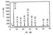
図2は、TFTデバイス構造内に付着された有機/無機混成材料のヨウ化フェネチルアンモニウムスズ(PEA)2SnI4のX線回折パターンである。(001)反射だけが存在することは、有機および無機薄板が半導体基板に平行(またはその構造のc軸が垂直)になった配向性に優れた結晶薄膜として、その材料が付着することを実証している。
【0019】
上述の有機/無機ペロブスカイトならびにその他の有機/無機混成材料は、無機の結晶半導体の利点と有機材料の利点を兼ね備える。無機成分要素は、拡張された無機の一次元、二次元または三次元ネットワークを形成して、無機の結晶性固体の高いキャリア移動度特性を潜在的に提供する。有機成分要素はこれらの材料の自己アセンブリを促進する。これにより、スピン・コーティング、浸漬コーティング、熱蒸着などの簡単な低温処理条件で材料が付着できるようになる。有機成分要素はまた無機成分要素の次元および無機ユニット間の電子結合を定義することにより無機フレームワークの電子特性を調整するのに使用される。
【0020】
図3は、典型的なTFTデバイス構造30の断面図を示す。TFT30は有機/無機混成材料層32を含む。層32は有機/無機ペロブスカイトであり、ソース電極34とドレーン電極36の間で半導体チャネルとして働く。X線回折で見られる材料の配向性は、二次元無機薄板12がソース電極34とドレーン電極36の間の電気的接続を提供するようなものである。有機/無機半導体のコンダクタンスは、SiO2薄膜などの電気絶縁層38を横切って、(縮退ドープされたn++シリコン層などの)ゲート電極40によって変調される。これらはすべて基板42によって支持される。
【0021】
ソース電極34とドレーン電極36の金属付着の前または後に、有機/無機混成材料32を付着することができる。金属付着後に有機/無機混成材料32を付着すると、その材料がメタライゼーション中に、損傷を被る可能性がある高温への露出が低減される。
【0022】
図3は典型的なFET構造の配列を示すが、本発明の範囲内で代替構造も企図される。代替FET構造のそれぞれの要素を示し、図3と同じ参照番号を付した図4を参照する。代替基板は、フレキシブルな装置を組み立てるために使用されるポリイミドやポリカーボネートなどのプラスチックを含む。このような配列では、パターン化された金属ゲート電極を、シャドー・マスクを介してまたはフォトリソグラフィによって基板上に付着する。その後、ゲート絶縁体を、それだけには限らないが、スピン・コーティング、化学的気相付着、スパッタリングまたは真空蒸着を含む様々な方法の1つによって付着する。その後、有機/無機混成材料、およびソース電極とドレーン電極を上述のように付着する。
【0023】
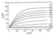
有機/無機混成材料(PEA)2SnI4で作成されたTFTの所望の電界変調されたコンダクタンスおよび電流飽和度を示す予備データを図5に示す。測定したデバイスでは、厚さ5000ÅのSiO2ゲート酸化物上に約100Åの(PEA)2SnI4層をアセトニトリルからスピン・コーティングした。半導体チャネルを、長さ70μm、幅1500μmのAu電極によって画定した。一般に、Au、Pd、Ptなど仕事関数の高い金属が、この有機/無機混成材料に対する「良好な」オーム接点を形成する。(PEA)2SnI4は、半導体層中で正孔を移動させるので、「p−タイプ」材料である。半導体チャネル(ID)中を流れる電流が負のゲート・バイアス(VG)およびソース−ドレーン電圧(VDS)と共に増加するので、このことは明白である。図6は、能動的半導体材料として有機/無機混成材料(PEA)2SnI4を備え、これまでに得られた最良の特性を示すTFTのIDSとVDSの関係をプロットしたグラフである。
【0024】
図7は、能動的半導体材料としてアルキルジアンモニウム・カチオンを含有する有機/無機混成材料(すなわち、BDASnI4(ヨウ化ブチルジアンモニウムスズ))を有するTFTのIDSとVDSの関係をプロットしたグラフである。
【0025】
0.06〜0.25cm2/V secの移動度は予想される真性値より低いが、既にアモルファス・シリコンおよび最良の有機半導体の移動度に匹敵する。具体的には、これらの移動度はスピン・コーティングされた有機半導体より高い。このようなより高い真性移動度が達成可能であると予想される。電界効果移動度は測定されていないが、ホール効果移動度に関する報告では、その範囲が約1〜100cm2/V secである。ホール移動度と電界効果移動度の関係は複雑であるが、極めて簡単な理論では、それらは比例すると予想される。したがって、これらの高いホール効果移動度は、アモルファス・シリコンの移動度を超える同様に高い電界効果移動度が達成できることを示唆している。有機/無機混成材料は、高移動度が期待できるのに加えて、無機固体に関する通常の処理技術より安価な処理技術によって付着することができる。その技術には、スピン・コーティング、浸漬コーティングおよび熱蒸着が含まれる。
【0026】
ペロブスカイト構造を有する有機/無機混成材料層を形成する1つの方法として、上記米国特許第5871579号に示された方法を使用することができる。例えば、ヨウ化ブチルジアンモニウムスズおよびヨウ化フェネチルアンモニウムスズは、SnI2フィルムを有機ヨウ化アンモニウム溶液に浸漬することによって、以下のように形成できる。
【0027】
真空室を使用して、SnI2膜の真空蒸着を行った。SnI2粉末を石英るつぼ内に装入し、上記室内に置き、系を約4×10⁻⁷Torrのベース圧力に減圧した後に蒸着を開始した。ヨウ化金属が蒸発し、室温に保持された基板上に付着し、付着中に約1×10⁻⁶Torrの圧力を達成した。典型的には、この付着中に付着速度を60〜70Å/minの範囲に保持した。
【0028】
浸漬によって上記膜を調製するために、選択した時間の間、SnI2薄膜を所望の有機ヨウ化アンモニウムを含有する溶液中に浸した。これにより、PbI2をペロブスカイト化合物に転化させる反応が生じる。
【0029】
ヨウ化ブチルジアンモニウムスズ:SnI2膜をまず、体積比1:16(1:16,v/v)の2−プロパノール/トルエンに溶かした70mM(ミリモル)のヨウ化ブチルアンモニウムの溶液中に2秒間浸し、その後トルエンですすぎ洗い、不透明な赤褐色の膜を得た。これは、366nmの携帯用ライトから励起させると僅かに橙色の光を発した。
【0030】
ヨウ化フェネチルアンモニウムスズ:SnI2膜をまず、2−プロパノール/トルエン(体積比1:16)に溶かした中のヨウ化フェネチルアンモニウムの飽和溶液中に3秒間浸漬し、その後それを溶液から取り出して、窒素雰囲気中で乾燥させることにより、ヨウ化フェネチルアンモニウムスズの膜を調製した。この手順を2回繰り返し、その結果得られた膜をヨウ化フェネチルアンモニウムの不在下で同じ混合溶媒ですすぎ洗った。その結果得られた膜は、赤褐色であり透明でなかった。
【0031】
化学的性質によって有機/無機混成材料の電子特性を調整することができる。有機/無機混成材料として使用可能な広範囲の有機および無機成分がある。この応用例の唯一の要件は、有機成分と無機成分の一方または両方が半導体であることである。化学的性質、結晶構造、無機成分の次元、ならびに有機成分の長さと化学的官能性を選択することによって、所望の特性を有する材料を設計することができる。有機/無機混成材料の化学的性質のフレキシビリティを使用して、相補型論理回路に望ましいn型およびp型の移動材料、および常時オンのTFTまたは常時オフのTFTを作成することができる。
【0032】
まとめとして、本発明の構成に関して以下の事項を開示する。
【0033】
(1)ソース領域およびドレーン領域と、
半導体の有機/無機混成材料を含み、前記ソース領域と前記ドレーン領域の間を延びるチャネル層と、
前記チャネル層に隣接して間隔をあけて配設されたゲート領域と、
前記ゲート領域と前記ソース領域、前記ドレーン領域および前記チャネル層との間の電気絶縁層とを備える電界効果トランジスタ。
(2)前記ソース領域、前記チャネル層および前記ドレーン領域が基板の表面上に配設され、前記電気絶縁層が前記チャネル層の上に配設されて前記ソース領域から前記ドレーン領域に延び、前記ゲート領域が前記電気絶縁層の上に配設される、上記(1)に記載の電界効果トランジスタ。
(3)前記ゲート領域がゲート層として基板の表面上に配設され、前記電気絶縁層が前記ゲート層上に配設され、前記ソース領域、前記チャネル層および前記ドレーン領域が前記電気絶縁層上に配設される、上記(1)に記載の電界効果トランジスタ。
(4)前記有機/無機混成材料が分子レベルで混合された有機成分要素と無機成分要素から構成される材料であり、(i)前記材料が各有機成分要素と各無機成分要素の比がほぼ一定であるという特徴を有し、(ii)少なくとも1つの成分要素が半導体であり、(iii)有機成分要素と無機成分要素が、自己アセンブリして予測可能な配列にすることのできる力を有する、上記(1)に記載の電界効果トランジスタ。
(5)前記半導体の有機/無機混成材料が、ペロブスカイト結晶構造を有する無機成分要素を含む、上記(1)に記載の電界効果トランジスタ。
(6)前記半導体の有機/無機混成材料が、アルキルモノアンモニウム・カチオンを含む、上記(5)に記載の電界効果トランジスタ。
(7)前記半導体の有機/無機混成材料がヨウ化フェネチルアンモニウムスズである(PEA)2SnI4である、上記(5)に記載の電界効果トランジスタ。
(8)前記半導体の有機/無機混成材料が、アルキルジアンモニウム・カチオンを含む、上記(5)に記載の電界効果トランジスタ。
(9)前記半導体の有機/無機混成材料が、半導体材料としてBDASnI4(ヨウ化ブチルジアンモニウムスズ)である、上記(8)に記載の電界効果トランジスタ。
(10)前記電界効果トランジスタがフレキシブル材料の基板上に形成されている、上記(1)に記載の電界効果トランジスタ。
(11)前記電界効果トランジスタがプラスチック材料の基板上に形成されている、上記(1)に記載の電界効果トランジスタ。
【図面の簡単な説明】
【図1】この場合はペロブスカイト構造に基づく、有機/無機混成材料の一例の構造を示す図である。
【図2】TFTデバイス構造内にスピン・コーティングによって付着されたヨウ化フェネチルアンモニウムスズ(PEA)2SnI4膜のX線回折パターンを示す図である。
【図3】半導体チャネルとして有機/無機混成材料を組み込んだ第1のTFT構造の断面図である。
【図4】半導体チャネルとして有機/無機混成材料を組み込んだ第2のTFT構造の断面図である。
【図5】能動的半導体材料として有機/無機混成材料(PEA)2SnI4を有するTFTのIDSとVDSの関係を示すグラフである。
【図6】能動的半導体材料として有機/無機混成材料(PEA)2SnI4を有し、これまでに得られた最良の特性を示すTFTのIDSとVDSの関係を示すグラフである。
【図7】能動的半導体材料としてアルキルジアンモニウム・カチオン(すなわち、BDASnI4(ヨウ化ブチル・ジアンモニウムスズ))を含有する有機/無機混成材料を有するTFTのIDSとVDSの関係を示すグラフである。
【符号の説明】
10 有機/無機混成材料
12 BX6八面体
20 カチオンの有機分子
30 TFTデバイス構造
32 有機/無機混成材料層
34 ソース電極
36 ドレーン電極
38 電気絶縁層
40 ゲート電極
42 基板[0001]
BACKGROUND OF THE INVENTION
The present invention relates to a thin film field effect transistor structure, and more particularly to a transistor structure using an organic / inorganic hybrid material as an internal semiconductor channel.
[0002]
[Prior art]
Thin film transistors known as TFTs are widely used as switching elements in electronic circuits, especially in large area applications such as active matrix liquid crystal displays. A TFT is an example of a field effect transistor (FET). The best-known FET is a MOSFET (Metal Oxide Semiconductor FET), which is today's normal switching element for high speed electronic applications. MOSFET refers specifically to a SiO2 / bulk Si transistor, but a more common metal-insulator-semiconductor combination is known as a MISFET. A TFT is a MISFET with an active semiconductor layer deposited as a thin film.
[0003]
Currently, TFTs in most devices are made using amorphous silicon as the semiconductor. Amorphous silicon provides the necessary conditions to reduce the cost of an inexpensive alternative to crystalline silicon, ie, a transistor used in large area applications. Amorphous silicon has a mobility of 10−1 cm2 / V sec and is 15,000 times lower than that of crystalline silicon, so its application is limited to relatively low-speed devices. Amorphous silicon deposition is less expensive than crystalline silicon, but amorphous silicon deposition requires a costly process such as plasma enhanced chemical vapor deposition.
[0004]
Recently, organic semiconductors have attracted attention as potential semiconductor components for TFTs. See, for example, Garnier et al. US Pat. No. 5,347,144 entitled “Thin-Layer Field Effect Transistors With MIS Structure Whose Insulator and Semiconductor Are Made of Organic Materials”. Organic materials (eg small molecules, short chain oligomers and polymers) are easier to process by methods such as spin coating or dip coating from solution, thermal evaporation, screen printing, etc. It becomes a cheaper alternative to inorganic materials. However, although the mobility of organic materials has improved, only the best material has a mobility that is still low and close to that of amorphous silicon.
[0005]
Organic semiconductors are cheaper than conventional amorphous silicon and are easy to adhere. Such organic materials are small molecules (eg, pentacene, metal phthalocyanine), short chain oligomers (eg, n-thiophene with n = 3-8), or long chain polymers (eg, polyalkylthiophene or polyphenylene vinylene). Overlap of atomic orbitals between adjacent multiple bonded atoms, known as conjugation, allows charge transfer along molecules, oligomers and polymers. The overlap of molecular orbitals between adjacent molecules allows charge transfer between molecules.
[0006]
A thin film of a small molecule or a short chain oligomer exhibits the highest mobility as an organic material. Small molecules or short chain oligomers exhibiting such high mobility are deposited by thermal evaporation and are deposited as highly ordered thin films. This highly ordered arrangement within the film results in orbital overlap and thus charge transfer between adjacent molecules. Long chain polymers are advantageous because they are highly soluble and can be attached by low cost techniques such as spin coating and dip coating, but have lower mobility due to their more irregular arrangement.
[0007]
Organic materials are cheaper, such as thermal evaporation, spin coating, dip coating, and open the possibility of depositing semiconductors for TFTs with easy deposition techniques, yet the mobility is still lower than desired. Typical mobility is 10−3 to 10−1 cm2 / V sec for small molecules / short chain oligomers and 10−8 to 10−2 cm2 / V sec for long chain polymers. The highest mobilities reported is 0.13 cm2 / V sec of a thin film of 0.7 cm2 / V sec, and dihexyl -α- sexithiophene of a thin film of pentacene. A mobility of 0.3 cm2 / V sec measured with single crystal α-sexithiophene is the upper limit of the mobility of this material. The mobility of organic semiconductors is comparable to that of amorphous silicon.
[0008]
Organic / inorganic hybrid materials are a well-defined class of materials that combine the useful properties of organic and inorganic component elements within a single material. Some of this class of materials exhibit semiconductor properties. In this description, the organic / inorganic hybrid material is a material composed of an organic component element and an inorganic component element mixed at a molecular level, and (i) the material has a ratio of each organic component element to each inorganic component element. (Ii) at least one component element is a semiconductor, and (iii) has the power to allow organic and inorganic component elements to self-assemble into a predictable arrangement. Is.
[0009]
An example of an organic / inorganic hybrid material takes the form of an organic / inorganic perovskite structure. The layered perovskite naturally forms a quantum well structure in which metal halide octahedral two-dimensional semiconductor layers and organic layers sharing a vertex are alternately stacked.
[0010]
Spin coating techniques are suitable for making such organic / inorganic hybrid materials. This is because many organic / inorganic perovskites are soluble in common aqueous or organic solvents. Using this method, high quality, highly oriented layered perovskite thin films are obtained. A layered perovskite film is also grown using vacuum evaporation techniques. Co-pending US patent application Ser. No. 09/192130 (filed Nov. 13, 1998) entitled “Single-Source Thermal Ablation Method for Depositing Organic-Inorganic Hybrid Films” and “Two-Step Dipping Technique for the Preparation of” US Pat. No. 5,871,579, entitled “Organic-Inorganic Perovskite Thin Films”, assigned to the same assignee as the present application, describes an alternative deposition method for organic / inorganic hybrid materials.
[0011]
[Problems to be solved by the invention]
Accordingly, it is an object of the present invention to provide an improved FET structure that uses an organic / inorganic hybrid material as a semiconductor channel.
[0012]
Another object of the present invention is to provide an improved FET structure which can be processed at low cost.
[0013]
[Means for Solving the Problems]
The FET structure according to the present invention uses a hybrid organic / inorganic material as a semiconductor channel between the source and drain electrodes of the device. This organic / inorganic material combines the advantages of an inorganic crystalline solid and an organic material. The inorganic component elements form an extended inorganic one-dimensional, two-dimensional or three-dimensional network to provide high carrier mobility characteristics of inorganic crystalline solids. Organic component elements facilitate the self-assembly of these materials, allowing them to be deposited under simple low temperature processing conditions such as spin coating, dip coating, thermal evaporation and the like. Organic component elements are also used to adjust the electronic properties of the inorganic framework by defining the dimensions of the inorganic component elements and the electronic coupling between the inorganic units.
[0014]
DETAILED DESCRIPTION OF THE INVENTION
The present invention uses a hybrid organic / inorganic material as a semiconductor channel in a thin film FET. Organic / inorganic hybrid materials, including molecular-scale composites of organic and inorganic materials, offer potentially higher carrier mobility than amorphous silicon, but are cheap and easy to attach. Inorganic component elements provide the high mobility properties of crystalline inorganic semiconductors, and organic component elements contribute to the self-assembly of materials from solution or gas phase. The organic / inorganic hybrid material can be deposited by several techniques, including spin coating, dip coating or thermal evaporation techniques. For organic semiconductors, these methods are consistent with the low cost and large area deposition requirements for large area applications. Also, the low temperature processing conditions of these deposition techniques allow these materials to be deposited on plastic substrates for flexible applications. In general, in all applications proposed for organic semiconductor materials, hybrid organic / inorganic materials can be substituted. In addition to ease of processing, the mobility of these materials is potentially higher, so amorphous silicon or organic semiconductors can be used to extend their applications to faster devices than currently possible.
[0015]
The present invention comprises a thin film FET having an organic / inorganic hybrid material as an active semiconductor layer. FIG. 1 shows an example of an organic /
[0016]
By performing a thick “cut” (n = 1 to infinity) of the n layer along the <100> or <110> plane of the perovskite, the layered inorganic compound based on the three-dimensional perovskite structure can be visualized. In the organic / inorganic hybrid material, the anionic inorganic BX6 octahedron of the perovskite sheet forms alternating layers and is charge balanced by the cationic
[0017]
The inorganic
[0018]
FIG. 2 is an X-ray diffraction pattern of the organic / inorganic hybrid material phenethylammonium tin iodide (PEA)2 SnI4 deposited in the TFT device structure. The existence of only (001) reflection demonstrates that the material adheres as a crystalline thin film with excellent orientation in which the organic and inorganic thin plates are parallel to the semiconductor substrate (or the c-axis of the structure is vertical). is doing.
[0019]
The organic / inorganic perovskites described above and other organic / inorganic hybrid materials combine the advantages of inorganic crystalline semiconductors with the advantages of organic materials. Inorganic component elements form extended inorganic one-dimensional, two-dimensional or three-dimensional networks, potentially providing the high carrier mobility properties of inorganic crystalline solids. Organic component elements facilitate the self-assembly of these materials. This allows the material to be deposited under simple low temperature processing conditions such as spin coating, dip coating, and thermal evaporation. Organic component elements are also used to tune the electronic properties of inorganic frameworks by defining the dimensions of the inorganic component elements and the electronic coupling between inorganic units.
[0020]
FIG. 3 shows a cross-sectional view of a typical
[0021]
The organic /
[0022]
Although FIG. 3 shows a typical FET structure arrangement, alternative structures are also contemplated within the scope of the present invention. Reference is made to FIG. 4 showing the respective elements of the alternative FET structure and with the same reference numbers as FIG. Alternative substrates include plastics such as polyimide and polycarbonate that are used to assemble flexible devices. In such an arrangement, a patterned metal gate electrode is deposited on the substrate through a shadow mask or by photolithography. The gate insulator is then deposited by one of a variety of methods including, but not limited to, spin coating, chemical vapor deposition, sputtering or vacuum deposition. Thereafter, the organic / inorganic hybrid material and the source and drain electrodes are deposited as described above.
[0023]
Preliminary data showing the desired field-modulated conductance and current saturation of a TFT made of organic / inorganic hybrid material (PEA)2 SnI4 is shown in FIG. In the measured device, an approximately 100 Å (PEA)2 SnI4 layer was spin coated from acetonitrile on a 5000 Å thick SiO2 gate oxide. The semiconductor channel was defined by an Au electrode 70 μm long and 1500 μm wide. In general, high work function metals such as Au, Pd, and Pt form “good” ohmic contacts to this organic / inorganic hybrid material. (PEA)2 SnI4 is a “p-type” material because it moves holes in the semiconductor layer. This is evident because the current flowing in the semiconductor channel (ID ) increases with negative gate bias (VG ) and source-drain voltage (VDS ). FIG. 6 is a graph plotting a relationship between IDS and VDS of a TFT having the organic / inorganic hybrid material (PEA)2 SnI4 as an active semiconductor material and showing the best characteristics obtained so far.
[0024]
FIG. 7 plots the relationship between IDS and VDS for a TFT having an organic / inorganic hybrid material (ie, BDASnI4 (butyldiammonium tin iodide)) containing an alkyldiammonium cation as the active semiconductor material. It is a graph.
[0025]
The mobility of 0.06-0.25 cm2 / V sec is lower than the expected intrinsic value, but is already comparable to the mobility of amorphous silicon and the best organic semiconductors. Specifically, these mobilities are higher than spin-coated organic semiconductors. It is expected that such higher intrinsic mobility can be achieved. Although field effect mobility has not been measured, a report on Hall effect mobility has a range of about 1 to 100 cm2 / V sec. The relationship between Hall mobility and field effect mobility is complex, but in a very simple theory they are expected to be proportional. Accordingly, these high Hall effect mobilities suggest that similarly high field effect mobilities can be achieved that exceed those of amorphous silicon. In addition to high mobility expected, organic / inorganic hybrid materials can be deposited by processing techniques that are cheaper than conventional processing techniques for inorganic solids. The techniques include spin coating, dip coating and thermal evaporation.
[0026]
As one method for forming an organic / inorganic hybrid material layer having a perovskite structure, the method shown in the above-mentioned US Pat. No. 5,871,579 can be used. For example, butyl diammonium tin iodide and phenethylammonium iodide can be formed by immersing a SnI2 film in an organic ammonium iodide solution as follows.
[0027]
Using a vacuum chamber, the SnI2 film was vacuum deposited. The SnI2 powder was placed in a quartz crucible, placed in the chamber, and the deposition was started after the system was depressurized to a base pressure of about 4 × 10⁻⁷ Torr. The metal iodide evaporated and deposited on the substrate held at room temperature, achieving a pressure of about 1 × 10⁻⁶ Torr during deposition. Typically, during this deposition, the deposition rate was kept in the range of 60 to 70 liters / min.
[0028]
To prepare the film by dipping, the SnI2 thin film was dipped in a solution containing the desired organic ammonium iodide for a selected time. This causes a reaction to convert PbI2 to a perovskite compound.
[0029]
A butyldiammonium iodide: SnI2 membrane was first prepared in a solution of 70 mM (mmol) butylammonium iodide dissolved in 2-propanol / toluene in a volume ratio of 1:16 (1:16, v / v). Soaking for 2 seconds and then rinsing with toluene gave an opaque reddish brown film. It emitted slightly orange light when excited from a portable light at 366 nm.
[0030]
The phenethylammonium iodide: SnI2 film was first immersed in a saturated solution of phenethylammonium iodide in 2-propanol / toluene (volume ratio 1:16) for 3 seconds, after which it was removed from the solution. A film of phenethylammonium iodide iodide was prepared by drying in a nitrogen atmosphere. This procedure was repeated twice and the resulting film was rinsed with the same mixed solvent in the absence of phenethylammonium iodide. The resulting film was reddish brown and not transparent.
[0031]
The electronic properties of the organic / inorganic hybrid material can be adjusted according to chemical properties. There are a wide range of organic and inorganic components that can be used as organic / inorganic hybrid materials. The only requirement for this application is that one or both of the organic and inorganic components are semiconductors. By selecting the chemical properties, crystal structure, dimensions of the inorganic component, and the length and chemical functionality of the organic component, a material with the desired properties can be designed. The flexibility of the organic / inorganic hybrid material chemistry can be used to create n-type and p-type transfer materials desirable for complementary logic circuits and always-on or always-off TFTs.
[0032]
In summary, the following matters are disclosed regarding the configuration of the present invention.
[0033]
(1) a source region and a drain region;
A channel layer comprising a semiconductor organic / inorganic hybrid material extending between the source region and the drain region;
A gate region spaced apart adjacent to the channel layer;
A field effect transistor comprising the gate region, the source region, the drain region, and an electrical insulating layer between the channel layer.
(2) The source region, the channel layer, and the drain region are disposed on a surface of a substrate, the electrical insulating layer is disposed on the channel layer, and extends from the source region to the drain region, The field effect transistor according to (1), wherein a gate region is disposed on the electrical insulating layer.
(3) The gate region is disposed as a gate layer on the surface of the substrate, the electrical insulating layer is disposed on the gate layer, and the source region, the channel layer, and the drain region are disposed on the electrical insulating layer. The field effect transistor according to (1) above, which is disposed in
(4) The organic / inorganic hybrid material is a material composed of an organic component element and an inorganic component element mixed at a molecular level, and (i) the ratio of each organic component element to each inorganic component element is approximately Characterized in that it is constant, (ii) at least one component element is a semiconductor, and (iii) the organic and inorganic component elements have a force that can be self-assembled into a predictable arrangement. The field effect transistor according to (1) above.
(5) The field effect transistor according to (1), wherein the semiconductor organic / inorganic hybrid material includes an inorganic component element having a perovskite crystal structure.
(6) The field effect transistor according to (5), wherein the organic / inorganic hybrid material of the semiconductor contains an alkylmonoammonium cation.
(7) The field effect transistor according to (5), wherein the organic / inorganic hybrid material of the semiconductor is (PEA)2 SnI4 which is phenethylammonium tin iodide.
(8) The field effect transistor according to (5), wherein the organic / inorganic hybrid material of the semiconductor contains an alkyldiammonium cation.
(9) The field effect transistor according to (8), wherein the semiconductor organic / inorganic hybrid material is BDASnI4 (butyldiammonium iodide) as a semiconductor material.
(10) The field effect transistor according to (1), wherein the field effect transistor is formed on a substrate of a flexible material.
(11) The field effect transistor according to (1), wherein the field effect transistor is formed on a plastic material substrate.
[Brief description of the drawings]
FIG. 1 is a diagram showing an example of the structure of an organic / inorganic hybrid material based on a perovskite structure in this case.
FIG. 2 is an X-ray diffraction pattern of phenethylammonium tin iodide (PEA)2 SnI4 film deposited by spin coating in a TFT device structure.
FIG. 3 is a cross-sectional view of a first TFT structure incorporating an organic / inorganic hybrid material as a semiconductor channel.
FIG. 4 is a cross-sectional view of a second TFT structure incorporating an organic / inorganic hybrid material as a semiconductor channel.
FIG. 5 is a graph showing the relationship between IDS and VDS of a TFT having an organic / inorganic hybrid material (PEA)2 SnI4 as an active semiconductor material.
FIG. 6 is a graph showing the relationship between IDS and VDS of a TFT having organic / inorganic hybrid material (PEA)2 SnI4 as an active semiconductor material and showing the best characteristics obtained so far.
FIG. 7 shows the relationship between IDS and VDS of a TFT having an organic / inorganic hybrid material containing an alkyldiammonium cation (ie, BDASnI4 (Butyl butyl diammonium tin)) as an active semiconductor material. It is a graph.
[Explanation of symbols]
10 organic /
Claims (10)
Translated fromJapanese前記ソース領域と前記ドレーン領域の間を延びて設けられ、0.06〜0.25cm2/Vsecのキャリア移動度特性を有する半導体として働く八面体構造の無機成分要素の層相互間に、該八面体構造の無機成分要素の層の電荷平衡をとるための有機成分要素が存在している、ヨウ化フェネチルアンモニウムスズ((PEA)2SnI4)の有機/無機混成材料のチャネル層と、
前記チャネル層に隣接して間隔をあけて配設されたゲート領域と、
前記ゲート領域と前記ソース領域、前記ドレーン領域および前記チャネル層との間の電気絶縁層とを備える、スイッチング素子として働く電界効果トランジスタ。A source region and a drain region;
Between the layers of the octahedral structure inorganic component elements provided between the source region and the drain region and serving as a semiconductor havinga carrier mobility characteristicof0.06 to0.25 cm2/ Vsec. A channel layerof an organic / inorganic hybrid material ofphenethylammonium tin iodide ((PEA)2SnI4) in which an organic component element is present for charge balancing of the layer of the inorganic component element of thefaceted structure;
A gate region spaced apart adjacent to the channel layer;
A field effect transistor serving as a switching element, comprising: the gate region, the source region, the drain region, and an electrically insulating layer between the channel layer.
ヨウ化フェネチルアンモニウムスズ((PEA)2SnI4)である有機/無機混成材料をスピン・コーティング、浸漬コーティング、又は熱蒸着により前記チャネル領域に付着することを特徴とする、電界効果トランジスタの製造方法。A source region and a drain region; a channel layer provided extending between the source region and the drain region; a gate region disposed adjacent to the channel layer and spaced apart; and the gate region and the source region In the method of manufacturing a field effect transistor serving as a switching element, comprising the drain region and an electrical insulating layer between the channel layer,
A method of manufacturing a field effect transistor, characterized in that an organic / inorganic hybrid material which is phenethylammonium tin iodide ((PEA)2 SnI4 ) is attached to the channel region by spin coating, dip coating, or thermal evaporation. .
Applications Claiming Priority (2)
| Application Number | Priority Date | Filing Date | Title |
|---|---|---|---|
| US09/261515 | 1999-03-03 | ||
| US09/261,515US6180956B1 (en) | 1999-03-03 | 1999-03-03 | Thin film transistors with organic-inorganic hybrid materials as semiconducting channels |
Publications (2)
| Publication Number | Publication Date |
|---|---|
| JP2000260999A JP2000260999A (en) | 2000-09-22 |
| JP3872246B2true JP3872246B2 (en) | 2007-01-24 |
Family
ID=22993656
Family Applications (1)
| Application Number | Title | Priority Date | Filing Date |
|---|---|---|---|
| JP2000050047AExpired - Fee RelatedJP3872246B2 (en) | 1999-03-03 | 2000-02-25 | Field effect transistor having organic / inorganic hybrid material as semiconductor channel and method of manufacturing the same |
Country Status (7)
| Country | Link |
|---|---|
| US (1) | US6180956B1 (en) |
| JP (1) | JP3872246B2 (en) |
| KR (1) | KR100351651B1 (en) |
| CN (1) | CN1145218C (en) |
| DE (1) | DE10006257B8 (en) |
| SG (1) | SG82680A1 (en) |
| TW (1) | TW461116B (en) |
Families Citing this family (86)
| Publication number | Priority date | Publication date | Assignee | Title |
|---|---|---|---|---|
| US6344662B1 (en)* | 1997-03-25 | 2002-02-05 | International Business Machines Corporation | Thin-film field-effect transistor with organic-inorganic hybrid semiconductor requiring low operating voltages |
| US6429318B1 (en)* | 2000-02-07 | 2002-08-06 | International Business Machines Corporaiton | Layered organic-inorganic perovskites having metal-deficient inorganic frameworks |
| US7875975B2 (en) | 2000-08-18 | 2011-01-25 | Polyic Gmbh & Co. Kg | Organic integrated circuit completely encapsulated by multi-layered barrier and included in RFID tag |
| DE10043204A1 (en) | 2000-09-01 | 2002-04-04 | Siemens Ag | Organic field-effect transistor, method for structuring an OFET and integrated circuit |
| KR100477394B1 (en)* | 2000-11-01 | 2005-03-17 | 인터내셔널 비지네스 머신즈 코포레이션 | Thin-film field-effect transistor with organic-inorganic hybrid semiconductor requiring low operating voltages |
| US6838198B2 (en)* | 2000-12-07 | 2005-01-04 | Industrial Research Limited | Organic/inorganic-oxide multilayer materials |
| DE10061297C2 (en) | 2000-12-08 | 2003-05-28 | Siemens Ag | Procedure for structuring an OFET |
| DE10105914C1 (en)* | 2001-02-09 | 2002-10-10 | Siemens Ag | Organic field effect transistor with photo-structured gate dielectric and a method for its production |
| CN100367528C (en)* | 2001-05-07 | 2008-02-06 | 先进微装置公司 | Switching device with memory effect |
| US6437422B1 (en)* | 2001-05-09 | 2002-08-20 | International Business Machines Corporation | Active devices using threads |
| JP3714918B2 (en)* | 2001-07-31 | 2005-11-09 | 独立行政法人科学技術振興機構 | Radiation detector |
| DE10151036A1 (en) | 2001-10-16 | 2003-05-08 | Siemens Ag | Isolator for an organic electronic component |
| DE10151440C1 (en) | 2001-10-18 | 2003-02-06 | Siemens Ag | Organic electronic component for implementing an encapsulated partially organic electronic component has components like a flexible foil as an antenna, a diode or capacitor and an organic transistor. |
| DE10160732A1 (en) | 2001-12-11 | 2003-06-26 | Siemens Ag | OFET used e.g. in RFID tag, comprises an intermediate layer on an active semiconductor layer |
| US7105360B2 (en)* | 2002-03-08 | 2006-09-12 | International Business Machines Corporation | Low temperature melt-processing of organic-inorganic hybrid |
| DE10212640B4 (en) | 2002-03-21 | 2004-02-05 | Siemens Ag | Logical components made of organic field effect transistors |
| DE10226370B4 (en) | 2002-06-13 | 2008-12-11 | Polyic Gmbh & Co. Kg | Substrate for an electronic component, use of the substrate, methods for increasing the charge carrier mobility and organic field effect transistor (OFET) |
| JP4635410B2 (en)* | 2002-07-02 | 2011-02-23 | ソニー株式会社 | Semiconductor device and manufacturing method thereof |
| US8044517B2 (en) | 2002-07-29 | 2011-10-25 | Polyic Gmbh & Co. Kg | Electronic component comprising predominantly organic functional materials and a method for the production thereof |
| DE10253154A1 (en) | 2002-11-14 | 2004-05-27 | Siemens Ag | Biosensor, used to identify analyte in liquid sample, has test field with detector, where detector registers field changes as electrical signals for evaluation |
| EP1563553B1 (en) | 2002-11-19 | 2007-02-14 | PolyIC GmbH & Co. KG | Organic electronic circuitcomprising a structured, semi-conductive functional layer and a method for producing said component |
| EP1586004B1 (en)* | 2003-01-09 | 2011-01-26 | PolyIC GmbH & Co. KG | Board or substrate for an organic electronic device and use thereof |
| DE10302149A1 (en) | 2003-01-21 | 2005-08-25 | Siemens Ag | Use of conductive carbon black / graphite blends for the production of low-cost electronics |
| US20040183070A1 (en)* | 2003-03-21 | 2004-09-23 | International Business Machines Corporation | Solution processed pentacene-acceptor heterojunctions in diodes, photodiodes, and photovoltaic cells and method of making same |
| JP4586334B2 (en)* | 2003-05-07 | 2010-11-24 | ソニー株式会社 | Field effect transistor and manufacturing method thereof |
| JP4547864B2 (en)* | 2003-05-20 | 2010-09-22 | ソニー株式会社 | Field effect transistor and manufacturing method thereof |
| JP4470398B2 (en)* | 2003-06-23 | 2010-06-02 | Tdk株式会社 | Field effect transistor |
| CN100490205C (en)* | 2003-07-10 | 2009-05-20 | 国际商业机器公司 | Method for depositing metal sulfur family film and method for preparing field effect transistor |
| US6875661B2 (en)* | 2003-07-10 | 2005-04-05 | International Business Machines Corporation | Solution deposition of chalcogenide films |
| CN100456499C (en)* | 2003-07-17 | 2009-01-28 | 松下电器产业株式会社 | Thin film transistor and manufacturing method thereof |
| DE10338277A1 (en)* | 2003-08-20 | 2005-03-17 | Siemens Ag | Organic capacitor with voltage controlled capacity |
| DE10339036A1 (en) | 2003-08-25 | 2005-03-31 | Siemens Ag | Organic electronic component with high-resolution structuring and manufacturing method |
| DE10340644B4 (en)* | 2003-09-03 | 2010-10-07 | Polyic Gmbh & Co. Kg | Mechanical controls for organic polymer electronics |
| DE10340643B4 (en)* | 2003-09-03 | 2009-04-16 | Polyic Gmbh & Co. Kg | Printing method for producing a double layer for polymer electronics circuits, and thereby produced electronic component with double layer |
| US7242041B2 (en)* | 2003-09-22 | 2007-07-10 | Lucent Technologies Inc. | Field-effect transistors with weakly coupled layered inorganic semiconductors |
| DE102004002024A1 (en)* | 2004-01-14 | 2005-08-11 | Siemens Ag | Self-aligning gate organic transistor and method of making the same |
| CN1929927B (en)* | 2004-03-10 | 2011-06-15 | 旭化成株式会社 | Condensed polycyclic aromatic compound thin film and method for producing condensed polycyclic aromatic compound thin film |
| US8241946B2 (en)* | 2004-04-27 | 2012-08-14 | Creator Technology B.V. | Method of forming an organic semiconducting device by a melt technique |
| GB2416428A (en)* | 2004-07-19 | 2006-01-25 | Seiko Epson Corp | Method for fabricating a semiconductor element from a dispersion of semiconductor particles |
| DE102004040831A1 (en)* | 2004-08-23 | 2006-03-09 | Polyic Gmbh & Co. Kg | Radio-tag compatible outer packaging |
| JP4767856B2 (en)* | 2004-08-31 | 2011-09-07 | パナソニック株式会社 | Method for manufacturing field effect transistor |
| JP4622424B2 (en)* | 2004-09-29 | 2011-02-02 | ソニー株式会社 | Method for manufacturing insulated gate field effect transistor |
| US7811438B2 (en)* | 2004-12-08 | 2010-10-12 | Palo Alto Research Center Incorporated | Bio-enrichment device to enhance sample collection and detection |
| DE102004059465A1 (en)* | 2004-12-10 | 2006-06-14 | Polyic Gmbh & Co. Kg | recognition system |
| DE102004059464A1 (en)* | 2004-12-10 | 2006-06-29 | Polyic Gmbh & Co. Kg | Electronic component with modulator |
| DE102004059467A1 (en)* | 2004-12-10 | 2006-07-20 | Polyic Gmbh & Co. Kg | Gate made of organic field effect transistors |
| DE102004063435A1 (en) | 2004-12-23 | 2006-07-27 | Polyic Gmbh & Co. Kg | Organic rectifier |
| DE102005009819A1 (en) | 2005-03-01 | 2006-09-07 | Polyic Gmbh & Co. Kg | electronics assembly |
| DE102005009820A1 (en)* | 2005-03-01 | 2006-09-07 | Polyic Gmbh & Co. Kg | Electronic assembly with organic logic switching elements |
| DE102005017655B4 (en)* | 2005-04-15 | 2008-12-11 | Polyic Gmbh & Co. Kg | Multilayer composite body with electronic function |
| WO2007005618A2 (en)* | 2005-06-30 | 2007-01-11 | The Regents Of The University Of California | High performance organic thin film transistor |
| DE102005031448A1 (en) | 2005-07-04 | 2007-01-11 | Polyic Gmbh & Co. Kg | Activatable optical layer |
| DE102005035589A1 (en) | 2005-07-29 | 2007-02-01 | Polyic Gmbh & Co. Kg | Manufacturing electronic component on surface of substrate where component has two overlapping function layers |
| DE102005035590A1 (en)* | 2005-07-29 | 2007-02-01 | Polyic Gmbh & Co. Kg | Electronic component has flexible substrate and stack of layers including function layer on substratesurface |
| DE102005042166A1 (en)* | 2005-09-06 | 2007-03-15 | Polyic Gmbh & Co.Kg | Organic device and such a comprehensive electrical circuit |
| US7681738B2 (en)* | 2005-09-12 | 2010-03-23 | Palo Alto Research Center Incorporated | Traveling wave arrays, separation methods, and purification cells |
| DE102005044306A1 (en)* | 2005-09-16 | 2007-03-22 | Polyic Gmbh & Co. Kg | Electronic circuit and method for producing such |
| KR100684926B1 (en)* | 2005-09-26 | 2007-02-20 | 연세대학교 산학협력단 | Manufacturing method of organic-inorganic hybrid field effect transistor |
| JP2007150097A (en)* | 2005-11-29 | 2007-06-14 | Toshiba Corp | Semiconductor device and manufacturing method thereof |
| DE102005059608B4 (en)* | 2005-12-12 | 2009-04-02 | Polyic Gmbh & Co. Kg | Organic electronic device with improved voltage stability and method of manufacture therefor |
| KR100674575B1 (en) | 2006-02-01 | 2007-01-29 | 한양대학교 산학협력단 | Organic-Inorganic Hybrid Field Effect Transistors and Manufacturing Method Thereof |
| KR101117006B1 (en) | 2006-12-26 | 2012-04-12 | 아사히 가세이 케미칼즈 가부시키가이샤 | Resin composition for printing plate |
| KR101288841B1 (en)* | 2006-12-29 | 2013-07-23 | 엘지디스플레이 주식회사 | Thin film transistor array substrate and method for fabricating the same |
| KR101425131B1 (en)* | 2008-01-15 | 2014-07-31 | 삼성디스플레이 주식회사 | Display substrate and display device comprising the same |
| US7879678B2 (en)* | 2008-02-28 | 2011-02-01 | Versatilis Llc | Methods of enhancing performance of field-effect transistors and field-effect transistors made thereby |
| US8686404B2 (en) | 2008-12-08 | 2014-04-01 | The Trustees Of The University Of Pennsylvania | Organic semiconductors capable of ambipolar transport |
| CN101752499B (en)* | 2008-12-12 | 2012-08-08 | 北京化工大学 | Inorganic-pentacene like substance compound semiconductor material and preparation method thereof |
| US8164089B2 (en)* | 2009-10-08 | 2012-04-24 | Xerox Corporation | Electronic device |
| WO2013171520A1 (en) | 2012-05-18 | 2013-11-21 | Isis Innovation Limited | Optoelectronic device comprising perovskites |
| GB201208793D0 (en) | 2012-05-18 | 2012-07-04 | Isis Innovation | Optoelectronic device |
| US10388897B2 (en) | 2012-05-18 | 2019-08-20 | Oxford University Innovation Limited | Optoelectronic device comprising porous scaffold material and perovskites |
| KR102698732B1 (en) | 2012-09-18 | 2024-08-27 | 옥스포드 유니버시티 이노베이션 리미티드 | Optoelectonic device |
| US10297754B2 (en) | 2014-08-01 | 2019-05-21 | International Business Machines Corporation | Techniques for perovskite layer crystallization |
| KR101655648B1 (en)* | 2015-01-30 | 2016-09-07 | 포항공과대학교 산학협력단 | Organic-inorganic hybrid perovskite light emitting transister and method of fabricating thereof |
| CN104680054A (en)* | 2015-02-11 | 2015-06-03 | 成都布林特信息技术有限公司 | RFID (radio frequency identification devices) data processing method |
| CN104766893B (en)* | 2015-04-17 | 2018-11-30 | 南开大学 | A kind of thin film transistor (TFT) and preparation method thereof |
| US9711760B2 (en) | 2015-06-30 | 2017-07-18 | Nanyang Technological University | Light-emitting device, method of forming and operating the same |
| US10665797B2 (en)* | 2015-11-09 | 2020-05-26 | Wake Forest University | Hybrid halide perovskite-based field effect transistors |
| WO2017086337A1 (en)* | 2015-11-17 | 2017-05-26 | 国立大学法人九州大学 | Two-dimensional perovskite forming material, laminate, element, and transistor |
| JP6714412B2 (en)* | 2015-11-17 | 2020-06-24 | 国立大学法人九州大学 | Two-dimensional perovskite forming material, laminate, device and transistor |
| US9793056B1 (en) | 2016-08-10 | 2017-10-17 | The United States Of America As Represented By The Secretary Of The Air Force | Method for producing high quality, ultra-thin organic-inorganic hybrid perovskite |
| US10431393B2 (en) | 2017-03-08 | 2019-10-01 | United States Of America As Represented By The Secretary Of The Air Force | Defect mitigation of thin-film hybrid perovskite and direct writing on a curved surface |
| CN108609659A (en)* | 2018-05-31 | 2018-10-02 | 青岛科技大学 | A kind of semiconductive composite material and preparation method of modification |
| CN110767807A (en)* | 2018-07-27 | 2020-02-07 | 中国科学院长春光学精密机械与物理研究所 | Has photosensitive field effect transistors formed by using perovskite thin single crystals |
| US10734582B1 (en) | 2018-08-23 | 2020-08-04 | Government Of The United States As Represented By The Secretary Of The Air Force | High-speed hybrid perovskite processing |
| EP4080584A4 (en)* | 2019-12-20 | 2023-12-20 | Mitsubishi Materials Corporation | TRANSISTOR SENSOR AND METHOD FOR DETECTING BIOMATERIALS |
Family Cites Families (9)
| Publication number | Priority date | Publication date | Assignee | Title |
|---|---|---|---|---|
| JP3135899B2 (en)* | 1989-06-06 | 2001-02-19 | 株式会社リコー | Electrical element |
| DE4010328C2 (en)* | 1989-03-31 | 1998-01-29 | Fuji Xerox Co Ltd | Electrophotographic recording material and process for its production |
| US5206525A (en)* | 1989-12-27 | 1993-04-27 | Nippon Petrochemicals Co., Ltd. | Electric element capable of controlling the electric conductivity of π-conjugated macromolecular materials |
| FR2664430B1 (en) | 1990-07-04 | 1992-09-18 | Centre Nat Rech Scient | THIN FILM FIELD EFFECT TRANSISTOR WITH MIS STRUCTURE, IN WHICH THE INSULATION AND THE SEMICONDUCTOR ARE MADE OF ORGANIC MATERIALS. |
| JPH06151872A (en)* | 1992-11-09 | 1994-05-31 | Mitsubishi Kasei Corp | Fet device |
| EP0864182B1 (en)* | 1995-11-28 | 2003-08-13 | International Business Machines Corporation | Organic/inorganic alloys used to improve organic electroluminescent devices |
| US5882548A (en)* | 1997-05-08 | 1999-03-16 | International Business Machines Corporation | Luminescent organic-inorganic perovskites with a divalent rare earth metal halide framework |
| US5871579A (en)* | 1997-09-25 | 1999-02-16 | International Business Machines Corporation | Two-step dipping technique for the preparation of organic-inorganic perovskite thin films |
| US6117498A (en)* | 1998-11-13 | 2000-09-12 | International Business Machines Corporation | Single source thermal ablation method for depositing organic-inorganic hybrid films |
- 1999
- 1999-03-03USUS09/261,515patent/US6180956B1/ennot_activeExpired - Lifetime
- 2000
- 2000-02-02CNCNB001018841Apatent/CN1145218C/ennot_activeExpired - Lifetime
- 2000-02-11SGSG200000788Apatent/SG82680A1/enunknown
- 2000-02-11DEDE10006257Apatent/DE10006257B8/ennot_activeExpired - Fee Related
- 2000-02-15TWTW089102503Apatent/TW461116B/ennot_activeIP Right Cessation
- 2000-02-18KRKR1020000007747Apatent/KR100351651B1/ennot_activeExpired - Fee Related
- 2000-02-25JPJP2000050047Apatent/JP3872246B2/ennot_activeExpired - Fee Related
Also Published As
| Publication number | Publication date |
|---|---|
| CN1145218C (en) | 2004-04-07 |
| KR20000062567A (en) | 2000-10-25 |
| DE10006257A1 (en) | 2000-09-14 |
| KR100351651B1 (en) | 2002-09-11 |
| CN1266287A (en) | 2000-09-13 |
| JP2000260999A (en) | 2000-09-22 |
| DE10006257B8 (en) | 2006-12-14 |
| TW461116B (en) | 2001-10-21 |
| SG82680A1 (en) | 2001-08-21 |
| DE10006257B4 (en) | 2006-06-29 |
| US6180956B1 (en) | 2001-01-30 |
Similar Documents
| Publication | Publication Date | Title |
|---|---|---|
| JP3872246B2 (en) | Field effect transistor having organic / inorganic hybrid material as semiconductor channel and method of manufacturing the same | |
| Yang et al. | Effects of thin film processing on pentacene/C60 bilayer solar cell performance | |
| US8614437B2 (en) | Organic underlayers that improve the performance of organic semiconductors | |
| Mitzi | Solution-processed inorganic semiconductors | |
| US6620657B2 (en) | Method of forming a planar polymer transistor using substrate bonding techniques | |
| Sirringhaus et al. | Bis (dithienothiophene) organic field-effect transistors with a high ON/OFF ratio | |
| US5892244A (en) | Field effect transistor including πconjugate polymer and liquid crystal display including the field effect transistor | |
| JP4736324B2 (en) | Semiconductor device and manufacturing method thereof | |
| US20030054586A1 (en) | Method of manufacturing high-mobility organic thin films using organic vapor phase deposition | |
| US20020164835A1 (en) | Organic n-channel semiconductor device of N,N' 3,4,9,10 perylene tetracarboxylic diimide | |
| Gao et al. | (TFPP) Eu [Pc (OPh) 8] Eu [Pc (OPh) 8]/CuPc two-component bilayer heterojunction-based organic transistors with high ambipolar performance | |
| KR20080040119A (en) | Method for manufacturing organic thin film transistor using self-assembled monolayer film-forming compound containing dichlorophosphoryl group | |
| JP2004115805A (en) | Organic gate insulating film and organic thin film transistor using the same | |
| JP2010500745A (en) | Use of perylene diimide derivatives as air-stable N-channel organic semiconductors | |
| CA2549107A1 (en) | Organic thin film transistors with multilayer electrodes | |
| JPWO2007125671A1 (en) | Field effect transistor | |
| US7151275B2 (en) | Reducing the contact resistance in organic field-effect transistors with palladium contacts by using nitriles and isonitriles | |
| CN103907215A (en) | Organic thin film transistors and method of making them | |
| JP4224578B2 (en) | Organic thin film transistor | |
| JP4429584B2 (en) | Vertical field effect transistor | |
| JPH0469971A (en) | field effect transistor | |
| JP2005232136A (en) | Polyacene compound precursor and method for synthesizing polyacene compound | |
| US7309876B2 (en) | Organic semiconductor having polymeric and nonpolymeric constituents | |
| EP2157119B1 (en) | Electronic device comprising semiconducting polymers | |
| JP2008527754A (en) | Organic thin film transistor |
Legal Events
| Date | Code | Title | Description |
|---|---|---|---|
| A131 | Notification of reasons for refusal | Free format text:JAPANESE INTERMEDIATE CODE: A131 Effective date:20040921 | |
| A601 | Written request for extension of time | Free format text:JAPANESE INTERMEDIATE CODE: A601 Effective date:20041215 | |
| A602 | Written permission of extension of time | Free format text:JAPANESE INTERMEDIATE CODE: A602 Effective date:20050111 | |
| A521 | Request for written amendment filed | Free format text:JAPANESE INTERMEDIATE CODE: A523 Effective date:20050309 | |
| A02 | Decision of refusal | Free format text:JAPANESE INTERMEDIATE CODE: A02 Effective date:20060516 | |
| A521 | Request for written amendment filed | Free format text:JAPANESE INTERMEDIATE CODE: A523 Effective date:20060731 | |
| A911 | Transfer to examiner for re-examination before appeal (zenchi) | Free format text:JAPANESE INTERMEDIATE CODE: A911 Effective date:20060919 | |
| TRDD | Decision of grant or rejection written | ||
| A01 | Written decision to grant a patent or to grant a registration (utility model) | Free format text:JAPANESE INTERMEDIATE CODE: A01 Effective date:20061010 | |
| A61 | First payment of annual fees (during grant procedure) | Free format text:JAPANESE INTERMEDIATE CODE: A61 Effective date:20061019 | |
| R150 | Certificate of patent or registration of utility model | Free format text:JAPANESE INTERMEDIATE CODE: R150 | |
| FPAY | Renewal fee payment (event date is renewal date of database) | Free format text:PAYMENT UNTIL: 20091027 Year of fee payment:3 | |
| FPAY | Renewal fee payment (event date is renewal date of database) | Free format text:PAYMENT UNTIL: 20101027 Year of fee payment:4 | |
| FPAY | Renewal fee payment (event date is renewal date of database) | Free format text:PAYMENT UNTIL: 20101027 Year of fee payment:4 | |
| FPAY | Renewal fee payment (event date is renewal date of database) | Free format text:PAYMENT UNTIL: 20111027 Year of fee payment:5 | |
| FPAY | Renewal fee payment (event date is renewal date of database) | Free format text:PAYMENT UNTIL: 20121027 Year of fee payment:6 | |
| FPAY | Renewal fee payment (event date is renewal date of database) | Free format text:PAYMENT UNTIL: 20121027 Year of fee payment:6 | |
| FPAY | Renewal fee payment (event date is renewal date of database) | Free format text:PAYMENT UNTIL: 20131027 Year of fee payment:7 | |
| R250 | Receipt of annual fees | Free format text:JAPANESE INTERMEDIATE CODE: R250 | |
| R250 | Receipt of annual fees | Free format text:JAPANESE INTERMEDIATE CODE: R250 | |
| R250 | Receipt of annual fees | Free format text:JAPANESE INTERMEDIATE CODE: R250 | |
| LAPS | Cancellation because of no payment of annual fees |