JP3870778B2 - Manufacturing method of element-embedded substrate and element-embedded substrate - Google Patents
Manufacturing method of element-embedded substrate and element-embedded substrateDownload PDFInfo
- Publication number
- JP3870778B2 JP3870778B2JP2001387428AJP2001387428AJP3870778B2JP 3870778 B2JP3870778 B2JP 3870778B2JP 2001387428 AJP2001387428 AJP 2001387428AJP 2001387428 AJP2001387428 AJP 2001387428AJP 3870778 B2JP3870778 B2JP 3870778B2
- Authority
- JP
- Japan
- Prior art keywords
- resin
- copper foil
- semiconductor chip
- layer
- recess
- Prior art date
- Legal status (The legal status is an assumption and is not a legal conclusion. Google has not performed a legal analysis and makes no representation as to the accuracy of the status listed.)
- Expired - Fee Related
Links
- 239000000758substrateSubstances0.000titleclaimsdescription54
- 238000004519manufacturing processMethods0.000titleclaimsdescription22
- 239000010410layerSubstances0.000claimsdescription89
- 239000004065semiconductorSubstances0.000claimsdescription74
- RYGMFSIKBFXOCR-UHFFFAOYSA-NCopperChemical compound[Cu]RYGMFSIKBFXOCR-UHFFFAOYSA-N0.000claimsdescription66
- 239000011889copper foilSubstances0.000claimsdescription61
- 229920005989resinPolymers0.000claimsdescription51
- 239000011347resinSubstances0.000claimsdescription51
- 239000004020conductorSubstances0.000claimsdescription40
- 239000000853adhesiveSubstances0.000claimsdescription31
- 230000001070adhesive effectEffects0.000claimsdescription31
- 238000000034methodMethods0.000claimsdescription28
- 239000011229interlayerSubstances0.000claimsdescription21
- 239000000463materialSubstances0.000claimsdescription15
- 230000004888barrier functionEffects0.000claimsdescription9
- 238000003672processing methodMethods0.000claimsdescription9
- PXHVJJICTQNCMI-UHFFFAOYSA-NNickelChemical compound[Ni]PXHVJJICTQNCMI-UHFFFAOYSA-N0.000claimsdescription8
- 238000007747platingMethods0.000claimsdescription8
- 238000004891communicationMethods0.000claimsdescription7
- 238000011161developmentMethods0.000claimsdescription5
- 229920001187thermosetting polymerPolymers0.000claimsdescription5
- KDLHZDBZIXYQEI-UHFFFAOYSA-NPalladiumChemical compound[Pd]KDLHZDBZIXYQEI-UHFFFAOYSA-N0.000claimsdescription4
- PCHJSUWPFVWCPO-UHFFFAOYSA-NgoldChemical compound[Au]PCHJSUWPFVWCPO-UHFFFAOYSA-N0.000claimsdescription4
- 229910052737goldInorganic materials0.000claimsdescription4
- 239000010931goldSubstances0.000claimsdescription4
- 229910052759nickelInorganic materials0.000claimsdescription4
- BASFCYQUMIYNBI-UHFFFAOYSA-NplatinumChemical compound[Pt]BASFCYQUMIYNBI-UHFFFAOYSA-N0.000claimsdescription4
- 238000003825pressingMethods0.000claimsdescription4
- 239000002131composite materialSubstances0.000claimsdescription3
- 239000000470constituentSubstances0.000claimsdescription3
- 229910052751metalInorganic materials0.000claimsdescription3
- 239000002184metalSubstances0.000claimsdescription3
- 238000000059patterningMethods0.000claimsdescription3
- 229910052763palladiumInorganic materials0.000claimsdescription2
- 229910052697platinumInorganic materials0.000claimsdescription2
- 239000002356single layerSubstances0.000claimsdescription2
- 238000010030laminatingMethods0.000claims3
- 238000000151depositionMethods0.000claims1
- 239000002023woodSubstances0.000claims1
- 238000012545processingMethods0.000description9
- 229910052802copperInorganic materials0.000description5
- 239000010949copperSubstances0.000description5
- 206010034972Photosensitivity reactionDiseases0.000description2
- 238000010521absorption reactionMethods0.000description2
- 229910052782aluminiumInorganic materials0.000description2
- XAGFODPZIPBFFR-UHFFFAOYSA-NaluminiumChemical compound[Al]XAGFODPZIPBFFR-UHFFFAOYSA-N0.000description2
- 239000003990capacitorSubstances0.000description2
- 229910010293ceramic materialInorganic materials0.000description2
- 238000005530etchingMethods0.000description2
- 239000011888foilSubstances0.000description2
- 238000012986modificationMethods0.000description2
- 230000004048modificationEffects0.000description2
- 239000011368organic materialSubstances0.000description2
- 239000002245particleSubstances0.000description2
- 230000036211photosensitivityEffects0.000description2
- 239000002344surface layerSubstances0.000description2
- JYEUMXHLPRZUAT-UHFFFAOYSA-N1,2,3-triazineChemical compoundC1=CN=NN=C1JYEUMXHLPRZUAT-UHFFFAOYSA-N0.000description1
- XQUPVDVFXZDTLT-UHFFFAOYSA-N1-[4-[[4-(2,5-dioxopyrrol-1-yl)phenyl]methyl]phenyl]pyrrole-2,5-dioneChemical compoundO=C1C=CC(=O)N1C(C=C1)=CC=C1CC1=CC=C(N2C(C=CC2=O)=O)C=C1XQUPVDVFXZDTLT-UHFFFAOYSA-N0.000description1
- 229920001342Bakelite®Polymers0.000description1
- 239000004593EpoxySubstances0.000description1
- BQCADISMDOOEFD-UHFFFAOYSA-NSilverChemical compound[Ag]BQCADISMDOOEFD-UHFFFAOYSA-N0.000description1
- PNEYBMLMFCGWSK-UHFFFAOYSA-Naluminium oxideInorganic materials[O-2].[O-2].[O-2].[Al+3].[Al+3]PNEYBMLMFCGWSK-UHFFFAOYSA-N0.000description1
- 230000015572biosynthetic processEffects0.000description1
- 238000007796conventional methodMethods0.000description1
- 238000001816coolingMethods0.000description1
- 238000000354decomposition reactionMethods0.000description1
- 230000000694effectsEffects0.000description1
- 238000007772electroless platingMethods0.000description1
- 238000009713electroplatingMethods0.000description1
- 239000003822epoxy resinSubstances0.000description1
- 238000007306functionalization reactionMethods0.000description1
- 239000011521glassSubstances0.000description1
- 238000010438heat treatmentMethods0.000description1
- 238000000206photolithographyMethods0.000description1
- 229920002120photoresistant polymerPolymers0.000description1
- 229920003192poly(bis maleimide)Polymers0.000description1
- 229920000647polyepoxidePolymers0.000description1
- 229920001721polyimidePolymers0.000description1
- 239000009719polyimide resinSubstances0.000description1
- 229910052594sapphireInorganic materials0.000description1
- 239000010980sapphireSubstances0.000description1
- 238000007650screen-printingMethods0.000description1
- 229910052709silverInorganic materials0.000description1
- 239000004332silverSubstances0.000description1
- 239000007787solidSubstances0.000description1
- 229920003002synthetic resinPolymers0.000description1
- 239000000057synthetic resinSubstances0.000description1
Images


Classifications
- H—ELECTRICITY
- H01—ELECTRIC ELEMENTS
- H01L—SEMICONDUCTOR DEVICES NOT COVERED BY CLASS H10
- H01L24/00—Arrangements for connecting or disconnecting semiconductor or solid-state bodies; Methods or apparatus related thereto
- H01L24/80—Methods for connecting semiconductor or other solid state bodies using means for bonding being attached to, or being formed on, the surface to be connected
- H01L24/82—Methods for connecting semiconductor or other solid state bodies using means for bonding being attached to, or being formed on, the surface to be connected by forming build-up interconnects at chip-level, e.g. for high density interconnects [HDI]
- H—ELECTRICITY
- H01—ELECTRIC ELEMENTS
- H01L—SEMICONDUCTOR DEVICES NOT COVERED BY CLASS H10
- H01L2224/00—Indexing scheme for arrangements for connecting or disconnecting semiconductor or solid-state bodies and methods related thereto as covered by H01L24/00
- H01L2224/01—Means for bonding being attached to, or being formed on, the surface to be connected, e.g. chip-to-package, die-attach, "first-level" interconnects; Manufacturing methods related thereto
- H01L2224/02—Bonding areas; Manufacturing methods related thereto
- H01L2224/04—Structure, shape, material or disposition of the bonding areas prior to the connecting process
- H01L2224/04105—Bonding areas formed on an encapsulation of the semiconductor or solid-state body, e.g. bonding areas on chip-scale packages
- H—ELECTRICITY
- H01—ELECTRIC ELEMENTS
- H01L—SEMICONDUCTOR DEVICES NOT COVERED BY CLASS H10
- H01L2224/00—Indexing scheme for arrangements for connecting or disconnecting semiconductor or solid-state bodies and methods related thereto as covered by H01L24/00
- H01L2224/01—Means for bonding being attached to, or being formed on, the surface to be connected, e.g. chip-to-package, die-attach, "first-level" interconnects; Manufacturing methods related thereto
- H01L2224/18—High density interconnect [HDI] connectors; Manufacturing methods related thereto
- H01L2224/23—Structure, shape, material or disposition of the high density interconnect connectors after the connecting process
- H01L2224/24—Structure, shape, material or disposition of the high density interconnect connectors after the connecting process of an individual high density interconnect connector
- H01L2224/241—Disposition
- H01L2224/24151—Connecting between a semiconductor or solid-state body and an item not being a semiconductor or solid-state body, e.g. chip-to-substrate, chip-to-passive
- H01L2224/24221—Connecting between a semiconductor or solid-state body and an item not being a semiconductor or solid-state body, e.g. chip-to-substrate, chip-to-passive the body and the item being stacked
- H01L2224/24225—Connecting between a semiconductor or solid-state body and an item not being a semiconductor or solid-state body, e.g. chip-to-substrate, chip-to-passive the body and the item being stacked the item being non-metallic, e.g. insulating substrate with or without metallisation
- H01L2224/24226—Connecting between a semiconductor or solid-state body and an item not being a semiconductor or solid-state body, e.g. chip-to-substrate, chip-to-passive the body and the item being stacked the item being non-metallic, e.g. insulating substrate with or without metallisation the HDI interconnect connecting to the same level of the item at which the semiconductor or solid-state body is mounted, e.g. the item being planar
- H—ELECTRICITY
- H01—ELECTRIC ELEMENTS
- H01L—SEMICONDUCTOR DEVICES NOT COVERED BY CLASS H10
- H01L2224/00—Indexing scheme for arrangements for connecting or disconnecting semiconductor or solid-state bodies and methods related thereto as covered by H01L24/00
- H01L2224/01—Means for bonding being attached to, or being formed on, the surface to be connected, e.g. chip-to-package, die-attach, "first-level" interconnects; Manufacturing methods related thereto
- H01L2224/26—Layer connectors, e.g. plate connectors, solder or adhesive layers; Manufacturing methods related thereto
- H01L2224/31—Structure, shape, material or disposition of the layer connectors after the connecting process
- H01L2224/32—Structure, shape, material or disposition of the layer connectors after the connecting process of an individual layer connector
- H01L2224/321—Disposition
- H01L2224/32151—Disposition the layer connector connecting between a semiconductor or solid-state body and an item not being a semiconductor or solid-state body, e.g. chip-to-substrate, chip-to-passive
- H01L2224/32221—Disposition the layer connector connecting between a semiconductor or solid-state body and an item not being a semiconductor or solid-state body, e.g. chip-to-substrate, chip-to-passive the body and the item being stacked
- H01L2224/32225—Disposition the layer connector connecting between a semiconductor or solid-state body and an item not being a semiconductor or solid-state body, e.g. chip-to-substrate, chip-to-passive the body and the item being stacked the item being non-metallic, e.g. insulating substrate with or without metallisation
- H—ELECTRICITY
- H01—ELECTRIC ELEMENTS
- H01L—SEMICONDUCTOR DEVICES NOT COVERED BY CLASS H10
- H01L2224/00—Indexing scheme for arrangements for connecting or disconnecting semiconductor or solid-state bodies and methods related thereto as covered by H01L24/00
- H01L2224/73—Means for bonding being of different types provided for in two or more of groups H01L2224/10, H01L2224/18, H01L2224/26, H01L2224/34, H01L2224/42, H01L2224/50, H01L2224/63, H01L2224/71
- H01L2224/732—Location after the connecting process
- H01L2224/73251—Location after the connecting process on different surfaces
- H01L2224/73267—Layer and HDI connectors
- H—ELECTRICITY
- H01—ELECTRIC ELEMENTS
- H01L—SEMICONDUCTOR DEVICES NOT COVERED BY CLASS H10
- H01L2224/00—Indexing scheme for arrangements for connecting or disconnecting semiconductor or solid-state bodies and methods related thereto as covered by H01L24/00
- H01L2224/80—Methods for connecting semiconductor or other solid state bodies using means for bonding being attached to, or being formed on, the surface to be connected
- H01L2224/82—Methods for connecting semiconductor or other solid state bodies using means for bonding being attached to, or being formed on, the surface to be connected by forming build-up interconnects at chip-level, e.g. for high density interconnects [HDI]
- H01L2224/82009—Pre-treatment of the connector or the bonding area
- H01L2224/8203—Reshaping, e.g. forming vias
- H01L2224/82035—Reshaping, e.g. forming vias by heating means
- H01L2224/82039—Reshaping, e.g. forming vias by heating means using a laser
- H—ELECTRICITY
- H01—ELECTRIC ELEMENTS
- H01L—SEMICONDUCTOR DEVICES NOT COVERED BY CLASS H10
- H01L2224/00—Indexing scheme for arrangements for connecting or disconnecting semiconductor or solid-state bodies and methods related thereto as covered by H01L24/00
- H01L2224/91—Methods for connecting semiconductor or solid state bodies including different methods provided for in two or more of groups H01L2224/80 - H01L2224/90
- H01L2224/92—Specific sequence of method steps
- H01L2224/921—Connecting a surface with connectors of different types
- H01L2224/9212—Sequential connecting processes
- H01L2224/92142—Sequential connecting processes the first connecting process involving a layer connector
- H01L2224/92144—Sequential connecting processes the first connecting process involving a layer connector the second connecting process involving a build-up interconnect
- H—ELECTRICITY
- H01—ELECTRIC ELEMENTS
- H01L—SEMICONDUCTOR DEVICES NOT COVERED BY CLASS H10
- H01L2224/00—Indexing scheme for arrangements for connecting or disconnecting semiconductor or solid-state bodies and methods related thereto as covered by H01L24/00
- H01L2224/91—Methods for connecting semiconductor or solid state bodies including different methods provided for in two or more of groups H01L2224/80 - H01L2224/90
- H01L2224/92—Specific sequence of method steps
- H01L2224/922—Connecting different surfaces of the semiconductor or solid-state body with connectors of different types
- H01L2224/9222—Sequential connecting processes
- H01L2224/92242—Sequential connecting processes the first connecting process involving a layer connector
- H01L2224/92244—Sequential connecting processes the first connecting process involving a layer connector the second connecting process involving a build-up interconnect
- H—ELECTRICITY
- H01—ELECTRIC ELEMENTS
- H01L—SEMICONDUCTOR DEVICES NOT COVERED BY CLASS H10
- H01L2924/00—Indexing scheme for arrangements or methods for connecting or disconnecting semiconductor or solid-state bodies as covered by H01L24/00
- H01L2924/06—Polymers
- H01L2924/078—Adhesive characteristics other than chemical
- H01L2924/07802—Adhesive characteristics other than chemical not being an ohmic electrical conductor
Landscapes
- Engineering & Computer Science (AREA)
- Computer Hardware Design (AREA)
- Microelectronics & Electronic Packaging (AREA)
- Power Engineering (AREA)
- Production Of Multi-Layered Print Wiring Board (AREA)
Description
Translated fromJapanese【0001】
【発明の属する技術分野】
本発明は、LSI等の半導体チップをプリント配線板の内部に収容した素子内蔵基板の製造方法および素子内蔵基板に関する。
【0002】
【従来の技術】
電子機器の小型化、多機能化に伴い、プリント配線板の高密度実装化や実装部品の小型化に対する要求が厳しくなっている。プリント配線板においては、従来、配線ルールの縮小により基板面内における高密度化が図られていたが、近年では、ビルドアップ工法等を採用してプリント配線板を多層化し、三次元的に配線を引き回して実装効率の向上が図られている。
【0003】
一方、このようなビルドアップ多層プリント配線板の開発に並行して、実装効率の更なる向上を目的として、抵抗やコンデンサ等の受動素子、LSI等の能動素子を内蔵した素子内蔵基板の開発が進められている。
【0004】
例えば特開平6−45763号公報には、図5に示すような構成の素子内蔵基板101が記載されている。素子内蔵基板101は、半導体チップ102を収容するためのキャビティ103が形成された内層基板104の両面に、外層基板105,106をそれぞれ積層した構造を有している。キャビティ103内の半導体チップ102は、外層基板105上の導体パターン107に対し、バンプ108を介して電気的に接続されている。なお、外層基板105,106の外面側には、半導体パッケージ部品109,110がそれぞれ実装されている。
【0005】
導体パターン107に対する半導体チップ102の電気的接続は、いわゆるフリップチップ実装によって行われている。すなわち、半導体チップ102の電極パッド部上に形成したバンプ108を外部電極として、導体パターン107に対し熱圧着等の公知の接合技術を用いて実装されている。
【0006】
【発明が解決しようとする課題】
上記のように、内蔵される半導体チップ102を導体パターン107に対してフリップチップ実装するためには、導体パターン107のチップ接続ランド部をバンプ108に対応した配列ピッチで形成する必要がある。このため、半導体チップ102の電極パッド部の配列ピッチが例えば60μmというようにファイン化されると、導体パターン107の接続ランド部を上記のパッドピッチに対応して形成することが困難となる。すなわち、電極パッド部のファインピッチ化に、導体パターン107が対応できないという問題がある。
【0007】
この問題を解消するために、例えば特開2000−228457号公報には、図6に示すように、半導体チップ112の能動面に対し、電極パッド部の配置を再配列するための再配線層113を設けて、バンプ114の配列ピッチを変換する方法が知られている。この方法によれば、電極パッド部の配列ピッチが60μmの場合、例えば120μmにまでバンプピッチを拡張することができる。
【0008】
しかしながら、再配線層113を形成することは、内蔵される半導体部品の製造コストの増大を招き、その製造工程の複雑化によるリードタイムの長大化や、歩留まりの低下といった種々の問題を包含することになる。
【0009】
本発明は上述の問題に鑑みてなされ、ファインピッチの電極パッド部を有する半導体チップをピッチ変換することなく、基板上の導体パターンに接続することができる素子内蔵基板の製造方法および素子内蔵基板を提供することを課題とする。
【0010】
【課題を解決するための手段】
以上の課題を解決するに当たり、本発明の素子内蔵基板の製造方法は、半導体チップを内部に収容した素子内蔵基板の製造方法であって、半導体チップを収容するための凹所を、樹脂付き銅箔の樹脂形成面側に積層された絶縁基材に形成する工程と、プリント配線板上の所定部位に能動面を上向きにして半導体チップを搭載し、上記能動面を凹所を介して樹脂形成面に密着させるとともに、プリント配線板を絶縁基材に積層する工程と、樹脂付き銅箔の銅箔側から、凹所内に収容された半導体チップの能動面上の電極パッド部に向けて、ダイレクトレーザ加工法により層間接続用の連絡孔を形成する工程と、連絡孔を介して銅箔と電極パッド部とを導通させる工程と、銅箔を所定形状にパターニングする工程とを有することを特徴としている。
【0011】
本発明の素子内蔵基板の製造方法では、樹脂付き銅箔とプリント配線板との間の絶縁基材に内蔵された半導体チップの電極パッド部を樹脂付き銅箔の表面銅箔と電気的に接続するために、樹脂付き銅箔の表面銅箔と樹脂層とを同時に穿孔できるダイレクトレーザ加工法を採用している。そして、形成された連絡孔を介して、表面銅箔と電極パッド部とを導通させるようにしている。これにより、ファインピッチに形成された半導体チップ能動面上の電極パッド部をピッチ変換することなく、樹脂付き銅箔の銅箔層に接続することができる。
【0012】
さらに、本発明の素子内蔵基板は、絶縁層と、絶縁層の一方の面に形成された導体層と、絶縁層の他方の面に形成され、半導体チップを収容可能な凹所と、絶縁層の他方の面に積層され、半導体チップをその能動面が凹所の底部に密着されるように搭載したプリント配線板と、導体層と能動面上の電極パッド部との間を導通させる層間接続部とを備え、絶縁層が、樹脂付き銅箔の樹脂層と、この樹脂層に積層され上記凹所が形成された絶縁基材とを含むことを特徴とする。
【0013】
本発明の素子内蔵基板においては、絶縁層を介して対向する導体層と半導体チップの電極パッド部とが直接層間接続されている。これにより、電極パッド部のパッド配列を再配列することなく半導体チップを基板上の導体層へ接続することができる。
【0014】
【発明の実施の形態】
以下、本発明の実施の形態について図面を参照して説明する。
【0015】
図1は、本発明の実施の形態による素子内蔵基板を示している。本実施の形態の素子内蔵基板1は、半導体チップ2を搭載したプリント配線板3の上に絶縁層4が設けられ、更に絶縁層4の上に所定形状の導体パターン5が設けられている。半導体チップ2の能動面14に配列された複数の電極パッド部6およびプリント配線板3の回路パターン(ランド)7はそれぞれ、導体パターン5に対して層間接続部8,9を介して導通されている。
【0016】
半導体チップ2は、電極パッド部6が形成された能動面14を上向きにして、プリント配線板3の回路形成面の所定部位に例えば接着剤(図示略)を介して搭載されている。半導体チップ2としては、例えばDRAM等の半導体メモリやこれにロジック回路が混載されたシステムLSI、あるいはMPU、各種ハードウェアシステムを駆動するドライバ回路、電源回路、高周波信号処理回路等がそれぞれ組み込まれた、公知の半導体ベアチップ部品が適用される。
【0017】
プリント配線板3は、本実施の形態では片面銅張積層板で構成され、絶縁基板15と、この上に形成された所定形状の回路パターン7とで構成されている。絶縁基板15の材質は特に限定されず、セラミック系材料あるいは有機系材料などの公知の材料が用いられる。セラミック系材料であれば、アルミナあるいはサファイア等が適用され、有機系材料であれば、ガラスエポキシ樹脂やポリイミド樹脂、ビスマレイミドトリアジン樹脂等が適用可能である。
【0018】
プリント配線板3と絶縁層4との間には、絶縁性の接着シート10が介装されている。接着シート10は本発明の「絶縁基材」に対応し、本実施の形態では、熱硬化性樹脂に感光性を持たせたシート材で構成され、その厚さは半導体チップ2の厚さと同等もしくは、半導体チップ2の厚さよりも若干小さく形成されている。接着シート10には、半導体チップ2を収容するための開口11が形成されている。
【0019】
絶縁層4および導体パターン5は、本実施の形態では、いわゆるRCC(Resin-Coated Copper) の呼称で知られる樹脂付き銅箔で構成されている。すなわち、絶縁層4および導体パターン5はそれぞれ、樹脂付き銅箔の合成樹脂層および表面銅箔に対応する。この樹脂付き銅箔の樹脂形成面側に接着シート10を介してプリント配線板3が積層されている。
【0020】
これら絶縁層4と接着シート10の開口11とによって、半導体チップ2が収容される凹所12が形成されている。半導体チップ2は、その能動面14が凹所12の底部13である絶縁層下面(樹脂形成面)に密着され、電極パッド部6が絶縁層4に没入している。
【0021】
ここで、本実施の形態では、半導体チップ2の電極パッド部6はアルミニウムで構成されるが、その上にニッケルめっきおよび金めっきの複合層からなるバリア層16が形成されている。このバリア層16は、後述するように、層間接続部8を形成する際に適用されるレーザービームから、電極パッド部6を保護するために設けられている。バリア層16は、ニッケル、金、パラジウム、白金等の金属めっきの単層またはこれらの複合層で構成することができる。なお、以下の説明では、特に断らない限り、電極パッド部6をバリア層16も含む意味で用いるものとする。
【0022】
プリント配線板3の回路形成面は、半導体チップ2の能動面14を凹所12の底部13に密着させた状態で、接着シート10に積層されている。また、半導体チップ2の側面と接着シート10の開口11との間の隙間には、プリント配線板3を積層する際に適用される加熱加圧プレスによって絶縁層4の構成樹脂が流入しており、これにより半導体チップ2が凹所12内においてモールドされている。
【0023】
半導体チップ2の各電極パッド部6およびプリント配線板3の回路パターン7の間は、層間接続部8,9および表層の導体パターン5を介して電気的に接続されている。層間接続部8,9は、後に詳述するように、例えば直径30μmの連絡孔に設けた導電材料で構成されている。
【0024】
本実施の形態の素子内蔵基板1は、以上のようにして構成されている。本実施の形態の素子内蔵基板1によれば、絶縁層4を介して対向する導体パターン5と半導体チップ2の電極パッド部6とが直接、層間接続部8,9を介して導通されているので、電極パッド部6のパッド配列を再配列することなく半導体チップ2を導体パターン5へ接続することができる。
【0025】
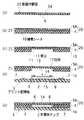
次に、以上のように構成される本実施の形態の素子内蔵基板の製造方法について、図2および図3を参照して説明する。
【0026】
まず、図2(a)に示すように、銅箔(導体層)5Aの厚さが3μm、絶縁層(樹脂層)4の厚さが20μmの樹脂付き銅箔20を準備する。本実施の形態では、樹脂付き銅箔20として、日立化成株式会社製の樹脂付き銅箔(F6000E)が用いられる。
【0027】
次に、図2(b)に示すように、絶縁層4の下面に、接着シート10を接着することによって、樹脂付き銅箔20と接着シート10との積層体25を作製する。
【0028】
接着シート10は、本実施の形態では未硬化(半硬化状態)のエポキシ系熱硬化性樹脂に感光性を付与したシート材が用いられ、その厚さは、約30μmとした。なお、接着シート10の厚さは、内蔵される半導体チップ2の厚さよりもやや小さくされるものとする。本実施の形態では、接着シート10として、住友ベークライト株式会社製の感光性接着シート(CFP2035)が用いられる。
【0029】
続いて、図2(c)に示すように、樹脂付き銅箔20に積層した接着シート10に対し、半導体チップ2を収容するための開口11を形成する。これにより、樹脂付き銅箔20の樹脂形成面側(絶縁層4側)に凹所12が形成される。開口11(凹所12)は、接着シート10の所定部位に対し、露光および現像の各処理を行うことによって形成される。開口11は、内蔵すべき半導体チップ2の外形よりもやや大きく形成される。
【0030】
ここで、接着シート10がポジ型の感光性シートであれば、露光光が照射された領域が現像液中に溶解し、ネガ型の感光性シートであれば、露光光が照射されなかった領域が現像液中に溶解することによって開口11が形成されるが、本発明では、何れのタイプの感光性シートでも用いることができる。
【0031】
なお、以上の工程では、接着シート10を絶縁層4に積層した後、接着シート10の層のみ加工して開口11(凹所12)を形成するようにしたが、これに代えて、開口11を形成した後に、接着シート10を絶縁層4に積層するようにしてもよい。
【0032】
なおまた、上記の工程では、フォトリソグラフィ技術を用いて開口11を形成できる素材として感光性のある接着シート10を用いたが、例えばプリプレグ等の未硬化の熱硬化性樹脂シートを上記接着シートとして適用し、これにプレス加工等を施して開口(凹所)を形成した後に絶縁層4へ積層するようにしてもよい。
【0033】
さて、次に、図2(d)に示すように、内蔵すべき半導体チップ2をフェイスアップ方式で(能動面14を上方に向けて)搭載したプリント配線板3と、上述した樹脂付き銅箔20および接着シート10の積層体25とを、互いに位置合わせする。
【0034】
プリント配線板3には、あらかじめ回路パターン7が形成されている。本実施の形態では、回路パターン7の厚さは約25μmとされる。プリント配線板3と半導体チップ2の裏面(非能動面)との間は、例えば接着剤等によって接着されている。また、半導体チップ2の電極パッド部6のピッチは約60μmで、アルミニウムパッドの上に、厚さ10μmの無電解ニッケルめっきと、更にその上に形成される厚さ0.1μmの無電解金めっきからなるバリア層16が形成されている。
【0035】
そして、図2(e)に示すように、プリント配線板3と積層体25とを真空中での加熱加圧プレスによって積層する。このとき、半導体チップ2の能動面14が積層体25の凹所12の底部13に密着されると同時に、プリント配線板3の回路形成面が積層体25の接着シート10に積層される。
【0036】
この加熱加圧プレスにより、半導体チップ2の電極パッド部6は絶縁層4に没入するとともに、溶融した絶縁層4の構成樹脂が、開口11(凹所12)と半導体チップ2との間の隙間に流入する。冷却後、半導体チップ2はその流入した樹脂材料によってモールドされ、凹所12内に保持される。
【0037】
図3(f)および(g)は、表層の銅箔5Aと、半導体チップ2の電極パッド部6およびプリント配線板3の回路パターン7との間の層間接続工程を示している。この工程は、銅箔5Aの所定部位に対して紫外線レーザ(以下、UVレーザという)Lを照射して、電極パッド部6および回路パターン7に到達する連絡孔18,19をそれぞれ形成する工程(図3(f))と、これらの連絡孔18,19に導電性をもたせる工程(図3(g))とを有する。
【0038】
連絡孔18,19の形成は、ダイレクトレーザ加工法によって行われる。このダイレクトレーザ加工法は、銅箔5Aおよび絶縁層4をUVレーザLの照射によって一時に穿孔するレーザ加工法の一種である。このダイレクトレーザ加工法を用いることにより、表面の銅箔と絶縁層とを別々な工程で穿孔する方法に比べて、微細な孔を形成することができる。
【0039】
すなわち、従来の樹脂付き銅箔の穿孔方法として、表面銅箔に孔径と同径のウィンド(窓)を形成した後、孔径よりも50〜100μm大きいCO2レーザで絶縁層を穿孔するコンフォーマルマスク法や、表面銅箔に孔径よりも約100μm大きなウィンドを形成した後、絶縁層をCO2レーザで穿孔するラージウィンド法が用いられていた。これは、光沢のある銅表面のレーザビームの吸収率が絶縁層よりも低いため、前もって表面の銅箔をエッチングにより除去し、開口した銅箔を介して絶縁層をレーザ加工する必要があったからである。このため、従来のレーザ加工では、ファインピッチな孔を形成することが非常に困難で、かつ、工程が複雑であった。
【0040】
一方、ダイレクトレーザ加工は、表面銅箔のレーザ吸収率を絶縁層の分解エネルギに近づけることによって、表面銅箔を絶縁層とともにレーザで同時に穿孔できるようにしたものである。本実施の形態では、このダイレクトレーザ加工に適した樹脂付き銅箔20を採用しているために、微細孔をファインピッチで容易に形成することができる。本実施の形態では、層厚が最大50μmの絶縁層(4,10)を紫外線レーザLによって、30μm程度の孔径の連絡孔18,19を形成している。
【0041】
UVレーザLは、積層体25を突き抜け、半導体チップ2の電極パッド部6に到達するが、バリア層16によってUVレーザLの進行が規制され、電極パッド部6に対する必要以上の加工が防止される。また、プリント配線板3上の回路パターン(ランド)7に到達したUVレーザLも同様に、厚い銅箔層によって必要以上の加工が制限される。以上のようにして、電極パッド部6および回路パターン(ランド)7が開口される。
【0042】
一方、連絡孔18,19に導電性をもたせる工程は、無電解めっき法と電解めっき法を併用して連絡孔18,19内に例えば銅めっきを析出させるか、あるいは、スクリーン印刷法等によって連絡孔18,19内に導電材料を充填することによって行われる。これにより、図3(g)に示すように、半導体チップ2の電極パッド部6およびプリント配線板3の回路パターン7と、表面の銅箔5Aとを電気的に接続する層間接続部8,9が形成される。
【0043】
なお、上述のように、連絡孔18,19に対して導電材料を充填することによって層間接続部8,9を形成する場合には、導電材料として、φ3μmの銀粒子を導電粒子とする導電ペーストを用いることによって、φ30μmという微細な連絡孔18,19に対して容易に導電ペーストを充填することができる。
【0044】
次に、図3(h)に示すように、銅箔5Aを所定形状にパターニングすることによって導体パターン5を形成する。本実施の形態では、プリント配線板3の回路パターン7に対して半導体チップ2を電気的に接続するようにしている。
【0045】
導体パターン5は、銅箔5A上にフォトレジストを形成し、これに露光マスクを介して所定部位を感光させ、現像処理を施してレジストパターンを形成した後、エッチングによってレジストが形成されていない領域を除去することによって形成することができる。
【0046】
以上のようにして、本実施の形態の素子内蔵基板1が製造される。本実施の形態によれば、ファインピッチに形成された電極パッド部6をピッチ変換することなく、導体パターン5に接続することができる。
【0047】
また、電極パッド部6を半導体チップ2の能動面14上でピッチ変換することなく、プリント配線板3の回路パターン7に接続することができるので、プリント配線板3上の回路パターン7を電極パッド部6の配列ピッチに対応して微細に形成せずとも、半導体チップ2と電気的に接続することができる。
【0048】
また、以上の実施の形態によれば、ダイレクトレーザ加工が適用可能な樹脂付き銅箔20を用いているので、製造工程を複雑化することなく低コストで高密度実装が可能な素子内蔵基板1を製造することができる。
【0049】
以上、本発明の実施の形態について説明したが、勿論、本発明はこれに限定されることなく、本発明の技術的思想に基づいて種々の変形が可能である。
【0050】
例えば以上の実施の形態では、層間接続用の連絡孔18,19をダイレクトレーザ加工法により形成するにあたって、UVレーザLを用いたが、勿論、これに限らない。すなわち、電極パッド部6のピッチに一定の余裕度があるならば、CO2レーザやYAGレーザ等の他のレーザ光源を用いることも可能である。
【0051】
また、以上の実施の形態では、プリント配線板3として片面銅張積層板を用いたが、図4に示すように、これを両面銅張り積層板で構成するとともに、外面側の導体層5Bをベタ箔状態とすることによって、電磁ノイズの低減に寄与することができる。また、当該ベタ箔層5Bを接地回路へ接続すれば、静電放電(ESD)対策にもなり得る。なお、図4において上述の実施の形態と対応する部分については同一の符号を付している。
【0052】
さらに、上述の実施の形態において製造した素子内蔵基板1に対して、更にその上層または下層に他のプリント配線板を積層してビルドアップ化を図ることも可能である。この場合の各導体パターン間の層間接続を、上述のダイレクトレーザ加工法で行うようにすれば、ファインピッチな層間接続部を備えた多層プリント配線板を容易に製造することができる。
【0053】
また、以上の実施の形態では、半導体チップ2を内蔵した素子内蔵基板1について説明したが、勿論、この半導体チップ2のみに限らず、他のLSIを初めとする能動素子や、抵抗またはコンデンサ等の受動素子も内蔵されていてもよい。
【0054】
【発明の効果】
以上述べたように、本発明の素子内蔵基板の製造方法によれば、ファインピッチに形成された半導体チップ能動面上の電極パッド部をピッチ変換することなく導体層に接続することができる。
【0055】
また、ダイレクトレーザ加工が適用できる樹脂付き銅箔を用いて層間接続用の連絡孔を形成する本発明の素子内蔵基板の製造方法によれば、複雑な工程を要することなく容易に層間接続部を形成することができる。
【0056】
上記銅箔と半導体チップの電極パッド部とを導通させる工程に、上記銅箔とプリント配線板の回路パターンとを導通させる工程を含めた本発明の素子内蔵基板の製造方法によれば、ファインピッチに形成された電極パッド部を半導体チップの能動面上で再配列することなく、プリント配線板上の回路パターンに接続することができる。
【0057】
さらに、本発明の素子内蔵基板によれば、絶縁層を介して対向する導体層と半導体チップの電極パッド部とが直接、層間接続部を介して導通されているので、電極パッド部のパッド配列を再配列することなく半導体チップを導体層へ接続することができる。
【図面の簡単な説明】
【図1】 本発明の実施の形態による素子内蔵基板の構成を示す断面図である。
【図2】 (a)〜(e)ともに、本発明の実施の形態による素子内蔵基板の製造方法を説明する工程断面図である。
【図3】 (f)〜(h)ともに、本発明の実施の形態による素子内蔵基板の製造工程を説明する図2に続く工程断面図である。
【図4】 本発明の実施の形態による素子内蔵基板の構成の変形例を示す断面図である。
【図5】 従来の素子内蔵基板の構成を示す断面図である。
【図6】 電極パッド部の再配線層113を能動面上に備えた従来の半導体部品の構成を示す斜視図である。
【符号の説明】
1…素子内蔵基板、2…半導体チップ、3…プリント配線板、4…絶縁層、5…導体パターン、5A…銅箔(導体層)、6…電極パッド部、7…回路パターン、8,9…層間接続部、10…接着シート(絶縁基材)、11…開口、12…凹所、13…凹所の底部、14…半導体チップの能動面、16…バリア層、18,19…連絡孔、20…樹脂付き銅箔、L…UVレーザ。[0001]
BACKGROUND OF THE INVENTION
The present invention relates to a method for manufacturing an element-embedded substrate in which a semiconductor chip such as an LSI is accommodated inside a printed wiring board, and the element-embedded substrate.
[0002]
[Prior art]
With the downsizing and multi-functionalization of electronic devices, demands for high-density mounting of printed wiring boards and miniaturization of mounted parts are becoming strict. Conventionally, in printed wiring boards, high density in the substrate surface has been achieved by reducing the wiring rules, but in recent years, multilayered printed wiring boards have been adopted using a build-up method, etc., and wiring is performed three-dimensionally. As a result, the mounting efficiency is improved.
[0003]
On the other hand, in parallel with the development of such build-up multilayer printed wiring boards, development of device-embedded boards that incorporate passive elements such as resistors and capacitors, and active elements such as LSIs, is aimed at further improving mounting efficiency. It is being advanced.
[0004]
For example, Japanese Patent Laid-Open No. 6-45763, the element built-in
[0005]
Electrical connection of the
[0006]
[Problems to be solved by the invention]
As described above, in order to flip-chip mount the built-in
[0007]
To solve this problem, for example, JP-A-2000-228457 discloses, as shown in FIG.6, the active surface of the
[0008]
However, the formation of the
[0009]
The present invention has been made in view of the above-described problems, and provides a method for manufacturing an element-embedded substrate and a device-embedded substrate that can be connected to a conductor pattern on the substrate without converting the pitch of a semiconductor chip having fine pitch electrode pad portions. The issue is to provide.
[0010]
[Means for Solving the Problems]
In solving the above problems, a method for manufacturing an element-embedded substrate according to the present invention is a method for manufacturing an element-embedded substrate in which asemiconductor chip is housed, and a recess for housing a semiconductor chip is formed with a resin-coated copper. A process of forming on an insulating base material laminated on the resin-forming surface side of the foil, and mounting a semiconductor chip with an active surface facing upward at a predetermined portion on the printed wiring board, and forming the resin on the active surface through a recess Directly from the copper foil side of the resin-coated copper foil toward the electrode pad on the active surface of the semiconductor chip housed in the recess A step of forming a connection hole for interlayer connection by a laser processing method, a step of conducting the copper foil and the electrode pad portion through the connection hole, and a step of patterning the copper foil into a predetermined shape Have
[0011]
In the manufacturing method of the element-embedded substrate of the present invention, the electrode pad portion of the semiconductor chip built inthe insulating base material betweenthe resin-coated copper foil and the printed wiring board is electrically connected to the surface copper foil of the resin-coated copper foil. In order to achieve this, a direct laser processing method capable of simultaneously perforating the surface copper foil and the resin layer of the resin-coated copper foil is employed. Then, the surface copper foil and the electrode pad portion are brought into conduction through the formed communication hole. Thereby, the electrode pad part on the active surface of the semiconductor chip formed in the fine pitch can be connected to the copper foil layer of the copper foil with resin without converting the pitch.
[0012]
Furthermore, the element-embedded substrate of the present invention includes an insulating layer, a conductor layer formed on one surface of the insulating layer, a recess formed on the other surface of the insulating layer and capable of accommodating a semiconductor chip, and an insulating layer Layered connection on the other side of the circuit board, and a conductive printed circuit board on which a semiconductor chip is mounted so that its active surface is in close contact with the bottom of the recess, and an interlayer connection for conducting between the conductor layer and the electrode pad on the active surface Andthe insulating layer includesa resin layer of a copper foil with resin and an insulating base material laminated on the resin layer and having the recess formed therein .
[0013]
In the element-embedded substrate of the present invention, the opposing conductor layer and the electrode pad portion of the semiconductor chip are directly connected to each other via an insulating layer. Thereby, the semiconductor chip can be connected to the conductor layer on the substrate without rearranging the pad arrangement of the electrode pad portion.
[0014]
DETAILED DESCRIPTION OF THE INVENTION
Hereinafter, will be described with reference to the drawingsimplementation of the present invention.
[0015]
Figure 1 shows a device embedded substrate according tothe implementation of the embodimentof the present invention. In the element-embedded
[0016]
The
[0017]
In this embodiment, the printed
[0018]
An insulating
[0019]
In this embodiment, the insulating
[0020]
The insulating
[0021]
Here, in the present embodiment, the
[0022]
The circuit forming surface of the printed
[0023]
Each
[0024]
The element built-in
[0025]
Next, a method for manufacturing the element-embedded substrate of the present embodiment configured as described above will be described with reference to FIGS.
[0026]
First, as shown in FIG. 2A, a copper foil with
[0027]
Next, as shown in FIG. 2 (b), the
[0028]
In the present embodiment, the
[0029]
Subsequently, as shown in FIG. 2C, an
[0030]
Here, if the
[0031]
In the above process, after the
[0032]
In the above process, the
[0033]
Next, as shown in FIG. 2D, the printed
[0034]
A
[0035]
And as shown in FIG.2 (e), the printed
[0036]
By this heating and pressing, the
[0037]
3 (f) and 3 (g) show an interlayer connection process between the
[0038]
The connectionholes 18 and 19 are formed by a direct laser processing method. This direct laser processing method is a kind of laser processing method in which the
[0039]
That is, as a conventional method for perforating a copper foil with resin, a conformal mask in which a window (window) having the same diameter as the hole diameter is formed on the surface copper foil and then the insulating layer is perforated with a CO2 laser 50 to 100 μm larger than the hole diameter. Or a large window method in which a window about 100 μm larger than the hole diameter is formed on the surface copper foil and then the insulating layer is drilled with a CO2 laser. This is because the absorption rate of the laser beam on the shiny copper surface is lower than that of the insulating layer, so it was necessary to remove the copper foil on the surface in advance by etching and laser processing the insulating layer through the opened copper foil. It is. For this reason, in conventional laser processing, it is very difficult to form fine pitch holes, and the process is complicated.
[0040]
On the other hand, in the direct laser processing, the surface copper foil can be simultaneously perforated by the laser together with the insulating layer by bringing the laser absorption rate of the surface copper foil close to the decomposition energy of the insulating layer. In this embodiment, since the resin-attached
[0041]
The UV laser L penetrates the stacked
[0042]
On the other hand, in the process of making the contact holes 18 and 19 conductive, for example, copper plating is deposited in the contact holes 18 and 19 by using both the electroless plating method and the electrolytic plating method, or the contact is made by screen printing or the like. This is done by filling the
[0043]
As described above, when the
[0044]
Next, as shown in FIG. 3H, the
[0045]
The
[0046]
As described above, the element-embedded
[0047]
Further, since the
[0048]
Moreover, according to the above embodiment, since the resin-coated
[0049]
Having describedthe implementation of the present invention, of course, the present invention is not limitedthereto, and various modifications are possible within the spirit of the invention.
[0050]
The exampleabove implementation mode, the contact holes 18 and 19 for interlayer connection in forming by direct laser processing method, using UV laser L, of course, not limited to this. That is, if there is a certain margin in the pitch of the
[0051]
Further, inthe aboveimplementation mode, it is used a single-sided copper-clad laminate as a printed
[0052]
Furthermore, the element-containing
[0053]
Further, inthe aboveimplementation mode has described device embedded
[0054]
【The invention's effect】
As described above, according to the device-embedded substrate manufacturing method of the present invention, the electrode pad portion on the active surface of the semiconductor chip formed at a fine pitch can be connected to the conductor layer without changing the pitch.
[0055]
In addition, according to the method for manufacturing an element-embedded substrate of the present invention in which a contact hole for interlayer connection is formed using a resin-coated copper foil to which direct laser processing can be applied, an interlayer connection portion can be easily formed without requiring a complicated process. Can be formed.
[0056]
According to the method for manufacturing an element-embedded substrate of the present invention, the step of electrically connecting the copper foil and the electrode pad portion of the semiconductor chip includes the step of electrically connecting the copper foil and the circuit pattern of the printed wiring board. It is possible to connect the electrode pad portions formed on the circuit pattern on the printed wiring board without rearranging them on the active surface of the semiconductor chip.
[0057]
Furthermore, according to the element-embedded substrate of the present invention, since the conductive layer and the electrode pad portion of the semiconductor chip that are opposed to each other via the insulating layer are directly connected via the interlayer connection portion, the pad arrangement of the electrode pad portion The semiconductor chip can be connected to the conductor layer without rearranging.
[Brief description of the drawings]
Is a sectional view showing an element of the internal board arrangement according tothe implementation of embodimentof the present invention; FIG.
Figure 2 (a) ~ (e) both are process sectional views explaining a manufacturing method for the device embedded substrate according tothe implementation of the embodimentof the present invention.
[3] (f) ~ (h) both are process sectional views subsequent to FIG. 2 for explaining a manufacturing process of the element-embedded substrate according tothe implementation of the embodimentof the present invention.
FIG.4 is a cross-sectional view showing a modification of the configuration of the element-embedded substrate according to the embodiment of the present invention.
FIG.5 is a cross-sectional view showing a configuration of a conventional element-embedded substrate.
FIG.6 is a perspective view showing a configuration of a conventional semiconductor component having a
[Explanation of symbols]
DESCRIPTION OF
Claims (16)
Translated fromJapanese前記半導体チップを収容するための凹所を、樹脂付き銅箔の樹脂形成面側に積層された絶縁基材に形成する工程と、
プリント配線板上の所定部位に能動面を上向きにして前記半導体チップを搭載し、前記能動面を前記凹所を介して前記樹脂形成面に密着させるとともに、前記プリント配線板を前記絶縁基材に積層する工程と、
前記樹脂付き銅箔の銅箔側から、前記凹所内に収容された半導体チップの能動面上の電極パッド部に向けて、ダイレクトレーザ加工法により層間接続用の連絡孔を形成する工程と、
前記連絡孔を介して前記銅箔と前記電極パッド部とを導通させる工程と、
前記銅箔を所定形状にパターニングする工程とを有する
ことを特徴とする素子内蔵基板の製造方法。A method for manufacturing an element-embedded substrate containing a semiconductor chip therein,
Forming arecess for accommodating the semiconductor chipin an insulating base material laminated on the resin-formed surface sideof the resin-coated copper foil;
A predetermined portion of the printed wiring board by the active side up mounting the semiconductor chip, with is adhered to the resin forming surface the active surface through therecess,said printed wiring board inthe insulating substrate Laminating steps;
From the copper foil side of the resin-coated copper foil, to the electrode pad portion on the active surface of the semiconductor chip accommodated in therecess , forming a connection hole for interlayer connection by a direct laser processing method,
A step of conducting the copper foil and the electrode pad portion through the communication hole;
And a step of patterning the copper foil into a predetermined shape.
ことを特徴とする請求項1に記載の素子内蔵基板の製造方法。The step of forming arecess for housing the semiconductor chip on the resin-formed surface side of the resin-coated copper foil attaches a photosensitive adhesive sheetas the insulating substrate to the resin-formed surface side of the resin-coated copper foil. The manufacturing method of the element-embedded substrate according to claim1 , wherein therecess is formed by performing exposure and development processes on a predetermined portion of the adhesive sheet.
ことを特徴とする請求項1に記載の素子内蔵基板の製造方法。The step of forming arecess for housing the semiconductor chip on the resin-formed surface side of the resin-coated copper foil comprises a semi-cured thermosetting resin sheet in which therecess is formed by pressing, theinsulating base manufacturing method for the device-embedded board according to claim1, characterized in that it is made by laminating the resin-forming surfaceas wood.
ことを特徴とする請求項1に記載の素子内蔵基板の製造方法。Wherein the step of laminating the printed wiring board in theinsulating substrate, the manufacturing method of the head protection board according to claim1, characterized in that it is carried out by the heat and pressure pressing.
ことを特徴とする請求項1に記載の素子内蔵基板の製造方法。Wherein the step of a copper foil thereby turning on said electrode pad portions, the element built-in substrate according to claim1, wherein the included step of electrically connecting the circuit pattern on the printed circuit board and the copper foil Manufacturing method.
ことを特徴とする請求項1に記載の素子内蔵基板の製造方法。Wherein the step of a copper foil thereby turning on said electrode pad portion, the manufacturing method of the head protection board according to claim1, characterized in that the step of depositing a plating metal on the inner wall surface of the contact hole.
ことを特徴とする請求項1に記載の素子内蔵基板の製造方法。Wherein the step of a copper foil thereby turning on said electrode pad portion, the manufacturing method of the head protection board according to claim1, characterized in that the step of filling the conductive material with respect to the contact hole.
前記絶縁層の一方の面に形成された導体層と、
前記絶縁層の他方の面に形成され、半導体チップを収容可能な凹所と、
前記絶縁層の他方の面に積層され、前記半導体チップをその能動面が前記凹所の底部に密着されるように搭載したプリント配線板と、
前記導体層と、前記能動面上の電極パッド部との間を導通させる層間接続部とを備え、
前記絶縁層が、
樹脂付き銅箔の樹脂層と、
前記樹脂層に積層され前記凹所が形成された絶縁基材とを含む
ことを特徴とする素子内蔵基板。An insulating layer;
A conductor layer formed on one surface of the insulating layer;
A recess formed on the other surface of the insulating layer and capable of accommodating a semiconductor chip;
A printed wiring board that is stacked on the other surface of the insulating layer and on which the semiconductor chip is mounted so that its active surface is in close contact with the bottom of the recess;
With said conductor layer, and an interlayer connection portion for conduction between the electrode pad portions on the activesurface,
The insulating layer is
A resin layer of copper foil with resin;
An element-embedded substratecomprising: an insulating base material laminated on the resin layer and having the recess formed therein .
ことを特徴とする請求項8に記載の素子内蔵基板。The element built-in substrate according to claim8 , wherein the insulating base material is made of a thermosetting resin.
ことを特徴とする請求項8に記載の素子内蔵基板。The element built-in substrate according to claim8 , wherein the insulating base material is made of a photosensitive adhesive sheet.
前記半導体チップが前記凹所内において、前記樹脂層の構成樹脂によってモールドされている
ことを特徴とする請求項8に記載の素子内蔵基板。The bottom of the recess is a resin layer of copper foil with resin,
The element built-in substrate according to claim8 , wherein the semiconductor chip is molded with a constituent resin of the resin layer in the recess.
ことを特徴とする請求項8に記載の素子内蔵基板。The element built-in substrate according to claim8 , wherein a barrier layer is provided on the electrode pad portion to prevent the progress of a laser beam that simultaneously drills the conductor layer and the insulating layer.
ことを特徴とする請求項12に記載の素子内蔵基板。The element built-in substrate according to claim12 , wherein the barrier layer is formed of a single layer of nickel, gold, palladium, platinum, or a composite layer thereof.
ことを特徴とする請求項8に記載の素子内蔵基板。The element built-in substrate according to claim8 , wherein the interlayer connection portion is made of a conductive material filled in a communication hole that communicates between the conductor layer and the electrode pad portion.
ことを特徴とする請求項8に記載の素子内蔵基板。The element built-in substrate according to claim8 , wherein the interlayer connection portion is metal plating formed on an inner wall surface of a communication hole that communicates between the conductor layer and the electrode pad portion.
ことを特徴とする請求項8に記載の素子内蔵基板。The element built-in substrate according to claim8 , wherein the conductor layer and the circuit pattern on the printed wiring board are interconnected to each other.
Priority Applications (1)
| Application Number | Priority Date | Filing Date | Title |
|---|---|---|---|
| JP2001387428AJP3870778B2 (en) | 2001-12-20 | 2001-12-20 | Manufacturing method of element-embedded substrate and element-embedded substrate |
Applications Claiming Priority (1)
| Application Number | Priority Date | Filing Date | Title |
|---|---|---|---|
| JP2001387428AJP3870778B2 (en) | 2001-12-20 | 2001-12-20 | Manufacturing method of element-embedded substrate and element-embedded substrate |
Publications (2)
| Publication Number | Publication Date |
|---|---|
| JP2003188314A JP2003188314A (en) | 2003-07-04 |
| JP3870778B2true JP3870778B2 (en) | 2007-01-24 |
Family
ID=27596259
Family Applications (1)
| Application Number | Title | Priority Date | Filing Date |
|---|---|---|---|
| JP2001387428AExpired - Fee RelatedJP3870778B2 (en) | 2001-12-20 | 2001-12-20 | Manufacturing method of element-embedded substrate and element-embedded substrate |
Country Status (1)
| Country | Link |
|---|---|
| JP (1) | JP3870778B2 (en) |
Families Citing this family (20)
| Publication number | Priority date | Publication date | Assignee | Title |
|---|---|---|---|---|
| WO2004109771A2 (en) | 2003-06-03 | 2004-12-16 | Casio Computer Co., Ltd. | Stackable semiconductor device and method of manufacturing the same |
| FI20031341L (en) | 2003-09-18 | 2005-03-19 | Imbera Electronics Oy | Method for manufacturing an electronic module |
| TWI278048B (en) | 2003-11-10 | 2007-04-01 | Casio Computer Co Ltd | Semiconductor device and its manufacturing method |
| JP4379693B2 (en)* | 2003-11-10 | 2009-12-09 | カシオ計算機株式会社 | Semiconductor device and manufacturing method thereof |
| JP4321758B2 (en)* | 2003-11-26 | 2009-08-26 | カシオ計算機株式会社 | Semiconductor device |
| JP4324732B2 (en)* | 2003-11-28 | 2009-09-02 | カシオ計算機株式会社 | Manufacturing method of semiconductor device |
| JP4298559B2 (en) | 2004-03-29 | 2009-07-22 | 新光電気工業株式会社 | Electronic component mounting structure and manufacturing method thereof |
| JP3925809B2 (en) | 2004-03-31 | 2007-06-06 | カシオ計算機株式会社 | Semiconductor device and manufacturing method thereof |
| FI117814B (en) | 2004-06-15 | 2007-02-28 | Imbera Electronics Oy | A method for manufacturing an electronic module |
| JP4622449B2 (en)* | 2004-10-21 | 2011-02-02 | パナソニック株式会社 | Electronic component built-in substrate and manufacturing method thereof |
| US8225499B2 (en) | 2005-06-16 | 2012-07-24 | Imbera Electronics Oy | Method for manufacturing a circuit board structure, and a circuit board structure |
| FI122128B (en) | 2005-06-16 | 2011-08-31 | Imbera Electronics Oy | Process for manufacturing circuit board design |
| FI119714B (en) | 2005-06-16 | 2009-02-13 | Imbera Electronics Oy | PCB design and method of manufacturing PCB design |
| JP4840373B2 (en) | 2008-01-31 | 2011-12-21 | カシオ計算機株式会社 | Semiconductor device and manufacturing method thereof |
| JP4636090B2 (en) | 2008-01-31 | 2011-02-23 | カシオ計算機株式会社 | Semiconductor device and manufacturing method thereof |
| KR101046379B1 (en) | 2008-02-14 | 2011-07-05 | 주식회사 하이닉스반도체 | Semiconductor package and manufacturing method thereof |
| CN106601699A (en)* | 2016-12-22 | 2017-04-26 | 深圳中科四合科技有限公司 | Discrete device packaging method and discrete device |
| DE102019214996A1 (en) | 2019-09-06 | 2021-03-11 | Siemens Aktiengesellschaft | Semi-finished product for component assembly, method for component assembly and use of the semi-finished product |
| TWI750838B (en)* | 2020-10-08 | 2021-12-21 | 友達光電股份有限公司 | Display panel and method for manufacturing the same |
| CN115621833A (en)* | 2022-09-08 | 2023-01-17 | 广州导远电子科技有限公司 | Laser semiconductor chip packaging structure, packaging method and electronic equipment |
Family Cites Families (5)
| Publication number | Priority date | Publication date | Assignee | Title |
|---|---|---|---|---|
| JPH06275739A (en)* | 1993-03-23 | 1994-09-30 | Sony Corp | Adaptor made of ceramics, and ceramic package |
| JP3003510B2 (en)* | 1994-07-19 | 2000-01-31 | 凸版印刷株式会社 | Method for forming electrode part of wiring board |
| JP2001119147A (en)* | 1999-10-14 | 2001-04-27 | Sony Corp | Multilayer board incorporating electronic device and production method therefor |
| JP3813402B2 (en)* | 2000-01-31 | 2006-08-23 | 新光電気工業株式会社 | Manufacturing method of semiconductor device |
| JP2001274203A (en)* | 2000-03-24 | 2001-10-05 | Hitachi Cable Ltd | 2-metal substrate and BGA structure |
- 2001
- 2001-12-20JPJP2001387428Apatent/JP3870778B2/ennot_activeExpired - Fee Related
Also Published As
| Publication number | Publication date |
|---|---|
| JP2003188314A (en) | 2003-07-04 |
Similar Documents
| Publication | Publication Date | Title |
|---|---|---|
| JP3870778B2 (en) | Manufacturing method of element-embedded substrate and element-embedded substrate | |
| JP5711472B2 (en) | WIRING BOARD, MANUFACTURING METHOD THEREOF, AND SEMICONDUCTOR DEVICE | |
| JP5129645B2 (en) | Manufacturing method of wiring board with built-in components | |
| JP3813402B2 (en) | Manufacturing method of semiconductor device | |
| US7791206B2 (en) | Semiconductor device and method of manufacturing the same | |
| KR100965339B1 (en) | Electronic component embedded printed circuit board and manufacturing method | |
| JP5026400B2 (en) | Wiring board and manufacturing method thereof | |
| JP2003031719A (en) | Semiconductor package, production method therefor and semiconductor device | |
| CN101683006B (en) | Electronic component built-in circuit board and manufacturing method thereof | |
| KR20070065789A (en) | Circuit board and manufacturing method thereof | |
| JP2010135721A (en) | Printed circuit board comprising metal bump and method of manufacturing the same | |
| JP2007096273A (en) | Wiring board | |
| JPWO2004103039A1 (en) | Double-sided wiring board and method for manufacturing double-sided wiring board | |
| JP3577421B2 (en) | Package for semiconductor device | |
| JP2016063130A (en) | Printed wiring board and semiconductor package | |
| JP2008124247A (en) | Component built-in substrate and manufacturing method thereof | |
| JP2007318090A (en) | Method for manufacturing wiring board | |
| JP6669330B2 (en) | Printed circuit board with built-in electronic components and method of manufacturing the same | |
| CN112820713A (en) | Metal frame packaging substrate and manufacturing method thereof | |
| JP2004134424A (en) | Manufacturing method of wiring board with built-in components and wiring board with built-in components | |
| JP2006134914A (en) | Electronic component built-in module | |
| JP2004056115A (en) | Multilayer wiring board | |
| KR101109287B1 (en) | Electronic component embedded printed circuit board and manufacturing method | |
| US11153963B2 (en) | Circuit carrier structure and manufacturing method thereof | |
| JP2001015912A (en) | Multilayered printed wiring board and production thereof |
Legal Events
| Date | Code | Title | Description |
|---|---|---|---|
| A621 | Written request for application examination | Free format text:JAPANESE INTERMEDIATE CODE: A621 Effective date:20041022 | |
| A977 | Report on retrieval | Free format text:JAPANESE INTERMEDIATE CODE: A971007 Effective date:20060620 | |
| A131 | Notification of reasons for refusal | Free format text:JAPANESE INTERMEDIATE CODE: A131 Effective date:20060627 | |
| A521 | Request for written amendment filed | Free format text:JAPANESE INTERMEDIATE CODE: A523 Effective date:20060823 | |
| TRDD | Decision of grant or rejection written | ||
| A01 | Written decision to grant a patent or to grant a registration (utility model) | Free format text:JAPANESE INTERMEDIATE CODE: A01 Effective date:20060926 | |
| A61 | First payment of annual fees (during grant procedure) | Free format text:JAPANESE INTERMEDIATE CODE: A61 Effective date:20061009 | |
| LAPS | Cancellation because of no payment of annual fees |