JP3868761B2 - Defect region processing method using linking type information - Google Patents
Defect region processing method using linking type informationDownload PDFInfo
- Publication number
- JP3868761B2 JP3868761B2JP2001137874AJP2001137874AJP3868761B2JP 3868761 B2JP3868761 B2JP 3868761B2JP 2001137874 AJP2001137874 AJP 2001137874AJP 2001137874 AJP2001137874 AJP 2001137874AJP 3868761 B2JP3868761 B2JP 3868761B2
- Authority
- JP
- Japan
- Prior art keywords
- area
- recording
- linking
- defect
- data
- Prior art date
- Legal status (The legal status is an assumption and is not a legal conclusion. Google has not performed a legal analysis and makes no representation as to the accuracy of the status listed.)
- Expired - Fee Related
Links
Images


Classifications
- G—PHYSICS
- G11—INFORMATION STORAGE
- G11B—INFORMATION STORAGE BASED ON RELATIVE MOVEMENT BETWEEN RECORD CARRIER AND TRANSDUCER
- G11B20/00—Signal processing not specific to the method of recording or reproducing; Circuits therefor
- G11B20/10—Digital recording or reproducing
- G11B20/18—Error detection or correction; Testing, e.g. of drop-outs
- G11B20/1883—Methods for assignment of alternate areas for defective areas
- G—PHYSICS
- G11—INFORMATION STORAGE
- G11B—INFORMATION STORAGE BASED ON RELATIVE MOVEMENT BETWEEN RECORD CARRIER AND TRANSDUCER
- G11B7/00—Recording or reproducing by optical means, e.g. recording using a thermal beam of optical radiation by modifying optical properties or the physical structure, reproducing using an optical beam at lower power by sensing optical properties; Record carriers therefor
- G11B7/007—Arrangement of the information on the record carrier, e.g. form of tracks, actual track shape, e.g. wobbled, or cross-section, e.g. v-shaped; Sequential information structures, e.g. sectoring or header formats within a track
- G—PHYSICS
- G11—INFORMATION STORAGE
- G11B—INFORMATION STORAGE BASED ON RELATIVE MOVEMENT BETWEEN RECORD CARRIER AND TRANSDUCER
- G11B20/00—Signal processing not specific to the method of recording or reproducing; Circuits therefor
- G11B20/10—Digital recording or reproducing
- G11B20/12—Formatting, e.g. arrangement of data block or words on the record carriers
- G11B20/1217—Formatting, e.g. arrangement of data block or words on the record carriers on discs
- G—PHYSICS
- G11—INFORMATION STORAGE
- G11B—INFORMATION STORAGE BASED ON RELATIVE MOVEMENT BETWEEN RECORD CARRIER AND TRANSDUCER
- G11B20/00—Signal processing not specific to the method of recording or reproducing; Circuits therefor
- G11B20/10—Digital recording or reproducing
- G11B20/18—Error detection or correction; Testing, e.g. of drop-outs
- G11B20/1816—Testing
- G—PHYSICS
- G11—INFORMATION STORAGE
- G11B—INFORMATION STORAGE BASED ON RELATIVE MOVEMENT BETWEEN RECORD CARRIER AND TRANSDUCER
- G11B27/00—Editing; Indexing; Addressing; Timing or synchronising; Monitoring; Measuring tape travel
- G11B27/10—Indexing; Addressing; Timing or synchronising; Measuring tape travel
- G11B27/19—Indexing; Addressing; Timing or synchronising; Measuring tape travel by using information detectable on the record carrier
- G11B27/28—Indexing; Addressing; Timing or synchronising; Measuring tape travel by using information detectable on the record carrier by using information signals recorded by the same method as the main recording
- G11B27/32—Indexing; Addressing; Timing or synchronising; Measuring tape travel by using information detectable on the record carrier by using information signals recorded by the same method as the main recording on separate auxiliary tracks of the same or an auxiliary record carrier
- G11B27/327—Table of contents
- G11B27/329—Table of contents on a disc [VTOC]
- G—PHYSICS
- G11—INFORMATION STORAGE
- G11B—INFORMATION STORAGE BASED ON RELATIVE MOVEMENT BETWEEN RECORD CARRIER AND TRANSDUCER
- G11B20/00—Signal processing not specific to the method of recording or reproducing; Circuits therefor
- G11B20/10—Digital recording or reproducing
- G11B20/12—Formatting, e.g. arrangement of data block or words on the record carriers
- G11B20/1217—Formatting, e.g. arrangement of data block or words on the record carriers on discs
- G11B2020/1218—Formatting, e.g. arrangement of data block or words on the record carriers on discs wherein the formatting concerns a specific area of the disc
- G11B2020/1222—ECC block, i.e. a block of error correction encoded symbols which includes all parity data needed for decoding
- G—PHYSICS
- G11—INFORMATION STORAGE
- G11B—INFORMATION STORAGE BASED ON RELATIVE MOVEMENT BETWEEN RECORD CARRIER AND TRANSDUCER
- G11B20/00—Signal processing not specific to the method of recording or reproducing; Circuits therefor
- G11B20/10—Digital recording or reproducing
- G11B20/12—Formatting, e.g. arrangement of data block or words on the record carriers
- G11B2020/1264—Formatting, e.g. arrangement of data block or words on the record carriers wherein the formatting concerns a specific kind of data
- G11B2020/1265—Control data, system data or management information, i.e. data used to access or process user data
- G11B2020/1277—Control data, system data or management information, i.e. data used to access or process user data for managing gaps between two recordings, e.g. control data in linking areas, run-in or run-out fields, guard or buffer zones
- G—PHYSICS
- G11—INFORMATION STORAGE
- G11B—INFORMATION STORAGE BASED ON RELATIVE MOVEMENT BETWEEN RECORD CARRIER AND TRANSDUCER
- G11B20/00—Signal processing not specific to the method of recording or reproducing; Circuits therefor
- G11B20/10—Digital recording or reproducing
- G11B20/12—Formatting, e.g. arrangement of data block or words on the record carriers
- G11B2020/1264—Formatting, e.g. arrangement of data block or words on the record carriers wherein the formatting concerns a specific kind of data
- G11B2020/1265—Control data, system data or management information, i.e. data used to access or process user data
- G11B2020/1285—Status of the record carrier, e.g. space bit maps, flags indicating a formatting status or a write permission
- G—PHYSICS
- G11—INFORMATION STORAGE
- G11B—INFORMATION STORAGE BASED ON RELATIVE MOVEMENT BETWEEN RECORD CARRIER AND TRANSDUCER
- G11B20/00—Signal processing not specific to the method of recording or reproducing; Circuits therefor
- G11B20/10—Digital recording or reproducing
- G11B20/12—Formatting, e.g. arrangement of data block or words on the record carriers
- G11B2020/1291—Formatting, e.g. arrangement of data block or words on the record carriers wherein the formatting serves a specific purpose
- G11B2020/1294—Increase of the access speed
- G11B2020/1297—Increase of the access speed wherein the focus is on the write access speed
- G—PHYSICS
- G11—INFORMATION STORAGE
- G11B—INFORMATION STORAGE BASED ON RELATIVE MOVEMENT BETWEEN RECORD CARRIER AND TRANSDUCER
- G11B20/00—Signal processing not specific to the method of recording or reproducing; Circuits therefor
- G11B20/10—Digital recording or reproducing
- G11B20/18—Error detection or correction; Testing, e.g. of drop-outs
- G11B20/1816—Testing
- G11B2020/1826—Testing wherein a defect list or error map is generated
- G—PHYSICS
- G11—INFORMATION STORAGE
- G11B—INFORMATION STORAGE BASED ON RELATIVE MOVEMENT BETWEEN RECORD CARRIER AND TRANSDUCER
- G11B2220/00—Record carriers by type
- G11B2220/20—Disc-shaped record carriers
- G—PHYSICS
- G11—INFORMATION STORAGE
- G11B—INFORMATION STORAGE BASED ON RELATIVE MOVEMENT BETWEEN RECORD CARRIER AND TRANSDUCER
- G11B2220/00—Record carriers by type
- G11B2220/20—Disc-shaped record carriers
- G11B2220/21—Disc-shaped record carriers characterised in that the disc is of read-only, rewritable, or recordable type
- G11B2220/215—Recordable discs
- G11B2220/216—Rewritable discs
- G—PHYSICS
- G11—INFORMATION STORAGE
- G11B—INFORMATION STORAGE BASED ON RELATIVE MOVEMENT BETWEEN RECORD CARRIER AND TRANSDUCER
- G11B2220/00—Record carriers by type
- G11B2220/20—Disc-shaped record carriers
- G11B2220/25—Disc-shaped record carriers characterised in that the disc is based on a specific recording technology
- G11B2220/2537—Optical discs
- G11B2220/2562—DVDs [digital versatile discs]; Digital video discs; MMCDs; HDCDs
- G11B2220/2566—DVDs belonging to the minus family, i.e. -R, -RW, -VR
Landscapes
- Engineering & Computer Science (AREA)
- Signal Processing (AREA)
- Optical Recording Or Reproduction (AREA)
- Signal Processing For Digital Recording And Reproducing (AREA)
Description
Translated fromJapanese【0001】
【発明の属する技術分野】
本発明は基本記録単位が連続的に接している光記録媒体分野に係り、特に欠陥領域の次にはリンキングが伴われることを示すリンキングタイプ情報を貯蔵する記録媒体とこの情報を用いた欠陥領域処理方法に関する。
【0002】
【従来の技術】
DVD−RW(Digital Versatile Disc Rewritable)の場合、基本記録単位がDVD−RAM(Random Access Memory)のように物理的識別(Physical Identifier: PID)領域またはバッファフィールド(スピンドルモータの正確な制御に従う要求に対応するために割当てられた余裕領域)に区分されずに連続的につながっているので各基本単位の記録開始点を正確にする必要がある。ここで、DVD-RAMの基本記録単位はセクターになることができ、DVD−RWの基本記録単位はECC(Error Correction Code)ブロックになりうる。
【0003】
同じ物理的フォーマットを有しているDVD−R(Recordable)とDVD−RWでは前述したように基本記録単位が連続的につながっているので連続増加記録の場合、即ち、データ伝送が瞬間的に切れたり新たなデータを以前データに継いで記録する場合、次の記録開始点のための余裕領域に所定数バイト(一例として3バイト)割り当てるリンキング体系を使用している。また、このような連続増加記録時に適用されるリンキング領域の大きさは2キロバイト(KB)と32KBの2種類がある。
【0004】
しかし、DVD−RWの場合欠陥領域リストをRMD(Recording Management Data)領域に登録し、この欠陥領域リストに登録されている欠陥領域の次に実際使用者データを記録する場合、制限的な重ね書き記録モードは連続増加記録モードと同じくリンキングが必ず伴われるので現在DVD−RW規格上には連続増加記録モード及び制限的重ね書き記録モードにだけリンキング体系が適用されているだけで欠陥領域の次に発生するリンキング体系に対しては定義されていない。
【0005】
【発明が解決しようとする課題】
従って、本発明の目的は、基本記録単位が連続的に接している記録媒体において、欠陥領域の次に発生するリンキングを示すリンキングタイプ情報を貯蔵する記録媒体を提供することにある。
本発明の他の目的は、基本記録単位が連続的に接している記録媒体において、欠陥領域の次にはリンキング領域と同じ効果を有する所定数のエラー訂正コード(ECC)ブロックが割当てられる記録媒体を提供することにある。
【0006】
本発明のさらに他の目的は、記録時欠陥領域の次に発生するリンキングであることを示すリンキングタイプ情報に従って欠陥領域の次には所定のリンキング体系を適用した後使用者データを記録する欠陥領域処理方法を提供することにある。
本発明のさらに他の目的は、記録時欠陥領域とその次に連続する所定数のエラー訂正コード(ECC)ブロック以後に使用者データを記録する欠陥領域処理方法を提供することにある。
【0007】
【課題を解決するための手段】
前記の目的を達成するために、本発明の記録媒体は、基本記録単位が連続的に接している記録媒体において、使用者データを記録する前または記録媒体を使用する途中で発生した欠陥領域の次に所定のリンキング体系に従って割当てられたリンキング領域と、欠陥領域のリストが登録された欠陥管理領域と、欠陥領域の次には所定のリンキング体系が適用されることを示す付加情報が貯蔵された所定領域を有することを特徴としている。
【0008】
また、本発明の記録媒体は、基本記録単位が連続的に接している記録媒体において、検証時発見された欠陥領域の次に割当てられた連続する一つ以上の所定数のエラー訂正コード(ECC)ブロックと、欠陥領域に対するリストと欠陥領域の直後に割当てられた所定数のECCブロックに対する情報が登録された欠陥管理領域とを有することを特徴とする。
【0009】
本発明の欠陥領域処理方法は、欠陥領域と、連続的に接している複数の基本記録単位とを有する記録媒体上の欠陥領域を処理する方法において、(a)使用者データを記録する前検証時発生する前記欠陥領域を検出し、かつ、前記使用者データの記録中に発生する前記欠陥領域を検出する段階と、(b)前記欠陥領域のリストを前記記録媒体の欠陥管理領域に登録し、かつ、所定のリンキング体系が前記欠陥領域の次のリンキング領域に適用されるかどうかを示す付加情報を記録媒体の所定の領域に貯蔵する段階とを含むことを特徴とする。
本発明の欠陥領域処理方法は、連続的に接している複数の基本記録単位を有する記録媒体上に使用者データを記録する前または使用者データの記録中の欠陥領域を処理する方法において、(a)前記基本記録単位内に使用者データを記録する中前記欠陥領域が検出されると、前記欠陥領域の次のリンキング領域に所定のリンキング体系を指定した後前記使用者データを記録する段階を含むことを特徴とする。
【0010】
また本発明の欠陥領域処理方法は、基本記録単位が連続的に接している記録媒体上の欠陥領域を処理する方法において、検証時発見された欠陥領域の次には連続する一つ以上の所定数エラー訂正コード(ECC)ブロックを割り当てる段階と、欠陥領域に対するリストと前記欠陥領域の次の所定数のECCブロックに対する情報は欠陥管理領域に登録する段階とを含むことを特徴とする。
【0011】
【発明の実施の形態】
以下、添付した図面を参照してリンキングタイプ情報を貯蔵する記録媒体と欠陥領域処理方法の望ましい実施例を説明する。
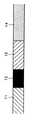
図1は、本発明の理解を助けるための一般的な連続増加記録モード時発生するリンキング体系を説明するための図面であって、旧データ、リンキング領域(32KBの場合)と新たなデータを示している。即ち、旧データ4が基本記録単位(図面ではECCブロック単位)を満たせきれずに記録が終われば、記録されない基本記録単位の残りの区間にはパディングデータ5をシンクマーク1以後の最初のセクターまで記録する。新たなデータ7を記録するために32KBに該当する連続増加記録のためのリンキング領域2にリンキングデータ6を記録した後再び新たな使用者データ7を記録している。
【0012】
一方、訂正されないエラーのようにウォッブル信号、LPP(Land Pre−Pit)信号のような基準信号が発生されない場合、即ち、大きい欠陥が複数のトラックにわたって存在すれば、このような欠陥領域をピックアップユニットが過ぎる場合全ての信号(ウォッブル信号、LPP信号など)が全く発生しない。このようになれば連続記録が不可能になり、欠陥領域の次の領域から記録されるべきなので連続増加記録モードと同じモードになる。
【0013】
付加的に、DVD−RWはグルーブトラックにデータが記録され、ランドトラックには物理的ECCブロック番号を示す情報がプリピット(pre-pit)で記録されており、これをLPP信号という。また、グルーブトラックは所定周波数でウォッブルされている。
【0014】
従って、一般的な連続増加記録モードまたは制限的重ね書き記録モードでのみ定義されたリンキング体系が前述したように欠陥領域の次でも発生するので新たなリンキング体系の定義が必要になる。しかし、DVD−RW規格には連続増加記録モードまたは制限的重ね書き記録モードの場合にだけリンキング体系が伴われることとだけ定義されているので、欠陥領域の次の領域で発生されるリンキング体系も定義されるべきである。
【0015】
このような欠陥領域の次のリンキングは一般的な連続増加記録モードまたは制限的重ね書き記録モードでのリンキングタイプとは区別させる必要がある。即ち、一般的な連続増加記録モード及び制限的重ね書きモードでのリンキングは、一回に記録する1回記録分に該当するデータを記録した後記録動作を止め、再び新たなデータを記録する時発生する。このようなリンキングは1回全面記録モードでは規定されていない。
【0016】
しかし、本発明で提案するリンキングは欠陥領域の次に示されることであって、まだ1回分に該当する記録が完全に遂行されない状態でも発生する。
図2は、本発明に係る欠陥領域処理方法の一例を説明するための図面である。検証時欠陥リストをRMD領域に登録した後欠陥領域の次にはリンキング領域が割当てられ、リンキング領域以後から使用者データを記録している。
【0017】
このRMD領域には検証時発見された欠陥リストだけでなく記録媒体を使用しながら発生した欠陥リストも貯蔵されるので、本発明は使用者データを記録する前または使用途中発生した欠陥領域に対するリストをRMD領域に貯蔵すると同時に一例として欠陥領域(ECCブロックまたはセクターになりうる)に属するセクターの先頭に存在するデータ識別(Data Identifier:DID)領域に欠陥領域の次の領域にリンキングが伴われることを示すリンキングタイプ情報を貯蔵する。以後、実際使用者データ記録時欠陥領域の次の領域はリンキング体系を適用した後使用者データを記録する。ここで、リンキングタイプ情報を付加情報と呼ぶことができ、欠陥領域の次の領域にデータを記録時リンキングが伴われることを示すリンキングタイプ情報は基本記録単位内に貯蔵されることができる。
【0018】
即ち、使用者データ4が記録される途中でRMDリストに登録されている欠陥領域3を発見すれば、その欠陥領域3には使用者データを記録せずに飛ばす。この時、欠陥領域3に対してはレーザー素子のような光源から出射される光パワーを記録に影響を与えないパワー、例えば再生パワー以下に低める。欠陥領域3の次のリンキング領域8にはリンキングデータ9が満たされ、再び新たなデータ7を記録し始める。この欠陥領域3の次に発生するリンキング領域8の大きさは2KBと32KB全て使用できるが、2KBを使用することがRTRW(Real Time
Read/Write)動作時有利な面がある。
【0019】
一方、本発明で提案するリンキングは検証時欠陥領域検出を通じて分かるため、検出された欠陥領域の次に所定のリンキング体系(2KBまたは32KB)に従って予めリンキングデータを記録しておくことができる。この時、図3に示したようなDID内のデータタイプ情報にはリンキングデータであることを示す情報を記録し、リンキングタイプ情報には欠陥領域の次に発生するリンキングであることを示す情報を記録する。
【0020】
欠陥領域直前の使用者領域で使用者データが基本記録単位を満たせきれない場合には残りの区間中ではパディングデータ(一例として00h)を記録するため、予めパディングデータを欠陥領域直前の基本記録単位領域に記録しておくことができる。このパディングデータ区間は実際使用者データを記録時重ね書きされることができる。
【0021】
このようにすれば検証後使用者データを記録する場合欠陥領域の次には予めリンキングデータが記録されているため、リンキング領域に継いで使用者データを記録することができる。従って、リンキングデータを記録するのにかかる時間を縮め、欠陥領域とリンキング領域の次にすぐ使用者データを記録するためリアルタイム記録に有利である。
【0022】
図3は、本発明に係るリンキングタイプ情報がセクター単位で4バイトに割当てられたDID領域内に貯蔵される一例を示し、データ識別情報はセクター情報とセクター番号よりなり、セクター情報にはセクターフォーマットタイプ、トラッキング方法、反射率、リンキングタイプ、領域タイプ、データタイプ、レイヤー番号がある。
【0023】
即ち、ビット位置b31のセクターフォーマットタイプ情報は下記のようにCLV(Constant Linear Velocity)かまたはZCLV(Zone Constant Linear Velocity)かを示している。
0b: CLV format type
1b: Zoned format type、specified for Rewritable discs
【0024】
ビット位置b30のトラッキング方法情報は下記のようにピットトラッキングかまたはグルーブトラッキングかを示している。
0b: Pit tracking
1b: Groove tracking、specified for Rewritable discs
ビット位置b29の反射率情報は下記のように反射率が40%を超過するかまたはその以下かを示している。
0b: If the reflectivity is greater than40%
1b: If there flectivity is less than or equal to40%
【0025】
ビット位置b27とb26の領域タイプ情報は下記のようにデータ領域、リードイン(lead-in)領域、リードアウト(lead-out)領域かまたは読出し専用ディスクのための中央領域かを示している。
00b: In the data area
01b: In the Lead-in area
10b: In the Lead-out area
11b: In the middle area of read-only discs
【0026】
ビット位置b25のデータタイプ情報は下記のように読出専用データかまたはリンキングデータかを示している。
0b: Read-only data
1b: Linking data
ビット位置b24のレイヤー番号情報は下記のように断面ディスクまたは両面ディスクでのレイヤー番号を示している。
0b: Layer0of dual layer discs or single layer discs
1b: Layer1of dual layer discs
【0027】
本発明ではセクター情報領域内に既存には予備されていたビットb28を用いてリンキングタイプ情報を下記のように定義してさらに記録する。
0b: Linking for incremental recording
1b: Linking after defective area
【0028】
即ち、リンキングタイプ情報が2進数で“0”であれば連続増加記録のためのリンキングで、“1”であれば欠陥領域の次のリンキングであることを示す。ここで、連続増加記録モードまたは制限的重ね書き記録モードで発生するリンキングタイプを第1リンキングタイプ(tpye I)とし、欠陥領域の次に発生するリンキングタイプを第2リンキングタイプ(type II)と命名できる。
【0029】
従って、一般的なリンキングタイプと本発明のリンキングタイプは区別され、このような欠陥領域の次のリンキングを示す情報をリンキングがおきるセクターのDID内に含めれば、そのセクターでリンキングがおきる場合、そのリンキングが連続増加記録または制限的重ね書き記録時発生したリンキングか、でなければ欠陥領域の次に発生したリンキングかが分かる。また、リンキングタイプ情報により一回に記録されるデータが連続的か、でなければ欠陥領域により分けられているかに対する情報も分かるので、ドライブではこのようなリンキングタイプ情報を高速データ処理に活用できる。
【0030】
本発明で提案する欠陥領域により伴われるリンキング体系はDVD−RWの全ての記録モード、即ち、1回全面記録モード、制限的重ね書き記録モード、連続増加記録モードの全てに適用されうる。
図4は本発明に係る欠陥領域処理方法の他の例を説明するための図面であって、参照符号11は旧データが記録された使用者データ領域で、12は欠陥ECCブロックで、13は欠陥ECCブロックの次にリンキング領域と同じ効果のために割当てられる所定数のECCブロックで、14は新たなデータが記録される使用者データ領域である。
【0031】
本発明では検証時検出された欠陥領域の次に割当てられた1ECCブロック(32KB)以上の領域を用いてリンキング体系を使用しなくても新たなデータの記録が再開される使用者データ領域を探索することができる。この時、欠陥領域の次の所定数のECCブロックはRMD領域に登録することもでき、予め決まった規則に従って欠陥領域の次には常に所定数のECCブロック以後に使用者データ領域が位置するということを定義することもできる。
【0032】
また、欠陥領域の次の所定数のECCブロック領域には高速探索のために予めリンキングデータ役割をするデータを記録しておくこともでき、所定のパターンを有する記録マークで記録しておくこともできる。これをテスト信号と呼ぶ。
検証後実際使用者データ記録時、信号が検出されない欠陥領域に会った後基準信号が検出されるかどうかを判断して基準信号が検出されれば、欠陥領域以後にリンキング領域と同じ効果を有するために割当てられたECCブロックであることを認識する。以後、欠陥領域の次の所定数のECCブロック以後の次の領域から残りの新たなデータを記録すればリアルタイム記録に有利である。基準信号はグルーブトラックはウォッブルされているのでウォッブル信号になる場合もあり、テスト信号になる場合もある。
【0033】
【発明の効果】
前述したように、本発明は連続増加記録または制限的重ね書き記録時発生するリンキング以外に欠陥領域の次に発生するリンキングを示すリンキングタイプ情報を用いて記録媒体上に大きい欠陥が発生して記録/再生に必要な基準信号が発生しなくても、欠陥領域の次の領域にリンキング体系を適用した後使用者データの記録を再開することによって使用者データの信頼性を高めることができ、より信頼性の高い再生を遂行することができる。
【0034】
また、本発明は検証時発見された欠陥領域の次の所定数のECCブロックに予めリンキングデータと同じ効果を有するテスト信号が記録されているため、検証後使用者データを記録する場合テスト信号またはグルーブトラックのウォッブル信号を用いて欠陥領域と所定数のECCブロックの次にすぐ継いで使用者データを記録するためリアルタイム記録に有利な長所がある。
【図面の簡単な説明】
【図1】 一般的な連続増加記録モード時に発生するリンキング体系を説明するための図面である。
【図2】 本発明に係る欠陥領域処理方法の一例を説明するための図面である。
【図3】 本発明に係るリンキングタイプ情報が貯蔵される一例のデータ識別DID領域の構造を示す図面である。
【図4】 本発明に係る欠陥領域処理方法の他の例を説明するための図面である。
【符号の説明】
1 シンクマーク
3 欠陥領域
4 使用者データ
7 新たなデータ
8 リンキング領域
9 リンキングデータ
11 旧データが記録された使用者データ領域
12 欠陥ECCブロック
13 所定数のECCブロック
14 新たなデータが記録される使用者データ領域[0001]
BACKGROUND OF THE INVENTION
The present invention relates to the field of optical recording media in which basic recording units are continuously in contact, and more particularly to a recording medium for storing linking type information indicating that linking is accompanied by a defect area and a defect area using this information. It relates to the processing method.
[0002]
[Prior art]
In the case of DVD-RW (Digital Versatile Disc Rewritable), the basic recording unit is a physical identifier (PID) area or a buffer field (required for precise control of the spindle motor) like DVD-RAM (Random Access Memory). It is necessary to make the recording start point of each basic unit accurate because it is continuously connected without being divided into margin areas allocated for correspondence). Here, the basic recording unit of the DVD-RAM can be a sector, and the basic recording unit of the DVD-RW can be an ECC (Error Correction Code) block.
[0003]
In the DVD-R (Recordable) and DVD-RW having the same physical format, the basic recording units are continuously connected as described above, so in the case of continuous increase recording, that is, the data transmission is instantaneously interrupted. When new data is recorded in succession to the previous data, a linking system is used in which a predetermined number of bytes (3 bytes as an example) are allocated to a margin area for the next recording start point. In addition, there are two types of linking areas applied at the time of such continuous increase recording: 2 kilobytes (KB) and 32 KB.
[0004]
However, in the case of DVD-RW, when a defective area list is registered in an RMD (Recording Management Data) area and actual user data is recorded next to the defective area registered in the defective area list, a limited overwriting is performed. Since the recording mode always involves linking like the continuous increase recording mode, the linking system is applied only to the continuous increase recording mode and the restrictive overwriting recording mode on the DVD-RW standard. It is not defined for the linking system that occurs.
[0005]
[Problems to be solved by the invention]
Accordingly, it is an object of the present invention to provide a recording medium that stores linking type information indicating linking that occurs next to a defective area in a recording medium in which basic recording units are in continuous contact.
Another object of the present invention is to provide a recording medium in which basic recording units are continuously in contact with a predetermined number of error correction code (ECC) blocks having the same effect as the linking area after the defective area. Is to provide.
[0006]
Still another object of the present invention is to provide a defect area in which user data is recorded after a predetermined linking system is applied next to the defect area in accordance with linking type information indicating that linking occurs after the defect area during recording. It is to provide a processing method.
It is still another object of the present invention to provide a defective area processing method for recording user data after a recording defective area and a predetermined number of error correction code (ECC) blocks subsequent thereto.
[0007]
[Means for Solving the Problems]
In order to achieve the above-described object, the recording medium of the present invention is a recording medium in which basic recording units are continuously in contact with each other in a defective area generated before recording user data or during use of the recording medium. Next, a linking area allocated according to a predetermined linking system, a defect management area in which a list of defect areas is registered, and additional information indicating that a predetermined linking system is applied next to the defect area are stored. It has a predetermined area.
[0008]
Also, the recording medium of the present invention is a recording medium in which basic recording units are continuously in contact with each other, one or more predetermined number of consecutive error correction codes (ECC) assigned next to a defective area discovered at the time of verification. And a defect management area in which information for a predetermined number of ECC blocks allocated immediately after the defect area is registered.
[0009]
The defect area processing method of the present invention is a method for processing a defect area on a recording medium having a defect area and a plurality of basic recording units that are in continuous contact with each other. (A) Verification before recording user data Detecting the defect area that occurs at the time and detecting the defect area that occurs during recording of the user data; and (b) registering the list of defect areas in the defect management area of the recording medium. And storing additional information indicating whether or not a predetermined linking system is applied to a linking area next to the defective area in a predetermined area of the recording medium.
The defect area processing method of the present invention is a method for processing a defect area before or during recording of user data on a recording medium having a plurality of basic recording units that are in continuous contact with each other. a) When the defective area is detected while recording the user data in the basic recording unit, a step of recording the user data after designating a predetermined linking system in the linking area next to the defective area; It is characterized by including.
[0010]
The defect area processing method of the present invention is a method for processing a defect area on a recording medium in which basic recording units are continuously in contact with each other. Allocating several error correction code (ECC) blocks, and registering a list of defective areas and information on a predetermined number of ECC blocks next to the defective areas in a defect management area.
[0011]
DETAILED DESCRIPTION OF THE INVENTION
Hereinafter, preferred embodiments of a recording medium for storing linking type information and a defect area processing method will be described with reference to the accompanying drawings.
FIG. 1 is a diagram for explaining a linking system generated in a general continuous increase recording mode for helping understanding of the present invention, and shows old data, a linking area (in the case of 32 KB), and new data. ing. That is, if the
[0012]
On the other hand, if a reference signal such as a wobble signal or LPP (Land Pre-Pit) signal is not generated like an uncorrected error, that is, if a large defect exists over a plurality of tracks, such a defective area is picked up by the pickup unit. When the period of time passes, all signals (wobble signal, LPP signal, etc.) are not generated at all. In this case, continuous recording becomes impossible, and since the recording should be performed from the area next to the defective area, the same mode as the continuous increase recording mode is set.
[0013]
In addition, in the DVD-RW, data is recorded on a groove track, and information indicating a physical ECC block number is recorded in a pre-pit on a land track, which is called an LPP signal. The groove track is wobbled at a predetermined frequency.
[0014]
Therefore, since the linking system defined only in the general continuous increase recording mode or the limited overwriting recording mode also occurs after the defect area as described above, it is necessary to define a new linking system. However, since the DVD-RW standard only defines that the linking system is accompanied only in the case of the continuous increase recording mode or the limited overwriting recording mode, the linking system generated in the area next to the defect area is also included. Should be defined.
[0015]
The next linking of such a defective area needs to be distinguished from the linking type in a general continuous recording mode or a limited overwriting recording mode. That is, the linking in the general continuous increase recording mode and the restrictive overwriting mode is performed when the data corresponding to one recording to be recorded at a time is recorded and then the recording operation is stopped and new data is recorded again. appear. Such linking is not defined in the one time full recording mode.
[0016]
However, the linking proposed in the present invention is shown next to the defect area, and occurs even in a state where the recording corresponding to one time is not completely performed yet.
FIG. 2 is a drawing for explaining an example of a defective area processing method according to the present invention. After registering the verification defect list in the RMD area, a linking area is allocated next to the defect area, and user data is recorded after the linking area.
[0017]
In this RMD area, not only a defect list discovered at the time of verification but also a defect list generated while using a recording medium is stored. Therefore, the present invention provides a list for a defect area generated before or during use of user data. As an example, the data identifier (DID) area existing at the head of the sector belonging to the defective area (which can be an ECC block or a sector) is linked to the area following the defective area. The linking type information indicating is stored. Thereafter, the user data is recorded in the area next to the defect area when the actual user data is recorded after the linking system is applied. Here, the linking type information can be referred to as additional information, and linking type information indicating that data is linked to the next area after the defect area can be stored in the basic recording unit.
[0018]
That is, if a
There is an advantageous aspect at the time of Read / Write operation.
[0019]
On the other hand, since the linking proposed in the present invention is known through detection of the defect area during verification, linking data can be recorded in advance according to a predetermined linking system (2 KB or 32 KB) after the detected defect area. At this time, information indicating that the data is linking data is recorded in the data type information in the DID as shown in FIG. 3, and information indicating that the linking occurs after the defect area is recorded in the linking type information. Record.
[0020]
If the user data cannot satisfy the basic recording unit in the user area immediately before the defective area, the padding data (for example, 00h) is recorded in the remaining section. Can be recorded in the area. This padding data section can be overwritten when actual user data is recorded.
[0021]
In this way, when the post-verification user data is recorded, since the linking data is recorded in advance after the defective area, the user data can be recorded following the linking area. Therefore, the time required for recording the linking data is shortened, and the user data is recorded immediately after the defect area and the linking area, which is advantageous for real-time recording.
[0022]
FIG. 3 shows an example in which the linking type information according to the present invention is stored in a DID area allocated to 4 bytes in a sector unit. The data identification information includes sector information and a sector number. The sector information includes a sector format. Type, tracking method, reflectance, linking type, region type, data type, and layer number.
[0023]
That is, the sector format type information at the bit position b31 indicates whether it is CLV (Constant Linear Velocity) or ZCLV (Zone Constant Linear Velocity) as described below.
0b: CLV format type
1b: Zoned format type, specified for Rewritable discs
[0024]
The tracking method information at the bit position b30 indicates pit tracking or groove tracking as described below.
0b: Pit tracking
1b: Groove tracking, specified for Rewritable discs
The reflectivity information at bit position b29 indicates whether the reflectivity exceeds 40% or less as described below.
0b: If the reflectivity is greater than 40%
1b: If there flectivity is less than or equal to 40%
[0025]
The area type information at bit positions b27 and b26 indicates whether it is a data area, a lead-in area, a lead-out area or a central area for a read-only disc as follows.
00b: In the data area
01b: In the Lead-in area
10b: In the Lead-out area
11b: In the middle area of read-only discs
[0026]
The data type information at bit position b25 indicates whether it is read-only data or linking data as described below.
0b: Read-only data
1b: Linking data
The layer number information at bit position b24 indicates the layer number on the cross-section disc or double-sided disc as follows.
0b: Layer0of dual layer discs or single layer discs
1b:
[0027]
In the present invention, the linking type information is further defined and recorded as follows using the bit b28 which has been reserved in the sector information area.
0b: Linking for incremental recording
1b: Linking after defective area
[0028]
That is, if the linking type information is binary number “0”, it indicates linking for continuous increase recording, and if it is “1”, it indicates the next linking of the defective area. Here, the linking type that occurs in the continuous incremental recording mode or the limited overwriting recording mode is the first linking type (tpye I), and the linking type that occurs after the defective area is the second linking type (type II). it can.
[0029]
Therefore, the general linking type is distinguished from the linking type of the present invention, and if information indicating the next linking of such a defective area is included in the DID of the sector where the linking occurs, It can be seen whether linking occurred during continuous incremental recording or limited overwriting recording, or otherwise linking that occurred after the defective area. In addition, since it is also possible to know whether the data recorded at one time is continuous or otherwise divided by the defective area according to the linking type information, the linking type information can be used for high-speed data processing in the drive.
[0030]
The linking system accompanied by the defective area proposed in the present invention can be applied to all the recording modes of DVD-RW, that is, all the single recording mode, limited overwriting recording mode, and continuous incremental recording mode.
FIG. 4 is a diagram for explaining another example of the defective area processing method according to the present invention.
[0031]
In the present invention, a user data area in which recording of new data is resumed without using a linking system using an area of 1 ECC block (32 KB) or more allocated next to a defective area detected at the time of verification is searched. can do. At this time, the predetermined number of ECC blocks next to the defective area can be registered in the RMD area, and the user data area is always located after the predetermined number of ECC blocks after the defective area according to a predetermined rule. Can also be defined.
[0032]
In addition, data serving as linking data can be recorded in advance for a high-speed search in a predetermined number of ECC block areas next to the defective area, or can be recorded with recording marks having a predetermined pattern. it can. This is called a test signal.
When recording the actual user data after the verification, if the reference signal is detected by determining whether the reference signal is detected after meeting the defective area where no signal is detected, the same effect as the linking area after the defective area is obtained. It is recognized that the ECC block is allocated for the purpose. Thereafter, if the remaining new data is recorded from the next area after the predetermined number of ECC blocks next to the defective area, it is advantageous for real-time recording. Since the groove track is wobbled, the reference signal may be a wobble signal or a test signal.
[0033]
【The invention's effect】
As described above, the present invention uses the linking type information indicating the linking that occurs next to the defective area in addition to the linking that occurs during continuous incremental recording or limited overwriting recording. / Even if the reference signal required for playback is not generated, the reliability of the user data can be improved by resuming the recording of the user data after applying the linking system to the next area of the defective area. Reliable reproduction can be performed.
[0034]
In the present invention, since a test signal having the same effect as the linking data is recorded in advance in a predetermined number of ECC blocks next to the defective area discovered at the time of verification, the test signal or Since user data is recorded immediately after a defective area and a predetermined number of ECC blocks by using a wobble signal of a groove track, there is an advantage advantageous for real-time recording.
[Brief description of the drawings]
FIG. 1 is a diagram for explaining a linking system that occurs in a general continuous increase recording mode.
FIG. 2 is a drawing for explaining an example of a defective area processing method according to the present invention.
FIG. 3 is a view illustrating a structure of an example data identification DID area in which linking type information according to the present invention is stored;
FIG. 4 is a drawing for explaining another example of the defective area processing method according to the present invention.
[Explanation of symbols]
DESCRIPTION OF
Claims (23)
Translated fromJapanese(a)使用者データを記録する前検証時発生する前記欠陥領域を検出し、かつ、前記使用者データの記録中に発生する前記欠陥領域を検出する段階と、
(b)前記欠陥領域のリストを前記光記録媒体の欠陥管理領域に登録し、かつ、前記欠陥領域の直後に所定のリンキング体系に従ってリンキング領域が割り当てられるかどうかを示す付加情報を光記録媒体の所定の領域に貯蔵する段階とを含む方法。In the defect area processing method on the optical recording medium inwhich the basic recording units are in continuous contact ,
(A) detecting the defective area that occurs during verification before recording user data, and detecting the defective area that occurs during recording of the user data;
(B) Registering the list of defect areas in the defect management area of theoptical recording medium, and adding additional information indicating whether a linking area is allocatedaccording to a predetermined linking system immediately after the defect area of theoptical recording medium Storing in a predetermined area.
(d)前記付加情報が、前記欠陥領域の直後にリンキング領域が割り当てられることを示せば、前記リンキング領域の直後の領域内に前記使用者データを記録する段階とをさらに含む請求項1に記載の方法。(C) Checking the additional information if the defect area registered in the defect management area is found when the user data is recorded in thebasic recording unit;
2. The method of claim 1, further comprising: (d) recording the user data inan areaimmediately after the linking area if the additional information indicatesthat a linking area is allocatedimmediately after the defect area. the method of.
(a)前記基本記録単位内に使用者データを記録する中前記欠陥領域が検出されると、前記欠陥領域の直後に所定のリンキング体系に従ってリンキング領域を割り当てた後前記使用者データを記録する段階を含む方法。In a method for processing a defective area before recording user data or recording user data on anoptical recording medium having a plurality ofbasic recording units that are in continuous contact with each other,
(A) recording the user data after allocating a linking areaaccording to a predetermined linking system immediately after the defective area when the defective area is detected while recording the user data in thebasic recording unit; Including methods.
(c)検証中前記リンキング領域に予めリンキングデータを記録する段階とをさらに含む請求項14に記載の方法。(B) assigning the linking areaimmediately after the defective area during pre-verification of recording the user data;
15. The method of claim 14, further comprising: (c) pre-recording linking data in the linking area during verification.
(a)検証中検出した前記欠陥領域の直後に所定の数のエラー訂正コード(ECC)ブロックを割り当てる段階と、
(b)前記欠陥領域のリストと、前記欠陥領域の直後の前記所定の数のECCブロック上の情報とを前記光記録媒体の欠陥管理領域に登録する段階と、
(c)前記欠陥領域の直後の前記所定の数のECCブロックに、所定の試験信号又はウォブル信号を基準信号として記録する段階と、
(d)検出された前記欠陥領域の直後の前記所定の数のECCブロックに前記基準信号が検出された場合に、検証後、前記欠陥領域の直後の前記所定の数のECCブロックの直後に前記使用者データを記録する段階とを含むことを特徴とする方法。In the defect area processing method on the optical recording medium inwhich the basic recording units are in continuous contact ,
(A) assigning a predetermined number of error correction code (ECC) blocksimmediately after the defective area detected during verification;
(B) registering the list of defect areas and information on the predetermined number of ECC blocksimmediately after the defect areas in the defect management area of theoptical recording medium;
(C) recording a predetermined test signal or wobble signal as a reference signal in the predetermined number of ECC blocks immediately after the defective area;
(D) When the reference signal is detected in the predetermined number of ECC blocksimmediately after the detected defective area, after the verification, immediately after the predetermined number of ECC blocks immediatelyafter the defective area Recording the user data.
(a)使用者データを記録する前検証時発生する前記欠陥領域を検出する段階と、
(b)前記欠陥領域のリストを前記光記録媒体の欠陥管理領域に登録し、かつ、前記欠陥領域の直後に所定のリンキング体系に従ってリンキング領域を割り当てる段階とを含み、
前記光記録媒体は、DVD−RWディスクであり、前記欠陥管理領域は、光記録媒体の記録管理データ領域であることを特徴とする方法。In the defect area processing method on the optical recording medium inwhich the basic recording units are in continuous contact ,
(A) detecting the defective area generated at the time of verification before recording user data;
(B) registering the list of defect areas in a defect management area of theoptical recording medium, and allocating a linking areaaccording to a predetermined linking system immediately after the defect area,
The method according to claim 1, wherein theoptical recording medium is a DVD-RW disc, and the defect management area is a recording management data area of theoptical recording medium.
Applications Claiming Priority (6)
| Application Number | Priority Date | Filing Date | Title |
|---|---|---|---|
| KR19990016462 | 1999-05-08 | ||
| KR19990016973 | 1999-05-12 | ||
| KR199916462 | 1999-06-24 | ||
| KR199923947 | 1999-06-24 | ||
| KR1019990023947AKR100544175B1 (en) | 1999-05-08 | 1999-06-24 | Recording medium and defect area processing method for storing linking type information |
| KR199916973 | 1999-06-24 |
Related Parent Applications (1)
| Application Number | Title | Priority Date | Filing Date |
|---|---|---|---|
| JP2000132944ADivisionJP3868712B2 (en) | 1999-05-08 | 2000-05-01 | Recording medium for storing linking type information and defect area processing method using this information |
Publications (2)
| Publication Number | Publication Date |
|---|---|
| JP2001357625A JP2001357625A (en) | 2001-12-26 |
| JP3868761B2true JP3868761B2 (en) | 2007-01-17 |
Family
ID=36592740
Family Applications (3)
| Application Number | Title | Priority Date | Filing Date |
|---|---|---|---|
| JP2000132944AExpired - Fee RelatedJP3868712B2 (en) | 1999-05-08 | 2000-05-01 | Recording medium for storing linking type information and defect area processing method using this information |
| JP2001137873AExpired - LifetimeJP3868760B2 (en) | 1999-05-08 | 2001-05-08 | Device for recording and / or reproducing linking type information |
| JP2001137874AExpired - Fee RelatedJP3868761B2 (en) | 1999-05-08 | 2001-05-08 | Defect region processing method using linking type information |
Family Applications Before (2)
| Application Number | Title | Priority Date | Filing Date |
|---|---|---|---|
| JP2000132944AExpired - Fee RelatedJP3868712B2 (en) | 1999-05-08 | 2000-05-01 | Recording medium for storing linking type information and defect area processing method using this information |
| JP2001137873AExpired - LifetimeJP3868760B2 (en) | 1999-05-08 | 2001-05-08 | Device for recording and / or reproducing linking type information |
Country Status (12)
| Country | Link |
|---|---|
| US (8) | US6785206B1 (en) |
| EP (4) | EP1258883B1 (en) |
| JP (3) | JP3868712B2 (en) |
| KR (1) | KR100544175B1 (en) |
| CN (4) | CN1149567C (en) |
| BR (2) | BRPI0003048B1 (en) |
| DE (3) | DE60035614T2 (en) |
| ID (1) | ID26497A (en) |
| MY (3) | MY125268A (en) |
| RU (3) | RU2238596C2 (en) |
| SG (4) | SG153642A1 (en) |
| TW (3) | TWI234138B (en) |
Families Citing this family (70)
| Publication number | Priority date | Publication date | Assignee | Title |
|---|---|---|---|---|
| KR100601598B1 (en)* | 1998-06-15 | 2006-07-14 | 삼성전자주식회사 | Recording media that store write-protected information and record-protection methods |
| US6765853B1 (en) | 1998-06-15 | 2004-07-20 | Samsung Electronics Co., Ltd. | Recording medium for storing write protection information and write protection method thereof |
| KR100544175B1 (en) | 1999-05-08 | 2006-01-23 | 삼성전자주식회사 | Recording medium and defect area processing method for storing linking type information |
| KR100374606B1 (en)* | 2000-11-20 | 2003-03-04 | 삼성전자주식회사 | A recording medium storing link information, apparatus and method for linking data |
| KR100378165B1 (en)* | 2000-11-27 | 2003-03-29 | 삼성전자주식회사 | Method for overwriting data in linking loss area |
| KR100475604B1 (en)* | 2001-03-09 | 2005-03-10 | 엘지전자 주식회사 | Read only optical disc, and method for reproducing a data in read only optical disc player |
| CN1488141A (en)* | 2001-05-09 | 2004-04-07 | 皇家菲利浦电子有限公司 | A method of and a system to play a media file |
| US20030058762A1 (en)* | 2001-09-26 | 2003-03-27 | Schultz Mark Alan | Defect detection of recordable storage media |
| KR100576163B1 (en)* | 2002-12-13 | 2006-05-03 | 엘지전자 주식회사 | Linking Area Data Recording Method of High Density Playback-Only Optical Discs, and Consequently High Density Playback-Only Optical Discs |
| US7123556B2 (en)* | 2002-01-22 | 2006-10-17 | Matsushita Electric Industrial Co., Ltd. | Multi-layered information recording medium with spare defect management areas |
| TWI244078B (en)* | 2002-03-29 | 2005-11-21 | Samsung Electronics Co Ltd | Optical disk and method of recording data to the same |
| KR100878522B1 (en)* | 2002-03-29 | 2009-01-13 | 삼성전자주식회사 | Optical disc and recording method of optical disc |
| US6999390B2 (en) | 2002-05-06 | 2006-02-14 | Samsung Electronics Co., Ltd. | Optical disk and method of recording data in the same |
| US7145861B2 (en) | 2002-05-06 | 2006-12-05 | Samsung Electronics Co., Ltd. | Apparatus for recording and/or reproducing optical disk |
| JP3875912B2 (en)* | 2002-05-09 | 2007-01-31 | ソニー株式会社 | Optical disc recording method, optical disc recording apparatus, and information recording medium |
| KR100727917B1 (en)* | 2002-05-20 | 2007-06-14 | 삼성전자주식회사 | Optical disc and recording / playback method of optical disc |
| CN1331122C (en)* | 2002-05-20 | 2007-08-08 | 三星电子株式会社 | Optical disc and method for recording data on the same |
| JP3858766B2 (en)* | 2002-06-04 | 2006-12-20 | ソニー株式会社 | Optical disc recording method, optical disc recording apparatus, and information recording medium |
| RU2302043C2 (en)* | 2002-06-05 | 2007-06-27 | Эл Джи Электроникс Инк. | Linking zone structure made on carrier only for reading high density records, method and device for manufacturing and reading the carrier |
| TWI348692B (en)* | 2002-06-05 | 2011-09-11 | Lg Electronics Inc | High-density optical disc, method and apparatus for recording and reproducing encrypted data thereon |
| EP1571665A3 (en)* | 2002-06-05 | 2010-04-07 | Lg Electronics Inc. | Recording medium with a linking area including dummy data thereon and apparatus and methods for forming, recording, and reproducing the recording medium |
| CN100447880C (en)* | 2002-06-21 | 2008-12-31 | Lg电子株式会社 | Recording medium having a data structure for managing reproduction of video data recorded thereon |
| EP1543507A1 (en) | 2002-09-26 | 2005-06-22 | LG Electronics Inc. | Method for managing defective area on write-once optical recording medium, and optical recording medium using the same |
| AU2003264977B2 (en) | 2002-09-26 | 2009-03-26 | Lg Electronics Inc. | Optical disc, method and apparatus for managing a defective area on an optical disc of write once type |
| KR20040027259A (en) | 2002-09-26 | 2004-04-01 | 엘지전자 주식회사 | Method for managing a defect area on optical disc write once |
| KR20040028469A (en) | 2002-09-30 | 2004-04-03 | 엘지전자 주식회사 | Method for managing a defect area on optical disc write once |
| US7233550B2 (en) | 2002-09-30 | 2007-06-19 | Lg Electronics Inc. | Write-once optical disc, and method and apparatus for recording management information on write-once optical disc |
| JP3867038B2 (en)* | 2002-10-23 | 2007-01-10 | 株式会社リコー | Information recording apparatus, information recording method, program, and recording medium |
| JP2004185650A (en)* | 2002-11-29 | 2004-07-02 | Toshiba Corp | Data recording device and data recording method |
| WO2004053874A1 (en) | 2002-12-11 | 2004-06-24 | Lg Electronics Inc. | Method of managing overwrite and method of recording management information on an optical disc write once |
| WO2004053872A1 (en) | 2002-12-11 | 2004-06-24 | Lg Electronics Inc. | Method and apparatus for managing overwrite on an optical disc write once |
| US7355934B2 (en) | 2003-01-27 | 2008-04-08 | Lg Electronics Inc. | Optical disc of write once type, method, and apparatus for managing defect information on the optical disc |
| US7372788B2 (en) | 2003-01-14 | 2008-05-13 | Lg Electronics Inc. | Method for managing defective area on write-once optical recording medium, and optical recording medium using the same |
| TWI334595B (en) | 2003-01-27 | 2010-12-11 | Lg Electronics Inc | Optical disc, method and apparatus for managing a defective area on an optical disc |
| US20040160799A1 (en) | 2003-02-17 | 2004-08-19 | Park Yong Cheol | Write-once optical disc, and method and apparatus for allocating spare area on write-once optical disc |
| US7499383B2 (en) | 2003-02-21 | 2009-03-03 | Lg Electronics Inc. | Write-once optical disc and method for managing spare area thereof |
| US7643390B2 (en) | 2003-02-21 | 2010-01-05 | Lg Electronics Inc. | Write-once optical recording medium and defect management information management method thereof |
| US7477581B2 (en)* | 2003-02-25 | 2009-01-13 | Lg Electronics Inc. | Defect management method for optical recording medium and optical recording medium using the same |
| US7188271B2 (en) | 2003-02-25 | 2007-03-06 | Lg Electronics Inc. | Write-once optical disc, and method and apparatus for recording management information on write-once optical disc |
| AU2003282449A1 (en) | 2003-03-04 | 2004-09-28 | Lg Electronics Inc. | Method for recording on optical recording medium and apparatus using the same |
| JP4870554B2 (en)* | 2003-03-13 | 2012-02-08 | サムスン エレクトロニクス カンパニー リミテッド | Write-once disc capable of data area management, data area management method of write-once disc, data recording apparatus, data reproduction method and apparatus thereof |
| RU2005127337A (en)* | 2003-03-13 | 2006-02-10 | Самсунг Электроникс Ко. Лтд. (Kr) | ONE-TIME RECORDED DISC, METHOD FOR DISTRIBUTING A DATA AREA FOR ONE-RECORDED DISC, DEVICE AND METHOD FOR PLAYING DATA FROM SUCH A DISC |
| TWI405196B (en) | 2003-03-13 | 2013-08-11 | Lg Electronics Inc | Optical recording medium and defective area management method and apparatus for write-once recording medium |
| JP3594243B1 (en)* | 2003-03-25 | 2004-11-24 | 株式会社リコー | Optical information recording method, optical information recording device, information processing device, optical information recording medium |
| KR100677113B1 (en)* | 2003-04-30 | 2007-02-01 | 삼성전자주식회사 | A method of recording a temporary defect list in a recording information storage medium once, the reproduction method thereof, the recording and / or reproducing apparatus, and the once recording information storage medium |
| MXPA05012044A (en) | 2003-05-09 | 2006-02-03 | Lg Electronics Inc | Write once optical disc, and method and apparatus for recovering disc management information from the write once optical disc. |
| BRPI0410198A (en) | 2003-05-09 | 2006-05-23 | Lg Electronics Inc | physical recording medium, method of managing disk management information, method of retrieving management information from physical recording medium, apparatus for managing disk management information on physical recording medium, and apparatus for retrieving management information from of the physical recording medium |
| KR101049135B1 (en) | 2003-07-14 | 2011-07-14 | 엘지전자 주식회사 | Write-once optical disc, method and apparatus for recording management information on write-once optical disc |
| KR101014703B1 (en) | 2003-07-15 | 2011-02-21 | 엘지전자 주식회사 | Method of managing defect area of optical disc, recording method of optical disc and recording / playback apparatus |
| KR20050009031A (en) | 2003-07-15 | 2005-01-24 | 엘지전자 주식회사 | Method for recording management information on optical disc write once |
| MXPA06001429A (en) | 2003-08-05 | 2006-05-19 | Lg Electronics Inc | Write-once optical disc, and method and apparatus for recording/reproducing management information on/from optical disc. |
| US7313065B2 (en) | 2003-08-05 | 2007-12-25 | Lg Electronics Inc. | Write-once optical disc, and method and apparatus for recording/reproducing management information on/from optical disc |
| JP2007505432A (en) | 2003-09-08 | 2007-03-08 | エルジー エレクトロニクス インコーポレーテッド | Write-once optical disc, and method and apparatus for recording management information on the optical disc |
| CA2537895A1 (en) | 2003-09-08 | 2005-03-17 | Lg Electronics Inc. | Write-once optical disc, and method and apparatus for recording management information thereon |
| CA2537888C (en) | 2003-09-08 | 2015-03-03 | Lg Electronics Inc. | Write-once optical disc and method for recording management information thereon |
| CN1331147C (en)* | 2003-09-12 | 2007-08-08 | 联想(北京)有限公司 | A disk storage method |
| KR100964685B1 (en) | 2003-10-20 | 2010-06-21 | 엘지전자 주식회사 | Recordable reproducing method and recording / reproducing apparatus for optical disc and recordable disc once |
| WO2005062303A1 (en)* | 2003-12-19 | 2005-07-07 | Koninklijke Philips Electronics N.V. | Optical disc for storing both data requiring defect management and real-time av data |
| US20050167430A1 (en)* | 2004-02-03 | 2005-08-04 | Sonoco Development, Inc. | Double rib overcap for a container with a removable membrane |
| KR100667753B1 (en)* | 2004-02-28 | 2007-01-11 | 삼성전자주식회사 | Information storage medium, method and apparatus for recording data |
| TWI247281B (en)* | 2004-03-31 | 2006-01-11 | Mediatek Inc | Method of determining defect detection mode for optical storage device |
| KR101049117B1 (en) | 2004-06-08 | 2011-07-14 | 엘지전자 주식회사 | Method and apparatus for recording management information on optical write once disc |
| KR100667764B1 (en)* | 2004-10-08 | 2007-01-12 | 삼성전자주식회사 | Optical recording medium, recording / reproducing method and recording / reproducing apparatus |
| KR20060081323A (en)* | 2005-01-07 | 2006-07-12 | 엘지전자 주식회사 | Record media playback method and playback device using local storage |
| JP2006252715A (en)* | 2005-03-14 | 2006-09-21 | Funai Electric Co Ltd | Optical disk recording/reproducing device |
| US20070050668A1 (en)* | 2005-09-01 | 2007-03-01 | Micron Technology, Inc. | Test mode to force generation of all possible correction codes in an ECC memory |
| KR20070058291A (en) | 2005-12-02 | 2007-06-08 | 엘지전자 주식회사 | Recording medium, method and recording device for recording management information of recording medium |
| KR100754228B1 (en)* | 2007-01-22 | 2007-09-03 | 삼성전자주식회사 | Optical disc and recording / playback method of optical disc |
| JP2009064540A (en)* | 2007-08-10 | 2009-03-26 | Hitachi Ltd | Optical disc apparatus, optical disc recording method and reproducing method |
| KR101044533B1 (en)* | 2009-06-29 | 2011-06-27 | 주식회사 하이닉스반도체 | Nonvolatile memory device and its copyback program method |
Family Cites Families (102)
| Publication number | Priority date | Publication date | Assignee | Title |
|---|---|---|---|---|
| US4498146A (en) | 1982-07-30 | 1985-02-05 | At&T Bell Laboratories | Management of defects in storage media |
| JP2590071B2 (en)* | 1986-08-29 | 1997-03-12 | 株式会社東芝 | Information processing device |
| US5095344A (en)* | 1988-06-08 | 1992-03-10 | Eliyahou Harari | Highly compact eprom and flash eeprom devices |
| US5043940A (en)* | 1988-06-08 | 1991-08-27 | Eliyahou Harari | Flash EEPROM memory systems having multistate storage cells |
| DE69025781T2 (en) | 1989-01-20 | 1996-10-17 | Sony Corp | Disk recording and playback device |
| JP2848528B2 (en)* | 1989-02-16 | 1999-01-20 | オリンパス光学工業株式会社 | Optical disk drive |
| US5070032A (en)* | 1989-03-15 | 1991-12-03 | Sundisk Corporation | Method of making dense flash eeprom semiconductor memory structures |
| US5172338B1 (en)* | 1989-04-13 | 1997-07-08 | Sandisk Corp | Multi-state eeprom read and write circuits and techniques |
| EP0935255A2 (en)* | 1989-04-13 | 1999-08-11 | SanDisk Corporation | Flash EEPROM system |
| JP3141241B2 (en)* | 1990-08-24 | 2001-03-05 | ソニー株式会社 | Disk recording device and disk reproducing device |
| JP3021029B2 (en)* | 1990-11-20 | 2000-03-15 | シャープ株式会社 | Information access method for magneto-optical recording medium |
| US5343063A (en)* | 1990-12-18 | 1994-08-30 | Sundisk Corporation | Dense vertical programmable read only memory cell structure and processes for making them |
| US5274646A (en)* | 1991-04-17 | 1993-12-28 | International Business Machines Corporation | Excessive error correction control |
| US6222762B1 (en)* | 1992-01-14 | 2001-04-24 | Sandisk Corporation | Multi-state memory |
| US5313421A (en)* | 1992-01-14 | 1994-05-17 | Sundisk Corporation | EEPROM with split gate source side injection |
| US5315421A (en)* | 1992-04-28 | 1994-05-24 | Matsushita Electric Industrial Co., Ltd. | Rubbing apparatus including double refraction phase difference measuring means and manufacturing method for liquid crystal display device |
| US5532962A (en)* | 1992-05-20 | 1996-07-02 | Sandisk Corporation | Soft errors handling in EEPROM devices |
| JP3528179B2 (en)* | 1992-07-31 | 2004-05-17 | ソニー株式会社 | Recording device and recording method |
| US5428621A (en)* | 1992-09-21 | 1995-06-27 | Sundisk Corporation | Latent defect handling in EEPROM devices |
| JP3105092B2 (en)* | 1992-10-06 | 2000-10-30 | 株式会社東芝 | Semiconductor memory device |
| US5404485A (en)* | 1993-03-08 | 1995-04-04 | M-Systems Flash Disk Pioneers Ltd. | Flash file system |
| JPH06266596A (en)* | 1993-03-11 | 1994-09-22 | Hitachi Ltd | Flash memory file storage device and information processor |
| JP3078946B2 (en)* | 1993-03-11 | 2000-08-21 | インターナショナル・ビジネス・マシーンズ・コーポレ−ション | Managing method of batch erase nonvolatile memory and semiconductor disk device |
| US5367484A (en)* | 1993-04-01 | 1994-11-22 | Microchip Technology Incorporated | Programmable high endurance block for EEPROM device |
| KR970008188B1 (en)* | 1993-04-08 | 1997-05-21 | 가부시끼가이샤 히다찌세이사꾸쇼 | Flash memory control method and information processing device using the same |
| JPH06314174A (en) | 1993-04-28 | 1994-11-08 | Matsushita Electric Ind Co Ltd | Information recording medium and information recording / reproducing apparatus |
| US5555204A (en)* | 1993-06-29 | 1996-09-10 | Kabushiki Kaisha Toshiba | Non-volatile semiconductor memory device |
| JP2922116B2 (en)* | 1993-09-02 | 1999-07-19 | 株式会社東芝 | Semiconductor storage device |
| KR0169267B1 (en)* | 1993-09-21 | 1999-02-01 | 사토 후미오 | Nonvolatile Semiconductor Memory |
| US5661053A (en)* | 1994-05-25 | 1997-08-26 | Sandisk Corporation | Method of making dense flash EEPROM cell array and peripheral supporting circuits formed in deposited field oxide with the use of spacers |
| US5691967A (en)* | 1994-09-20 | 1997-11-25 | Sony Corporation | Recording or reproducing apparatus having a spindle servo control runaway prevent feature |
| JP2915307B2 (en)* | 1994-12-19 | 1999-07-05 | 株式会社日立製作所 | Information recording control method for optical disk |
| CA2169131C (en) | 1995-02-28 | 2004-08-10 | Fabrizio Caffarelli | Compact disc recording system and method |
| JP3153730B2 (en)* | 1995-05-16 | 2001-04-09 | 株式会社東芝 | Nonvolatile semiconductor memory device |
| US5907856A (en)* | 1995-07-31 | 1999-05-25 | Lexar Media, Inc. | Moving sectors within a block of information in a flash memory mass storage architecture |
| JP3527572B2 (en) | 1995-08-19 | 2004-05-17 | 株式会社リコー | CD-E writing system device |
| JP3604466B2 (en)* | 1995-09-13 | 2004-12-22 | 株式会社ルネサステクノロジ | Flash disk card |
| US6125435A (en)* | 1995-09-13 | 2000-09-26 | Lexar Media, Inc. | Alignment of cluster address to block addresses within a semiconductor non-volatile mass storage memory |
| US5623470A (en) | 1995-12-28 | 1997-04-22 | International Business Machines Corporation | Reallocation of defective recording areas on CD-R or CD-E media |
| US5966114A (en)* | 1996-02-20 | 1999-10-12 | Sanyo Electric Co., Ltd. | Data processor having graphical user interface and recording medium therefor |
| JP3614173B2 (en)* | 1996-02-29 | 2005-01-26 | 株式会社ルネサステクノロジ | Semiconductor memory device with partially defective memory |
| JPH09237421A (en)* | 1996-03-01 | 1997-09-09 | Sony Corp | Recording and reproducing device and method |
| US5903495A (en)* | 1996-03-18 | 1999-05-11 | Kabushiki Kaisha Toshiba | Semiconductor device and memory system |
| JP2848809B2 (en)* | 1996-03-25 | 1999-01-20 | 株式会社東芝 | Replacement processing method |
| JP4557272B2 (en) | 1996-03-29 | 2010-10-06 | ソニー株式会社 | Recording / reproducing apparatus and method |
| JP3824701B2 (en) | 1996-04-01 | 2006-09-20 | パイオニア株式会社 | Information recording method and apparatus |
| US5768192A (en)* | 1996-07-23 | 1998-06-16 | Saifun Semiconductors, Ltd. | Non-volatile semiconductor memory cell utilizing asymmetrical charge trapping |
| US5798968A (en)* | 1996-09-24 | 1998-08-25 | Sandisk Corporation | Plane decode/virtual sector architecture |
| US5860124A (en)* | 1996-09-30 | 1999-01-12 | Intel Corporation | Method for performing a continuous over-write of a file in nonvolatile memory |
| JPH10125006A (en)* | 1996-10-18 | 1998-05-15 | Sony Corp | Signal recorder and signal recording method |
| JP3845849B2 (en)* | 1996-10-18 | 2006-11-15 | ソニー株式会社 | Recording apparatus, recording method, and recording medium |
| US5890192A (en)* | 1996-11-05 | 1999-03-30 | Sandisk Corporation | Concurrent write of multiple chunks of data into multiple subarrays of flash EEPROM |
| JPH10269751A (en) | 1997-03-24 | 1998-10-09 | Ricoh Co Ltd | Information recording / reproducing device |
| US5822245A (en)* | 1997-03-26 | 1998-10-13 | Atmel Corporation | Dual buffer flash memory architecture with multiple operating modes |
| US6034897A (en)* | 1999-04-01 | 2000-03-07 | Lexar Media, Inc. | Space management for managing high capacity nonvolatile memory |
| JP4144054B2 (en) | 1997-07-24 | 2008-09-03 | ソニー株式会社 | Optical disc recording method |
| US5930167A (en)* | 1997-07-30 | 1999-07-27 | Sandisk Corporation | Multi-state non-volatile flash memory capable of being its own two state write cache |
| US6768165B1 (en)* | 1997-08-01 | 2004-07-27 | Saifun Semiconductors Ltd. | Two bit non-volatile electrically erasable and programmable semiconductor memory cell utilizing asymmetrical charge trapping |
| US6021463A (en)* | 1997-09-02 | 2000-02-01 | International Business Machines Corporation | Method and means for efficiently managing update writes and fault tolerance in redundancy groups of addressable ECC-coded sectors in a DASD storage subsystem |
| US5909449A (en)* | 1997-09-08 | 1999-06-01 | Invox Technology | Multibit-per-cell non-volatile memory with error detection and correction |
| JP3855390B2 (en) | 1997-09-16 | 2006-12-06 | ソニー株式会社 | Recording apparatus, recording method, and disk-shaped recording medium |
| US5937425A (en)* | 1997-10-16 | 1999-08-10 | M-Systems Flash Disk Pioneers Ltd. | Flash file system optimized for page-mode flash technologies |
| JPH11203191A (en)* | 1997-11-13 | 1999-07-30 | Seiko Epson Corp | Nonvolatile storage device, method of controlling nonvolatile storage device, and information recording medium recording program for controlling nonvolatile storage device |
| CN1249585C (en)* | 1997-12-16 | 2006-04-05 | Tdk株式会社 | Flash memory system |
| WO1999032977A1 (en)* | 1997-12-22 | 1999-07-01 | Tdk Corporation | Flash memory system |
| JPH11213626A (en)* | 1998-01-21 | 1999-08-06 | Toshiba Corp | Data recording medium, data recording device, and data reproducing device |
| US6040997A (en)* | 1998-03-25 | 2000-03-21 | Lexar Media, Inc. | Flash memory leveling architecture having no external latch |
| RU2192673C2 (en)* | 1998-04-20 | 2002-11-10 | Самсунг Электроникс Ко., Лтд. | Record medium for data storage (alternatives), method for handling defects, and method for real- time data recording |
| KR100274400B1 (en)* | 1998-05-09 | 2000-12-15 | 구자홍 | Manufacturing method, recording / reproducing method and apparatus thereof of optical recording medium having differential free space |
| JP2000137948A (en) | 1998-10-30 | 2000-05-16 | Victor Co Of Japan Ltd | Recording medium, recording method and device, and reproducing method and device |
| US6490649B2 (en)* | 1998-11-10 | 2002-12-03 | Lexar Media, Inc. | Memory device |
| AU1729100A (en)* | 1998-11-17 | 2000-06-05 | Lexar Media, Inc. | Method and apparatus for memory control circuit |
| JP2000215452A (en)* | 1999-01-19 | 2000-08-04 | Victor Co Of Japan Ltd | Optical disk recording/reproducing device and optical disk |
| GB9903490D0 (en)* | 1999-02-17 | 1999-04-07 | Memory Corp Plc | Memory system |
| US6141249A (en)* | 1999-04-01 | 2000-10-31 | Lexar Media, Inc. | Organization of blocks within a nonvolatile memory unit to effectively decrease sector write operation time |
| US6384999B1 (en)* | 1999-04-12 | 2002-05-07 | Western Digital Technologies, Inc. | Rewrite with embedded reassign for data recovery from marginally defective data sites on a data storage device |
| US6449625B1 (en)* | 1999-04-20 | 2002-09-10 | Lucent Technologies Inc. | Use of a two-way stack approach to optimize flash memory management for embedded database systems |
| KR100544175B1 (en)* | 1999-05-08 | 2006-01-23 | 삼성전자주식회사 | Recording medium and defect area processing method for storing linking type information |
| KR100611953B1 (en)* | 1999-07-07 | 2006-08-11 | 삼성전자주식회사 | Recording medium storing basic unit attribute information and data discrimination method using this attribute information |
| ES2293916T3 (en)* | 1999-07-28 | 2008-04-01 | Sony Corporation | REGISTRATION SYSTEM, DATA REGISTRATION DEVICE, MEMORY DEVICE, AND DATA REGISTRATION METHOD. |
| US6377500B1 (en)* | 1999-11-11 | 2002-04-23 | Kabushiki Kaisha Toshiba | Memory system with a non-volatile memory, having address translating function |
| US6426893B1 (en)* | 2000-02-17 | 2002-07-30 | Sandisk Corporation | Flash eeprom system with simultaneous multiple data sector programming and storage of physical block characteristics in other designated blocks |
| US6396744B1 (en)* | 2000-04-25 | 2002-05-28 | Multi Level Memory Technology | Flash memory with dynamic refresh |
| US6567307B1 (en)* | 2000-07-21 | 2003-05-20 | Lexar Media, Inc. | Block management for mass storage |
| US6266273B1 (en)* | 2000-08-21 | 2001-07-24 | Sandisk Corporation | Method and structure for reliable data copy operation for non-volatile memories |
| JP3699890B2 (en)* | 2000-08-30 | 2005-09-28 | シャープ株式会社 | Nonvolatile semiconductor memory device |
| US6581142B1 (en)* | 2000-09-01 | 2003-06-17 | International Business Machines Corporation | Computer program product and method for partial paging and eviction of microprocessor instructions in an embedded computer |
| US6574705B1 (en)* | 2000-11-16 | 2003-06-03 | International Business Machines Corporation | Data processing system and method including a logical volume manager for storing logical volume data |
| US6763424B2 (en)* | 2001-01-19 | 2004-07-13 | Sandisk Corporation | Partial block data programming and reading operations in a non-volatile memory |
| US6591330B2 (en)* | 2001-06-18 | 2003-07-08 | M-Systems Flash Disk Pioneers Ltd. | System and method for flexible flash file |
| US6522580B2 (en)* | 2001-06-27 | 2003-02-18 | Sandisk Corporation | Operating techniques for reducing effects of coupling between storage elements of a non-volatile memory operated in multiple data states |
| US6717847B2 (en)* | 2001-09-17 | 2004-04-06 | Sandisk Corporation | Selective operation of a multi-state non-volatile memory system in a binary mode |
| US6456528B1 (en)* | 2001-09-17 | 2002-09-24 | Sandisk Corporation | Selective operation of a multi-state non-volatile memory system in a binary mode |
| GB0123410D0 (en)* | 2001-09-28 | 2001-11-21 | Memquest Ltd | Memory system for data storage and retrieval |
| GB0123412D0 (en)* | 2001-09-28 | 2001-11-21 | Memquest Ltd | Memory system sectors |
| US6925007B2 (en)* | 2001-10-31 | 2005-08-02 | Sandisk Corporation | Multi-state non-volatile integrated circuit memory systems that employ dielectric storage elements |
| US6977847B2 (en)* | 2001-11-23 | 2005-12-20 | M-Systems Flash Disk Pioneers Ltd. | Detecting partially erased units in flash devices |
| JP3967121B2 (en)* | 2001-12-11 | 2007-08-29 | 株式会社ルネサステクノロジ | File system, file system control method, and program for controlling file system |
| US6901498B2 (en)* | 2002-12-09 | 2005-05-31 | Sandisk Corporation | Zone boundary adjustment for defects in non-volatile memories |
| US7012835B2 (en)* | 2003-10-03 | 2006-03-14 | Sandisk Corporation | Flash memory data correction and scrub techniques |
| US7139864B2 (en)* | 2003-12-30 | 2006-11-21 | Sandisk Corporation | Non-volatile memory and method with block management system |
| US20050144363A1 (en)* | 2003-12-30 | 2005-06-30 | Sinclair Alan W. | Data boundary management |
- 1999
- 1999-06-24KRKR1019990023947Apatent/KR100544175B1/ennot_activeExpired - Lifetime
- 2000
- 2000-03-16USUS09/526,548patent/US6785206B1/ennot_activeExpired - Lifetime
- 2000-03-16USUS09/526,524patent/US6788630B1/ennot_activeExpired - Lifetime
- 2000-03-16USUS09/526,523patent/US6788629B1/ennot_activeExpired - Lifetime
- 2000-04-13TWTW091133562Apatent/TWI234138B/ennot_activeIP Right Cessation
- 2000-04-13TWTW091133563Apatent/TWI234139B/ennot_activeIP Right Cessation
- 2000-04-13SGSG200407845-7Apatent/SG153642A1/enunknown
- 2000-04-13SGSG200207672Apatent/SG98502A1/enunknown
- 2000-04-13SGSG200207667Apatent/SG99414A1/enunknown
- 2000-04-13SGSG200002129Apatent/SG92692A1/enunknown
- 2000-04-13TWTW089106868Apatent/TW546637B/ennot_activeIP Right Cessation
- 2000-04-26DEDE60035614Tpatent/DE60035614T2/ennot_activeExpired - Lifetime
- 2000-04-26EPEP02077473Apatent/EP1258883B1/ennot_activeExpired - Lifetime
- 2000-04-26EPEP04002606Apatent/EP1418586A3/ennot_activeWithdrawn
- 2000-04-26EPEP02077475Apatent/EP1258884B1/ennot_activeExpired - Lifetime
- 2000-04-26DEDE60010795Tpatent/DE60010795T2/ennot_activeExpired - Lifetime
- 2000-04-26DEDE60035294Tpatent/DE60035294T2/ennot_activeExpired - Lifetime
- 2000-04-26EPEP00303496Apatent/EP1052639B1/ennot_activeExpired - Lifetime
- 2000-04-28CNCNB00108108XApatent/CN1149567C/ennot_activeExpired - Lifetime
- 2000-04-28CNCNB021407304Apatent/CN1286108C/ennot_activeExpired - Lifetime
- 2000-04-28CNCNB2005100568260Apatent/CN100416691C/ennot_activeExpired - Lifetime
- 2000-05-01JPJP2000132944Apatent/JP3868712B2/ennot_activeExpired - Fee Related
- 2000-05-02BRBRPI0003048Apatent/BRPI0003048B1/ennot_activeIP Right Cessation
- 2000-05-02BRBRPI0017526Apatent/BRPI0017526B1/ennot_activeIP Right Cessation
- 2000-05-05MYMYPI20001941Apatent/MY125268A/enunknown
- 2000-05-05MYMYPI20024288Apatent/MY126245A/enunknown
- 2000-05-05MYMYPI20024287Apatent/MY126170A/enunknown
- 2000-05-06RURU2002125822Apatent/RU2238596C2/enactive
- 2000-05-06RURU2000111436/28Apatent/RU2204175C2/enactive
- 2000-05-08IDIDP20000382Apatent/ID26497A/enunknown
- 2001
- 2001-05-08JPJP2001137873Apatent/JP3868760B2/ennot_activeExpired - Lifetime
- 2001-05-08JPJP2001137874Apatent/JP3868761B2/ennot_activeExpired - Fee Related
- 2002
- 2002-07-15CNCN02140729Apatent/CN1399266A/enactivePending
- 2002-09-27RURU2002125825/28Apatent/RU2257623C2/enactive
- 2004
- 2004-06-18USUS10/869,972patent/US7092327B2/ennot_activeExpired - Lifetime
- 2004-06-18USUS10/869,970patent/US7042820B2/ennot_activeExpired - Lifetime
- 2004-06-18USUS10/870,139patent/US7088649B2/ennot_activeExpired - Lifetime
- 2005
- 2005-11-02USUS11/264,150patent/US7483350B2/ennot_activeExpired - Lifetime
- 2008
- 2008-12-23USUS12/342,590patent/US7929388B2/ennot_activeExpired - Fee Related
Also Published As
Similar Documents
| Publication | Publication Date | Title |
|---|---|---|
| JP3868761B2 (en) | Defect region processing method using linking type information | |
| US6628602B2 (en) | Optical information recording medium | |
| US7496017B2 (en) | Method for formatting an optical disc | |
| KR100677064B1 (en) | Optical recording medium for storing data without interruption and its defective area processing method | |
| JP2002208225A (en) | Recording medium for storing link information, data link apparatus and method | |
| US7304927B2 (en) | Enhanced testing region access for optical disks | |
| KR100378165B1 (en) | Method for overwriting data in linking loss area | |
| JP2004281022A (en) | Optical disk device and its control method |
Legal Events
| Date | Code | Title | Description |
|---|---|---|---|
| A02 | Decision of refusal | Free format text:JAPANESE INTERMEDIATE CODE: A02 Effective date:20040217 | |
| A521 | Written amendment | Free format text:JAPANESE INTERMEDIATE CODE: A523 Effective date:20040614 | |
| A911 | Transfer to examiner for re-examination before appeal (zenchi) | Free format text:JAPANESE INTERMEDIATE CODE: A911 Effective date:20040629 | |
| A912 | Re-examination (zenchi) completed and case transferred to appeal board | Free format text:JAPANESE INTERMEDIATE CODE: A912 Effective date:20040730 | |
| A521 | Written amendment | Free format text:JAPANESE INTERMEDIATE CODE: A523 Effective date:20060822 | |
| A61 | First payment of annual fees (during grant procedure) | Free format text:JAPANESE INTERMEDIATE CODE: A61 Effective date:20061011 | |
| R150 | Certificate of patent or registration of utility model | Free format text:JAPANESE INTERMEDIATE CODE: R150 | |
| FPAY | Renewal fee payment (event date is renewal date of database) | Free format text:PAYMENT UNTIL: 20091020 Year of fee payment:3 | |
| FPAY | Renewal fee payment (event date is renewal date of database) | Free format text:PAYMENT UNTIL: 20101020 Year of fee payment:4 | |
| FPAY | Renewal fee payment (event date is renewal date of database) | Free format text:PAYMENT UNTIL: 20111020 Year of fee payment:5 | |
| FPAY | Renewal fee payment (event date is renewal date of database) | Free format text:PAYMENT UNTIL: 20121020 Year of fee payment:6 | |
| FPAY | Renewal fee payment (event date is renewal date of database) | Free format text:PAYMENT UNTIL: 20131020 Year of fee payment:7 | |
| R250 | Receipt of annual fees | Free format text:JAPANESE INTERMEDIATE CODE: R250 | |
| R250 | Receipt of annual fees | Free format text:JAPANESE INTERMEDIATE CODE: R250 | |
| R250 | Receipt of annual fees | Free format text:JAPANESE INTERMEDIATE CODE: R250 | |
| R250 | Receipt of annual fees | Free format text:JAPANESE INTERMEDIATE CODE: R250 | |
| LAPS | Cancellation because of no payment of annual fees |