JP3867881B2 - Semiconductor device - Google Patents
Semiconductor deviceDownload PDFInfo
- Publication number
- JP3867881B2 JP3867881B2JP27259398AJP27259398AJP3867881B2JP 3867881 B2JP3867881 B2JP 3867881B2JP 27259398 AJP27259398 AJP 27259398AJP 27259398 AJP27259398 AJP 27259398AJP 3867881 B2JP3867881 B2JP 3867881B2
- Authority
- JP
- Japan
- Prior art keywords
- external terminal
- metal case
- insulating resin
- substrate
- semiconductor device
- Prior art date
- Legal status (The legal status is an assumption and is not a legal conclusion. Google has not performed a legal analysis and makes no representation as to the accuracy of the status listed.)
- Expired - Lifetime
Links
- 239000004065semiconductorSubstances0.000titleclaimsdescription26
- 239000002184metalSubstances0.000claimsdescription23
- 239000000758substrateSubstances0.000claimsdescription20
- 239000011347resinSubstances0.000claimsdescription10
- 229920005989resinPolymers0.000claimsdescription10
- 238000004519manufacturing processMethods0.000description4
- 238000000034methodMethods0.000description3
- 239000000463materialSubstances0.000description2
- 230000000694effectsEffects0.000description1
- 230000017525heat dissipationEffects0.000description1
- 238000000465mouldingMethods0.000description1
- 230000002093peripheral effectEffects0.000description1
- 238000001721transfer mouldingMethods0.000description1
Images

Classifications
- H—ELECTRICITY
- H01—ELECTRIC ELEMENTS
- H01L—SEMICONDUCTOR DEVICES NOT COVERED BY CLASS H10
- H01L2924/00—Indexing scheme for arrangements or methods for connecting or disconnecting semiconductor or solid-state bodies as covered by H01L24/00
- H01L2924/0001—Technical content checked by a classifier
- H01L2924/0002—Not covered by any one of groups H01L24/00, H01L24/00 and H01L2224/00
Landscapes
- Structures Or Materials For Encapsulating Or Coating Semiconductor Devices Or Solid State Devices (AREA)
Description
Translated fromJapanese【0001】
本発明は実装基板上に表面実装可能な小型・薄型の半導体装置の構造に関するもので、一般に言われているCSP(Chip Size PackageまたはChip Scale Package)型半導体装置である。
【0002】
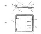
図3はこの種の従来構造を示し、図3(a)は平面図、(b)は側面図でこの外形(パッケージ)構造は所謂表面実装型TO−220として良く知られており、図中6はトランスファモールド法等により樹脂成形されたモールド部で図示しないリードフレーム上に半導体基板の一面を固着し、該固着部に連接されたリードを一方の電極端子2とし、又該半導体基板の他面に電気的に接続した内部リード等を通し、他方の電極端子3とする。そして両端子2及び3は樹脂成型後同一平面上に外部取付面が形成されており、実装基板(図示せず)への面実装を容易にしている。
【0003】
上記の従来例では実装基板上に面実装しようとすると図3(a)において端子2から端子3に跨る一辺(長さa)と他辺(長さb)を乗じた(a×b)の面積を実装基板上に要する等比較的半導体デバイスが大きい場合には基板上に占めるスペースが広く、電子機器の小型化に適さない。又これらデバイスを小型化することも考えられるがトランスファモールド法で成形しようとすると、製造工程で複雑且つ高価な設備が必要となり、生産量の少ないデバイスの場合には経済的でない。
【0004】
【発明が解決しようとする課題】
本発明は上記従来技術の問題点を鑑みてなされたもので、その目的は半導体装置の構造を工夫することにより、実装床面積が少なく小型、薄型のパワーCSPタイプの半導体装置を提供することにある。
【0005】
【課題を解決するための手段】
上記目的を達成するために本発明の半導体装置は、金属ケース2の内側に半導体基体1と他方の接続用外部端子3を組立た後、金属ケース内に絶縁樹脂を注入して構成する為、金属ケースの接続用外部端子2aと他方の外部端子3が略同一面になっていて実装基板面に接することを特徴とする。
このような金属ケースの一部に屈曲した接続用外部端子2aと他方の外部端子3を配置する事により、実装床面積は半導体基体の外周部に一定寸法を確保するのみであり、大幅に実装床面積を低減することが可能である。
又本発明の半導体装置の金属ケースは、平板からつなぎ目の生じない絞り加工で製造することを特徴とする。このように金属ケースと接続用外部端子を絞り加工で製造すれば、放熱性の良い半導体装置を容易に実現することができる。金属ケースに絶縁樹脂を注入する構造のため、トランスファモールド用のプレス、金型や切断装置等が不要となり、製造工程が簡易で高価な設備を使用せずに生産することができる。
【0006】
【発明の実施の形態】
以下、添付図面を参照して本発明に係る半導体装置の実施形態を説明する。
尚、図面の説明において同一部材には同じ符号を付し、重複する説明は省略する。
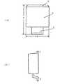
図1は本発明の第一実施形態を示しており、図1(a)は正面断面図、同図(b)は下面図である。この半導体装置は、組立用の専用治具(図示せず)を用いて、金属ケース2の内側に半導体基体1、他方の外部端子3及び接合材5を介して電気的に接続する。そして、絶縁樹脂4を金属ケース内に注入する。一方金属ケース2の一側部を予め開口部側に略平行に屈曲し、この屈曲部2aを接続用外部端子として機能せしめる。又、接続用外部端子2aと他方の外部端子3は実装時の基板面7に接する為、略同一面になっている。尚、この半導体基体1は約5mm角、金属ケース2は約6.5mm角で高さ約1.5mmにされている。他方の外部端子3は、金属ケース内に配置している。
小型・薄型化の要求に応えるために半導体基体(チップ)に略同サイズのCSPタイプの半導体装置となっている。
金属ケース2は板厚約0.3mmの平板からプレスを用いて、絞り加工により形成するためつなぎ目がなく一体であるから、半導体基体から発生する熱を効率よく放熱することができる。
【0007】
図2は本発明の他の実施例構造で,(a)は正面断面図、(b)は下面図である。図2は、半導体基体1にMOSFETを用いた例であり、他方の外部端子3が2端子3a、3bとなっている。この様に、端子数が複数となる場合は、他方の外部端子3を必要数配置することにより対応できる。
【0008】
【発明の効果】
金属ケースの一部に接続用外部端子を設け、他方の外部端子も金属ケース内に配置したことにより、実装床面積が少なく機器を小型にすることができる。金属ケースを絞り加工で製造するので半導体基体からの発熱を金属ケース及び接続要外部端子から効率的に放熱する事が出来る。
【図面の簡単な説明】
【図1】 本発明の一実施例構造図
(a) 正面断面図
(b) 下面図
【図2】 本発明の他の実施例構造図
(a) 正面断面図
(b) 下面図
【図3】 従来の構造図
(a) 正面図
(b) 側面図
【符号の簡単な説明】
1 半導体基体
2 金属ケース
2a 接続用外部端子
3 他方の外部端子
4 絶縁樹脂
5 接合材
6 モールド部
7 基板[0001]
The present invention relates to a structure of a small and thin semiconductor device that can be surface-mounted on a mounting substrate, and is a generally-known CSP (Chip Size Package or Chip Scale Package) type semiconductor device.
[0002]
FIG. 3 shows this type of conventional structure, FIG. 3 (a) is a plan view, FIG. 3 (b) is a side view, and this outer shape (package) structure is well known as a so-called surface-mount type TO-220.
[0003]
In the above conventional example, when surface mounting is attempted on the mounting substrate, in FIG. 3A, one side (length a) extending from the
[0004]
[Problems to be solved by the invention]
The present invention has been made in view of the above-described problems of the prior art, and an object of the present invention is to provide a small and thin power CSP type semiconductor device with a small mounting floor area by devising the structure of the semiconductor device. is there.
[0005]
[Means for Solving the Problems]
In order to achieve the above object, the semiconductor device of the present invention is configured by injecting an insulating resin into the metal case after assembling the
By arranging the bent connection external terminal 2a and the other
In addition, the metal case of the semiconductor device of the present invention is manufactured by a drawing process in which no joint is formed from the flat plate. If the metal case and the connecting external terminal are manufactured by drawing as described above, a semiconductor device with good heat dissipation can be easily realized. The structure in which the insulating resin is injected into the metal case eliminates the need for a transfer mold press, a die, a cutting device, and the like, and the production process is simple and production can be performed without using expensive equipment.
[0006]
DETAILED DESCRIPTION OF THE INVENTION
Embodiments of a semiconductor device according to the present invention will be described below with reference to the accompanying drawings.
In the description of the drawings, the same members are denoted by the same reference numerals, and redundant descriptions are omitted.
FIG. 1 shows a first embodiment of the present invention. FIG. 1 (a) is a front sectional view and FIG. 1 (b) is a bottom view. This semiconductor device is electrically connected to the inside of the
In order to meet the demand for miniaturization and thinning, the semiconductor substrate (chip) is a CSP type semiconductor device having substantially the same size.
Since the
[0007]
2A and 2B show another embodiment of the present invention, in which FIG. 2A is a front sectional view and FIG. 2B is a bottom view. FIG. 2 shows an example in which a MOSFET is used for the
[0008]
【The invention's effect】
By providing the connection external terminal in a part of the metal case and arranging the other external terminal in the metal case, the mounting floor area is small and the device can be made compact. Since the metal case is manufactured by drawing, the heat generated from the semiconductor substrate can be efficiently radiated from the metal case and the external terminals requiring connection.
[Brief description of the drawings]
FIG. 1 is a structural view of one embodiment of the present invention (a) Front sectional view (b) bottom view [FIG. 2] Other structural view of another embodiment of the present invention (a) Front sectional view (b) Bottom view [FIG. ] Conventional structural drawing (a) Front view (b) Side view [Brief description of symbols]
DESCRIPTION OF
Claims (1)
Translated fromJapanese前記金属ケース内の平坦な底面に一方面が電気的に接続される半導体基体と、
前記金属ケース内を埋設する絶縁樹脂と、
前記半導体基体の一方面に対向する他方面に電気的に接続されており、前記絶縁樹脂から露出する外部端子と、を備えた半導体装置において、
前記金属ケースは、当該金属ケースにおける一側部が延伸して前記凹の字状の断面形状において開口する内側で前記底面と平行になるように屈曲した接続用外部端子を前記絞り加工によって一体的に有しており、
前記絶縁樹脂から露出する前記外部端子は、前記開口の内側で屈曲して前記底面と平行であり、かつ前記接続用外部端子と離間しており、
前記接続用外部端子における基板との実装面は、前記絶縁樹脂から露出する前記外部端子における基板との実装面と同じ高さ位置であり、
前記接続用外部端子における基板との実装面に対向する面は、埋設される前記絶縁樹脂に接していることを特徴とする半導体装置。A metal case having a concave cross-sectional shape by drawing a flat plate, and having a recess in the concave cross-sectional shape as an opening;
A semiconductor substrate having one surface electrically connected to a flat bottom surface in the metal case;
An insulating resin embedded in the metal case;
In the semiconductor device comprising: an external terminal that is electrically connected to the other surface facing the one surface of the semiconductor substrate and exposed from the insulating resin;
The metal case is integrally formed by drawing the connecting external terminal that is bent so that one side portion of the metal case extends and opens in the concave cross-sectional shape so as to be parallel to the bottom surface. Have
The external terminal exposed from the insulating resin is bent inside the opening and parallel to the bottom surface, and is separated from the connection external terminal,
The mounting surface with the substrate in the external terminal for connection is at the same height position as the mounting surface with the substrate in the external terminal exposed from the insulating resin,
The semiconductor device according to claim 1, wherein a surface of the external connection terminal facing the mounting surface with the substrate is in contact with the embedded insulating resin.
Priority Applications (1)
| Application Number | Priority Date | Filing Date | Title |
|---|---|---|---|
| JP27259398AJP3867881B2 (en) | 1998-09-09 | 1998-09-09 | Semiconductor device |
Applications Claiming Priority (1)
| Application Number | Priority Date | Filing Date | Title |
|---|---|---|---|
| JP27259398AJP3867881B2 (en) | 1998-09-09 | 1998-09-09 | Semiconductor device |
Publications (2)
| Publication Number | Publication Date |
|---|---|
| JP2000091475A JP2000091475A (en) | 2000-03-31 |
| JP3867881B2true JP3867881B2 (en) | 2007-01-17 |
Family
ID=17516088
Family Applications (1)
| Application Number | Title | Priority Date | Filing Date |
|---|---|---|---|
| JP27259398AExpired - LifetimeJP3867881B2 (en) | 1998-09-09 | 1998-09-09 | Semiconductor device |
Country Status (1)
| Country | Link |
|---|---|
| JP (1) | JP3867881B2 (en) |
Families Citing this family (2)
| Publication number | Priority date | Publication date | Assignee | Title |
|---|---|---|---|---|
| US6777800B2 (en)* | 2002-09-30 | 2004-08-17 | Fairchild Semiconductor Corporation | Semiconductor die package including drain clip |
| US6841865B2 (en)* | 2002-11-22 | 2005-01-11 | International Rectifier Corporation | Semiconductor device having clips for connecting to external elements |
Family Cites Families (4)
| Publication number | Priority date | Publication date | Assignee | Title |
|---|---|---|---|---|
| JPS56107565A (en)* | 1980-01-29 | 1981-08-26 | Nec Home Electronics Ltd | Sealing structure for electronic parts |
| JPH0445651U (en)* | 1990-08-23 | 1992-04-17 | ||
| JP2952286B2 (en)* | 1991-03-27 | 1999-09-20 | 国際電気株式会社 | Bare chipless dress package |
| JPH06132424A (en)* | 1992-10-16 | 1994-05-13 | Fuji Electric Co Ltd | Switching semiconductor device |
- 1998
- 1998-09-09JPJP27259398Apatent/JP3867881B2/ennot_activeExpired - Lifetime
Also Published As
| Publication number | Publication date |
|---|---|
| JP2000091475A (en) | 2000-03-31 |
Similar Documents
| Publication | Publication Date | Title |
|---|---|---|
| KR100294719B1 (en) | Molded semiconductor device and method for manufacturing the same, lead frame | |
| US6723582B2 (en) | Method of making a semiconductor package having exposed metal strap | |
| US6703696B2 (en) | Semiconductor package | |
| US7449370B2 (en) | Production process for manufacturing such semiconductor package | |
| EP0880177B1 (en) | Semiconductor device having lead terminals bent in J-shape | |
| JP3877401B2 (en) | Manufacturing method of semiconductor device | |
| CN102272922B (en) | Semiconductor die package with clip interconnect | |
| US6114750A (en) | Surface mount TO-220 package and process for the manufacture thereof | |
| JP3169578B2 (en) | Substrate for electronic components | |
| JP3867881B2 (en) | Semiconductor device | |
| JP3730469B2 (en) | Resin-sealed semiconductor device and manufacturing method thereof | |
| JP2004165525A (en) | Semiconductor device and its manufacture | |
| JP2000150725A (en) | Semiconductor device and its manufacture | |
| KR100373149B1 (en) | Semiconductor package | |
| JPH11219969A (en) | Semiconductor device | |
| JP2519332B2 (en) | Semiconductor device | |
| JP2001203321A (en) | Resin-sealed semiconductor device | |
| WO2001009953A1 (en) | Lead frame with downset die pad | |
| JPS6236299Y2 (en) | ||
| US20200035577A1 (en) | Packaged integrated circuit | |
| JPH05136327A (en) | Semiconductor package | |
| JP4067072B2 (en) | Composite semiconductor device | |
| CN112397399A (en) | Semiconductor device and packaging method thereof | |
| JP2009206343A (en) | Lead frame, semiconductor device using the same, and manufacturing method thereof | |
| JPH118336A (en) | Semiconductor device |
Legal Events
| Date | Code | Title | Description |
|---|---|---|---|
| A621 | Written request for application examination | Free format text:JAPANESE INTERMEDIATE CODE: A621 Effective date:20041221 | |
| A977 | Report on retrieval | Free format text:JAPANESE INTERMEDIATE CODE: A971007 Effective date:20060214 | |
| A131 | Notification of reasons for refusal | Free format text:JAPANESE INTERMEDIATE CODE: A131 Effective date:20060221 | |
| A521 | Written amendment | Free format text:JAPANESE INTERMEDIATE CODE: A523 Effective date:20060316 | |
| A131 | Notification of reasons for refusal | Free format text:JAPANESE INTERMEDIATE CODE: A131 Effective date:20060823 | |
| A521 | Written amendment | Free format text:JAPANESE INTERMEDIATE CODE: A523 Effective date:20060906 | |
| TRDD | Decision of grant or rejection written | ||
| A01 | Written decision to grant a patent or to grant a registration (utility model) | Free format text:JAPANESE INTERMEDIATE CODE: A01 Effective date:20061004 | |
| A61 | First payment of annual fees (during grant procedure) | Free format text:JAPANESE INTERMEDIATE CODE: A61 Effective date:20061005 | |
| R150 | Certificate of patent or registration of utility model | Free format text:JAPANESE INTERMEDIATE CODE: R150 | |
| FPAY | Renewal fee payment (event date is renewal date of database) | Free format text:PAYMENT UNTIL: 20091020 Year of fee payment:3 | |
| FPAY | Renewal fee payment (event date is renewal date of database) | Free format text:PAYMENT UNTIL: 20101020 Year of fee payment:4 | |
| FPAY | Renewal fee payment (event date is renewal date of database) | Free format text:PAYMENT UNTIL: 20101020 Year of fee payment:4 | |
| FPAY | Renewal fee payment (event date is renewal date of database) | Free format text:PAYMENT UNTIL: 20111020 Year of fee payment:5 | |
| FPAY | Renewal fee payment (event date is renewal date of database) | Free format text:PAYMENT UNTIL: 20111020 Year of fee payment:5 | |
| FPAY | Renewal fee payment (event date is renewal date of database) | Free format text:PAYMENT UNTIL: 20121020 Year of fee payment:6 | |
| FPAY | Renewal fee payment (event date is renewal date of database) | Free format text:PAYMENT UNTIL: 20121020 Year of fee payment:6 | |
| FPAY | Renewal fee payment (event date is renewal date of database) | Free format text:PAYMENT UNTIL: 20131020 Year of fee payment:7 | |
| EXPY | Cancellation because of completion of term |