JP3865459B2 - Semiconductor device mounting equipment - Google Patents
Semiconductor device mounting equipmentDownload PDFInfo
- Publication number
- JP3865459B2 JP3865459B2JP13872397AJP13872397AJP3865459B2JP 3865459 B2JP3865459 B2JP 3865459B2JP 13872397 AJP13872397 AJP 13872397AJP 13872397 AJP13872397 AJP 13872397AJP 3865459 B2JP3865459 B2JP 3865459B2
- Authority
- JP
- Japan
- Prior art keywords
- substrate
- semiconductor element
- mark
- marks
- irradiation
- Prior art date
- Legal status (The legal status is an assumption and is not a legal conclusion. Google has not performed a legal analysis and makes no representation as to the accuracy of the status listed.)
- Expired - Fee Related
Links
Images


Landscapes
- Length Measuring Devices By Optical Means (AREA)
Description
Translated fromJapanese【0001】
【発明の属する技術分野】
本発明は、小さな半導体素子を基板上に正確に位置決めした上で取り付ける半導体素子実装装置に関し、特に位置決めを、半導体素子と基板の上面に位置決めのためのマークを設け、斜め方向からそのマークを観察した像に基づいてマークを合わせることにより行う半導体素子実装装置に関する。
【0002】
【従来の技術】
基板や他の取り付け部材に半導体素子を取り付けてモジュールを組み立てることが行われている。このような場合、半導体素子を基板や取り付け部材に対して正確に位置決めした上ではんだ付けなどにより固定する。正確な位置決めを行うため、従来は半導体素子と基板や取り付け部材の上面に位置合わせ用のマークを設け、上部から顕微鏡などで観察しながらマークを合わせていた。装置の自動化を図るため、通常は顕微鏡の観察像をTVカメラで取り込んで画像処理することによりマークを認識している。
【0003】
上記のような上面に設けたマークを合わせる場合、上面に垂直な方向から観察するのが好ましい。しかし、図1に示すような、半導体基板100に第1の半導体素子102と第2の半導体素子103を所定の位置関係で取り付ける場合で、例えば半導体素子の一辺が1mm以下である素子が小型の場合などは、位置決めする状態で素子を吸着して取り付け位置に搬送する搭載アームがこれらの半導体素子の上部の空間に存在するため、半導体素子の上面を垂直な方向から観察することはできない。そこで、このような場合には、斜めの方向から観察することにより位置決めするようにしていた。
【0004】
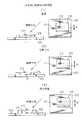
図2は、取り付ける半導体素子が小さく、斜めの方向から観察するようにした従来の半導体素子実装装置の構成を示す図である。図2に示すように、基板100は搭載ステージ1に真空吸着されて固定される。搭載ステージ1は少なくとも水平面内のX軸とY軸の2軸方向に移動可能な移動機構に取り付けられている。取り付ける半導体素子105は、搭載アーム3に真空吸着され、搭載アーム3の移動機構2により基板100上に搬送される。移動機構2は、搭載アーム3が基板100上に移動すると、搭載アーム3を降下させて半導体素子105を基板100に接触するか、接触する直前の状態まで近接させる。この状態で斜めから観察光学系の顕微鏡4で半導体素子105の部分の像をTV(CCD)カメラ5に投影する。画像処理装置6は、TVカメラ5の捕らえた半導体素子105の部分の画像を処理してモニタ8に表示すると共に、半導体素子105と基板100に設けられたマークを認識してその位置を主制御装置7に送る。主制御装置7は、送られたマークの位置から、マークが所定の位置関係、すなわち半導体素子105が基板100に対して所定の位置に配置されるようにステージ制御装置9に必要な移動量と回転量を指示する。ステージ制御装置9はこの指示された量だけ、搭載ステージ1及び搭載アームの移動機構2を回転させるように制御する。実際には、搭載ステージ1が回転するものや搭載ームの移動機構2が回転だけでなくX軸とY軸の方向に移動して位置決めを行うものなど各種の変形例がある。図1に示す光モジュールの場合には、位置決めが終了した後には、搭載ステージ1に設けられたヒータで、基板100の上面に塗られたはんだを加熱して半導体素子105を基板100に固定している。
【0005】
図3は、図2に示すような斜めからマークの像を観察する場合の画像を説明する図であり、左側が横方向からみた位置関係を、右側が観察像を示す。図3の(1)に示すように、基板100のマーク111と半導体素子105のマーク112の位置が合った時には、観察像において、基板100のマーク111と半導体素子105のマーク112の中心を通過する観察方向に垂直で素子の上面に平行な直線間の距離はaだけ離れて見える。図3の(2)に示すように、マーク111と112の位置がずれている時には、上記の距離はa’になる。従って、この距離が所定の値aになるように搭載ステージ1を移動させて、位置調整を行っている。
【0006】
【発明が解決しようとする課題】
上記のように、基板100は搭載ステージ1に保持されるが、基板100の厚さのばらつきなどのために基板100の上面の位置はばらつく。また、半導体素子105は搭載アーム3に吸着された状態で基板100に接触又は近接され、その状態でマークの位置が検出されるが、半導体素子105を基板100に接触させて停止させる場合には、半導体素子105の厚さのばらつきや基板100の上面に塗られたはんだの厚さのばらつきなどのために半導体素子105の上面の位置はばらつく。また半導体素子105を基板100に近接させて停止させる場合には、搭載アーム3の移動誤差などにより、同様に半導体素子105の上面の位置はばらつく。基板100と半導体素子105の上面の位置がばらつき、基板100と半導体素子105の上面位置の差が図3の(1)に示した状態に対して誤差を有すると、図3の(3)に示すように、たとえマーク111と112が合っていても、マーク111とマーク112の中心を通過する直線間の距離はaと異なるa''になる。すなわち、上面位置の差が増加するとマーク112がマーク111に対して左側にずれたのと同じように直線間の距離が増加し、逆に上面位置の差が減少するとマーク112がマーク111に対して右側にずれたのと同じように直線間の距離が減少する。従って、上面位置の差が予定の値と異なる場合には、直線間の距離を所定の値aになるように調整したのではマーク111と112は合っておらず、すなわち半導体素子105は基板100に対してずれており、正確な位置決めができないという問題があった。なお、上記の説明では基板の上面を水平面とした場合、水平面内の観察方向に垂直な方向の位置決めについては説明していないが、この方向の位置は基板と素子のマークのこの方向の間隔が所定の距離になるようにすることで位置決めでき、この距離は基板と素子の上面の位置の差には関係しないので、ここでは説明を省略する。
【0007】
本発明はこのような問題を解決するためのもので、半導体素子実装装置における位置決め精度を向上させることを目的とする。
【0008】
【課題を解決するための手段】
図4は、本発明の原理を説明する図であり、図5は本発明の半導体素子実装装置の原理構成図である。
図4及び図5に示すように、本発明の半導体素子実装装置では、従来の構成に加えて、観察する方向以外の方向から半導体素子と基板の上面にパターンを照射し、パターンの像を観察することにより半導体素子と基板の上面の高さの差を検出し、高さの差に応じて半導体素子と基板の上面に設けられたマークの目標とする位置関係を補正することを特徴とする。
【0009】
すなわち、本発明の半導体素子実装装置は、上面にマーク112a、112bを有する半導体素子105を、上面にマーク111a、111bを有する基板100に位置決めして取り付ける半導体素子実装装置であって、半導体素子105を基板100に対して相対的に移動させる移動機構と、基板100の上面に対して垂直以外の第1の所定角度で基板100及び半導体素子105を観察し、その観察像を出力する観察光学系4、51と、観察光学系の出力する観察像を画像処理して前記マークを認識する画像認識装置6と、画像認識装置が認識したマーク111a、111b、112a、112bが、観察像において所定の目標位置関係になるように移動機構を制御する制御装置7とを備える半導体素子実装装置において、観察光学系の観察方向以外の方向から第2の所定角度で半導体素子の上面105と基板100の上面に照射パターン121、122を照射するパターン照射系11、12、15を備え、画像認識装置6は、半導体素子105の上面と基板100の上面に照射された照射パターン121、122の相対位置を認識し、制御装置7は、認識された照射パターンの相対位置から半導体素子の上面と基板の上面の高さの差を検出して、所定の目標位置関係を補正することを特徴とする。
【0010】
パターン照射系の照射方向は、図5に示すような観察光学系の観察方向の反対側の方向であることが望ましい。
図4に示すように、基板100の上には位置決め用のマーク111aと111bが設けられており、素子105の上にも位置決め用のマーク112aと112bが設けられており、アパーチャ12のパターンを照射して基板100の上と素子105の上に2個のマーク121と122をそれぞれ照射する。この様子を横から見た図が図5である。図5に示すように、光源11からの照射光は、アパーチャ12を照射する。アパーチャ12にはマークに相当するパターンが設けられており、投影レンズ15でアパーチャ12のパターンを基板100及び素子105の表面に投影する。観察光学系を構成する投影レンズ4と撮像素子51を有する。投影レンズ4は素子105と基板100の部分の像を撮像素子51に投影し、撮像素子51は投影された観察像を画像処理装置6に送る。画像処理装置6は観察像からマークの位置を検出して主制御装置7に送る。主制御装置7には、マークの位置から素子面の基板面に対する高さを検出する素子面位置検出部71が設けられている。
【0011】
図5に示すように、素子105の上面が上方に移動した場合、マーク121の位置は変わらないが、マーク122の位置は左側の122’で示す位置に移動する。従って、マーク122の撮像素子51上の投影位置は図示のように移動する。素子105の上面が下方に移動した場合には、マーク122の撮像素子51上の投影位置は逆方向に移動する。このように、マーク122の撮像素子51上の投影位置は素子105の上面位置に応じて変化する。従って、マーク122の撮像素子51上の投影位置を検出すれば、素子105の上面位置が検出できる。位置合わせ用のマーク111と112が合っている状態で、素子105の上面位置が移動すると、マーク112の位置は図示のように112’の位置に移動し、それに応じて撮像素子51上の投影位置が変化するので、上記のように検出した素子105の上面位置に応じてマーク112が投影される撮像素子51上の位置を変化させれば、位置合わせ用のマーク111と112が合っている状態になる。実際には、基板100の上面位置も変動するので、マーク111と121の撮像素子51上の投影位置も変化する。従って、実際には、撮像素子51上のマーク121と122の投影位置の差で基板100と素子105の上面の高さの差を検出し、それに応じてマーク111と112の投影位置の差の調整目標値を変更する。
【0012】
照射パターンとして半導体素子の上面に照射される素子上マークを2個以上とし、基板の上面にも2個の基板上マークを照射し、制御装置7は、2個以上の素子上マークと2個の基板上マークの相互位置から、半導体素子の上面の基板の上面に対する傾きを検出するようにしてもよい。
本発明では、ななめから観察する場合に誤差を生じる原因となる半導体素子の上面の位置を検出して補正する。半導体素子の上面の位置の検出には触針を接触させる方式や静電容量方式など各種考えられるが、本発明では、光切断法を応用して、基板と素子の上面にマークを照射してその照射位置を位置合わせ用のマークを観察する観察光学系で観察するようにしている。これにより、観察光学系や画像処理装置をそのまま使用できるので、低コストで半導体素子の上面の位置が検出できるようになる。また、このようなパターンを照射する方式は、半導体素子の上部の空間を使用する必要がなく、装置の配置の点からも利点が多い。
【0013】
【発明の実施の形態】
図6は、本発明の第1実施例の半導体素子実装装置の全体構成を示す図である。図示のように、第1実施例の半導体素子実装装置は図2に示した従来の装置と類似の構成を有しており、高さ検出のためのパターンを照射するパターン照射系10が新たに設けられており、画像処理装置6が高さ検出のためのパターンを認識し、主制御装置7が高さ検出のためのパターンから素子面の基板面に対する高さを検出して位置合わせ用のマークの調整目標位置を変更する点が異なる。従って、異なる点についてのみ説明し、他の部分の説明は省略する。
【0014】
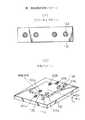
図6に示すように、パターン照射系10は、鏡筒13と光源ユニット14と顕微鏡の対物レンズ15から構成されている。図7は、パターン照射系10及び観察光学系の部分の詳細図である。
観察光学系の顕微鏡光学系4は、光軸が基板100の上面に対して45°をなすように配置されている。顕微鏡光学系4は、光源ユニット44に設けられたランプ41からの照明光をコンデンサレンズ47で効率よく鏡筒43に導くようになっている。コンデンサレンズ47を通過した照明光は、ビームスプリッタ46で基板100及び素子105に向かうように反射される。ビームスプリッタ46を通過した光は鏡筒43の表面で吸収されるようになっている。ビームスプリッタ46からの照明光は、5倍程度の対物レンズ45を介して素子105及び基板100の上に投影される。これにより素子105及び基板100の上面が照明され、観察できるようになる。これは、通常の顕微鏡の落射照明と同じである。対物レンズ45はこのようにして照明された素子105及び基板100の像をCCD素子51の面に投影する。CCD素子51は投影された素子105及び基板100の映像を画像処理装置6に出力する。以上の構成は従来のものと同じである。
【0015】
パターン照射系10は、観察光学系の反対側に、光軸が基板100の上面に対して45°をなすように配置されている。パターン照射系10では、光源ユニット14に設けられたランプ11からの照明光をコンデンサレンズ17で効率よく鏡筒13に導くようになっている。コンデンサレンズ17を通過した照明光は、ビームスプリッタ16で左上側に向かって反射される。通過した光は鏡筒の表面で吸収されるようになっている。ビームスプリッタ16で左上側に向かって反射された照明光は、アパーチャ12に入射する。アパーチャ12は、マークの部分が照明光を反射して他の部分が照明光を通過させるか、マークの部分が照明光を通過して他の部分が照明光を反射させるようになっている。アパーチャ12を通過した光は鏡筒13の上部で吸収されるので、マークの部分が照明光を反射して他の部分が照明光を通過させる場合には、明るいマークが投影され、マークの部分が照明光を通過して他の部分が照明光を反射させる場合には、暗いマークが投影されることになる。いずれを使用するかは、位置合わせ用のマークに応じて定める。対物レンズ15はアパーチャ12の像を素子105及び基板100の上に投影する。
【0016】
図8は、第1実施例におけるアパーチャ12のパターンと、照射パターンを示す図であり、(1)がアパーチャパターンを、(2)が照射パターンを示す。図示のように、基板100の上面には2個のマーク111aと111bを設け、素子105の上面には2個のマーク112aと112bを設ける。これら位置合わせ用のマークは、基板及び素子の表面が照明光をよく反射する場合には光らないマークとし、照明光を反射しにくい場合には光をよく反射するメタルなどのマークとする。図8の(1)に示すように、アパーチャ12には4個のマークが設けられており、図8の(2)に示すように、素子105の上面には2個の照射マーク122aと122bが、基板100の上面には2個の照射マーク121aと121bが照射される。
【0017】
図8の(2)に示すような位置合わせ用マーク及び照射マークから素子105を基板100に対して位置合わせする処理について説明する。図9は、素子105がX軸を中心として回転して傾いた場合の上面図と側面図である。図9の(1)に示すように、素子105の上面が基板100の上面と平行であれば、観察像におけるマーク121aと121bを結ぶ直線とマーク122aと122bを結ぶ直線は平行であり、その間の距離は素子105の上面の基板100の上面に対する高さに応じて変化する。ここで、図9の(2)に示すように、素子105の上面が基板100の上面に対してY軸を中心として回転し傾いたとすると、マーク122aと122bの素子105の上面における投影位置が変化する。従って、観察像においてもマーク122aと122bを結ぶ直線はマーク121aと121bを結ぶ直線に対して傾く。従って、マーク122aと122bを結ぶ直線のマーク121aと121bを結ぶ直線に対する傾き具合を検出すれば素子の上面の傾き具合が検出できる。
【0018】
そこで、位置調整を行う場合には、まず画像処理装置6にてパターンマッチング処理により各マークの位置を認識する。その上で、照射マーク122aと122bを結ぶ直線のマーク121aと121bを結ぶ直線に対する傾き具合を検出する。素子が基板に接触しない状態で保持されており、搭載アーム3の移動機構又は搭載ステージの回転機構により素子の基板に対する傾きが変化できるようになっている場合には、これらの直線が平行になるように、すなわち素子105が基板100に対して平行になるように調整する。相対的な傾きを調整する機構がない場合や、素子が基板の表面に接触された状態に保持されていて傾きを調整できない場合には、そのままの状態に保持して後で傾きの分を補正するため、傾き量を記憶する。ここでは傾きの調整はおこなわず、傾き量を記憶する代わりに、照射マーク122aと122bを結ぶ直線のマーク121aと121bを結ぶ直線に対する間隔を、照射マーク122aと122bの位置で検出し、あらかじめ決定されている基準となる値との差を補正値として記憶するものとする。これは、照射マーク122aと122bのX軸方向の位置は位置合わせ用マーク112aと112bの位置と同じにしており、それぞれの位置での高さとして補正すれば実質的に同じ補正が行えるためである。
【0019】
次に、素子105上の位置合わせ用マーク112aと112bの位置を補正する。この補正は、マーク112aと112bの位置に上記の補正値の1/2を乗じた値を加えることにより行う。これは図5に示すように、投影光学系とパターン照射系の光軸が垂直方向に対してα(45°)傾いているため、素子105の上面の位置の変化に対する照射マーク122aと122bの位置の変化は、マーク112aと112bの位置の2倍になるためである(投影光学系とパターン照射系の角度がそれぞれ同じなら、他の角度でも2倍になる)。このような補正を行った後の値について、マーク111aと11bを結ぶ直線とマーク112aと112bを結ぶ直線の平行具合を算出する。平行でない場合には、基板に対して素子がZ軸のまわりに回転していることを意味するので、平行になるように、搭載アーム3を回転させる。回転した後は、同様にパターンマッチングによりマークの位置を認識する。傾いている場合には、この回転により照射パターンの位置も微少量であるが変化するので、同じ処理を行って補正量を算出し、マーク112aと112bの位置を補正する。この状態で、マーク111aと11bを結ぶ直線とマーク112aと112bを結ぶ直線が所定の間隔になるように搭載ステージ1をX軸方向及びY軸方向に移動させて位置決めが完了する。その状態で搭載ステージ1に設けられたヒータを動作させて基板100に塗られたはんだを溶融させて素子105を固定する。
【0020】
第1実施例では、Y軸の回りの回転による傾きだけを問題にした。この方向の傾きは、位置合わせ用のマークの位置での素子面の高さと照射マークが照射される位置での素子面の高さの差になって現れ、照射マークで検出した素子面の高さで補正すると素子がZ軸まわりに回転している場合正確な補正が行えないという問題を生じる。第2実施例では、更にX軸の回りの回転による傾きも検出して補正を行う。
【0021】
第2実施例の半導体素子実装装置では、照射パターンが第1実施例と異なる。図10は第2実施例における照射パターンを示す図であり、(1)はアパーチャパターンを、(2)は照射パターンを示す。図10の(1)に示すように、アパーチャでは、第1実施例の1直線上に4個配列されたマークに加えて、この直線上でない上下位置に2個のマークが設けられ、図10の(2)に示すように、この2個のマークが素子105の上面にマーク122cと122dとして投影される。
【0022】
図11は、この2個のマークによるX軸のまわりの回転による傾きの検出を説明する図であり、X軸に垂直な平面内の照射マークの光路を示す図である。図示のように、素子105の上面がX軸のまわりの回転して傾くと、マーク122cと122dの素子面での投影位置が変化し、これに応じて観察方向から見たマーク122cと122dの間隔がDらdに変化する。従って、マーク122cと122dの間隔を検出すればX軸のまわりの回転による傾きが検出できる。X軸のまわりの回転による傾きにマーク122aと122bから位置合わせ用マーク112aと112bまでの距離を乗ずれば、マーク122aと122bとマーク112aと112bの間の高さの差が算出できる。従って、前述と同様の方法で算出したマーク122aと122bの位置での基準の高さとの差に、この差を加えれば位置合わせ用マーク112aと112bの基準の高さとの差が求まる。この基準の高さとの差に応じてマーク111aと111bを結ぶ直線との差を補正すれば、X軸のまわりの回転による傾きの分を補正できる。
【0023】
【発明の効果】
以上説明したように、本発明によれば、半導体素子実装装置において、位置決めを、半導体素子と基板の上面に位置決めのためのマークを設け、斜め方向からそのマークを観察し、その像に基づいて位置合せを行う場合に、より高精度に位置決めをすることが可能になる。
【図面の簡単な説明】
【図1】本発明を適用して組み立てる半導体素子と基板の例を示す図である。
【図2】従来の半導体素子実装装置の構成を示す図である。
【図3】従来例の問題点を示す図である。
【図4】本発明の原理を説明する図である。
【図5】本発明の半導体素子実装装置の原理構成図である。
【図6】本発明の第1実施例の半導体素子実装装置の全体構成を示す図である。
【図7】第1実施例の半導体素子実装装置の照明光学系の構成を示す図である。
【図8】第1実施例の照明パターンを示す図である。
【図9】第1実施例における検出量を示す図である。
【図10】本発明の第2実施例の照明パターンを示す図である。
【図11】第2実施例における光軸を含む平面内での回転成分の検出原理を説明する図である。
【符号の説明】
1…搭載ステージ
2…搭載アームの移動機構
3…搭載アーム
4…顕微鏡光学系
5…TVカメラ
6…画像処理装置
7…主制御装置
8…表示装置
9…ステージ制御装置
100…基板
102、103…半導体素子[0001]
BACKGROUND OF THE INVENTION
The present invention relates to a semiconductor element mounting apparatus that is mounted after a small semiconductor element is accurately positioned on a substrate, and in particular, positioning is provided with a mark for positioning on the upper surface of the semiconductor element and the substrate, and the mark is observed from an oblique direction. The present invention relates to a semiconductor element mounting apparatus which is performed by aligning marks based on the obtained image.
[0002]
[Prior art]
A module is assembled by attaching a semiconductor element to a substrate or other attachment member. In such a case, the semiconductor element is accurately positioned with respect to the substrate and the mounting member and then fixed by soldering or the like. In order to perform accurate positioning, conventionally, alignment marks are provided on the top surfaces of the semiconductor element and the substrate or mounting member, and the marks are aligned while observing with a microscope or the like from above. In order to automate the apparatus, the mark is usually recognized by capturing an observation image of a microscope with a TV camera and processing the image.
[0003]
When aligning the marks provided on the upper surface as described above, it is preferable to observe from a direction perpendicular to the upper surface. However, in the case where the
[0004]
FIG. 2 is a diagram showing a configuration of a conventional semiconductor element mounting apparatus in which a semiconductor element to be attached is small and is observed from an oblique direction. As shown in FIG. 2, the
[0005]
FIG. 3 is a diagram for explaining an image when the mark image is observed obliquely as shown in FIG. 2. The left side shows the positional relationship seen from the horizontal direction, and the right side shows the observation image. As shown in FIG. 3A, when the
[0006]
[Problems to be solved by the invention]
As described above, the
[0007]
The present invention is intended to solve such a problem, and an object thereof is to improve positioning accuracy in a semiconductor element mounting apparatus.
[0008]
[Means for Solving the Problems]
FIG. 4 is a diagram for explaining the principle of the present invention, and FIG. 5 is a diagram illustrating the principle of the semiconductor device mounting apparatus according to the present invention.
As shown in FIGS. 4 and 5, in the semiconductor device mounting apparatus of the present invention, in addition to the conventional configuration, the semiconductor device and the upper surface of the substrate are irradiated with a pattern from a direction other than the observation direction, and the pattern image is observed. And detecting a difference in height between the upper surface of the semiconductor element and the substrate and correcting a target positional relationship between the marks provided on the upper surface of the semiconductor element and the substrate in accordance with the difference in height. .
[0009]
That is, the semiconductor element mounting apparatus of the present invention is a semiconductor element mounting apparatus in which the
[0010]
The irradiation direction of the pattern irradiation system is preferably the direction opposite to the observation direction of the observation optical system as shown in FIG.
As shown in FIG. 4, positioning marks 111 a and 111 b are provided on the
[0011]
As shown in FIG. 5, when the upper surface of the
[0012]
As the irradiation pattern, two or more element marks are irradiated on the upper surface of the semiconductor element, and two substrate marks are also irradiated on the upper surface of the substrate. The inclination of the upper surface of the semiconductor element with respect to the upper surface of the substrate may be detected from the mutual position of the marks on the substrate.
In the present invention, the position of the upper surface of the semiconductor element that causes an error when observing from the lick is detected and corrected. Various methods such as a stylus contact method and a capacitance method can be considered for detecting the position of the upper surface of the semiconductor element. In the present invention, a light cutting method is applied to irradiate a mark on the upper surface of the substrate and the element. The irradiation position is observed with an observation optical system for observing the alignment mark. As a result, since the observation optical system and the image processing apparatus can be used as they are, the position of the upper surface of the semiconductor element can be detected at low cost. Further, the method of irradiating such a pattern does not need to use the space above the semiconductor element, and has many advantages from the standpoint of device arrangement.
[0013]
DETAILED DESCRIPTION OF THE INVENTION
FIG. 6 is a diagram showing the overall configuration of the semiconductor element mounting apparatus according to the first embodiment of the present invention. As shown in the figure, the semiconductor element mounting apparatus of the first embodiment has a configuration similar to that of the conventional apparatus shown in FIG. 2, and a
[0014]
As shown in FIG. 6, the
The microscope optical system 4 of the observation optical system is arranged so that the optical axis forms 45 ° with respect to the upper surface of the
[0015]
The
[0016]
FIG. 8 is a diagram showing the pattern of the
[0017]
A process for aligning the
[0018]
Therefore, when performing position adjustment, first, the image processing device 6 recognizes the position of each mark by pattern matching processing. Then, the degree of inclination of the straight line connecting the irradiation marks 122a and 122b with respect to the straight line connecting the
[0019]
Next, the positions of the alignment marks 112a and 112b on the
[0020]
In the first embodiment, only the inclination due to the rotation around the Y axis is a problem. The inclination in this direction appears as a difference between the height of the element surface at the position of the alignment mark and the height of the element surface at the position where the irradiation mark is irradiated, and the height of the element surface detected by the irradiation mark. If the correction is performed, there arises a problem that accurate correction cannot be performed when the element rotates around the Z axis. In the second embodiment, the inclination due to the rotation around the X axis is also detected and corrected.
[0021]
In the semiconductor element mounting apparatus of the second embodiment, the irradiation pattern is different from that of the first embodiment. FIG. 10 is a diagram showing an irradiation pattern in the second embodiment, where (1) shows an aperture pattern and (2) shows an irradiation pattern. As shown in (1) of FIG. 10, in the aperture, in addition to the four marks arranged on one straight line in the first embodiment, two marks are provided at upper and lower positions not on the straight line. As shown in (2), these two marks are projected on the upper surface of the
[0022]
FIG. 11 is a diagram for explaining detection of inclination by rotation around the X axis by the two marks, and is a diagram showing an optical path of an irradiation mark in a plane perpendicular to the X axis. As shown in the figure, when the upper surface of the
[0023]
【The invention's effect】
As described above, according to the present invention, in the semiconductor device mounting apparatus, positioning is performed by providing a positioning mark on the top surface of the semiconductor device and the substrate, observing the mark from an oblique direction, and based on the image. When performing alignment, positioning can be performed with higher accuracy.
[Brief description of the drawings]
FIG. 1 is a diagram showing an example of a semiconductor element and a substrate assembled by applying the present invention.
FIG. 2 is a diagram showing a configuration of a conventional semiconductor element mounting apparatus.
FIG. 3 is a diagram illustrating a problem of a conventional example.
FIG. 4 is a diagram illustrating the principle of the present invention.
FIG. 5 is a principle configuration diagram of a semiconductor element mounting apparatus according to the present invention.
FIG. 6 is a diagram showing an overall configuration of a semiconductor device mounting apparatus according to a first embodiment of the present invention.
FIG. 7 is a diagram showing a configuration of an illumination optical system of the semiconductor device mounting apparatus according to the first embodiment.
FIG. 8 is a diagram showing an illumination pattern of the first embodiment.
FIG. 9 is a diagram showing a detection amount in the first embodiment.
FIG. 10 is a diagram showing an illumination pattern according to the second embodiment of the present invention.
FIG. 11 is a diagram for explaining the principle of detecting a rotation component in a plane including the optical axis in the second embodiment.
[Explanation of symbols]
DESCRIPTION OF
Claims (3)
Translated fromJapanese前記半導体素子を前記基板に対して相対的に移動させる移動機構と、
前記基板の上面に対して垂直以外の第1の所定角度で前記基板及び前記半導体素子を観察し、その観察像を出力する観察光学系と、
前記観察光学系の出力する前記観察像を画像処理して前記マークを認識する画像認識装置と、
該画像認識装置が認識した前記マークが、前記観察像において所定の目標位置関係になるように前記移動機構を制御する制御装置とを備える半導体素子実装装置において、
前記観察光学系の観察方向以外の方向から第2の所定角度で前記半導体素子の上面と前記基板の上面に照射パターンを照射するパターン照射系を備え、
前記画像認識装置は、前記半導体素子の上面と前記基板の上面に照射された前記照射パターンの相対位置を認識し、
前記制御装置は、認識された前記照射パターンの相対位置から前記半導体素子の上面と前記基板の上面の高さの差を検出して、前記所定の目標位置関係を補正することを特徴とする半導体素子実装装置。A semiconductor element mounting apparatus for positioning and attaching a semiconductor element having a mark on an upper surface to a substrate having a mark on an upper surface,
A moving mechanism for moving the semiconductor element relative to the substrate;
An observation optical system for observing the substrate and the semiconductor element at a first predetermined angle other than perpendicular to the upper surface of the substrate and outputting an observation image;
An image recognition device for recognizing the mark by performing image processing on the observation image output from the observation optical system;
In a semiconductor element mounting apparatus comprising: a control device that controls the moving mechanism so that the mark recognized by the image recognition device has a predetermined target positional relationship in the observation image;
A pattern irradiation system for irradiating an irradiation pattern on the upper surface of the semiconductor element and the upper surface of the substrate at a second predetermined angle from a direction other than the observation direction of the observation optical system;
The image recognition device recognizes a relative position of the irradiation pattern irradiated on the upper surface of the semiconductor element and the upper surface of the substrate;
The control device detects a difference in height between the upper surface of the semiconductor element and the upper surface of the substrate from the recognized relative position of the irradiation pattern, and corrects the predetermined target positional relationship. Device mounting device.
前記パターン照射系の照射方向は、前記観察光学系の観察方向の反対側の方向である半導体素子実装装置。The semiconductor element mounting apparatus according to claim 1,
The semiconductor element mounting apparatus, wherein an irradiation direction of the pattern irradiation system is a direction opposite to an observation direction of the observation optical system.
前記照射パターンは、前記半導体素子の上面に照射される2個以上の素子上マークと、前記基板の上面に照射される2個の基板上マークであり、
前記制御装置は、前記2個以上の素子上マークと前記2個の基板上マークの相互位置から、前記半導体素子の上面の前記基板の上面に対する傾きを検出する半導体素子実装装置。The semiconductor element mounting apparatus according to claim 2,
The irradiation pattern is two or more element marks irradiated on the upper surface of the semiconductor element, and two substrate marks irradiated on the upper surface of the substrate,
The said control apparatus is a semiconductor element mounting apparatus which detects the inclination with respect to the upper surface of the said board | substrate with respect to the upper surface of the said board | substrate from the mutual position of the said 2 or more element mark and the said 2 board | substrate mark.
Priority Applications (1)
| Application Number | Priority Date | Filing Date | Title |
|---|---|---|---|
| JP13872397AJP3865459B2 (en) | 1997-05-28 | 1997-05-28 | Semiconductor device mounting equipment |
Applications Claiming Priority (1)
| Application Number | Priority Date | Filing Date | Title |
|---|---|---|---|
| JP13872397AJP3865459B2 (en) | 1997-05-28 | 1997-05-28 | Semiconductor device mounting equipment |
Publications (2)
| Publication Number | Publication Date |
|---|---|
| JPH10332345A JPH10332345A (en) | 1998-12-18 |
| JP3865459B2true JP3865459B2 (en) | 2007-01-10 |
Family
ID=15228651
Family Applications (1)
| Application Number | Title | Priority Date | Filing Date |
|---|---|---|---|
| JP13872397AExpired - Fee RelatedJP3865459B2 (en) | 1997-05-28 | 1997-05-28 | Semiconductor device mounting equipment |
Country Status (1)
| Country | Link |
|---|---|
| JP (1) | JP3865459B2 (en) |
Families Citing this family (4)
| Publication number | Priority date | Publication date | Assignee | Title |
|---|---|---|---|---|
| JP2000326082A (en)* | 1999-05-20 | 2000-11-28 | Sumitomo Heavy Ind Ltd | Laser beam machine |
| JP4763910B2 (en)* | 2001-04-05 | 2011-08-31 | 三菱重工業株式会社 | Moving object contact judgment method |
| US7253443B2 (en) | 2002-07-25 | 2007-08-07 | Advantest Corporation | Electronic device with integrally formed light emitting device and supporting member |
| US7193728B2 (en) | 2002-08-07 | 2007-03-20 | Advantest Corporation | Processing apparatus, processing method and position detecting device |
- 1997
- 1997-05-28JPJP13872397Apatent/JP3865459B2/ennot_activeExpired - Fee Related
Also Published As
| Publication number | Publication date |
|---|---|
| JPH10332345A (en) | 1998-12-18 |
Similar Documents
| Publication | Publication Date | Title |
|---|---|---|
| JP4883181B2 (en) | Component mounting method | |
| JPH09273910A (en) | Optical measuring apparatus | |
| JP2008070135A (en) | Optical axis deviation detection method of imaging apparatus, and component position detection method and apparatus | |
| JP3865459B2 (en) | Semiconductor device mounting equipment | |
| JP2005347412A (en) | Sucked state inspection apparatus, surface mounter, and part testing apparatus | |
| WO2022091927A1 (en) | Position displacement detection method, position displacement detection device, positioning device, and inspection device | |
| JP4901451B2 (en) | Component mounting equipment | |
| US8028427B2 (en) | Apparatus and method for positioning a workpiece | |
| JP3860919B2 (en) | Component recognition mounting apparatus and component recognition method | |
| JP2003179122A (en) | Board inspection equipment | |
| JP2022107020A (en) | Measuring device and component mounting machine | |
| JP3254704B2 (en) | Exposure apparatus and exposure method | |
| JP4334917B2 (en) | Alignment device | |
| JP2006100590A (en) | Proximity exposure equipment | |
| JP2000196300A (en) | Object recognition and placement device | |
| JP2861671B2 (en) | Overlay accuracy measuring device | |
| JP3337499B2 (en) | Printed circuit board inspection equipment | |
| JP4631497B2 (en) | Proximity exposure equipment | |
| JP3604801B2 (en) | Exposure apparatus and exposure method | |
| JP2004108957A (en) | Board inspection equipment | |
| JPH06300523A (en) | Part mounting device and its positioning method | |
| JP4729328B2 (en) | Defect correction device | |
| CN120266263A (en) | Positioning device and positioning method | |
| US20020085188A1 (en) | Apparatus and method for compensating for distortion of a printed circuit workpiece substrate | |
| JPH1026591A (en) | Apparatus and method for inspection as well as mounting apparatus |
Legal Events
| Date | Code | Title | Description |
|---|---|---|---|
| A977 | Report on retrieval | Free format text:JAPANESE INTERMEDIATE CODE: A971007 Effective date:20050328 | |
| TRDD | Decision of grant or rejection written | ||
| A01 | Written decision to grant a patent or to grant a registration (utility model) | Free format text:JAPANESE INTERMEDIATE CODE: A01 Effective date:20060905 | |
| A61 | First payment of annual fees (during grant procedure) | Free format text:JAPANESE INTERMEDIATE CODE: A61 Effective date:20061003 | |
| R150 | Certificate of patent or registration of utility model | Free format text:JAPANESE INTERMEDIATE CODE: R150 | |
| FPAY | Renewal fee payment (event date is renewal date of database) | Free format text:PAYMENT UNTIL: 20091013 Year of fee payment:3 | |
| FPAY | Renewal fee payment (event date is renewal date of database) | Free format text:PAYMENT UNTIL: 20101013 Year of fee payment:4 | |
| FPAY | Renewal fee payment (event date is renewal date of database) | Free format text:PAYMENT UNTIL: 20101013 Year of fee payment:4 | |
| FPAY | Renewal fee payment (event date is renewal date of database) | Free format text:PAYMENT UNTIL: 20111013 Year of fee payment:5 | |
| FPAY | Renewal fee payment (event date is renewal date of database) | Free format text:PAYMENT UNTIL: 20111013 Year of fee payment:5 | |
| FPAY | Renewal fee payment (event date is renewal date of database) | Free format text:PAYMENT UNTIL: 20121013 Year of fee payment:6 | |
| FPAY | Renewal fee payment (event date is renewal date of database) | Free format text:PAYMENT UNTIL: 20121013 Year of fee payment:6 | |
| FPAY | Renewal fee payment (event date is renewal date of database) | Free format text:PAYMENT UNTIL: 20131013 Year of fee payment:7 | |
| LAPS | Cancellation because of no payment of annual fees |