JP3863325B2 - Image display device - Google Patents
Image display deviceDownload PDFInfo
- Publication number
- JP3863325B2 JP3863325B2JP25769899AJP25769899AJP3863325B2JP 3863325 B2JP3863325 B2JP 3863325B2JP 25769899 AJP25769899 AJP 25769899AJP 25769899 AJP25769899 AJP 25769899AJP 3863325 B2JP3863325 B2JP 3863325B2
- Authority
- JP
- Japan
- Prior art keywords
- electrode
- transistor
- substrate
- image display
- display device
- Prior art date
- Legal status (The legal status is an assumption and is not a legal conclusion. Google has not performed a legal analysis and makes no representation as to the accuracy of the status listed.)
- Expired - Fee Related
Links
Images


Classifications
- G—PHYSICS
- G09—EDUCATION; CRYPTOGRAPHY; DISPLAY; ADVERTISING; SEALS
- G09G—ARRANGEMENTS OR CIRCUITS FOR CONTROL OF INDICATING DEVICES USING STATIC MEANS TO PRESENT VARIABLE INFORMATION
- G09G3/00—Control arrangements or circuits, of interest only in connection with visual indicators other than cathode-ray tubes
- G09G3/20—Control arrangements or circuits, of interest only in connection with visual indicators other than cathode-ray tubes for presentation of an assembly of a number of characters, e.g. a page, by composing the assembly by combination of individual elements arranged in a matrix no fixed position being assigned to or needed to be assigned to the individual characters or partial characters
- G09G3/22—Control arrangements or circuits, of interest only in connection with visual indicators other than cathode-ray tubes for presentation of an assembly of a number of characters, e.g. a page, by composing the assembly by combination of individual elements arranged in a matrix no fixed position being assigned to or needed to be assigned to the individual characters or partial characters using controlled light sources
- H—ELECTRICITY
- H01—ELECTRIC ELEMENTS
- H01J—ELECTRIC DISCHARGE TUBES OR DISCHARGE LAMPS
- H01J31/00—Cathode ray tubes; Electron beam tubes
- H01J31/08—Cathode ray tubes; Electron beam tubes having a screen on or from which an image or pattern is formed, picked up, converted, or stored
- H01J31/10—Image or pattern display tubes, i.e. having electrical input and optical output; Flying-spot tubes for scanning purposes
- H01J31/12—Image or pattern display tubes, i.e. having electrical input and optical output; Flying-spot tubes for scanning purposes with luminescent screen
- H01J31/123—Flat display tubes
- H01J31/125—Flat display tubes provided with control means permitting the electron beam to reach selected parts of the screen, e.g. digital selection
- H01J31/127—Flat display tubes provided with control means permitting the electron beam to reach selected parts of the screen, e.g. digital selection using large area or array sources, i.e. essentially a source for each pixel group
- G—PHYSICS
- G09—EDUCATION; CRYPTOGRAPHY; DISPLAY; ADVERTISING; SEALS
- G09G—ARRANGEMENTS OR CIRCUITS FOR CONTROL OF INDICATING DEVICES USING STATIC MEANS TO PRESENT VARIABLE INFORMATION
- G09G2300/00—Aspects of the constitution of display devices
- G09G2300/08—Active matrix structure, i.e. with use of active elements, inclusive of non-linear two terminal elements, in the pixels together with light emitting or modulating elements
- G—PHYSICS
- G09—EDUCATION; CRYPTOGRAPHY; DISPLAY; ADVERTISING; SEALS
- G09G—ARRANGEMENTS OR CIRCUITS FOR CONTROL OF INDICATING DEVICES USING STATIC MEANS TO PRESENT VARIABLE INFORMATION
- G09G2310/00—Command of the display device
- G09G2310/02—Addressing, scanning or driving the display screen or processing steps related thereto
- G09G2310/0243—Details of the generation of driving signals
- G09G2310/0251—Precharge or discharge of pixel before applying new pixel voltage
- G—PHYSICS
- G09—EDUCATION; CRYPTOGRAPHY; DISPLAY; ADVERTISING; SEALS
- G09G—ARRANGEMENTS OR CIRCUITS FOR CONTROL OF INDICATING DEVICES USING STATIC MEANS TO PRESENT VARIABLE INFORMATION
- G09G2310/00—Command of the display device
- G09G2310/02—Addressing, scanning or driving the display screen or processing steps related thereto
- G09G2310/0264—Details of driving circuits
- G09G2310/0275—Details of drivers for data electrodes, other than drivers for liquid crystal, plasma or OLED displays, not related to handling digital grey scale data or to communication of data to the pixels by means of a current
- G—PHYSICS
- G09—EDUCATION; CRYPTOGRAPHY; DISPLAY; ADVERTISING; SEALS
- G09G—ARRANGEMENTS OR CIRCUITS FOR CONTROL OF INDICATING DEVICES USING STATIC MEANS TO PRESENT VARIABLE INFORMATION
- G09G3/00—Control arrangements or circuits, of interest only in connection with visual indicators other than cathode-ray tubes
- G09G3/20—Control arrangements or circuits, of interest only in connection with visual indicators other than cathode-ray tubes for presentation of an assembly of a number of characters, e.g. a page, by composing the assembly by combination of individual elements arranged in a matrix no fixed position being assigned to or needed to be assigned to the individual characters or partial characters
- G09G3/2007—Display of intermediate tones
- G09G3/2014—Display of intermediate tones by modulation of the duration of a single pulse during which the logic level remains constant
Landscapes
- Engineering & Computer Science (AREA)
- Physics & Mathematics (AREA)
- Computer Hardware Design (AREA)
- General Physics & Mathematics (AREA)
- Theoretical Computer Science (AREA)
- Control Of Indicators Other Than Cathode Ray Tubes (AREA)
- Cathode-Ray Tubes And Fluorescent Screens For Display (AREA)
- Electrodes For Cathode-Ray Tubes (AREA)
- Vessels, Lead-In Wires, Accessory Apparatuses For Cathode-Ray Tubes (AREA)
- Devices For Indicating Variable Information By Combining Individual Elements (AREA)
Description
Translated fromJapanese【0001】
【発明の属する技術分野】
本発明は、画像表示装置に係わり、特に、発光素子をマトリクス状に並べ、それらの発光を制御することによって画像を表示する画像表示装置に適用して有効な技術に関する。
【0002】
【従来の技術】
互いに直交する電極群の交点を画素とし、各画素への印加電圧を調整することによって画像を表示するマトリクス型表示装置(マトリクス型ディスプレイ)には、液晶ディスプレイの他、フィールドエミッション・ディスプレイ(以下、FEDと称する。)、エレクトロルミネセンス・ディスプレイ(EL)、発光ダイオード・ディスプレイ(LED)などが知られている。
例えば、FEDは、特開平4−289644号公報に記載されているように、各画素毎に電子放出電子素子を配置し、そこからの放出電子を真空中で加速した後、蛍光体に照射し、照射した部分の蛍光体を発光させるものである。
FED用の電子放出素子の一例として、薄膜型電子源マトリクスがある。
薄膜型電子源とは、絶縁体に高電界を印加して生成するホットエレクトロンを利用する電子放出素子である。
以下、代表例として、上部電極−絶縁層−下部電極の3層構造の薄膜で構成されるMIM(Metal-Insulator-Metal)型電子源について説明する。
【0003】
図21は、薄膜型電子源の代表例であるMIM型電子源の動作原理を説明するための図である。
上部電極11と下部電極13との間に駆動電圧を印加して、トンネル絶縁層12内の電界を1〜10MV/cm以上にすると、下部電極13中のフェルミ準位近傍の電子はトンネル現象により障壁を透過し、トンネル絶縁層12、上部電極11の伝導帯へ注入されホットエレクトロンとなる。
これらのホットエレクトロンの一部は、トンネル絶縁層12中および上部電極11中で、固体との相互作用で散乱を受けエネルギーを失う。
この結果、上部電極11−真空10界面に到達した時点では、様々なエネルギーを有したホットエレクトロンがある。
これらのホットエレクトロンのうち、上部電極11の仕事関数(φ)以上のエネルギーを有するものは、真空10中に放出され、それ以外のものは上部電極11に流れ込む。
なお、MIM型薄膜電子源は、例えば、特開平9−320456号公報に記載されている。
ここで、上部電極11と下部電極13とを複数本設け、これら複数本の上部電極11と下部電極13と直交させて、薄膜型電子源をマトリクス状に形成すると任意の場所から電子線を発生させることができるので、画像表示装置の電子源として使用することができる。
即ち、各画素毎に薄膜型電子源素子を配置し、そこからの放出電子を真空中で加速した後、蛍光体に照射し、照射した部分の蛍光体を発光させることにより所望の画像を表示する画像表示装置を構成することができる。
薄膜型電子源は、放出電子ビームの直進性に優れるため高精細の表示装置を実現できる、表面汚染の影響を受けにくいので扱いやすい、などFED用電子放出素子として優れた特徴を有している。
【0004】
【発明が解決しようとする課題】
薄膜電子源マトリクスを用いた表示装置では、陰極線管(Cathode-ray tube;CRT)のようにシャドウマスクを用いず、またビーム偏向回路もないため、その消費電力はCRTよりもやや小さいかあるいは同程度である。
薄膜電子源マトリクスを用いた画像表示装置における従来の駆動方法による薄膜電子源マトリクスでの消費電力を概算する。
図22は、従来の薄膜電子源マトリクスの概略構成を示す図である。
行方向に伸びる行電極310に薄膜型電子源素子301の一方の電極(下部電極13)が結線され、列方向に伸びる列電極311に薄膜型電子源素子301の他方の電極(上部電極11)が結線されている。
なお、図22では3行×3列の場合を図示しているが、実際には表示装置を構成する画素、あるいはカラー表示装置の場合はサブ画素(sub-pixel)の個数だけ薄膜型電子源素子301が配置されている。
ここで、R2番目の行電極310に負の電圧パルス(−V1)を印加し、同時にC2番目の列電極311に正の電圧パルス(V2)を印加すると、R2の行電極310と、C2の列電極311との交点(R2、C2)にある薄膜型電子源素子301に(V1+V2)なる電圧が印加されるので、電子が放出される。
放出された電子は、加速されたあと蛍光体に照射し、蛍光体を発光させる。
このような線順次駆動では、単位時間にある画素が発光する期間(デューティ比)が、走査線、即ち、行電極310の本数Nに反比例する。即ち、画面の明るさは1/Nになってしまう。
しかし、1997 SID International Symposium Digest of Technical Papers、 pp. 123〜126(1997.5月)で示されているように、薄膜型電子源素子301と蛍光体を用いた画像表示装置では、パルス印加時に発光する輝度が十分高いため、線順次駆動でも十分な明るさが得られる。
また、印加電圧と輝度との関係も急峻な閾値特性を有するため、N=1000程度の場合でも単純マトリクス駆動で十分なコントラストが得られる。
即ち、液晶表示装置の場合と異なり、薄膜電子源を用いたディスプレイの場合、閾値特性を改善する目的や発光期間のデューティ比を増やす目的では、各画素にスイッチング素子を設ける必要はない。
【0005】
図22の構成で、駆動回路の無効消費電力を求めてみる。
無効消費電力とは、駆動する薄膜型電子源素子301の静電容量に電荷を充電・放電させるのに消費する電力であり、発光には寄与しない。
各薄膜型電子源素子301の1個あたりの静電容量をCeとし、列電極311の本数をM、行電極の本数をNとしたときに、行電極310に振幅Vrのパルスを1回印加した場合の無効電力は下記(1)式で表される。
【0006】
【数1】
M・Ce・Vr2 ・・・・・・・・・・・・・・・・・・・・ (1)
1秒間に画面を書き換える回数(フィールド周波数)をfとすると、N本の行電極全体での無効電力(Pr)は下記(2)で表される。
【0007】
【数2】
Pr=f・N・M・Ce・Vr2・・・・・・・・・・・・・ (2)
1本の列電極311にはN個の薄膜電子源素子が接続しているから、M本の列電極全体での無効電力(Pc)は、M本全ての列電極311にパルス電圧を印加する場合は下記(3)式で表される。
【0008】
【数3】
Pc=f・M・N・(N・Ce・Vc2) ・・・・・・・・・・ (3)
ここで、Vcは、列電極311に印加される電圧パルスの振幅である。
画面を1回書き換える期間(1フィールド期間)に列電極311にはN回パルスが印加されるので、PrとくらべてNが余分に乗ぜられている。
なお、M本の列電極311のうち、m本にパルス電圧を印加する場合は、前記(3)式のMをmに置き換えた形になる。
一例として、代表的な値、f=60Hz、N=480、M=1920、Ce=0.1nF、Vr=Vc=4Vを用いると、Pr=0.09[W]、Pc=42[W]となる。
この場合、薄膜電子源素子自体の消費電力は1.6[W]程度なので、全消費電力は44[W]程度となる。これは実用上問題ない消費電力である。
しかし、更に低消費電力化を図りたい場合は、データパルス印加に伴う無効電力Pcを削減することが有効であることがわかる。
【0009】
このように、CRTに対応した画像表示装置として用いる場合は、従来の技術でも消費電力の点からは問題ない。
しかしながら、薄膜電子源マトリクスを用いた表示装置の特徴は、薄型の表示装置が実現できることである。
このような薄型表示装置においては、ポータブルな表示装置としての用途があり、この場合、消費電力は一層低減することが望ましい。
また、各薄膜型電子源素子301の実効インピーダンスが小さい、即ち、比較的大きな電流が素子に流れるため、薄膜電子源マトリクスを線順次駆動で動作させる際、1本の電極に多数の素子の電流が流れるため、配線抵抗を十分小さくしないと画面全体で均一な明るさが得られない等の問題もあった。
さらに、電界放射型陰極、有機EL素子等をマトリクス状に配置した画像表示装置でも同じような問題があった。
本発明は、前記従来技術の問題点を解決するためになされたものであり、本発明の目的は、画像表示装置において、その消費電力を低減することが可能となる技術を提供することにある。
また、本発明の他の目的は、画像表示装置において、表示品質を向上させることが可能となる技術を提供することにある。
本発明の前記ならびにその他の目的と新規な特徴は、本明細書の記述及び添付図面によって明らかにする。
【0010】
【課題を解決するための手段】
初めに、本発明の動作原理について説明する。
図1は、本発明の画像表示装置の薄膜マトリクスの一例の概略成を示す図である。
従来では、行電極310と列電極311とが交差する領域の近傍に、薄膜型電子源素子301のみを接続していたが、図1に示すように、本発明では、行電極(本発明の第1の信号線)310と列電極(本発明の第2の信号線)311とが交差する領域の近傍に、トランジスタ302と薄膜型電子源素子301とを設け、画素トランジスタ302を経由して薄膜型電子源素子301の一方の電極(下部電極13)に駆動電圧を供給する。
即ち、画素トランジスタ302のゲート電極を行電極310に接続し、ソース電極を列電極311に接続し、さらに、ドレイン電極を薄膜型電子源素子301の一方の電極(下部電極)に接続する。
また、薄膜型電子源素子301の他方の電極(上部電極11)は、上部電極駆動回路45に結線する。
なお、トランジスタとして、薄膜トランジスタ(TFT;Thin-Film Transistor)を用いる場合は、ソース電極とドレイン電極は実質的には区別がないが、薄膜トランジスタ(TFT)の場合も含めて、本明細書では便宜的にソース電極、ドレイン電極と呼ぶことにする。
本明細書では、行電極310と列電極311とが交差する領域の近傍を交差領域と称し、また、以下の説明では、行電極310と列電極311とで囲まれる領域を「画素」と呼び、各画素領域に設けられるトランジスタ302を「画素トランジスタ」と呼ぶことにする。
さらに、カラー画像表示の場合は、赤、青、緑の各サブ画素(sub-pixel)の組み合わせで1画素(pixel)を形成するが、ここで定義した「画素」とはカラー画像表示の場合はサブ画素(sub-pixel)に相当する。
【0011】
R2番目の行電極310と、C2番目の列電極311との交差領域(R2、C2)の薄膜型電子源素子301は、以下のようにして動作させる。
R2番目の行電極310にパルス電圧を印加して、画素トランジスタ302を導通(ON)状態にする。
同時に、C2番目の列電極311に(V2)の電圧振幅のパルスを印加すると、交差領域(R2、C2)の薄膜型電子源素子301には(Vcom−V2−ΔV)なる電圧が印加され、電子が放出される。
ここで、Vcomは上部電極駆動回路45の出力電圧であり、ΔVは、画素トランジスタ302の抵抗(出力インピーダンス)による電圧降下量である。
R1番目およびR3番目の行電極310に接続されているドットでは、画素トランジスタ302がOFF状態なので、対応する薄膜型電子源素子301には電圧が印加されず、電子は放出しない。このように、本発明では、線順次駆動方式により画像表示を行う。
【0012】
本発明を用いた場合の駆動回路で消費される無効電力を概算する。
行電極駆動回路41の無効電力(Pr)は下記(4)式で表される。
【0013】
【数4】
Pr=f・N・M・Cgs・Vr2 ・・・・・・・・・・・・・ (4)
ここで、Vrは、行電極310に印加される電圧パルスの振幅であり、Cgsは、各ドットの画素トランジスタ302のゲート−ソース間寄生容量である。
通常Cgs=1pF程度であり、薄膜型電子源素子301の1個あたりの静電容量(Ce)の1/100〜1/1000程度なので、無効電力(Pr)も従来の1/100〜1/1000程度になる。
列電極駆動回路42の無効電力(Pc)は下記(5)で表される。
【0014】
【数5】
Pc=f・M・N・Ce・Vc2+f・M・N・(N−1)・Cdse・Vc2
・・・・・・・・・・・・・・・・・・ (5)
この(5)式で、第1項は画素トランジスタ302が導通状態にあるドットの寄与であり、第2項はそれ以外のドット、即ち、画素トランジスタ302がOFF状態にあるドットの寄与である。
ここで、Vcは、行電極311に印加される電圧パルスの振幅であり、Cdseは、画素トランジスタのドレイン−ソース間寄生容量(Cds)と、薄膜型電子源の301の1個あたりの静電容量(Ce)とを直列接続した合成容量であり、下記(6)式で表される。
【0015】
【数6】
したがって、無効電力(Pc)は、従来の方法に比べて約1/Nに低減させることができる。
このように、本発明によれば、駆動回路の無効電力(即ち、薄膜電子源マトリクスでの消費電力)を大幅に低減することができる。
また、駆動回路の負荷容量が小さくなることから、駆動回路に対する要求も緩和されるので、駆動回路の低コスト化にも寄与することができる。
【0016】
表示装置において、各画素にトランジスタを設けて各画素の動作を制御する方式、即ち、アクティブ・マトリクス方式と呼ばれる方式はいくつか提案・実施されている。
液晶表示装置においては、アクティブ・マトリクス方式が広く用いられているが、これは液晶素子の電圧に対する透過率の閾値特性が急峻でないため、単純マトリクス方式だとコントラストが低下してしまうためである。
アクティブ・マトリクス駆動により各画素に電圧が印加される期間を延ばし、換言すればデューティ比を大きくすることによりコントラストを向上させるためのものである。
これに対し、本発明は、各画素の動作モードは線順次駆動方式であり、即ち、発光のデューティ比は1/Nになっており、液晶表示装置でのアクティブ・マトリクス駆動とは本質的に異なる。
エレクトロルミネセンス型表示装置(ELディスプレイ)でのアクティブマトリクス駆動は、例えば、1999 SID International Symposium Digest of Technical Papers、 pp.438〜441(1999.5月)に述べられているように、各画素に最低限2個のトランジスタと蓄積容量を組み合わせて実現する。
これは、蓄積容量への電荷の出し入れを制御するトランジスタと、蓄積容量の電圧に応じて各画素のEL素子の発光を制御するトランジスタの2個を組み込んでいる。
これにより各画素のEL素子の発光期間、即ち、デューティ比を増大させ、高輝度を得るものである。したがって、この方式も、本発明とは本質的に異なる。
フィールドエミッション・ディスプレイ(FED)にアクティブマトリクス駆動を適用する例は、例えば、表面伝導型電子源のマトリクスの各ドットにトランジスタを形成する例が、特開平9−219164号に記されている。
この公知例では、表面伝導型電子源からの放出電流がドット毎にばらつくのを防ぐために、各画素のトランジスタの定電流特性を用いて電流量の均一化を図るものである。
【0017】
図2は、MOSトランジスタの、ゲート電圧一定条件でのドレイン電流(ID)対ドレイン−ソース間電圧(VDS)の関係を示したものである。
図2にから明らかなように、VDSがある値以上になると(即ち、飽和領域では)IDはVDSによらずほぼ一定になる。
前記公知例では、各ドットの画素トランジスタが、この飽和領域で動作するように印加電圧を設定し、画素トランジスタの定電流特性を利用して放出電流を一定にするものである。
電界放射陰極を電子源に用いたFEDについても、各ドットにトランジスタを設ける方式が提案されており、例えば、Proceedings of the 5th International Display Workshops、 pp.667〜670(1998.12月)に記載されているが、これも前記公知例と同様で、画素トランジスタを飽和領域で動作させ、その定電流特性を用いて電子放出のノイズの低減や放出電流の安定化を図っている。
これらの公知例で開示されている、画素トランジスタを飽和領域で動作させその定電流特性を用いる方式は、画素トランジスタの特性バラツキの影響が大きいという問題がある。
【0018】
以下、この点について説明する。
一般に、図2に示すMOSトランジスタの飽和領域でのドレイン電流ID(sat)は下記(7)式で表される。
【0019】
【数7】
ID(sat)=k・(VGS−VT)2・・・・・・・・・・・・・ (7)
ここで、VGSはトランジスタのゲート−ソース間電圧、VTは閾値電圧である。
kは、トランジスタを構成する半導体の移動度μnやゲート容量Cox、トランジスタの構造パラメータ(W,L)で表される量であり、下記(8)式で表される。
【0020】
【数8】
k=(1/2)μnCox(W/L) ・・・・・・・・・・・ (8)
実際のトランジスタでは、閾値電圧(VT)にバラツキが発生する。
飽和領域でのドレイン電流(ID(sat))は、(VGS−VT)の2乗に比例するので、閾値電圧(VT)のバラツキの影響が極めて大きい。
このため、画素トランジスタを飽和領域で動作させ、その定電流特性を用いる方式は、画素トランジスタの特性バラツキの影響が大きく、画素トランジスタを高い均一性をもって作らなければならないという問題点があった。
特に、画素トランジスタとして、アモルファスシリコン(以下、単に、a−Siと称する。)やポリシリコン(以下、単に、Poly−Siと称する。)などで構成した薄膜トランジスタ(TFT)を用いる場合には、画素TFTの均一性確保が困難になる。
本発明では、画素トランジスタ302の特性バラツキの影響を低減するために、画素トランジスタを非飽和領域、即ち、ソース電極とドレイン電極との間に印加される電圧により、ドレイン電流(ID)が大きく変化する領域で動作させる。
図2の、ドレイン電流(ID)対ドレイン−ソース間電圧(VDS)の特性で、非飽和領域の傾きの逆数、即ち、非飽和領域での有効抵抗値(出力インピーダンス)Rは、下記(9)式で表される。
【0021】
【数9】
前記(9)式から分かるように、非飽和領域の特性は、(VGS−VT)の−1乗にしか依存しないので、ID(sat)と比べて閾値電圧(VT)のバラツキの影響が小さい。
次に、図1に示すように、薄膜型電子源素子(MIM型電子源素子)301と画素トランジスタ302とを直列接続し、その全体に外部電圧(V0)を印加する場合を想定し、画素トランジスタ302の出力インピーダンス(R)のバラツキが、薄膜型電子源素子302に流れる電流に与える影響を見積もる。
薄膜型電子源素子301のダイオード電流(Id)−電圧特性(V)を、Id=f(V)、画素トランジスタの出力インピーダンスがR、R+ΔRの時に流れる電流をそれぞれI、I−ΔIとすると、下記(10)の関係がある。
【0023】
【数10】
したがって、画素トランジスタ302の出力インピーダンス(R+ΔR)を、薄膜型電子源素子301の(動作点での)微分抵抗reより小さくし、α≧1とすれば、前記(10)式は下記(11)のように変形できる。
【0025】
【数11】
これにより、画素トランジスタ302の特性バラツキ(ΔR)が表示画像の均一性に与える影響は更に小さくなる。言い換えると、画素トランジスタ302の特性バラツキの許容量が大きくなり製造しやすくなる。
画素トランジスタ302の特性バラツキの影響を小さくする別の方法は、画素トランジスタ302を非飽和領域で動作させ、列電極駆動回路42を定電流回路で構成することである。
この場合、画素トランジスタ302は、オン抵抗(R)のスイッチング素子として使用される。
画素トランジスタ302の有効抵抗(R)が変化しても、薄膜型電子源素子301に流れる電流は、列電極駆動回路42の定電流回路で規定されるので、一定電流が流れる。
この方式は、画素トランジスタとして、a−SiやPoly−Siなどで構成した薄膜トランジスタ(TFT)を用い、列電極駆動回路42に単結晶シリコン(Si)基板を用いた場合に特に有効である。
なぜなら、単結晶シリコン(Si)基板上に形成した場合は、トランジスタの特性バラツキを押さえることが容易だからである。
列電極駆動回路42を定電流回路にする構成は、印加電圧Vと発光強度Bとの関係B=g(V)に現れるバラツキや変動量と比べて、素子電流(I)との関係B=h(I)のバラツキが少ない場合に特に有効である。
このような例として、有機EL(有機エレクトロルミネッセンス)素子や発光ダイオード(LED)がある。
【0027】
即ち、本願において開示される発明のうち、代表的なものの概要を簡単に説明すれば、下記の通りである。
本発明は、複数個のトランジスタ素子と、前記各トランジスタ素子毎に設けられるとともに、下部電極と、絶縁層と、上部電極とをこの順番に積層した構造を有し、前記上部電極に正極性の電圧を印加した際に、前記上部電極表面から電子を放出する電子源素子と、第1の方向に設けられる第1の信号線と、前記第1方向と直交する第2の方向に設けられる第2信号線とを有する第1の基板と、枠部材と、蛍光体を有する第2の基板とを備え、前記第1の基板、前記枠部材および前記第2の基板とで囲まれる空間が真空雰囲気とされる表示素子を備える画像表示装置であって、前記各トランジスタ素子と前記各電子源素子とは、前記第1の信号線と前記第2の信号線との交差領域に設けられることを特徴とする。
また、本発明は、複数個のトランジスタ素子と、前記各トランジスタ素子毎に設けられるとともに、下部電極と、絶縁層と、上部電極とをこの順番に積層した構造を有し、前記上部電極に正極性の電圧を印加した際に、前記上部電極表面から電子を放出する電子源素子と、第1の方向に設けられる第1の信号線と、前記第1方向と直交する第2の方向に設けられる第2信号線とを有する第1の基板と、枠部材と、蛍光体を有する第2の基板とを備え、前記第1の基板、前記枠部材および前記第2の基板とで囲まれる空間が真空雰囲気とされる表示素子を備える画像表示装置であって、前記各トランジスタ素子は、前記第1の信号線と前記第2の信号線とで囲まれる領域内に設けられることを特徴とする。
また、本発明は、複数個のトランジスタ素子と、前記各トランジスタ素子毎に設けられるとともに、下部電極と、絶縁層と、上部電極とをこの順番に積層した構造を有し、前記上部電極に正極性の電圧を印加した際に、前記上部電極表面から電子を放出する電子源素子と、第1の方向に設けられる第1の信号線と、前記第1方向と直交する第2の方向に設けられる第2信号線とを有する第1の基板と、枠部材と、蛍光体を有する第2の基板とを備え、前記第1の基板、前記枠部材および前記第2の基板とで囲まれる空間が真空雰囲気とされる表示素子を備える画像表示装置であって、前記各トランジスタ素子の制御電極が、前記複数の第1の信号線の中の1つに電気的に接続され、前記各トランジスタ素子の第1の電極が、前記複数の第2の信号線の中の1つに電気的に接続され、前記各トランジスタ素子の第2の電極が、前記各トランジスタ素子毎に設けられる前記電子源素子の前記下部電極に電気的に接続されることを特徴とする。
また、本発明は、前記各トランジスタ素子の出力インピーダンスが、前記各電子源の動作領域での微分抵抗値よりも小さいことを特徴とする。
また、本発明は、前記各第1の信号線に駆動電圧を供給する第1の駆動手段と、前記各第2の信号線に駆動電圧を供給する第2の駆動手段とを備え、前記第2の駆動手段は、前記各第2の信号線に定電流を供給する定電流回路を有することを特徴とする。
【0028】
また、本発明は、複数個のトランジスタ素子と、前記各トランジスタ素子毎に設けられる複数個の電子放出素子と、第1の方向に設けられる第1の信号線と、前記第1方向と直交する第2の方向に設けられる第2の信号線とを有する第1の基板と、枠部材と、蛍光体を有する第2の基板とを備え、前記第1の基板、前記枠部材および前記第2の基板とで囲まれる空間が真空雰囲気とされる表示素子と、前記各第1の信号線に駆動電圧を供給する第1の駆動手段と、前記各第2の信号線に駆動電圧を供給する第2の駆動手段とを備える画像表示装置であって、前記各トランジスタ素子の制御電極は、前記複数の第1の信号線の中の1つに電気的に接続され、前記各トランジスタ素子の第1の電極は、前記複数の第2の信号線の中の1つに電気的に接続され、前記各トランジスタ素子の第2の電極は、前記各トランジスタ素子毎に設けられる前記複数個の電子放出素子に電気的に接続され、前記第2の駆動手段は、前記各第2の信号線に定電流を供給する定電流回路を有することを特徴とする。
【0029】
また、本発明は、複数個のトランジスタ素子と、前記各トランジスタ素子毎に設けられる電界発光素子と、第1の方向に設けられる第1の信号線と、前記第1方向と直交する第2の方向に設けられる第2の信号線とを有する第1の基板を備える表示素子と、前記各第1の信号線に駆動電圧を供給する第1の駆動手段と、前記各第2の信号線に駆動電圧を供給する第2の駆動手段とを備える画像表示装置であって、前記各トランジスタ素子の制御電極は、前記複数の第1の信号線の中1つに電気的に接続され、前記各トランジスタ素子の第1の電極は、前記複数の第2の信号線の中の1つに電気的に接続され、前記各トランジスタ素子の第2の電極は、前記各トランジスタ素子毎に設けられる前記各電界発光素子の第1の電極に電気的に接続され、前記第2の駆動手段は、前記各第2の信号線に定電流を供給する定電流回路を有することを特徴とする。
【0030】
また、本発明は、複数個のトランジスタ素子と、前記各トランジスタ素子毎に設けられる発光ダイオード素子と、第1の方向に設けられる第1の信号線と、前記第1方向と直交する第2の方向に設けられる第2の信号線とを有する第1の基板を備える表示素子と、前記各第1の信号線に駆動電圧を供給する第1の駆動手段と、前記各第2の信号線に駆動電圧を供給する第2の駆動手段とを備える画像表示装置であって、前記各トランジスタ素子の制御電極は、前記複数の第1の信号線の1つに電気的に接続され、前記各トランジスタ素子の第1の電極は、前記複数の第2の信号線の中の1つに電気的に接続され、前記各トランジスタ素子の第2の電極は、前記各トランジスタ素子毎に設けられる前記発光ダイオードの第1の電極に電気的に接続され、前記第2の駆動手段は、前記各第2の信号線に定電流を供給する定電流回路を有することを特徴とする。
また、本発明は、前記各トランジスタ素子が、薄膜トランジスタであり、当該薄膜トランジスタを非飽和領域で動作させることを特徴とする。
【0031】
【発明の実施の形態】
以下、図面を参照して本発明の実施の形態を詳細に説明する。
なお、実施の形態を説明するための全図において、同一機能を有するものは同一符号を付け、その繰り返しの説明は省略する。
[実施の形態1]
本発明の実施の形態1の画像表示装置は、電子放出電子源である薄膜型電子源マトリクスと蛍光体との組み合わせによって、各ドットの輝度変調素子を形成した表示パネル(本発明の表示素子)を用い、当該表示パネルの行電極及び列電極に駆動回路を接続して構成される。
ここで、表示パネルは、薄膜電子源マトリクスが形成された電子源板と蛍光体パターンが形成された蛍光表示板とから構成される。
まず、図3〜図6を用いて、本実施の形態における、画素トランジスタ305と薄膜電子源マトリクスが形成された電子源板の構造と製造方法について説明する。
図3は、本実施の形態の画素トランジスタ305の配置を表す平面図である。
図4は、本実施の形態の電子源板の要部断面構造を示す断面図であり、同図(a)は図3のA−B切断線に沿う断面図、同図(b)は図3のC−D切断線に沿う断面図である。
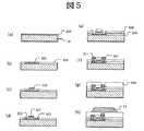
図5は、本実施の形態の画素トランジスタ302の製造方法を説明するための図であり、図6は、本実施の形態の膜型電子源マトリクスの製造方法を説明するための図である。
【0032】
以下、図5を用いて、本実施の形態の画素トランジスタ302の製造方法について説明する。
初めに、図5(a)に示すように、基板14上にジシラン(Si2H6)を原料ガスとした低圧CVD法によりa−Si膜を堆積した後、全面をレーザーアニールにして多結晶シリコン(poly−Si)膜600を形成する。
ここで、基板14には、無アルカリガラス、または二酸化シリコン(SiO2;以下、単に、SiO2と称する。)を被覆した無アルカリガラスあるいはソーダガラスを用いる。
次に、poly−Si膜600をパターン化した後、図5(b)に示すように、SiO2で構成されたゲート絶縁膜604をCVD法で形成する。
次に、図5(c)に示すように、ゲート電極601を形成した後、イオンドーピングによりpoly−Si膜600に不純物を注入し、図5(d)に示すように、ソース電極602、ドレイン電極603を形成する。
その後、図5(e)に示すように、層間絶縁膜606を形成した後、コンタクトホールを形成する。
ついで、図5(f)に示すように、列電極311と接触電極607を形成する。
続いて、図5(g)に示すように、パッシベーション膜608をSiO2で形成した後、コンタクトホールを形成する。
最後に、アルミニウム(Al;以下、単に、Alと称する。)−ネオジム(Nd;以下、単に、Ndと称する。)合金膜を形成した後、パターン化して、図5(h)に示すように、下部電極13を形成する。
ここで、下部電極13は、図3の点線で記したパターンに形成する。
【0033】
次に、図6を用いて、薄膜電子源マトリクスの一薄膜型電子源素子301の製造方法について説明する。
図6の右側の列は平面図であり、図6の左側の列は、右の図の中のA−B線に沿う断面図である。
図6(a)は、図5(h)と同一である。
まず、図6(b)に示すように、下部電極13上にレジスト501を形成する。
この状態で、陽極酸化を行い、図6(c)に示すように、保護絶縁層15を形成する。
本実施の形態では、この陽極酸化において化成電圧20V程度とし、保護絶縁層15の膜厚を30nm程度とした。
レジストパターン501をアセトンなどの有機溶媒で剥離した後、レジストで被覆されていた下部電極13表面を再度陽極酸化して、図6(d)に示すように、トンネル絶縁層12を形成する。
本実施例では、この再陽極酸化において化成電圧を6Vに設定し、絶縁層膜厚を8nmとした。
次に、上部電極バスライン用の導電膜を形成し、レジストをパターニングしてエッチングを行い、図6(e)に示すように、上部電極バスライン32を形成する。
本実施の形態では、上部電極バスライン32として、膜厚が300nm程度のAl合金と膜厚が20nm程度のタングステン(W)膜との積層膜で形成し、Al合金とタングステン(W)膜とを2段階のエッチングで加工した。
なお、上部電極バスライン32の材料には金(Au)などを用いても良い。
【0034】
また、上部電極バスライン32をエッチングする際は端部がテーパー形状になるようにエッチングした。
最後に、図6(f)に示すように、上部電極11を全面に形成する。
本実施の形態では、上部電極11として、膜厚1nmのイリジウム(Ir)、膜厚2nmの白金(Pt)、膜厚3nmの金(Au)の3層をこの順序で形成した3層積層膜を用いた。
また、上部電極11は、画像表示部分には全面に形成するが、基板周辺部の取出電極を形成した領域には形成しない。
このパターン化の精度は極めて緩いので、本実施の形態では、このパターン化を金属マスクを用いて行った。
このようにすると、上部電極形成後にレジストなどが上部電極11表面に残留することがないので、清浄な上部電極11を容易に得ることができ、電子放出特性の劣化が発生しない。
これが可能なのは、上部電極バスライン32を形成した後に上部電極11を形成しているからである。
以上のプロセスにより、基板14上に薄膜電子源マトリクスが完成する。
【0035】
本実施の形態の薄膜電子源マトリクスにおいては、トンネル絶縁層12で規定された領域(電子放出領域18、図8に記載)、即ち、レジストパターン501で規定した領域から電子が放出される。
電子放出領域18の周辺部には、厚い絶縁膜である保護絶縁層15を形成してあるため、上部電極−下部電極間に印加される電界が下部電極13の辺または角部に集中しなくなり、長時間にわたって安定な電子放出特性が得られる。
本実施の形態では、図4からわかるように、画素トランジスタ302と薄膜型電子源素子301とは、基板14上の別の層に形成している。
このため、図3からわかるように、薄膜型電子源素子301の大きさを小さくすることなく、画素トランジスタ302の大きさを大きくすることが可能である。
したがって、画素トランジスタ302の出力インピーダンスを容易に小さくすることができる。
本実施の形態では、薄膜型電子源素子301の動作領域での微分抵抗値(re)よりも、画素トランジスタ302の出力インピーダンスが小さくなるように設定した。これにより、前記したように、画素トランジスタ302の特性バラツキが表示画像の輝度ムラに影響しにくくなる。
図3の平面図から明らかなように、画素トランジスタ部は、下部電極13の下側に設けている。これにより、下部電極13が画素トランジスタ302の遮光層としても働く。
【0036】
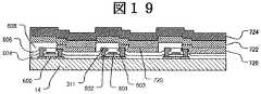
以下、図7〜図9を用いて、本実施の形態の表示パネルの構造を説明する。
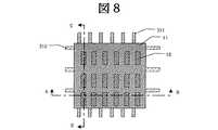
図7は、本実施の形態の表示パネルを、蛍光表示板側から見た平面図であり、図8は、本実施の形態の表示パネルから蛍光表示板を取り除き、表示パネルの蛍光表示板側から基板14を見た平面図である。
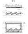
図9は、本実施の形態の表示パネルの構成を示す要部断面図であり、同図(a)は、図7、図8中のA−B切断線に沿う要部断面図、同図(b)は、図7、図8中のC−D切断線に沿う断面図である。
但し、図7、図8においては、基板14の図示は省略している。
本実施の形態の蛍光表示板は、ソーダガラス等の基板110に形成されるブラックマトリクス120と、このブラックマトリクス120の溝内に形成される赤(R)・緑(G)・青(B)の蛍光体(114A〜114C)と、これらの上に形成されるメタルバック膜122とで構成される。
以下、本実施の形態の蛍光表示板の作成方法について説明する。
まず、表示装置のコントラストを上げる目的で、基板110上に、ブラックマトリクス120を形成する(図9(a)参照)。
ブラックマトリクス120は、図7において蛍光体(114A〜114C)間に配置されるが、図7では記載を省略した。
次に、赤色蛍光体114A、緑色蛍光体114B、青色蛍光体114Cを形成する。
これら蛍光体のパターン化は、通常の陰極線管の蛍光面に用いられるのと同様に、フォトリソグラフィーを用いて行った。
蛍光体としては、例えば、赤色にY2O2S:Eu(P22−R)、緑色にZn2SiO4:Mn(P1−G1)、青色にZnS:Ag(P22−B)を用いればよい。
次いで、ニトロセルロースなどの膜でフィルミングした後、基板110全体にAlを、膜厚50〜300nm程度蒸着してメタルバック膜122とする。
その後、基板110を400℃程度に加熱してフィルミング膜やPVAなどの有機物を加熱分解する。このようにして、蛍光表示板が完成する。
【0037】
このようにして製作した電子源板と蛍光表示板とを、スペーサ60を挟み込んでフリットガラスを用いて封着する。
基板110に形成された蛍光体(114A〜114C)と、基板14との位置関係は図7に示したとおりである。
図9からわかるように、基板14を上部から平面図としてみると、全面が上部電極11に覆われている。
図8には、基板14上に形成した薄膜型電子源素子301のパターンを図7に対応させて示してある。なお、図8では、図7との位置関係を明示するために、電子放出領域18を図示してある。
電子放出領域18は、保護絶縁層15で囲まれた領域であり、実際に電子が放出される領域である。
電子放出領域18の真上に蛍光体114が位置するようにしている。
また、放出された電子ビームが多少広がることを考慮し、電子放出領域18の幅は、蛍光体114の幅より小さくしてある。
基板110−基板14との間の距離は1〜3mm程度とする。
【0038】
スペーサ60はパネル内部を真空にしたときに、大気圧の外部からの力によるパネルの破損を防ぐために挿入する。
したがって、基板14、基板110に厚さ3mmのガラスを用いて、幅4cm×長さ9cm程度以下の表示面積の表示装置を製作する場合には、基板110と基板14自体の機械強度で大気圧に耐え得るので、スペーサ60を挿入する必要はない。
スペーサ60の形状は、例えば、図7のような直方体形状とする。
ここでは、3行毎にスペーサ60の支柱を設けているが、機械強度が耐える範囲で、支柱の数(密度)を減らしてかまわない。
スペーサ60としては、ガラス製またはセラミクス製で、板状あるいは柱状の支柱を並べて配置する。
封着したパネルは、1×10~7Torr程度の真空に排気して、封止する。
表示パネル内の真空度を高真空に維持するために、封止の直前あるいは直後に、パネル内の所定の位置(図示せず)でゲッター膜の形成またはゲッター材の活性化を行う。
例えば、バリウム(Ba)を主成分とするゲッター材の場合、高周波誘導加熱によりゲッター膜を形成できる。このようにして、本実施の形態の表示パネルが完成する。
このように本実施の形態では、基板110−基板14間の距離は1〜3mm程度と大きいので、メタルバック122に印加する加速電圧を3〜6KVと高電圧にできる。
したがって、前記したように、蛍光体(114A〜114C)には陰極線管(CRT)用の蛍光体を使用できる。
【0039】
図10は、本実施の形態の表示パネルに、駆動回路を接続した状態を示す結線図である。
行電極310は行電極駆動回路41に接続され、列電極311は列電極駆動回路42に接続される。
また、全画素で共通とされる上部電極バスライン32は、上部電極駆動回路45に接続される。
ここで、各駆動回路(41,42)と、電子源板との接続は、例えば、テープキャリアパッケージを異方性導電膜で圧着したものや、各駆動回路(41,42)を構成する半導体チップを、電子源板の基板14上に直接実装するチップオングラス等によって行う。
なお、図示は省略しているが、メタルバック膜122には、加速電圧源から3〜6KV程度の加速電圧が常時印加される。
また、図10では、3行、3列しか記載していないが、実際の画像表示装置は、数100行×数1000列配列されるものであって、図11ではその一部分のみ記載していることはいうまでもない。
【0040】
図11は、図10に示す各駆動回路から出力される駆動電圧の波形の一例を示すタイミングチャートである。
ここで、n番目の行電極310をRn、m番目の列電極311をCm、n番目の行電極310と、m番目の列電極311との交点のドットを(n、m)で表すことにする。
時刻t1において、R1の行電極310に、VR1なる電圧を印加する。ここでは、VR1=15Vとした。
また、C1およびC2の列電極311には、VC2=0Vなる電圧を印加し、C3の列電極311には、VC1=10Vなる電圧を印加する。
上部電極駆動回路45の出力電圧はVU1=10Vとする。
すると、R1の行電極310にゲート電極が接続された画素トランジスタ302のゲート電圧Vgは15Vとなるので、各画素トランジスタ302が導通状態になる。
したがって、ドット(1,1)、(1,2)の上部電極11と下部電極13との間には(VU1−VC2)=10Vなる電圧が印加されるので、(VU1−VC2)を電子放出開始電圧以上に設定しておけば、この2つのドットの薄膜型電子源素子からは電子が真空10中に放出される。
放出された電子は、メタルバック膜112に印加された電圧により加速された後、蛍光体(114A〜114C)に衝突し、蛍光体(114A〜114C)を発光させる。
一方、ドット(1、3)の上部電極11と下部電極13との間の電圧は(VU1−VC1)=0Vなので電子は放出されない。
時刻t2において、R2の行電極310にVR1なる電圧を印加し、C1の列電極311にVC2なる電圧を印加すると、同様にドット(2、1)が点灯する。
このようにして、図11の電圧波形を印加すると、図10の斜線を施したドットのみが点灯する。
このようにして、列電極311に印加する信号を変えることにより所望の画像または情報を表示することができる。
また、列電極311への印加電圧の大きさをVC1〜VC2の範囲で画像信号に合わせて適宜変えることにより、階調のある画像を表示することができる。
【0041】
時刻t4において、全ての行電極301にVR1の電圧を印加して全ての画素トランジスタを導通状態にし、全ての列電極311にVC2なる電圧を印加する。
この状態で、上部電極駆動回路45の出力電圧をVU2とする。ここでは、VU2は−5V程度とした。
すると、全てのドットに対して、VU2−VC2=−5Vが印加される。
このように逆極性の電圧(反転パルス)を印加することにより薄膜型電子源素子の寿命特性を向上できる。
また、本実施の形態のように、上部電極駆動回路45に反転パルス出力機能を付けることにより、列電極駆動回路42の構成が単純になる。
回路数が多い列電極駆動回路42を単純化することは低コスト化に極めて有効である。
反転パルスを印加する期間(図10のt4〜t5、t8〜t9)としては、映像信号の垂直帰線期間を用いると、映像信号との整合性が良い。
【0042】
なお、前記説明では、画素トランジスタとしてpoly−Siを用いた薄膜トランジスタを用いた例を示したが、a−Siを用いた薄膜トランジスタ(TFT)を用いても同様の効果が得られるのは言うまでもない。
ただし、a−Siを用いたTFTを用いる場合は、基板110と基板14とを封止する際、低温封止プロセスを用いることにより、a−Siを用いたTFTの劣化を防止する必要がある。
poly−Siを用いたTFTを用いて、駆動回路(行電極駆動回路41、列電極駆動回路42または上部電極駆動回路45)を基板上に形成することもできる。この場合の基板14上の構成の一例を図12に示す。
この図12に示す構成では、基板14上に、画像表示領域101と行電極駆動回路ブロック810と列電極駆動回路ブロック811とが形成される。
画像表示領域101には、行電極310と列電極311の各交点に画素トランジスタ302と薄膜型電子源素子301を形成する。
行電極駆動回路ブロック810には、行電極310に接続する行電極駆動回路41とシフトレジスタを含む論理回路が形成される。
列電極駆動回路ブロック811には、列電極311に接続する列電極駆動回路42と直並列変換回路を含む論理回路が形成される。
このようにすると、行電極駆動回路ブロック810および列電極駆動回路ブロック811内で直列−並列変換が行われるので、基板14の外部から送る信号線の本数が大幅に削減でき、実装コストを低減できる。
【0043】
[実施の形態2]
本発明の実施の形態2の画像表示装置において、表示パネルは前記実施の形態1と同じものを用いる。
本実施の形態の画像表示装置は、列電極駆動回路42が定電流回路を有する点で、前記実施の形態1と相違する。
図13は、本実施の形態の列電極駆動回路42の一例の概略内部構成を示すブロック図である。
図13に示すように、本実施の形態の列電極駆動回路42は、定電圧回路51、定電流回路52、パルス幅変調(PWM)回路53および切替回路54を有する。
図14は、本発明の実施の形態2の画像表示装置において、各電極駆動回路(41,42,45)から出力される駆動電圧の波形の一例を示すタイミングチャートである。
なお、本実施の形態においても、図示は省略しているが、メタルバック膜122には加速電圧源から3〜6KV程度の加速電圧が常時印加される。
ここで、前記実施の形態1と同様、n番目の行電極310をRn、m番目の列電極311をCm、n番目の行電極310と、m番目の列電極311との交点のドットを(n、m)で表すことにする。
なお、図14において、駆動波形中の点線部は定電流出力を示す。
【0044】
時刻t1において、R1の行電極310への印加電圧をVR1にして、R1の行電極310にゲート電極が接続される画素トランジスタ302を導通状態にしてから、C1およびC2の列電極311に、切替回路54により定電圧回路51から定電圧VC3を短期間印加した後、切替回路54を定電流回路52に切り替え、定電流回路52により定電流出力とする。
所定の定電流パルス期間が終了後、抵抗を介して接地電位(アース電位)に接続する。なお、本実施の形態では、接地電位に接続したが、電子源の電子放出動作が停止する状態であれば他の電位であってもかまわない。
定電圧VC3は、列電極311に付帯する浮遊容量を充電するために印加するもので、定電圧印加期間は、浮遊容量を充電できる時間に設定すればよい。本実施の形態では4μsとした。
R1の行電極310にゲート電極が接続される導通状態の画素トランジスタ302により、列電極駆動回路42からの駆動電圧が印加される薄膜型電子源素子301はt1〜t2の期間電子を放出するが、この期間は本実施の形態では64μsに設定している。
したがって、電子放出量は定電流期間の放出電流でほとんど決まる。
蛍光面の発光輝度は電子放出量に比例するので、発光輝度は列電極駆動回路42の定電流出力で設定できる。
したがって、輝度−電圧特性、即ち、放出電流−電圧特性にバラツキがある場合に本方法は特に有効である。
また、定電圧印加期間の印加電圧VC3は定電流を印加した時の電圧値とほぼ等しいか、わずかに高い電圧値に設定する。なお、浮遊容量が小さく、定電流出力のみでも充分高速に追従する場合には定電圧印加期間は不要である。
同様にして、R2の行電極310以降の画素についても、列電極駆動回路の出力電流に応じて電子放出、即ち、蛍光体の発光が制御される。
結果的に、図10の斜線部の画素が発光する。
このようにして任意の画像を表示できる。
さらに、パルス幅変調(PWM)回路53により、定電流出力となる期間を制御することにより、階調のある画像を表示することができる。
あるいは、パルス幅変調の代わりに、定電流回路52の定電流出力値を階調に応じて変えて階調のある画像を表示するようにしてもよく、さらに、定電流出力値の変調とパルス幅変調を組み合わせて階調のある画像を表示するようにしてもよい。
期間(t4〜t5、t8〜t9)の反転パルス印加期間は、全ての列電極311に定電圧出力(電圧値はVC2)を印加する。
このように、本実施の形態では、各画素を薄膜型電子源素子301と画素トランジスタ302の組み合わせて構成し、かつ列電極駆動回路42に定電流回路52を用いるようにしたので、画素トランジスタ302の特性バラツキが表示画像に与える影響を低減し、表示品質を向上させることができるばかりでなく、画素トランジスタ302の特性バラツキの許容範囲を大幅に広げることができ、製造歩留まりを向上させることができる。
【0045】
[実施の形態3]
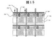
本発明の実施の形態3として、電界放射型陰極を用いた画像表示装置を、図15、図16、図17を用いて説明する。
図15は、本実施の形態における、基板上に作成される画素トランジスタと電界放射型電子源の平面図である。
図16は、本実施の形態の電界放射型陰極の要部断面構造を示す断面図であり、図15のA−B切断線の要部断面図である。
以下、図15,図16を用いて、本実施の形態の電界放射型陰極の構造について説明する。
ガラス基板14上に列電極311(画素トランジスタ302のソースを兼ねる)とクロム(Cr)等で形成した下地電極701を形成する。
オーミック・コンタクトを得るための接触層702をn+−a−Siで形成した後、a−Si:H層703を形成する。
a−Si:H層703上に、クロム(Cr)層704を介してエミッタ・チップ707をa−Siで形成する。
さらに、SiO2膜により絶縁層705を形成し、最後に、画素トランジスタ・ゲート601(行電極310と一体形成)と電界放射ゲート706とを形成する。
図16の平面図では、電界放射ゲート706のパターンは点線で記してある。
電界放射ゲート706は電子源マトリクス内の全画素に対して共通とする。
したがって、この電子源マトリクスの構成は図1において薄膜型電子源素子301の部分に代わりに電界放射型電子源を配置したものに等しい。
なお、この実施の形態の構造は、例えば、International Display Workshop'98 Proceedings、 pp.667-670(1998)に記された製法で製造できる。
この基板を、図7〜図9と同様に、電子源素子と蛍光体とを位置を合わせてパネル封止し、表示パネルとする。
このパネルは、図1に示したように駆動回路に結線する。
ただし、図1において、301を電界放射型電子源と読み換え、32、45をそれぞれ電界放射ゲート706、電界放射ゲート駆動回路45と読み替える。
【0046】
図17は、本実施の形態3の画像表示装置において、各駆動回路から出力される駆動電圧の波形の一例を示すタイミングチャートである。
ここで、前記実施の形態1と同様、n番目の行電極310をRn、m番目の列電極311をCmで表すことにする。
電界放射ゲート706には常時VU1=100V程度の電圧が印加されている。
したがって、電流を制限している画素トランジスタ302が導通状態になると、電界放射によりエミッタ・チップ707から真空中に電子が放出され、蛍光体を励起・発光させる。
時刻t1において、R1の行電極310に、VR1=60V程度の電圧が印加されると、R1の行電極310にゲート電極が接続された画素トランジスタ302が導通状態になる。
ここで、列電極駆動回路42から定電圧VC2を4μs程度出力した後、定電流回路に切り替える。
期間t1〜t2は64μs程度なので、期間t1〜t2に放出される電荷量は定電流設定値でほぼ支配される。
電界放射型電子源からの放出電流にはノイズが発生したり、画素により放出電流量がばらついたりするが、放出電流量は列電極駆動回路内の定電流回路により制限されるので放出電流は安定になる。
また、本実施の形態においては、画素トランジスタ302は有限な抵抗値を持つスイッチとして働いているが、定電流回路で駆動しているので、画素トランジスタ302の抵抗値のバラツキは放出電流量に影響しない。
したがって、画素トランジスタの特性バラツキが表示画像に与える影響を低減し、表示品質を向上させることができるばかりでなく、画素トランジスタの特性バラツキの許容範囲を大幅に広げることができ、製造歩留まりを向上させることができる。
なお、定電流出力に先立って短期間定電圧出力をするのは、列電極311に伴う浮遊容量を高速に充電するためである。したがって、定電流出力のみで高速に応答する場合はこの定電圧出力は不要である。
同様にして、R2の行電極310以降の画素についても、列電極駆動回路の出力電流に応じて電子放出、即ち、蛍光体の発光が制御される。
結果的に、図10の斜線部の画素が発光する。
このようにして任意の画像を表示できる。
本実施の形態は、電界放射型電子源を用いた場合を記したが、本実施の形態において、表面伝導型電子源を用いても同じ効果、即ち、特性バラツキがある画素トランジスタを用いても均一な画像が得られることは明らかである。
表面伝導型電子源の作成方法は、例えば、ジャーナル・オブ・ソサイアティ・フォー・インフォメーション・ディスプレイ誌(Journal of the Society for Information Display)第5巻第4号(1997年発行)第345頁〜第348頁に記載されている。
【0047】
[実施の形態4]
本発明の実施の形態4として、有機電界発光素子(有機EL素子)を用いた画像表示装置を、図18、図19、図20を用いて説明する。
図18は、本実施の形態の画像表示装置の平面図であり、図19は、本実施の形態の画像表示装置の要部断面構造を示す断面図であり、図18のA−B切断線の要部断面図である。
以下、図18、図19を用いて、本実施の形態の画像表示装置の構造について説明する。
無アルカリガラスなどの透光性基板14の上に、ソース電極602、ドレイン電極603、poly−Si膜600、ゲート絶縁膜604、ゲート電極601で形成される薄膜トランジスタを形成する。
ゲート電極601は行電極310に結線され、ソース電極602は列電極311に結線されている。
行電極310と列電極311は層間絶縁膜606により互いに絶縁されている。
この薄膜トランジスタはパッシベーション膜608で被覆されている。
パッシベーション膜608は、図18中に点線で示すパターンから分かるように、行電極310と列電極311をも被覆する。
これらの構造は、前記実施の形態1と同様の方法で形成できる。
ドレイン電極603は、接続電極607を介して陽極720に接続される。
陽極720は、例えば、ITO膜(Snをドープした酸化インジウム膜)など透明な電極を用いる。
陽極720上には、有機発光層722が全面に形成される。
有機発光層722は、陽極側からホール注入層、ホール輸送層、有機発光層、電子輸送層の順に積層したものであり、それぞれの材料組成は、例えば、1997 SID International Symposium Digest of Technical Papers、1073頁〜1076頁(1997年5月発行)に記載されている。
あるいは、有機発光層722として、1999 SID International Symposium Digest of Technical Papers、 pp.372〜375(1999.5月)に記されたポリマー型の発光層を用いても良い。
また、有機発光層722上には、陰極724が全面に形成される。
図18、図19には示していないが、最後にマトリクス全体を保護膜で被覆し、水分などの侵入を防ぐ。
このように、各画素の有機EL素子の陽極720が画素トランジスタのドレイン電極に接続され、陰極724が全画素共通電極となっている。
したがって、マトリクスとしての回路構成は、図1において、301を有機EL素子と読み替え、32を陰極724、45を陰極駆動回路と読み替えた構成になる。
【0048】
図20は、本実施の形態4の画像表示装置において、各駆動回路から出力される駆動電圧の波形の一例を示すタイミングチャートである。
ここで、前記実施の形態1と同様、n番目の行電極310をRn、m番目の列電極311をCmで表すことにする。
陰極724には、常時一定電圧VU1を印加する。本実施の形態ではVU1=0Vとした。
時刻t1において、R1の行電極311に、VR1=15V程度の電圧を印加すると、R1の行電極311にゲート電極が接続された画素トランジスタ302が導通状態になる。
ここで、列電極駆動回路から定電圧VC3(ただし、VC3>VU1)を4μs程度出力した後、定電流回路に切り替える。
すると、有機EL素子の陽極720から陰極724に向かって電流が流れ、有機発光層722が発光する。
期間t1〜t2は64μs程度なので、期間t1〜t2に有機EL素子に流れる電荷量は定電流設定値でほぼ支配される。
有機EL素子の電圧−輝度特性には画素によりバラツキがある場合があるが、注入電流量は列電極駆動回路内の定電流回路により制限されるので一定になり、発光輝度も定電流回路の設定値により規定され、バラツキが解消される。
また、本実施の形態においては、画素トランジスタ302は有限な抵抗値を持つスイッチとして働いているが、定電流回路で駆動しているので、画素トランジスタ302の抵抗値のバラツキは放出電流量に影響しない。
なお、定電流出力に先立って短期間定電圧出力をするのは、列電極311に伴う浮遊容量を高速に充電するためである。したがって、定電流出力のみで高速に応答する場合はこの定電圧出力は不要である。
同様にして、R2の行電極311以降の画素についても列電極駆動回路の出力電流に応じて有機EL素子の発光が制御される。
結果的に、図10の斜線部の画素が発光する。このようにして任意の画像を表示できる。
【0049】
本実施の形態で述べたように、有機EL素子を画素トランジスタ302とを用いて画像表示装置を構成すると、従来の画素トランジスタを用いないものと比べて、以下の利点がある。
従来の方式では、選択した行電極310には、その行電極310の接続された全ての有機EL素子の電流が流れるので、配線抵抗を十分に低くしなければならないが、本実施の形態では行電極310に電流が集中しないので配線抵抗の制約が緩和される。
即ち、従来の方式で行電極に集中して流れていた電流は、本実施の形態では陰極724に流れるが、陰極724は全面に形成されたベタ電極なので、電流が分散して流れる。
また、本実施の形態では陰極724は全画素共通なので陰極のパターン化が不要であり、製造が容易である。
また、すでに述べたように、本実施の形態では有機EL素子の電流−電圧特性にバラツキがあっても許容される。
さらに、画素トランジスタの特性バラツキが表示画像に与える影響を低減し、表示品質を向上させることができるばかりでなく、画素トランジスタの特性バラツキの許容範囲を大幅に広げることができ、製造歩留まりを向上させることができる。
一方、定電流回路を構成した画素トランジスタと有機EL素子を組み合わせた画像表示装置が、例えば、1999 SID International Symposium Digest of Technical Papers、 pp. 438〜441 (1999. 5月)に記されている。
この文献記載の方式では、1画素に4個のトランジスタが必要だが、本発明では1個で済み、作りやすい。
また、各画素2個のトランジスタの構成で定電流回路を方法も提案されているが、この場合は画素トランジスタの飽和領域の定電流特性を利用するため、前述のように画素トランジスタのバラツキの影響が大きく、製造が困難である。
なお、有機EL素子の代わりに発光ダイオードを用いて図1の構成にした場合も、本実施の形態と同様の効果を得られることはいうまでもない。
以上、本発明者によってなされた発明を、前記実施の形態に基づき具体的に説明したが、本発明は、前記実施の形態に限定されるものではなく、その要旨を逸脱しない範囲において種々変更可能であることは勿論である。
【0050】
【発明の効果】
本願において開示される発明のうち代表的なものによって得られる効果を簡単に説明すれば、下記の通りである。
(1)本発明によれば、画像表示装置の消費電力を低減することができる。
(2)本発明によれば、表示画像の輝度ばらつきを低減し、表示品質を向上させることが可能となる。
【図面の簡単な説明】
【図1】本発明の画像表示装置の薄膜マトリクスの一例の概略成を示す図である。
【図2】MOSトランジスタの特性を説明するための図である。
【図3】本発明の実施の形態1の画素トランジスタの配置を表す平面図である。
【図4】本発明の実施の形態1の電子源板の要部断面構造を示す断面図である。
【図5】本発明の実施の形態1の画素トランジスタの製造方法を説明するための図である。
【図6】本発明の実施の形態1の膜型電子源マトリクスの製造方法を説明するための図である。
【図7】本発明の実施の形態1の表示パネルを、蛍光表示板側から見た平面図である。
【図8】本発明の実施の形態1の表示パネルから蛍光表示板を取り除き、表示パネルの蛍光表示板側から電子源板を見た平面図である。
【図9】本発明の実施の形態1の表示パネルの構成を示す要部断面図である。
【図10】本発明の実施の形態1の表示パネルに、駆動回路を接続した状態を示す結線図である。
【図11】図10に示す各駆動回路から出力される駆動電圧の波形の一例を示すタイミングチャートである。
【図12】本発明の実施の形態1の表示パネルにおいて、各駆動回路を電子源板上に形成した例を示すブロック図である。
【図13】本発明の実施の形態2の列電極駆動回路の一例の概略内部構成を示すブロック図である。
【図14】本発明の実施の形態2の画像表示装置において、各電極駆動回路から出力される駆動電圧の波形の一例を示すタイミングチャートである。
【図15】本発明の実施の形態3の画像表示装置における、基板上に作成される画素トランジスタと電界放射型電子源の平面図である。
【図16】本発明の実施の形態3の電界放射型陰極の要部断面構造を示す断面図である。
【図17】本発明の実施の形態3の画像表示装置において、各駆動回路から出力される駆動電圧の波形の一例を示すタイミングチャートである。
【図18】本発明の実施の形態4の画像表示装置の平面図である。
【図19】本発明の実施の形態4の画像表示装置の要部断面構造を示す断面図である。
【図20】本発明の実施の形態4の画像表示装置において、各駆動回路から出力される駆動電圧の波形の一例を示すタイミングチャートである。
【図21】薄膜型電子源の代表例であるMIM型電子源の動作原理を説明するための図である。
【図22】従来の薄膜電子源マトリクスの概略構成を示す図である。
【符号の説明】
10…真空、11…上部電極、12…トンネル絶縁層、13…下部電極、14,110…基板、15…保護層、32…上部電極バスライン、41…行電極駆動回路、42…列電極駆動回路、45…上部電極駆動回路、51…低電圧回路、52…定電圧回路、53…パルス幅変調回路、60…スペーサ、54…切替回路、114A…赤色蛍光体、114B…緑色蛍光体、114C…青色蛍光体、120…ブラックマトリクス、122…メタルバック膜、301…薄膜型電子源素子、302…画素トランジスタ、310…行電極、311…列電極、501…レジスト、600…多結晶シリコン(Si)膜、601…ゲート電極、602…ソース電極、603…ドレイン電極、604…ゲート絶縁膜、606…層間絶縁膜、607…接触電極、608…パッシベーション膜、701…下地電極、702…接触層、703…a−Si:H膜、704…クロム(Cr)層、705…絶縁膜、706…電界放射ゲート、707…エミッタ・チップ、720…陽極、722…有機発光層、724…陰極、810…行電極駆動回路ブロック、811…列電極駆動回路ブロック。[0001]
BACKGROUND OF THE INVENTION
The present invention relates to an image display device, and more particularly to a technique effective when applied to an image display device that displays an image by arranging light emitting elements in a matrix and controlling the light emission.
[0002]
[Prior art]
A matrix type display device (matrix type display) that displays an image by adjusting an applied voltage to each pixel as an intersection of electrode groups orthogonal to each other includes a field emission display (hereinafter, referred to as a field emission display). Known as FED), electroluminescent display (EL), light emitting diode display (LED), and the like.
For example, as described in Japanese Patent Application Laid-Open No. 4-289644, the FED arranges an electron-emitting electron element for each pixel, accelerates the emitted electrons from the pixel in a vacuum, and then irradiates the phosphor. The phosphor in the irradiated part emits light.
An example of an electron emission element for FED is a thin film type electron source matrix.
A thin-film electron source is an electron-emitting device that uses hot electrons generated by applying a high electric field to an insulator.
Hereinafter, as a representative example, an MIM (Metal-Insulator-Metal) type electron source constituted by a thin film having a three-layer structure of an upper electrode, an insulating layer, and a lower electrode will be described.
[0003]
FIG. 21 is a diagram for explaining the operating principle of an MIM type electron source that is a typical example of a thin film type electron source.
When a driving voltage is applied between the
Some of these hot electrons are scattered by the interaction with the solid in the
As a result, when reaching the interface between the
Among these hot electrons, those having an energy equal to or higher than the work function (φ) of the
The MIM type thin film electron source is described in, for example, Japanese Patent Application Laid-Open No. 9-320456.
Here, when a plurality of
In other words, a thin-film electron source element is arranged for each pixel, and the emitted electrons are accelerated in a vacuum, and then irradiated onto the phosphor, and a desired image is displayed by emitting the phosphor at the irradiated portion. An image display device can be configured.
The thin-film electron source has excellent characteristics as an electron-emitting device for FED, such as being able to realize a high-definition display device because it is excellent in straightness of the emitted electron beam, and being easy to handle because it is hardly affected by surface contamination. .
[0004]
[Problems to be solved by the invention]
A display device using a thin-film electron source matrix does not use a shadow mask and does not have a beam deflection circuit as in a cathode-ray tube (CRT), so that its power consumption is slightly smaller than or equal to that of a CRT. Degree.
The power consumption in the thin film electron source matrix by the conventional driving method in the image display device using the thin film electron source matrix is estimated.
FIG. 22 is a diagram showing a schematic configuration of a conventional thin film electron source matrix.
One electrode (lower electrode 13) of the thin film
Note that FIG. 22 shows a case of 3 rows × 3 columns, but in actuality, the thin film electron source is the same as the number of pixels constituting the display device or the number of sub-pixels in the case of a color display device. An
Here, when a negative voltage pulse (−V1) is applied to the R2
The emitted electrons are accelerated and then irradiated onto the phosphor, causing the phosphor to emit light.
In such line-sequential driving, a period (duty ratio) in which a pixel in a unit time emits light is inversely proportional to the number N of scanning lines, that is,
However, as shown in 1997 SID International Symposium Digest of Technical Papers, pp. 123-126 (May 1997.5), the image display device using the thin film
In addition, since the relationship between the applied voltage and the luminance has a steep threshold characteristic, even when N = 1000, sufficient contrast can be obtained by simple matrix driving.
That is, unlike a liquid crystal display device, in the case of a display using a thin film electron source, it is not necessary to provide a switching element in each pixel for the purpose of improving threshold characteristics and increasing the duty ratio of the light emission period.
[0005]
The reactive power consumption of the drive circuit is obtained with the configuration of FIG.
The reactive power consumption is power consumed to charge / discharge electric charges in the capacitance of the driven thin film
Applying a pulse of amplitude Vr to the
[0006]
[Expression 1]
M ・ Ce ・ Vr2 (1)
When the number of times the screen is rewritten per second (field frequency) is f, the reactive power (Pr) in the entire N row electrodes is expressed by the following (2).
[0007]
[Expression 2]
Pr = f, N, M, Ce, Vr2 (2)
Since N thin-film electron source elements are connected to one
[0008]
[Equation 3]
Pc = f · M · N · (N · Ce · Vc2 ) (3)
Here, Vc is the amplitude of the voltage pulse applied to the
Since a pulse is applied N times to the
Note that, when a pulse voltage is applied to m of the
As an example, using typical values, f = 60 Hz, N = 480, M = 1920, Ce = 0.1 nF, Vr = Vc = 4 V, Pr = 0.09 [W], Pc = 42 [W] It becomes.
In this case, since the power consumption of the thin film electron source element itself is about 1.6 [W], the total power consumption is about 44 [W]. This is power consumption that is not problematic in practice.
However, it can be seen that it is effective to reduce the reactive power Pc accompanying the data pulse application in order to further reduce the power consumption.
[0009]
Thus, when used as an image display device compatible with CRT, there is no problem in terms of power consumption even with the conventional technology.
However, a feature of a display device using a thin film electron source matrix is that a thin display device can be realized.
Such a thin display device has an application as a portable display device. In this case, it is desirable to further reduce power consumption.
Also, since the effective impedance of each thin film
Further, the image display apparatus in which field emission cathodes, organic EL elements and the like are arranged in a matrix has the same problem.
The present invention has been made to solve the above-described problems of the prior art, and an object of the present invention is to provide a technique capable of reducing power consumption in an image display device. .
Another object of the present invention is to provide a technique capable of improving display quality in an image display device.
The above and other objects and novel features of the present invention will become apparent from the description of the present specification and the accompanying drawings.
[0010]
[Means for Solving the Problems]
First, the operation principle of the present invention will be described.
FIG. 1 is a diagram showing an outline of an example of a thin film matrix of the image display device of the present invention.
Conventionally, only the thin-film
That is, the gate electrode of the
The other electrode (upper electrode 11) of the thin film
Note that in the case where a thin film transistor (TFT) is used as the transistor, the source electrode and the drain electrode are not substantially distinguished from each other, but the present specification includes the case of the thin film transistor (TFT). These are referred to as a source electrode and a drain electrode.
In this specification, the vicinity of the region where the
Furthermore, in the case of color image display, one pixel is formed by a combination of red, blue, and green sub-pixels. The “pixel” defined here is a color image display. Corresponds to a sub-pixel.
[0011]
The thin-film
A pulse voltage is applied to the
At the same time, when a pulse having a voltage amplitude of (V2) is applied to the
Here, Vcom is the output voltage of the upper
At the dots connected to the R1 th and R3
[0012]
The reactive power consumed by the drive circuit when the present invention is used is roughly estimated.
The reactive power (Pr) of the row
[0013]
[Expression 4]
Pr = f, N, M, Cgs, Vr2 (4)
Here, Vr is the amplitude of the voltage pulse applied to the
Usually, Cgs is about 1 pF, and the electrostatic capacity (Ce) per thin film
The reactive power (Pc) of the column
[0014]
[Equation 5]
Pc = f · M · N · Ce · Vc2 + f · M · N · (N−1) · Cdse · Vc2
(5)
In this equation (5), the first term is the contribution of dots in which the
Here, Vc is the amplitude of the voltage pulse applied to the
[0015]
[Formula 6]
Therefore, the reactive power (Pc) can be reduced to about 1 / N compared with the conventional method.
Thus, according to the present invention, the reactive power of the drive circuit (that is, the power consumption in the thin film electron source matrix) can be greatly reduced.
Further, since the load capacity of the drive circuit is reduced, the demand for the drive circuit is eased, which can contribute to cost reduction of the drive circuit.
[0016]
In a display device, several methods for controlling the operation of each pixel by providing a transistor in each pixel, that is, a method called an active matrix method have been proposed and implemented.
In the liquid crystal display device, the active matrix method is widely used. This is because the threshold characteristic of the transmittance with respect to the voltage of the liquid crystal element is not steep, and the contrast is lowered in the simple matrix method.
This is to improve the contrast by extending the period in which a voltage is applied to each pixel by active matrix driving, in other words, by increasing the duty ratio.
In contrast, according to the present invention, the operation mode of each pixel is a line-sequential driving method, that is, the duty ratio of light emission is 1 / N, which is essentially the active matrix driving in the liquid crystal display device. Different.
Active matrix driving in an electroluminescent display device (EL display) is performed at least for each pixel as described in, for example, 1999 SID International Symposium Digest of Technical Papers, pp. 438-441 (May 1999.5). This is realized by combining two transistors and a storage capacitor.
This incorporates two transistors: a transistor that controls the input and output of charges to and from the storage capacitor, and a transistor that controls the light emission of the EL element of each pixel in accordance with the voltage of the storage capacitor.
Thereby, the light emission period of the EL element of each pixel, that is, the duty ratio is increased, and high luminance is obtained. Therefore, this method is also essentially different from the present invention.
As an example of applying active matrix driving to a field emission display (FED), for example, an example in which a transistor is formed in each dot of a matrix of a surface conduction electron source is described in JP-A-9-219164.
In this known example, in order to prevent the emission current from the surface conduction electron source from varying from dot to dot, the current amount is made uniform by using the constant current characteristic of the transistor of each pixel.
[0017]
FIG. 2 shows the relationship between the drain current (ID ) and the drain-source voltage (VDS ) of the MOS transistor under a constant gate voltage condition.
As apparent from FIG. 2, when VDS exceeds a certain value (that is, in the saturation region), ID becomes substantially constant regardless of VDS .
In the known example, the applied voltage is set so that the pixel transistor of each dot operates in this saturation region, and the emission current is made constant by utilizing the constant current characteristic of the pixel transistor.
A method of providing a transistor for each dot has also been proposed for FEDs using a field emission cathode as an electron source, as described in, for example, Proceedings of the 5th International Display Workshops, pp. 667-670 (December 1998). However, this is also the same as the known example, and the pixel transistor is operated in the saturation region, and the constant current characteristic is used to reduce the noise of electron emission and stabilize the emission current.
The methods disclosed in these known examples that operate the pixel transistor in the saturation region and use the constant current characteristic have a problem that the influence of the characteristic variation of the pixel transistor is large.
[0018]
Hereinafter, this point will be described.
In general, the drain current ID (sat) in the saturation region of the MOS transistor shown in FIG. 2 is expressed by the following equation (7).
[0019]
[Expression 7]
ID (sat) = k · (VGS −VT )2 (7)
Here, VGS is a gate-source voltage of the transistor, and VT is a threshold voltage.
k is an amount represented by the mobility μn of the semiconductor constituting the transistor, the gate capacitance Cox , and the structure parameters (W, L) of the transistor, and is represented by the following equation (8).
[0020]
[Equation 8]
k = (1/2) μn Cox (W / L) (8)
In an actual transistor, the threshold voltage (VT ) varies.
Since the drain current (ID (sat)) in the saturation region is proportional to the square of (VGS −VT ), the influence of variations in the threshold voltage (VT ) is extremely large.
For this reason, the method of operating the pixel transistor in the saturation region and using the constant current characteristic has a problem that the influence of the characteristic variation of the pixel transistor is large, and the pixel transistor has to be manufactured with high uniformity.
In particular, when a thin film transistor (TFT) composed of amorphous silicon (hereinafter simply referred to as a-Si) or polysilicon (hereinafter simply referred to as Poly-Si) is used as the pixel transistor, the pixel transistor It becomes difficult to ensure the uniformity of the TFT.
In the present invention, in order to reduce the influence of the characteristic variation of the
In the characteristics of drain current (ID ) vs. drain-source voltage (VDS ) in FIG. 2, the reciprocal of the slope of the non-saturation region, that is, the effective resistance value (output impedance) R in the non-saturation region is It is expressed by equation (9).
[0021]
[Equation 9]
As can be seen from the equation (9), the characteristic of the non-saturation region depends only on the negative power of (VGS −VT ), and thus the variation of the threshold voltage (VT ) compared to ID (sat). The influence of is small.
Next, as shown in FIG. 1, it is assumed that a thin film type electron source element (MIM type electron source element) 301 and a
Assuming that the diode current (Id) -voltage characteristic (V) of the thin-film
[0023]
[Expression 10]
Therefore, when the output impedance (R + ΔR) of the
[0025]
[Expression 11]
As a result, the influence of the characteristic variation (ΔR) of the
Another method for reducing the influence of the characteristic variation of the
In this case, the
Even if the effective resistance (R) of the
This method is particularly effective when a thin film transistor (TFT) composed of a-Si, Poly-Si, or the like is used as the pixel transistor and a single crystal silicon (Si) substrate is used for the column
This is because when formed on a single crystal silicon (Si) substrate, it is easy to suppress variation in transistor characteristics.
In the configuration in which the column
Examples thereof include an organic EL (organic electroluminescence) element and a light emitting diode (LED).
[0027]
That is, the outline of a representative one of the inventions disclosed in the present application will be briefly described as follows.
The present invention has a structure in which a plurality of transistor elements are provided for each of the transistor elements, and a lower electrode, an insulating layer, and an upper electrode are stacked in this order. When a voltage is applied, an electron source element that emits electrons from the surface of the upper electrode, a first signal line provided in a first direction, and a second direction provided in a second direction orthogonal to the first direction A space including a first substrate having two signal lines, a frame member, and a second substrate having a phosphor, and surrounded by the first substrate, the frame member, and the second substrate is vacuum. An image display device including a display element that is an atmosphere, wherein each of the transistor elements and each of the electron source elements is provided in an intersection region between the first signal line and the second signal line. Features.
In addition, the present invention has a structure in which a plurality of transistor elements are provided for each of the transistor elements, and a lower electrode, an insulating layer, and an upper electrode are stacked in this order, and a positive electrode is formed on the upper electrode. An electron source element that emits electrons from the surface of the upper electrode, a first signal line provided in a first direction, and a second direction orthogonal to the first direction. A first substrate having a second signal line, a frame member, and a second substrate having a phosphor, and surrounded by the first substrate, the frame member, and the second substrate. Is an image display device including a display element in a vacuum atmosphere, wherein each of the transistor elements is provided in a region surrounded by the first signal line and the second signal line. .
In addition, the present invention has a structure in which a plurality of transistor elements are provided for each of the transistor elements, and a lower electrode, an insulating layer, and an upper electrode are stacked in this order, and a positive electrode is formed on the upper electrode. An electron source element that emits electrons from the surface of the upper electrode, a first signal line provided in a first direction, and a second direction orthogonal to the first direction. A first substrate having a second signal line, a frame member, and a second substrate having a phosphor, and surrounded by the first substrate, the frame member, and the second substrate. Is an image display device comprising a display element in a vacuum atmosphere, wherein the control electrode of each transistor element is electrically connected to one of the plurality of first signal lines, and each transistor element A first electrode of the plurality of second electrodes Electrically connected to one of the signal lines, and the second electrode of each transistor element is electrically connected to the lower electrode of the electron source element provided for each transistor element. And
Further, the present invention is characterized in that an output impedance of each transistor element is smaller than a differential resistance value in an operation region of each electron source.
The present invention further includes first driving means for supplying a driving voltage to each of the first signal lines, and second driving means for supplying a driving voltage to each of the second signal lines. The second driving means includes a constant current circuit for supplying a constant current to each of the second signal lines.
[0028]
The present invention also provides a plurality of transistor elements, a plurality of electron-emitting devices provided for each of the transistor elements, a first signal line provided in a first direction, and orthogonal to the first direction. A first substrate having a second signal line provided in a second direction; a frame member; and a second substrate having a phosphor. The first substrate, the frame member, and the second substrate. A display element in which a space surrounded by the substrate is a vacuum atmosphere, first driving means for supplying a driving voltage to each first signal line, and a driving voltage to each second signal line An image display device including a second driving unit, wherein a control electrode of each of the transistor elements is electrically connected to one of the plurality of first signal lines; One electrode is electrically connected to one of the plurality of second signal lines. A second electrode of each of the transistor elements is electrically connected to the plurality of electron-emitting devices provided for each of the transistor elements, and the second driving unit is configured to connect the second signal to the second signal. It has a constant current circuit for supplying a constant current to the wire.
[0029]
Further, the present invention provides a plurality of transistor elements, an electroluminescent element provided for each of the transistor elements, a first signal line provided in a first direction, and a second orthogonal to the first direction. A display element including a first substrate having a second signal line provided in a direction, first driving means for supplying a driving voltage to each first signal line, and each second signal line And a second driving means for supplying a driving voltage, wherein a control electrode of each of the transistor elements is electrically connected to one of the plurality of first signal lines, The first electrode of the transistor element is electrically connected to one of the plurality of second signal lines, and the second electrode of each transistor element is provided for each of the transistor elements. Electrically connected to the first electrode of the electroluminescent element Said second drive means, characterized by having a constant current circuit for supplying a constant current to the each second signal line.
[0030]
The present invention also provides a plurality of transistor elements, a light emitting diode element provided for each of the transistor elements, a first signal line provided in a first direction, and a second signal orthogonal to the first direction. A display element including a first substrate having a second signal line provided in a direction, first driving means for supplying a driving voltage to each first signal line, and each second signal line And a second driving means for supplying a driving voltage, wherein a control electrode of each of the transistor elements is electrically connected to one of the plurality of first signal lines, and each of the transistors The first electrode of the element is electrically connected to one of the plurality of second signal lines, and the second electrode of each transistor element is the light emitting diode provided for each transistor element Electrically connected to the first electrode of Is, the second drive means, characterized by having a constant current circuit for supplying a constant current to the each second signal line.
Further, the invention is characterized in that each of the transistor elements is a thin film transistor, and the thin film transistor is operated in a non-saturated region.
[0031]
DETAILED DESCRIPTION OF THE INVENTION
Hereinafter, embodiments of the present invention will be described in detail with reference to the drawings.
Note that components having the same function are denoted by the same reference symbols throughout the drawings for describing the embodiment, and the repetitive description thereof will be omitted.
[Embodiment 1]
The image display device according to the first embodiment of the present invention is a display panel in which a luminance modulation element of each dot is formed by a combination of a thin film type electron source matrix that is an electron emission electron source and a phosphor (display element of the present invention). The drive circuit is connected to the row electrode and the column electrode of the display panel.
Here, the display panel includes an electron source plate on which a thin film electron source matrix is formed and a fluorescent display plate on which a phosphor pattern is formed.
First, the structure and manufacturing method of the electron source plate on which the pixel transistor 305 and the thin film electron source matrix are formed will be described with reference to FIGS.
FIG. 3 is a plan view showing the arrangement of the pixel transistors 305 of this embodiment.
4A and 4B are cross-sectional views showing the cross-sectional structure of the main part of the electron source plate of the present embodiment. FIG. 4A is a cross-sectional view taken along the line AB in FIG. 3, and FIG. FIG. 3 is a cross-sectional view taken along the line C-D of FIG.
FIG. 5 is a diagram for explaining a manufacturing method of the
[0032]
Hereinafter, a manufacturing method of the
First, as shown in FIG. 5A, after depositing an a-Si film on the
Here, non-alkali glass or non-alkali glass or soda glass coated with silicon dioxide (SiO2 ; hereinafter simply referred to as SiO2 ) is used for the
Next, after patterning the poly-
Next, after forming the
Thereafter, as shown in FIG. 5E, after an
Next, as shown in FIG. 5F, the
Subsequently, as shown in FIG. 5G, after a
Finally, an aluminum (Al; hereinafter simply referred to as Al) -neodymium (Nd; hereinafter simply referred to as Nd) alloy film is formed and then patterned, as shown in FIG. Then, the
Here, the
[0033]
Next, a manufacturing method of one thin film type
The right column in FIG. 6 is a plan view, and the left column in FIG. 6 is a cross-sectional view taken along line AB in the right diagram.
FIG. 6A is the same as FIG.
First, as shown in FIG. 6B, a resist 501 is formed on the
In this state, anodization is performed to form a protective insulating
In the present embodiment, in this anodic oxidation, the formation voltage is about 20 V, and the thickness of the protective insulating
After peeling the resist
In this example, in this re-anodization, the formation voltage was set to 6 V, and the insulating layer thickness was 8 nm.
Next, a conductive film for the upper electrode bus line is formed, and the resist is patterned and etched to form the upper
In the present embodiment, the upper
The material of the upper
[0034]
Further, when the upper
Finally, as shown in FIG. 6F, the
In the present embodiment, a three-layer laminated film in which three layers of 1 nm thick iridium (Ir), 2 nm thick platinum (Pt), and 3 nm thick gold (Au) are formed in this order as the
The
Since the patterning accuracy is very loose, in this embodiment, this patterning is performed using a metal mask.
In this way, since the resist or the like does not remain on the surface of the
This is possible because the
Through the above process, a thin film electron source matrix is completed on the
[0035]
In the thin film electron source matrix of the present embodiment, electrons are emitted from a region defined by the tunnel insulating layer 12 (
Since the protective insulating
In this embodiment, as can be seen from FIG. 4, the
Therefore, as can be seen from FIG. 3, the size of the
Therefore, the output impedance of the
In the present embodiment, the output impedance of the
As is clear from the plan view of FIG. 3, the pixel transistor portion is provided below the
[0036]
Hereinafter, the structure of the display panel of this embodiment will be described with reference to FIGS.
FIG. 7 is a plan view of the display panel of the present embodiment as viewed from the fluorescent display plate side, and FIG. 8 is a view of removing the fluorescent display plate from the display panel of the present embodiment, and the fluorescent display plate side of the display panel. It is the top view which looked at the board |
FIG. 9 is a cross-sectional view of the main part showing the configuration of the display panel of the present embodiment, and FIG. 9 (a) is a cross-sectional view of the main part along the line AB in FIG. 7 and FIG. (B) is sectional drawing which follows the CD cut line in FIG. 7, FIG.
However, the
The fluorescent display panel of this embodiment includes a
Hereinafter, a method for producing the fluorescent display panel of the present embodiment will be described.
First, in order to increase the contrast of the display device, the
Although the
Next, a
The patterning of these phosphors was performed using photolithography in the same manner as used for the phosphor screen of a normal cathode ray tube.
The phosphor, for example, redY 2 O 2 S: Eu ( P22-R), Zn2SiO green4: Mn (P1-G1) , ZnS blue: may be used Ag (P22-B).
Next, after filming with a film such as nitrocellulose, Al is deposited on the
Thereafter, the
[0037]
The electron source plate and the fluorescent display plate thus manufactured are sealed using frit glass with the
The positional relationship between the phosphors (114A to 114C) formed on the
As can be seen from FIG. 9, when the
FIG. 8 shows the pattern of the thin-film
The
The phosphor 114 is positioned directly above the
Further, considering that the emitted electron beam is somewhat expanded, the width of the
The distance between the
[0038]
The
Therefore, when manufacturing a display device having a display area of about 4 cm wide × 9 cm long using glass having a thickness of 3 mm for the
The shape of the
Here, the columns of the
The
The sealed panel is evacuated to a vacuum of about 1 × 10 to7 Torr and sealed.
In order to maintain a high degree of vacuum in the display panel, a getter film is formed or a getter material is activated at a predetermined position (not shown) in the panel immediately before or after sealing.
For example, in the case of a getter material containing barium (Ba) as a main component, a getter film can be formed by high frequency induction heating. In this way, the display panel of the present embodiment is completed.
As described above, in this embodiment, the distance between the
Therefore, as described above, a phosphor for a cathode ray tube (CRT) can be used for the phosphors (114A to 114C).
[0039]
FIG. 10 is a connection diagram illustrating a state in which a drive circuit is connected to the display panel of the present embodiment.
The
Further, the upper
Here, the connection between each drive circuit (41, 42) and the electron source plate is, for example, a tape carrier package bonded with an anisotropic conductive film, or a semiconductor constituting each drive circuit (41, 42). The chip is formed by chip-on-glass or the like that is directly mounted on the
Although not shown, an acceleration voltage of about 3 to 6 KV is constantly applied to the metal back
In FIG. 10, only three rows and three columns are shown, but an actual image display device is arranged in several hundred rows × several thousand columns, and FIG. 11 shows only a part thereof. Needless to say.
[0040]
FIG. 11 is a timing chart showing an example of the waveform of the drive voltage output from each drive circuit shown in FIG.
Here, the n-
At time t1, a voltage VR1 is applied to the
Further, a voltage VC2 = 0V is applied to the
The output voltage of the upper
Then, since the gate voltage Vg of the
Therefore, since a voltage of (VU1 −VC2 ) = 10 V is applied between the
The emitted electrons are accelerated by the voltage applied to the metal back film 112, and then collide with the phosphors (114A to 114C), causing the phosphors (114A to 114C) to emit light.
On the other hand, since the voltage between the
At time t2, when the voltage VR1 is applied to the
Thus, when the voltage waveform of FIG. 11 is applied, only the hatched dots of FIG. 10 are lit.
In this manner, a desired image or information can be displayed by changing a signal applied to the
In addition, an image with gradation can be displayed by appropriately changing the magnitude of the voltage applied to the
[0041]
At time t4, the voltage VR1 is applied to all the
In this state, the output voltage of the upper
Then, VU2 −VC2 = −5 V is applied to all dots.
Thus, by applying a reverse polarity voltage (inversion pulse), the life characteristics of the thin film electron source element can be improved.
Further, by adding an inversion pulse output function to the upper
Simplifying the column
As a period for applying the inversion pulse (t4 to t5, t8 to t9 in FIG. 10), if a vertical blanking period of the video signal is used, consistency with the video signal is good.
[0042]
In the above description, an example in which a thin film transistor using poly-Si is used as a pixel transistor has been described, but it goes without saying that the same effect can be obtained even if a thin film transistor (TFT) using a-Si is used.
However, when a TFT using a-Si is used, it is necessary to prevent degradation of the TFT using a-Si by using a low-temperature sealing process when sealing the
A driving circuit (row
In the configuration shown in FIG. 12, the
In the
In the row electrode
In the column electrode
In this way, since serial-parallel conversion is performed in the row electrode
[0043]
[Embodiment 2]
In the image display device according to the second embodiment of the present invention, the same display panel as that of the first embodiment is used.
The image display apparatus according to the present embodiment is different from the first embodiment in that the column
FIG. 13 is a block diagram showing a schematic internal configuration of an example of the column
As shown in FIG. 13, the column
FIG. 14 is a timing chart showing an example of the waveform of the drive voltage output from each electrode drive circuit (41, 42, 45) in the image display device according to the second embodiment of the present invention.
Although not shown in the present embodiment, an acceleration voltage of about 3 to 6 KV is constantly applied to the metal back
Here, as in the first embodiment, the dot at the intersection of the
In FIG. 14, the dotted line portion in the drive waveform indicates a constant current output.
[0044]
At time t1, the voltage applied to the
After the predetermined constant current pulse period is over, it is connected to the ground potential (earth potential) through a resistor. In this embodiment, it is connected to the ground potential, but may be any other potential as long as the electron emission operation of the electron source is stopped.
The constant voltage VC3 is applied to charge the stray capacitance associated with the
The thin film
Therefore, the amount of electron emission is almost determined by the emission current during the constant current period.
Since the emission luminance of the phosphor screen is proportional to the amount of electron emission, the emission luminance can be set by the constant current output of the column
Therefore, this method is particularly effective when there is a variation in luminance-voltage characteristics, that is, emission current-voltage characteristics.
The applied voltage VC3 during the constant voltage application period is set to a voltage value that is substantially equal to or slightly higher than the voltage value when the constant current is applied. Note that the constant voltage application period is not necessary when the stray capacitance is small and the constant current output alone follows sufficiently fast.
Similarly, for the pixels after the
As a result, the hatched pixels in FIG. 10 emit light.
In this way, an arbitrary image can be displayed.
Further, by controlling the period of constant current output by the pulse width modulation (PWM)
Alternatively, instead of pulse width modulation, the constant current output value of the constant
In the inversion pulse application period of the periods (t4 to t5, t8 to t9), a constant voltage output (voltage value is VC2 ) is applied to all the
As described above, in this embodiment, each pixel is configured by combining the thin film
[0045]
[Embodiment 3]
As
FIG. 15 is a plan view of a pixel transistor and a field emission electron source formed on a substrate in the present embodiment.
16 is a cross-sectional view showing the cross-sectional structure of the main part of the field emission cathode of the present embodiment, and is a cross-sectional view of the main part taken along the line AB in FIG.
Hereinafter, the structure of the field emission cathode of the present embodiment will be described with reference to FIGS.
A
After the
On the a-Si:
Further, an insulating
In the plan view of FIG. 16, the pattern of the
The
Therefore, the configuration of this electron source matrix is equivalent to that in which a field emission type electron source is arranged instead of the thin film type
The structure of this embodiment can be manufactured by the manufacturing method described in, for example, International Display Workshop '98 Proceedings, pp. 667-670 (1998).
As in FIGS. 7 to 9, this substrate is panel-sealed by aligning the electron source element and the phosphor to form a display panel.
This panel is connected to the drive circuit as shown in FIG.
However, in FIG. 1, 301 is replaced with a field emission electron source, and 32 and 45 are replaced with a
[0046]
FIG. 17 is a timing chart showing an example of the waveform of the drive voltage output from each drive circuit in the image display apparatus according to the third embodiment.
Here, as in the first embodiment, the
A voltage of about VU1 = 100 V is always applied to the
Accordingly, when the
At time t1, when a voltage of about VR1 = 60 V is applied to the
Here, after outputting the constant voltage VC2 from the column
Since the period t1 to t2 is about 64 μs, the amount of charge released during the period t1 to t2 is almost controlled by the constant current setting value.
Noise is generated in the emission current from the field emission electron source, and the emission current amount varies depending on the pixel, but the emission current amount is limited by the constant current circuit in the column electrode driving circuit, so the emission current is stable. become.
In this embodiment, the
Accordingly, not only can the influence of the characteristic variation of the pixel transistor on the display image be reduced and the display quality can be improved, but also the allowable range of the characteristic variation of the pixel transistor can be greatly widened and the manufacturing yield can be improved. be able to.
The reason why the constant voltage output is performed for a short period prior to the constant current output is to charge the stray capacitance associated with the
Similarly, for the pixels after the
As a result, the hatched pixels in FIG. 10 emit light.
In this way, an arbitrary image can be displayed.
In this embodiment, a field emission electron source is used. However, in this embodiment, even when a surface conduction electron source is used, the same effect, that is, a pixel transistor having characteristic variations is used. It is clear that a uniform image can be obtained.
The method for producing the surface conduction electron source is, for example, Journal of the Society for Information Display, Vol. 5 No. 4 (issued in 1997), pages 345-348. Page.
[0047]
[Embodiment 4]
As
FIG. 18 is a plan view of the image display apparatus according to the present embodiment. FIG. 19 is a cross-sectional view showing a cross-sectional structure of the main part of the image display apparatus according to the present embodiment. FIG.
Hereinafter, the structure of the image display apparatus according to the present embodiment will be described with reference to FIGS.
A thin film transistor including the
The
The
This thin film transistor is covered with a
The
These structures can be formed by the same method as in the first embodiment.
The
For the
An organic
The organic
Alternatively, as the organic
A
Although not shown in FIGS. 18 and 19, finally, the entire matrix is covered with a protective film to prevent intrusion of moisture and the like.
Thus, the
Therefore, the circuit configuration as a matrix in FIG. 1 is a configuration in which 301 is read as an organic EL element, 32 is read as a
[0048]
FIG. 20 is a timing chart showing an example of the waveform of the drive voltage output from each drive circuit in the image display apparatus according to the fourth embodiment.
Here, as in the first embodiment, the
A constant voltage VU1 is always applied to the
At time t1, when a voltage of about VR1 = 15 V is applied to the
Here, after the constant voltage VC3 (where VC3 > VU1 ) is output from the column electrode drive circuit for about 4 μs, the circuit is switched to the constant current circuit.
Then, a current flows from the
Since the period t1 to t2 is about 64 μs, the amount of charge flowing through the organic EL element in the period t1 to t2 is almost governed by the constant current setting value.
The voltage-luminance characteristics of organic EL elements may vary from pixel to pixel, but the amount of injected current is constant because it is limited by the constant current circuit in the column electrode drive circuit, and the emission luminance is also set by the constant current circuit. It is specified by the value and the variation is eliminated.
In this embodiment, the
The reason why the constant voltage output is performed for a short period prior to the constant current output is to charge the stray capacitance associated with the
Similarly, the light emission of the organic EL element is controlled according to the output current of the column electrode drive circuit for the pixels after the
As a result, the hatched pixels in FIG. 10 emit light. In this way, an arbitrary image can be displayed.
[0049]
As described in this embodiment mode, when an image display device is configured using an organic EL element and a
In the conventional method, the current of all the organic EL elements connected to the selected
That is, the current concentrated on the row electrodes in the conventional method flows to the
Further, in this embodiment mode, the
Further, as already described, in the present embodiment, even if the current-voltage characteristics of the organic EL element vary, it is allowed.
Furthermore, not only can the influence of the characteristic variation of the pixel transistor on the display image be reduced and the display quality can be improved, but also the tolerance range of the characteristic variation of the pixel transistor can be greatly expanded, and the manufacturing yield can be improved. be able to.
On the other hand, an image display device in which a pixel transistor constituting a constant current circuit and an organic EL element are combined is described in, for example, 1999 SID International Symposium Digest of Technical Papers, pp. 438 to 441 (May 1999).
In the method described in this document, four transistors are required for one pixel. However, in the present invention, only one transistor is required and it is easy to make.
Also, a method of using a constant current circuit with a configuration of two transistors in each pixel has been proposed. In this case, since the constant current characteristics of the saturation region of the pixel transistor are used, the influence of the variation of the pixel transistor as described above. Is large and difficult to manufacture.
Needless to say, the same effects as those of the present embodiment can be obtained even when the light emitting diode is used in place of the organic EL element and the structure shown in FIG.
As mentioned above, the invention made by the present inventor has been specifically described based on the above embodiment, but the present invention is not limited to the above embodiment, and various modifications can be made without departing from the scope of the invention. Of course.
[0050]
【The invention's effect】
The effects obtained by the representative ones of the inventions disclosed in the present application will be briefly described as follows.
(1) According to the present invention, the power consumption of the image display apparatus can be reduced.
(2) According to the present invention, it is possible to reduce the luminance variation of the display image and improve the display quality.
[Brief description of the drawings]
FIG. 1 is a diagram schematically showing an example of a thin film matrix of an image display device of the present invention.
FIG. 2 is a diagram for explaining the characteristics of a MOS transistor;
FIG. 3 is a plan view illustrating an arrangement of pixel transistors according to the first embodiment of the present invention.
FIG. 4 is a cross-sectional view showing a main-part cross-sectional structure of an electron source plate according to Embodiment 1 of the present invention.
5 is a diagram for explaining a method for manufacturing the pixel transistor according to the first embodiment of the invention; FIG.
6 is a diagram for explaining a method of manufacturing a film-type electron source matrix according to the first embodiment of the present invention. FIG.
FIG. 7 is a plan view of the display panel according to the first embodiment of the present invention as viewed from the fluorescent display panel side.
8 is a plan view of the electron source plate viewed from the fluorescent display plate side of the display panel with the fluorescent display plate removed from the display panel according to Embodiment 1 of the present invention. FIG.
FIG. 9 is a cross-sectional view of a principal part showing the configuration of the display panel according to the first embodiment of the present invention.
FIG. 10 is a connection diagram illustrating a state where a drive circuit is connected to the display panel according to the first embodiment of the present invention.
11 is a timing chart showing an example of a waveform of a drive voltage output from each drive circuit shown in FIG.
12 is a block diagram showing an example in which each drive circuit is formed on an electron source plate in the display panel according to Embodiment 1 of the present invention. FIG.
FIG. 13 is a block diagram showing a schematic internal configuration of an example of a column electrode drive circuit according to a second embodiment of the present invention.
14 is a timing chart showing an example of a waveform of a drive voltage output from each electrode drive circuit in the image display device according to the second embodiment of the present invention. FIG.
15 is a plan view of a pixel transistor and a field emission electron source formed on a substrate in the image display device according to the third embodiment of the present invention. FIG.
FIG. 16 is a cross-sectional view showing a main-part cross-sectional structure of a field emission cathode according to a third embodiment of the present invention.
FIG. 17 is a timing chart showing an example of a waveform of a drive voltage output from each drive circuit in the image display device according to the third embodiment of the present invention.
FIG. 18 is a plan view of an image display device according to a fourth embodiment of the present invention.
FIG. 19 is a cross-sectional view showing a main-part cross-sectional structure of an image display apparatus according to
FIG. 20 is a timing chart illustrating an example of a waveform of a drive voltage output from each drive circuit in the image display device according to the fourth embodiment of the present invention.
FIG. 21 is a diagram for explaining the operating principle of an MIM type electron source that is a typical example of a thin film type electron source.
FIG. 22 is a diagram showing a schematic configuration of a conventional thin film electron source matrix.
[Explanation of symbols]
DESCRIPTION OF
Claims (15)
Translated fromJapanese前記各トランジスタ素子毎に設けられるとともに、下部電極と、絶縁層と、上部電極とをこの順番に積層した構造を有し、前記上部電極に正極性の電圧を印加した際に、前記上部電極表面から電子を放出する薄膜電子源素子と、
第1の方向に設けられる第1の信号線と、
前記第1方向と直交する第2の方向に設けられる第2信号線とを有する第1の基板と、
枠部材と、
蛍光体を有する第2の基板とを備え、前記第1の基板、前記枠部材および前記第2の基板とで囲まれる空間が真空雰囲気とされる表示素子を備え、線順次駆動で動作する画像表示装置であって、
前記各トランジスタ素子と前記各薄膜電子源素子は、前記第1の信号線と前記第2の信号線とが交差する領域の近傍に設けられ、前記トランジスタ素子は非飽和領域で動作することを特徴とする画像表示装置。A plurality of transistor elements disposed on a substrate;
Provided for each transistor element, and having a structure in which a lower electrode, an insulating layer, and an upper electrode are stacked in this order, and when a positive voltage is applied to the upper electrode, the surface of the upper electrode A thin film electron source element that emits electrons from
A first signal line provided in a first direction;
A first substrate having a second signal line provided in a second direction orthogonal to the first direction;
A frame member;
And a display element in which a space surrounded by the first substrate, the frame member, and the second substrate is in a vacuum atmosphere, and operates by line-sequential driving. A display device,
Wherein each transistor element and the respective thin-film electron emitterelement, said first signal line and said second signal line is provided near the regionintersecting, said transistor element operates in unsaturated Rukoto An image display device characterized by the above.
前記各トランジスタ素子毎に設けられるとともに、下部電極と、絶縁層と、上部電極とをこの順番に積層した構造を有し、前記上部電極に正極性の電圧を印加した際に、前記上部電極表面から電子を放出する薄膜電子源素子と、
第1の方向に設けられる第1の信号線と、
前記第1方向と直交する第2の方向に設けられる第2信号線とを有する第1の基板と、
枠部材と、
蛍光体を有する第2の基板とを備え、前記第1の基板、前記枠部材および前記第2の基板とで囲まれる空間が真空雰囲気とされる表示素子を備え、線順次駆動で動作する画像表示装置であって、
前記各トランジスタ素子は、前記第1の信号線と前記第2の信号線とで囲まれる領域内に設けられ、前記トランジスタ素子は非飽和領域で動作することを特徴とする画像表示装置。A plurality of transistor elements disposed on a substrate;
Provided for each transistor element, and having a structure in which a lower electrode, an insulating layer, and an upper electrode are stacked in this order, and when a positive voltage is applied to the upper electrode, the surface of the upper electrode A thin film electron source element that emits electrons from
A first signal line provided in a first direction;
A first substrate having a second signal line provided in a second direction orthogonal to the first direction;
A frame member;
And a display element in which a space surrounded by the first substrate, the frame member, and the second substrate is in a vacuum atmosphere, and operates by line-sequential driving. A display device,
Wherein each transistor element, said first signal line and provided on said second signal line andtherealm enclosedwithin, the image display devicewherein the transistor element is characterized thatyou operate in a non-saturation region .
前記各トランジスタ素子毎に設けられるとともに、下部電極と、絶縁層と、上部電極とをこの順番に積層した構造を有し、前記上部電極に正極性の電圧を印加した際に、前記上部電極表面から電子を放出する薄膜電子源素子と、
第1の方向に設けられる第1の信号線と、
前記第1方向と直交する第2の方向に設けられる第2信号線とを有する第1の基板と、
枠部材と、
蛍光体を有する第2の基板とを備え、前記第1の基板、前記枠部材および前記第2の基板とで囲まれる空間が真空雰囲気とされる表示素子を備える画像表示装置であって、
前記各トランジスタ素子の制御電極は、前記複数の第1の信号線の中の1つに電気的に接続され、
前記各トランジスタ素子の第1の電極は、前記複数の第2の信号線の中の1つに電気的に接続され、
前記各トランジスタ素子の第2の電極は、前記各トランジスタ素子毎に設けられる前記薄膜電子源素子の前記下部電極に電気的に接続され、前記トランジスタ素子は非飽和領域で動作することを特徴とする画像表示装置。A plurality of transistor elements provided on the substrate;
Provided for each transistor element, and having a structure in which a lower electrode, an insulating layer, and an upper electrode are stacked in this order, and when a positive voltage is applied to the upper electrode, the surface of the upper electrode A thin film electron source element that emits electrons from
A first signal line provided in a first direction;
A first substrate having a second signal line provided in a second direction orthogonal to the first direction;
A frame member;
An image display device comprising: a second substrate having a phosphor; and a display element in which a space surrounded by the first substrate, the frame member, and the second substrate is a vacuum atmosphere,
A control electrode of each of the transistor elements is electrically connected to one of the plurality of first signal lines;
A first electrode of each of the transistor elements is electrically connected to one of the plurality of second signal lines;
A second electrode of each transistor element, said being electrically connected to the lower electrode of the thin-film electron emitter element provided for each transistor element,said transistor elements and features thatyou operate in a non-saturation region An image display device.
前記複数個の半導体層上に形成される第1の絶縁層と、
前記第1の絶縁層上に形成される前記制御電極と、
前記第1の絶縁層上に形成され、前記制御電極と電気的に接続される前記第1の信号線と、
前記第1の絶縁層上に形成される第2の絶縁層と、
前記第2の絶縁層上に形成される前記第2の信号線と、
前記第2の絶縁層上に形成される第3の絶縁層と、
前記第3の絶縁層上に形成される前記各薄膜電子源素子の前記下部電極とを有し、
前記各トランジスタ素子は、前記各半導体層と前記各制御電極とで構成され、
前記各半導体層の第1の電極領域は、前記第1の絶縁層と前記第2の絶縁層に形成される第1のコンタクトホールを介して、前記第2の信号線と電気的に接続され、
前記各半導体層の第2の電極領域は、前記第1の絶縁層、前記第2の絶縁層および前記第3の絶縁層に形成される第2のコンタクトホールを介して、前記各下部電極と電気的に接続されていることを特徴とする請求項4または請求項5に記載の画像表示装置。The first substrate includes a plurality of semiconductor layers formed on the first substrate;
A first insulating layer formed on the plurality of semiconductor layers;
The control electrode formed on the first insulating layer;
The first signal line formed on the first insulating layer and electrically connected to the control electrode;
A second insulating layer formed on the first insulating layer;
The second signal line formed on the second insulating layer;
A third insulating layer formed on the second insulating layer;
The lower electrode of each thin film electron source element formed on the third insulating layer,
Each transistor element is composed of each semiconductor layer and each control electrode,
The first electrode region of each semiconductor layer is electrically connected to the second signal line through a first contact hole formed in the first insulating layer and the second insulating layer. ,
The second electrode region of each semiconductor layer is connected to each lower electrode via a second contact hole formed in the first insulating layer, the second insulating layer, and the third insulating layer. The image display device according to claim 4, wherein the image display device is electrically connected.
前記上部電極は、その周辺部が前記上部電極バスラインを覆うように形成されることを特徴とする請求項1ないし請求項6のいずれか1項に記載の画像表示装置。An upper electrode bus line formed in a region other than a region where each of the thin film electron source elements is formed;
The image display device according to claim 1, wherein the upper electrode is formed so that a peripheral portion thereof covers the upper electrode bus line.
前記各第2の信号線に駆動電圧を供給する第2の駆動手段とを備え、
前記第2の駆動手段は、前記各第2の信号線に定電流を供給する定電流回路を有することを特徴とする請求項1ないし請求項10のいずれか1項に記載の画像表示装置。First driving means for supplying a driving voltage to each of the first signal lines;
Second driving means for supplying a driving voltage to each of the second signal lines,
11. The image display device according to claim 1, wherein the second driving unit includes a constant current circuit that supplies a constant current to each of the second signal lines. 11.
Priority Applications (4)
| Application Number | Priority Date | Filing Date | Title |
|---|---|---|---|
| JP25769899AJP3863325B2 (en) | 1999-09-10 | 1999-09-10 | Image display device |
| TW089116704ATW455829B (en) | 1999-09-10 | 2000-08-18 | Image display device |
| US09/658,260US6608620B1 (en) | 1999-09-10 | 2000-09-08 | Display apparatus |
| KR1020000053680AKR100745920B1 (en) | 1999-09-10 | 2000-09-09 | Image display device |
Applications Claiming Priority (1)
| Application Number | Priority Date | Filing Date | Title |
|---|---|---|---|
| JP25769899AJP3863325B2 (en) | 1999-09-10 | 1999-09-10 | Image display device |
Related Child Applications (1)
| Application Number | Title | Priority Date | Filing Date |
|---|---|---|---|
| JP2005082127ADivisionJP2005222074A (en) | 2005-03-22 | 2005-03-22 | Image display device |
Publications (3)
| Publication Number | Publication Date |
|---|---|
| JP2001084927A JP2001084927A (en) | 2001-03-30 |
| JP2001084927A5 JP2001084927A5 (en) | 2005-02-10 |
| JP3863325B2true JP3863325B2 (en) | 2006-12-27 |
Family
ID=17309881
Family Applications (1)
| Application Number | Title | Priority Date | Filing Date |
|---|---|---|---|
| JP25769899AExpired - Fee RelatedJP3863325B2 (en) | 1999-09-10 | 1999-09-10 | Image display device |
Country Status (4)
| Country | Link |
|---|---|
| US (1) | US6608620B1 (en) |
| JP (1) | JP3863325B2 (en) |
| KR (1) | KR100745920B1 (en) |
| TW (1) | TW455829B (en) |
Families Citing this family (44)
| Publication number | Priority date | Publication date | Assignee | Title |
|---|---|---|---|---|
| JP3831156B2 (en)* | 1999-09-09 | 2006-10-11 | 株式会社日立製作所 | Image display device and driving method of image display device |
| JP3620490B2 (en)* | 2000-11-22 | 2005-02-16 | ソニー株式会社 | Active matrix display device |
| JP3608614B2 (en) | 2001-03-28 | 2005-01-12 | 株式会社日立製作所 | Display device |
| US6534850B2 (en)* | 2001-04-16 | 2003-03-18 | Hewlett-Packard Company | Electronic device sealed under vacuum containing a getter and method of operation |
| US7081928B2 (en)* | 2001-05-16 | 2006-07-25 | Hewlett-Packard Development Company, L.P. | Optical system for full color, video projector using single light valve with plural sub-pixel reflectors |
| EP1417671A2 (en)* | 2001-06-08 | 2004-05-12 | Thomson Licensing S.A. | Lcos column merory effect reduction |
| TWI300947B (en) | 2001-07-12 | 2008-09-11 | Semiconductor Energy Lab | Display device using electron source elements and method of driving same |
| WO2003023752A1 (en)* | 2001-09-07 | 2003-03-20 | Matsushita Electric Industrial Co., Ltd. | El display, el display driving circuit and image display |
| EP1450341A4 (en)* | 2001-09-25 | 2009-04-01 | Panasonic Corp | ELECTROLUMINESCENT SCREEN AND ELECTROLUMINESCENT DISPLAY DEVICE COMPRISING THE SAME |
| US7042024B2 (en)* | 2001-11-09 | 2006-05-09 | Semiconductor Energy Laboratory Co., Ltd. | Light emitting apparatus and method for manufacturing the same |
| CN100380673C (en) | 2001-11-09 | 2008-04-09 | 株式会社半导体能源研究所 | Light emitting device and manufacturing method thereof |
| JP3983037B2 (en) | 2001-11-22 | 2007-09-26 | 株式会社半導体エネルギー研究所 | Light emitting device and manufacturing method thereof |
| JP2003195806A (en)* | 2001-12-06 | 2003-07-09 | Pioneer Electronic Corp | Light emitting circuit of organic electroluminescence element and display device |
| JP4211323B2 (en)* | 2002-02-27 | 2009-01-21 | 株式会社日立製作所 | Image display device and driving method thereof |
| US7180513B2 (en) | 2002-04-26 | 2007-02-20 | Toshiba Matsushita Display Technology Co., Ltd. | Semiconductor circuits for driving current-driven display and display |
| JP4630884B2 (en)* | 2002-04-26 | 2011-02-09 | 東芝モバイルディスプレイ株式会社 | EL display device driving method and EL display device |
| JP4653775B2 (en)* | 2002-04-26 | 2011-03-16 | 東芝モバイルディスプレイ株式会社 | Inspection method for EL display device |
| CN1666242A (en) | 2002-04-26 | 2005-09-07 | 东芝松下显示技术有限公司 | Driving Circuit for Electroluminescence Display |
| TWI290006B (en)* | 2002-05-03 | 2007-11-11 | Ritdisplay Corp | A method for fabricating LTPS-OLED |
| TW550538B (en)* | 2002-05-07 | 2003-09-01 | Au Optronics Corp | Method of driving display device |
| JP2004045488A (en)* | 2002-07-09 | 2004-02-12 | Casio Comput Co Ltd | Display drive device and drive control method thereof |
| JP4247660B2 (en)* | 2002-11-28 | 2009-04-02 | カシオ計算機株式会社 | CURRENT GENERATION SUPPLY CIRCUIT, ITS CONTROL METHOD, AND DISPLAY DEVICE PROVIDED WITH CURRENT GENERATION SUPPLY CIRCUIT |
| JP3954002B2 (en) | 2002-12-24 | 2007-08-08 | 韓國電子通信研究院 | Field emission display |
| KR100934293B1 (en) | 2003-05-07 | 2009-12-29 | 도시바 모바일 디스플레이 가부시키가이샤 | Matrix display device |
| EP1624435A1 (en)* | 2003-05-07 | 2006-02-08 | Toshiba Matsushita Display Technology Co., Ltd. | El display and its driving method |
| KR100568501B1 (en) | 2003-12-10 | 2006-04-07 | 한국전자통신연구원 | Field emission display |
| JP2005321745A (en)* | 2004-04-07 | 2005-11-17 | Sony Corp | Display device and driving method therefor |
| KR100591242B1 (en) | 2004-05-04 | 2006-06-19 | 한국전자통신연구원 | Field emission display |
| KR20050112757A (en)* | 2004-05-28 | 2005-12-01 | 삼성에스디아이 주식회사 | Electron emission device, display device using the same, and driving method thereof |
| KR101022658B1 (en)* | 2004-05-31 | 2011-03-22 | 삼성에스디아이 주식회사 | Signal delay driving method |
| JP2006073386A (en)* | 2004-09-03 | 2006-03-16 | Hitachi Ltd | Video display device |
| US20080161089A1 (en)* | 2004-09-16 | 2008-07-03 | Wms Gaming Inc. | Surface Conduction Electron Emitter Display in a Wagering Game System |
| US7105855B2 (en)* | 2004-09-20 | 2006-09-12 | Eastman Kodak Company | Providing driving current arrangement for OLED device |
| US20070126667A1 (en)* | 2005-12-01 | 2007-06-07 | Toshiba Matsushita Display Technology Co., Ltd. | El display apparatus and method for driving el display apparatus |
| KR100801139B1 (en) | 2005-12-08 | 2008-02-05 | 한국전자통신연구원 | Field emission pixels and field emission displays |
| KR100738089B1 (en)* | 2005-12-30 | 2007-07-12 | 삼성전자주식회사 | TFT inspection apparatus using surface electron emission element array |
| US20070187714A1 (en)* | 2006-02-15 | 2007-08-16 | Eastman Kodak Company | OLED lighting apparatus and method |
| KR100965022B1 (en)* | 2006-02-20 | 2010-06-21 | 도시바 모바일 디스플레이 가부시키가이샤 | EL display device and driving method of EL display device |
| JP2008076757A (en)* | 2006-09-21 | 2008-04-03 | Sanyo Electric Co Ltd | Electroluminescence display device and display variation correction method for electroluminescence display device |
| KR20080028572A (en)* | 2006-09-27 | 2008-04-01 | 삼성전자주식회사 | Liquid crystal composition and liquid crystal display comprising the same |
| JP5095200B2 (en)* | 2006-12-22 | 2012-12-12 | オンセミコンダクター・トレーディング・リミテッド | Electroluminescence display device and display panel drive device |
| JP2011070910A (en)* | 2009-09-25 | 2011-04-07 | Nippon Hoso Kyokai <Nhk> | Electron source array, and imaging device and display device equipped with the same |
| CN106409224A (en)* | 2016-10-28 | 2017-02-15 | 京东方科技集团股份有限公司 | Pixel driving circuit, driving circuit, display substrate and display device |
| CN115863378A (en)* | 2022-12-16 | 2023-03-28 | 英特盛科技股份有限公司 | light emitting diode display device |
Family Cites Families (8)
| Publication number | Priority date | Publication date | Assignee | Title |
|---|---|---|---|---|
| EP0367195A3 (en)* | 1988-10-31 | 1991-10-02 | Matsushita Electric Industrial Co., Ltd. | Mim cold-cathode electron emission elements and methods of manufacture thereof |
| US5103144A (en) | 1990-10-01 | 1992-04-07 | Raytheon Company | Brightness control for flat panel display |
| JP3330394B2 (en)* | 1992-09-18 | 2002-09-30 | オリンパス光学工業株式会社 | Electron beam generator |
| JP3633154B2 (en)* | 1996-03-22 | 2005-03-30 | 株式会社日立製作所 | Thin film type electron source and thin film type electron source application equipment |
| JPH09219164A (en) | 1996-02-13 | 1997-08-19 | Canon Inc | Electron generator, image forming apparatus using the same, and driving method thereof |
| GB9616265D0 (en)* | 1996-08-02 | 1996-09-11 | Philips Electronics Uk Ltd | Electron devices |
| JPH11212493A (en)* | 1998-01-29 | 1999-08-06 | Sharp Corp | Light emitting display |
| JP3878365B2 (en)* | 1999-09-09 | 2007-02-07 | 株式会社日立製作所 | Image display device and method of manufacturing image display device |
- 1999
- 1999-09-10JPJP25769899Apatent/JP3863325B2/ennot_activeExpired - Fee Related
- 2000
- 2000-08-18TWTW089116704Apatent/TW455829B/enactive
- 2000-09-08USUS09/658,260patent/US6608620B1/ennot_activeExpired - Fee Related
- 2000-09-09KRKR1020000053680Apatent/KR100745920B1/ennot_activeExpired - Fee Related
Also Published As
| Publication number | Publication date |
|---|---|
| KR100745920B1 (en) | 2007-08-02 |
| TW455829B (en) | 2001-09-21 |
| JP2001084927A (en) | 2001-03-30 |
| KR20010050415A (en) | 2001-06-15 |
| US6608620B1 (en) | 2003-08-19 |
Similar Documents
| Publication | Publication Date | Title |
|---|---|---|
| JP3863325B2 (en) | Image display device | |
| JP2656843B2 (en) | Display device | |
| JP3915400B2 (en) | Image display device and driving method of image display device | |
| JP3878365B2 (en) | Image display device and method of manufacturing image display device | |
| US8390538B2 (en) | Active-matrix field emission pixel | |
| JP3892068B2 (en) | Image display device | |
| KR100233254B1 (en) | Field emission display | |
| US7309954B2 (en) | Field emission display having gate plate | |
| JP3831156B2 (en) | Image display device and driving method of image display device | |
| KR100301242B1 (en) | Field emission display device | |
| JP2005222074A (en) | Image display device | |
| JPH10153979A (en) | Display and electron beam application equipment | |
| KR100288549B1 (en) | Field emission display | |
| JP2006313367A (en) | Image display device | |
| JPH02309541A (en) | Fluorescent display device | |
| KR20010054891A (en) | Highly Bright Field Emission Display Device | |
| WO2007066920A1 (en) | Active-matrix field emission pixel and active-matrix field emission display | |
| US6882112B2 (en) | Carbon nanotube field emission display | |
| JP3899741B2 (en) | Driving method of image display device | |
| US8223101B1 (en) | Active matrix phosphor cold cathode display | |
| JPH0854837A (en) | Light emitting device and display panel including the same | |
| JP2832919B2 (en) | Display device using field emission device | |
| JP3870968B2 (en) | Image display device | |
| KR20030008694A (en) | Apparatus and Method for Driving of Metal Insulator Metal Field Emission Display | |
| JP2005209661A (en) | Image display device |
Legal Events
| Date | Code | Title | Description |
|---|---|---|---|
| A521 | Written amendment | Free format text:JAPANESE INTERMEDIATE CODE: A523 Effective date:20040304 | |
| A621 | Written request for application examination | Free format text:JAPANESE INTERMEDIATE CODE: A621 Effective date:20040304 | |
| A977 | Report on retrieval | Free format text:JAPANESE INTERMEDIATE CODE: A971007 Effective date:20041216 | |
| A131 | Notification of reasons for refusal | Free format text:JAPANESE INTERMEDIATE CODE: A131 Effective date:20050118 | |
| A521 | Written amendment | Free format text:JAPANESE INTERMEDIATE CODE: A523 Effective date:20050322 | |
| A131 | Notification of reasons for refusal | Free format text:JAPANESE INTERMEDIATE CODE: A131 Effective date:20060704 | |
| A521 | Written amendment | Free format text:JAPANESE INTERMEDIATE CODE: A523 Effective date:20060904 | |
| TRDD | Decision of grant or rejection written | ||
| A01 | Written decision to grant a patent or to grant a registration (utility model) | Free format text:JAPANESE INTERMEDIATE CODE: A01 Effective date:20060926 | |
| A61 | First payment of annual fees (during grant procedure) | Free format text:JAPANESE INTERMEDIATE CODE: A61 Effective date:20060928 | |
| R150 | Certificate of patent or registration of utility model | Free format text:JAPANESE INTERMEDIATE CODE: R150 | |
| FPAY | Renewal fee payment (event date is renewal date of database) | Free format text:PAYMENT UNTIL: 20091006 Year of fee payment:3 | |
| FPAY | Renewal fee payment (event date is renewal date of database) | Free format text:PAYMENT UNTIL: 20101006 Year of fee payment:4 | |
| FPAY | Renewal fee payment (event date is renewal date of database) | Free format text:PAYMENT UNTIL: 20111006 Year of fee payment:5 | |
| FPAY | Renewal fee payment (event date is renewal date of database) | Free format text:PAYMENT UNTIL: 20121006 Year of fee payment:6 | |
| FPAY | Renewal fee payment (event date is renewal date of database) | Free format text:PAYMENT UNTIL: 20121006 Year of fee payment:6 | |
| FPAY | Renewal fee payment (event date is renewal date of database) | Free format text:PAYMENT UNTIL: 20131006 Year of fee payment:7 | |
| LAPS | Cancellation because of no payment of annual fees |