JP3860582B2 - Manufacturing method of semiconductor device - Google Patents
Manufacturing method of semiconductor deviceDownload PDFInfo
- Publication number
- JP3860582B2 JP3860582B2JP2004111095AJP2004111095AJP3860582B2JP 3860582 B2JP3860582 B2JP 3860582B2JP 2004111095 AJP2004111095 AJP 2004111095AJP 2004111095 AJP2004111095 AJP 2004111095AJP 3860582 B2JP3860582 B2JP 3860582B2
- Authority
- JP
- Japan
- Prior art keywords
- insulating film
- fin
- layer
- type
- gate electrode
- Prior art date
- Legal status (The legal status is an assumption and is not a legal conclusion. Google has not performed a legal analysis and makes no representation as to the accuracy of the status listed.)
- Expired - Fee Related
Links
Images


Classifications
- H—ELECTRICITY
- H10—SEMICONDUCTOR DEVICES; ELECTRIC SOLID-STATE DEVICES NOT OTHERWISE PROVIDED FOR
- H10D—INORGANIC ELECTRIC SEMICONDUCTOR DEVICES
- H10D30/00—Field-effect transistors [FET]
- H10D30/60—Insulated-gate field-effect transistors [IGFET]
- H10D30/62—Fin field-effect transistors [FinFET]
- H—ELECTRICITY
- H10—SEMICONDUCTOR DEVICES; ELECTRIC SOLID-STATE DEVICES NOT OTHERWISE PROVIDED FOR
- H10B—ELECTRONIC MEMORY DEVICES
- H10B10/00—Static random access memory [SRAM] devices
- H—ELECTRICITY
- H10—SEMICONDUCTOR DEVICES; ELECTRIC SOLID-STATE DEVICES NOT OTHERWISE PROVIDED FOR
- H10B—ELECTRONIC MEMORY DEVICES
- H10B10/00—Static random access memory [SRAM] devices
- H10B10/12—Static random access memory [SRAM] devices comprising a MOSFET load element
- H10B10/125—Static random access memory [SRAM] devices comprising a MOSFET load element the MOSFET being a thin film transistor [TFT]
- H—ELECTRICITY
- H10—SEMICONDUCTOR DEVICES; ELECTRIC SOLID-STATE DEVICES NOT OTHERWISE PROVIDED FOR
- H10D—INORGANIC ELECTRIC SEMICONDUCTOR DEVICES
- H10D30/00—Field-effect transistors [FET]
- H10D30/01—Manufacture or treatment
- H10D30/021—Manufacture or treatment of FETs having insulated gates [IGFET]
- H10D30/024—Manufacture or treatment of FETs having insulated gates [IGFET] of fin field-effect transistors [FinFET]
- H—ELECTRICITY
- H10—SEMICONDUCTOR DEVICES; ELECTRIC SOLID-STATE DEVICES NOT OTHERWISE PROVIDED FOR
- H10D—INORGANIC ELECTRIC SEMICONDUCTOR DEVICES
- H10D86/00—Integrated devices formed in or on insulating or conducting substrates, e.g. formed in silicon-on-insulator [SOI] substrates or on stainless steel or glass substrates
- H10D86/01—Manufacture or treatment
- H10D86/011—Manufacture or treatment comprising FinFETs
- H—ELECTRICITY
- H10—SEMICONDUCTOR DEVICES; ELECTRIC SOLID-STATE DEVICES NOT OTHERWISE PROVIDED FOR
- H10D—INORGANIC ELECTRIC SEMICONDUCTOR DEVICES
- H10D86/00—Integrated devices formed in or on insulating or conducting substrates, e.g. formed in silicon-on-insulator [SOI] substrates or on stainless steel or glass substrates
- H10D86/201—Integrated devices formed in or on insulating or conducting substrates, e.g. formed in silicon-on-insulator [SOI] substrates or on stainless steel or glass substrates the substrates comprising an insulating layer on a semiconductor body, e.g. SOI
- H10D86/215—Integrated devices formed in or on insulating or conducting substrates, e.g. formed in silicon-on-insulator [SOI] substrates or on stainless steel or glass substrates the substrates comprising an insulating layer on a semiconductor body, e.g. SOI comprising FinFETs
- H—ELECTRICITY
- H10—SEMICONDUCTOR DEVICES; ELECTRIC SOLID-STATE DEVICES NOT OTHERWISE PROVIDED FOR
- H10D—INORGANIC ELECTRIC SEMICONDUCTOR DEVICES
- H10D89/00—Aspects of integrated devices not covered by groups H10D84/00 - H10D88/00
- H10D89/10—Integrated device layouts
Landscapes
- Semiconductor Memories (AREA)
- Thin Film Transistor (AREA)
- Metal-Oxide And Bipolar Metal-Oxide Semiconductor Integrated Circuits (AREA)
Description
Translated fromJapanese本発明は、シリコン膜製のフィン(fin)を備える半導体装置の製造方法に関するもので、特に、立体構造を有するMOS(Metal Oxide Semiconductor)トランジスタに関する。The present invention relates to a methodof manufacturing a semiconductor device includinga fin made of a silicon film, and more particularly, to a MOS (Metal Oxide Semiconductor) transistor having a three-dimensional structure.
近年、立体構造を有するMOSトランジスタに関して、いくつかの構造とその製造方法が提案されている(たとえば、非特許文献1参照)。この立体構造を有するMOSトランジスタは、ソース領域およびドレイン領域として機能するシリコン膜製のフィンを備えている。立体構造を有するMOSトランジスタの場合、短チャネル効果の抑制など、トランジスタ特性に対する要求から、フィンの幅(厚さ)をゲート長よりも細く(薄く)形成することが不可欠であった。 In recent years, several structures and manufacturing methods for MOS transistors having a three-dimensional structure have been proposed (see, for example, Non-Patent Document 1). The MOS transistor having this three-dimensional structure includes silicon film fins that function as a source region and a drain region. In the case of a MOS transistor having a three-dimensional structure, it has been indispensable to make the fin width (thickness) narrower (thinner) than the gate length because of demands on transistor characteristics such as suppression of the short channel effect.
しかしながら、立体構造を有するMOSトランジスタにおいて、ゲート長よりも幅の細いフィンを横倒れなく、しかも、フィンの寸法ばらつきを抑えて形成するのは困難である。また、トランジスタの電流駆動能力を高めるためには、フィンを高く形成する必要がある。しかし、高アスペクト比をもつ幅の細いフィンを、LSI(Large Scale Integrated circuit)レベルで形成するのは非常に難しい。 However, in a MOS transistor having a three-dimensional structure, it is difficult to form a fin having a width narrower than the gate length without falling down and suppressing the dimensional variation of the fin. Further, in order to increase the current drive capability of the transistor, it is necessary to form fins higher. However, it is very difficult to form a narrow fin having a high aspect ratio at the LSI (Large Scale Integrated Circuit) level.
また、立体構造を有するMOSトランジスタを形成する場合にも、CMP(Chemical Mechanical Polishing)やRIE(Reactive Ion Etching)などのプロセスに際しては、フィンの上面にストッパー層およびキャップ層を形成する必要がある。しかし、フィンの幅が細いために、これらストッパー層およびキャップ層の幅も細くなり、プロセス耐性が低くなってしまう。 Further, when forming a MOS transistor having a three-dimensional structure, it is necessary to form a stopper layer and a cap layer on the upper surface of the fin in processes such as CMP (Chemical Mechanical Polishing) and RIE (Reactive Ion Etching). However, since the width of the fin is thin, the widths of the stopper layer and the cap layer are also thin, and the process resistance is lowered.
また、幅の細いフィンの上面ではゲート電極の幅も細くなる。そのため、フィンの上面において、直接、第1のメタル層に接続されたメタルプラグをゲート電極と接続することができない。したがって、ゲート電極を基板上に引き出し、そこでメタルプラグをゲート電極に接続しなければならず、面積のロスになっている。特に、高アスペクト比をもつフィンを覆うようにしてゲート電極を形成する場合においては、非ゲート領域に堆積しているゲートポリシリコンを完全に取り除くために、かなりのオーバーエッチングが必要である。このオーバーエッチングは、基板までエッチングしたり、フィンの上面のキャップ層をすべてエッチングしてしまった場合にはフィンまでもエッチングしてしまう可能性があった。 Further, the width of the gate electrode is also narrowed on the upper surface of the narrow fin. Therefore, the metal plug connected to the first metal layer cannot be directly connected to the gate electrode on the upper surface of the fin. Therefore, the gate electrode must be drawn on the substrate, and the metal plug must be connected to the gate electrode there, resulting in a loss of area. In particular, when the gate electrode is formed so as to cover the fin having a high aspect ratio, considerable over-etching is necessary to completely remove the gate polysilicon deposited in the non-gate region. In this overetching, if the etching is performed up to the substrate or the cap layer on the upper surface of the fin is completely etched, the fin may be etched.
さらに、側壁絶縁膜(サイドウォール)の形成時においては、ソース領域およびドレイン領域のシリサイド化(silicidation)を妨げないようにしなければならない。そのために、ソース領域およびドレイン領域となるフィンの側面から、サイドウォールとなる絶縁膜を完全に除去する必要がある。この場合も、ゲート電極の形成と同様に、かなりのオーバーエッチングが必要である。もし、フィンの側面に絶縁膜が残った場合には、ソース領域およびドレイン領域のシリサイド化が不均一になるという問題があった。
本発明は、上記の問題に鑑みなされたもので、トランジスタ特性を向上できるとともに、高集積化にとって好適な半導体装置の製造方法を提供することを目的としている。The present invention has been made in view of the above problems, it is possible to improve the transistor characteristics, and its object is to provide a methodof manufacturing a semiconductor device suitable for high integration.
本願発明の一態様によれば、基板上に、半導体層を介して第1の絶縁膜を堆積する工程と、前記第1の絶縁膜および前記半導体層を選択的にエッチングして、長方形状の平面を有する開口部を形成する工程と、前記第1の絶縁膜を選択的にエッチングして、第1および第2の半導体膜の幅に応じたプルバック部を形成する工程と、前記開口部および前記プルバック部を第2の絶縁膜により埋め込んで、T字形状の断面を有する絶縁膜層を形成する工程と、前記第1の絶縁膜をすべて除去した後、前記絶縁膜層をマスクに前記半導体層をエッチングし、前記絶縁膜層の第1および第2の側面に、ゲート長よりも幅の細い前記第1および第2の半導体膜を形成する工程と、前記絶縁膜層および前記第1および第2の半導体膜を、それぞれ上部より挟み込むようにしてゲート電極を形成する工程とを具備したことを特徴とする半導体装置の製造方法が提供される。According to one aspect of thepresent gun invention, on abase plate, depositing a first insulating film over the semiconductorlayer, selectively etching the first insulating film and the semiconductorlayer,rectangular A step of formingan openinghaving a flat surface, a step of selectively etching the first insulating film to forma pull-back portion corresponding to the width of the first and second semiconductor films, and the opening And a step of forming an insulating film layer having a T-shapedcross section by filling the portion and thepullback portion with a second insulating film, and after removing all of the first insulating film, using the insulating film layer as a mask etching the semiconductorlayer, wherein the first and second side surfaces of the insulating film layer, and forming a thinfirst and second semiconductor films in width than the gate length, wherein the insulating film layer and the 1 and 2 semiconductor films from above Method of manufacturing a semiconductor device by way Komu saw, characterized by comprising a step of forming a gate electrode is provided.
この発明によれば、ゲート長よりも幅の細いシリコン製のフィン(Si−Fin)を安定に形成することが可能となる結果、トランジスタ特性を向上できるとともに、高集積化にとって好適な半導体装置の製造方法を提供できる。According to the present invention, a silicon fin (Si-Fin) narrower than the gate length can be stably formed. As a result, transistor characteristics can be improved and a semiconductor device suitable for high integration can be obtained. A manufacturing method can be provided.
以下、本発明の実施の形態について図面を参照して説明する。 Hereinafter, embodiments of the present invention will be described with reference to the drawings.
[第1の実施形態]
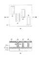
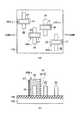
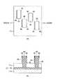
図1および図2(a),(b)は、本発明の第1の実施形態にしたがった、立体構造を有するMOSトランジスタの構成例を示すものである。なお、ここでは、6つのトランジスタからなるSRAM(Static Random Access Memory)セルを構成する場合を例に説明する。また、図1は斜視図、図2(a)は平面図であり、図2(b)は図2(a)のIIB−IIB線に沿う断面図である。[First Embodiment]
FIG. 1 and FIGS. 2A and 2B show a configuration example of a MOS transistor having a three-dimensional structure according to the first embodiment of the present invention. Here, a case where an SRAM (Static Random Access Memory) cell including six transistors is configured will be described as an example. 1 is a perspective view, FIG. 2A is a plan view, and FIG. 2B is a cross-sectional view taken along line IIB-IIB in FIG. 2A.
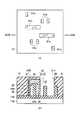
この実施形態の場合、たとえば図1および図2(a)に示すように、SOI(Silicon on Insulator)基板11上に4つの突起部20A,20B,20C,20Dが設けられている。4つの突起部20A,20B,20C,20Dのそれぞれは、たとえば図2(b)に示すように、2つのトランジスタ部(n型MOSトランジスタまたはp型MOSトランジスタ)21,22が1つのゲート電極23を共有してなる構造とされている。 In the case of this embodiment, for example, as shown in FIGS. 1 and 2A, four
すなわち、上記SOI基板11のシリコン(Si)基板11a上には、埋め込み酸化膜(BOX)層11bを介して、4つの絶縁膜層24が設けられている。各絶縁膜層24は、上記BOX層11bの表面に対して、ほぼ垂直方向にそれぞれ起立した状態で設けられている。この絶縁膜層24は、それぞれ、ほぼT字形状の断面を有するとともに、矩形状の一対の側面を有している。各絶縁膜層24の一対の側面、つまり、各絶縁膜層24の両側面には、それぞれ、第1,第2の半導体膜であるn型またはp型となるシリコン膜製のフィン(Si−フィン)25a,25bが設けられている。Si−フィン25a,25bは、上記各絶縁膜層24の突出部24aの長さとほぼ同じ膜厚(幅)を有して形成されている。そして、上記Si−フィン25a,25bと上記絶縁膜層24とによってそれぞれ構成される突起部を、その上部より挟み込むようにして、上記ゲート電極23が設けられている。このゲート電極23と上記Si−フィン25a,25bとの間には、それぞれ、ゲート絶縁膜26が形成されている。これにより、1つのゲート電極23を2つのトランジスタ部21,22が共有してなる構造の、4つの突起部20A,20B,20C,20Dがそれぞれ構成されている。なお、上記した2つのトランジスタ部21,22において、上記ゲート電極23に対応する上記Si−フィン25a,25bにはゲート領域が形成されている。また、上記Si−フィン25a,25bにおける上記ゲート領域の両側には、それぞれ、ソース領域およびドレイン領域が形成されている。 That is, four
このような構成とした場合、4つの突起部20A,20B,20C,20Dにおいて、各チャネル(トランジスタ部21,22)を流れる電流の方向は、上記SOI基板11の表面とほぼ平行となる。なお、上記SOI基板11は、Si基板11a上にBOX層11bを介して、上記Si−フィン25a,25bとなるSi層11cが設けられてなる構成とされている。 In such a configuration, the direction of current flowing through each channel (
ここで、図3(a),(b)〜図7(a),(b)を参照して、突起部20A,20B,20C,20Dの形成方法について説明する。まず、SOI基板11上に第1の絶縁膜、たとえばシリコン窒化(SiN)膜31を堆積する。リソグラフィー工程およびRIE工程により、上記絶縁膜層24の形成領域に対応するSiN膜31とSi層11cとをエッチングする。Si層11cは、上記BOX層11bに達するまでエッチングされる。これにより、上記Si層11cには、長方形状の平面を有するくぼみ部(開口部)32が形成される。次いで、残されたSiN膜31をwetエッチング、たとえばリン酸により、形成しようとするSi−フィン25a,25bの幅に応じた分だけ後退(プルバック)させる。次いで、上記Si層11cに形成されたくぼみ部32内とSiN膜31の後退により形成されたプルバック形成部32a内とを、第2の絶縁膜、たとえばTEOS(Tetra Ethoxy Silane)膜33で埋め込む(以上、図3(a),(b)参照)。 Here, with reference to FIG. 3 (a), (b)-FIG. 7 (a), (b), the formation method of
次に、上記TEOS膜33をレジスト34によってマスクする。このとき、TEOS膜33の長手方向の両端に、上記プルバック形成部32aの長さ(Si−フィン25a,25bの幅)よりも長い非マスク領域34aが形成されるようにする(図4(a),(b)参照)。次に、このレジスト34をマスクに、非マスク領域34aのTEOS膜33をSiN膜31の膜厚の分だけエッチングする(図5(a),(b)参照)。次に、レジスト34を剥離した後、SiN膜31をリン酸によりエッチングして除去し、上記絶縁膜層24を形成する(図6(a),(b)参照)。次に、絶縁膜層24をそれぞれマスクに、Si層11cをエッチングし、その下のBOX層11bを露出させる。これにより、絶縁膜層24の両側面に、それぞれ、突出部24aの長さに応じた幅をもつ、Si層11cからなる薄いSi−フィン25a,25bが形成される(図7(a),(b)参照)。 Next, the TEOS
このように、ほぼT字形状の断面を有する絶縁膜層24をマスクに、Si層11cをRIE処理することにより、絶縁膜層24の第1,第2の側面のみに膜厚の薄いSi層11cを残すことができる。すなわち、上記した方法によれば、絶縁膜層24の一対の側面に、突出部24aに応じた長さ(たとえば、数十オングストローム)程度まで幅の細いSi−フィン25a,25bをもつ構造を得ることが可能である。 As described above, the
続いて、酸化処理などによりSi−フィン25a,25bの側面にそれぞれゲート絶縁膜26を形成した後、ゲート電極材料、たとえばポリシリコン(poly−Si)を全面に堆積させる。そして、そのポリシリコンを、リソグラフィー工程とRIE工程とによりエッチングして、所望のゲート電極23を形成する。これにより、図1および図2(a),(b)に示した構造のMOSトランジスタ(突起部20A,20B,20C,20D)がそれぞれ完成する。 Subsequently, after the
なお、各突起部20A,20B,20C,20Dは、Si−フィン25a,25bのそれぞれが、ゲート電極23の非形成部に対するイオン注入法(I/I)などにより、所望の導電型(n型またはp型)に設定される。これにより、1つのゲート電極23を共有する2つのトランジスタ部21,22が、それぞれ独立したMOSトランジスタとして機能する。つまり、各突起部20A,20B,20C,20Dは、2つのトランジスタ部21,22が共にn型、または、共にp型、もしくは、いずれか一方がn型で、他方がp型のMOSトランジスタとなる。 Each of the
上記したように、ゲート長よりも幅の細いSi−フィンを形成できるようになる。すなわち、SOI基板に対し、ほぼ垂直なリソグラフィー工程の限界よりも膜厚の薄い、たとえば数十オングストローム程度の幅を有するSi−フィンを形成できるようになる。これにより、短チャネル効果が抑制された、完全空乏型の立体構造を有するMOSトランジスタを形成することが可能である。また、この構成によれば、Si−フィンの幅を容易に制御できる。そのため、Si−フィンの寸法ばらつきを少なくすることが可能となり、トランジスタ特性のそろった多数の突起部を製造できる。 As described above, it is possible to form Si-fins that are narrower than the gate length. That is, it becomes possible to form Si-fins having a thickness smaller than the limit of the lithography process substantially perpendicular to the SOI substrate, for example, a width of about several tens of angstroms. Thereby, it is possible to form a MOS transistor having a fully depleted three-dimensional structure in which the short channel effect is suppressed. Further, according to this configuration, the width of the Si-fin can be easily controlled. Therefore, it is possible to reduce the dimensional variation of the Si-fin, and a large number of protrusions having uniform transistor characteristics can be manufactured.
しかも、本実施形態にしたがった構成の場合、SOI基板にほぼ垂直な、たとえば数十nm程度の膜厚を有する絶縁膜層の一対の側面に、ゲート長よりも幅の細いSi−フィンを形成するようにしている。このため、ゲート長よりも幅の細いSi−フィンであっても横倒に強く、かつ、Si−フィンの高さを容易に高くすることが可能であり、トランジスタの電流駆動能力を高める場合などにおいて、特に好適である。 In addition, in the configuration according to the present embodiment, Si-fins that are narrower than the gate length are formed on a pair of side surfaces of an insulating film layer having a thickness of, for example, about several tens of nanometers, which is substantially perpendicular to the SOI substrate. Like to do. For this reason, even if the Si-fin having a width smaller than the gate length is strong on the side, the height of the Si-fin can be easily increased, and the current drive capability of the transistor is increased. Is particularly suitable.
特に、RIEやCMPなどのプロセスにおけるキャップ層やストッパー層の幅を広くとることが可能となるため、プロセス耐性を向上できる。また、ゲート電極を基板上に引き出したりすることなく、突起部の上面にて、直接、メタルプラグをゲート電極と接続することも可能で、面積の縮小化に好適である。 In particular, since it is possible to increase the width of the cap layer and the stopper layer in processes such as RIE and CMP, process resistance can be improved. In addition, the metal plug can be directly connected to the gate electrode on the upper surface of the protruding portion without pulling out the gate electrode onto the substrate, which is suitable for reducing the area.
なお、上記ゲート電極23としては、ダマシン構造のゲート電極を採用することも可能である。また、ゲート絶縁膜26は、CVD(Chemical Vapour Deposition)法またはスパッタリング法によっても形成できる。 The
[第2の実施形態]
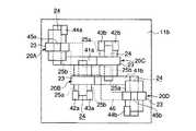
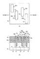
図8は、本発明の第2の実施形態にしたがった、6つのトランジスタにより構成されるSRAMセルの一例を示すものである。ここでは、第1の実施形態に示した4つのT字形状を有する絶縁膜層と2つの半導体膜(Si−フィン)とを備える突起部を用いて、1つのSRAMセルを構成する場合について説明する。[Second Embodiment]
FIG. 8 shows an example of an SRAM cell composed of six transistors according to the second embodiment of the present invention. Here, a case where one SRAM cell is configured by using the protrusions including the four T-shaped insulating film layers and the two semiconductor films (Si-fins) shown in the first embodiment will be described. To do.
4つの突起部20A,20B,20C,20Dを用いて、1つのSRAMセルを構成する場合、たとえば図9に示すように、突起部20Aのトランジスタ部22、突起部20Bのトランジスタ部21、突起部20Cのトランジスタ部22、および、突起部20Dのトランジスタ部21が、それぞれn型MOSトランジスタとされる。また、突起部20Bのトランジスタ部22および突起部20Cのトランジスタ部21が、それぞれp型MOSトランジスタとされる。 When one SRAM cell is configured using the four
すなわち、本実施形態の場合、少なくとも、突起部20Aはn型のSi−フィン25bを有し、突起部20Bはn型のSi−フィン25aおよびp型のSi−フィン25bを有し、突起部20Cはp型のSi−フィン25aおよびn型のSi−フィン25bを有し、突起部20Dはn型のSi−フィン25aを有している。なお、突起部20AのSi−フィン25a(トランジスタ部21)および突起部20DのSi−フィン25b(トランジスタ部22)は、多数のSRAMセルを形成する場合にそれぞれn型とされて、隣接する他のSRAMセルによって利用される。 That is, in this embodiment, at least the
そして、たとえば図8に示したように、突起部20Bのn型Si−フィン25aとp型Si−フィン25bとの一端が、第2の配線層であるメタル配線41aにより接続されている。上記n型Si−フィン25aの他端にはVssコンタクト42aが、上記p型Si−フィン25bの他端にはVddコンタクト43aが、それぞれ接続されている。これにより、突起部20Bにおける2つのトランジスタ部21,22からなる、第1のインバータ回路が構成されている。 For example, as shown in FIG. 8, one end of the n-type Si-
同様に、突起部20Cのp型Si−フィン25aとn型Si−フィン25bとの一端が、第2の配線層であるメタル配線41bにより接続されている。上記p型Si−フィン25aの他端にはVddコンタクト43bが、上記n型Si−フィン25bの他端にはVssコンタクト42bが、それぞれ接続されている。これにより、突起部20Cにおける2つのトランジスタ部21,22からなる、第2のインバータ回路が構成されている。 Similarly, one end of the p-type Si-
また、上記メタル配線41aは、突起部20Cのゲート電極23に接続されている。上記メタル配線41bは、突起部20Bのゲート電極23に接続されている。これにより、2つの突起部20B,20Cからなる、セルデータを保持するためのラッチ回路が構成されている。 The
さらに、上記メタル配線41aは、突起部20Aのn型Si−フィン25bの一端側に接続されている。ゲート電極23を挟んで、このn型Si−フィン25bの他端側には、ビット線コンタクト44aが接続されている。同様に、上記メタル配線41bは、突起部20Dのn型Si−フィン25aの一端側に接続されている。ゲート電極23を挟んで、このn型Si−フィン25aの他端側には、ビット線コンタクト44bが接続されている。 Further, the
そして、突起部20A,20Dの各ゲート電極23,23には、それぞれ、ワード線コンタクト45a,45bが接続されている。また、突起部20A,20Dの各ゲート電極23,23が、上層配線46により相互に接続されて、2つのトランスファ・トランジスタが構成されている。
このように、4つの突起部20A,20B,20C,20Dにより、1つのラッチ回路と2つのトランスファ・トランジスタと備える、6トランジスタ構造のSRAMセルを製造できる。このSRAMセルの場合、RIEやCMPなどのプロセスにおけるキャップ層やストッパー層の幅を広くとることが可能となるため、プロセス耐性を向上できる。また、ゲート電極に対し、突起部の上面にて、直接、メタルプラグ(ワード線コンタクト45a,45b)を接続することが可能となり、セル面積の縮小化に好適である。 As described above, a six-transistor SRAM cell including one latch circuit and two transfer transistors can be manufactured by the four
さらに、各コンタクト42a,42b,43a,43b,44a,44bは、Si−フィン25a,25bの水平方向および垂直方向の各面とのコンタクトにより、より確実なコンタクトが可能である。 Furthermore, each
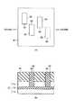
以下に、上記したSRAMセルの製造方法について説明する。その前に、ゲート電極の形成方法およびゲート電極の側壁部分に対するサイドウォール(側壁絶縁膜)の形成方法について、具体的に説明する。すなわち、実際にSRAMセルを製造する場合、ゲート電極の形成にともなって側壁絶縁膜の形成が行われる。 A method for manufacturing the above SRAM cell will be described below. Before that, a method for forming a gate electrode and a method for forming a sidewall (side wall insulating film) on a side wall portion of the gate electrode will be specifically described. That is, when an SRAM cell is actually manufactured, a sidewall insulating film is formed with the formation of the gate electrode.
まず、上記Si−フィン25a,25bの側面にゲート絶縁膜26を形成した後、突起部20A,20B,20C,20Dの相互間を第3の絶縁膜、たとえばBSG(Boron−Silicate Glass)膜51で埋め込む。そして、そのBSG膜51の表面を、CMP工程により平坦化する(図10(a),(b)参照)。次に、ゲート電極23の形成領域にそれぞれ対応する上記BSG膜51を、リソグラフィー工程とRIE工程とにより除去し、開口部52を形成する(図11(a),(b)参照)。次に、その開口部52内が埋まるように、たとえばCVD法により、ポリシリコン53を堆積させる。そして、そのポリシリコン53の表面をCMP工程により平坦化する(図12(a),(b)参照)。 First, after forming the
そして、突起部20A,20B,20C,20Dの相互間に残るBSG膜51を選択的にエッチングし、ポリシリコン53を露出させる。これにより、たとえば図2(a),(b)に示したような、Si−フィン25a,25bと絶縁膜層24とによってそれぞれ構成される突起部を、その上部から挟み込む形のゲート電極23が形成される。また、この状態において、ゲート電極23をマスクに、SOI基板11にほぼ垂直な上記Si−フィン25a,25bに対してI/Iを行い、エクステンション領域(図示していない)を形成する。 Then, the
次に、突起部20A,20B,20C,20Dの相互間を、再度、たとえばBSG膜(第4の絶縁膜)55により埋め込み、CMP工程によって、その表面を平坦化する(図13(a),(b)参照)。次に、BSG膜55の表面をエッチングバックし、ゲート電極23の一部を露出させる(図14(a),(b)参照)。次に、側壁絶縁膜の一部となる第5の絶縁膜、たとえば上記BSG膜55とはエッチング時の選択比が異なるSiN膜56を堆積させる。その後に、このSiN膜56のエッチングを行って、側壁残しによりゲート電極23の周囲部にのみSiN膜56を残す(図15(a),(b)参照)。次に、このSiN膜56をマスクに、上記BSG膜55を選択的にエッチングする。これにより、ゲート電極23の周囲部のみにBSG膜55が残り、上記SiN膜56と上記BSG膜55とからなる側壁絶縁膜57が形成される(図16(a),(b)参照)。 Next, the spaces between the
そして、この状態において、上記側壁絶縁膜57をマスクに、SOI基板11にほぼ垂直な上記Si−フィン25a,25bの側面に対してI/Iを行う。これにより、上記したように、n型またはp型のSi−フィン25a,25bが形成される。その後、コバルト(Co)などをスパッタし、シリサイド化(Silicidation)を行う。これにより、側壁絶縁膜57によって覆われていないSi−フィン25a,25bの側面のみに、シリサイド膜(図示していない)が形成される。このように、n型またはp型のSi−フィン25a,25bの形成およびシリサイド膜の形成は、上記側壁絶縁膜57をマスクに自己整合的に行われる。 In this state, using the
なお、上記した本実施形態においては、Si−フィン25a,25bと絶縁膜層24とによって構成される突起部20A,20B,20C,20Dを例に、側壁絶縁膜の形成方法について説明した。これに限らず、たとえば図17(a),(b)に示すように、1つのSi−フィン25のみにより形成されてなる構成の突起部(立体構造を有するMOSトランジスタ)20A-1,20B-1,20C-1,20D-1の場合にも、本形成方法は同様に適用できる。In the above-described embodiment, the method for forming the sidewall insulating film has been described by taking the
上記した製造方法によれば、突起部において、ゲート電極を形成する際に、Si−フィンの非ゲート領域にあるゲート電極材料を取り除く必要がない。よって、オーバーエッチングによる基板のエッチングやSi−フィンの上面のキャップ層がすべてエッチングされることによる不具合を回避できる。 According to the manufacturing method described above, it is not necessary to remove the gate electrode material in the non-gate region of the Si-fin when forming the gate electrode in the protrusion. Therefore, it is possible to avoid problems caused by etching of the substrate by overetching or etching of the cap layer on the upper surface of the Si-fin.
また、側壁絶縁膜の形成においては、形成領域を除く領域の絶縁膜の除去が容易であるため、Si−フィンの側面を完全に露出させることができ、Si−フィンのシリサイド化をより均一に行うことが可能となる。つまり、オーバーエッチングを必要とすることなしに、ゲート電極の周囲のみに側壁絶縁膜を形成できるようになる。したがって、ソース領域およびドレイン領域の形成およびシリサイド化を、その側壁絶縁膜をマスクに自己整合的に行うことが可能となる。 In addition, in the formation of the sidewall insulating film, since it is easy to remove the insulating film in the region excluding the formation region, the side surface of the Si-fin can be completely exposed, and the silicidation of the Si-fin can be made more uniform. Can be done. That is, the side wall insulating film can be formed only around the gate electrode without requiring overetching. Accordingly, the source region and the drain region can be formed and silicided in a self-aligned manner using the sidewall insulating film as a mask.
上記のように、適宜、n型MOSトランジスタおよびp型MOSトランジスタを作り分けた後(たとえば、図9参照)、SRAMセルは以下のようにして製造される。まず、4つの突起部20A,20B,20C,20Dの相互間を絶縁膜、たとえばBSG膜61により埋め込み、その表面を平坦化する(図18(a),(b)参照)。次に、上記メタル配線41a,41bの形成個所および上記各コンタクト42a,42b、43a,43b、44a,44bの形成個所にそれぞれ対応する上記BSG膜61を、リソグラフィー工程とRIE工程とによって除去し、開口部61aをそれぞれ形成する(図19(a),(b)参照)。次に、上記各開口部61a内にメタル62を埋め込み、平坦化を行う(図20(a),(b)参照)。これにより、上記メタル配線41a,41bおよび上記Vssコンタクト42a,42b、上記Vddコンタクト43a,43b、上記ビット線コンタクト44a,44bが、それぞれ形成される。 As described above, after appropriately forming the n-type MOS transistor and the p-type MOS transistor (see, for example, FIG. 9), the SRAM cell is manufactured as follows. First, the four
次に、全面に層間絶縁膜、たとえばTEOS膜63を堆積させる。そして、上記ワード線コンタクト45a,45bの形成箇所および上記上層配線46の形成箇所にそれぞれ対応する上記TEOS膜63を除去し、開口部63aおよび溝部63bを形成する(図21(a),21(b)参照)。このとき、上記溝部63bは、上層配線46が上記Vssコンタクト42a,42bおよび上記Vddコンタクト43a,43bなどと交わらないようにして形成される。次に、その開口部63a内および溝部63b内に、ダマシン法などによりメタル64を埋め込み、上記上層配線46を形成するとともに、上記ワード線コンタクト45a,45b間を接続させる(図22(a),(b)参照)。 Next, an interlayer insulating film such as a
最後に、上記Vssコンタクト42a,42bのVss配線(図示していない)との接続、上記Vddコンタクト43a,43bのVdd配線(図示していない)との接続、および、上記ビット線コンタクト44a,44bのビット線(図示していない)との接続がそれぞれ行われる。これにより、たとえば図8に示した構成の、4つの突起部20A,20B,20C,20Dからなる6トランジスタ構造のSRAMセルが完成する。 Finally, the
本実施形態の場合、突起部(絶縁膜層およびSi−フィン)の上面において、ゲート電極に対するメタルプラグ(ワード線コンタクト45a,45b)の接続が可能となる。その結果、セル面積を縮小化(小面積化)できる。 In the case of the present embodiment, the metal plugs (
図23は、上記したように、4つの突起部を用いてそれぞれ構成される複数のSRAMセルを、集積化するようにした場合の例を示すものである。複数のSRAMセルを集積化する場合、たとえば図23に示すように、2つのSi−フィン25a,25bと1つの絶縁膜層24とからなる複数の突起部20のうち、一部の突起部20aを長く形成する。また、この長い突起部20aを互いに平行に配置し、各突起部20aに多くのトランスファ・トランジスタを形成する。このような構成とした場合、複数のSRAMセルを、突起部20よりも長い突起部20aの長手方向に集積することが可能となる。 FIG. 23 shows an example in which a plurality of SRAM cells each constituted by using four protrusions are integrated as described above. When integrating a plurality of SRAM cells, for example, as shown in FIG. 23, some of the plurality of
なお、この例の場合、各突起部20,20a、各メタル配線41a,41b、および、各ゲート電極23の相互間には絶縁膜20bが埋め込まれる。そのため、複数のSRAMセルを集積した場合においても、不要な短絡を防ぐことができる。 In the case of this example, an insulating
このように、Si−フィンは幅が細くとも強度が高く、横倒れしにくい。そのため、Si−フィンの高さのみならず、Si−フィンの長さをも容易に長くすることが可能である。よって、突起部を集積する場合、たとえばSRAMセルを集積する場合においては、特に、レイアウト的に有利である。 Thus, even if the Si-fin is thin, the strength is high, and it is difficult for the Si-fin to fall sideways. Therefore, not only the height of the Si-fin but also the length of the Si-fin can be easily increased. Therefore, when integrating the protrusions, for example, when integrating SRAM cells, it is particularly advantageous in terms of layout.
[第3の実施形態]
図24(a),(b)〜図27(a),(b)は、本発明の第3の実施形態にしたがった、突起部の他の構成例を示すものである。ここでは、上記した2つのSi−フィンと1つの絶縁膜層とからなる突起部の製造に、Si製のバルク(bulk)基板を用いるようにした場合について説明する。[Third Embodiment]
24 (a), (b) to FIG. 27 (a), (b) show other configuration examples of the protrusions according to the third embodiment of the present invention. Here, a case will be described in which a Si bulk substrate is used for the manufacture of the protrusions composed of the two Si-fins and one insulating film layer.
バルク基板70を用いる場合、たとえば図24(a),(b)に示すように、あらかじめ、n型MOSトランジスタを形成しようとする個所にはP型ウェル(第1のウェル領域)71を、p型MOSトランジスタを形成しようとする個所にはN型ウェル(第2のウェル領域)72を、それぞれI/Iにより作成する。ウェル71,72を作成しておくことにより、導電型が異なるタイプのSi−フィンの相互間を効果的に素子分離できる。次いで、n型MOSトランジスタおよびp型MOSトランジスタの形成個所にそれぞれ対応させて、突出部を有する絶縁膜層(たとえば、TEOS膜)73を形成する。各絶縁膜層73はほぼT字形状の断面を有し、一対の側面に形成されるSi−フィンの高さよりも長くなるように、それぞれ形成される。これにより、各突起部における2つのSi−フィンの相互間を有効に素子分離できる。 When the
次に、たとえば図25(a),(b)に示すように、絶縁膜層73をマスクに、形成されるSi−フィンの高さに応じて、上記P型ウェル71および上記N型ウェル72をエッチングする。これにより、各絶縁膜層73の両側面の、上記P型ウェル71中および上記N型ウェル72中に、それぞれ、幅の細いSi−フィン74a,74bが形成される。つまり、各絶縁膜層73の一対の側面のみにSi−フィン74a,74bが形成されてなる構成の、4つの突起部70A,70B,70C,70Dが形成される。なお、この例の場合、突起部70AのSi−フィン74a,74bはn型、突起部70BのSi−フィン74aはn型、突起部70BのSi−フィン74bはp型、突起部70CのSi−フィン74aはp型、突起部70CのSi−フィン74bはn型、突起部70DのSi−フィン74a,74bはn型となるように、I/Iなどが行われる。 Next, for example, as shown in FIGS. 25A and 25B, the P-
次に、たとえば図26(a),(b)に示すように、互いに向かい合うSi−フィン74a,74b間の素子分離を行うために、第6の絶縁膜、たとえばSiN膜75を堆積させる。そして、その表面を平坦化する。次に、たとえば図27(a),(b)に示すように、上記SiN膜75を全面エッチバックし、上記P型ウェル71上および上記N型ウェル72上のみにSiN膜75が残るようにする。この場合、残存するSiN膜75は、上記Si−フィン74a,74bの垂直方向の高さに比べて、十分に薄く形成される。これにより、突起部70AのSi−フィン74bと突起部70BのSi−フィン74aとの間、突起部70BのSi−フィン74bと突起部70CのSi−フィン74aとの間、および、突起部70CのSi−フィン74bと突起部70DのSi−フィン74aとの間を、それぞれ素子分離できる。 Next, as shown in FIGS. 26A and 26B, for example, a sixth insulating film, for example, a
しかる後、上記した方法によってゲート電極の形成などが行われる。これにより、ゲート電極の対応する部位にゲート領域、そのゲート領域の両側にそれぞれソース領域およびドレイン領域を有する突起部70A,70B,70C,70Dが完成する。このように、絶縁膜層73の一対の側面にそれぞれゲート長よりも幅の細いSi−フィン74a,74bが形成されてなる構成の突起部70A,70B,70C,70Dを、バルク基板70上に形成することができる。したがって、上述したSOI基板を用いる場合よりもコストの低減が可能である。 Thereafter, the gate electrode is formed by the above-described method. Thus, the
[第4の実施形態]
図28(a),(b)〜図33(a),(b)は、本発明の第4の実施形態にしたがった、突起部のさらに別の構成例を示すものである。ここでは、上記した2つのSi−フィンと1つの絶縁膜層とからなる突起部を、エピタキシャル技術を用いて製造するようにした場合について説明する。[Fourth Embodiment]
FIGS. 28 (a), (b) to 33 (a), (b) show still another configuration example of the protrusion according to the fourth embodiment of the present invention. Here, a description will be given of a case where the protrusions made of the two Si-fins and one insulating film layer are manufactured using an epitaxial technique.
まず、SOI基板11上に、第7の絶縁膜、たとえばBSG膜81を堆積させる。そして、このBSG膜81とその下のSi層11cとを、リソグラフィー工程およびRIE工程により、BOX層11bに達するまでエッチングする。また、上記エッチングにより形成された開口部82内に、第8の絶縁膜、たとえばTEOS膜83を埋め込み、その表面を平坦化する。これにより、TEOS膜83からなる第1の絶縁膜層が形成される(以上、図28(a),(b)参照)。次に、埋め込んだTEOS膜83と上記BSG膜81との間に、所定の空隙部84を形成する。この空隙部84は、たとえばTEOS膜83との境界部にある上記BSG膜81を、リソグラフィー工程とRIE工程とによって、上記Si層11cに達するまで選択的にエッチングすることにより形成される(以上、図29(a),(b)参照)。なお、本実施形態の場合、上記空隙部84は、TEOS膜83の向かい合う一対の側面(第1,第2の側面)にのみ形成されるようになっている。 First, a seventh insulating film, for example, a
次に、上記空隙部84の形成によって露出したSi層11cからのエピタキシャル成長により、上記空隙部84内にSi−フィンとなるエピタキシャル成長層85を形成する。このエピタキシャル成長層85は、上記空隙部84の一部を残して形成される(以上、図30(a),(b)参照)。次に、キャップとなる第9の絶縁膜(第2の絶縁膜層)、たとえばSiN膜86を埋め込み、全面エッチバックを行う。これにより、上記空隙部84内の、上記エピタキシャル成長層85の上部にのみSiN膜86が残存する構造となる(以上、図31(a),(b)参照)。次に、先に堆積させた上記BSG膜81をRIE工程などにより、すべて除去する(図32(a),(b)参照)。 Next, an
次に、上記BSG膜81の除去により露出した上記Si層11cを、RIE工程などによって、Si層11cのみが削れる条件により選択的にエッチングする。これにより、たとえば図33(a),(b)に示すような、2つのSi−フィン85a,85bと、その相互間に設けられた絶縁膜層83とを有してなる構成の突起部が形成される。しかる後、上記した方法によってゲート電極の形成などが行われる。これにより、ゲート電極に対応する部位にゲート領域、そのゲート領域の両側にそれぞれソース領域およびドレイン領域を有する突起部20A’,20B’,20C’,20D’が完成する。 Next, the
本実施形態によっても、上述した第1の実施形態とほぼ同様の効果が得られる。すなわち、SOI基板に対し、ほぼ垂直なリソグラフィー工程の限界よりも膜厚の薄い、たとえば数十オングストローム程度の幅を有するSi−フィンを形成できるようになる。これにより、短チャネル効果が抑制された、完全空乏型の立体構造を有するMOSトランジスタを形成することが可能である。また、この構成によれば、Si−フィンの寸法ばらつきを少なくすることができるので、トランジスタ特性のそろった多数の突起部を製造できる。 Also according to this embodiment, substantially the same effect as that of the first embodiment described above can be obtained. That is, it becomes possible to form Si-fins having a thickness smaller than the limit of the lithography process substantially perpendicular to the SOI substrate, for example, a width of about several tens of angstroms. Thereby, it is possible to form a MOS transistor having a fully depleted three-dimensional structure in which the short channel effect is suppressed. In addition, according to this configuration, it is possible to reduce the dimensional variation of the Si-fin, and thus it is possible to manufacture a large number of protrusions having uniform transistor characteristics.
しかも、本実施形態にしたがった構成においても、SOI基板にほぼ垂直な、たとえば数十nm程度の膜厚を有する絶縁膜層の一対の側面に、ゲート長よりも幅の細いSi−フィンを形成するようにしている。このため、幅の細いSi−フィンであっても横倒に強く、Si−フィンの高さを容易に高くすることが可能で、トランジスタの電流駆動能力を高める場合などにおいて、特に好適である。 Moreover, even in the configuration according to the present embodiment, Si-fins that are narrower than the gate length are formed on the pair of side surfaces of the insulating film layer having a film thickness of approximately several tens of nanometers, for example, approximately perpendicular to the SOI substrate. Like to do. For this reason, even a thin Si-fin is strong sideways, and the height of the Si-fin can be easily increased, which is particularly suitable for increasing the current drive capability of a transistor.
特に、Si−フィンをエピタキシャル成長により形成するようにした本実施形態の場合は、上記した第1および第3の実施形態のように、Si−フィンの形成にRIEなどのプロセスを用いる場合と比べて、チャネルとなるSi−フィンの側面の面方位のばらつきが少なく、また、表面のラフネスも少なくなる。そのため、上述した第1および第3の実施形態よりも、トランジスタ特性の向上が可能である。 In particular, in the case of the present embodiment in which Si-fins are formed by epitaxial growth, as compared with the case of using a process such as RIE for forming Si-fins as in the first and third embodiments described above. The variation in the surface orientation of the side surface of the Si-fin serving as the channel is small, and the roughness of the surface is also small. Therefore, the transistor characteristics can be improved as compared with the first and third embodiments described above.
[第5の実施形態]
図34は、本発明の第5の実施形態にしたがった、6つのトランジスタにより構成されるSRAMセルの他の例を示すものである。ここでは、2つの突起部を用いて、1つのSRAMセルを構成する場合について説明する。[Fifth Embodiment]
FIG. 34 shows another example of an SRAM cell composed of six transistors according to the fifth embodiment of the present invention. Here, a case where one SRAM cell is configured using two protrusions will be described.
それぞれ3つのトランジスタを有する2つの突起部90A,90Bを用いて、1つのSRAMセルを構成する場合、たとえば、突起部90Aのトランジスタ部21a,21b、および、突起部90Bのトランジスタ部22a,22bが、それぞれn型MOSトランジスタとされる。また、突起部90Aのトランジスタ部22、および、突起部90Bのトランジスタ部21が、それぞれp型MOSトランジスタとされる。すなわち、本実施形態の場合、少なくとも、上記突起部90Aはn型のSi−フィン25a(トランジスタ部21a,21b)およびp型のSi−フィン25b(トランジスタ部22)を有し、上記突起部90Bはp型のSi−フィン25a(トランジスタ部21)およびn型のSi−フィン25b(トランジスタ部22a,22b)を有している。 When one SRAM cell is configured using two
そして、突起部90Aのn型Si−フィン25aとp型Si−フィン25bとが、第2の配線層であるメタル配線41aにより接続されている。また、上記n型Si−フィン25aの一端にはVssコンタクト42aが、上記n型Si−フィン25aの他端にはビット線コンタクト44aが、それぞれ接続されている。一方、上記p型Si−フィン25bの一端には、Vddコンタクト43aが接続されている。これにより、突起部90Aにおける3つのトランジスタ部21a,21b,22からなる、第1のインバータ回路および第1のトランスファ・トランジスタが構成されている。同様に、突起部90Bのp型Si−フィン25aとn型Si−フィン25bとが、第2の配線層であるメタル配線41bにより接続されている。また、上記n型Si−フィン25bの一端にはVssコンタクト42bが、上記n型Si−フィン25bの他端にはビット線コンタクト44bが、それぞれ接続されている。一方、上記p型Si−フィン25aの一端には、Vddコンタクト43bが接続されている。これにより、突起部90Bにおける3つのトランジスタ部21,22a,22bからなる、第2のインバータ回路および第2のトランスファ・トランジスタが構成されている。 Then, the n-type Si-
ここで、上記突起部90A,90Bには、それぞれ、Si−フィン25a,25bと絶縁膜層24とによって構成される突起部を、その上部より挟み込むようにして、2つのゲート電極23a,23bが設けられている。つまり、2つのゲート電極23a,23bは、1つの突起部を互いに共有するように設けられている。そして、上記メタル配線41aは、突起部90Bの一方のゲート電極、たとえばゲート電極23aに接続されている。また、上記メタル配線41bは、突起部90Aの一方のゲート電極、たとえばゲート電極23bに接続されている。また、上記突起部90Aのゲート電極23aにはワード線コンタクト45aが、上記突起部90Bのゲート電極23bにはワード線コンタクト45bが、それぞれ接続されている。そして、上記突起部90Aのゲート電極23aおよび上記突起部90Bのゲート電極23bの相互が、上層配線46により接続されている。これにより、2つの突起部90A,90BからなるSRAMセルが構成されている。 Here, in the
このように、本実施形態の構成によれば、2つの突起部90A,90Bにより、1つのラッチ回路と2つのトランスファ・トランジスタとを備える、6トランジスタ構造のSRAMセルを製造できる。すなわち、Si−フィン25a,25bと絶縁膜層24とによって構成される2つの突起部を一直線上に配置して、2つの突起部90A,90Bをそれぞれ構成する。これにより、SRAMセルを構成するのに必要な6つのトランジスタを効率的に配置することが可能となる。したがって、上述した第2の実施形態で示した構成のSRAMセルよりも、さらにセル面積を縮小化できる。 As described above, according to the configuration of the present embodiment, an SRAM cell having a six-transistor structure including one latch circuit and two transfer transistors can be manufactured by the two
図35は、上記した2つの突起部90A,90Bを用いてそれぞれ構成される複数のSRAMセル90を、集積化するようにした場合の例を示すものである。この場合、たとえば図35に示すように、上下方向に関して、1つのビット線コンタクト44を2つのSRAMセル90,90により共有できるように、互いのSRAMセル90,90を構成して配置する。すなわち、一方のSRAMセル90のビット線コンタクト44aと他方のSRAMセル90のビット線コンタクト44bとを互いに共有できるように、2つのSRAMセル90,90を配置する。このような構成とすることにより、セル面積のより一層の縮小化が可能となる。 FIG. 35 shows an example in which a plurality of
なお、便宜上、複数のSRAMセル90(突起部90A,90B)の相互間に埋め込まれる絶縁膜、および、ゲート電極23a,23bの相互を接続するための上層配線については、省略している。 For convenience, the insulating film embedded between the plurality of SRAM cells 90 (
その他、本願発明は、上記(各)実施形態に限定されるものではなく、実施段階ではその要旨を逸脱しない範囲で種々に変形することが可能である。さらに、上記(各)実施形態には種々の段階の発明が含まれており、開示される複数の構成要件における適宜な組み合わせにより種々の発明が抽出され得る。たとえば、(各)実施形態に示される全構成要件からいくつかの構成要件が削除されても、発明が解決しようとする課題の欄で述べた課題(の少なくとも1つ)が解決でき、発明の効果の欄で述べられている効果(の少なくとも1つ)が得られる場合には、その構成要件が削除された構成が発明として抽出され得る。 In addition, the present invention is not limited to the above (each) embodiment, and various modifications can be made without departing from the scope of the invention in the implementation stage. Further, the above (each) embodiment includes various stages of the invention, and various inventions can be extracted by appropriately combining a plurality of disclosed constituent elements. For example, even if several constituent requirements are deleted from all the constituent requirements shown in the (each) embodiment, the problem (at least one) described in the column of the problem to be solved by the invention can be solved. When the effect (at least one of the effects) described in the “Effect” column is obtained, a configuration from which the constituent requirements are deleted can be extracted as an invention.
11…SOI基板、11a…Si基板、11b…埋め込み酸化膜(BOX)層、11c…シリコン(Si)層、20…突起部、20a…長い突起部、20b…絶縁膜、20A,20A’,20B,20B’,20C,20C’,20D,20D’…突起部、21,21a,21b,22,22a,22b…トランジスタ部、23…ゲート電極、24…絶縁膜層、24a…突出部、25,25a,25b…Si−フィン、26…ゲート絶縁膜、31,56…シリコン窒化(SiN)膜、32…くぼみ部、32a…プルバック形成部、33,63…TEOS膜、34…レジスト、34a…非マスク領域、41a,41b…メタル配線、42a,42b…Vddコンタクト、43a,43b…Vssコンタクト、44a,44b…ビット線コンタクト、45a,45b…ワード線コンタクト、46…上層配線、51,55,61…BSG膜、52,61a,63a…開口部、53…ポリシリコン、57…側壁絶縁膜、62,64…メタル、70…バルク基板、70A,70B,70C,70D…突起部、71…P型ウェル、72…N型ウェル、73…絶縁膜層、74a,74b…Si−フィン、75…SiN膜、81…BSG膜、82…開口部、83…TEOS膜(絶縁膜層)、84…空隙部、85…エピタキシャル成長層、85a,85b…Si−フィン、86…SiN膜。 DESCRIPTION OF
Claims (5)
Translated fromJapanese前記第1の絶縁膜および前記半導体層を選択的にエッチングして、長方形状の平面を有する開口部を形成する工程と、
前記第1の絶縁膜を選択的にエッチングして、第1および第2の半導体膜の幅に応じたプルバック部を形成する工程と、
前記開口部および前記プルバック部を第2の絶縁膜により埋め込んで、T字形状の断面を有する絶縁膜層を形成する工程と、
前記第1の絶縁膜をすべて除去した後、前記絶縁膜層をマスクに前記半導体層をエッチングし、前記絶縁膜層の第1および第2の側面に、ゲート長よりも幅の細い前記第1および第2の半導体膜を形成する工程と、
前記絶縁膜層および前記第1および第2の半導体膜を、それぞれ上部より挟み込むようにしてゲート電極を形成する工程と
を具備したことを特徴とする半導体装置の製造方法。On abase plate, depositing a first insulating film over the semiconductorlayer,
Selectively etching the first insulating film and the semiconductorlayer to forman openinghaving arectangular plane ;
Selectively etching the first insulating film to forma pullback portion corresponding to the width of the first and second semiconductor films ;
Filling the opening and thepullback portion with a second insulating film to form an insulating film layer having a T-shapedcross section ;
After removing all the first insulating film, said insulating film layer by etching the semiconductorlayer as a mask, the the first and second side surfaces of the insulating film layer, the thinfirst width than the gate length And forming a second semiconductor film;
Forming a gate electrode so as to sandwich the insulating film layer and the first and second semiconductor films from above, respectively.
Priority Applications (4)
| Application Number | Priority Date | Filing Date | Title |
|---|---|---|---|
| JP2004111095AJP3860582B2 (en) | 2003-07-31 | 2004-04-05 | Manufacturing method of semiconductor device |
| US10/835,122US7164175B2 (en) | 2003-07-31 | 2004-04-28 | Semiconductor device with silicon-film fins and method of manufacturing the same |
| TW093120942ATWI277200B (en) | 2003-07-31 | 2004-07-14 | Semiconductor device and manufacturing method thereof |
| US11/637,734US7541245B2 (en) | 2003-07-31 | 2006-12-12 | Semiconductor device with silicon-film fins and method of manufacturing the same |
Applications Claiming Priority (2)
| Application Number | Priority Date | Filing Date | Title |
|---|---|---|---|
| JP2003204386 | 2003-07-31 | ||
| JP2004111095AJP3860582B2 (en) | 2003-07-31 | 2004-04-05 | Manufacturing method of semiconductor device |
Publications (2)
| Publication Number | Publication Date |
|---|---|
| JP2005064459A JP2005064459A (en) | 2005-03-10 |
| JP3860582B2true JP3860582B2 (en) | 2006-12-20 |
Family
ID=34106869
Family Applications (1)
| Application Number | Title | Priority Date | Filing Date |
|---|---|---|---|
| JP2004111095AExpired - Fee RelatedJP3860582B2 (en) | 2003-07-31 | 2004-04-05 | Manufacturing method of semiconductor device |
Country Status (3)
| Country | Link |
|---|---|
| US (2) | US7164175B2 (en) |
| JP (1) | JP3860582B2 (en) |
| TW (1) | TWI277200B (en) |
Families Citing this family (25)
| Publication number | Priority date | Publication date | Assignee | Title |
|---|---|---|---|---|
| DE10220923B4 (en)* | 2002-05-10 | 2006-10-26 | Infineon Technologies Ag | Method for producing a non-volatile flash semiconductor memory |
| US7018551B2 (en)* | 2003-12-09 | 2006-03-28 | International Business Machines Corporation | Pull-back method of forming fins in FinFets |
| WO2005119763A1 (en)* | 2004-06-04 | 2005-12-15 | Nec Corporation | Semiconductor device and manufacturing method thereof |
| US7388663B2 (en)* | 2004-10-28 | 2008-06-17 | Asml Netherlands B.V. | Optical position assessment apparatus and method |
| JP2006128494A (en)* | 2004-10-29 | 2006-05-18 | Toshiba Corp | Semiconductor integrated circuit device and manufacturing method thereof |
| JP4648096B2 (en)* | 2005-06-03 | 2011-03-09 | 株式会社東芝 | Manufacturing method of semiconductor device |
| WO2007049170A1 (en)* | 2005-10-25 | 2007-05-03 | Nxp B.V. | Finfet transistors |
| US7547947B2 (en)* | 2005-11-15 | 2009-06-16 | International Business Machines Corporation | SRAM cell |
| JP2007173326A (en)* | 2005-12-19 | 2007-07-05 | Korea Advanced Inst Of Sci Technol | Field effect transistor having channel comprising silicon fin and silicon body and method of manufacturing |
| KR100732304B1 (en)* | 2006-03-23 | 2007-06-25 | 주식회사 하이닉스반도체 | Semiconductor element and manufacturing method thereof |
| US8040717B2 (en) | 2006-12-28 | 2011-10-18 | National Institute Of Advanced Industrial Science And Technology | SRAM cell and SRAM device |
| JP4461154B2 (en)* | 2007-05-15 | 2010-05-12 | 株式会社東芝 | Semiconductor device |
| US7923337B2 (en)* | 2007-06-20 | 2011-04-12 | International Business Machines Corporation | Fin field effect transistor devices with self-aligned source and drain regions |
| US20090001470A1 (en)* | 2007-06-26 | 2009-01-01 | Anderson Brent A | Method for forming acute-angle spacer for non-orthogonal finfet and the resulting structure |
| US20090124097A1 (en)* | 2007-11-09 | 2009-05-14 | International Business Machines Corporation | Method of forming narrow fins in finfet devices with reduced spacing therebetween |
| US8659088B2 (en) | 2008-03-28 | 2014-02-25 | National Institute Of Advanced Industrial Science And Technology | SRAM cell and SRAM device |
| US8582352B2 (en)* | 2011-12-06 | 2013-11-12 | Taiwan Semiconductor Manufacturing Company, Ltd. | Methods and apparatus for FinFET SRAM cells |
| US8693235B2 (en) | 2011-12-06 | 2014-04-08 | Taiwan Semiconductor Manufacturing Company, Ltd. | Methods and apparatus for finFET SRAM arrays in integrated circuits |
| KR20180104195A (en)* | 2011-12-22 | 2018-09-19 | 인텔 코포레이션 | Semiconductor structure |
| US20150188078A1 (en)* | 2012-06-14 | 2015-07-02 | Konica Minolta, Inc. | Electroluminescent Element and Lighting Apparatus Comprising the Same |
| WO2015045207A1 (en)* | 2013-09-27 | 2015-04-02 | パナソニック株式会社 | Semiconductor integrated circuit and semiconductor integrated circuit device |
| US9136384B2 (en)* | 2013-12-05 | 2015-09-15 | Stmicroelectronics, Inc. | Method for the formation of a FinFET device having partially dielectric isolated Fin structure |
| KR102217246B1 (en) | 2014-11-12 | 2021-02-18 | 삼성전자주식회사 | Integrated circuit device and method of manufacturing the same |
| CN106156375B (en)* | 2015-03-24 | 2019-01-04 | 展讯通信(上海)有限公司 | A kind of memory compiler joining method and memory |
| US9466723B1 (en)* | 2015-06-26 | 2016-10-11 | Globalfoundries Inc. | Liner and cap layer for placeholder source/drain contact structure planarization and replacement |
Family Cites Families (13)
| Publication number | Priority date | Publication date | Assignee | Title |
|---|---|---|---|---|
| JPH03187272A (en)* | 1989-12-15 | 1991-08-15 | Mitsubishi Electric Corp | MOS field effect transistor and its manufacturing method |
| JPH04250667A (en) | 1991-01-28 | 1992-09-07 | Oki Electric Ind Co Ltd | Semiconductor device and manufacture thereof |
| JP2789931B2 (en) | 1991-05-27 | 1998-08-27 | 日本電気株式会社 | Semiconductor device |
| US5554870A (en)* | 1994-02-04 | 1996-09-10 | Motorola, Inc. | Integrated circuit having both vertical and horizontal devices and process for making the same |
| EP1486891A3 (en)* | 1997-02-12 | 2005-03-09 | Kokusai Denshin Denwa Co., Ltd | Document retrieval apparatus |
| IL121181A0 (en)* | 1997-06-27 | 1997-11-20 | Agentics Ltd | A method and system for unifying multiple information resources into hierarchial integrated information resource accessible by means of user interface |
| US6073135A (en)* | 1998-03-10 | 2000-06-06 | Alta Vista Company | Connectivity server for locating linkage information between Web pages |
| US6112203A (en)* | 1998-04-09 | 2000-08-29 | Altavista Company | Method for ranking documents in a hyperlinked environment using connectivity and selective content analysis |
| JP4083869B2 (en) | 1998-05-14 | 2008-04-30 | 宮城沖電気株式会社 | Manufacturing method of semiconductor device |
| US6675161B1 (en)* | 1999-05-04 | 2004-01-06 | Inktomi Corporation | Managing changes to a directory of electronic documents |
| WO2000079379A1 (en)* | 1999-06-19 | 2000-12-28 | Kent Ridge Digital Labs | A system of organising catalog data for searching and retrieval |
| US6868525B1 (en)* | 2000-02-01 | 2005-03-15 | Alberti Anemometer Llc | Computer graphic display visualization system and method |
| US6762448B1 (en)* | 2003-04-03 | 2004-07-13 | Advanced Micro Devices, Inc. | FinFET device with multiple fin structures |
- 2004
- 2004-04-05JPJP2004111095Apatent/JP3860582B2/ennot_activeExpired - Fee Related
- 2004-04-28USUS10/835,122patent/US7164175B2/ennot_activeExpired - Fee Related
- 2004-07-14TWTW093120942Apatent/TWI277200B/ennot_activeIP Right Cessation
- 2006
- 2006-12-12USUS11/637,734patent/US7541245B2/ennot_activeExpired - Lifetime
Also Published As
| Publication number | Publication date |
|---|---|
| JP2005064459A (en) | 2005-03-10 |
| US7541245B2 (en) | 2009-06-02 |
| TWI277200B (en) | 2007-03-21 |
| US7164175B2 (en) | 2007-01-16 |
| TW200509374A (en) | 2005-03-01 |
| US20050026377A1 (en) | 2005-02-03 |
| US20070090468A1 (en) | 2007-04-26 |
Similar Documents
| Publication | Publication Date | Title |
|---|---|---|
| JP3860582B2 (en) | Manufacturing method of semiconductor device | |
| TWI772378B (en) | Integrated circuit device and method of manufacturing the same | |
| US8941157B2 (en) | Semiconductor device and method for fabricating the same | |
| TWI458068B (en) | Vertical channel transistor array and manufacturing method thereof | |
| KR100822079B1 (en) | Single cotton buried strap | |
| KR102788536B1 (en) | Integrated circuit device and method of manufacturing the same | |
| KR20070105376A (en) | Method of forming recessed access device | |
| TW202243139A (en) | Dynamic random access memory and method of fabricating the same | |
| TW202215642A (en) | Integrated circuit device | |
| JPS63228742A (en) | 3D 1-transistor memory cell structure and its manufacturing method | |
| US11678477B2 (en) | Semiconductor constructions, and semiconductor processing methods | |
| US6911740B2 (en) | Semiconductor device having increased gaps between gates | |
| US20060011971A1 (en) | Nonvolatile semiconductor memory device and method of manufacturing the same | |
| US20200176454A1 (en) | Integrated Assemblies Which Include Metal-Containing Interconnects to Active-Region Pillars, and Methods of Forming Integrated Assemblies | |
| KR20120085360A (en) | Gate structures, methods of forming gate structures, and methods of manufacturing semiconductor devices using the same | |
| JP2010520645A (en) | Formation of trenches in semiconductor materials | |
| JP2003158206A (en) | Method for manufacturing silicide film of flat cell memory device | |
| KR101087521B1 (en) | Method of fabricating semiconductor device to provide improved separation between contact and cell gate electrode | |
| US6870211B1 (en) | Self-aligned array contact for memory cells | |
| TWI851202B (en) | Integrated circuit device | |
| CN118890896B (en) | Three-dimensional memory and preparation method thereof | |
| CN110943083A (en) | Word line driver and method of making the same | |
| JPH1197529A (en) | Manufacture of semiconductor device | |
| US20250267850A1 (en) | Integrated circuit device and method of manufacturing the same | |
| KR100405936B1 (en) | Method for manufacturing a landing plug of semiconductor device by using selective epitaxial growth |
Legal Events
| Date | Code | Title | Description |
|---|---|---|---|
| A977 | Report on retrieval | Free format text:JAPANESE INTERMEDIATE CODE: A971007 Effective date:20060202 | |
| A131 | Notification of reasons for refusal | Free format text:JAPANESE INTERMEDIATE CODE: A131 Effective date:20060207 | |
| A521 | Request for written amendment filed | Free format text:JAPANESE INTERMEDIATE CODE: A523 Effective date:20060410 | |
| TRDD | Decision of grant or rejection written | ||
| A01 | Written decision to grant a patent or to grant a registration (utility model) | Free format text:JAPANESE INTERMEDIATE CODE: A01 Effective date:20060919 | |
| A61 | First payment of annual fees (during grant procedure) | Free format text:JAPANESE INTERMEDIATE CODE: A61 Effective date:20060921 | |
| FPAY | Renewal fee payment (event date is renewal date of database) | Free format text:PAYMENT UNTIL: 20090929 Year of fee payment:3 | |
| FPAY | Renewal fee payment (event date is renewal date of database) | Free format text:PAYMENT UNTIL: 20100929 Year of fee payment:4 | |
| FPAY | Renewal fee payment (event date is renewal date of database) | Free format text:PAYMENT UNTIL: 20110929 Year of fee payment:5 | |
| FPAY | Renewal fee payment (event date is renewal date of database) | Free format text:PAYMENT UNTIL: 20110929 Year of fee payment:5 | |
| FPAY | Renewal fee payment (event date is renewal date of database) | Free format text:PAYMENT UNTIL: 20120929 Year of fee payment:6 | |
| FPAY | Renewal fee payment (event date is renewal date of database) | Free format text:PAYMENT UNTIL: 20120929 Year of fee payment:6 | |
| FPAY | Renewal fee payment (event date is renewal date of database) | Free format text:PAYMENT UNTIL: 20130929 Year of fee payment:7 | |
| LAPS | Cancellation because of no payment of annual fees |