JP3858849B2 - Semiconductor device and manufacturing method thereof - Google Patents
Semiconductor device and manufacturing method thereofDownload PDFInfo
- Publication number
- JP3858849B2 JP3858849B2JP2003111437AJP2003111437AJP3858849B2JP 3858849 B2JP3858849 B2JP 3858849B2JP 2003111437 AJP2003111437 AJP 2003111437AJP 2003111437 AJP2003111437 AJP 2003111437AJP 3858849 B2JP3858849 B2JP 3858849B2
- Authority
- JP
- Japan
- Prior art keywords
- conductive layer
- opening
- insulating film
- film
- layer
- Prior art date
- Legal status (The legal status is an assumption and is not a legal conclusion. Google has not performed a legal analysis and makes no representation as to the accuracy of the status listed.)
- Expired - Fee Related
Links
- 239000004065semiconductorSubstances0.000titleclaimsdescription58
- 238000004519manufacturing processMethods0.000titleclaimsdescription33
- 238000000034methodMethods0.000claimsdescription61
- 239000000758substrateSubstances0.000claimsdescription35
- 239000010949copperSubstances0.000claimsdescription25
- 229910004298SiO 2Inorganic materials0.000claimsdescription15
- 230000008602contractionEffects0.000claimsdescription14
- 239000012528membraneSubstances0.000claimsdescription10
- YCKRFDGAMUMZLT-UHFFFAOYSA-NFluorine atomChemical compound[F]YCKRFDGAMUMZLT-UHFFFAOYSA-N0.000claimsdescription9
- 229910052731fluorineInorganic materials0.000claimsdescription9
- 239000011737fluorineSubstances0.000claimsdescription9
- 239000004020conductorSubstances0.000claimsdescription4
- 229910052802copperInorganic materials0.000claimsdescription4
- RYGMFSIKBFXOCR-UHFFFAOYSA-NCopperChemical compound[Cu]RYGMFSIKBFXOCR-UHFFFAOYSA-N0.000claimsdescription3
- 239000010410layerSubstances0.000description298
- 239000002184metalSubstances0.000description34
- 229910052751metalInorganic materials0.000description34
- 238000009792diffusion processMethods0.000description27
- 230000004888barrier functionEffects0.000description18
- 230000002265preventionEffects0.000description18
- 230000008569processEffects0.000description17
- 239000000463materialSubstances0.000description15
- ATVJXMYDOSMEPO-UHFFFAOYSA-N3-prop-2-enoxyprop-1-eneChemical compoundC=CCOCC=CATVJXMYDOSMEPO-UHFFFAOYSA-N0.000description13
- 239000011347resinSubstances0.000description13
- 229920005989resinPolymers0.000description13
- 238000005530etchingMethods0.000description9
- 238000001459lithographyMethods0.000description7
- 230000015572biosynthetic processEffects0.000description5
- 230000008859changeEffects0.000description4
- 238000007796conventional methodMethods0.000description4
- 239000011229interlayerSubstances0.000description3
- 238000002955isolationMethods0.000description3
- 238000004544sputter depositionMethods0.000description3
- VYPSYNLAJGMNEJ-UHFFFAOYSA-NSilicium dioxideChemical compoundO=[Si]=OVYPSYNLAJGMNEJ-UHFFFAOYSA-N0.000description2
- 238000009713electroplatingMethods0.000description2
- 238000010438heat treatmentMethods0.000description2
- 238000005498polishingMethods0.000description2
- 230000004913activationEffects0.000description1
- 229910052681coesiteInorganic materials0.000description1
- 229910052906cristobaliteInorganic materials0.000description1
- 238000001312dry etchingMethods0.000description1
- 230000009977dual effectEffects0.000description1
- 230000000694effectsEffects0.000description1
- 229910052737goldInorganic materials0.000description1
- 230000010354integrationEffects0.000description1
- 238000002844meltingMethods0.000description1
- 230000008018meltingEffects0.000description1
- 238000012986modificationMethods0.000description1
- 230000004048modificationEffects0.000description1
- 238000007747platingMethods0.000description1
- 238000004904shorteningMethods0.000description1
- 239000000377silicon dioxideSubstances0.000description1
- 229910052709silverInorganic materials0.000description1
- 239000007779soft materialSubstances0.000description1
- 229910052682stishoviteInorganic materials0.000description1
- 229910052905tridymiteInorganic materials0.000description1
Images


Classifications
- H—ELECTRICITY
- H01—ELECTRIC ELEMENTS
- H01L—SEMICONDUCTOR DEVICES NOT COVERED BY CLASS H10
- H01L21/00—Processes or apparatus adapted for the manufacture or treatment of semiconductor or solid state devices or of parts thereof
- H01L21/70—Manufacture or treatment of devices consisting of a plurality of solid state components formed in or on a common substrate or of parts thereof; Manufacture of integrated circuit devices or of parts thereof
- H01L21/71—Manufacture of specific parts of devices defined in group H01L21/70
- H01L21/768—Applying interconnections to be used for carrying current between separate components within a device comprising conductors and dielectrics
- H01L21/76801—Applying interconnections to be used for carrying current between separate components within a device comprising conductors and dielectrics characterised by the formation and the after-treatment of the dielectrics, e.g. smoothing
- H01L21/76802—Applying interconnections to be used for carrying current between separate components within a device comprising conductors and dielectrics characterised by the formation and the after-treatment of the dielectrics, e.g. smoothing by forming openings in dielectrics
- H01L21/76807—Applying interconnections to be used for carrying current between separate components within a device comprising conductors and dielectrics characterised by the formation and the after-treatment of the dielectrics, e.g. smoothing by forming openings in dielectrics for dual damascene structures
- H01L21/76808—Applying interconnections to be used for carrying current between separate components within a device comprising conductors and dielectrics characterised by the formation and the after-treatment of the dielectrics, e.g. smoothing by forming openings in dielectrics for dual damascene structures involving intermediate temporary filling with material
- A—HUMAN NECESSITIES
- A47—FURNITURE; DOMESTIC ARTICLES OR APPLIANCES; COFFEE MILLS; SPICE MILLS; SUCTION CLEANERS IN GENERAL
- A47J—KITCHEN EQUIPMENT; COFFEE MILLS; SPICE MILLS; APPARATUS FOR MAKING BEVERAGES
- A47J41/00—Thermally-insulated vessels, e.g. flasks, jugs, jars
- A47J41/0083—Accessories
- H—ELECTRICITY
- H01—ELECTRIC ELEMENTS
- H01L—SEMICONDUCTOR DEVICES NOT COVERED BY CLASS H10
- H01L21/00—Processes or apparatus adapted for the manufacture or treatment of semiconductor or solid state devices or of parts thereof
- H01L21/70—Manufacture or treatment of devices consisting of a plurality of solid state components formed in or on a common substrate or of parts thereof; Manufacture of integrated circuit devices or of parts thereof
- H01L21/71—Manufacture of specific parts of devices defined in group H01L21/70
- H01L21/768—Applying interconnections to be used for carrying current between separate components within a device comprising conductors and dielectrics
- H01L21/76801—Applying interconnections to be used for carrying current between separate components within a device comprising conductors and dielectrics characterised by the formation and the after-treatment of the dielectrics, e.g. smoothing
- H01L21/76802—Applying interconnections to be used for carrying current between separate components within a device comprising conductors and dielectrics characterised by the formation and the after-treatment of the dielectrics, e.g. smoothing by forming openings in dielectrics
- H01L21/76807—Applying interconnections to be used for carrying current between separate components within a device comprising conductors and dielectrics characterised by the formation and the after-treatment of the dielectrics, e.g. smoothing by forming openings in dielectrics for dual damascene structures
- H—ELECTRICITY
- H01—ELECTRIC ELEMENTS
- H01L—SEMICONDUCTOR DEVICES NOT COVERED BY CLASS H10
- H01L21/00—Processes or apparatus adapted for the manufacture or treatment of semiconductor or solid state devices or of parts thereof
- H01L21/70—Manufacture or treatment of devices consisting of a plurality of solid state components formed in or on a common substrate or of parts thereof; Manufacture of integrated circuit devices or of parts thereof
- H01L21/71—Manufacture of specific parts of devices defined in group H01L21/70
- H01L21/768—Applying interconnections to be used for carrying current between separate components within a device comprising conductors and dielectrics
- H01L21/76838—Applying interconnections to be used for carrying current between separate components within a device comprising conductors and dielectrics characterised by the formation and the after-treatment of the conductors
- H—ELECTRICITY
- H01—ELECTRIC ELEMENTS
- H01L—SEMICONDUCTOR DEVICES NOT COVERED BY CLASS H10
- H01L23/00—Details of semiconductor or other solid state devices
- H01L23/52—Arrangements for conducting electric current within the device in operation from one component to another, i.e. interconnections, e.g. wires, lead frames
- H01L23/522—Arrangements for conducting electric current within the device in operation from one component to another, i.e. interconnections, e.g. wires, lead frames including external interconnections consisting of a multilayer structure of conductive and insulating layers inseparably formed on the semiconductor body
- A—HUMAN NECESSITIES
- A47—FURNITURE; DOMESTIC ARTICLES OR APPLIANCES; COFFEE MILLS; SPICE MILLS; SUCTION CLEANERS IN GENERAL
- A47J—KITCHEN EQUIPMENT; COFFEE MILLS; SPICE MILLS; APPARATUS FOR MAKING BEVERAGES
- A47J45/00—Devices for fastening or gripping kitchen utensils or crockery
- A47J45/06—Handles for hollow-ware articles
- A47J45/062—Bowl handles
- A—HUMAN NECESSITIES
- A47—FURNITURE; DOMESTIC ARTICLES OR APPLIANCES; COFFEE MILLS; SPICE MILLS; SUCTION CLEANERS IN GENERAL
- A47J—KITCHEN EQUIPMENT; COFFEE MILLS; SPICE MILLS; APPARATUS FOR MAKING BEVERAGES
- A47J47/00—Kitchen containers, stands or the like, not provided for in other groups of this subclass; Cutting-boards, e.g. for bread
- A47J47/02—Closed containers for foodstuffs
- H—ELECTRICITY
- H01—ELECTRIC ELEMENTS
- H01L—SEMICONDUCTOR DEVICES NOT COVERED BY CLASS H10
- H01L2924/00—Indexing scheme for arrangements or methods for connecting or disconnecting semiconductor or solid-state bodies as covered by H01L24/00
- H01L2924/0001—Technical content checked by a classifier
- H01L2924/0002—Not covered by any one of groups H01L24/00, H01L24/00 and H01L2224/00
Landscapes
- Engineering & Computer Science (AREA)
- Physics & Mathematics (AREA)
- Condensed Matter Physics & Semiconductors (AREA)
- General Physics & Mathematics (AREA)
- Computer Hardware Design (AREA)
- Microelectronics & Electronic Packaging (AREA)
- Power Engineering (AREA)
- Manufacturing & Machinery (AREA)
- Thermal Sciences (AREA)
- Food Science & Technology (AREA)
- Internal Circuitry In Semiconductor Integrated Circuit Devices (AREA)
Description
Translated fromJapanese【0001】
【発明の属する技術分野】
本発明は、半導体装置およびその製造方法に関し、特に、絶縁膜に形成された接続孔により複数の導電層を電気的に接続する多層配線を有する半導体装置およびその製造方法に関する。
【0002】
【従来の技術】
LSIの高集積化および高性能化に伴い、素子寸法の微細化および多層構造化が進んでいる。多層配線の微細化により増大する配線遅延を低減するためには、配線抵抗および容量に影響を与えるパラメータ(配線膜厚)、配線容量に影響を与えるパラメータ(層間膜厚、比誘電率)および配線抵抗に影響を与えるパラメータ(配線抵抗率)などを適切な割合でスケーリングする必要がある。
【0003】
配線材料としては、大きな電圧降下なく電気信号を伝播するために抵抗率が低いことが望ましい。従来広く用いられているAlに対し、抵抗率が低いものはAu,Cu,Agなどが挙げられる。なかでも、Cuは、Alよりも融点が高く、エレクトロマイグレーション現象の活性化エネルギーが大きいことからもAlに比べて信頼性が向上することが報告されている。しかし、Cuを微細配線に使用するには、ドライエッチング法において、Cuを下地となる絶縁膜に対して高い選択比でエッチングする適当なガスが存在しないため、一般的に埋設型配線形成技術〔ダマシン(Damascene)法〕によって埋め込み配線を形成する。特に、接続孔と配線とを同時に埋め込むデュアル ダマシン(dual damascene)法は、リソグラフィーにおけるアライメントマージンの拡大や工程短縮化の観点から有用である。
【0004】
また、絶縁膜としては、配線容量低減の観点から、比誘電率の小さいものが望ましい。使用する材料としてはアリルエーテル系樹脂およびSiOCなどに代表される低誘電率材料へと移行している。しかし、アリルエーテル系樹脂などの低誘電率材料は、従来使用されていたSiO2 膜およびフッ素含有のSiO2 膜よりもヤング率が低く、比較的疎な膜である。
【0005】
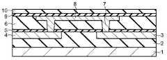
図10は、従来の技術にかかる半導体装置の一部を模式的に示した概略断面図である。半導体基板1の上面に絶縁膜2が形成され、絶縁膜2の上面の一部には配線溝が形成され、その配線溝に第1の導電層3および第2の導電層4が形成されている。第1の導電層3および第2の導電層4が形成された絶縁膜2の上面に拡散防止膜5が形成され、拡散防止膜5の上面に絶縁膜6が形成されている。絶縁膜6の上面の一部に形成された配線溝に第3の導電層8が形成され、第3の導電層8が形成された絶縁膜6の上面に拡散防止膜9が形成され、拡散防止膜9の上面に絶縁膜10が形成されている。さらに、第1の導電層3および第2の導電膜4と第3の導電層8とは、それぞれ開口部7を介して電気的に接続されている。ここで、開口部内は第3の導電層8と同じ材料で埋め込まれている。また、拡散防止膜5,9は、層構成および用いる導電層の材料に応じて形成しなくてもよい。半導体基板1に形成された、素子領域および素子分離領域は図示を省略している。
【0006】
上記のような、従来の半導体装置の製造方法として、基板上に形成された層間絶縁膜と、基板上に形成された上層配線および下層配線と、上層配線と下層配線とを電気的に接続するプラグとを形成し、プラグの近傍の層間絶縁膜中に電流の流路とならない柱を形成することが知られている(たとえば、特許文献1参照)。
【0007】
【特許文献1】
特開平11−154679号公報 (第3−7頁、第1−10図)
【0008】
【発明が解決しようとする課題】
しかしながら、上記のような従来の方法においては、ヤング率の低い絶縁膜を使用しているので、工程中の高温雰囲気下において、導電層の熱膨張あるいは収縮により、導電層の長手方向が伸縮し、容易に変形してしまう。
高温雰囲気下(たとえば、400℃程度)における配線および接続部の変形の一例を図11に示す。
図11は、従来の技術にかかる半導体装置の一部を模式的に示した概略断面図であり、図10の構成の高温時における配線の様子を示している。
図10,11において、1本の長い第3の導電層8が比較的柔らかい低ヤング率の材料で形成された絶縁膜6に形成されているとき、上層部の絶縁膜形成工程や硬化などの高温熱処理工程に、導電層はその配線長に比例して容易に膨張する。通常導電層の端部は下層配線に接続するような開口部が形成されているが、多くの電流を流さない電位固定のために使用される場合は1つの開口部のみが形成される。したがって、第3の導電層8が膨張したときに開口部7の上部が第3の導電層8の長手方向に引っ張られ、その結果、密着性の悪い接続部、つまり接続孔7の底部と下層配線層(図10,11中においては第1の導電層3および第2の導電層4)との界面にて剥がれが生じ、接続孔7は電気的に独立した導電層20となる。
このように、特に脆弱な配線間の接続部において変形し、断線などを生じるので、製品歩留りおよび配線信頼性に対して、大きな影響を与える可能性が考えられる。
【0009】
本発明は、かかる事情に鑑みてなされたものであり、その目的は、導電層の熱膨張あるいは収縮による開口部の変形を抑制し、製品歩留りおよび配線信頼性を向上させる半導体装置およびその製造方法を提供することにある。
【0010】
【課題を解決するための手段】
上記目的を達成するため、上記の本発明の半導体装置は、基板と、前記基板に形成された第1の導電層と、前記第1の導電層と所定の距離を離間して前記基板に形成された第2の導電層と、前記第1の導電層および前記第2の導電層の上面に形成され、前記第1の導電層および前記第2の導電層のいずれかがそれぞれ露出するように形成された複数の第1の開口部と、前記第1の導電層および前記第2の導電層のいずれもが露出しないように形成された第2の開口部とを有し、SiO2膜およびフッ素含有のSiO2膜よりもヤング率が低い絶縁膜と、前記第1の開口部および前記第2の開口部を埋め込むように前記絶縁膜の上面に形成され、前記第1の開口部を介して前記第1の導電層および前記第2の導電層と電気的に接続された第3の導電層とを有し、前記第2の開口部は、前記第3の導電層に沿って2つの前記第1の開口部の間に形成されている。
【0011】
上記の本発明の半導体装置においては、第2の開口部を第3の導電層に沿って、2つの第1の開口部の間に形成することにより、第1の開口部にかかる力を分散し、第1の導電層および第2の導電層のいずれか一方と、第3の導電層との接続部である第1の開口部の変形を抑制する。
【0012】
上記の本発明の半導体装置は、基板と、前記基板に形成された第1の導電層と、前記第1の導電層と所定の距離を離間して前記基板に形成された第2の導電層と、前記第1の導電層および前記第2の導電層の上面に形成され、前記第1の導電層および前記第2の導電層のいずれかの端部がそれぞれ露出するように形成された開口部を有し、SiO2膜およびフッ素含有のSiO2膜よりもヤング率が低い絶縁膜と、前記開口部を埋め込むように前記絶縁膜の上面に形成され、前記第1の導電層および前記第2の導電層と電気的に接続された第3の導電層とを有し、前記第3の導電層は、熱膨張または収縮により長手方向の長さが変化しても接続が保たれるような所定の配線長を有し、前記第3の導電層の両端において、前記第1の導電層および前記第2の導電層と前記開口部を介して電気的に接続されている。
【0013】
上記の本発明の半導体装置においては、第3の導電層を所定の配線長を有することにより、熱膨張または収縮により長手方向の長さが変化しても、第1の導電層および第2の導電層と開口部を介して、電気的に接続が保たれる。
【0014】
本発明の半導体装置の製造方法は、基板に第1の導電層を形成する工程と、前記第1の導電層と所定の距離を離間して前記基板に第2の導電層を形成する工程と、前記第1の導電層および前記第2の導電層の上面にSiO2膜およびフッ素含有のSiO2膜よりもヤング率が低い絶縁膜を形成する工程と、前記絶縁膜に、前記第1の導電層および前記第2の導電層のいずれかがそれぞれ露出するような複数の第1の開口部と、前記第1の導電層および前記第2の導電層いずれもが露出しないような第2の開口部とを形成する工程と、前記第1の開口部および前記第2の開口部を埋め込み、前記第1の開口部を介して前記第1の導電層および前記第2の導電層と電気的に接続するように前記絶縁膜の上面に第3の導電層を形成する工程とを有し、前記第2の開口部は、前記第3の導電層に沿って2つの前記第1の開口部の間に形成する。
【0015】
上記の本発明の半導体装置の製造方法においては、基板に第1の導電層を形成し、第1の導電層と所定の距離を離間して基板に第2の導電層を形成する。第1の導電層および第2の導電層の上面に絶縁膜を形成し、絶縁膜に、第1の導電層および第2の導電層のいずれかがそれぞれ露出するような複数の第1の開口部と、第1の導電層および第2の導電層いずれもが露出しないような第2の開口部とを形成する。第1の開口部および第2の開口部を埋め込み、第1の開口部を介して第1の導電層および第2の導電層と電気的に接続するように絶縁膜の上面に第3の導電層を形成する。ここで、第2の開口部は、第3の導電層に沿って2つの第1の開口部の間に形成する。
【0016】
本発明の半導体装置の製造方法は、基板に第1の導電層を形成する工程と、前記第1の導電層と所定の距離を離間して前記基板に第2の導電層を形成する工程と、前記第1の導電層および前記第2の導電層の上面にSiO2膜およびフッ素含有のSiO2膜よりもヤング率が低い絶縁膜を形成する工程と、前記絶縁膜に前記第1の導電層および前記第2の導電層のいずれかの端部がそれぞれ露出するように開口部を形成する工程と、前記開口部を埋め込み、前記第1の導電層および前記第2の導電層と電気的に接続するように前記絶縁膜の上面に第3の導電層を形成する工程とを有し、前記第3の導電層の配線長は、熱膨張または収縮により長手方向の長さが変化しても接続が保たれるような所定の長さに形成し、前記第3の導電層の両端において、前記第1の導電層および前記第2の導電層と、前記開口部を介して電気的に接続するように形成する。
【0017】
上記の本発明の半導体装置の製造方法においては、基板に第1の導電層を形成し、第1の導電層と所定の距離を離間して基板に第2の導電層を形成する。第1の導電層および第2の導電層の上面に絶縁膜を形成し、絶縁膜に第1の導電層および第2の導電層のいずれかの端部がそれぞれ露出するように開口部を形成する。開口部を埋め込み、第1の導電層および第2の導電層と電気的に接続するように絶縁膜の上面に第3の導電層を形成する。ここで、第3の導電層の配線長は、熱膨張または収縮により長手方向の長さが変化しても接続が保たれるような所定の長さに形成し、第3の導電層の両端において、第1の導電層および第2の導電層と開口部を介して電気的に接続するように形成する。
【0018】
【発明の実施の形態】
以下、本発明の実施形態について図面に基づいて説明する。
〔第1の実施形態〕
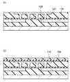
以下、本発明の第1の実施形態について、図1を参照して説明する。図1は本実施形態にかかる半導体装置の模式的断面図である。
半導体基板101上に絶縁膜102が形成され、絶縁膜102の上面の一部に配線溝120が形成され、その配線溝120にはたとえばCuからなる第1の導電層103および第2の導電層104が所定の距離を離間して形成されている。第1の導電層103および第2の導電層104を被覆するように拡散防止膜105が形成され、拡散防止膜105の上面にアリルエーテル系樹脂のようなヤング率の低い絶縁膜106が形成されている。絶縁膜106の上面には配線溝125が形成され、その配線溝125にはたとえばCuからなる第3の導電層108が形成され、第3の導電膜108が形成された絶縁膜106の上面には拡散防止膜109および絶縁膜110が形成されている。また、絶縁膜106には、第1の導電層103および第2の導電層104のいずれかがそれぞれ露出するような複数の第1の開口部107が形成され、第3の導電層108と第1の導電層103および第2の導電層104は、第1の開口部107を介して電気的に接続されている。さらに、2つの第1の開口部107の間に第3の導電層108に沿って、第1の導電層103および第2の導電層104のいずれもが露出されない第2の開口部111が所定の間隔L1 を隔てて形成されている。ここで、第1の開口部107および第2の開口部111は第3の導電層と同じ材料で埋め込まれている。なお、説明を簡単にするために、半導体基板に形成された素子領域や素子分離領域などの構成は図示を省略している。
【0019】
次に、本発明の半導体装置の製造方法について、図2〜6を参照して説明する。図2〜6は、本実施形態にかかる半導体装置の製造方法の主要な工程を順次模式的に示した概略断面図である。
図2(a)に示すように、所定の素子領域が形成された半導体基板101の上面に絶縁膜102を形成する。絶縁膜102の上面において、導電層形成領域に既存のリソグラフィー技術およびエッチング技術などを用いて、深さt1 の配線溝120を所定の距離離間してたとえば2ヵ所形成する。本実施形態においてはt1 は200nm程度とする。また、絶縁層102は、たとえば、アリルエーテル系樹脂の膜とする。
次に、図2(b)に示すように、配線溝120が形成された絶縁膜102の上面にバリアメタル121を形成し、その後、バリアメタルの上面に第1の金属層122を形成する。バリアメタルとして、たとえば、スパッタリング法などによりTa膜を10nm程度形成する。また、第1の金属層122として、Cuシード膜を80nm程度形成し、電界メッキ法などによりCuメッキ層700nm程度形成する。
【0020】
次に、図3(c)に示すように、化学機械的研磨(CMP:Chemical−Mechanical Polishing)技術などにより、第1の金属層122を絶縁膜102が露出するまで研磨し、配線溝120に第1の導電層103および第2の導電層104を形成する。本実施形態において、第1の導電層103と第2の導電層104とは、同一の金属層122から形成されたが、異なる金属層から形成してもよい。なお、図3(c)以降の工程においてはバリアメタルの図示を省略している。
次に、図3(d)に示すように、Cuの拡散を防止する拡散防止膜105としてSiC膜を50nm程度形成し、アリルエーテル系樹脂などのSiO2 膜などと比べてヤング率の低い絶縁膜106を600nm程度形成する。拡散防止膜105および絶縁膜106の形成方法は形成する材料によって所定の方法で行う。
【0021】
次に、図4(e)に示すように、絶縁膜106において、第1の導電層103および第2の導電層104のそれぞれの端部にそれぞれ第1の開口部107を既存のリソグラフィー技術およびエッチング技術を用いて形成する。同時に、2つの第1の開口部107の間に、第1の導電層103および第2の導電層104が形成された領域を除く第3の導電層108の形成領域に沿って第2の開口部111を所定の間隔L1 を隔てて形成する。このとき、第1の開口部107および第2の開口部111の底部には、拡散防止膜が残存していることが望ましい。
第2の開口部111を形成する間隔L1 は、後に形成する第3の導電層108の配線長、第3の導電層108および絶縁膜106のヤング率および熱膨張係数、後工程の加熱温度などに応じて決定される。ここでは、第3の導電層108の配線長において、100μm毎に形成する。
次に、図4(f)に示すように、絶縁膜106の上面に埋め込み層123を第1の開口部107および第2の開口部111を埋め込むように形成する。埋め込み層123の上面にレジスト膜124を形成し、既存のリソグラフィー技術を用いて第3の導電層108形成領域の所定のパターンにレジスト膜124を加工する。
【0022】
次に、図5(g)に示すように、既存のエッチング技術によりレジスト膜124が形成された領域を除く埋め込み層123および絶縁膜106を加工する。レジスト膜124および埋め込み層123を除去し、深さt2 の配線溝125を形成する。さらに、第1の開口部107および第2の開口部111において露出されている拡散防止膜105をエッチング技術などにより除去し、第1の開口部107において第1の導電層103および第2の導電層104を露出させ、第2の開口部111において、下層の絶縁層102を露出させる。このとき、配線溝125の深さt2 は、たとえば、300nmになるように加工する。
次に、図5(h)に示すように、第1の開口部107、第2の開口部111および配線溝125が形成された絶縁膜106の上面に、バリアメタル126および第2の金属層127を形成する。バリアメタル126として、たとえば、Ta膜をスパッタリング法などにより20nm程度形成する。また、第2の金属層127として、たとえば、スパッタリング法などによりCuシード膜を80nm程度形成し、Cu膜を電界メッキ法などにより800nm程度形成する。
【0023】
次に、図6(i)に示すように、CMP技術などにより絶縁膜106が露出するまで研磨し、配線溝125にのみバリアメタル126および第2の金属層127から形成される第3の導電層108を形成する。第3の導電層108は、上記材料に限らず、銅を含有する導電性材料であれば良い。図6(i)以降の工程においてはバリアメタル126の図示を省略する。
次に、図6(j)に示すように、以下同様の工程で拡散防止膜109および絶縁膜110を形成し、さらに必要に応じて導電層などを形成し、多層配線を形成する。
なお、第2の開口部111を形成する間隔L1 およびその数は、上記例に限定されず、導電層の膜厚あるいは開口部の寸法、絶縁膜の種類および膜厚などによって変化する。また、配線溝120,125の深さt1 t2 は、絶縁膜の種類および膜厚などにより変えることができる。
【0024】
本実施形態において、第3の導電層108に形成された2つの第1の開口部107の間に、100μmごとの間隔で第2の開口部111を形成し、絶縁膜106としてアリルエーテル系樹脂を用いる。そして、上層(第3の導電層108)および下層(第1および第2の導電層103,104)の導電層はCuを用い、第3の導電層108の両端において第1の開口部107により下層配線103,104と接続する。このとき、Cuは、ヤング率115Gpa、熱膨張率17.7ppm/℃であり、アリルエーテル系樹脂は、ヤング率2.45Gpa、熱膨張率66ppm/℃とする。
導電層103,104,108が、たとえば、1000μm(1000μmの上層導電層108と1000μmの下層導電層103,104の繰り返しの構造)程度の配線長に形成され、上層導電層と下層導電層との間にアリルエーテル系樹脂の絶縁膜106を形成されているとする。実際に使用する温度を100度程度とすると、上記のヤング率および熱膨張率から、導電層の端部は片側で約800nm程度も配線長が伸びることになる。つまり、開口部107においては、下層導電層103,104から一方に800nm程度、同様に上層導電層108から反対方向に800nm程度もの変形する力が加わる。
【0025】
130nm世代で考えると、開口部107,111の孔径は200nm程度であるのでその400%程度も配線長方向に変化させるだけの力が、上層および下層の導電層からおのおの反対方向に加わる。従って、第1の開口部107の底部とその真下の導電層103,104とはバリアメタルなどを介して接続しており、密着性が十分でないことから、導通不良になることが容易に考えられる。
そこで、たとえば、第3の導電層108の100μmごとに開口部107,111を形成した場合、導電層103,104,108の端部の片側においてそれぞれ80nm程度(孔径の40%)を変化させるだけの力となる。そのため、第2の開口部111が全くない場合の1/10の力となる。孔径の40%程度の変形であれば第1の開口部107において接続が保たれる可能性もある。本実施形態においては、10%オーダーの100μm程度が限界と考えられ、それ以下になるような間隔L1で第2の開口部111を形成する。
従来の方法のように、第2の開口部111を形成しないと、第3の導電層108の配線長の変化により接続部の変形しようとする力が、第1の開口部107における接続部にすべて加わる。しかし、電気的な接続に寄与しない第2の開口部111を第3の導電層108に沿って、複数の第1の開口部107の間に形成することにより、配線長の変形に伴い第1の開口部107に付与される力が分散する。
第1の開口部107および第2の開口部111を形成する所定の距離L1 は、本実施形態に限定されず、導電層の種類および膜厚、開口部の孔径、絶縁膜の種類および膜厚により変化する。
【0026】
本実施形態において、第1および第2の導電層と第3の導電層とが、第1の開口部により電気的に接続され、第3の導電層に沿って複数の第1の開口部の間に所定の間隔を隔てて導電層の接続に寄与しない第2の開口部を形成する。それにより、後工程の熱膨張あるいは収縮による第3の導電層の長手方向における配線長の変化に伴う力を分散し、第1の開口部の変形を抑制する。したがって、導電層の接続部である第3の導電層の両端部に形成された第1の開口部の底界面の剥がれを防止することができる。そのため、製品歩留りや配線信頼度が向上する。
【0027】
〔第2の実施形態〕
以下、本発明の第2の実施形態にかかる半導体装置の製造方法について図を参照して説明する。第1の実施形態と同様の部分は番号を同じくし、説明を省略し、以下、異なる部分についてのみ説明する。
図7は、本実施形態にかかる半導体装置を模式的に示した断面図である。
半導体基板101上に絶縁膜102が形成され、絶縁膜102の上面の一部に所定の距離が離間されて複数の配線溝120が形成され、その配線溝120にはそれぞれ第1の導電層103および第2の導電層104が所定の距離を離間して交互に形成されている。第1の導電層103および第2の導電層104はたとえばCuにより形成されている。第1の導電層103および第2の導電層104を被覆するように拡散防止膜105が形成され、拡散防止膜105の上面にアリルエーテル系樹脂のような低ヤング率の絶縁膜106が形成されている。絶縁膜106の上面には配線溝125が形成され、その配線溝125には所定の配線長L2 で第3の導電層108が形成され、第3の導電膜108が形成された絶縁膜106の上面には拡散防止膜109および絶縁膜110が形成されている。ここで、第3の導電層108はたとえばCuにより形成されている。また、所定の配線長L2 を有する第3の導電層108は、一方の端部において第1の導電層103と、他方の端部において第2の導電層104と、開口部112を介して電気的に接続されている。ここで、開口部112は第3の導電層108と同じ材料で埋め込まれている。なお、説明を簡単にするために、半導体基板に形成された素子領域や素子分離領域などの構成は図示を省略している。
【0028】
次に、本発明の半導体装置の製造方法について、図8、9を参照して説明する。図8、9は、本実施形態にかかる半導体装置の製造方法の主要な工程を順次模式的に示した概略断面図である。
図8(a)に示すように、上記と同様な方法で、所定の素子領域が形成された半導体基板101の上面に絶縁膜102を形成する。絶縁層102の上面において、導電層形成領域に既存のリソグラフィー技術およびエッチング技術などを用いて、所定の距離を離間して200nm程度の深さを有する配線溝120を複数形成する。配線溝120が形成された絶縁膜102の上面にバリアメタルとしてTa膜10nmを形成し、バリアメタル121の上面に第1の金属層としてCuシード膜80nm、およびCu膜700nmを形成する。
次に、CMP技術などにより、第1の金属層を絶縁膜102が露出するまで研磨し、配線溝120に第1の導電層103および第2の導電層104を形成する。本実施形態において、第1の導電層103と第2の導電層104とは、同一の金属層から形成されたが、異なる金属層から形成してもよい。なお、図中において、バリアメタルは図示を省略し、第1の金属層を第1の導電層103および第2の導電層104と示している。
【0029】
次に、図8(b)に示すように、第1の導電層103および第2の導電層104の拡散を防止する拡散防止膜105としてSiC膜50nmを形成し、アリルエーテル系樹脂などの低ヤング率の絶縁膜106を600nm程度形成する。拡散防止膜105および絶縁膜106の形成方法は用いる材料によって所定の方法で行う。また、拡散防止膜105は、導電層103,104の材料によって形成しなくてもよい。
次に、絶縁膜106において、第1の導電層103および第2の導電層104のそれぞれの端部に開口部112を、既存のリソグラフィー技術およびエッチング技術を用いて形成する。このとき、開口部112の底部において、拡散防止膜が残存していることが望ましい。
【0030】
次に、図9(c)に示すように、開口部112を埋め込むように、絶縁膜106の上面に埋め込み層を形成し、埋め込み層の上面にレジスト膜を形成し、既存のリソグラフィー技術を用いて第3の導電層108用の配線溝125領域を露出するように所定のパターンにレジスト膜を加工する。図中において、埋め込み層およびレジスト膜は図示を省略する。
次に、既存のエッチング技術により、レジスト膜が形成された領域を除く埋め込み層および絶縁膜106を加工する。そして、レジスト膜および埋め込み層を除去し、所定の長さL2 となる配線溝125を300nm程度の深さに形成する。さらに、開口部112において露出されている拡散防止膜105をエッチング技術などにより除去し、第1の導電層103および第2の導電層104を露出させる。
【0031】
次に、図9(d)に示すように、開口部112および配線溝125が形成された絶縁膜106の上面に、バリアメタルとしてTa膜20nm程度形成し、第2の金属層としてCuシード膜80nm、およびCu膜800nmを形成する。
CMP技術などにより絶縁膜106が露出するまで研磨し、配線溝125に所定の配線長L2 を有する第3の導電層108を形成する。第3の導電層108は、上記材料に限らず、Cuを含む導電性材料であれば良い。図中において、バリアメタルは省略し、第2の金属層を第3の導電層108を示している。
次に、上記と同様の工程で、拡散防止膜109および絶縁膜110を形成し、さらに必要に応じて導電層などを形成し、図7に示すような多層配線を形成する。
【0032】
図7に示すように、本実施形態において、第3の導電層108を所定の配線長L2 とし、たとえば、第3の導電層108の配線長を100μm程度に形成する。第3の導電層108の両端に形成された2つの開口部112により、一方の開口部112において第1の配線層103と、他方の開口部112において第2の配線層104とそれぞれ電気的に接続されている。また、第1の配線層103はその両端において、それぞれ異なる第3の導電層108と電気的に接続され、第2の導電層104は、その両端において、それぞれ異なる第3の導電層108と電気的に接続されている。このような構造が繰り返し形成されている。さらに、絶縁膜106としてアリルエーテル系樹脂を用い、開口部112は絶縁膜106に形成され、Cuにより形成された第3の導電層108と、下層の第1および第2の導電層103,104とを接続している。このとき、Cuは、ヤング率115Gpa,熱膨張率17.7ppm/℃であり、アリルエーテル系樹脂は、ヤング率2.45Gpa,熱膨張率66ppm/℃とする。
導電層103,104,108の配線長L2がたとえば、1000μm(1000μmの上層導電層と1000μm下層導電層の繰り返しの構造)程度に形成され、上層導電層と下層導電層との間にアリルエーテル系樹脂の絶縁膜106が形成されているとする。実際に使用する温度を100度程度とすると、上記ヤング率および熱膨張率から、導電層の端部は、片側でそれぞれ約800nm程度も伸びることになる。つまり、開口部112においては、下層導電層103,104から一方に800nm、上層導電層108から反対方向に800nm程度もの変形する力が加わる。
【0033】
130nm世代で考えると、開口部112の孔径は200nm程度であるのでその400%程度も配線長方向に変化させるだけの力が、上層および下層の導電層からおのおの反対方向に加わる。従って、開口部112の底部とその真下の導電層103,104とはバリアメタルなどを介して接続しており、密着性が十分でないことから、導通不良になることが容易に考えられる。
そこで、たとえば、第3の導電層108の配線長L2を100μmとした場合、導電層の端部において片側80nm程度(孔径の40%)を変化させるだけの力となるので、配線長L2が1000μmの場合に比べ、1/10程度の力に低減される。孔径の40%程度の変形であれば開口部112において接続が保たれる可能性もあり、本実施形態においては10%オーダーの100μm程度が限界であり、それ以下になるように第3の導電層108の配線長L2を形成する。
従来の方法のように、1本の長い導電層の両端において開口部により電気的な接続をしていると、導電層の膨張により接続部が変化しようとする力が開口部にすべて加わり、接続部が剥がれる可能性がある。しかし、第3の導電層108を導電層の熱膨張または収縮により長手方向の長さが変化しても開口部による接続が保たれるような所定の配線長L2 に形成することにより、配線長の膨張あるいは収縮に伴う開口部にかかる力が低減される。
【0034】
第3の導電層108の所定の配線長L2 は、本実施形態に限定されず、導電層の種類、膜厚、開口部の孔径、絶縁膜の種類および膜厚により変化する。また、第1の導電層103および第2の導電層104が、本実施形態のように第3の導電層108と同じ材料を用いて形成されている場合、第3の導電層108の配線長L2 と同程度の配線長に形成することが望ましい。さらに、第1の導電層103および第2の導電層104のそれぞれの導電層を形成する材料のヤング率および熱膨張率から上記と同様な方法で配線長を求めると、下層の電極から加わる力はより低減される。
【0035】
本実施形態において、第3の導電層の配線長を所定の長さにすることにより、熱膨張あるいは収縮により長手方向の配線長が変化しても、接続部における剥がれなどを抑制し、開口部の変形を防ぎ、接続を保つことができる。したがって、製品歩留りや配線信頼度が向上する。
【0036】
本発明は、上記の実施形態に限定されない。
たとえば、第1の実施形態においては、第1の開口部の間に形成された第2の開口部の間隔は、形成する導電層の膜厚、開口部の孔径などによって変更でき、また、第2の実施形態において第3の導電層の配線長は、導電層の膜厚や絶縁膜の種類によって変更できる。
その他、本発明の要旨を逸脱しない範囲で種々の変更が可能である。
【0037】
【発明の効果】
以上説明してきたように、本発明によれば、半導体装置において、導電層の熱膨張あるいは収縮による開口部の変形を抑制し、製品歩留りおよび配線信頼性を向上することができる。
また、半導体装置の製造方法において、導電層の熱膨張あるいは収縮による開口部の変形を抑制し、製品歩留りおよび配線信頼性を向上することができる。
【図面の簡単な説明】
【図1】図1は本発明の第1の実施形態にかかる半導体装置の一部を模式的に示す概略断面図である。
【図2】図2(a)は、本発明の第1の実施形態にかかる半導体装置の製造方法の主要な工程を順次模式的に示す概略断面図であり、図2(b)は、本発明の第1の実施形態にかかる半導体装置の製造方法の主要な工程を順次模式的に示す概略断面図である。
【図3】図3(c)は、本発明の第1の実施形態にかかる半導体装置の製造方法の主要な工程を順次模式的に示す概略断面図であり、図3(d)は、本発明の第1の実施形態にかかる半導体装置の製造方法の主要な工程を順次模式的に示す概略断面図である。
【図4】図4(e)は、本発明の第1の実施形態にかかる半導体装置の製造方法の主要な工程を順次模式的に示す概略断面図であり、図4(f)は、本発明の第1の実施形態にかかる半導体装置の製造方法の主要な工程を順次模式的に示す概略断面図である。
【図5】図5(g)は、本発明の第1の実施形態にかかる半導体装置の製造方法の主要な工程を順次模式的に示す概略断面図であり、図5(h)は、本発明の第1の実施形態にかかる半導体装置の製造方法の主要な工程を順次模式的に示す概略断面図である。
【図6】図6(i)は、本発明の第1の実施形態にかかる半導体装置の製造方法の主要な工程を順次模式的に示す概略断面図であり、図6(j)は、本発明の第1の実施形態にかかる半導体装置の製造方法の主要な工程を順次模式的に示す概略断面図である。
【図7】図7は本発明の第2の実施形態にかかる半導体装置の一部を模式的に示す概略断面図である。
【図8】図8(a)は、本発明の第2の実施形態にかかる半導体装置の製造方法の主要な工程を順次模式的に示す概略断面図であり、図8(b)は、本発明の第2の実施形態にかかる半導体装置の製造方法の主要な工程を順次模式的に示す概略断面図である。
【図9】図9(c)は、本発明の第2の実施形態にかかる半導体装置の製造方法の主要な工程を順次模式的に示す概略断面図であり、図9(d)は、本発明の第2の実施形態にかかる半導体装置の製造方法の主要な工程を順次模式的に示す概略断面図である。
【図10】図10は従来の技術にかかる半導体装置の一部を模式的に示す概略断面図である。
【図11】図11は従来の技術にかかる半導体装置の一部を模式的に示す概略断面図である。
【符号の説明】
1…基板、2…絶縁膜、3…第1の導電層、4…第2の導電層、5…拡散防止膜、6…絶縁膜、7…開口部、8…第3の導電層、9…拡散防止膜、10…絶縁膜、20…導電層、101…基板、102…絶縁膜、103…第1の導電層、104…第2の導電層、105…拡散防止膜、106…絶縁膜、107…第1の開口部、108…第3の導電層、109…拡散防止膜、110…絶縁膜、111…第2の開口部、112…開口部、120…配線溝、121…バリアメタル、122…第1の金属層、123…埋め込み層、124…レジスト膜、125…配線溝、126…バリアメタル、127…第2の金属層[0001]
BACKGROUND OF THE INVENTION
The present invention relates to a semiconductor device and a method for manufacturing the same, and more particularly to a semiconductor device having a multilayer wiring that electrically connects a plurality of conductive layers through connection holes formed in an insulating film and a method for manufacturing the same.
[0002]
[Prior art]
Along with higher integration and higher performance of LSIs, device dimensions have been miniaturized and multilayer structures have been advanced. In order to reduce the wiring delay that increases due to the miniaturization of multilayer wiring, parameters that affect wiring resistance and capacitance (wiring film thickness), parameters that affect wiring capacitance (interlayer film thickness, relative dielectric constant), and wiring It is necessary to scale parameters (wiring resistivity) that affect the resistance at an appropriate ratio.
[0003]
As a wiring material, it is desirable that the resistivity is low in order to propagate an electric signal without a large voltage drop. Au, Cu, Ag, etc. are mentioned as those having a low resistivity with respect to Al that has been widely used. Among these, Cu has a higher melting point than Al, and it has been reported that reliability is improved as compared with Al because of the high activation energy of the electromigration phenomenon. However, in order to use Cu for fine wiring, in the dry etching method, since there is no suitable gas for etching Cu with a high selection ratio with respect to the underlying insulating film, a buried wiring forming technique [ A buried wiring is formed by a damascene method. In particular, a dual damascene method in which the connection hole and the wiring are simultaneously embedded is useful from the viewpoint of increasing the alignment margin and shortening the process in lithography.
[0004]
Further, as the insulating film, a film having a small relative dielectric constant is desirable from the viewpoint of reducing the wiring capacitance. The materials used have shifted to low dielectric constant materials typified by allyl ether resins and SiOC. However, low-dielectric constant materials such as allyl ether resins are conventionally used
[0005]
FIG. 10 is a schematic cross-sectional view schematically showing a part of a conventional semiconductor device. An
[0006]
As a conventional method for manufacturing a semiconductor device as described above, the interlayer insulating film formed on the substrate, the upper layer wiring and the lower layer wiring formed on the substrate, and the upper layer wiring and the lower layer wiring are electrically connected. It is known to form a plug and to form a column that does not serve as a current flow path in an interlayer insulating film near the plug (see, for example, Patent Document 1).
[0007]
[Patent Document 1]
Japanese Patent Laid-Open No. 11-154679 (page 3-7, FIG. 1-10)
[0008]
[Problems to be solved by the invention]
However, in the conventional method as described above, an insulating film having a low Young's modulus is used, so that the longitudinal direction of the conductive layer expands and contracts due to thermal expansion or contraction of the conductive layer in a high temperature atmosphere during the process. Easily deform.
FIG. 11 shows an example of the deformation of the wiring and connection portion in a high temperature atmosphere (for example, about 400 ° C.).
FIG. 11 is a schematic cross-sectional view schematically showing a part of a semiconductor device according to the prior art, and shows a state of wiring at a high temperature in the configuration of FIG.
10 and 11, when one long third
In this way, the connection portion between particularly fragile wires is deformed to cause a disconnection or the like, so that it may have a great influence on product yield and wiring reliability.
[0009]
The present invention has been made in view of such circumstances, and an object thereof is to suppress deformation of an opening due to thermal expansion or contraction of a conductive layer, and to improve a product yield and wiring reliability, and a manufacturing method thereof. Is to provide.
[0010]
[Means for Solving the Problems]
In order to achieve the above object, a semiconductor device according to the present invention is formed on a substrate, a first conductive layer formed on the substrate, and a predetermined distance from the first conductive layer. Formed on the top surfaces of the second conductive layer, the first conductive layer, and the second conductive layer so that either the first conductive layer or the second conductive layer is exposed. A plurality of first openings formed, and a second opening formed so that neither the first conductive layer nor the second conductive layer is exposed.And SiO2Membrane and fluorine-containing SiO2Lower Young's modulus than membraneAn insulating film is formed on an upper surface of the insulating film so as to embed the first opening and the second opening, and the first conductive layer and the second opening are formed via the first opening. A third conductive layer electrically connected to the conductive layer, and the second opening is formed between the two first openings along the third conductive layer. Yes.
[0011]
In the semiconductor device of the present invention, the second opening is formed between the two first openings along the third conductive layer, thereby dispersing the force applied to the first opening. Then, deformation of the first opening, which is a connection portion between one of the first conductive layer and the second conductive layer, and the third conductive layer is suppressed.
[0012]
The semiconductor device according to the present invention includes a substrate, a first conductive layer formed on the substrate, and a second conductive layer formed on the substrate at a predetermined distance from the first conductive layer. And openings formed on the top surfaces of the first conductive layer and the second conductive layer so that either end of the first conductive layer and the second conductive layer is exposed. Have partAnd SiO2Membrane and fluorine-containing SiO2Lower Young's modulus than membraneAn insulating film, and a third conductive layer formed on the upper surface of the insulating film so as to fill the opening, and electrically connected to the first conductive layer and the second conductive layer; The third conductive layer has a predetermined wiring length so that the connection is maintained even if the length in the longitudinal direction changes due to thermal expansion or contraction, and the third conductive layer has the first conductive layer at both ends of the third conductive layer. The first conductive layer and the second conductive layer are electrically connected through the opening.
[0013]
In the semiconductor device according to the present invention, the first conductive layer and the second conductive layer have the predetermined wiring length so that the first conductive layer and the second conductive layer can be formed even if the length in the longitudinal direction changes due to thermal expansion or contraction. Electrical connection is maintained through the conductive layer and the opening.
[0014]
The method for manufacturing a semiconductor device of the present invention includes a step of forming a first conductive layer on a substrate, and a step of forming a second conductive layer on the substrate at a predetermined distance from the first conductive layer. , On top surfaces of the first conductive layer and the second conductive layerSiO2Membrane and fluorine-containing SiO2Lower Young's modulus than membraneA step of forming an insulating film, a plurality of first openings that expose either the first conductive layer or the second conductive layer in the insulating film, and the first conductive layer And forming a second opening that does not expose any of the second conductive layer, filling the first opening and the second opening, and via the first opening Forming a third conductive layer on the upper surface of the insulating film so as to be electrically connected to the first conductive layer and the second conductive layer, and the second opening includes Formed between the two first openings along the third conductive layer.
[0015]
In the semiconductor device manufacturing method of the present invention, the first conductive layer is formed on the substrate, and the second conductive layer is formed on the substrate at a predetermined distance from the first conductive layer. A plurality of first openings in which an insulating film is formed on the top surfaces of the first conductive layer and the second conductive layer, and any one of the first conductive layer and the second conductive layer is exposed in the insulating film. And a second opening so that neither the first conductive layer nor the second conductive layer is exposed. The third opening is embedded in the upper surface of the insulating film so as to be embedded in the first opening and the second opening and to be electrically connected to the first conductive layer and the second conductive layer through the first opening. Form a layer. Here, the second opening is formed between the two first openings along the third conductive layer.
[0016]
The method for manufacturing a semiconductor device of the present invention includes a step of forming a first conductive layer on a substrate, and a step of forming a second conductive layer on the substrate at a predetermined distance from the first conductive layer. , On top surfaces of the first conductive layer and the second conductive layerSiO2Membrane and fluorine-containing SiO2Lower Young's modulus than membraneForming an insulating film; forming an opening such that one end of each of the first conductive layer and the second conductive layer is exposed in the insulating film; and embedding the opening. Forming a third conductive layer on the upper surface of the insulating film so as to be electrically connected to the first conductive layer and the second conductive layer, and wiring for the third conductive layer The length is formed to a predetermined length so that the connection is maintained even if the length in the longitudinal direction changes due to thermal expansion or contraction, and the first conductive layer and the second conductive layer are formed at both ends of the third conductive layer. The second conductive layer is formed so as to be electrically connected through the opening.
[0017]
In the semiconductor device manufacturing method of the present invention, the first conductive layer is formed on the substrate, and the second conductive layer is formed on the substrate at a predetermined distance from the first conductive layer. An insulating film is formed on the top surfaces of the first conductive layer and the second conductive layer, and an opening is formed in the insulating film so that one end of each of the first conductive layer and the second conductive layer is exposed. To do. A third conductive layer is formed on the upper surface of the insulating film so as to fill the opening and to be electrically connected to the first conductive layer and the second conductive layer. Here, the wiring length of the third conductive layer is formed to a predetermined length so that the connection is maintained even if the length in the longitudinal direction changes due to thermal expansion or contraction, and both ends of the third conductive layer are formed. The first conductive layer and the second conductive layer are electrically connected to each other through the opening.
[0018]
DETAILED DESCRIPTION OF THE INVENTION
Hereinafter, embodiments of the present invention will be described with reference to the drawings.
[First Embodiment]
Hereinafter, a first embodiment of the present invention will be described with reference to FIG. FIG. 1 is a schematic cross-sectional view of a semiconductor device according to this embodiment.
An insulating
[0019]
Next, the manufacturing method of the semiconductor device of this invention is demonstrated with reference to FIGS. 2 to 6 are schematic cross-sectional views sequentially illustrating main steps of the method for manufacturing the semiconductor device according to this embodiment.
As shown in FIG. 2A, an insulating
Next, as shown in FIG. 2B, a
[0020]
Next, as shown in FIG. 3C, the
Next, as shown in FIG. 3D, an SiC film is formed to a thickness of about 50 nm as the
[0021]
Next, as shown in FIG. 4E, in the insulating
Interval L for forming the
Next, as shown in FIG. 4F, a buried
[0022]
Next, as shown in FIG. 5G, the buried
Next, as shown in FIG. 5H, the
[0023]
Next, as shown in FIG. 6I, the third conductive layer is polished by the CMP technique or the like until the insulating
Next, as shown in FIG. 6J, a
Note that the interval L at which the
[0024]
In the present embodiment, the
The
[0025]
Considering the 130 nm generation, since the
Therefore, for example, when the
If the
A predetermined distance L for forming the
[0026]
In the present embodiment, the first and second conductive layers and the third conductive layer are electrically connected through the first opening, and a plurality of first openings are formed along the third conductive layer. A second opening that does not contribute to the connection of the conductive layer is formed with a predetermined gap therebetween. Thereby, the force accompanying the change in the wiring length in the longitudinal direction of the third conductive layer due to the thermal expansion or contraction in the subsequent process is dispersed, and the deformation of the first opening is suppressed. Therefore, it is possible to prevent peeling of the bottom interface of the first opening formed at both ends of the third conductive layer which is a connection portion of the conductive layer. Therefore, product yield and wiring reliability are improved.
[0027]
[Second Embodiment]
A method for manufacturing a semiconductor device according to the second embodiment of the present invention will be described below with reference to the drawings. The same parts as those of the first embodiment are denoted by the same reference numerals, description thereof is omitted, and only different parts will be described below.
FIG. 7 is a cross-sectional view schematically showing the semiconductor device according to the present embodiment.
An insulating
[0028]
Next, a method for manufacturing a semiconductor device of the present invention will be described with reference to FIGS. 8 and 9 are schematic cross-sectional views schematically sequentially showing main processes of the method for manufacturing a semiconductor device according to the present embodiment.
As shown in FIG. 8A, an insulating
Next, the first metal layer is polished by CMP technique or the like until the insulating
[0029]
Next, as shown in FIG. 8B, an SiC film 50 nm is formed as a
Next, in the insulating
[0030]
Next, as shown in FIG. 9C, a buried layer is formed on the upper surface of the insulating
Next, the buried layer and the insulating
[0031]
Next, as shown in FIG. 9D, a Ta film of about 20 nm is formed as a barrier metal on the upper surface of the insulating
Polishing is performed by the CMP technique or the like until the insulating
Next, in the same process as described above, the
[0032]
As shown in FIG. 7, in the present embodiment, the third
Wiring length L of
[0033]
Considering the 130 nm generation, since the hole diameter of the
Therefore, for example, the wiring length L of the third
As in the conventional method, when the electrical connection is made by the opening at both ends of one long conductive layer, all the force to change the connection due to the expansion of the conductive layer is applied to the opening, and the connection is made. Part may be peeled off. However, the third
[0034]
A predetermined wiring length L of the third
[0035]
In this embodiment, by setting the wiring length of the third conductive layer to a predetermined length, even if the wiring length in the longitudinal direction changes due to thermal expansion or contraction, peeling at the connection portion is suppressed, and the opening portion Can prevent the deformation and keep the connection. Therefore, product yield and wiring reliability are improved.
[0036]
The present invention is not limited to the above embodiment.
For example, in the first embodiment, the interval between the second openings formed between the first openings can be changed depending on the film thickness of the conductive layer to be formed, the hole diameter of the openings, etc. In the second embodiment, the wiring length of the third conductive layer can be changed depending on the thickness of the conductive layer and the type of the insulating film.
In addition, various modifications can be made without departing from the scope of the present invention.
[0037]
【The invention's effect】
As described above, according to the present invention, in the semiconductor device, the deformation of the opening due to the thermal expansion or contraction of the conductive layer can be suppressed, and the product yield and the wiring reliability can be improved.
In addition, in the method for manufacturing a semiconductor device, deformation of the opening due to thermal expansion or contraction of the conductive layer can be suppressed, and product yield and wiring reliability can be improved.
[Brief description of the drawings]
FIG. 1 is a schematic cross-sectional view schematically showing a part of a semiconductor device according to a first embodiment of the present invention.
2A is a schematic cross-sectional view schematically showing main steps of the method of manufacturing the semiconductor device according to the first embodiment of the present invention, and FIG. It is a schematic sectional drawing which shows typically the main process of the manufacturing method of the semiconductor device concerning the 1st Embodiment of the invention sequentially.
FIG. 3C is a schematic cross-sectional view sequentially showing main steps of the method for manufacturing the semiconductor device according to the first embodiment of the present invention, and FIG. It is a schematic sectional drawing which shows typically the main process of the manufacturing method of the semiconductor device concerning the 1st Embodiment of the invention sequentially.
FIG. 4E is a schematic cross-sectional view sequentially showing main steps of the method for manufacturing the semiconductor device according to the first embodiment of the present invention, and FIG. It is a schematic sectional drawing which shows typically the main process of the manufacturing method of the semiconductor device concerning the 1st Embodiment of the invention sequentially.
FIG. 5G is a schematic cross-sectional view sequentially showing main steps of the method for manufacturing the semiconductor device according to the first embodiment of the present invention, and FIG. It is a schematic sectional drawing which shows typically the main process of the manufacturing method of the semiconductor device concerning the 1st Embodiment of the invention sequentially.
FIG. 6 (i) is a schematic cross-sectional view schematically showing the main steps of the semiconductor device manufacturing method according to the first embodiment of the present invention in sequence, and FIG. It is a schematic sectional drawing which shows typically the main process of the manufacturing method of the semiconductor device concerning the 1st Embodiment of the invention sequentially.
FIG. 7 is a schematic cross-sectional view schematically showing a part of a semiconductor device according to a second embodiment of the present invention.
FIG. 8A is a schematic cross-sectional view schematically showing the main steps of a method for manufacturing a semiconductor device according to a second embodiment of the present invention, and FIG. It is a schematic sectional drawing which shows typically the main process of the manufacturing method of the semiconductor device concerning the 2nd Embodiment of invention one by one.
FIG. 9C is a schematic cross-sectional view sequentially showing main steps of the semiconductor device manufacturing method according to the second embodiment of the present invention, and FIG. It is a schematic sectional drawing which shows typically the main process of the manufacturing method of the semiconductor device concerning the 2nd Embodiment of invention one by one.
FIG. 10 is a schematic cross-sectional view schematically showing a part of a conventional semiconductor device.
FIG. 11 is a schematic cross-sectional view schematically showing a part of a conventional semiconductor device.
[Explanation of symbols]
DESCRIPTION OF
Claims (9)
Translated fromJapanese前記基板に形成された第1の導電層と、
前記第1の導電層と所定の距離を離間して前記基板に形成された第2の導電層と、
前記第1の導電層および前記第2の導電層の上面に形成され、前記第1の導電層および前記第2の導電層のいずれかがそれぞれ露出するように形成された複数の第1の開口部と、前記第1の導電層および前記第2の導電層のいずれもが露出しないように形成された第2の開口部とを有し、SiO2膜およびフッ素含有のSiO2膜よりもヤング率が低い絶縁膜と、
前記第1の開口部および前記第2の開口部を埋め込むように前記絶縁膜の上面に形成され、前記第1の開口部を介して前記第1の導電層および前記第2の導電層と電気的に接続された第3の導電層と
を有し、
前記第2の開口部は、前記第3の導電層に沿って2つの前記第1の開口部の間に形成されている
半導体装置。A substrate,
A first conductive layer formed on the substrate;
A second conductive layer formed on the substrate at a predetermined distance from the first conductive layer;
A plurality of first openings formed on the top surfaces of the first conductive layer and the second conductive layer so as to expose either the first conductive layer or the second conductive layer.possess a part, and a second opening both of the first conductive layer and the second conductive layer is formed so as not to beexposed, SiO2Film and fluorine-containing SiO2An insulating film having aYoung's modulus lower than that of the film;
Formed on the upper surface of the insulating film so as to embed the first opening and the second opening, and the first conductive layer and the second conductive layer are electrically connected via the first opening. A third conductive layer connected electrically,
The second opening is formed between the two first openings along the third conductive layer. Semiconductor device.
請求項1記載の半導体装置。The semiconductor device according to claim 1, wherein the second opening is formed with a predetermined interval between the first openings.
請求項1記載の半導体装置。The semiconductor device according to claim 1, wherein the third conductive layer is formed of a conductive material containing copper.
前記基板に形成された第1の導電層と、
前記第1の導電層と所定の距離を離間して前記基板に形成された第2の導電層と、
前記第1の導電層および前記第2の導電層の上面に形成され、前記第1の導電層および前記第2の導電層のいずれかの端部がそれぞれ露出するように形成された開口部を有し、SiO2膜およびフッ素含有のSiO2膜よりもヤング率が低い絶縁膜と、
前記開口部を埋め込むように前記絶縁膜の上面に形成され、前記第1の導電層および前記第2の導電層と電気的に接続された第3の導電層と
を有し、
前記第3の導電層は、熱膨張または収縮により長手方向の長さが変化しても接続が保たれるような所定の配線長を有し、前記第3の導電層の両端において、前記第1の導電層および前記第2の導電層と前記開口部を介して電気的に接続されている
半導体装置。A substrate,
A first conductive layer formed on the substrate;
A second conductive layer formed on the substrate at a predetermined distance from the first conductive layer;
An opening formed on an upper surface of the first conductive layer and the second conductive layer, and formed so as to expose one end of each of the first conductive layer and the second conductive layer; Yesand, SiO2Film and fluorine-containing SiO2An insulating film having aYoung's modulus lower than that of the film;
A third conductive layer formed on the upper surface of the insulating film so as to fill the opening, and electrically connected to the first conductive layer and the second conductive layer;
The third conductive layer has a predetermined wiring length so that the connection is maintained even if the length in the longitudinal direction changes due to thermal expansion or contraction, and the third conductive layer has the first conductive layer at both ends of the third conductive layer. A semiconductor device electrically connected to one conductive layer and the second conductive layer through the opening.
請求項4記載の半導体装置。The semiconductor device according to claim 4, wherein the third conductive layer is formed of a conductive material containing copper.
前記第1の導電層と所定の距離を離間して前記基板に第2の導電層を形成する工程と、
前記第1の導電層および前記第2の導電層の上面にSiO2膜およびフッ素含有のSiO2膜よりもヤング率が低い絶縁膜を形成する工程と、
前記絶縁膜に、前記第1の導電層および前記第2の導電層のいずれかがそれぞれ露出するような複数の第1の開口部と、前記第1の導電層および前記第2の導電層のいずれもが露出しないような第2の開口部とを形成する工程と、
前記第1の開口部および前記第2の開口部を埋め込み、前記開口部を介して前記第1の導電層および前記第2の導電層と電気的に接続するように前記絶縁膜の上面に第3の導電層を形成する工程と
を有し、
前記第2の開口部は、前記第3の導電層に沿って2つの前記第1の開口部の間に形成する
半導体装置の製造方法。Forming a first conductive layer on a substrate;
Forming a second conductive layer on the substrate at a predetermined distance from the first conductive layer;
SiO2 on the top surfaces of the first conductive layer and the second conductive layerFilm and fluorine-containing SiO2 Forming an insulating film having alower Young's modulus than the film;
A plurality of first openings such that any one of the first conductive layer and the second conductive layer is exposed in the insulating film, and the first conductive layer and the second conductive layer Forming a second opening so that none of them are exposed;
The first opening and the second opening are buried, and the first conductive layer and the second conductive layer are electrically connected to the first conductive layer and the second conductive layer through the opening. And 3 forming a conductive layer,
The method of manufacturing a semiconductor device, wherein the second opening is formed between the two first openings along the third conductive layer.
請求項6に記載の半導体装置の製造方法。A method for manufacturing a semiconductor device according to claim 6.
前記第1の導電層と所定の距離を離間して前記基板に第2の導電層を形成する工程と、Forming a second conductive layer on the substrate at a predetermined distance from the first conductive layer;
前記第1の導電層および前記第2の導電層の上面にSiO SiO is formed on the top surfaces of the first conductive layer and the second conductive layer.22膜およびフッ素含有のSiOMembrane and fluorine-containing SiO22膜よりもヤング率が低い絶縁膜を形成する工程と、Forming an insulating film having a lower Young's modulus than the film;
前記絶縁膜に前記第1の導電層および前記第2の導電層のいずれかの端部がそれぞれ露出するように開口部を形成する工程と、Forming an opening in the insulating film such that one end of either the first conductive layer or the second conductive layer is exposed;
前記開口部を埋め込み、前記第1の導電層および前記第2の導電層と電気的に接続するように前記絶縁膜の上面に第3の導電層を形成する工程とForming a third conductive layer on an upper surface of the insulating film so as to fill the opening and to be electrically connected to the first conductive layer and the second conductive layer;
を有し、Have
前記第3の導電層の配線長は、熱膨張または収縮により長手方向の長さが変化しても接続が保たれるような所定の長さに形成し、前記第3の導電層の両端において、前記第1の導電層および前記第2の導電層と、前記開口部を介して電気的に接続するように形成するThe wiring length of the third conductive layer is formed to a predetermined length so that the connection is maintained even if the length in the longitudinal direction changes due to thermal expansion or contraction. The first conductive layer and the second conductive layer are electrically connected to each other through the opening.
半導体装置の製造方法。A method for manufacturing a semiconductor device.
請求項8に記載の半導体装置の製造方法。A method for manufacturing a semiconductor device according to claim 8.
Priority Applications (4)
| Application Number | Priority Date | Filing Date | Title |
|---|---|---|---|
| JP2003111437AJP3858849B2 (en) | 2003-04-16 | 2003-04-16 | Semiconductor device and manufacturing method thereof |
| US10/824,229US7279791B2 (en) | 2003-04-16 | 2004-04-14 | Semiconductor device and method of fabricating the same |
| KR1020040025724AKR20040090482A (en) | 2003-04-16 | 2004-04-14 | Semiconductor device and method of fabricating the same |
| TW093110569ATWI243426B (en) | 2003-04-16 | 2004-04-15 | Semiconductor device and method of fabricating the same |
Applications Claiming Priority (1)
| Application Number | Priority Date | Filing Date | Title |
|---|---|---|---|
| JP2003111437AJP3858849B2 (en) | 2003-04-16 | 2003-04-16 | Semiconductor device and manufacturing method thereof |
Publications (2)
| Publication Number | Publication Date |
|---|---|
| JP2004319745A JP2004319745A (en) | 2004-11-11 |
| JP3858849B2true JP3858849B2 (en) | 2006-12-20 |
Family
ID=33471988
Family Applications (1)
| Application Number | Title | Priority Date | Filing Date |
|---|---|---|---|
| JP2003111437AExpired - Fee RelatedJP3858849B2 (en) | 2003-04-16 | 2003-04-16 | Semiconductor device and manufacturing method thereof |
Country Status (4)
| Country | Link |
|---|---|
| US (1) | US7279791B2 (en) |
| JP (1) | JP3858849B2 (en) |
| KR (1) | KR20040090482A (en) |
| TW (1) | TWI243426B (en) |
Families Citing this family (7)
| Publication number | Priority date | Publication date | Assignee | Title |
|---|---|---|---|---|
| US7981789B2 (en) | 2008-11-14 | 2011-07-19 | Infineon Technologies Ag | Feature patterning methods and structures thereof |
| US9801277B1 (en) | 2013-08-27 | 2017-10-24 | Flextronics Ap, Llc | Bellows interconnect |
| US10466118B1 (en) | 2015-08-28 | 2019-11-05 | Multek Technologies, Ltd. | Stretchable flexible durable pressure sensor |
| CN108538799B (en)* | 2017-03-02 | 2024-02-27 | 弗莱克斯有限公司 | Interconnect component and interconnect assembly |
| US10426029B1 (en) | 2018-01-18 | 2019-09-24 | Flex Ltd. | Micro-pad array to thread flexible attachment |
| US10687421B1 (en) | 2018-04-04 | 2020-06-16 | Flex Ltd. | Fabric with woven wire braid |
| US10575381B1 (en) | 2018-06-01 | 2020-02-25 | Flex Ltd. | Electroluminescent display on smart textile and interconnect methods |
Family Cites Families (3)
| Publication number | Priority date | Publication date | Assignee | Title |
|---|---|---|---|---|
| JPH1056082A (en)* | 1996-08-07 | 1998-02-24 | Mitsubishi Electric Corp | Semiconductor integrated circuit device and method of manufacturing the same |
| US6495442B1 (en)* | 2000-10-18 | 2002-12-17 | Magic Corporation | Post passivation interconnection schemes on top of the IC chips |
| JP3790469B2 (en)* | 2001-12-21 | 2006-06-28 | 富士通株式会社 | Semiconductor device |
- 2003
- 2003-04-16JPJP2003111437Apatent/JP3858849B2/ennot_activeExpired - Fee Related
- 2004
- 2004-04-14USUS10/824,229patent/US7279791B2/ennot_activeExpired - Lifetime
- 2004-04-14KRKR1020040025724Apatent/KR20040090482A/ennot_activeWithdrawn
- 2004-04-15TWTW093110569Apatent/TWI243426B/ennot_activeIP Right Cessation
Also Published As
| Publication number | Publication date |
|---|---|
| TWI243426B (en) | 2005-11-11 |
| JP2004319745A (en) | 2004-11-11 |
| US20040256725A1 (en) | 2004-12-23 |
| KR20040090482A (en) | 2004-10-25 |
| US7279791B2 (en) | 2007-10-09 |
| TW200428530A (en) | 2004-12-16 |
Similar Documents
| Publication | Publication Date | Title |
|---|---|---|
| US11488862B2 (en) | Semiconductor device with reduced via resistance | |
| KR100385227B1 (en) | Semiconductor device having copper multy later circuit line and method of making the same | |
| JP3961412B2 (en) | Semiconductor device and method for forming the same | |
| KR0167812B1 (en) | Method of providing interconnection structure for semiconductor integrated chip | |
| JP3778487B2 (en) | Method for forming metal capacitor | |
| JPH11251316A (en) | Method for manufacturing multi-chip semiconductor device | |
| US7932187B2 (en) | Method for fabricating a semiconductor device | |
| TWI344685B (en) | An integrated circuit device and a process for forming the same | |
| JP3858849B2 (en) | Semiconductor device and manufacturing method thereof | |
| JPH10214891A (en) | Semiconductor device | |
| JPH11186391A (en) | Semiconductor device and manufacturing method thereof | |
| JP2002064140A (en) | Semiconductor device and method of manufacturing the same | |
| KR100640535B1 (en) | Multilayer copper interconnection structure of semiconductor device having dummy via contact and method of forming the same | |
| TW501233B (en) | Dual damascene process utilizing a low-k dual dielectric | |
| KR100588664B1 (en) | Copper diffusion preventing film formation method of semiconductor device | |
| KR100295141B1 (en) | Metal wiring layer formation method of semiconductor device | |
| KR100606537B1 (en) | Metal wiring formation method of semiconductor device using pullback process | |
| JP2008108892A (en) | Method for forming interconnection of semiconductor device, and interconnection | |
| JP2004140180A (en) | Semiconductor device and manufacturing method thereof | |
| KR20040057547A (en) | Method for forming copper wire in a semiconductor device | |
| KR19990006022A (en) | Metal wiring formation method of semiconductor device | |
| JP2004193422A (en) | Semiconductor device and manufacturing method thereof | |
| JPH05235172A (en) | Method for manufacturing semiconductor device |
Legal Events
| Date | Code | Title | Description |
|---|---|---|---|
| A621 | Written request for application examination | Free format text:JAPANESE INTERMEDIATE CODE: A621 Effective date:20040811 | |
| A977 | Report on retrieval | Free format text:JAPANESE INTERMEDIATE CODE: A971007 Effective date:20051116 | |
| A131 | Notification of reasons for refusal | Free format text:JAPANESE INTERMEDIATE CODE: A131 Effective date:20051122 | |
| A521 | Request for written amendment filed | Free format text:JAPANESE INTERMEDIATE CODE: A523 Effective date:20060120 | |
| TRDD | Decision of grant or rejection written | ||
| A01 | Written decision to grant a patent or to grant a registration (utility model) | Free format text:JAPANESE INTERMEDIATE CODE: A01 Effective date:20060829 | |
| A61 | First payment of annual fees (during grant procedure) | Free format text:JAPANESE INTERMEDIATE CODE: A61 Effective date:20060911 | |
| FPAY | Renewal fee payment (event date is renewal date of database) | Free format text:PAYMENT UNTIL: 20100929 Year of fee payment:4 | |
| FPAY | Renewal fee payment (event date is renewal date of database) | Free format text:PAYMENT UNTIL: 20100929 Year of fee payment:4 | |
| FPAY | Renewal fee payment (event date is renewal date of database) | Free format text:PAYMENT UNTIL: 20110929 Year of fee payment:5 | |
| FPAY | Renewal fee payment (event date is renewal date of database) | Free format text:PAYMENT UNTIL: 20110929 Year of fee payment:5 | |
| FPAY | Renewal fee payment (event date is renewal date of database) | Free format text:PAYMENT UNTIL: 20120929 Year of fee payment:6 | |
| FPAY | Renewal fee payment (event date is renewal date of database) | Free format text:PAYMENT UNTIL: 20120929 Year of fee payment:6 | |
| FPAY | Renewal fee payment (event date is renewal date of database) | Free format text:PAYMENT UNTIL: 20130929 Year of fee payment:7 | |
| R250 | Receipt of annual fees | Free format text:JAPANESE INTERMEDIATE CODE: R250 | |
| R250 | Receipt of annual fees | Free format text:JAPANESE INTERMEDIATE CODE: R250 | |
| R250 | Receipt of annual fees | Free format text:JAPANESE INTERMEDIATE CODE: R250 | |
| R250 | Receipt of annual fees | Free format text:JAPANESE INTERMEDIATE CODE: R250 | |
| R250 | Receipt of annual fees | Free format text:JAPANESE INTERMEDIATE CODE: R250 | |
| LAPS | Cancellation because of no payment of annual fees |