JP3855950B2 - Capacitive humidity sensor - Google Patents
Capacitive humidity sensorDownload PDFInfo
- Publication number
- JP3855950B2 JP3855950B2JP2003075017AJP2003075017AJP3855950B2JP 3855950 B2JP3855950 B2JP 3855950B2JP 2003075017 AJP2003075017 AJP 2003075017AJP 2003075017 AJP2003075017 AJP 2003075017AJP 3855950 B2JP3855950 B2JP 3855950B2
- Authority
- JP
- Japan
- Prior art keywords
- film
- moisture
- detection
- humidity
- electrodes
- Prior art date
- Legal status (The legal status is an assumption and is not a legal conclusion. Google has not performed a legal analysis and makes no representation as to the accuracy of the status listed.)
- Expired - Fee Related
Links
- 238000001514detection methodMethods0.000claimsdescription103
- 239000004065semiconductorSubstances0.000claimsdescription27
- 239000000758substrateSubstances0.000claimsdescription24
- 108010025899gelatin filmProteins0.000claimsdescription4
- 239000003990capacitorSubstances0.000description20
- 239000012528membraneSubstances0.000description13
- 238000004519manufacturing processMethods0.000description7
- 238000000034methodMethods0.000description7
- 239000004642PolyimideSubstances0.000description6
- XUIMIQQOPSSXEZ-UHFFFAOYSA-NSiliconChemical compound[Si]XUIMIQQOPSSXEZ-UHFFFAOYSA-N0.000description6
- 238000012937correctionMethods0.000description6
- 238000013461designMethods0.000description6
- 229920001721polyimidePolymers0.000description6
- 229910052710siliconInorganic materials0.000description6
- 239000010703siliconSubstances0.000description6
- 229910052581Si3N4Inorganic materials0.000description5
- 239000000463materialSubstances0.000description5
- HQVNEWCFYHHQES-UHFFFAOYSA-Nsilicon nitrideChemical compoundN12[Si]34N5[Si]62N3[Si]51N64HQVNEWCFYHHQES-UHFFFAOYSA-N0.000description5
- 238000006243chemical reactionMethods0.000description4
- 238000010586diagramMethods0.000description4
- XLYOFNOQVPJJNP-UHFFFAOYSA-NwaterChemical compoundOXLYOFNOQVPJJNP-UHFFFAOYSA-N0.000description4
- VYPSYNLAJGMNEJ-UHFFFAOYSA-NSilicium dioxideChemical compoundO=[Si]=OVYPSYNLAJGMNEJ-UHFFFAOYSA-N0.000description3
- 229910052814silicon oxideInorganic materials0.000description3
- 230000015572biosynthetic processEffects0.000description2
- 229910052802copperInorganic materials0.000description2
- 230000000694effectsEffects0.000description2
- 229910052737goldInorganic materials0.000description2
- 238000009413insulationMethods0.000description2
- 238000005268plasma chemical vapour depositionMethods0.000description2
- 230000000630rising effectEffects0.000description2
- 229910052719titaniumInorganic materials0.000description2
- YCKRFDGAMUMZLT-UHFFFAOYSA-NFluorine atomChemical compound[F]YCKRFDGAMUMZLT-UHFFFAOYSA-N0.000description1
- 229920000544Gore-TexPolymers0.000description1
- UGZICOVULPINFH-UHFFFAOYSA-Nacetic acid;butanoic acidChemical compoundCC(O)=O.CCCC(O)=OUGZICOVULPINFH-UHFFFAOYSA-N0.000description1
- -1and for exampleSubstances0.000description1
- 229920001727cellulose butyratePolymers0.000description1
- 238000005229chemical vapour depositionMethods0.000description1
- 239000004020conductorSubstances0.000description1
- 230000007423decreaseEffects0.000description1
- 238000005530etchingMethods0.000description1
- 229910052731fluorineInorganic materials0.000description1
- 239000011737fluorineSubstances0.000description1
- 239000007788liquidSubstances0.000description1
- 238000012986modificationMethods0.000description1
- 230000004048modificationEffects0.000description1
- 229910021421monocrystalline siliconInorganic materials0.000description1
- 239000011368organic materialSubstances0.000description1
- 239000012466permeateSubstances0.000description1
- 238000000206photolithographyMethods0.000description1
- 229920000642polymerPolymers0.000description1
- 238000004382pottingMethods0.000description1
- 238000012545processingMethods0.000description1
- 238000004088simulationMethods0.000description1
- 238000004528spin coatingMethods0.000description1
- 238000007740vapor depositionMethods0.000description1
Images


Classifications
- G—PHYSICS
- G01—MEASURING; TESTING
- G01N—INVESTIGATING OR ANALYSING MATERIALS BY DETERMINING THEIR CHEMICAL OR PHYSICAL PROPERTIES
- G01N27/00—Investigating or analysing materials by the use of electric, electrochemical, or magnetic means
- G01N27/02—Investigating or analysing materials by the use of electric, electrochemical, or magnetic means by investigating impedance
- G01N27/22—Investigating or analysing materials by the use of electric, electrochemical, or magnetic means by investigating impedance by investigating capacitance
- G01N27/223—Investigating or analysing materials by the use of electric, electrochemical, or magnetic means by investigating impedance by investigating capacitance for determining moisture content, e.g. humidity
- G01N27/225—Investigating or analysing materials by the use of electric, electrochemical, or magnetic means by investigating impedance by investigating capacitance for determining moisture content, e.g. humidity by using hygroscopic materials
Landscapes
- Chemical & Material Sciences (AREA)
- Chemical Kinetics & Catalysis (AREA)
- Electrochemistry (AREA)
- Physics & Mathematics (AREA)
- Health & Medical Sciences (AREA)
- Life Sciences & Earth Sciences (AREA)
- Analytical Chemistry (AREA)
- Biochemistry (AREA)
- General Health & Medical Sciences (AREA)
- General Physics & Mathematics (AREA)
- Immunology (AREA)
- Pathology (AREA)
- Investigating Or Analyzing Materials By The Use Of Electric Means (AREA)
Description
Translated fromJapanese【0001】
【発明の属する技術分野】
本発明は、容量式湿度センサに関するものである。
【0002】
【従来の技術】
半導体基板上に設けられた2個の検出電極間の容量変化から湿度を検出する容量式湿度センサとして、本出願人は先に特許文献1を開示している。
【0003】
このセンサは、半導体基板表面に、第1の絶縁膜を介して対向する2個の検出用電極を有し、これらの検出用電極上を第2の絶縁膜を介して感湿膜で覆っている。また、半導体基板には、湿度が変化しても容量値が変化しない基準容量を有する基準容量部が設けられている。
【0004】
そして、検出用電極は基準容量部を含む回路素子部とともに、検出用電極間の容量変化を電圧信号に変換して出力するためのスイッチドキャパシタ(SC)回路を構成している。従って、基準容量部の基準容量と湿度に応じて変化する検出用電極間の容量との差をもとに湿度を検出することができる。
【0005】
【特許文献1】
特開平14−243690号公報
【0006】
【発明が解決しようとする課題】
ここで、特許文献1の容量式湿度センサにおける基準容量部は、半導体基板と、当該半導体基板上に設けられた配線電極とにより構成され、半導体基板と配線電極との間の対向面間には感湿膜と誘電率が異なる第1の絶縁膜が配置されている。このような場合、湿度が基準状態(湿度0%RH或いは湿度100%RH等)である場合の検出用電極間の容量値と基準容量との容量差(初期容量差)が大きくなり、オフセット電圧が生じる。このオフセット電圧が大きいと、センサ出力範囲に占める湿度変化による出力範囲が小さくなるので、湿度の検出精度が低下してしまう。そこで、オフセット電圧をできる限り小さくする必要がある。
【0007】
しかしながら、特許文献1に示す容量式湿度センサにおいてオフセット電圧を低減するためには、例えば基準容量部の配線電極パターンを半導体基板との対向面面積が増加するように大型化したり、生じたオフセット電圧を補正するためのオフセット補正回路を回路素子部の一部として設けなければならない。この場合、別途配線電極や補正回路の設計を行う手間がかかる。また、回路素子部の形成面積も大きくなるので、センサ体格を小型化することが困難である。
【0008】
本発明は上記問題点に鑑み、簡便にオフセット電圧を低減でき、センサ体格の小型化が可能な容量式湿度センサを提供することを目的とする。
【0009】
【課題を解決するための手段】
上記目的を達成する為に、請求項1に記載の容量式湿度センサは、半導体基板と、当該半導体基板上に対向配置された一対の検出電極と、一対の検出電極上に形成され、湿度に応じて容量値が変化する感湿膜とを備える検出部と、半導体基板上に対向配置された一対の参照電極からなる参照容量部とを備え、検出電極間の容量値と参照電極間の容量値との差を電圧信号に変換して湿度を検出するものである。そして、参照容量部は、湿度が基準状態である場合の容量差を低減するための容量調整膜として、透湿膜を参照電極上に備えており、透湿膜は検出部の感湿膜上にも設けられていることを特徴とする。
【0010】
このように本センサは、参照電極上に湿度が基準状態(湿度0%RH或いは湿度100%RH等)における容量差(初期容量差)を低減するための容量調整膜を備えている。これにより、検出電極間と参照電極間との初期容量差を低減することができ、すなわちオフセット電圧を小さくすることができる。
【0011】
また、参照容量部に容量調整膜としての透湿膜を設けるだけであるので、簡便にオフセット電圧を低減することができ、オフセット補正回路の設置や、参照電極のパターンの大型化が不要となるので、センサの体格を小型化することができる。また、容量調整膜として透湿膜を採用しており、当該透湿膜が検出部の感湿膜上にも設けられている。すなわち、検出部と参照容量部に、ともに透湿膜が設けられている。したがって、透湿膜が気体中の水蒸気(以下水分という)の影響を受けその誘電率が変化したとしても、容量変化に与える透湿膜の影響分を相殺し低減することができるので、より精度良く湿度を検出することができる。
【0012】
請求項2に記載のように、検出電極と参照電極の電極形状及び大きさが略等しく、且つ、湿度が基準状態である場合の感湿膜と透湿膜の誘電率が略等しいことが好ましい。
【0013】
検出電極と参照電極の両電極形状及び大きさ(電極パターン)が略等しく、且つ、湿度が基準状態における感湿膜と透湿膜の誘電率が略等しければ、初期容量差をほぼ0とすることができるので、オフセット電圧をほぼ0とすることができる。
【0014】
また、検出電極と参照電極の両電極パターンが略同一であるので、電極パターン設計が容易であり、同一工程で両電極を形成することができるので、製造工程を簡略化できる。
【0016】
具体的に透湿膜としては、請求項3に記載のようにゲル膜を用いると良い。ゲル膜であれば、水分を透過させることができ、湿度が基準状態における感湿膜の誘電率と略等しい誘電率を示す(例えば感湿膜としてポリイミド、透湿膜としてシリコン系ゲル)ので、透湿膜として好適に用いることができる。
【0020】
請求項4に記載のように、一対の検出電極は、互いが噛み合うように櫛歯状に設けられていることが好ましい。このような櫛歯状の電極構成にすることにより、対向面積を大きくできるので、小さいスペースで、より大きな容量値を得ることができる。
【0021】
請求項5に記載のように、半導体基板と検出電極及び参照電極との間に第1絶縁膜を備え、検出電極と感湿膜との間及び参照電極と透湿膜との間に第2絶縁膜を備えることが好ましい。このように第1,第2絶縁膜により、絶縁性が確保されるとともに、第2の絶縁膜により電極の耐湿性も確保することができるので、センサの信頼性が向上される。
【0022】
【発明の実施の形態】
以下、本発明の実施の形態を図に基づいて説明する。
(第1の実施の形態)
図1(a)は本実施の形態における容量式湿度センサの概略を示す部分平面図であり、図1(b)は(a)のA−A断面における断面図である。図1(a)においては、便宜上、第2絶縁膜及び感湿膜の直下にある検出電極と第2絶縁膜及び容量調整膜の直下にある参照電極とを透過させて図示し、識別のため両電極にハッチングを施している。尚、本実施の形態の容量式湿度センサは、エアコンの湿度制御に用いられ室内の湿度を検出したり、気象観測用として屋外の湿度を検出する等の用途に供される。
【0023】
容量式湿度センサ10は、第1絶縁膜11を介して半導体基板12上に検出部20と参照容量部30からなるセンサ部40を有し、検出部20と参照容量部30との容量差をもとに、湿度を検出するものである。尚、図1(a),(b)は、容量式湿度センサ10のセンサ部40周辺を示している。
【0024】
半導体基板12は、例えば単結晶シリコンからなり、その表面に第1絶縁膜11としてのシリコン酸化膜を有している。そして、第1絶縁膜11を介して、検出部20を構成する一対の検出電極21,22が、半導体基板12上に対向して形成されている。
【0025】
検出電極21,22は、AI、Ti、Au、Cu等の通常の半導体製造ラインで使用可能な導電性材料を用いて形成され、本実施の形態では、Alにより形成されるものとする。また、その形状は特に限定されないが、本実施の形態において検出電極21,22は、互いに噛み合って対向する櫛歯状を有している。これにより、検出電極21,22の配置スペースを極力小さくしつつ、両電極21,22間の対向面積を大きくすることができるので、複数の検出電極21,22全体、すなわち、検出部20の容量値を大きくすることができる。尚、検出電極21の一端には、所定の電位が入力される検出電極パッド41が検出電極21,22と同材料を用いて形成されている。
【0026】
ここで、参照容量部30を構成する一対の参照電極31,32も、検出部20の検出電極21,22と同一平面上にて、互いに対向するように形成されている。参照電極31,32は、検出電極21,22同様、AI、Ti、Au、Cu等の通常の半導体製造ラインで使用可能な材料を用いて形成され、本実施の形態では、検出電極21,22と同じAlにより形成されるものとする。また、その形状は特に限定されないが、本実施の形態においては、検出電極21,22と略同一のパターン(形状及び大きさ)を有している。従って、参照容量部30も参照電極31,32の配置スペースを極力小さくしつつ、参照電極31,32間の対向面積を大きくすることができるので、複数の参照電極31,32全体、すなわち、参照容量部30の容量値を大きくすることができる。尚、参照電極32の一端には、所定の電位が入力される参照電極パッド42が参照電極31,32と同材料を用いて形成されている。また、検出電極22及び参照電極31の一端には、共通の共通電極パッド43が他のパッド41,42と同材料を用いて形成されている。尚、検出回路については後述する。
【0027】
そして、検出電極21,22及び参照電極31,32上には、図1(b)に示すように第2絶縁膜13としてのシリコン窒化膜が形成されている。本実施の形態において第2絶縁膜13は、検出電極21,22及び参照電極31,32を覆い、且つ、検出電極21,22間及び参照電極31,32間に介在するようように形成されている。しかしながら、第2絶縁膜13は、各電極21,22,31,32の絶縁性及び耐湿性を確保するためのものであり、少なくとも検出電極21,22及び参照電極31,32上に形成されれば良い。
【0028】
さらに、第2絶縁膜13上の検出部20領域(検出電極21,22を覆う領域)に感湿膜23が形成され、参照容量部30領域(参照電極31,32を覆う領域)に容量調整膜が形成されている。
【0029】
感湿膜23は、吸湿性の高分子有機材料からなり、例えばポリイミドや酪酸酢酸セルロース等を用いることができる。尚、本実施の形態においては、ポリイミドを用いるものとする。この感湿膜23は、膜中に誘電率が高い水分子が侵入すると、侵入した水分量に応じて感湿膜23の誘電率が大きく変化する。従って、検出電極21,22間の容量値Csは、当該感湿膜23の水分量に応じて変化する。
【0030】
また感湿膜23は、図1(b)に示すように、第2絶縁膜13を介して検出電極21,22を覆うように形成されている。しかしながら、第2絶縁膜13を介して検出電極21,22を覆いつつ、検出電極21,22間に介在するように形成しても良い。
【0031】
容量調整膜は、湿度が基準状態(湿度0%RH或いは湿度100%RH等)における検出電極21,22間の容量値と参照電極31,32間の容量値との容量差(以下初期容量差という)を小さくするために設けられるものであり、例えば水分(気体中の水蒸気)を透過し、所定の誘電率を有する透湿膜33を用いることができる。より具体的には、水蒸気のみを透過し、液体を遮断するシリコン系やフッ素系等のゲル膜、或いはゴアテックス(登録商標)等を用いることができ、その中でもシリコン系ゲルがより透湿性に優れ好ましい。本実施の形態においては、感湿膜23と湿度0%RHにおける誘電率が略同等であるシリコン系ゲルを用いるものとする。この透湿膜33は、湿度の影響を殆ど受けないので、参照電極31,32間の容量値Crは湿度の影響を殆ど受けずにほぼ一定の値を示す。尚、湿度の基準状態とは、そのセンサ10において、オフセット電圧を調整する基準となる湿度のことを示し、0%RH〜100%RHの範囲において任意に設定されるものである。一般的には、湿度0%RHないし湿度100%RHが基準とされる。
【0032】
本実施の形態における容量式湿度センサ1は、上述の構成において、半導体基板12上にセンサ部40として検出部20と参照容量部30とを有し、検出部20の検出電極21,22間の容量値Csと参照容量部30の参照電極31,32間の容量値Crとの容量差をもとに、湿度を検出するものである。
【0033】
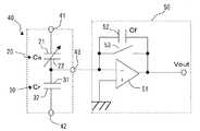
ここで、本発明における容量式湿度センサ10の検出回路の一例を図2に示す。本実施の形態のセンサ10における回路手段は、C−V変換回路(スイッチドキャパシタ回路)50を有し、当該C−V変換回路50は、演算増幅器51、容量値Cfを有するコンデンサ52、及びスイッチ53から構成される。そして、検出部20を構成する検出電極21,22間に生じる容量値Csに比例する電荷と、参照容量部30を構成する参照電極31,32間に生じる容量値Crに比例する電荷との差の電荷を、コンデンサ52に蓄積し電圧に変換して出力するものである。尚、C−V変換回路50は、図示されない回路素子部としてセンサ部40とともに半導体基板12上に設けられて集積化されても良いし、別途外部回路として設けられ、センサ部40の共通電極パッド43に電気的に接続した構成としても良い。
【0034】
演算増幅器51の反転入力端子は、共通電極パッド43を介して検出電極22及び参照電極31に接続されており、反転入力端子と出力端子と間には、コンデンサ52及びスイッチ53が並列に接続されている。また、本実施の形態においては、検出部20と参照容量部30の初期容量差(この場合湿度0%RH)が略同一であるので、演算増幅器51の非反転入力端子はアース接続されている。
【0035】
また、回路手段は図示されない制御回路を有しており、この制御回路は検出電極パッド41から一定振幅Vccで周期的に変化する第1搬送波を検出部20の検出電極21に入力し、参照電極パッド42から、第1搬送波と位相が180°ずれ且つ同一振幅Vccである第2搬送波を参照容量部30の参照電極32に入力する。
【0036】
また、スイッチ53は図示されない制御回路からのクロック信号に同期して生成されるトリガ信号によりオン/オフされ、例えば図3に示すように、第1搬送波の立上がりタイミング(第2搬送波の立ち下がりタイミング)で一定時間(第1搬送波の1/2周期より短い時間)だけオンするように設定される。
【0037】
図3に示すように、検出期間T1において、スイッチ53がオンされるとコンデンサ52が放電され、続いてスイッチ53をオフすると検出電極21,22間と参照電極間31,32間から電荷(Cs−Cr)×Vccが放出され、この電荷がコンデンサ52に蓄積される。従って、演算増幅器51の出力端子にセンサ部40の容量差(Cs−Cr)と振幅Vccに応じた電圧Voutが生じる。この電圧Voutは次式で示される。
【0038】
【数1】
Vout=(Cs−Cr)×Vcc/Cf
このとき、周囲の湿度変化に応じて、参照容量部30の容量値Crは変化せず、検出部20の容量値Csは変化する。従って、数式1に示される電圧Voutを検出することにより、湿度を検出することができる。尚、この電圧Voutは、この後、増幅回路やローパスフィルタ等を備えた図示されない信号処理回路にて信号処理され、湿度検出信号として検出される。
【0039】
次に、容量式湿度センサ10の製造方法について、図1(b)を用いて説明する。
【0040】
先ず、半導体基板12の表面に、CVD法等により第1絶縁膜11であるシリコン酸化膜を形成する。
【0041】
第1絶縁膜11形成後、検出電極21,22及び参照電極31,32を、Al等を用い蒸着法等により第1絶縁膜11上に形成する。尚、検出電極パッド41、参照電極パッド42、及び共通電極パッド43も同時に形成される。そして、検出電極21,22及び参照電極31,32を覆うように第2絶縁膜13であるシリコン窒化膜をプラズマCVD法等にて形成する。
【0042】
続いて図示されないが、検出電極パッド41、参照電極パッド42、及び共通電極パッド43の少なくとも1つが外部回路等と接続される際には、当該パッド上の第2絶縁膜13を、フォトリソグラフを用いたエッチングにより除去する。
【0043】
そして、第2絶縁膜13上の検出部20の領域に、例えば印刷法により所定パターンに塗布し硬化する方法やスピンコート法を用いてポリイミドを塗布し硬化させフォトエッチする方法により感湿膜23を形成する。
【0044】
また、ポッティング等により、第2絶縁膜13上の参照容量部30の領域にシリコンゲルを塗布し、容量調整膜としての透湿膜33を形成する。尚、半導体基板12にC−V変換回路50等の回路素子部を形成する際は、第1絶縁膜11の形成前に、従来の半導体製造技術を用いて形成する。
【0045】
このようにして形成された容量式湿度センサ10において、容量調整膜としての透湿膜33形成による初期容量差(オフセット電圧)低減の効果は、シミュレーションからも明らかである。その結果を図4に示す。センサ構成は上述同様とし、湿度0%RHにおいて誘電率3.4のポリイミドを感湿膜23とし、誘電率3.2のシリコンゲルを透湿膜33とした。図4に示すように、透湿膜33を参照電極31,32上に設けることにより、湿度0%RHにおける検出部20と参照容量部30との初期容量差(Cs−Cr)を小さくできることがわかる。また、実際に同様のセンサ構成を有する容量式湿度センサ10と、透湿膜30を有さない容量式湿度センサを形成し容量差を比較したところ、透湿膜30を設けたセンサ10の容量差は透湿膜30がないセンサの容量差の約1/8となった。
【0046】
ここで、センサ出力範囲が例えば0〜5Vであるとすると、仮にオフセット電圧が2V生じた場合には、湿度検出のために3Vの出力範囲しか取れないため、湿度の検出精度が低下する。従来の容量式湿度センサにおいては、この問題を解決するために、別途オフセット補正回路を設けたり、容量電極31,32を大きくして、オフセット電圧を補正していた。
【0047】
しかしながら、本実施の形態における容量式湿度センサ10は、センサ部40の一部として参照電極31,32上に容量調整膜を設けることにより、初期容量差を小さくし、簡便にオフセット電圧を低減することができる。従って、オフセット電圧低減のために、オフセット補正回路を設けたり、参照容量部30の参照電極31,32の電極パターンを大型化する必要がないので、センサ10の体格を小型化することができる。
【0048】
また、検出電極21,22と参照電極31,32の電極パターンが略同一であれば、参照電極31,32の電極パターン設計を別途する必要がなく、同一工程で両電極21,22,31,32を一括形成することもできるので、製造工程を簡略化することができる。
【0049】
尚、湿度が基準状態(例えば湿度0%RH)であるときの透湿膜33の誘電率が感湿膜23の誘電率よりも大きい場合には、参照電極31,32の電極パターンを小さくすることにより、初期容量差を低減することもできる。この場合、センサ体格をより小型化することができるが、別途参照電極31,32のパターン設計を行う手間が生じる。このように、検出電極21,22と参照電極31,32の電極パターンを必ずしも略同一にする必要はないが、別途電極パターンの設計を行う必要があるため、略同一とするほうが好ましい。
【0050】
また、本実施の形態において、湿度0%RHにおける感湿膜23の誘電率と略等しい誘電率を有する透湿膜33を用い、湿度0%RHにおける初期容量差を小さくし、オフセット電圧を低減する例を示した。しかしながら、それ以外にも、例えば湿度100%RHを基準状態として、湿度100%RHにおける感湿膜23の誘電率と略等しい誘電率を有する透湿膜33を用い、湿度100%RHにおける初期容量差を小さくし、オフセット電圧を低減しても良い。この場合、図3において、スイッチ53のオン/オフタイミングを変更し、第2搬送波の立上がりタイミング(第1搬送波の立ち下がりタイミング)で一定時間だけオンするように設定し、第1搬送波がローレベル、第2搬送波がハイレベルの期間において出力電圧Voutを検出すればよい。また、それ以外にも、湿度50%RHを基準状態としても良い。
【0051】
また、本実施の形態において、センサ10の出力範囲を広くとるために演算増幅器51の非反転入力端子をアース電位とした。しかしながら、所定の電位を基準電位として入力することもできる。例えば、容量調整膜の大きさや厚さにより初期容量差はできるだけ小さくなるように調整されるが、それでも初期容量差が生じた場合には、中点電位に相当する電位を基準電位として非反転入力端子に入力しても良い。また、上記湿度50%RHを基準状態とする場合には、Vcc/2を非反転入力端子に入力すれば良い。
【0052】
また、本実施の形態においては、容量調整膜として透湿膜33を参照電極31,32上にのみ形成する例を示した。しかしながら、透湿膜33は水分を透過するので、図5に示すように、参照容量部30(感湿膜23上)とともに検出部20に設けても良い。検出電極21,22上にも第2絶縁膜13及び感湿膜23を介して透湿膜33が形成されれば、透湿膜33が周囲の湿度の影響を受けて誘電率が変化したとしても、透湿膜33の容量変化に与える影響分を相殺することができ、より精度良く湿度を検出することができる。
【0053】
また、センサ構造としては、センサ部40直下の半導体基板12が削除されたメンブレン構造であっても良い。
【0054】
(第2の実施の形態)
次に、本発明の第2の実施の形態を、図6に示す容量式湿度センサ10の断面図に基づいて説明する。
【0055】
第2の実施の形態における容量式湿度センサ10は、第1の実施の形態によるものと共通するところが多いので、以下、共通部分については詳しい説明は省略し、異なる部分を重点的に説明する。
【0056】
第2の実施の形態において、第1の実施の形態と異なる点は、容量調整膜として透湿膜23の替わりに、感湿膜23と非透湿膜を形成した点である。
【0057】
図6に示すように、検出電極21,22及び参照電極31,32は同一平面上に形成され、その上部に第2絶縁膜13であるシリコン窒化膜が形成されている。尚、検出電極21,22と参照電極31,32の両電極パターンは略同一である。そして、第2絶縁膜13上のセンサ部40領域(検出部20領域+参照容量部30領域)に、例えばポリイミドからなる感湿膜23が形成されている。
【0058】
従って、湿度0%RHにおける検出部20の容量値Csと参照容量部30の容量値Crが略等しくなるので、オフセット電圧をほぼ0とすることができる。
【0059】
さらに、参照容量部30の感湿膜23上には、非透湿膜60が形成されている。非透湿膜60は、水分を透過しない(感湿膜23への水分を遮断する)材料をもとに構成され、例えばシリコン酸化膜やシリコン窒化膜を用いることができる。尚、本実施の形態においてはシリコン窒化膜を用いるものとし、プラズマCVD法等により形成するものとする。
【0060】
従って、周囲の湿度変化に応じて検出部20側の感湿膜23の誘電率が変化し、検出部20の容量値Csが変化するのに対し、参照容量部30側の感湿膜23は非透湿膜60にて水分が遮断されるので、誘電率が変化せず参照容量部30の容量値Crも一定の値を示すこととなる。
【0061】
このように、本実施の形態における容量式湿度センサ10は、参照容量部30に容量調整膜の一部として検出部20同様感湿膜23を備えているので、湿度0%RHにおける検出部20の容量値Csと参照容量部30の容量値Crとの初期容量差を小さくすることができる。特に、検出電極21,22と参照電極31,32とが同一パターンであると、湿度0%RHにおける容量差をほぼ0とでき、オフセット電圧をより低減することができる。
【0062】
そして、参照容量部30は感湿膜23上に容量調整膜の一部として非透湿膜60を備えているので、湿度が変化しても参照電極31,32間の容量値Crはほぼ一定の値を示すことができる。従って、本実施の形態における容量式湿度センサ10は、湿度を精度良く検出することができる。
【0063】
また、オフセット電圧低減のために、オフセット補正回路を設けたり、参照容量部30の参照電極31,32の電極パターンを大型化する必要がなく、参照容量部30に容量調整膜として感湿膜23と非透湿膜60を設けるだけであるので、簡便にオフセット電圧を低減でき、センサ10の体格を小型化することができる。
【0064】
さらに、本実施の形態においても、検出電極21,22と参照電極31,32の電極パターンが略同一であれば、参照電極31,32の電極パターン設計を別途する必要がなく、同一工程で両電極21,22,31,32を一括形成することもできるので、製造工程を簡略化することができる。
【図面の簡単な説明】
【図1】 本発明の第1実施形態における容量式湿度センサの概略を示す図であり、(a)は部分平面図、(b)は(a)のA−A断面における断面図である。
【図2】 検出回路を示すブロック図である。
【図3】 図3に示す検出回路に対するタイミングチャートの一例を示す図である。
【図4】 透湿膜の効果を示す図である。
【図5】 第1実施形態の変形例を示す断面図である。
【図6】 第2実施形態における容量式湿度センサの断面図である。
【符号の説明】
10・・・容量式湿度センサ
11・・・第1絶縁膜
12・・・半導体基板
13・・・第2絶縁膜
20・・・検出部
21,22・・・検出電極
23・・・感湿膜
30・・・参照容量部
31,32・・・参照電極
33・・・透湿膜
60・・・非透湿膜[0001]
BACKGROUND OF THE INVENTION
The present invention relates to a capacitive humidity sensor.
[0002]
[Prior art]
The present applicant has previously disclosed Patent Document 1 as a capacitive humidity sensor that detects humidity from a capacitance change between two detection electrodes provided on a semiconductor substrate.
[0003]
This sensor has two detection electrodes opposed to each other via a first insulating film on the surface of a semiconductor substrate, and these detection electrodes are covered with a moisture sensitive film via a second insulating film. Yes. In addition, the semiconductor substrate is provided with a reference capacitor portion having a reference capacitor whose capacitance value does not change even when the humidity changes.
[0004]
The detection electrode and the circuit element portion including the reference capacitance portion constitute a switched capacitor (SC) circuit for converting a capacitance change between the detection electrodes into a voltage signal and outputting the voltage signal. Therefore, the humidity can be detected based on the difference between the reference capacity of the reference capacity section and the capacity between the detection electrodes that changes according to the humidity.
[0005]
[Patent Document 1]
Japanese Patent Laid-Open No. 14-243690 [0006]
[Problems to be solved by the invention]
Here, the reference capacitance part in the capacitive humidity sensor of Patent Document 1 is configured by a semiconductor substrate and a wiring electrode provided on the semiconductor substrate, and between the opposing surfaces between the semiconductor substrate and the wiring electrode. A first insulating film having a dielectric constant different from that of the moisture sensitive film is disposed. In such a case, when the humidity is in a reference state (
[0007]
However, in order to reduce the offset voltage in the capacitive humidity sensor shown in Patent Document 1, for example, the wiring electrode pattern of the reference capacitor portion is enlarged so that the surface area facing the semiconductor substrate increases, or the generated offset voltage An offset correction circuit for correcting the above must be provided as a part of the circuit element portion. In this case, it takes time to design a wiring electrode and a correction circuit separately. Moreover, since the formation area of a circuit element part also becomes large, it is difficult to reduce a sensor physique.
[0008]
In view of the above problems, an object of the present invention is to provide a capacitive humidity sensor that can easily reduce the offset voltage and can reduce the size of the sensor.
[0009]
[Means for Solving the Problems]
In order to achieve the above object, a capacitive humidity sensor according to claim 1 is formed on a semiconductor substrate, a pair of detection electrodes opposed to each other on the semiconductor substrate, and a pair of detection electrodes. A detection unit including a moisture sensitive film whose capacitance value changes in response to the detection unit, and a reference capacitance unit including a pair of reference electrodes disposed opposite to each other on the semiconductor substrate, wherein the capacitance value between the detection electrodes and the capacitance between the reference electrodes The difference from the value is converted into a voltage signal to detect humidity. The reference capacitance unit includes a moisturepermeable filmon the reference electrode as a capacitance adjustment film for reducing a capacitance difference when the humidity is in a standard state,and the moisture permeable film is provided on the moisture sensitive film of the detection unit. Is also provided .
[0010]
As described above, this sensor includes a capacitance adjusting film for reducing a capacitance difference (initial capacitance difference) when the humidity is in a standard state (
[0011]
In addition, since onlythe moisture permeable film as the capacity adjustment film is providedin the reference capacitor portion, the offset voltage can be easily reduced, and it is not necessary to install an offset correction circuit or increase the size of the reference electrode pattern. Therefore, the size of the sensor can be reduced.Further, a moisture permeable film is employed as the capacity adjusting film, and the moisture permeable film is also provided on the moisture sensitive film of the detection unit. That is, a moisture permeable film is provided in both the detection unit and the reference capacitance unit. Therefore, even if the moisture permeable membrane is affected by water vapor (hereinafter referred to as moisture) in the gas and its dielectric constant changes, the influence of the moisture permeable membrane on the capacitance change can be offset and reduced. Humidity can be detected well.
[0012]
As described in
[0013]
If both the electrode shape and size (electrode pattern) of the detection electrode and the reference electrode are substantially equal, and the relative humidity of themoisture- sensitive film and themoisture-permeable film when the humidity is in the standard state, the initial capacitance difference is set to approximately zero. Therefore, the offset voltage can be almost zero.
[0014]
Further, since both electrode patterns of the detection electrode and the reference electrode are substantially the same, the electrode pattern design is easy, and both electrodes can be formed in the same process, so that the manufacturing process can be simplified.
[0016]
Specifically, a gel film may be used as the moisture permeable film as described inclaim 3 . If it is a gel film, it can permeate moisture, and the humidity shows a dielectric constant substantially equal to the dielectric constant of the moisture sensitive film in the reference state (for example, polyimide as the moisture sensitive film, silicon gel as the moisture permeable film). It can be suitably used as a moisture permeable membrane.
[0020]
According to a fourth aspect of the present invention, the pair of detection electrodes are preferably provided in a comb-teeth shape so as to mesh with each other. By adopting such a comb-like electrode configuration, the facing area can be increased, so that a larger capacitance value can be obtained in a small space.
[0021]
According to a fifth aspect of the present invention , the first insulating film is provided between the semiconductor substrate, the detection electrode, and the reference electrode, and the second insulating film is interposed between the detection electrode and the moisture sensitive film and between thereference electrode and the moisture permeable film . It is preferable to provide an insulating film. As described above, the first and second insulating films ensure the insulation, and the second insulating film can also ensure the moisture resistance of the electrode, thereby improving the reliability of the sensor.
[0022]
DETAILED DESCRIPTION OF THE INVENTION
Hereinafter, embodiments of the present invention will be described with reference to the drawings.
(First embodiment)
FIG. 1A is a partial plan view showing an outline of a capacitive humidity sensor in the present embodiment, and FIG. 1B is a cross-sectional view taken along a line AA in FIG. In FIG. 1 (a), for the sake of convenience, the detection electrode immediately below the second insulating film and the moisture sensitive film and the reference electrode directly below the second insulating film and the capacitance adjusting film are shown in FIG. Both electrodes are hatched. Note that the capacitive humidity sensor of the present embodiment is used for humidity control of an air conditioner, and is used for detecting indoor humidity or detecting outdoor humidity for weather observation.
[0023]
The
[0024]
The
[0025]
The
[0026]
Here, the pair of
[0027]
A silicon nitride film as the second insulating
[0028]
Further, a moisture
[0029]
The moisture
[0030]
Further, as shown in FIG. 1B, the moisture
[0031]
The capacitance adjusting film has a capacitance difference between the capacitance value between the
[0032]
The capacitive humidity sensor 1 according to the present embodiment has the
[0033]
Here, an example of the detection circuit of the
[0034]
The inverting input terminal of the
[0035]
Further, the circuit means has a control circuit (not shown). This control circuit inputs a first carrier wave that periodically changes with a constant amplitude Vcc from the
[0036]
The
[0037]
As shown in FIG. 3, during the detection period T1, when the
[0038]
[Expression 1]
Vout = (Cs−Cr) × Vcc / Cf
At this time, the capacitance value Cr of the
[0039]
Next, a manufacturing method of the
[0040]
First, a silicon oxide film that is the first insulating
[0041]
After the first insulating
[0042]
Subsequently, although not shown, when at least one of the
[0043]
Then, the moisture
[0044]
Further, silicon gel is applied to the region of the
[0045]
In the
[0046]
Here, assuming that the sensor output range is 0 to 5 V, for example, if an offset voltage of 2 V is generated, only an output range of 3 V can be obtained for humidity detection, so that the humidity detection accuracy is lowered. In the conventional capacitive humidity sensor, in order to solve this problem, an offset correction circuit is separately provided or the
[0047]
However, the
[0048]
Further, if the electrode patterns of the
[0049]
If the dielectric constant of the moisture
[0050]
In the present embodiment, the moisture
[0051]
In the present embodiment, the non-inverting input terminal of the
[0052]
Further, in the present embodiment, an example in which the moisture
[0053]
The sensor structure may be a membrane structure in which the
[0054]
(Second Embodiment)
Next, a second embodiment of the present invention will be described based on a sectional view of the
[0055]
Since the
[0056]
The second embodiment is different from the first embodiment in that a moisture-
[0057]
As shown in FIG. 6, the
[0058]
Accordingly, since the capacitance value Cs of the
[0059]
Furthermore, a moisture-
[0060]
Therefore, the dielectric constant of the moisture
[0061]
As described above, the
[0062]
And since the reference capacity |
[0063]
Further, in order to reduce the offset voltage, it is not necessary to provide an offset correction circuit or increase the size of the electrode pattern of the
[0064]
Furthermore, also in this embodiment, if the electrode patterns of the
[Brief description of the drawings]
1A and 1B are diagrams schematically illustrating a capacitive humidity sensor according to a first embodiment of the present invention, where FIG. 1A is a partial plan view, and FIG. 1B is a cross-sectional view taken along a line AA in FIG.
FIG. 2 is a block diagram illustrating a detection circuit.
FIG. 3 is a diagram showing an example of a timing chart for the detection circuit shown in FIG. 3;
FIG. 4 is a diagram showing the effect of a moisture permeable membrane.
FIG. 5 is a cross-sectional view showing a modification of the first embodiment.
FIG. 6 is a cross-sectional view of a capacitive humidity sensor according to a second embodiment.
[Explanation of symbols]
DESCRIPTION OF
Claims (5)
Translated fromJapanese当該半導体基板上に対向配置された一対の検出電極と、前記一対の検出電極上に形成され、湿度に応じて容量値が変化する感湿膜とを備える検出部と、
前記半導体基板上に対向配置された一対の参照電極からなる参照容量部とを備え、
前記検出電極間の容量値と前記参照電極間の容量値との容量差を電圧信号に変換して湿度を検出する容量式湿度センサであって、
前記参照容量部は、前記湿度が基準状態である場合の前記容量差を低減するための容量調整膜として、透湿膜を前記参照電極上に備えており、
前記透湿膜は、前記検出部の前記感湿膜上にも設けられていることを特徴とする容量式湿度センサ。A semiconductor substrate;
A detection unit comprising a pair of detection electrodes opposed to each other on the semiconductor substrate, and a moisture-sensitive film formed on the pair of detection electrodes and having a capacitance value that changes according to humidity;
A reference capacitance unit composed of a pair of reference electrodes opposed to each other on the semiconductor substrate,
A capacitive humidity sensor that detects humidity by converting a capacitance difference between a capacitance value between the detection electrodes and a capacitance value between the reference electrodes into a voltage signal,
The reference capacity unit includes a moisturepermeable filmon the reference electrode as a capacity adjustment film for reducing the capacity difference when the humidity is in a standard state.
The moisture permeable film is also provided on the moisturesensitive film of the detection unit .
Priority Applications (2)
| Application Number | Priority Date | Filing Date | Title |
|---|---|---|---|
| JP2003075017AJP3855950B2 (en) | 2003-03-19 | 2003-03-19 | Capacitive humidity sensor |
| US10/797,117US7032448B2 (en) | 2003-03-19 | 2004-03-11 | Capacitive humidity sensor |
Applications Claiming Priority (1)
| Application Number | Priority Date | Filing Date | Title |
|---|---|---|---|
| JP2003075017AJP3855950B2 (en) | 2003-03-19 | 2003-03-19 | Capacitive humidity sensor |
Publications (2)
| Publication Number | Publication Date |
|---|---|
| JP2004279370A JP2004279370A (en) | 2004-10-07 |
| JP3855950B2true JP3855950B2 (en) | 2006-12-13 |
Family
ID=32984767
Family Applications (1)
| Application Number | Title | Priority Date | Filing Date |
|---|---|---|---|
| JP2003075017AExpired - Fee RelatedJP3855950B2 (en) | 2003-03-19 | 2003-03-19 | Capacitive humidity sensor |
Country Status (2)
| Country | Link |
|---|---|
| US (1) | US7032448B2 (en) |
| JP (1) | JP3855950B2 (en) |
Families Citing this family (60)
| Publication number | Priority date | Publication date | Assignee | Title |
|---|---|---|---|---|
| JP2005106802A (en)* | 2003-07-10 | 2005-04-21 | Canon Inc | Environmental sensor, environmental measuring device and environmental measuring system |
| JP4455286B2 (en)* | 2004-11-09 | 2010-04-21 | 株式会社日本自動車部品総合研究所 | Capacitive humidity sensor |
| JP4566784B2 (en)* | 2005-02-24 | 2010-10-20 | 株式会社デンソー | Humidity sensor device |
| JP4770220B2 (en)* | 2005-03-23 | 2011-09-14 | 旭硝子株式会社 | Condensation detection sensor and vehicle window plate |
| US7373819B2 (en)* | 2005-09-30 | 2008-05-20 | Honeywell International Inc. | Stress sensitive humidity sensor based on a MEMS structure |
| JP4770530B2 (en)* | 2006-03-13 | 2011-09-14 | 株式会社デンソー | Capacitive humidity sensor |
| US7456744B2 (en)* | 2006-05-16 | 2008-11-25 | 3M Innovative Properties Company | Systems and methods for remote sensing using inductively coupled transducers |
| TWI314989B (en)* | 2006-06-23 | 2009-09-21 | Fego Prec Ind Co Ltd | Humidity sensor having temperature compensation self-comparing and manufacturing method therefore |
| US20080191716A1 (en)* | 2007-02-08 | 2008-08-14 | International Business Machines Corporation | On-Chip Real-Time Moisture Sensor For and Method of Detecting Moisture Ingress in an Integrated Circuit Chip |
| JP4386295B2 (en)* | 2007-04-20 | 2009-12-16 | 株式会社日本自動車部品総合研究所 | Humidity sensor |
| US7764069B2 (en)* | 2007-04-25 | 2010-07-27 | International Business Machines Corporation | Process for measuring bond-line thickness |
| US7571637B2 (en)* | 2007-10-29 | 2009-08-11 | International Business Machines Corporation | Design structure for an on-chip real-time moisture sensor for and method of detecting moisture ingress in an integrated circuit chip |
| JP2009111110A (en)* | 2007-10-30 | 2009-05-21 | Nec Electronics Corp | Semiconductor device |
| US8192427B2 (en)* | 2008-06-09 | 2012-06-05 | Tyco Healthcare Group Lp | Surface ablation process with electrode cooling methods |
| CN102639993B (en)* | 2009-12-22 | 2015-03-25 | 纳米及先进材料研发院有限公司 | Rapid-response relative humidity sensor applying anodic aluminum oxide film |
| US8564311B2 (en)* | 2010-07-01 | 2013-10-22 | Stmicroelectronics Asia Pacific Pte Ltd. | Sensing phase sequence to suppress single tone noise |
| JP5547296B2 (en)* | 2010-10-04 | 2014-07-09 | アルプス電気株式会社 | Humidity detection sensor and manufacturing method thereof |
| US9086368B2 (en)* | 2011-02-24 | 2015-07-21 | International Business Machines Corporation | Non-destructive determination of the moisture content in an electronic circuit board using comparison of capacitance measurements acquired from test coupons, and design structure/process therefor |
| MY154211A (en)* | 2011-04-26 | 2015-05-15 | Mimos Berhad | A humidity sensor device |
| US9360445B2 (en) | 2011-12-21 | 2016-06-07 | Carlsen Melton, Inc. | Relative humidity and condensation measurement with a capacitive humidity sensor |
| JP2014010011A (en)* | 2012-06-28 | 2014-01-20 | Denso Corp | Humidity sensor |
| US9304098B2 (en)* | 2013-02-04 | 2016-04-05 | Veris Industries, Llc | Capacitive humidity sensor with hysteresis compensation |
| DE102014202248A1 (en)* | 2014-02-07 | 2015-08-27 | Robert Bosch Gmbh | Sensor for detecting at least one medium and method for operating a capacitive measuring device |
| JP6228865B2 (en)* | 2014-03-06 | 2017-11-08 | アルプス電気株式会社 | Sensor device inspection method and sensor device |
| JP6641701B2 (en) | 2014-03-14 | 2020-02-05 | 株式会社リコー | Atmosphere sensor, method for manufacturing the same, and method for manufacturing printed matter |
| DE102014210122B4 (en)* | 2014-05-27 | 2025-04-30 | Robert Bosch Gmbh | Device for determining a value of a property of a fluid to be measured, method for operating a device for determining a value of a property of a fluid to be measured |
| KR102237710B1 (en) | 2014-06-18 | 2021-04-09 | 주식회사 해치텍 | Capacitor type Humidity Sensor |
| KR102187614B1 (en) | 2014-07-02 | 2020-12-08 | 주식회사 키 파운드리 | Capacitor type Humidity Sensor |
| CN105806900A (en)* | 2014-08-20 | 2016-07-27 | 云南师范大学 | Humidity detection circuit |
| EP3078964B1 (en)* | 2015-04-09 | 2017-05-24 | Honeywell International Inc. | Relative humidity sensor and method |
| JP6515683B2 (en)* | 2015-05-29 | 2019-05-22 | 富士通株式会社 | Measuring device and measuring system |
| US9696272B2 (en)* | 2015-08-07 | 2017-07-04 | Silicon Laboratories Inc. | Systems and methods for humidity measurement using dielectric material-based relative humidity sensors |
| US11026481B2 (en) | 2016-03-15 | 2021-06-08 | Nike, Inc. | Foot presence signal processing using velocity |
| US11357290B2 (en) | 2016-03-15 | 2022-06-14 | Nike, Inc. | Active footwear sensor calibration |
| KR102494900B1 (en) | 2016-03-15 | 2023-02-01 | 나이키 이노베이트 씨.브이. | Capacitive Foot Presence Detection for Footwear |
| US11064768B2 (en) | 2016-03-15 | 2021-07-20 | Nike, Inc. | Foot presence signal processing using velocity |
| US11815504B2 (en)* | 2016-07-11 | 2023-11-14 | Quipip, Llc | Sensor device, and systems and methods for obtaining measurements of selected characteristics of a concrete mixture |
| KR101905961B1 (en)* | 2016-07-26 | 2018-11-21 | 현대자동차주식회사 | Occupant classification apparatus |
| CN106198651A (en)* | 2016-08-31 | 2016-12-07 | 成都市和平科技有限责任公司 | A kind of high accuracy humidity sensor |
| WO2018056062A1 (en)* | 2016-09-21 | 2018-03-29 | 東洋紡株式会社 | Stretchable capacitor, deformation sensor, displacement sensor, method for sensing respiration state, and sensing wear |
| US10172392B2 (en) | 2016-11-18 | 2019-01-08 | Rai Strategic Holdings, Inc. | Humidity sensing for an aerosol delivery device |
| DE102018005010A1 (en)* | 2017-07-13 | 2019-01-17 | Wika Alexander Wiegand Se & Co. Kg | Transfer and melting of layers |
| CN107589155A (en)* | 2017-09-12 | 2018-01-16 | 华南师范大学 | A kind of capacitance type sensor and preparation method thereof |
| KR101830304B1 (en) | 2017-10-17 | 2018-02-21 | 인창전자주식회사 | Fabrication method of integrated sensor and integrated sensor using the same |
| KR101976461B1 (en)* | 2017-11-24 | 2019-05-10 | 주식회사 신우전자 | Vertical layered temperature-humidity hybrid sensor and manufacturing method for the sensor |
| EP3499225B1 (en)* | 2017-12-18 | 2021-01-27 | Stichting IMEC Nederland | Conductivity sensor with adjustable cell constant |
| EP3540422B1 (en)* | 2018-03-14 | 2024-01-03 | Sciosense B.V. | Monolithic gas sensor arrangement, manufacturing method and measurement method |
| US11313824B2 (en)* | 2018-11-16 | 2022-04-26 | Minebea Mitsumi Inc. | Detecting device |
| JP7193203B2 (en)* | 2018-11-16 | 2022-12-20 | ミネベアミツミ株式会社 | detector |
| CN209326840U (en) | 2018-12-27 | 2019-08-30 | 热敏碟公司 | Pressure sensor and pressure transmitter |
| EP3699583A1 (en) | 2019-02-21 | 2020-08-26 | Sensirion AG | Capacitive sensor |
| KR102264196B1 (en)* | 2019-03-13 | 2021-06-14 | 주식회사 이너센서 | Sensor module and method of automatically adjusting the same |
| JP7096635B2 (en)* | 2019-03-22 | 2022-07-06 | 株式会社日立製作所 | Moisture detection element, breath gas detection device, breath test system and manufacturing method of moisture detection element |
| CN110243883B (en)* | 2019-06-18 | 2020-06-12 | 福州大学 | Relative humidity fitting method suitable for HS 1101-based intelligent humidity sensing system |
| JP2021092453A (en)* | 2019-12-11 | 2021-06-17 | ミネベアミツミ株式会社 | Humidity sensor |
| US11581206B2 (en)* | 2020-03-06 | 2023-02-14 | Applied Materials, Inc. | Capacitive sensor for chamber condition monitoring |
| JP6884900B2 (en)* | 2020-03-12 | 2021-06-09 | 株式会社東芝 | Gas detector |
| CN112268941B (en)* | 2020-09-17 | 2025-07-15 | 华帝股份有限公司 | Capacitive humidity sensor and cooking equipment |
| WO2023182075A1 (en)* | 2022-03-23 | 2023-09-28 | ラピステクノロジー株式会社 | Semiconductor device, and capacitive sensor device |
| US20230363956A1 (en)* | 2022-05-12 | 2023-11-16 | Flexible Technologies, Inc. | Moisture detection system, method for use of system, and laminate for system |
Family Cites Families (25)
| Publication number | Priority date | Publication date | Assignee | Title |
|---|---|---|---|---|
| JPS5431714B2 (en)* | 1972-09-20 | 1979-10-09 | ||
| US4419888A (en)* | 1979-06-14 | 1983-12-13 | Kabushikikaisha Shibaura Denshi Seisakusho | Humidity measuring method |
| JPS57109319A (en)* | 1980-12-16 | 1982-07-07 | Yoshio Imai | Capacity type moisture sensor and method of producing same |
| DE3270451D1 (en)* | 1981-09-28 | 1986-05-15 | Hitachi Ltd | Humidity sensor and method for preparing a humidity sensor |
| GB8322418D0 (en)* | 1983-08-19 | 1983-09-21 | Emi Ltd | Humidity sensor |
| US4603372A (en)* | 1984-11-05 | 1986-07-29 | Direction De La Meteorologie Du Ministere Des Transports | Method of fabricating a temperature or humidity sensor of the thin film type, and sensors obtained thereby |
| US4928513A (en)* | 1986-07-29 | 1990-05-29 | Sharp Kabushiki Kaisha | Sensor |
| DE3919864A1 (en)* | 1989-06-19 | 1990-12-20 | Testoterm Mestechnik Gmbh & Co | CAPACITIVE HUMIDITY SENSOR |
| JPH05506711A (en)* | 1989-08-29 | 1993-09-30 | エー ウント エー エレクトロニク ゲゼルシャフト エム ベー ハー | Method of using swellable plastic to manufacture a resistive humidity sensor and method of manufacturing a resistive humidity sensor |
| US5036704A (en)* | 1990-03-23 | 1991-08-06 | Gas Research Institute | Moisture sensor |
| DK0475025T3 (en)* | 1990-09-12 | 1995-06-19 | Endress Hauser Gmbh Co | Process for producing a capacitive moisture sensor |
| US5837884A (en)* | 1994-12-29 | 1998-11-17 | Tokin Corporation | Humidity sensor using temperature sensing resistor controlled to be at constant temperature of more than 150° C. |
| US5855849A (en)* | 1996-01-16 | 1999-01-05 | Industrial Technology Research Institute | Solid state humidity sensor |
| US5741540A (en)* | 1996-01-16 | 1998-04-21 | Industrial Technology Research Institute | Method of forming solid state humidity sensor |
| US5767687A (en)* | 1996-11-29 | 1998-06-16 | Geist; Jon | Surface-capacitor type condensable-vapor sensor |
| JPH10239264A (en)* | 1997-02-25 | 1998-09-11 | Sanriki Kogyo Kk | Electric resistance type moisture sensor |
| TW571093B (en)* | 1998-12-28 | 2004-01-11 | Tdk Corp | Moisture sensor |
| KR100351810B1 (en)* | 1999-12-13 | 2002-09-11 | 엘지전자 주식회사 | absolute humidity sensor |
| DE10002707A1 (en)* | 2000-01-22 | 2001-08-02 | Bosch Gmbh Robert | Gas sensor |
| KR100379471B1 (en)* | 2000-07-19 | 2003-04-10 | 엘지전자 주식회사 | absolute humidity sensor and circuit for detecting temperature and humidity using the same |
| JP2002243689A (en)* | 2001-02-15 | 2002-08-28 | Denso Corp | Capacity-type humidity sensor and method for manufacturing the same |
| US6580600B2 (en) | 2001-02-20 | 2003-06-17 | Nippon Soken, Inc. | Capacitance type humidity sensor and manufacturing method of the same |
| EP1369683A4 (en)* | 2001-03-13 | 2008-06-18 | Tdk Corp | Humidity sensor element and method for manufacture thereof |
| JP2003004683A (en)* | 2001-06-15 | 2003-01-08 | Denso Corp | Capacitive humidity sensor |
| JP4501320B2 (en)* | 2001-07-16 | 2010-07-14 | 株式会社デンソー | Capacitive humidity sensor |
- 2003
- 2003-03-19JPJP2003075017Apatent/JP3855950B2/ennot_activeExpired - Fee Related
- 2004
- 2004-03-11USUS10/797,117patent/US7032448B2/ennot_activeExpired - Fee Related
Also Published As
| Publication number | Publication date |
|---|---|
| JP2004279370A (en) | 2004-10-07 |
| US20040182153A1 (en) | 2004-09-23 |
| US7032448B2 (en) | 2006-04-25 |
Similar Documents
| Publication | Publication Date | Title |
|---|---|---|
| JP3855950B2 (en) | Capacitive humidity sensor | |
| JP4229885B2 (en) | Capacitive physical quantity detector | |
| JP4770530B2 (en) | Capacitive humidity sensor | |
| JP4501320B2 (en) | Capacitive humidity sensor | |
| JP6732105B2 (en) | Capacitance detection module, method and electronic device | |
| TWI835954B (en) | Micromechanical component for a capacitive pressure sensor device | |
| JP2004271461A (en) | Capacitance type humidity sensor | |
| JP2003270189A (en) | Capacitive humidity sensor | |
| WO2010113711A1 (en) | Capacitive humidity sensor and manufacturing method therefor | |
| US7710128B2 (en) | Method and apparatus for controlling the sensitivity and value of a capacitive humidity sensor | |
| US20020109959A1 (en) | Capacitive moisture sensor and fabrication method for capacitive moisture sensor | |
| JPH0726886B2 (en) | Integrated capacitive pressure sensor and method of manufacturing the same | |
| JP2002243690A (en) | Capacitance type humidity sensor and method for manufacturing the same | |
| EP2257824A1 (en) | Method and system for adjusting characteristics of integrated relative humidity sensor | |
| CN114705724B (en) | Drift-free humidity sensor | |
| US7543503B2 (en) | Deformation detection sensor with temperature correction | |
| US6370960B1 (en) | Capacitive sensor | |
| TW202237524A (en) | Pressure sensor and method for operating a pressure sensor | |
| JP4475070B2 (en) | Humidity sensor | |
| JP2012145384A (en) | Capacitive humidity sensor | |
| JPH10132684A (en) | Semiconductor pressure sensor | |
| CN114136503B (en) | Method for integrating pressure sensor and humidity sensor | |
| JP2572752Y2 (en) | pressure sensor | |
| JP4650246B2 (en) | Humidity sensor | |
| JP2001272414A (en) | Sensor for detecting knocking of internal engine |
Legal Events
| Date | Code | Title | Description |
|---|---|---|---|
| A621 | Written request for application examination | Free format text:JAPANESE INTERMEDIATE CODE: A621 Effective date:20050427 | |
| A977 | Report on retrieval | Free format text:JAPANESE INTERMEDIATE CODE: A971007 Effective date:20060414 | |
| A131 | Notification of reasons for refusal | Free format text:JAPANESE INTERMEDIATE CODE: A131 Effective date:20060425 | |
| A521 | Request for written amendment filed | Free format text:JAPANESE INTERMEDIATE CODE: A523 Effective date:20060621 | |
| TRDD | Decision of grant or rejection written | ||
| A01 | Written decision to grant a patent or to grant a registration (utility model) | Free format text:JAPANESE INTERMEDIATE CODE: A01 Effective date:20060822 | |
| A61 | First payment of annual fees (during grant procedure) | Free format text:JAPANESE INTERMEDIATE CODE: A61 Effective date:20060904 | |
| R150 | Certificate of patent or registration of utility model | Free format text:JAPANESE INTERMEDIATE CODE: R150 | |
| FPAY | Renewal fee payment (event date is renewal date of database) | Free format text:PAYMENT UNTIL: 20090922 Year of fee payment:3 | |
| FPAY | Renewal fee payment (event date is renewal date of database) | Free format text:PAYMENT UNTIL: 20100922 Year of fee payment:4 | |
| FPAY | Renewal fee payment (event date is renewal date of database) | Free format text:PAYMENT UNTIL: 20100922 Year of fee payment:4 | |
| FPAY | Renewal fee payment (event date is renewal date of database) | Free format text:PAYMENT UNTIL: 20110922 Year of fee payment:5 | |
| FPAY | Renewal fee payment (event date is renewal date of database) | Free format text:PAYMENT UNTIL: 20110922 Year of fee payment:5 | |
| FPAY | Renewal fee payment (event date is renewal date of database) | Free format text:PAYMENT UNTIL: 20120922 Year of fee payment:6 | |
| FPAY | Renewal fee payment (event date is renewal date of database) | Free format text:PAYMENT UNTIL: 20120922 Year of fee payment:6 | |
| FPAY | Renewal fee payment (event date is renewal date of database) | Free format text:PAYMENT UNTIL: 20130922 Year of fee payment:7 | |
| R250 | Receipt of annual fees | Free format text:JAPANESE INTERMEDIATE CODE: R250 | |
| LAPS | Cancellation because of no payment of annual fees |