JP3852916B2 - Display device - Google Patents
Display deviceDownload PDFInfo
- Publication number
- JP3852916B2 JP3852916B2JP2001360715AJP2001360715AJP3852916B2JP 3852916 B2JP3852916 B2JP 3852916B2JP 2001360715 AJP2001360715 AJP 2001360715AJP 2001360715 AJP2001360715 AJP 2001360715AJP 3852916 B2JP3852916 B2JP 3852916B2
- Authority
- JP
- Japan
- Prior art keywords
- voltage
- power supply
- transistor
- current
- fet
- Prior art date
- Legal status (The legal status is an assumption and is not a legal conclusion. Google has not performed a legal analysis and makes no representation as to the accuracy of the status listed.)
- Expired - Fee Related
Links
- 239000011159matrix materialSubstances0.000claimsdescription8
- 238000012544monitoring processMethods0.000claimsdescription7
- 239000013643reference controlSubstances0.000claimsdescription7
- 238000005401electroluminescenceMethods0.000claimsdescription4
- 238000010586diagramMethods0.000description14
- 230000032683agingEffects0.000description9
- 239000000463materialSubstances0.000description5
- 230000005669field effectEffects0.000description4
- 230000004044responseEffects0.000description4
- 239000003990capacitorSubstances0.000description3
- 230000000694effectsEffects0.000description1
- 238000000034methodMethods0.000description1
- 230000001360synchronised effectEffects0.000description1
Images


Classifications
- G—PHYSICS
- G09—EDUCATION; CRYPTOGRAPHY; DISPLAY; ADVERTISING; SEALS
- G09G—ARRANGEMENTS OR CIRCUITS FOR CONTROL OF INDICATING DEVICES USING STATIC MEANS TO PRESENT VARIABLE INFORMATION
- G09G3/00—Control arrangements or circuits, of interest only in connection with visual indicators other than cathode-ray tubes
- G09G3/20—Control arrangements or circuits, of interest only in connection with visual indicators other than cathode-ray tubes for presentation of an assembly of a number of characters, e.g. a page, by composing the assembly by combination of individual elements arranged in a matrix no fixed position being assigned to or needed to be assigned to the individual characters or partial characters
- G09G3/22—Control arrangements or circuits, of interest only in connection with visual indicators other than cathode-ray tubes for presentation of an assembly of a number of characters, e.g. a page, by composing the assembly by combination of individual elements arranged in a matrix no fixed position being assigned to or needed to be assigned to the individual characters or partial characters using controlled light sources
- G09G3/30—Control arrangements or circuits, of interest only in connection with visual indicators other than cathode-ray tubes for presentation of an assembly of a number of characters, e.g. a page, by composing the assembly by combination of individual elements arranged in a matrix no fixed position being assigned to or needed to be assigned to the individual characters or partial characters using controlled light sources using electroluminescent panels
- G09G3/32—Control arrangements or circuits, of interest only in connection with visual indicators other than cathode-ray tubes for presentation of an assembly of a number of characters, e.g. a page, by composing the assembly by combination of individual elements arranged in a matrix no fixed position being assigned to or needed to be assigned to the individual characters or partial characters using controlled light sources using electroluminescent panels semiconductive, e.g. using light-emitting diodes [LED]
- G09G3/3208—Control arrangements or circuits, of interest only in connection with visual indicators other than cathode-ray tubes for presentation of an assembly of a number of characters, e.g. a page, by composing the assembly by combination of individual elements arranged in a matrix no fixed position being assigned to or needed to be assigned to the individual characters or partial characters using controlled light sources using electroluminescent panels semiconductive, e.g. using light-emitting diodes [LED] organic, e.g. using organic light-emitting diodes [OLED]
- G09G3/3225—Control arrangements or circuits, of interest only in connection with visual indicators other than cathode-ray tubes for presentation of an assembly of a number of characters, e.g. a page, by composing the assembly by combination of individual elements arranged in a matrix no fixed position being assigned to or needed to be assigned to the individual characters or partial characters using controlled light sources using electroluminescent panels semiconductive, e.g. using light-emitting diodes [LED] organic, e.g. using organic light-emitting diodes [OLED] using an active matrix
- G09G3/3233—Control arrangements or circuits, of interest only in connection with visual indicators other than cathode-ray tubes for presentation of an assembly of a number of characters, e.g. a page, by composing the assembly by combination of individual elements arranged in a matrix no fixed position being assigned to or needed to be assigned to the individual characters or partial characters using controlled light sources using electroluminescent panels semiconductive, e.g. using light-emitting diodes [LED] organic, e.g. using organic light-emitting diodes [OLED] using an active matrix with pixel circuitry controlling the current through the light-emitting element
- G—PHYSICS
- G09—EDUCATION; CRYPTOGRAPHY; DISPLAY; ADVERTISING; SEALS
- G09G—ARRANGEMENTS OR CIRCUITS FOR CONTROL OF INDICATING DEVICES USING STATIC MEANS TO PRESENT VARIABLE INFORMATION
- G09G3/00—Control arrangements or circuits, of interest only in connection with visual indicators other than cathode-ray tubes
- G09G3/20—Control arrangements or circuits, of interest only in connection with visual indicators other than cathode-ray tubes for presentation of an assembly of a number of characters, e.g. a page, by composing the assembly by combination of individual elements arranged in a matrix no fixed position being assigned to or needed to be assigned to the individual characters or partial characters
- G09G3/22—Control arrangements or circuits, of interest only in connection with visual indicators other than cathode-ray tubes for presentation of an assembly of a number of characters, e.g. a page, by composing the assembly by combination of individual elements arranged in a matrix no fixed position being assigned to or needed to be assigned to the individual characters or partial characters using controlled light sources
- G09G3/30—Control arrangements or circuits, of interest only in connection with visual indicators other than cathode-ray tubes for presentation of an assembly of a number of characters, e.g. a page, by composing the assembly by combination of individual elements arranged in a matrix no fixed position being assigned to or needed to be assigned to the individual characters or partial characters using controlled light sources using electroluminescent panels
- G09G3/32—Control arrangements or circuits, of interest only in connection with visual indicators other than cathode-ray tubes for presentation of an assembly of a number of characters, e.g. a page, by composing the assembly by combination of individual elements arranged in a matrix no fixed position being assigned to or needed to be assigned to the individual characters or partial characters using controlled light sources using electroluminescent panels semiconductive, e.g. using light-emitting diodes [LED]
- G09G3/3208—Control arrangements or circuits, of interest only in connection with visual indicators other than cathode-ray tubes for presentation of an assembly of a number of characters, e.g. a page, by composing the assembly by combination of individual elements arranged in a matrix no fixed position being assigned to or needed to be assigned to the individual characters or partial characters using controlled light sources using electroluminescent panels semiconductive, e.g. using light-emitting diodes [LED] organic, e.g. using organic light-emitting diodes [OLED]
- G09G3/3275—Details of drivers for data electrodes
- G09G3/3291—Details of drivers for data electrodes in which the data driver supplies a variable data voltage for setting the current through, or the voltage across, the light-emitting elements
- G—PHYSICS
- G09—EDUCATION; CRYPTOGRAPHY; DISPLAY; ADVERTISING; SEALS
- G09G—ARRANGEMENTS OR CIRCUITS FOR CONTROL OF INDICATING DEVICES USING STATIC MEANS TO PRESENT VARIABLE INFORMATION
- G09G2300/00—Aspects of the constitution of display devices
- G09G2300/08—Active matrix structure, i.e. with use of active elements, inclusive of non-linear two terminal elements, in the pixels together with light emitting or modulating elements
- G09G2300/0809—Several active elements per pixel in active matrix panels
- G09G2300/0842—Several active elements per pixel in active matrix panels forming a memory circuit, e.g. a dynamic memory with one capacitor
- G—PHYSICS
- G09—EDUCATION; CRYPTOGRAPHY; DISPLAY; ADVERTISING; SEALS
- G09G—ARRANGEMENTS OR CIRCUITS FOR CONTROL OF INDICATING DEVICES USING STATIC MEANS TO PRESENT VARIABLE INFORMATION
- G09G2320/00—Control of display operating conditions
- G09G2320/02—Improving the quality of display appearance
- G09G2320/029—Improving the quality of display appearance by monitoring one or more pixels in the display panel, e.g. by monitoring a fixed reference pixel
- G—PHYSICS
- G09—EDUCATION; CRYPTOGRAPHY; DISPLAY; ADVERTISING; SEALS
- G09G—ARRANGEMENTS OR CIRCUITS FOR CONTROL OF INDICATING DEVICES USING STATIC MEANS TO PRESENT VARIABLE INFORMATION
- G09G2320/00—Control of display operating conditions
- G09G2320/04—Maintaining the quality of display appearance
- G09G2320/043—Preventing or counteracting the effects of ageing
- G—PHYSICS
- G09—EDUCATION; CRYPTOGRAPHY; DISPLAY; ADVERTISING; SEALS
- G09G—ARRANGEMENTS OR CIRCUITS FOR CONTROL OF INDICATING DEVICES USING STATIC MEANS TO PRESENT VARIABLE INFORMATION
- G09G2330/00—Aspects of power supply; Aspects of display protection and defect management
- G09G2330/02—Details of power systems and of start or stop of display operation
- G09G2330/021—Power management, e.g. power saving
- G—PHYSICS
- G09—EDUCATION; CRYPTOGRAPHY; DISPLAY; ADVERTISING; SEALS
- G09G—ARRANGEMENTS OR CIRCUITS FOR CONTROL OF INDICATING DEVICES USING STATIC MEANS TO PRESENT VARIABLE INFORMATION
- G09G3/00—Control arrangements or circuits, of interest only in connection with visual indicators other than cathode-ray tubes
- G09G3/20—Control arrangements or circuits, of interest only in connection with visual indicators other than cathode-ray tubes for presentation of an assembly of a number of characters, e.g. a page, by composing the assembly by combination of individual elements arranged in a matrix no fixed position being assigned to or needed to be assigned to the individual characters or partial characters
- G09G3/2007—Display of intermediate tones
- G09G3/2011—Display of intermediate tones by amplitude modulation
- G—PHYSICS
- G09—EDUCATION; CRYPTOGRAPHY; DISPLAY; ADVERTISING; SEALS
- G09G—ARRANGEMENTS OR CIRCUITS FOR CONTROL OF INDICATING DEVICES USING STATIC MEANS TO PRESENT VARIABLE INFORMATION
- G09G3/00—Control arrangements or circuits, of interest only in connection with visual indicators other than cathode-ray tubes
- G09G3/20—Control arrangements or circuits, of interest only in connection with visual indicators other than cathode-ray tubes for presentation of an assembly of a number of characters, e.g. a page, by composing the assembly by combination of individual elements arranged in a matrix no fixed position being assigned to or needed to be assigned to the individual characters or partial characters
- G09G3/22—Control arrangements or circuits, of interest only in connection with visual indicators other than cathode-ray tubes for presentation of an assembly of a number of characters, e.g. a page, by composing the assembly by combination of individual elements arranged in a matrix no fixed position being assigned to or needed to be assigned to the individual characters or partial characters using controlled light sources
- G09G3/30—Control arrangements or circuits, of interest only in connection with visual indicators other than cathode-ray tubes for presentation of an assembly of a number of characters, e.g. a page, by composing the assembly by combination of individual elements arranged in a matrix no fixed position being assigned to or needed to be assigned to the individual characters or partial characters using controlled light sources using electroluminescent panels
- G09G3/32—Control arrangements or circuits, of interest only in connection with visual indicators other than cathode-ray tubes for presentation of an assembly of a number of characters, e.g. a page, by composing the assembly by combination of individual elements arranged in a matrix no fixed position being assigned to or needed to be assigned to the individual characters or partial characters using controlled light sources using electroluminescent panels semiconductive, e.g. using light-emitting diodes [LED]
- G09G3/3208—Control arrangements or circuits, of interest only in connection with visual indicators other than cathode-ray tubes for presentation of an assembly of a number of characters, e.g. a page, by composing the assembly by combination of individual elements arranged in a matrix no fixed position being assigned to or needed to be assigned to the individual characters or partial characters using controlled light sources using electroluminescent panels semiconductive, e.g. using light-emitting diodes [LED] organic, e.g. using organic light-emitting diodes [OLED]
- G09G3/3275—Details of drivers for data electrodes
- G09G3/3283—Details of drivers for data electrodes in which the data driver supplies a variable data current for setting the current through, or the voltage across, the light-emitting elements
Landscapes
- Engineering & Computer Science (AREA)
- Physics & Mathematics (AREA)
- Computer Hardware Design (AREA)
- General Physics & Mathematics (AREA)
- Theoretical Computer Science (AREA)
- Control Of Indicators Other Than Cathode Ray Tubes (AREA)
- Electroluminescent Light Sources (AREA)
- Control Of El Displays (AREA)
Description
Translated fromJapanese【0001】
【発明の属する技術分野】
本発明はアクティブマトリクス駆動型の表示パネルを搭載したディスプレイ装置に関する。
【0002】
【従来の技術】
現在、画素を担う発光素子として有機エレクトロルミネセンス素子(以下、単にEL素子と称する)を用いた表示パネルを搭載したエレクトロルミネセンスディスプレイ装置(以下、ELディスプレイ装置と称する)が着目されている。このELディスプレイ装置による表示パネルの駆動方式として、アクティブ駆動型が知られている。
【0003】
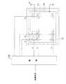
図1は、アクティブ駆動型のELディスプレイ装置の概略構成を示す図である。
図1に示す如く、かかるELディスプレイ装置は、表示パネル10と、この表示パネル10を映像信号に応じて駆動する駆動装置100とから構成される。
表示パネル10には、共通接地電極16、共通電源電極17、1画面のn個の水平走査ライン各々を担う走査ライン(走査電極)A1〜An、及び各走査ラインに交叉して配列されたm個のデータライン(データ電極)D1〜Dmが夫々形成されている。上記走査ラインA1〜An及びデータラインD1〜Dmの各交差部には、画素を担うアクティブ駆動型のELユニットE1,1〜En,mが形成されている。共通電源電極17にはELユニットEを駆動すべき電源電圧VAが印加されており、共通接地電極16は接地されている。
【0004】
図2は、1つの走査ラインA及びデータラインDの交差部に形成されているELユニットEの内部構成の一例を示す図である。
図2において、走査ライン選択用のFET(Field Effect Transistor)11のゲートには走査ラインAが接続され、そのドレインにはデータラインDが接続されている。FET11のソースには発光駆動用のFET12のゲートが接続されている。FET12のソースには共通電源電極17を介して電源電圧VAが印加されており、そのゲート及びソース間にはキャパシタ13が接続されている。更に、FET12のドレインにはEL素子15のアノード端が接続されている。EL素子15のカソード端は、共通接地電極16を介して接地されている。
【0005】
駆動装置100は、表示パネル10の走査ラインA1〜An各々に順次、択一的に走査パルスを印加して行く。更に、駆動装置100は、入力された映像信号に基づき、各水平走査ラインに対応した画素データ電圧DP1〜DPmを発生し、これらを上記走査パルスの印加タイミングに同期させてデータラインD1〜Dmに夫々印加する。この際、走査パルスの印加された走査ラインA上に接続されているELユニットの各々が画素データの書込対象となる。画素データの書込対象となったELユニットE内のFET11は、上記走査パルスに応じてオン状態となり、データラインDを介して供給された上記画素データ電圧DPをFET12のゲート及びキャパシタ13に夫々印加する。FET12は、かかる画素データ電圧DPが低電圧である場合に、上記電圧VAに基づいて生成した所定の発光駆動電流IdをEL素子15に供給する。EL素子15は、上記発光駆動電流Idに応じて所定の輝度で発光する。
【0006】
ところが、温度変化、経年変化等によりFET12のゲート・ソース間電圧−出力電流特性が変化すると、ゲート・ソース間電圧VGS(=電源電圧VA−ゲート電圧G)が固定であることから、出力電流、すなわち発光駆動電流Idが変動してEL素子15の輝度が変動してしまう。又、電源電圧VAは、EL素子15における温度変化、又は経年変化等による順方向電圧の増加分を見越して予め大きめに設定されているので、初期段階又は標準状態では無駄な電力消費が多かった。
【0007】
【発明が解決しようとする課題】
本発明は、かかる問題を解決せんとして為されたものであり、温度変化や経時変化に拘わらず、映像信号に対応した適切な輝度で画像表示を行うことが可能なディスプレイ装置を提供することにある。
【0008】
【課題を解決するための手段】
本発明によるディスプレイ装置は、制御端に印加される電圧に応じて駆動電流を発生する駆動トランジスタと、前記駆動電流に応じて発光する発光素子とからなる発光ユニットがマトリクス状に配列されてなる表示パネルを搭載したディスプレイ装置であって、基準電流を発生する電流源と、電源電圧が印加されるべき入力端、前記電流源が接続されている出力端、及び前記出力端に接続されている制御端を有しかつ前記駆動トランジスタと同一の電気的特性を有する基準トランジスタと、からなり前記基準トランジスタの前記制御端上の電圧を基準制御電圧として出力する基準制御電圧発生回路と、入力映像信号に基づく画素毎の画素データに応じて前記電源電圧及び前記基準制御電圧の内の一方を前記駆動トランジスタの前記制御端に供給するデータドライバと、を有する。
【0009】
【発明の実施の形態】
本発明の実施例を図面を参照しつつ詳細に説明する。
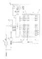
図3は、本発明によるアクティブマトリクス駆動型のELディスプレイ装置の構成を示す図である。
図3において、エレクトロルミネセンスディスプレイパネルとしての表示パネル10には、電源回路(図示せぬ)から供給された電源電圧VAが印加されている共通電源電極17、及び共通接地電極16が形成されている。又、かかる表示パネル10には、1画面のn個の水平走査ライン各々を担う走査ラインA1〜Anと、各走査ラインに交叉して配列された夫々m個の赤色駆動データラインDR1〜DRm、緑色駆動データラインDG1〜DGm、及び青色駆動データラインDB1〜DBmが形成されている。走査ラインA1〜Anと、赤色駆動データラインDR1〜DRmとの各交差部には、赤色発光を担うELユニットERが形成されている。又、走査ラインA1〜Anと、緑色駆動データラインDG1〜DGmとの各交差部には、緑色発光を担うELユニットEGが形成されている。更に、走査ラインA1〜Anと、青色駆動データラインDB1〜DBmとの各交差部には、青色発光を担うELユニットEBが形成されている。
【0010】
尚、ELユニットER、EG及びEBは共に図2に示す如き内部構成を有するものである。ただし、ELユニットERに設けられているEL素子15は赤色発光を為し、ELユニットEGに設けられているEL素子15は緑色発光を為し、ELユニットEBに設けられているEL素子15は青色発光を為す。
A/D変換器21は、入力された映像信号を画素毎に対応した画素データPDR、PDG、及びPDBに変換してメモリ22に供給する。尚、画素データPDRは、入力された映像信号における赤色成分を担う画素データである。又、画素データPDGは、入力された映像信号における緑色成分を担う画素データであり、画素データPDBは、青色成分を担う画素データである。
【0011】
駆動制御回路20は、入力された映像信号に応じて、走査ラインA1〜An各々に順次印加すべき走査パルスの印加タイミングを示すタイミング信号を生成し、これを走査ドライバ24に供給する。走査ドライバ24は、かかるタイミング信号に応じて、表示パネル10の走査ラインA1〜An各々に順次、走査パルスSPを印加して行く。
【0012】
又、駆動制御回路20は、上記画素データPDR、PDG、及びPDBをメモリ22に順次書き込むべき書込信号を生成してこれをメモリ22に供給する。更に、駆動制御回路20は、メモリ22に書き込まれた画素データPDR、PDG、及びPDBを夫々1ライン分ずつ読み出すべき読出信号を生成してこれをメモリ22に供給する。
【0013】
メモリ22は、駆動制御回路20から供給された書込信号に応じて、上記画素データPDR、PDG、及びPDBを順次書き込む。そして、1画面分の書き込みが終了すると、メモリ22は、画素データPDR、PDG及びPDBを夫々1ライン分ずつ読み出し、これらを画素データPDR1〜PDRm、PDG1〜PDGm、及びPDB1〜PDBmとして同時にデータドライバ23に供給する。
【0014】
データドライバ23は、上記画素データPDR1〜PDRm各々の論理レベルに対応した電圧を有する画素データ電圧DPR1〜DPRmを発生し、これらを表示パネル10の赤色駆動データラインDR1〜DRmに夫々印加する。又、データドライバ23は、上記画素データPDG1〜PDGm各々の論理レベルに対応した電圧を有する画素データ電圧DPG1〜DPGmを発生し、これらを表示パネル10の緑色駆動データラインDG1〜DGmに夫々印加する。更に、データドライバ23は、上記画素データPDB1〜PDBm各々の論理レベルに対応した電圧を有する画素データ電圧DPB1〜DPBmを発生し、これらを表示パネル10の青色駆動データラインDB1〜DBmに夫々印加する。
【0015】
ここで、前述した如き走査パルスSPの印加された走査ラインAに接続されているELユニットEが対象となって、各色毎のデータラインDを介して供給された画素データ電圧DPを取り込む。すなわち、この際、ELユニットE内のFET11は、上記走査パルスSPに応じてオン状態となり、各色毎のデータラインDを介して供給された上記画素データ電圧DPをFET12のゲート及びキャパシタ13に夫々印加する。FET12は、かかる画素データ電圧DPが所定の電圧値である場合に、電源回路(図示せぬ)から供給された電源電圧VAに基づく発光駆動電流IdをEL素子15に供給する。この際、EL素子15は、上記発光駆動電流Idに応じて発光する。つまり、ELユニットER内のEL素子15は赤色発光し、ELユニットEG内のEL素子15は緑色発光し、ELユニットEB内のEL素子15は青色発光するのである。
【0016】
尚、データドライバ23は、上記電源電圧VAと、基準ゲート電圧発生回路40から供給された基準ゲート電圧VGR、VGG及びVGBに基づいて、上記画素データ電圧DPR、DPG及びDPBを発生する。
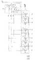
図4は、かかる基準ゲート電圧発生回路40、及びデータドライバ23の内部構成を示す図である。
【0017】
基準ゲート電圧発生回路40は、上記基準ゲート電圧VGRを生成する為のFET41R及び可変電流源42Rと、上記基準ゲート電圧VGGを生成する為のFET41G及び可変電流源42Gと、上記基準ゲート電圧VGBを生成する為のFET41B及び可変電流源42Bと、から構成される。
尚、上記FET41R、41G及び41Bのゲート・ソース間電圧−出力電流特性、ドレイン・ソース間電圧−出力電流特性、及びその他の電気的特性は、発光駆動用のFET12と略同一である。さらに好ましくは、上記FET41R、41G及び41Bは、FET12と略同一の材料を用い、かつ略同一のサイズ及び構造にて製造されたトランジスタである。つまり、FET41R、41G及び41Bは、発光駆動用のFET12と略同一仕様、更に好ましくは同一プロセスで製造されたトランジスタなのである。従って、FET41R、41G及び41Bと、FET12の温度変動特性及び経年変動特性が互いに同一となることが期待できる。
【0018】
FET41R、41G及び41B各々のソースには電源回路(図示せぬ)から供給された電源電圧VAが印加されている。FET41Rのドレインには、基準電流IREF-Rを流す可変電流源42Rが接続されており、そのドレインとゲートとは互いに接続されている。従って、FET41Rのゲートには、上記基準電流IREF-RがFET41Rのソース・ドレイン間に流れる際に必要となるゲート電圧が生じる。このゲート電圧が上記基準ゲート電圧VGRとして出力される。又、FET41Gのドレインには基準電流IREF-Gを流す可変電流源42Gが接続されており、そのドレインとゲートとは互いに接続されている。従って、FET41Gのゲートには、上記基準電流IREF-GがFET41Gのソース・ドレイン間に流れる際に必要となるゲート電圧が生じる。このゲート電圧が上記基準ゲート電圧VGGとして出力される。又、FET41Bのドレインには基準電流IREF-Bを流す可変電流源42Bが接続されており、そのドレインとゲートとは互いに接続されている。従って、FET41Bのゲートには、上記基準電流IREF-BがFET41Bのソース・ドレイン間に流れる際に必要となるゲート電圧が生じる。このゲート電圧が上記基準ゲート電圧VGBとして出力される。
【0019】
可変電流源42R、42G、及び42B各々は、表示パネル全体の輝度レベルを調整すべく駆動制御回路20から供給されたパネル輝度調整信号に対応した基準電流IREFを発生する。この際、上記基準電流IREFは、図2に示す如くELユニットE内に設けられているEL素子15に流すべき発光駆動電流と同一の電流である。尚、FET41R、41G、及び41BのトランジスタサイズがFET12と異なる場合には、上記基準電流IREFは上記発光駆動電流と等しくなくても良い。又、上記基準電流IREFをパネル外部から供給するようにしても良い。
【0020】
一方、データドライバ23は、スイッチング素子SR1〜SRm、スイッチング素子SG1〜SGm、及びスイッチング素子SB1〜SBmから構成される。
スイッチング素子SR1〜SRmは、夫々に対応して供給された画素データPDR1〜PDRm各々の論理レベルに応じて、電源回路から供給された電源電圧VA、及び基準ゲート電圧発生回路40から供給された基準ゲート電圧VGRの内の一方を選択的に表示パネル10の赤色駆動データラインDR1〜DRmに印加する。例えば、スイッチング素子SR1は、画素データPDR1が論理レベル1である場合には基準ゲート電圧VGRを赤色駆動データラインDR1に印加する一方、画素データPDR1が論理レベル0である場合には電源電圧VAを赤色駆動データラインDR1に印加する。これにより、上記電源電圧VAが選択された場合には電源電圧VAを有する画素データ電圧DPRが赤色駆動データラインDRに印加され、上記基準ゲート電圧VGRが選択された場合には基準ゲート電圧VGRを有する画素データ電圧DPRが赤色駆動データラインDRに印加されることになる。又、スイッチング素子SG1〜SGmは、夫々に対応して供給された画素データPDG1〜PDGm各々の論理レベルに応じて、電源回路から供給された電源電圧VA、及び基準ゲート電圧発生回路40から供給された基準ゲート電圧VGGの内の一方を選択的に表示パネル10の緑色駆動データラインDG1〜DGmに印加する。例えば、スイッチング素子SG1は、画素データPDG1が論理レベル1である場合には基準ゲート電圧VGGを緑色駆動データラインDG1に印加する一方、画素データPDG1が論理レベル0である場合には電源電圧VAを緑色駆動データラインDG1に印加する。これにより、上記電源電圧VAが選択された場合には電源電圧VAを有する画素データ電圧DPGが緑色駆動データラインDGに印加され、上記基準ゲート電圧VGGが選択された場合には基準ゲート電圧VGGを有する画素データ電圧DPGが緑色駆動データラインDGに印加されることになる。又、スイッチング素子SB1〜SBmは、夫々に対応して供給された画素データPDB1〜PDBm各々の論理レベルに応じて、電源回路から供給された電源電圧VA、及び基準ゲート電圧発生回路40から供給された基準ゲート電圧VGBの内の一方を選択的に表示パネル10の青色駆動データラインDB1〜DBmに印加する。例えば、スイッチング素子SB1は、画素データPDB1が論理レベル1である場合には基準ゲート電圧VGBを青色駆動データラインDB1に印加する一方、画素データPDB1が論理レベル0である場合には電源電圧VAを青色駆動データラインDB1に印加する。これにより、上記電源電圧VAが選択された場合には電源電圧VAを有する画素データ電圧DPBが青色駆動データラインDBに印加され、上記基準ゲート電圧VGBが選択された場合には基準ゲート電圧VGBを有する画素データ電圧DPBが青色駆動データラインDBに印加されることになる。尚、論理レベル0の際に供給される電源電圧VAの電圧値は、FET12をオフ状態に設定できる値である。
【0021】
ここで、図2に示す如きELユニットE内のFET12は、データラインD及びFET11を介してそのゲートに基準ゲート電圧(VGR、VGG、VGB)を有する画素データ電圧DPが供給されたら、このEL素子15を所定の輝度で発光させるべき発光駆動電流(IdR、IdG、IdB)をEL素子15に供給する。
この際、前述した如く、上記FET41R、41G及び41Bは、発光駆動用のFET12と同一仕様にて製造されたトランジスタである。よって、温度変化又は経年変化等により生じたFET12のゲート・ソース間電圧−出力電流特性の変動分は、そのままFET41R、41G及び41B各々のゲート・ソース間電圧−出力電流特性の変動にも表れる。又、上記基準電流(IREF-R、IREF-G、IREF-B)は、図2に示す如くELユニットE内に設けられているEL素子15を所定輝度で発光させる際に供給すべき発光駆動電流(IdR、IdG、IdB)と同一の電流である。
【0022】
従って、かかる構成によれば、常に、可変電流源(42R、42G、42B)にて生成された基準電流(IREF-R、IREF-G、IREF-B)と略同一電流の発光駆動電流(IdR、IdG、IdB)をEL素子15に供給し得る基準ゲート電圧(VGR、VGG、VGB)が生成されるようになる。これにより、温度変化又は経年変化等によるFET12のゲート・ソース間電圧−出力電流特性の変動に拘わらず、常に、一定輝度でEL素子を発光させることが可能となる。
【0023】
又、表示パネル全体の輝度調整を行う場合には、パネル輝度調整信号に応じて、基準ゲート電圧発生回路40に設けられている可変電流源(42R、42G、42B)は生成すべき基準電流(IREF-R、IREF-G、IREF-B)を変更する。この際、温度変化又は経年変化等によるFET12のゲート・ソース間電圧−出力電流特性の変動に拘わらず、表示パネル全体の輝度レベルをパネル輝度調整信号に対応した輝度レベルに調整することが可能となる。
【0024】
図5は、本発明の他の実施例によるアクティブマトリクス駆動型のELディスプレイ装置の構成を示す図である。
尚、図5に示されるELディスプレイ装置においては、図3に示されるELディスプレイ装置に搭載されている基準ゲート電圧発生回路40及び電源回路(図示せぬ)に代わり、可変電圧電源50及び順方向電圧モニタ回路51を搭載した点を除き、他の構成は図3に示されるものと同一である。よって、以下に、可変電圧電源50及び順方向電圧モニタ回路51の動作を中心に説明する。
【0025】
可変電圧電源50は、発光駆動用の電源電圧VAを発生し、これを表示パネル10の共通電源電極17、データドライバ23、及び順方向電圧モニタ回路51に供給する。又、可変電圧電源50は、基準ゲート電圧(VGR、VGG、及びVGB)を発生し、これらをデータドライバ23、及び順方向電圧モニタ回路51に供給する。
【0026】
図6は、順方向電圧モニタ回路51の内部構成を示す図である。
図6において、モニタ用FET(Field Effect Transistor)511Rのソースには可変電圧電源50から供給された電源電圧VAが印加されており、そのゲートには、基準ゲート電圧VGRが供給されている。モニタ用EL素子512Rは、赤色で発光するEL素子であり、そのカソードは接地されており、アノードにはモニタ用FET511Rのドレインが接続されている。かかるモニタ用EL素子512Rのアノードと、モニタ用FET511Rのドレインとの接続点に生じた電圧が、モニタ用EL素子512Rの順方向電圧VFRとして出力される。又、FET(Field Effect Transistor)511Gのソースには可変電圧電源50から供給された電源電圧VAが印加されており、そのゲートには、基準ゲート電圧VGGが供給されている。モニタ用EL素子512Gは、緑色で発光するEL素子であり、そのカソードは接地されており、アノードにはモニタ用FET511Gのドレインが接続されている。かかるモニタ用EL素子512Gのアノードと、モニタ用FET511Gのドレインとの接続点に生じた電圧が、モニタ用EL素子512Gの順方向電圧VFGとして出力される。又、FET(Field Effect Transistor)511Bのソースには可変電圧電源50から供給された電源電圧VAが印加されており、そのゲートには、基準ゲート電圧VGBが供給されている。モニタ用EL素子512Bは、青色で発光するEL素子であり、そのカソードは接地されており、アノードにはモニタ用FET511Bのドレインが接続されている。かかるモニタ用EL素子512Bのアノードと、モニタ用FET511Bのドレインとの接続点に生じた電圧が、モニタ用EL素子512Bの順方向電圧VFBとして出力される。
【0027】
尚、上記モニタ用FET511R、511G及び511Bのゲート・ソース間電圧−出力電流特性、ドレイン・ソース間電圧−出力電流特性、及びその他の電気的特性は、発光駆動用のFET12と略同一である。さらに好ましくは、上記モニタ用FET511R、511G及び511Bは、FET12と略同一の材料を用い、かつ略同一のサイズ及び構造にて製造されたトランジスタである。つまり、モニタ用FET511R、511G及び511Bは、発光駆動用のFET12と略同一仕様にて製造されたトランジスタなのである。従って、モニタ用FET511R、511G及び511Bと、FET12の温度変動特性及び経年変動特性が互いに同一となることが期待できる。
【0028】
更に、上記モニタ用EL素子512R、512G及び512Bの順方向電圧、及びその他の電気的特性はEL素子15と略同一である。さらに好ましくは、モニタ用EL素子512Rは、ELユニットER内に設けれているEL素子15と略同一の材料を用い、かつ略同一のサイズ及び構造にて製造されたEL素子である。又、モニタ用EL素子512Gは、ELユニットEG内に設けれているEL素子15と略同一の材料を用い、かつ略同一のサイズ及び構造にて製造されたEL素子である。又、モニタ用EL素子512Bは、ELユニットEB内に設けれているEL素子15と略同一の材料を用い、かつ略同一のサイズ及び構造にて製造されたEL素子である。つまり、モニタ用EL素子512R、512G及び512Bは、赤色発光を担うEL素子15、緑色発光を担うEL素子15、及び青色発光を担うEL素子15の各々と略同一仕様にて製造されたEL素子なのである。これにより、モニタ用EL素子512R、512G及び512Bと、EL素子15の温度変動特性及び経年変動特性が互いに同一となることが期待できる。
【0029】
以上の如き構成により、順方向電圧モニタ回路51は、基準ゲート電圧(VGR、VGG、及びVGB)にて発光駆動用のFET12を駆動した際に生じるであろう、EL素子15の順方向電圧を順方向電圧VFR、VFG、VFBとして得る。可変電圧電源50は、現在出力している電源電圧VAと、順方向電圧モニタ回路51から供給された順方向電圧VFRとの差分値が所定電圧値となるように、出力すべき電源電圧VA及び/又は基準ゲート電圧VGRを変更する。すなわち、ELユニットERに設けられているFET12のドレイン・ソース間電圧が、このFET12が安定して所定の発光駆動電流Idを供給し得る電圧値となるように、電源電圧VA及び/又は基準ゲート電圧VGRを変更するのである。又、可変電圧電源50は、現在出力している電源電圧VAと、順方向電圧モニタ回路51から供給された順方向電圧VFGとの差分値が所定電圧値となるように、出力すべき電源電圧VA及び/又は基準ゲート電圧VGGを変更する。すなわち、ELユニットEGに設けられているFET12のドレイン・ソース間電圧が、このFET12が安定して所定の発光駆動電流Idを供給し得る電圧値となるように、電源電圧VA及び/又は基準ゲート電圧VGGを変更するのである。更に、可変電圧電源50は、現在出力している電源電圧VAと、順方向電圧モニタ回路51から供給された順方向電圧VFBとの差分値が所定電圧値となるように、出力すべき電源電圧VA及び/又は基準ゲート電圧VGBを変更する。すなわち、ELユニットEBに設けられているFET12のドレイン・ソース間電圧が、このFET12が安定して所定の発光駆動電流Idを供給し得る電圧値となるように、電源電圧VA及び/又は基準ゲート電圧VGBを変更するのである。又、赤色発光駆動、青色発光駆動、及び緑色発光駆動各々で適切な電源電圧VAが異なる場合には、夫々別の電圧値に設定しても良いし、最も高い電圧値に設定しても良い。
【0030】
かかる構成によれば、発光駆動用のトランジスタであるFET12に供給すべき電源電圧VA及び/又は基準ゲート電圧VGが、常に、適切な発光駆動電流IdをEL素子に供給し得る電圧値に自動設定される。よって、温度変化又は経年変化等によるEL素子の順方向電圧の変動を考慮して、予め高めの電源電圧VAを固定供給する場合に比して、無駄な電力消費が削減される。
【0031】
尚、図5に示す実施例においては、可変電圧電源50にて電源電圧VAと共に基準ゲート電圧VGをも生成するようにしているが、この基準ゲート電圧VGに関しては図3に示す基準ゲート電圧発生回路40にて生成するようにしても良い。
図7は、かかる点に鑑みて為された本発明の他の実施例によるアクティブマトリクス駆動型のELディスプレイ装置の構成を示す図である。
【0032】
尚、図7に示されるELディスプレイ装置においては、表示パネル10、駆動制御回路20、A/D変換器21、メモリ22、データドライバ23、及び走査ドライバ24の各動作は図3又は図5に示されるものと同一であるので、その説明は省略する。
図7において、可変電圧電源50'は、発光駆動用の電源電圧VAを発生し、これを表示パネル10の共通電源電極17、データドライバ23、順方向電圧モニタ回路51及び基準ゲート電圧発生回路40に供給する。
【0033】
基準ゲート電圧発生回路40は、ELユニットER内のFET12が基準電流IREFと同一電流の発光駆動電流IdをEL素子15に供給する際に必要となるゲート電圧を発生し、これを基準ゲート電圧VGRとしてデータドライバ23及び順方向電圧モニタ回路51に供給する。又、基準ゲート電圧発生回路40は、ELユニットEG内のFET12が基準電流IREFと同一電流の発光駆動電流IdをEL素子15に供給する際に必要となるゲート電圧を発生し、これを基準ゲート電圧VGGとしてデータドライバ23及び順方向電圧モニタ回路51に供給する。更に、基準ゲート電圧発生回路40は、ELユニットEB内のFET12が基準電流IREFと同一電流の発光駆動電流IdをEL素子15に供給する際に必要となるゲート電圧を発生し、これを基準ゲート電圧VGBとしてデータドライバ23及び順方向電圧モニタ回路51に供給する。
【0034】
尚、基準ゲート電圧発生回路40は、図4に示す構成を有するものであり、その内部動作は前述したものと同一である。
一方、順方向電圧モニタ回路51は、図6に示す如き構成を有するものであり、その内部動作は前述したものと同一である。すなわち、順方向電圧モニタ回路51は、基準ゲート電圧発生回路40から供給された基準ゲート電圧(VGR、VGG、及びVGB)にて発光駆動用のFET12を駆動した際に生じるであろう、EL素子15の順方向電圧(VFR、VFG、VFB)を検出するのである。そして、順方向電圧モニタ回路51は、これら順方向電圧(VFR、VFG、VFB)を可変電圧電源50'に供給する。
【0035】
可変電圧電源50'は、現在出力している電源電圧VAと、順方向電圧モニタ回路51から供給された順方向電圧(VFR、VFG、VFB)各々との差分値が全て所定電圧値範囲内に収まるように、出力すべき電源電圧VAを変更する。すなわち、可変電圧電源50'は、ELユニットEに設けられているFET12のドレイン・ソース間電圧が、このFET12が安定して所定の発光駆動電流Idを供給し得る電圧値となるように、上記電源電圧VAを変更するのである。
【0036】
かかる構成によれば、発光駆動用のトランジスタであるFET12に供給すべき電源電圧VAが、常に、適切な発光駆動電流IdをEL素子に供給し得る電圧値に自動設定される。よって、温度変化又は経年変化等によるEL素子の順方向電圧の変動を考慮して予め高めの電源電圧VAを固定供給する場合に比して、無駄な電力消費が削減される。更に、電流源にて生成された基準電流と略同一電流の発光駆動電流IdをEL素子15に供給し得る基準ゲート電圧(VGR、VGG、VGB)が生成される。これにより、温度変化又は経年変化等によるFET12のゲート・ソース間電圧−出力電流特性の変動に拘わらず、常に、一定輝度でEL素子を発光させることが可能となる。
【0037】
【発明の効果】
以上の如く、本発明によるディスプレイ装置によれば、たとえ温度変化又は経年変化等の影響により発光駆動用のトランジスタ及びEL素子の特性が変動しても、電力消費を抑えつつ、常に一定の輝度でEL素子を発光させることが可能となる。
【図面の簡単な説明】
【図1】アクティブマトリクス駆動型のELディスプレイ装置の概略構成を示す図である。
【図2】各画素を担うELユニットEの内部構成の一例を示す図である。
【図3】本発明によるアクティブマトリクス駆動型のELディスプレイ装置の構成を示す図である。
【図4】基準ゲート電圧発生回路40及びデータドライバ23の内部構成を示す図である。
【図5】本発明の他の実施例によるELディスプレイ装置の構成を示す図である。
【図6】図5に示すELディスプレイ装置に搭載されている順方向電圧モニタ回路51の内部構成を示す図である。
【図7】本発明の他の実施例によるELディスプレイ装置の構成を示す図である。
【主要部分の符号の説明】
10 表示パネル
11,12,41R,41G,41B FET
15 EL素子
40 基準ゲート電圧発生回路
42R,42G,42B 可変電流源
50 可変電圧電源
51 順方向電圧モニタ回路[0001]
BACKGROUND OF THE INVENTION
The present invention relates to a display device equipped with an active matrix drive type display panel.
[0002]
[Prior art]
Currently, attention is focused on an electroluminescence display device (hereinafter referred to as an EL display device) on which a display panel using an organic electroluminescence element (hereinafter simply referred to as an EL element) is mounted as a light emitting element that bears a pixel. An active drive type is known as a display panel drive system using this EL display device.
[0003]
FIG. 1 is a diagram showing a schematic configuration of an active drive type EL display device.
As shown in FIG. 1, the EL display device includes a
The
[0004]
FIG. 2 is a diagram showing an example of the internal configuration of the EL unit E formed at the intersection of one scanning line A and data line D. As shown in FIG.
In FIG. 2, a scanning line A is connected to the gate of a FET (Field Effect Transistor) 11 for selecting a scanning line, and a data line D is connected to the drain thereof. The gate of the FET 12 for driving light emission is connected to the source of the FET 11. The source of the
[0005]
The
[0006]
However, if the gate-source voltage-output current characteristic of the
[0007]
[Problems to be solved by the invention]
The present invention has been made as a solution to such a problem, and provides a display device capable of displaying an image with appropriate luminance corresponding to a video signal regardless of a change in temperature or a change over time. is there.
[0008]
[Means for Solving the Problems]
A display device according to the present invention is a display in which light emitting units each including a driving transistor that generates a driving current according to a voltage applied to a control terminal and a light emitting element that emits light according to the driving current are arranged in a matrix. A display device equipped with a panel, a current source for generating a reference current, an input terminal to which a power supply voltage is to be applied, an output terminal to which the current source is connected, and a control connected to the output terminal A reference transistor having an end and having the same electrical characteristics as the driving transistor, a reference control voltage generating circuit for outputting a voltage on the control end of the reference transistor as a reference control voltage, and an input video signal One of the power supply voltage and the reference control voltage is supplied to the control terminal of the drive transistor according to pixel data for each pixel based on the pixel data. It has a data driver, a.
[0009]
DETAILED DESCRIPTION OF THE INVENTION
Embodiments of the present invention will be described in detail with reference to the drawings.
FIG. 3 is a diagram showing a configuration of an active matrix driving type EL display device according to the present invention.
In FIG. 3, a
[0010]
EL unit ER , EG And EB Both have an internal configuration as shown in FIG. However, EL unit ER The
The A /
[0011]
The
[0012]
Further, the
[0013]
The
[0014]
The
[0015]
Here, the EL unit E connected to the scanning line A to which the scanning pulse SP is applied as described above is targeted, and the pixel data voltage DP supplied via the data line D for each color is captured. That is, at this time, the FET 11 in the EL unit E is turned on in response to the scanning pulse SP, and the pixel data voltage DP supplied via the data line D for each color is supplied to the gate of the
[0016]
The
FIG. 4 is a diagram showing an internal configuration of the reference gate
[0017]
The reference gate
The gate-source voltage-output current characteristics, drain-source voltage-output current characteristics, and other electrical characteristics of the
[0018]
The source of each of the
[0019]
Each of the variable
[0020]
On the other hand, the
Switching element SR1 ~ SRm Is the pixel data PD supplied corresponding to eachR1 ~ PDRm According to each logic level, the power supply voltage V supplied from the power supply circuitA , And the reference gate voltage VG supplied from the reference gate
[0021]
Here, the
At this time, as described above, the
[0022]
Therefore, according to this configuration, the reference current (I) generated by the variable current source (42R, 42G, 42B) is always obtained.REF-R , IREF-G , IREF-B ) And the light emission drive current (IdR , IdG , IdB ) Can be supplied to the
[0023]
When the brightness of the entire display panel is adjusted, the variable current sources (42R, 42G, 42B) provided in the reference gate
[0024]
FIG. 5 is a diagram showing a configuration of an active matrix driving type EL display device according to another embodiment of the present invention.
In the EL display device shown in FIG. 5, instead of the reference gate
[0025]
The variable
[0026]
FIG. 6 is a diagram showing an internal configuration of the forward
In FIG. 6, a power supply voltage V supplied from a variable
[0027]
The gate-source voltage-output current characteristics, drain-source voltage-output current characteristics, and other electrical characteristics of the monitoring
[0028]
Further, the forward voltage and other electrical characteristics of the
[0029]
With the configuration as described above, the forward
[0030]
According to this configuration, the power supply voltage V to be supplied to the
[0031]
Note that in the embodiment shown in FIG.A At the same time, the reference gate voltage VG is also generated. However, the reference gate voltage VG may be generated by the reference gate
FIG. 7 is a diagram showing the configuration of an active matrix drive type EL display device according to another embodiment of the present invention made in view of the above points.
[0032]
In the EL display device shown in FIG. 7, the operations of the
In FIG. 7, a variable voltage power supply 50 'is a power supply voltage V for driving light emission.A Is supplied to the common
[0033]
The reference gate
[0034]
The reference gate
On the other hand, the forward
[0035]
The variable voltage power supply 50 'A Forward voltage (VF) supplied from the forward
[0036]
According to this configuration, the power supply voltage V to be supplied to the
[0037]
【The invention's effect】
As described above, according to the display device of the present invention, even when the characteristics of the light emission driving transistor and the EL element fluctuate due to the influence of temperature change or aging change, the power consumption is suppressed and the luminance is always constant. The EL element can emit light.
[Brief description of the drawings]
FIG. 1 is a diagram showing a schematic configuration of an active matrix drive type EL display device;
FIG. 2 is a diagram illustrating an example of an internal configuration of an EL unit E that handles each pixel.
FIG. 3 is a diagram showing a configuration of an active matrix driving type EL display device according to the present invention;
4 is a diagram showing an internal configuration of a reference gate
FIG. 5 is a diagram illustrating a configuration of an EL display device according to another embodiment of the present invention.
6 is a diagram showing an internal configuration of a forward
FIG. 7 is a diagram showing a configuration of an EL display device according to another embodiment of the present invention.
[Explanation of main part codes]
10 Display panel
11, 12, 41R, 41G, 41B FET
15 EL element
40 Reference gate voltage generator
42R, 42G, 42B Variable current source
50 Variable voltage power supply
51 Forward voltage monitor circuit
Claims (7)
Translated fromJapanese基準電流を発生する電流源と、電源電圧が印加されるべき入力端、前記電流源が接続されている出力端、及び前記出力端に接続されている制御端を有しかつ前記駆動トランジスタと同一の電気的特性を有する基準トランジスタと、からなり前記基準トランジスタの前記制御端上の電圧を基準制御電圧として出力する基準制御電圧発生回路と、
入力映像信号に基づく画素毎の画素データに応じて前記電源電圧及び前記基準制御電圧の内の一方を前記駆動トランジスタの前記制御端に供給するデータドライバと、を有することを特徴とするディスプレイ装置。A display device including a display panel in which light emitting units each including a driving transistor that generates a driving current according to a voltage applied to a control terminal and a light emitting element that emits light according to the driving current are arranged in a matrix. There,
A current source for generating a reference current; an input terminal to which a power supply voltage is to be applied; an output terminal to which the current source is connected; and a control terminal connected to the output terminal; A reference transistor having electrical characteristics, and a reference control voltage generation circuit that outputs a voltage on the control terminal of the reference transistor as a reference control voltage,
And a data driver that supplies one of the power supply voltage and the reference control voltage to the control terminal of the drive transistor in accordance with pixel data for each pixel based on an input video signal.
前記順方向電圧に応じて前記電源電圧を調整する可変電圧電源と、を更に備えたことを特徴とする請求項1記載のディスプレイ装置。A monitor light emitting element having the same electrical characteristics as the light emitting element, an input terminal to which a power supply voltage is to be applied, an output terminal to which the monitor light emitting element is connected, and the reference control voltage are applied. A monitor transistor having a control terminal and having the same electrical characteristics as the drive transistor, and a forward voltage monitor circuit that outputs a voltage on the output terminal of the monitor transistor as a forward voltage;
The display apparatus according to claim 1, further comprising: a variable voltage power supply that adjusts the power supply voltage in accordance with the forward voltage.
Priority Applications (4)
| Application Number | Priority Date | Filing Date | Title |
|---|---|---|---|
| JP2001360715AJP3852916B2 (en) | 2001-11-27 | 2001-11-27 | Display device |
| EP02026422AEP1318499B1 (en) | 2001-11-27 | 2002-11-26 | Display apparatus with active matrix type display panel |
| DE60224640TDE60224640T2 (en) | 2001-11-27 | 2002-11-26 | Display device with active matrix display panel |
| US10/304,854US7233302B2 (en) | 2001-11-27 | 2002-11-27 | Display apparatus with active matrix type display panel |
Applications Claiming Priority (1)
| Application Number | Priority Date | Filing Date | Title |
|---|---|---|---|
| JP2001360715AJP3852916B2 (en) | 2001-11-27 | 2001-11-27 | Display device |
Publications (2)
| Publication Number | Publication Date |
|---|---|
| JP2003162255A JP2003162255A (en) | 2003-06-06 |
| JP3852916B2true JP3852916B2 (en) | 2006-12-06 |
Family
ID=19171479
Family Applications (1)
| Application Number | Title | Priority Date | Filing Date |
|---|---|---|---|
| JP2001360715AExpired - Fee RelatedJP3852916B2 (en) | 2001-11-27 | 2001-11-27 | Display device |
Country Status (4)
| Country | Link |
|---|---|
| US (1) | US7233302B2 (en) |
| EP (1) | EP1318499B1 (en) |
| JP (1) | JP3852916B2 (en) |
| DE (1) | DE60224640T2 (en) |
Families Citing this family (50)
| Publication number | Priority date | Publication date | Assignee | Title |
|---|---|---|---|---|
| JP4423848B2 (en) | 2002-10-31 | 2010-03-03 | ソニー株式会社 | Image display device and color balance adjustment method thereof |
| JP4009238B2 (en)* | 2003-09-11 | 2007-11-14 | 松下電器産業株式会社 | Current drive device and display device |
| KR100658672B1 (en)* | 2003-11-27 | 2006-12-15 | 삼성에스디아이 주식회사 | Organic electroluminescent display and driving method thereof |
| US8421715B2 (en)* | 2004-05-21 | 2013-04-16 | Semiconductor Energy Laboratory Co., Ltd. | Display device, driving method thereof and electronic appliance |
| US7245297B2 (en) | 2004-05-22 | 2007-07-17 | Semiconductor Energy Laboratory Co., Ltd. | Display device and electronic device |
| JP2005345992A (en)* | 2004-06-07 | 2005-12-15 | Chi Mei Electronics Corp | Display device |
| JP4539963B2 (en)* | 2004-06-10 | 2010-09-08 | 東北パイオニア株式会社 | Active drive type light emitting display device and electronic device equipped with the display device |
| JP4896446B2 (en)* | 2004-06-29 | 2012-03-14 | 株式会社半導体エネルギー研究所 | Display device, driving method thereof, and electronic apparatus |
| US8013809B2 (en) | 2004-06-29 | 2011-09-06 | Semiconductor Energy Laboratory Co., Ltd. | Display device and driving method of the same, and electronic apparatus |
| JP4539967B2 (en)* | 2004-08-03 | 2010-09-08 | 東北パイオニア株式会社 | Luminescent panel drive device |
| JP4948754B2 (en)* | 2004-08-04 | 2012-06-06 | 株式会社 日立ディスプレイズ | Electroluminescence display device |
| US7540978B2 (en) | 2004-08-05 | 2009-06-02 | Novaled Ag | Use of an organic matrix material for producing an organic semiconductor material, organic semiconductor material and electronic component |
| DE112005002603A5 (en) | 2004-08-13 | 2007-08-09 | Novaled Gmbh | Layer arrangement for a light-emitting component |
| JP4822387B2 (en)* | 2004-08-31 | 2011-11-24 | 東北パイオニア株式会社 | Drive device for organic EL panel |
| DE102004045871B4 (en)* | 2004-09-20 | 2006-11-23 | Novaled Gmbh | Method and circuit arrangement for aging compensation of organic light emitting diodes |
| EP1648042B1 (en) | 2004-10-07 | 2007-05-02 | Novaled AG | A method for doping a semiconductor material with cesium |
| JP2006251011A (en)* | 2005-03-08 | 2006-09-21 | Tohoku Pioneer Corp | Driving apparatus and driving method of light emitting display panel |
| JP4803637B2 (en)* | 2005-03-08 | 2011-10-26 | 東北パイオニア株式会社 | Driving device and driving method for active matrix light emitting display panel |
| JP4753351B2 (en)* | 2005-03-15 | 2011-08-24 | 東北パイオニア株式会社 | Driving device for light emitting display panel and driving method thereof |
| EP1705727B1 (en) | 2005-03-15 | 2007-12-26 | Novaled AG | Light emitting element |
| JP4749010B2 (en)* | 2005-03-17 | 2011-08-17 | 東北パイオニア株式会社 | Driving device and driving method for active matrix light emitting display panel |
| JP4707090B2 (en)* | 2005-03-28 | 2011-06-22 | 東北パイオニア株式会社 | Driving device for light emitting display panel |
| EP1729280B1 (en) | 2005-03-31 | 2013-10-30 | Semiconductor Energy Laboratory Co., Ltd. | Display device, display module, electronic apparatus and driving method of the display device |
| EP2264806B1 (en) | 2005-04-13 | 2019-03-27 | Novaled GmbH | Assembly for an organic pin-type LED and manufacturing method |
| JP4811849B2 (en)* | 2005-05-19 | 2011-11-09 | 東北パイオニア株式会社 | Driving device and driving method of light emitting display panel |
| EP1727221B1 (en) | 2005-05-27 | 2010-04-14 | Novaled AG | Transparent organic light emitting diode |
| JP2006337456A (en)* | 2005-05-31 | 2006-12-14 | Tohoku Pioneer Corp | Light emitting device and checking method therefor |
| KR101139527B1 (en)* | 2005-06-27 | 2012-05-02 | 엘지디스플레이 주식회사 | Oled |
| JP4483725B2 (en)* | 2005-07-04 | 2010-06-16 | セイコーエプソン株式会社 | LIGHT EMITTING DEVICE, ITS DRIVE CIRCUIT, AND ELECTRONIC DEVICE |
| JP5020484B2 (en)* | 2005-07-12 | 2012-09-05 | 東北パイオニア株式会社 | Self-luminous display device and driving method thereof |
| JP5084003B2 (en)* | 2005-10-28 | 2012-11-28 | 東北パイオニア株式会社 | Driving device and driving method of light emitting display panel |
| EP1806795B1 (en) | 2005-12-21 | 2008-07-09 | Novaled AG | Organic Device |
| EP1804309B1 (en) | 2005-12-23 | 2008-07-23 | Novaled AG | Electronic device with a layer structure of organic layers |
| US7995012B2 (en)* | 2005-12-27 | 2011-08-09 | Semiconductor Energy Laboratory Co., Ltd. | Light emitting device |
| KR20070072142A (en)* | 2005-12-30 | 2007-07-04 | 엘지.필립스 엘시디 주식회사 | EL display device and driving method |
| EP1808909A1 (en) | 2006-01-11 | 2007-07-18 | Novaled AG | Electroluminescent light-emitting device |
| EP1848049B1 (en) | 2006-04-19 | 2009-12-09 | Novaled AG | Light emitting device |
| GB2441354B (en)* | 2006-08-31 | 2009-07-29 | Cambridge Display Tech Ltd | Display drive systems |
| US7928936B2 (en)* | 2006-11-28 | 2011-04-19 | Global Oled Technology Llc | Active matrix display compensating method |
| DE102007019260B4 (en) | 2007-04-17 | 2020-01-16 | Novaled Gmbh | Non-volatile organic storage element |
| JP2008268671A (en)* | 2007-04-23 | 2008-11-06 | Canon Inc | Liquid crystal display device, control method thereof, and liquid crystal projector system |
| DE102008036062B4 (en) | 2008-08-04 | 2015-11-12 | Novaled Ag | Organic field effect transistor |
| DE102008036063B4 (en) | 2008-08-04 | 2017-08-31 | Novaled Gmbh | Organic field effect transistor |
| JP2009042788A (en)* | 2008-11-10 | 2009-02-26 | Sony Corp | Display device and driving method thereof |
| US20100277400A1 (en)* | 2009-05-01 | 2010-11-04 | Leadis Technology, Inc. | Correction of aging in amoled display |
| US10319307B2 (en)* | 2009-06-16 | 2019-06-11 | Ignis Innovation Inc. | Display system with compensation techniques and/or shared level resources |
| US10796622B2 (en)* | 2009-06-16 | 2020-10-06 | Ignis Innovation Inc. | Display system with compensation techniques and/or shared level resources |
| JP2011118301A (en)* | 2009-12-07 | 2011-06-16 | Sony Corp | Display device, method for driving the same, and electronic equipment |
| DE102019105249B4 (en)* | 2019-03-01 | 2020-11-05 | Infineon Technologies Ag | INTEGRATED CIRCUIT |
| KR102831078B1 (en)* | 2021-02-09 | 2025-07-09 | 삼성디스플레이 주식회사 | Display device |
Family Cites Families (9)
| Publication number | Priority date | Publication date | Assignee | Title |
|---|---|---|---|---|
| US5719589A (en)* | 1996-01-11 | 1998-02-17 | Motorola, Inc. | Organic light emitting diode array drive apparatus |
| US6518962B2 (en)* | 1997-03-12 | 2003-02-11 | Seiko Epson Corporation | Pixel circuit display apparatus and electronic apparatus equipped with current driving type light-emitting device |
| US5903246A (en)* | 1997-04-04 | 1999-05-11 | Sarnoff Corporation | Circuit and method for driving an organic light emitting diode (O-LED) display |
| JP3049061B1 (en)* | 1999-02-26 | 2000-06-05 | キヤノン株式会社 | Image display device and image display method |
| JP4081852B2 (en)* | 1998-04-30 | 2008-04-30 | ソニー株式会社 | Matrix driving method for organic EL element and matrix driving apparatus for organic EL element |
| EP1130565A4 (en)* | 1999-07-14 | 2006-10-04 | Sony Corp | Current drive circuit and display comprising the same, pixel circuit, and drive method |
| EP1158483A3 (en)* | 2000-05-24 | 2003-02-05 | Eastman Kodak Company | Solid-state display with reference pixel |
| JP3437152B2 (en)* | 2000-07-28 | 2003-08-18 | ウインテスト株式会社 | Apparatus and method for evaluating organic EL display |
| TW569016B (en)* | 2001-01-29 | 2004-01-01 | Semiconductor Energy Lab | Light emitting device |
- 2001
- 2001-11-27JPJP2001360715Apatent/JP3852916B2/ennot_activeExpired - Fee Related
- 2002
- 2002-11-26DEDE60224640Tpatent/DE60224640T2/ennot_activeExpired - Lifetime
- 2002-11-26EPEP02026422Apatent/EP1318499B1/ennot_activeExpired - Lifetime
- 2002-11-27USUS10/304,854patent/US7233302B2/ennot_activeExpired - Lifetime
Also Published As
| Publication number | Publication date |
|---|---|
| DE60224640T2 (en) | 2008-05-21 |
| JP2003162255A (en) | 2003-06-06 |
| EP1318499A2 (en) | 2003-06-11 |
| DE60224640D1 (en) | 2008-03-06 |
| US20030128201A1 (en) | 2003-07-10 |
| EP1318499A3 (en) | 2003-08-27 |
| US7233302B2 (en) | 2007-06-19 |
| EP1318499B1 (en) | 2008-01-16 |
Similar Documents
| Publication | Publication Date | Title |
|---|---|---|
| JP3852916B2 (en) | Display device | |
| KR100442731B1 (en) | Display apparatus with luminance adjustment function | |
| US6479940B1 (en) | Active matrix display apparatus | |
| CN101465097B (en) | Self-luminous display device and driving method of the same | |
| KR101738920B1 (en) | Organic Light Emitting Display Device | |
| KR101374443B1 (en) | Organic Light Emitting Diode Display | |
| CN101086818A (en) | Image display device | |
| KR102636682B1 (en) | Display device and driving method therof | |
| US8605066B2 (en) | Display apparatus including display pixels and light detection units, method for controlling light detection operation | |
| CN101359449A (en) | Organic light emitting display and driving method thereof | |
| CN113053321B (en) | Organic light emitting display device and driving method thereof | |
| KR20040042846A (en) | Display device | |
| WO2015172411A1 (en) | Panel drive circuit and panel drive method | |
| JP2009031710A (en) | Organic electroluminescent display device and driving method thereof | |
| KR20150004554A (en) | Pixel and organic light emitting display device using the same | |
| US20210035493A1 (en) | Display device | |
| CN110634442A (en) | OLED display device and driving method thereof | |
| CN101577088B (en) | Organic light emitting display and method for driving the same | |
| JP2003043999A (en) | Display pixel circuit and self-luminous display device | |
| KR20140140814A (en) | Organic Light Emitting Display Device | |
| US20110084992A1 (en) | Active matrix display apparatus | |
| JP2003108073A (en) | Self-luminous display | |
| KR20140054758A (en) | Organic light emitting display device and driving method thereof | |
| JP2009520226A (en) | Method for controlling a display panel by capacitive coupling | |
| EP1528533A2 (en) | Method for driving electro-optical device, electro-optical device and electronic equipment |
Legal Events
| Date | Code | Title | Description |
|---|---|---|---|
| A621 | Written request for application examination | Free format text:JAPANESE INTERMEDIATE CODE: A621 Effective date:20041125 | |
| A977 | Report on retrieval | Free format text:JAPANESE INTERMEDIATE CODE: A971007 Effective date:20060830 | |
| TRDD | Decision of grant or rejection written | ||
| A01 | Written decision to grant a patent or to grant a registration (utility model) | Free format text:JAPANESE INTERMEDIATE CODE: A01 Effective date:20060904 | |
| A61 | First payment of annual fees (during grant procedure) | Free format text:JAPANESE INTERMEDIATE CODE: A61 Effective date:20060904 | |
| R150 | Certificate of patent or registration of utility model | Ref document number:3852916 Country of ref document:JP Free format text:JAPANESE INTERMEDIATE CODE: R150 Free format text:JAPANESE INTERMEDIATE CODE: R150 | |
| FPAY | Renewal fee payment (event date is renewal date of database) | Free format text:PAYMENT UNTIL: 20100915 Year of fee payment:4 | |
| FPAY | Renewal fee payment (event date is renewal date of database) | Free format text:PAYMENT UNTIL: 20100915 Year of fee payment:4 | |
| FPAY | Renewal fee payment (event date is renewal date of database) | Free format text:PAYMENT UNTIL: 20110915 Year of fee payment:5 | |
| FPAY | Renewal fee payment (event date is renewal date of database) | Free format text:PAYMENT UNTIL: 20120915 Year of fee payment:6 | |
| FPAY | Renewal fee payment (event date is renewal date of database) | Free format text:PAYMENT UNTIL: 20120915 Year of fee payment:6 | |
| FPAY | Renewal fee payment (event date is renewal date of database) | Free format text:PAYMENT UNTIL: 20130915 Year of fee payment:7 | |
| LAPS | Cancellation because of no payment of annual fees |