JP3850712B2 - Multilayer semiconductor device - Google Patents
Multilayer semiconductor deviceDownload PDFInfo
- Publication number
- JP3850712B2 JP3850712B2JP2001331181AJP2001331181AJP3850712B2JP 3850712 B2JP3850712 B2JP 3850712B2JP 2001331181 AJP2001331181 AJP 2001331181AJP 2001331181 AJP2001331181 AJP 2001331181AJP 3850712 B2JP3850712 B2JP 3850712B2
- Authority
- JP
- Japan
- Prior art keywords
- semiconductor device
- semiconductor
- stacked
- lowermost
- land portion
- Prior art date
- Legal status (The legal status is an assumption and is not a legal conclusion. Google has not performed a legal analysis and makes no representation as to the accuracy of the status listed.)
- Expired - Fee Related
Links
Images


Classifications
- H—ELECTRICITY
- H01—ELECTRIC ELEMENTS
- H01L—SEMICONDUCTOR DEVICES NOT COVERED BY CLASS H10
- H01L25/00—Assemblies consisting of a plurality of semiconductor or other solid state devices
- H01L25/03—Assemblies consisting of a plurality of semiconductor or other solid state devices all the devices being of a type provided for in a single subclass of subclasses H10B, H10D, H10F, H10H, H10K or H10N, e.g. assemblies of rectifier diodes
- H01L25/10—Assemblies consisting of a plurality of semiconductor or other solid state devices all the devices being of a type provided for in a single subclass of subclasses H10B, H10D, H10F, H10H, H10K or H10N, e.g. assemblies of rectifier diodes the devices having separate containers
- H01L25/105—Assemblies consisting of a plurality of semiconductor or other solid state devices all the devices being of a type provided for in a single subclass of subclasses H10B, H10D, H10F, H10H, H10K or H10N, e.g. assemblies of rectifier diodes the devices having separate containers the devices being integrated devices of class H10
- H—ELECTRICITY
- H01—ELECTRIC ELEMENTS
- H01L—SEMICONDUCTOR DEVICES NOT COVERED BY CLASS H10
- H01L2224/00—Indexing scheme for arrangements for connecting or disconnecting semiconductor or solid-state bodies and methods related thereto as covered by H01L24/00
- H01L2224/01—Means for bonding being attached to, or being formed on, the surface to be connected, e.g. chip-to-package, die-attach, "first-level" interconnects; Manufacturing methods related thereto
- H01L2224/42—Wire connectors; Manufacturing methods related thereto
- H01L2224/44—Structure, shape, material or disposition of the wire connectors prior to the connecting process
- H01L2224/45—Structure, shape, material or disposition of the wire connectors prior to the connecting process of an individual wire connector
- H01L2224/45001—Core members of the connector
- H01L2224/45099—Material
- H01L2224/451—Material with a principal constituent of the material being a metal or a metalloid, e.g. boron (B), silicon (Si), germanium (Ge), arsenic (As), antimony (Sb), tellurium (Te) and polonium (Po), and alloys thereof
- H01L2224/45138—Material with a principal constituent of the material being a metal or a metalloid, e.g. boron (B), silicon (Si), germanium (Ge), arsenic (As), antimony (Sb), tellurium (Te) and polonium (Po), and alloys thereof the principal constituent melting at a temperature of greater than or equal to 950°C and less than 1550°C
- H01L2224/45144—Gold (Au) as principal constituent
- H—ELECTRICITY
- H01—ELECTRIC ELEMENTS
- H01L—SEMICONDUCTOR DEVICES NOT COVERED BY CLASS H10
- H01L2224/00—Indexing scheme for arrangements for connecting or disconnecting semiconductor or solid-state bodies and methods related thereto as covered by H01L24/00
- H01L2224/01—Means for bonding being attached to, or being formed on, the surface to be connected, e.g. chip-to-package, die-attach, "first-level" interconnects; Manufacturing methods related thereto
- H01L2224/42—Wire connectors; Manufacturing methods related thereto
- H01L2224/47—Structure, shape, material or disposition of the wire connectors after the connecting process
- H01L2224/48—Structure, shape, material or disposition of the wire connectors after the connecting process of an individual wire connector
- H01L2224/481—Disposition
- H01L2224/48151—Connecting between a semiconductor or solid-state body and an item not being a semiconductor or solid-state body, e.g. chip-to-substrate, chip-to-passive
- H01L2224/48221—Connecting between a semiconductor or solid-state body and an item not being a semiconductor or solid-state body, e.g. chip-to-substrate, chip-to-passive the body and the item being stacked
- H01L2224/48225—Connecting between a semiconductor or solid-state body and an item not being a semiconductor or solid-state body, e.g. chip-to-substrate, chip-to-passive the body and the item being stacked the item being non-metallic, e.g. insulating substrate with or without metallisation
- H01L2224/4824—Connecting between the body and an opposite side of the item with respect to the body
- H—ELECTRICITY
- H01—ELECTRIC ELEMENTS
- H01L—SEMICONDUCTOR DEVICES NOT COVERED BY CLASS H10
- H01L2924/00—Indexing scheme for arrangements or methods for connecting or disconnecting semiconductor or solid-state bodies as covered by H01L24/00
- H01L2924/15—Details of package parts other than the semiconductor or other solid state devices to be connected
- H01L2924/151—Die mounting substrate
- H01L2924/153—Connection portion
- H01L2924/1531—Connection portion the connection portion being formed only on the surface of the substrate opposite to the die mounting surface
- H01L2924/15311—Connection portion the connection portion being formed only on the surface of the substrate opposite to the die mounting surface being a ball array, e.g. BGA
- H—ELECTRICITY
- H01—ELECTRIC ELEMENTS
- H01L—SEMICONDUCTOR DEVICES NOT COVERED BY CLASS H10
- H01L2924/00—Indexing scheme for arrangements or methods for connecting or disconnecting semiconductor or solid-state bodies as covered by H01L24/00
- H01L2924/15—Details of package parts other than the semiconductor or other solid state devices to be connected
- H01L2924/151—Die mounting substrate
- H01L2924/153—Connection portion
- H01L2924/1532—Connection portion the connection portion being formed on the die mounting surface of the substrate
- H01L2924/15321—Connection portion the connection portion being formed on the die mounting surface of the substrate being a ball array, e.g. BGA
- H—ELECTRICITY
- H01—ELECTRIC ELEMENTS
- H01L—SEMICONDUCTOR DEVICES NOT COVERED BY CLASS H10
- H01L2924/00—Indexing scheme for arrangements or methods for connecting or disconnecting semiconductor or solid-state bodies as covered by H01L24/00
- H01L2924/15—Details of package parts other than the semiconductor or other solid state devices to be connected
- H01L2924/151—Die mounting substrate
- H01L2924/153—Connection portion
- H01L2924/1532—Connection portion the connection portion being formed on the die mounting surface of the substrate
- H01L2924/1533—Connection portion the connection portion being formed on the die mounting surface of the substrate the connection portion being formed both on the die mounting surface of the substrate and outside the die mounting surface of the substrate
- H01L2924/15331—Connection portion the connection portion being formed on the die mounting surface of the substrate the connection portion being formed both on the die mounting surface of the substrate and outside the die mounting surface of the substrate being a ball array, e.g. BGA
Landscapes
- Engineering & Computer Science (AREA)
- Power Engineering (AREA)
- Microelectronics & Electronic Packaging (AREA)
- Physics & Mathematics (AREA)
- Condensed Matter Physics & Semiconductors (AREA)
- General Physics & Mathematics (AREA)
- Computer Hardware Design (AREA)
- Wire Bonding (AREA)
Description
Translated fromJapanese【0001】
【発明の属する技術分野】
本発明は、半導体チップを有する半導体装置を複数個積層することにより、高機能化、小型化及び薄型化を図るための積層型半導体装置に関するものである。
【0002】
【従来の技術】
近年、電子機器の小型化の要求に対応するものとして、また、組立工程の自動化に適合するものとして、QFP(Quad Flat Package)型やBGA(Ball Grid
Allay)型のCSP(Chip Size Package)式半導体装置が広く用いられている。
【0003】
これらの半導体装置においては、実装効率を高めるために、半導体装置としてのフィルムキャリア半導体モジュールを複数積み重ねて、電気的に接続したマルチチップ半導体装置が例えば特開平10−163414号公報に開示されている。
【0004】
上記のマルチチップ半導体装置は、図11に示すように、フィルムキャリア半導体モジュール88a・88b・88c・88dが下から順に積層されてなっており、各フィルムキャリア半導体モジュール88a・88b・88c・88dの間には各両端にスペーサ90a・90b・90c・90dが介装されている。上記各スペーサ90a・90b・90c・90dには表面パターン92aと裏面パターン94aとが形成されており、その両表面パターン92a及び裏面パターン94aはスルーホール96aに充填された導電性材料にて電気的につながっている。
【0005】
上記フィルムキャリア半導体モジュール88aには、半導体チップ72aにバンプ74a…が形成されている。これらバンプ74a…はフィルムキャリアテープ76aのインナーリード部80aと電気的に接続される。また、これらフィルムキャリア半導体モジュール88aの電気接続部分についての露出を防止するために、半導体チップ72aの上面及びインナーリード部80aを含む半導体チップ72aの側部には保護コート樹脂84aがコートしてある。
【0006】
上記フィルムキャリアテープ76aは半導体チップ72aの外側に張り出しており、その外側端部にアウターリード部82aを有している。そして、このアウターリード部82aは、上記スペーサ90aの表面パターン92a及び裏面パターン94aに電気的につながっている。したがって、フィルムキャリア半導体モジュール88a・88b・88c・88dの共通信号は、上から下まで同心に設けられた上記部材からなる共通接続端子によって、最下段のフィルムキャリア半導体モジュール88aの底面から外部に出力されるようになっている。
【0007】
なお、上記の説明においては、図11に示す最下段のフィルムキャリア半導体モジュール88aの構成について説明したが、下から第2段目、第3段目、第4段目のフィルムキャリア半導体モジュール88b・88c・88dも同様の構成である。
【0008】
ここで、上記の互いに隣り合う例えばフィルムキャリア半導体モジュール88a・88b間を電気的に接続するための構成を詳述する。
【0009】
先ず、フィルムキャリア半導体モジュール88bの接続位置における裏面パターン94bに半田ボールを設け、この半田ボールに対面する位置におけるフィルムキャリア半導体モジュール88aのアウターリード部82aと該半田ボールとを当接させる。次いで、フィルムキャリア半導体モジュール88a・88bを、それらの厚さ方向にて押圧しながら、半田ボールが軟化する温度に加熱することにより接続層78bが形成される。この結果、この接続層78bによって、上記例えばフィルムキャリア半導体モジュール88a・88b間が電気的に接続されるものとなっている。同様にして、フィルムキャリア半導体モジュール88b・88c・88d間を接続する。これにより、BGA型のCSP式積層型半導体装置が完成される。
【0010】
【発明が解決しようとする課題】
ところで、上記従来の積層型半導体装置では、上下間の電気的導通をとる場合、同一信号端子は同じ端子位置にて上下間の電気的導通を確保している。すなわち、この種の積層型半導体装置では、上下のパッケージ間の接続用端子は半導体チップの外側に配列する必要がある。
【0011】
ここで、メモリデバイス等の半導体チップサイズが大きい半導体装置ではパッケージ外形サイズつまりパッケージ実装面積が、メモリデバイス等の半導体装置以外のパッケージサイズに比べて大きくなる傾向がある。
【0012】
したがって、上記従来の積層型半導体装置では、上記のメモリデバイスとは別の機能を持つ半導体装置を上記複数個のメモリデバイスの半導体装置と一緒に積層する場合には、次の問題が生じる。
【0013】
すなわち、メモリデバイスとは別の機能を持つ半導体装置は該メモリデバイスの半導体装置と大きさが異なるので、上述したように、半導体装置の外側部分で同心上に揃えて電気的接続をとるということができない。この結果、メモリデバイスとは別の機能を持つ半導体装置を別の部分に実装しなければならないので、実装基板が大きくなり、携帯機器等の小型化が要求される機器に対する要求を満たすことができないという問題点を有している。
【0014】
本発明は、上記従来の問題点に鑑みなされたものであって、その目的は、サイズの異なる半導体装置であっても、最大の大きさを有する半導体装置領域の範囲内で多段に積層して電気的接続を可能とする積層型半導体装置を提供することにある。
【0015】
【課題を解決するための手段】
本発明の積層型半導体装置は、上記課題を解決するために、複数個の半導体装置を積層した積層型半導体装置において、上記複数個の半導体装置のうちの最下段の半導体装置を除く上段側の半導体装置に対して上下間で共通して電気的導通を確保して外部出力するための第1共通接続端子が、全ての半導体装置の端部側の一部の領域における同心位置にそれぞれ配設されるとともに、上記複数個の半導体装置のうちの最下段の半導体装置から外部出力するための一部の外部出力端子である第2接続端子は、上記最下段の半導体装置の第1共通接続端子よりも内側に配設されているとともに、上記最下段の半導体装置における上記第2接続端子とは異なる他の外部出力端子は、上記最下段を除く上段側の半導体装置と共通に外部出力するための接続端子として、上記端部側における第1共通接続端子が配設された領域以外の他の領域に配設されていることを特徴としている。なお、半導体装置の上下関係は、表面側又は裏面側のいずれが上下であるかを問わない。すなわち、半導体装置の上下関係は相対的なものであり、最上段に他の半導体装置とは異なる種類の半導体装置を積層することも可能である。
【0016】
先ず、例えば、メモリデバイス等の半導体装置は、半導体チップの面積が大きいので、その外側に外部接続用の端子が配置される。したがって、同一のメモリデバイス等の半導体装置を複数個積層する場合には、共通信号線として、外部接続用の端子を同心上で接続することによって容易に最下段の半導体装置の外部接続用の端子から共通の出力信号を取り出すことができる。
【0017】
しかしながら、複数個のメモリデバイス等の半導体装置と、これらとは異なる機能を有する半導体装置とを一緒に積層する場合には、一般に、メモリデバイスとは異なる機能を有する半導体装置の半導体チップはサイズが小さいので、一緒には積層することができない。つまり、共通の出力信号を取り出すことが困難である。
【0018】
そこで、本発明では、先ず、複数個の半導体装置のうちの最下段の半導体装置を除く上段側の半導体装置に対して上下間で共通して電気的導通を確保して外部出力するための第1共通接続端子は、全ての半導体装置の端部側の同心位置にそれぞれ配設される。したがって、最下段の半導体装置にも、上段側の複数個の半導体装置の電気信号を実装基板に伝えるための第1共通接続端子が設けられる。すなわち、本発明では、最下段の半導体装置に設けられた第1共通接続端子は、上段側の半導体装置からの出力を外部へ出力するための積層用端子として機能するものとなっている。
【0019】
一方、最下段の半導体装置における外部出力するための第2接続端子は、最下段の半導体装置の第1共通接続端子よりも内側に配設されている。したがって、最下段の半導体装置においては、この内側に配設された第2接続端子から外部へ出力することが可能となる。
【0020】
この結果、1個の半導体装置の半導体チップサイズが他の半導体装置の半導体チップサイズよりも小さい場合であっても、半導体チップサイズの小さい半導体装置を最下段にして積層しかつ上述のように第1共通接続端子及び第2接続端子を形成することによって、上段側の半導体装置の実装面積を拡大することなく半導体チップサイズの小さい半導体装置を積層することができる。
【0021】
したがって、サイズの異なる半導体装置であっても、最大の大きさを有する半導体装置領域の範囲内で多段に積層して電気的接続を可能とする積層型半導体装置を提供することができる。
【0022】
また、本発明の積層型半導体装置は、上記の積層型半導体装置において、上段側に設けられた半導体装置と、最下段の半導体装置又は最下段から連続して積層される半導体装置とは機能が異なることを特徴としている。
【0023】
上記の発明によれば、上段側に設けられた半導体装置と、最下段の半導体装置又は最下段から連続して積層される半導体装置とは機能が異なるので、例えば、上段側の半導体装置がメモリデバイス機能を有する一方、最下段の半導体装置が液晶コントローラデバイス機能を有するという場合にも、上段側の半導体装置の実装面積を拡大することなく半導体チップサイズの小さい複数個の半導体装置を積層することができる。
【0024】
また、本発明の積層型半導体装置は、上記の積層型半導体装置において、最下段の半導体装置に備えられたチップサイズよりも大きい半導体チップを備える半導体装置を上段側に含むことを特徴としている。
【0025】
この結果、例えば、メモリデバイス機能を有する半導体装置と他の機能を有する半導体装置とを積層する場合のように、サイズの異なる複数個の半導体装置であっても、最大の大きさを有する例えばメモリデバイス機能を有する半導体装置領域の範囲内で多段に積層して電気的接続を可能とする積層型半導体装置を提供することができる。
【0026】
また、本発明の積層型半導体装置は、上記の積層型半導体装置において、複数個の半導体装置のうちのいずれかは、1個の半導体装置に複数個の半導体チップを搭載したものからなっていることを特徴としている。
【0027】
上記の発明によれば、複数個の半導体装置のうちのいずれかは、1個の半導体装置に複数個の半導体チップを搭載したものからなっているので、例えばフラッシュメモリのメモリ容量を増やすために1個の半導体装置に2個の半導体チップを形成した場合においても、最大の大きさを有する半導体装置領域の範囲内で多段に積層して電気的接続を可能とする積層型半導体装置を提供することができる。
【0028】
【発明の実施の形態】
〔実施の形態1〕
本発明の実施の一形態について図1ないし図7に基づいて説明すれば、以下の通りである。
【0029】
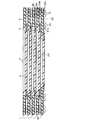
本実施の形態の積層型半導体装置は、図1に示すように、半導体チップサイズの大きい半導体装置1…が上側4段に積層されているとともに、最下段には半導体チップサイズの小さい半導体装置20が1個設けられている。したがって、5段の積層型半導体装置となっている。ただし、必ずしも5段に限らず、他の複数段であってよい。
【0030】
上記の上側4段の半導体装置1…は、ここでは、いずれも同一品であり、同じ機能かつ同じ大きさである。また、上記半導体装置1の機能としては、例えば、メモリデバイスである。
【0031】
一方、半導体装置20は、上記半導体装置1とは異なった機能を有するものであり、その機能としては、例えば、液晶コントローラデバイスである。
【0032】
ここで、上述したように、上記の半導体装置20は、半導体装置1よりも小さい半導体チップサイズを有している。一般的に、メモリデバイス等の機能を有する半導体装置1の半導体チップは、他の機能を有する半導体装置20に比べてその半導体チップサイズが大きい。
【0033】
上記の上側4段の半導体装置1…及び最下段の半導体装置20の構成について説明する。なお、上記の半導体装置1…及び半導体装置20は、互いに機能が異なるが、その基本的形状は本質的には変わらないため、その共通部分について半導体装置1を用いて説明する。また、最下段の半導体装置20の異なる部分についてはその後で述べることとする。
【0034】
本実施の形態の半導体装置1では、図2(a)(b)(c)に示すように、絶縁基板2の略中央位置において略矩形に穿設された貫通孔部2aの内部に半導体チップ3が樹脂封止部4により封止されて設けられている。したがって、本実施の形態の半導体装置1では、半導体チップ3が絶縁基板2の略厚さの範囲内に収められているので、半導体装置1の薄型化を図れるものとなっている。このことは、これら各半導体装置1…を積層した場合にさらに全体の薄型化を図れるものとなる。なお、上記樹脂封止部4は、同図(b)においては、外部端子面側つまり後述する裏面ランド部8a側に突出するものとなっているが、必ずしもこれに限らず、後述する表面ランド部8b側に突出するものであってもよい。ただし、この場合には、上段に重ねる半導体装置1がそのような構造を受け入れるようになっている必要がある。
【0035】
上記の半導体チップ3からはワイヤボンド法により接続されるAuワイヤ5が絶縁基板2の裏面側に形成されたターミナル部6に延びている。このターミナル部6からは絶縁基板2の外方に延びるCuからなる配線パターン7が配されているとともに、この配線パターン7の先端は絶縁基板2の第1共通接続端子としての裏面ランド部8aにまで延びている。この裏面ランド部8aは、半導体装置1の外形周辺に近い位置に形成されている。
【0036】
上記の絶縁基板2における裏面ランド部8aの位置には絶縁基板2を貫通するスルーホール部9が形成されており、このスルーホール部9には導電性金属が充填されている。したがって、この導電性金属における絶縁基板2における裏面の露出部が裏面ランド部8aとなる一方、絶縁基板2における表面の露出部が第1共通接続端子としての表面ランド部8bとなる。また、これによって、絶縁基板2における裏面ランド部8aと表面ランド部8bとが電気的に接続されるものとなっている。
【0037】
上記の絶縁基板2における裏面ランド部8aには、例えば半田ボール10が固着されており、積層する半導体装置1・1間及び半導体装置1・20間や図示しない外部基板との接続に使用されるものとなっている。
【0038】
一方、積層型半導体装置において最下段に配設される半導体装置20は、図3(a)(b)(c)に示すように、半導体装置1と比較して前記半導体チップ3よりもサイズの小さい半導体チップ23を有している。ただし、半導体装置20の絶縁基板22の大きさは、前記半導体装置1の絶縁基板2と同じ大きさとなっている。
【0039】
ここで、本実施の形態では、半導体装置20の両端部には、第1共通接続端子としての第1裏面ランド部28a…及び第1表面ランド部28b…がそれぞれ設けられている。これら第1裏面ランド部28a…及び第1表面ランド部28b…は、スルーホール部29に充填された導電性金属によって導通状態に設けられているとともに、前記半導体装置1の裏面ランド部8a及び裏面ランド部8aと同心位置に設けられている。
【0040】
すなわち、これら第1裏面ランド部28a及び第1表面ランド部28bは、上段側にて複数個積層される各半導体装置1…の同心位置に設けられた裏面ランド部8a及び表面ランド部8bにおける電気的導通を、当該同心位置にて最下段の半導体装置20にまで延ばしたものとなっている。
【0041】
この結果、複数積層される半導体装置1…において共通して確保される外部出力のための電気的導通は、半導体装置20の第1裏面ランド部28aに形成される半田ボール10にまで延長され、この半田ボール10から外部へ出力されるようになっている。したがって、これら第1裏面ランド部28a及び第1表面ランド部28b並びに半田ボール10は、半導体装置20における半導体チップ23との電気的接続はなく、専ら、上段側に積層される半導体装置1…の電気信号を図示しない実装基板に伝えるための導通用の外部端子としてなっている。
【0042】
一方、本実施の形態では、半導体装置20の裏面側における第1裏面ランド部28aの内側には第2接続端子としての第2裏面ランド部31が形成されており、この第2裏面ランド部31が半導体装置20の外部出力端子となっている。すなわち、半導体チップ23に接続されるAuワイヤ25、ターミナル部、及びCuからなる配線パターンを通して電気的導通がとられるようになっている。したがって、半導体装置20の半導体チップ23からの電気信号は、第2裏面ランド部31に設けられる半田ボール30を介して図示しない実装基板に伝達される。
【0043】
本実施の形態の積層型半導体装置は、上述のように形成された各半導体装置1…を上段側に積層し、半導体装置20を最下段にしてそれぞれを半田ボール10…にて固着することにより、図1に示すように、5段に積層した状態で完成する。なお、半導体装置1…・20の積層においては、絶縁基板2・22の端子部分に導通用のビアを配置しても良く、又は端子部分から離れた位置にビアがあってもよい。
【0044】
このようにして形成した積層型半導体装置では、従来、別々に実装していた半導体装置1…・20を1つのバッケージ内の実装面積内に搭載することが可能となり、携帯機器等の小型化に有効となる。
【0045】
このように、本実施の形態の積層型半導体装置では、5個の半導体装置1…・20のうちの最下段の半導体装置20を除く上段側の半導体装置1…に対して上下間で共通して電気的導通を確保して外部出力するための裏面ランド部8a及び表面ランド部8b、並びに第1裏面ランド部28a及び第1表面ランド部28bは、全ての半導体装置1・20の端部側の同心位置にそれぞれ配設される。
【0046】
したがって、最下段の半導体装置20にも、上段側の4個の半導体装置1…の電気信号を実装基板に伝えるための第1裏面ランド部28a及び第1表面ランド部28bが設けられる。すなわち、本実施の形態では、最下段の半導体装置20に設けられた第1裏面ランド部28a及び第1表面ランド部28bは、上段側の半導体装置1…の出力を外部へ出力するための積層用端子として機能するものとなっている。
【0047】
一方、最下段の半導体装置20における外部出力するための第2裏面ランド部31は、最下段の半導体装置20の第1裏面ランド部28a及び第1表面ランド部28bよりも内側に配設されている。したがって、最下段の半導体装置20においては、この内側に配設された第2裏面ランド部31から外部へ出力することが可能となる。
【0048】
この結果、1個の半導体装置20の半導体チップ23の半導体チップサイズが他の半導体装置1…の半導体チップ3…の半導体チップサイズよりも小さい場合であっても、半導体チップサイズの小さい半導体装置20を最下段にして積層しかつ上述のように裏面ランド部8a及び表面ランド部8b、並びに第1裏面ランド部28a及び第1表面ランド部28bを形成することによって、上段側の半導体装置1…の実装面積を拡大することなく半導体チップサイズの小さい半導体装置20を積層することができる。
【0049】
したがって、サイズの異なる半導体装置であっても、最大の大きさを有する半導体装置1の領域の範囲内で多段に積層して電気的接続を可能とする積層型半導体装置を提供することができる。
【0050】
また、本実施の形態の積層型半導体装置では、上段側に設けられた半導体装置1…と、最下段の半導体装置20とは機能が異なるので、例えば、上段側の半導体装置1…がメモリデバイス機能を有する一方、最下段の半導体装置20が液晶コントローラデバイス機能を有するという場合にも、上段側の半導体装置1…の実装面積を拡大することなく半導体チップサイズの小さい半導体装置を積層することができる。
【0051】
また、本実施の形態の積層型半導体装置では、最下段の半導体装置20の半導体チップ23の半導体チップサイズは、上段側に設けられた半導体装置1…の半導体チップ3の半導体チップサイズよりも小さい。
【0052】
この結果、メモリデバイス機能を有する半導体装置1…と他の機能を有する半導体装置20とを積層する場合のように、サイズの異なる複数個の半導体装置であっても、最大の大きさを有する例えばメモリデバイス機能を有する半導体装置1の領域の範囲内で多段に積層して電気的接続を可能とする積層型半導体装置を提供することができる。
【0053】
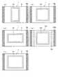
なお、本発明は、上記の実施の形態に限定されるものではなく、本発明の範囲内で種々の変更が可能である。例えば、上記実施の形態では、半導体装置1の半導体チップ3は、同じ大きさのものであったが、各半導体装置1の半導体チップ3は、必ずしも同じ大きさに限らず、例えば、図4(a)〜(e)に示すように、各種の大きさを有する半導体チップ3a・3b・3c・3dであってもよい。すなわち、このように各種の大きさの半導体チップ3a・3b・3c・3dを有していても、積層したときに、図5に示すように、第1裏面ランド部28a及び第1表面ランド部28bを外側部分に共通して形成し、共通信号として取り出すことができる。
【0054】
一方、本実施の形態では、図3(b)(c)に示すように、半導体装置20の第2裏面ランド部31は、第1裏面ランド部28a及び第1表面ランド部28bの内側において、これら第1裏面ランド部28a及び第1表面ランド部28bと平行にのみ形成されているが、特にこれに限定するものではない。例えば、図6(a)(b)(c)に示すように、最下段に配設される半導体装置20の第2裏面ランド部41として、第1裏面ランド部28a及び第1表面ランド部28bよりも内側であって、かつ絶縁基板42の略中央位置において略矩形に穿設された貫通孔部42aの周囲に形成することが可能である。この場合には、樹脂封止部24は、半導体装置20の中央部のみとし、その周囲4方向に半導体チップ23の外部端子である第2裏面ランド部41を配置する。
【0055】
一方、例えば、最下段の半導体装置20の出力と上段側の半導体装置1…の出力とを共通して用いることができる場合がある。この場合には、例えば、図7(a)(b)(c)に示すように、第1裏面ランド部28a及び第1表面ランド部28bの一部の領域51の端子について、上段側の半導体装置1…からの電気的導通が共通してとれるように接続する。これによって、領域51の第1裏面ランド部28a及び第1表面ランド部28bは、上段側の半導体装置1…のみの共通接続端子となる。
【0056】
一方、他の領域52の第1裏面ランド部28a及び第1表面ランド部28bについては、その半導体装置20の半導体チップ23からの出力も第1裏面ランド部28a及び第1表面ランド部28bに接続する。
【0057】
これによって、半導体装置20と半導体装置1とに共通して使用できる信号が有る場合には、他の領域52の第1裏面ランド部28a及び第1表面ランド部28bを共通信号端子として使用することができる。
【0058】
〔実施の形態2〕
本発明の他の実施の形態について図8及び図9に基づいて説明すれば、以下の通りである。なお、説明の便宜上、前記の実施の形態1の図面に示した部材と同一の機能を有する部材については、同一の符号を付し、その説明を省略する。
【0059】
本実施の形態の積層型半導体装置では、図8に示すように、最下段の半導体装置20が2個の半導体チップ23a・23bを縦に搭載したものからなっている。なお、本実施の形態では、半導体装置20は2個の半導体チップ23a・23bを搭載しているが、必ずしも2個に限らず、他の複数個であってもよい。
【0060】
また、上記の半導体チップ23a・23bは、縦方向に2個重ねて設けられているが、必ずしもこれに限らず、例えば、図9に示すように、水平方向に2個の半導体チップ23c・23dを並べることも可能である。なお、この場合には、同図に示すように、2個の半導体チップ23c・23dの間に、別途に外部接続端子を設けることが可能である。
【0061】
このように、本実施の形態の積層型半導体装置では、半導体装置20は2個の半導体チップ23a・23b又は半導体チップ23c・23dを搭載したものからなっている。
【0062】
この結果、例えばフラッシュメモリのメモリ容量を増やすために1個の半導体装置20に2個の半導体チップ23a・23b又は半導体チップ23c・23dを形成した場合においても、最大の大きさを有する半導体装置1…の領域の範囲内で多段に積層して電気的接続を可能とする積層型半導体装置を提供することができる。
【0063】
なお、本実施の形態の積層型半導体装置では、2個の半導体チップ23a・23bを搭載しているのは、最下段の半導体装置20であるが、本発明においては必ずしもこれに限らず、例えば、上段側の半導体装置1…のいずれかに複数個の半導体チップを搭載することも可能である。
【0064】
〔実施の形態3〕
本発明の他の実施の形態について図10に基づいて説明すれば、以下の通りである。なお、説明の便宜上、前記の実施の形態1及び実施の形態2の図面に示した部材と同一の機能を有する部材については、同一の符号を付し、その説明を省略する。
【0065】
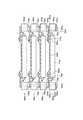
本実施の形態の積層型半導体装置は、図10に示すように、上段の3段が半導体装置1・1・1からなるとともに、下段の2段が半導体装置20・20からなっている。すなわち、本実施の形態では、前記実施の形態1及び実施の形態2に示した最下段の半導体装置20が2個以上の複数個有る場合について説明する。
【0066】
この場合には、全ての半導体装置1・1・1及び半導体装置20・20の端部に第1裏面ランド部28a及び第1表面ランド部28bを設ける。この第1裏面ランド部28a及び第1表面ランド部28bは、上側の半導体装置1…のための第1共通接続端子として機能するものとなっている。
【0067】
一方、下段の半導体装置20・20に対しては、上下間で共通して電気的導通を確保して外部出力するための第2共通接続端子である第2裏面ランド部31a及び第2表面ランド部31bを、上記第1裏面ランド部28a及び第1表面ランド部28bよりも内側の同心位置にそれぞれ設ける。この結果、機能の異なる半導体装置20・20が2個存在する場合であっても、第1裏面ランド部28a及び第1表面ランド部28bよりも内側に共通出力端子を形成することによって、機能の異なる半導体装置20・20間の導通がとれるものとなっている。
【0068】
なお、本実施の形態では、このように、半導体装置1・1・1が3段であり、半導体装置20・20が2段となっているが、必ずしもこれに限らず、いずれについても他の複数段であってもよい。
【0069】
このように、本実施の形態の積層型半導体装置では、2個の半導体装置20・20の半導体チップ23・23の半導体チップサイズが他の3個の半導体装置1…の半導体チップ3…の半導体チップサイズよりも小さい場合には、先ず、3個の半導体装置1…に対して上下間で共通して電気的導通を確保して外部出力するための第1共通接続端子としての裏面ランド部8a及び表面ランド部8b、並びに第1裏面ランド部28a及び第1表面ランド部28bが、全ての半導体装置1…・20・20の端部側の同心位置にそれぞれ配設される。
【0070】
また、最下段から連続して積層される半導体装置20・20に対して上下間で共通して電気的導通を確保して外部出力するための第2共通接続端子としての第2裏面ランド部31a及び第2表面ランド部31bは、最下段から連続して積層される半導体装置20・20における裏面ランド部8a及び表面ランド部8b、並びに第1裏面ランド部28a及び第1表面ランド部28bよりも内側の同心位置にそれぞれ設けられている。
【0071】
したがって、半導体チップサイズの小さい複数個の半導体装置20・20を最下段から連続して2段に積層し、かつ上述のように裏面ランド部8a及び表面ランド部8b、並びに第1裏面ランド部28a及び第1表面ランド部28bと第2裏面ランド部31a及び第2表面ランド部31bとを形成することによって、上段側の半導体装置1の実装面積を拡大することなく半導体チップサイズの小さい半導体装置20・20を積層することができる。
【0072】
この結果、サイズの異なる複数個の半導体装置1…・20・20であっても、最大の大きさを有する半導体装置1の領域の範囲内で多段に積層して電気的接続を可能とする積層型半導体装置を提供することができる。
【0073】
また、本実施の形態の積層型半導体装置では、上段側に設けられた半導体装置1…と、最下段から連続して積層される半導体装置20・20とは機能が異なるものである。
【0074】
したがって、例えば、上段側の半導体装置1…がメモリデバイス機能を有する一方、最下段から連続して積層される半導体装置20・20が液晶コントローラデバイス機能を有するという場合にも、上段側の半導体装置1の実装面積を拡大することなく半導体チップサイズの小さい2個の半導体装置20・20を積層することができる。
【0075】
また、本実施の形態の積層型半導体装置では、最下段から連続して積層される半導体装置20・20の半導体チップ23・23の半導体チップサイズは、上段側に設けられた半導体装置1…の半導体チップ3・3・3の半導体チップサイズよりも小さい。
【0076】
この結果、例えば、メモリデバイス機能を有する半導体装置1…と他の機能を有する半導体装置20・20とを積層する場合のように、サイズの異なる複数個の半導体装置であっても、最大の大きさを有する例えばメモリデバイス機能を有する半導体装置1の領域の範囲内で多段に積層して電気的接続を可能とする積層型半導体装置を提供することができる。
【0077】
なお、本実施の形態においても、複数個の半導体装置1…・20・20のうちのいずれかは、1個の半導体装置に複数個の半導体チップを搭載することが可能である。
【0078】
【発明の効果】
本発明の積層型半導体装置は、以上のように、複数個の半導体装置のうちの最下段の半導体装置を除く上段側の半導体装置に対して上下間で共通して電気的導通を確保して外部出力するための第1共通接続端子が、全ての半導体装置の端部側の一部の領域における同心位置にそれぞれ配設されるとともに、上記複数個の半導体装置のうちの最下段の半導体装置から外部出力するための一部の外部出力端子である第2接続端子は、上記最下段の半導体装置の第1共通接続端子よりも内側に配設されているとともに、上記最下段の半導体装置における上記第2接続端子とは異なる他の外部出力端子は、上記最下段を除く上段側の半導体装置と共通に外部出力するための接続端子として、上記端部側における第1共通接続端子が配設された領域以外の他の領域に配設されているものである。
【0079】
それゆえ、1個の半導体装置の半導体チップサイズが他の半導体装置の半導体チップサイズよりも小さい場合であっても、半導体チップサイズの小さい半導体装置を最下段にして積層しかつ上述のように第1共通接続端子及び第2接続端子を形成することによって、上段側の半導体装置の実装面積を拡大することなく半導体チップサイズの小さい半導体装置を積層することができる。
【0080】
したがって、サイズの異なる半導体装置であっても、最大の大きさを有する半導体装置領域の範囲内で多段に積層して電気的接続を可能とする積層型半導体装置を提供することができるという効果を奏する。
【図面の簡単な説明】
【図1】 本発明における積層型半導体装置の実施の一形態を示す断面図である。
【図2】 (a)は上記積層型半導体装置における1個の半導体装置の構成を示す平面図、(b)は積層型半導体装置における1個の半導体装置の構成を示す断面図、(c)は積層型半導体装置における1個の半導体装置の構成を示す底面図である。
【図3】 (a)は最下段の半導体装置の構成を示す平面図、(b)は最下段の半導体装置の構成を示す断面図、(c)は最下段の半導体装置の構成を示す底面図である。
【図4】 (a)〜(e)は半導体チップの大きさがそれぞれ異なる場合の各半導体装置の構成を示す平面図である。
【図5】 上記各半導体装置を積層した状態を示す断面図である。
【図6】 (a)最下段の半導体装置の変形例を示す平面図、(b)は最下段の半導体装置の変形例を示す断面図、(c)は最下段の半導体装置の変形例を示す底面図である。
【図7】 (a)最下段の半導体装置の他の変形例を示す平面図、(b)は最下段の半導体装置の他の変形例を示す断面図、(c)は最下段の半導体装置の他の変形例を示す底面図である。
【図8】 本発明における積層型半導体装置の他の実施の形態を示す断面図である。
【図9】 上記積層型半導体装置の変形例を示す断面図である。
【図10】 本発明における積層型半導体装置のさらに他の実施の形態を示す断面図である。
【図11】 従来の積層型半導体装置を示す断面図である。
【符号の説明】
1 半導体装置
2 絶縁基板
3 半導体チップ
8a 裏面ランド部(第1共通接続端子)
8b 表面ランド部(第1共通接続端子)
10 半田ボール
20 半導体装置
22 絶縁基板
23 半導体チップ
23a 半導体チップ
23b 半導体チップ
23c 半導体チップ
23d 半導体チップ
28a 第1裏面ランド部(第1共通接続端子)
28b 第1表面ランド部(第1共通接続端子)
30 半田ボール
31 第2裏面ランド部(第2接続端子)
31a 第2裏面ランド部(第2共通接続端子)
31b 第2表面ランド部(第2共通接続端子)[0001]
BACKGROUND OF THE INVENTION
The present invention relates to a stacked semiconductor device for stacking a plurality of semiconductor devices each having a semiconductor chip, thereby achieving high functionality, downsizing, and thinning.
[0002]
[Prior art]
In recent years, QFP (Quad Flat Package) type and BGA (Ball Grid) have been adopted to meet the demands for miniaturization of electronic equipment and to be suitable for automation of assembly processes.
Allay type CSP (Chip Size Package) type semiconductor devices are widely used.
[0003]
In these semiconductor devices, a multi-chip semiconductor device in which a plurality of film carrier semiconductor modules as semiconductor devices are stacked and electrically connected to increase the mounting efficiency is disclosed in, for example, Japanese Patent Laid-Open No. 10-163414. .
[0004]
As shown in FIG. 11, the multi-chip semiconductor device has film
[0005]
In the film carrier semiconductor module 88a,
[0006]
The
[0007]
In the above description, the configuration of the lowermost film carrier semiconductor module 88a shown in FIG. 11 has been described, but from the bottom, the second, third, and fourth stage film
[0008]
Here, the structure for electrically connecting the above-mentioned adjacent film
[0009]
First, a solder ball is provided on the
[0010]
[Problems to be solved by the invention]
By the way, in the conventional stacked semiconductor device, when electrical conduction is made between the upper and lower sides, the same signal terminal ensures electrical conduction between the upper and lower sides at the same terminal position. That is, in this type of stacked semiconductor device, the connection terminals between the upper and lower packages must be arranged outside the semiconductor chip.
[0011]
Here, in a semiconductor device having a large semiconductor chip size such as a memory device, the package outer size, that is, the package mounting area, tends to be larger than the package size other than the semiconductor device such as a memory device.
[0012]
Therefore, in the conventional stacked semiconductor device, the following problems arise when a semiconductor device having a function different from that of the memory device is stacked together with the semiconductor devices of the plurality of memory devices.
[0013]
That is, the semiconductor device having a function different from that of the memory device is different in size from the semiconductor device of the memory device, and as described above, the semiconductor device is concentrically aligned and electrically connected in the outer portion of the semiconductor device. I can't. As a result, a semiconductor device having a function different from that of the memory device must be mounted in a different part, so that the mounting substrate becomes large and the requirement for a device such as a portable device that requires downsizing cannot be satisfied. Has the problem.
[0014]
The present invention has been made in view of the above-described conventional problems, and the object thereof is to stack multiple layers within the range of the semiconductor device region having the maximum size even if the semiconductor devices have different sizes. It is an object of the present invention to provide a stacked semiconductor device that enables electrical connection.
[0015]
[Means for Solving the Problems]
In order to solve the above-described problem, a stacked semiconductor device according to the present invention is a stacked semiconductor device in which a plurality of semiconductor devices are stacked, and an upper side of the plurality of semiconductor devices excluding a lowermost semiconductor device. A first common connection terminal for ensuring electrical continuity between the upper and lower sides of the semiconductor device and outputting to the outside is provided on the end side of all the semiconductor devices.In some areasEach of the plurality of semiconductor devices is disposed at a concentric position, and is the lowermost semiconductor device among the plurality of semiconductor devices.The second connection terminal which is a part of the external output terminal for external output fromThe lowermost semiconductor device is disposed on the inner side than the first common connection terminal of the lowermost semiconductor device.Other external output terminals different from the second connection terminal areAs a connection terminal for external output in common with the semiconductor device on the upper stage excluding the lowermost stage,It is disposed in a region other than the region where the first common connection terminal is disposed on the end side.It is a feature. Note that the vertical relationship of the semiconductor device does not matter whether the front side or the back side is vertical. In other words, the vertical relationship of the semiconductor devices is relative, and a semiconductor device of a different type from the other semiconductor devices can be stacked on the uppermost stage.
[0016]
First, for example, since a semiconductor device such as a memory device has a large area of a semiconductor chip, a terminal for external connection is arranged outside the semiconductor chip. Therefore, when a plurality of semiconductor devices such as the same memory device are stacked, as the common signal line, the external connection terminals can be easily connected by concentrically connecting the external connection terminals. A common output signal can be taken out from.
[0017]
However, when a semiconductor device such as a plurality of memory devices and a semiconductor device having a function different from these are stacked together, generally, the semiconductor chip of the semiconductor device having a function different from that of the memory device has a size. Because they are small, they cannot be stacked together. That is, it is difficult to extract a common output signal.
[0018]
Therefore, in the present invention, first of all, the upper semiconductor device excluding the lowermost semiconductor device of the plurality of semiconductor devices is electrically connected to the upper and lower sides to ensure electrical continuity and externally output. One common connection terminal is disposed at a concentric position on the end side of all the semiconductor devices. Therefore, the lowermost semiconductor device is also provided with the first common connection terminal for transmitting the electrical signals of the upper semiconductor devices to the mounting substrate. That is, in the present invention, the first common connection terminal provided in the lowermost semiconductor device functions as a stacking terminal for outputting the output from the upper semiconductor device to the outside.
[0019]
On the other hand, the second connection terminal for external output in the lowermost semiconductor device is disposed inside the first common connection terminal of the lowermost semiconductor device. Therefore, in the lowermost semiconductor device, it is possible to output to the outside from the second connection terminal disposed on the inner side.
[0020]
As a result, even when the semiconductor chip size of one semiconductor device is smaller than the semiconductor chip size of the other semiconductor device, the semiconductor devices having the small semiconductor chip size are stacked at the bottom and the first semiconductor device is stacked as described above. By forming the one common connection terminal and the second connection terminal, it is possible to stack semiconductor devices having a small semiconductor chip size without increasing the mounting area of the upper semiconductor device.
[0021]
Therefore, even if the semiconductor devices have different sizes, a stacked semiconductor device that can be electrically connected by stacking in multiple stages within the range of the semiconductor device region having the maximum size can be provided.
[0022]
In the stacked semiconductor device of the present invention, in the stacked semiconductor device described above, there is a function between the semiconductor device provided on the upper stage side and the semiconductor device stacked on the lowermost stage or continuously from the lowermost stage. It is characterized by being different.
[0023]
According to the above invention, the function of the semiconductor device provided on the upper side is different from that of the lowermost semiconductor device or the semiconductor device continuously stacked from the lowermost level. Even when the lowermost semiconductor device has a liquid crystal controller device function while having a device function, a plurality of semiconductor devices having a small semiconductor chip size are stacked without increasing the mounting area of the upper semiconductor device. Can do.
[0024]
In addition, the stacked semiconductor device of the present invention is characterized in that, in the above-described stacked semiconductor device, a semiconductor device including a semiconductor chip larger than a chip size provided in the lowermost semiconductor device is included on the upper stage side.
[0025]
As a result, for example, a memory having a maximum size, for example, a plurality of semiconductor devices having different sizes as in the case where a semiconductor device having a memory device function and a semiconductor device having another function are stacked. It is possible to provide a stacked semiconductor device that can be stacked in multiple stages within the range of a semiconductor device region having a device function to enable electrical connection.
[0026]
According to another aspect of the present invention, there is provided a stacked semiconductor device, wherein any one of the plurality of semiconductor devices includes a plurality of semiconductor chips mounted on one semiconductor device. It is characterized by that.
[0027]
According to the above invention, since any one of the plurality of semiconductor devices is formed by mounting a plurality of semiconductor chips on one semiconductor device, for example, to increase the memory capacity of the flash memory. Provided is a stacked semiconductor device in which even when two semiconductor chips are formed in one semiconductor device, the semiconductor devices can be electrically connected by being stacked in multiple stages within the range of the semiconductor device region having the maximum size. be able to.
[0028]
DETAILED DESCRIPTION OF THE INVENTION
[Embodiment 1]
One embodiment of the present invention will be described with reference to FIGS. 1 to 7 as follows.
[0029]
In the stacked semiconductor device according to the present embodiment, as shown in FIG. 1,
[0030]
Here, the upper four-
[0031]
On the other hand, the
[0032]
Here, as described above, the
[0033]
The configurations of the upper four
[0034]
In the
[0035]
An
[0036]
A through-hole portion 9 penetrating the insulating
[0037]
For example,
[0038]
On the other hand, the
[0039]
Here, in the present embodiment, the first back
[0040]
That is, the first back
[0041]
As a result, the electrical continuity for external output commonly secured in the plurality of stacked
[0042]
On the other hand, in the present embodiment, a second back
[0043]
In the stacked semiconductor device according to the present embodiment, the
[0044]
In the stacked semiconductor device thus formed, it is possible to mount the
[0045]
Thus, in the stacked semiconductor device according to the present embodiment, the
[0046]
Therefore, the
[0047]
On the other hand, the second back
[0048]
As a result, even when the semiconductor chip size of the
[0049]
Therefore, even if the semiconductor devices have different sizes, it is possible to provide a stacked semiconductor device that can be electrically connected by stacking in multiple stages within the region of the
[0050]
Further, in the stacked semiconductor device of the present embodiment, the functions of the
[0051]
In the stacked semiconductor device of the present embodiment, the semiconductor chip size of the
[0052]
As a result, even when a plurality of semiconductor devices having different sizes are stacked, as in the case of stacking the
[0053]
In addition, this invention is not limited to said embodiment, A various change is possible within the scope of the present invention. For example, in the above embodiment, the
[0054]
On the other hand, in the present embodiment, as shown in FIGS. 3B and 3C, the second back
[0055]
On the other hand, for example, the output of the
[0056]
On the other hand, for the first back
[0057]
Thus, when there is a signal that can be used in common between the
[0058]
[Embodiment 2]
The following will describe another embodiment of the present invention with reference to FIGS. For convenience of explanation, members having the same functions as those shown in the drawings of the first embodiment are given the same reference numerals, and descriptions thereof are omitted.
[0059]
In the stacked semiconductor device according to the present embodiment, as shown in FIG. 8, the
[0060]
Further, the two
[0061]
As described above, in the stacked semiconductor device of the present embodiment, the
[0062]
As a result, for example, even when two
[0063]
In the stacked semiconductor device of the present embodiment, it is the
[0064]
[Embodiment 3]
The following will describe another embodiment of the present invention with reference to FIG. For convenience of explanation, members having the same functions as those shown in the drawings of
[0065]
In the stacked semiconductor device according to the present embodiment, as shown in FIG. 10, the upper three stages are composed of
[0066]
In this case, the first back
[0067]
On the other hand, for the
[0068]
In the present embodiment, the
[0069]
As described above, in the stacked semiconductor device according to the present embodiment, the semiconductor chip size of the semiconductor chips 23 of the two
[0070]
Further, the second back
[0071]
Therefore, a plurality of
[0072]
As a result, even for a plurality of
[0073]
In the stacked semiconductor device of the present embodiment, the functions of the
[0074]
Therefore, for example, even when the
[0075]
Further, in the stacked semiconductor device of the present embodiment, the semiconductor chip size of the semiconductor chips 23 and 23 of the
[0076]
As a result, for example, even when a plurality of semiconductor devices having different sizes are stacked, as in the case where the
[0077]
Also in this embodiment, any one of the plurality of
[0078]
【The invention's effect】
As described above, the stacked semiconductor device of the present invention secures electrical continuity in common between the upper and lower semiconductor devices excluding the lowermost semiconductor device among the plurality of semiconductor devices. A first common connection terminal for external output is provided on the end side of all semiconductor devices.In some areasEach of the plurality of semiconductor devices is disposed at a concentric position, and is the lowermost semiconductor device among the plurality of semiconductor devices.Some external output terminals for external output fromThe second connection terminal is disposed inside the first common connection terminal of the lowermost semiconductor device, and in the lowermost semiconductor device.Other external output terminals different from the second connection terminal areAs a connection terminal for external output in common with the semiconductor device on the upper stage excluding the lowermost stage,It is disposed in a region other than the region where the first common connection terminal is disposed on the end side.
[0079]
Therefore, even when the semiconductor chip size of one semiconductor device is smaller than the semiconductor chip size of the other semiconductor device, the semiconductor devices having the small semiconductor chip size are stacked at the lowest level and the first as described above. By forming the one common connection terminal and the second connection terminal, it is possible to stack semiconductor devices having a small semiconductor chip size without increasing the mounting area of the upper semiconductor device.
[0080]
Therefore, even if the semiconductor devices have different sizes, it is possible to provide a stacked semiconductor device that can be stacked in multiple stages within the range of the semiconductor device region having the maximum size and can be electrically connected. Play.
[Brief description of the drawings]
FIG. 1 is a cross-sectional view showing an embodiment of a stacked semiconductor device according to the present invention.
2A is a plan view showing the configuration of one semiconductor device in the stacked semiconductor device, FIG. 2B is a cross-sectional view showing the configuration of one semiconductor device in the stacked semiconductor device, and FIG. FIG. 3 is a bottom view showing the configuration of one semiconductor device in a stacked semiconductor device.
3A is a plan view showing the configuration of the lowermost semiconductor device, FIG. 3B is a cross-sectional view showing the configuration of the lowermost semiconductor device, and FIG. 3C is a bottom view showing the configuration of the lowermost semiconductor device. FIG.
FIGS. 4A to 4E are plan views showing the configuration of each semiconductor device when the sizes of the semiconductor chips are different from each other. FIGS.
FIG. 5 is a cross-sectional view showing a state where the semiconductor devices are stacked.
6A is a plan view showing a modified example of the lowermost semiconductor device, FIG. 6B is a cross-sectional view showing a modified example of the lowermost semiconductor device, and FIG. 6C is a modified example of the lowermost semiconductor device; It is a bottom view shown.
7A is a plan view illustrating another modification of the lowermost semiconductor device, FIG. 7B is a cross-sectional view illustrating another modification of the lowermost semiconductor device, and FIG. 7C is a lowermost semiconductor device. It is a bottom view which shows the other modification.
FIG. 8 is a cross-sectional view showing another embodiment of a stacked semiconductor device according to the present invention.
FIG. 9 is a cross-sectional view showing a modified example of the stacked semiconductor device.
FIG. 10 is a cross-sectional view showing still another embodiment of a stacked semiconductor device according to the present invention.
FIG. 11 is a cross-sectional view showing a conventional stacked semiconductor device.
[Explanation of symbols]
1 Semiconductor device
2 Insulating substrate
3 Semiconductor chip
8a Back land part (first common connection terminal)
8b Surface land (first common connection terminal)
10 Solder balls
20 Semiconductor device
22 Insulating substrate
23 Semiconductor chip
23a Semiconductor chip
23b Semiconductor chip
23c Semiconductor chip
23d semiconductor chip
28a First back surface land (first common connection terminal)
28b First surface land portion (first common connection terminal)
30 Solder balls
31 Second back surface land (second connection terminal)
31a Second back surface land (second common connection terminal)
31b Second surface land portion (second common connection terminal)
Claims (4)
Translated fromJapanese上記複数個の半導体装置のうちの最下段の半導体装置を除く上段側の半導体装置に対して上下間で共通して電気的導通を確保して外部出力するための第1共通接続端子が、全ての半導体装置の端部側の一部の領域における同心位置にそれぞれ配設されるとともに、
上記複数個の半導体装置のうちの最下段の半導体装置から外部出力するための一部の外部出力端子である第2接続端子は、上記最下段の半導体装置の第1共通接続端子よりも内側に配設されているとともに、
上記最下段の半導体装置における上記第2接続端子とは異なる他の外部出力端子は、上記最下段を除く上段側の半導体装置と共通に外部出力するための接続端子として、上記端部側における第1共通接続端子が配設された領域以外の他の領域に配設されていることを特徴とする積層型半導体装置。In a stacked semiconductor device in which a plurality of semiconductor devices are stacked,
The first common connection terminal for ensuring electrical continuity between the upper and lower semiconductor devices excluding the lowermost semiconductor device among the plurality of semiconductor devices and for external output is all provided. Are disposed at concentric positionsin apartial region on the end side of the semiconductor device,
Of the plurality of semiconductor devices, a second connection terminal, which is a part of an external output terminal for external output from the lowermost semiconductor device, is located inside the first common connection terminal of the lowermost semiconductor device. Being arranged,
Another external output terminal different from the second connection terminal in the lowermost semiconductor device is a connection terminal for external output in common with the upper semiconductor device excluding the lowermost stage, and is connected to the second output terminal on theend side. 1. A stacked semiconductor device, wherein the stacked semiconductor deviceis disposed in a region other than a region where one common connection terminal is disposed .
Priority Applications (1)
| Application Number | Priority Date | Filing Date | Title |
|---|---|---|---|
| JP2001331181AJP3850712B2 (en) | 2001-10-29 | 2001-10-29 | Multilayer semiconductor device |
Applications Claiming Priority (1)
| Application Number | Priority Date | Filing Date | Title |
|---|---|---|---|
| JP2001331181AJP3850712B2 (en) | 2001-10-29 | 2001-10-29 | Multilayer semiconductor device |
Publications (2)
| Publication Number | Publication Date |
|---|---|
| JP2003133516A JP2003133516A (en) | 2003-05-09 |
| JP3850712B2true JP3850712B2 (en) | 2006-11-29 |
Family
ID=19146799
Family Applications (1)
| Application Number | Title | Priority Date | Filing Date |
|---|---|---|---|
| JP2001331181AExpired - Fee RelatedJP3850712B2 (en) | 2001-10-29 | 2001-10-29 | Multilayer semiconductor device |
Country Status (1)
| Country | Link |
|---|---|
| JP (1) | JP3850712B2 (en) |
Families Citing this family (3)
| Publication number | Priority date | Publication date | Assignee | Title |
|---|---|---|---|---|
| JP2006032379A (en)* | 2004-07-12 | 2006-02-02 | Akita Denshi Systems:Kk | Laminate semiconductor device and its manufacturing method |
| JP4199724B2 (en) | 2004-12-03 | 2008-12-17 | エルピーダメモリ株式会社 | Stacked semiconductor package |
| JP2007250764A (en)* | 2006-03-15 | 2007-09-27 | Elpida Memory Inc | Semiconductor device and manufacturing method therefor |
- 2001
- 2001-10-29JPJP2001331181Apatent/JP3850712B2/ennot_activeExpired - Fee Related
Also Published As
| Publication number | Publication date |
|---|---|
| JP2003133516A (en) | 2003-05-09 |
Similar Documents
| Publication | Publication Date | Title |
|---|---|---|
| US7495327B2 (en) | Chip stacking structure | |
| US6876074B2 (en) | Stack package using flexible double wiring substrate | |
| US6731009B1 (en) | Multi-die assembly | |
| JP3512657B2 (en) | Semiconductor device | |
| US7411281B2 (en) | Integrated circuit device package having both wire bond and flip-chip interconnections and method of making the same | |
| US6369448B1 (en) | Vertically integrated flip chip semiconductor package | |
| KR100430861B1 (en) | Wiring substrate, semiconductor device and package stack semiconductor device | |
| US7755188B2 (en) | Method and apparatus for stacking electrical components using via to provide interconnection | |
| JP2005045251A (en) | Stacked semiconductor chip BGA package and manufacturing method thereof | |
| JP2004172157A (en) | Semiconductor package and package stack semiconductor device | |
| US7615858B2 (en) | Stacked-type semiconductor device package | |
| KR20020061812A (en) | Ball grid array type multi chip package and stack package | |
| JP2001156251A (en) | Semiconductor device | |
| JPH0730059A (en) | Multichip module | |
| JP2000228468A (en) | Semiconductor chip and semiconductor device | |
| JP3850712B2 (en) | Multilayer semiconductor device | |
| US7265441B2 (en) | Stackable single package and stacked multi-chip assembly | |
| KR20010063236A (en) | Stack package and manufacturing method thereof | |
| CN1964036A (en) | Stacked Die Package Structure | |
| KR101141707B1 (en) | Semiconductor package and method of manufacturing the same | |
| KR100674411B1 (en) | Semiconductor Package Using Core Ball and Manufacturing Method Thereof | |
| KR100437821B1 (en) | semiconductor package and metod for fabricating the same | |
| JP2001118954A (en) | Semiconductor device | |
| KR20040059741A (en) | Packaging method of multi chip module for semiconductor | |
| JP3418759B2 (en) | Semiconductor package |
Legal Events
| Date | Code | Title | Description |
|---|---|---|---|
| A621 | Written request for application examination | Free format text:JAPANESE INTERMEDIATE CODE: A621 Effective date:20040618 | |
| A977 | Report on retrieval | Free format text:JAPANESE INTERMEDIATE CODE: A971007 Effective date:20051216 | |
| A131 | Notification of reasons for refusal | Free format text:JAPANESE INTERMEDIATE CODE: A131 Effective date:20060110 | |
| A521 | Request for written amendment filed | Free format text:JAPANESE INTERMEDIATE CODE: A523 Effective date:20060310 | |
| RD02 | Notification of acceptance of power of attorney | Free format text:JAPANESE INTERMEDIATE CODE: A7422 Effective date:20060310 | |
| A131 | Notification of reasons for refusal | Free format text:JAPANESE INTERMEDIATE CODE: A131 Effective date:20060425 | |
| A521 | Request for written amendment filed | Free format text:JAPANESE INTERMEDIATE CODE: A523 Effective date:20060623 | |
| TRDD | Decision of grant or rejection written | ||
| A01 | Written decision to grant a patent or to grant a registration (utility model) | Free format text:JAPANESE INTERMEDIATE CODE: A01 Effective date:20060829 | |
| A61 | First payment of annual fees (during grant procedure) | Free format text:JAPANESE INTERMEDIATE CODE: A61 Effective date:20060830 | |
| R150 | Certificate of patent or registration of utility model | Free format text:JAPANESE INTERMEDIATE CODE: R150 | |
| FPAY | Renewal fee payment (event date is renewal date of database) | Free format text:PAYMENT UNTIL: 20090908 Year of fee payment:3 | |
| FPAY | Renewal fee payment (event date is renewal date of database) | Free format text:PAYMENT UNTIL: 20100908 Year of fee payment:4 | |
| FPAY | Renewal fee payment (event date is renewal date of database) | Free format text:PAYMENT UNTIL: 20110908 Year of fee payment:5 | |
| FPAY | Renewal fee payment (event date is renewal date of database) | Free format text:PAYMENT UNTIL: 20120908 Year of fee payment:6 | |
| FPAY | Renewal fee payment (event date is renewal date of database) | Free format text:PAYMENT UNTIL: 20130908 Year of fee payment:7 | |
| LAPS | Cancellation because of no payment of annual fees |