JP3846970B2 - Ionization sputtering equipment - Google Patents
Ionization sputtering equipmentDownload PDFInfo
- Publication number
- JP3846970B2 JP3846970B2JP11190297AJP11190297AJP3846970B2JP 3846970 B2JP3846970 B2JP 3846970B2JP 11190297 AJP11190297 AJP 11190297AJP 11190297 AJP11190297 AJP 11190297AJP 3846970 B2JP3846970 B2JP 3846970B2
- Authority
- JP
- Japan
- Prior art keywords
- frequency coil
- ionization
- substrate
- shield
- coil
- Prior art date
- Legal status (The legal status is an assumption and is not a legal conclusion. Google has not performed a legal analysis and makes no representation as to the accuracy of the status listed.)
- Expired - Fee Related
Links
Images


Classifications
- H—ELECTRICITY
- H01—ELECTRIC ELEMENTS
- H01J—ELECTRIC DISCHARGE TUBES OR DISCHARGE LAMPS
- H01J37/00—Discharge tubes with provision for introducing objects or material to be exposed to the discharge, e.g. for the purpose of examination or processing thereof
- H01J37/32—Gas-filled discharge tubes
- H01J37/32009—Arrangements for generation of plasma specially adapted for examination or treatment of objects, e.g. plasma sources
- H01J37/32082—Radio frequency generated discharge
- H01J37/321—Radio frequency generated discharge the radio frequency energy being inductively coupled to the plasma
- C—CHEMISTRY; METALLURGY
- C23—COATING METALLIC MATERIAL; COATING MATERIAL WITH METALLIC MATERIAL; CHEMICAL SURFACE TREATMENT; DIFFUSION TREATMENT OF METALLIC MATERIAL; COATING BY VACUUM EVAPORATION, BY SPUTTERING, BY ION IMPLANTATION OR BY CHEMICAL VAPOUR DEPOSITION, IN GENERAL; INHIBITING CORROSION OF METALLIC MATERIAL OR INCRUSTATION IN GENERAL
- C23C—COATING METALLIC MATERIAL; COATING MATERIAL WITH METALLIC MATERIAL; SURFACE TREATMENT OF METALLIC MATERIAL BY DIFFUSION INTO THE SURFACE, BY CHEMICAL CONVERSION OR SUBSTITUTION; COATING BY VACUUM EVAPORATION, BY SPUTTERING, BY ION IMPLANTATION OR BY CHEMICAL VAPOUR DEPOSITION, IN GENERAL
- C23C14/00—Coating by vacuum evaporation, by sputtering or by ion implantation of the coating forming material
- C23C14/22—Coating by vacuum evaporation, by sputtering or by ion implantation of the coating forming material characterised by the process of coating
- C23C14/34—Sputtering
- H—ELECTRICITY
- H01—ELECTRIC ELEMENTS
- H01J—ELECTRIC DISCHARGE TUBES OR DISCHARGE LAMPS
- H01J37/00—Discharge tubes with provision for introducing objects or material to be exposed to the discharge, e.g. for the purpose of examination or processing thereof
- H01J37/32—Gas-filled discharge tubes
- H01J37/34—Gas-filled discharge tubes operating with cathodic sputtering
- H01J37/3402—Gas-filled discharge tubes operating with cathodic sputtering using supplementary magnetic fields
- H01J37/3405—Magnetron sputtering
- H01J37/3408—Planar magnetron sputtering
Landscapes
- Chemical & Material Sciences (AREA)
- Engineering & Computer Science (AREA)
- Physics & Mathematics (AREA)
- Plasma & Fusion (AREA)
- Analytical Chemistry (AREA)
- Materials Engineering (AREA)
- Chemical Kinetics & Catalysis (AREA)
- Mechanical Engineering (AREA)
- Metallurgy (AREA)
- Organic Chemistry (AREA)
- Physical Vapour Deposition (AREA)
- Electrodes Of Semiconductors (AREA)
- Physical Deposition Of Substances That Are Components Of Semiconductor Devices (AREA)
Description
Translated fromJapanese【0001】
【発明の属する技術分野】
本願の発明は、各種半導体デバイスの製作に使用されるスパッタリング装置に関し、特に、スパッタ粒子をイオン化する機能を備えたイオン化スパッタリング装置に関するものである。
【0002】
【従来の技術】
各種メモリやロジック等の半導体デバイスでは、各種配線膜の形成や異種層の相互拡散を防止するバリア膜の作成等の際にスパッタリングプロセスを用いており、スパッタリング装置が多用されている。このようなスパッタリング装置に要求される特性は色々あるが、基板に形成されたホールの内面にカバレッジ性よく被覆できることが、最近強く求められている。
【0003】
具体的に説明すると、例えばバリア膜の場合、ホールの周囲の面に対するホールの底面への成膜速度の比であるボトムカバレッジ率の向上が最近特に強く要請されている。というのは、集積度の増加を背景として、コンタクトホール等のホールはそのアスペクト比(ホールの開口の大きさに対するホールの深さの比)が年々高くなってきており、このような高アスペクト比のホールに対しては、従来のスパッタリングの手法では、ボトムカバレッジ率よく成膜が行えないことが多いからである。ボトムカバレッジ率が低下すると、ホールの底面でバリア膜が薄くなり、ジャンクションリーク等のデバイス特性に致命的な欠陥を与える恐れがある。
【0004】
ボトムカバレッジ率を向上させるスパッタリングの手法として、コリメートスパッタや低圧遠隔スパッタ等の手法がこれまで開発されてきた。これらの手法の詳細な説明は省略するが、いずれも中性スパッタ粒子を多く基板に垂直に入射させようとする試みである。
【0005】
しかしながら、コリメートスパッタではコリメーターの部分にスパッタ粒子が堆積して損失になるために成膜速度が低下する問題があり、また、低圧遠隔スパッタでは、圧力を低くしターゲットと基板との距離を長くするため本質的に成膜速度が低下する問題がある。このような問題のため、コリメートスパッタでは64メガビットまで、低圧遠隔スパッタでは256メガビットの第一世代程度までが限界であると予測されており、256メガビット以上の次世代のデバイス製作に利用可能な実用的な手法の模索が行われている。
【0006】
このような要求に応えるものとして、イオン化スパッタの手法が有力ではないかと最近考えられている。イオン化スパッタは、ターゲットから放出されるスパッタ粒子をイオン化し、イオンの作用によってホール内に効率よくスパッタ粒子を到達させる手法である。イオン化スパッタによると、コリメートスパッタや低圧遠隔スパッタに比べて遥かに高いボトムカバレッジ率が得られることが確認されている。
【0007】
イオン化スパッタの典型的な構成としては、基板とターゲットの間のスパッタ粒子の飛行経路上にプラズマを形成し、スパッタ粒子がプラズマを通過する際にイオン化するようにする。プラズマとしては、誘導結合型プラズマが通常形成される。具体的には、飛行経路上のイオン化を行う空間(以下、イオン化空間)を取り囲むようにして高周波コイルを設け、この高周波コイルに所定の高周波を供給して高周波コイルの内部にプラズマを形成するようにする。プラズマ中には高周波電流が流れ、プラズマと高周波コイルは誘導性結合する。このため、誘導結合型プラズマと呼ばれる。
【0008】
【発明が解決しようとする課題】
しかしながら、発明者の検討によると、上記イオン化スパッタの構成では、以下のような課題を抱えていることが判明した。
まず第一に、充分な強度の高周波電界をイオン化空間に設定するため、高周波コイルは通常スパッタチャンバーの内部に配設されるが、プラズマによって高周波コイルがスパッタされ、スパッタされた高周波コイルの材料が基板に達する結果、基板を汚損する問題がある。
第二に、スパッタチャンバー内をガスは拡散していくため、高周波コイルの外側でもプラズマが形成される場合があり、このような場所に形成されるプラズマはイオン化に不要なものであるのみならず、その場所に配置されている部材に損傷を与える場合がある。
第三に、プラズマを形成する場合、スパッタ放電のためのガスを導入するガス導入手段を兼用するが、スパッタ放電のために最適なガス導入とイオン化用のプラズマ形成のために最適なガス導入の構成とは異なる。このため、プラズマ形成のために効率よくガスが供給できず、プラズマ形成効率が悪い。
本願の発明は、このような課題を解決するためになされたものであり、イオン化スパッタが抱えるこのような問題を解決し、次世代のデバイスの製作に有効な実用的なイオン化スパッタリング装置を提供することを目的としている。
【0009】
【課題を解決するための手段】
上記課題を解決するため、本願の請求項1記載の発明は、排気系を備えたスパッタチャンバーと、スパッタチャンバー内に設けられたターゲットと、ターゲットをスパッタするスパッタ電極と、スパッタチャンバー内に所定のガスを導入するガス導入手段と、スパッタによってターゲットから放出されたスパッタ粒子をイオン化させるイオン化手段と、イオン化したスパッタ粒子が入射する位置に基板を保持する基板ホルダーとを備えたイオン化スパッタリング装置であって、
前記イオン化手段は、ターゲットと基板ホルダーとの間のイオン化空間を取り囲むようにスパッタチャンバー内に設けられた高周波コイルと、この高周波コイルに所定の高周波を供給してイオン化空間に高周波誘導結合型プラズマを形成する高周波電源とから構成されており、
当該高周波コイルの外側には、高周波コイルの内側にプラズマを閉じ込めるシールドが設けられており、
このシールドは、金属製の部材で形成され電気的に接地されているとともに、このシールドは、高周波コイルが延びる方向に同様に延びるものであって、断面で見ると、高周波コイルの各部をそれぞれ外側から取り囲んで覆うとともに、内側にイオン化空間に向けて高周波が放射されるよう高周波通過用開口を設けた形状であり、
高周波通過用開口は、高周波コイルの全長にわたって形成されたスリットであるという構成を有する。
また、上記課題を解決するため、請求項2記載の発明は、上記請求項1の構成において、前記シールドは、高周波コイルを臨む表面が、高周波コイルから放射される電界の等電位面に沿った形状になるように形成されているという構成を有する。
また、上記課題を解決するため、請求項3記載の発明は、上記請求項1又は2の構成において、前記シールドは、高周波コイルから高周波通過用開口を通しては基板上のいずれの点も見通せない形状であるという構成を有する。
また、上記課題を解決するため、請求項4記載の発明は、上記請求項1又は2の構成において、前記シールドは、高周波コイルから高周波通過用開口を通しては基板上及びターゲットの被スパッタ面上のいずれの点も見通せない形状であるという構成を有する。
また、上記課題を解決するため、請求項5記載の発明は、上記請求項1乃至4いずれかの構成において、前記シールドの内面には、当該内面への堆積膜が落下しないようにする凹凸が設けられているという構成を有する。
また、上記課題を解決するため、請求項6記載の発明は、上記請求項1乃至5いずれかの構成において、前記高周波コイルは、基板に作成する薄膜の材料であるターゲットの材料と同一の材料で形成されているという構成を有する。
また、上記課題を解決するため、請求項7記載の発明は、上記請求項1乃至6いずれかの構成において、前記イオン化したスパッタ粒子を基板に引き込むために基板に垂直な方向に電界を設定する電界設定手段とを備えているという構成を有する。
また、上記課題を解決するため、請求項8記載の発明は、上記請求項1乃至7いずれかの構成において、前記高周波コイルは、内部が中空であって前記イオン化空間を臨む内側面にガス吹き出し穴が均等に形成されており、前記ガス導入手段の補助チャンバー内配管が接続されてガス吹き出し穴から所定のガスをイオン化空間に導入することができるようになっているという構成を有する。
また、上記課題を解決するため、請求項9記載の発明は、上記請求項8の構成において、前記ガス導入手段は、前記高周波コイルに供給するガスの温度を所定温度に維持する温度調節器を有し、高周波コイルの温度調節をすることが可能となっているという構成を有する。
【0010】
【発明の実施の形態】
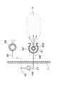
以下、本願発明の実施の形態について説明する。まず、第一の実施形態について説明する。図1は、本願発明の第一の実施形態のスパッタリング装置の構成を説明する正面概略図である。
図1に示すように、本実施形態のスパッタリング装置は、排気系11を備えたスパッタチャンバー1と、このスパッタチャンバー1内に設けられたターゲット2と、このターゲット2をスパッタするスパッタ電極3と、スパッタチャンバー1内に所定のガスを導入するガス導入手段4と、スパッタによってターゲット2から放出されたスパッタ粒子をイオン化させるイオン化手段6と、イオン化したスパッタ粒子が入射する位置に基板50を保持する基板ホルダー5と、イオン化したスパッタ粒子を基板50に引き込むために基板50に垂直な方向に電界を設定する電界設定手段7とを備えている。
【0011】
まず、スパッタチャンバー1は、不図示のゲートバルブを備えた気密な容器である。このスパッタチャンバー1は、ステンレス等の金属製であり、電気的には接地されている。
排気系11は、ターボ分子ポンプや拡散ポンプ等を備えた多段の真空排気システムで構成されており、スパッタチャンバー1内を10-8〜10-9Torr程度まで排気可能になっている。また、排気系11は、バリアブルオリフィス等の不図示の排気速度調整器を備え、排気速度を調整することが可能になっている。
【0012】
ターゲット2は、例えば厚さ6mm、直径300mm程度の円板状であり、不図示のターゲットホルダーを介してスパッタ電極3に取付けられている。
スパッタ電極3は、磁石機構を備えたマグネトロンカソードになっている。磁石機構は、中心磁石31と、この中心磁石31を取り囲む周辺磁石32と、中心磁石31及び周辺磁石32とを繋ぐ円板状のヨーク33とから構成されている。尚、各磁石は、いずれも永久磁石であるが、電磁石でこれらを構成することも可能である。
スパッタ電極3はスパッタチャンバー1に対して絶縁された状態で取り付けられており、スパッタ電源35が接続されている。このスパッタ電源35は、所定の負の高電圧又は高周波電圧をスパッタ電極3に印加するよう構成される。チタンのスパッタの場合、600V程度の負の直流電圧を印加するよう構成されることが多い。
【0013】
ガス導入手段4は、アルゴン等のスパッタ放電用のガスを溜めたガスボンベ41と、ガスボンベ41とスパッタチャンバー1とをつなぐ配管42と、配管42に設けられたバルブ43や流量調整器44と、配管42の先端に接続されれたチャンバー内配管45と、チャンバー内配管45の先端に接続されたガス分配器46とから主に構成されている。
ガス分配器46は、円環状に形成したパイプの中心側面にガス吹き出し穴を形成した構成等が採用され、ターゲット2と基板ホルダー5との間の空間に均一にガスを導入するようにする。
【0014】
イオン化手段6は、本実施形態では、ターゲット2から基板50へのチタンの飛行経路において誘導結合型高周波プラズマを形成するものが採用されている。具体的には、イオン化手段6は、ターゲット2と基板ホルダー5との間のイオン化空間を取り囲むようにして設けられた高周波コイル61と、この高周波コイル61に整合器63を介して接続された高周波電源62とから主に構成されている。
【0015】
高周波コイル61は、太さ10mm程度の金属の棒をほぼ螺旋状に形成したものであり、スパッタチャンバー1の中心軸からの高周波コイル61までの半径距離は150〜250mm程度である。また、本実施形態では、高周波コイル61に、後述するコイルシールド64が設けられているので、高周波コイル61の材質は特に制限がない。高周波コイル61は、高周波を効率よく励振する材質のものが使用され、例えばチタン等である。
【0016】
高周波電源62は、例えば周波数13.56MHzで出力5KW程度のものが使用され、整合器63を介して高周波コイル61を高周波電力を供給する。高周波コイル61によって、イオン化空間に高周波電界が設定され、ガス導入手段4によって導入されたガスがこの高周波電界によってプラズマ化してプラズマPが形成されるようになっている。プラズマP中には高周波電流が流れ、プラズマPと高周波コイル61は誘導性結合する。
【0017】
ターゲット2から放出されたスパッタ粒子は、プラズマP中を通過する際にプラズマP中の電子と衝突し、イオン化する。イオン化したスパッタ粒子は、後述する電界によって加速されて基板50に到達するようになっている。
【0018】
基板ホルダー5は、ターゲット2に対して平行に基板50を保持するようになっている。基板ホルダー5には、基板50を静電気によって吸着する不図示の静電吸着機構や成膜中に基板50を加熱して成膜を効率的にする不図示の加熱機構等が設けられる場合がある。
【0019】
電界設定手段7は、本実施形態では、基板ホルダー5に所定の高周波電圧を印加することで基板50に負のバイアス電圧を与えるものである。即ち、電界設定手段7は、基板ホルダー5にブロッキングコンデンサ72を介して接続された基板バイアス用高周波電源71によって構成されている。
【0020】
基板バイアス用高周波電源71は、例えば周波数13.56MHz出力300W程度のものである。基板バイアス用高周波電源71によって基板50に高周波電圧が印加されると、基板50の表面にはプラズマ中の荷電粒子が周期的に引き寄せられる。このうち、移動度の高い電子は正イオンに比べて多くが基板50の表面に引き寄せられ、その結果、基板50の表面は負の電位にバイアスされたのと同じ状態になる。具体的には、上述した例の基板バイアス用高周波電源71の場合、平均値で−100V程度のバイアス電圧を基板50に与えることができる。
【0021】
上記基板バイアス電圧が与えられた状態は、直流二極放電でプラズマを形成した場合の陰極シース領域と同様であり、プラズマと基板50との間に基板50に向かって下がる電位傾度を有する電界(以下、引き出し用電界)が設定された状態となる。この引き出し用電界によって、イオン化スパッタ粒子(正イオンのチタン)は、プラズマから引き出されて基板50に効率良く到達するようになっている。
【0022】
上記基板ホルダー5は、ターゲット2が金属である場合にはターゲット2と同一の金属材料、ターゲット2が誘電体である場合、ステンレス等の耐熱性のある金属で形成されている。いずれにしろ、基板ホルダー5は金属製であり、従って、基板ホルダー5の載置面内には直流分の電界は原理的に存在しない。よって、上記引き出し用電界は基板50に対して垂直な向きの電界であり、基板50に対して垂直にイオン化スパッタ粒子を加速するよう作用する。この結果、基板50に形成されたホールの底面まで効率よくイオン化スパッタ粒子を到達させることができるようになっている。
【0023】
次に、本実施形態の装置の大きな特徴点であるコイルシールド64の構成について説明する。本実施形態の装置では、高周波コイル61がスパッタされて放出される高周波コイル61の材料が基板50に到達するのを遮蔽するコイルシールド64が設けられている。
【0024】
図1に示すように、コイルシールド64は、高周波コイル61の内側部分を残して高周波コイル61の周囲を覆った形状になっている。より具体的には、コイルシールド64は、高周波コイル61の断面形状と同心の円周状の断面形状になっている。コイルシールド64は、高周波コイル61が延びる方向に同様に延びており、高周波コイル61の全長にわたって高周波コイル61を覆った形状である。
【0025】
そして、高周波コイル61の内側には開口640が形成されており、この開口640から高周波を通過させるようになっている(以下、この開口を高周波通過用開口と呼ぶ。)。高周波通過用開口640は、高周波コイル61の全長にわたって形成されているので、形状としては螺旋状のスリットになっている。
【0026】
図2を使用してコイルシールド64の具体的な寸法例について説明する。図2は、図1の装置に使用されたコイルシールド64の具体的寸法の説明図である。図2において、高周波コイル61の太さd1が10mm程度である場合、コイルシールド64と高周波コイル61の表面との距離d2は3〜5mm程度、高周波通過用開口640の幅d3は10mm程度である。尚、高周波通過用開口640の大きさを、高周波コイル61の太さの中心からの見込み角θで表すと、θは70°程度である。
【0027】
尚、この高周波通過用開口640の幅d3の選定は、プラズマ形成の効率の問題とコイルシールド64内へのプラズマの拡散の問題との双方から重要な技術事項である。即ち、イオン化空間により多く高周波を放射させてプラズマ形成効率を高める意味からは、高周波通過用開口640の幅d3は大きくすることが好ましい。しかしながら、d3を大きくすると、コイルシールド64内へのプラズマの拡散の問題が顕在化する。
【0028】
つまり、d3が大きくなると、コイルシールド64内にプラズマが拡散してコイルシールド64内で高周波放電が生ずるようになる。これは丁度高周波ホロー放電の場合と同様であるが、コイルシールド64内で放電が生ずると、当該放電に高周波エネルギーが多く使用され、高周波コイル61の内側のイオン化空間に充分なエネルギーが供給されず、結果的にプラズマ形成効率が低下してしまう。また、高周波コイル61のスパッタも激しくなり、高周波コイル61の損傷等の問題も大きくなる。
【0029】
従って、このような点を勘案して、プラズマがコイルシールド64内に拡散しない範囲で出来るだけ大きな値をd3に与えるべきである。この値は、圧力やプラズマ密度によっても変わってくるので、これらのパラメーターも考慮に入れるべきである。
【0030】
このようなコイルシールド64は、ステンレス又はアルミニウム等の金属製であり、電気的には接地されている。コイルシールド64の表面(内面及び外面)は、アルマイト処理等の耐熱性及び耐プラズマ性を考慮した表面処理が施されている。
【0031】
また、コイルシールド64の内面即ち高周波コイル61を臨む表面には、堆積した薄膜の落下を防止する凹凸が形成されている。というのは、プラズマによって高周波コイル61の表面がスパッタされ、スパッタされた高周波コイル61の材料がコイルシールド64の表面に堆積する。そして、この堆積膜がある程度の量に達すると自重により落下してパーティクルとなってスパッタチャンバー内を浮遊し、時として基板上に付着して基板を汚損する原因となる。このため、コイルシールド64の表面堆積膜が容易には落下しないように凹凸を形成して膜の密着性を高めているのである。
【0032】
次に、図1を使用して、本実施形態のイオン化スパッタリング装置の動作について説明する。
基板50が不図示のゲートバルブを通してスパッタチャンバー1内に搬入され、基板ホルダー5上に載置される。スパッタチャンバー1内は予め10-8〜10-9Torr程度まで排気されおり、基板50の載置後にガス導入手段4が動作して、アルゴン等のプロセスガスが所定の流量で導入される。このプロセスガスは、スパッタ放電用のガスでもあり、イオン化空間でのプラズマ形成用のガスでもある。
【0033】
排気系11の排気速度調整器を制御してスパッタチャンバー1内を例えば30〜40mTorr程度に維持し、この状態でスパッタ電極3を動作させる。即ち、スパッタ電源35によってスパッタ電極3に所定の電圧を与え、マグネトロンスパッタ放電を生じさせる。
【0034】
同時に、イオン化手段6も動作させ、高周波電源62によって高周波コイル61に高周波電圧を印加し、イオン化空間に高周波電界を設定する。スパッタ放電用ガスはイオン化空間にも拡散し、スパッタ放電用ガスが電離してプラズマPが形成される。また同時に電界設定手段7も動作し、基板バイアス用高周波電源71によって基板50に所定のバイアス電圧が印加され、プラズマPとの間に引き出し用電界が設定される。
【0035】
スパッタ放電によってターゲット2がスパッタされ、スパッタされたチタンは、基板50に向けて飛行する。その飛行の途中、イオン化空間のプラズマPを通過する際にイオン化する。イオン化したチタンは、引き出し電界によってプラズマから効率良く引き出され、基板50に入射する。基板50に入射したチタンは、ホールの底面や側面に達して膜を堆積し、効率良くホール内を被覆する。
所定の厚さで膜が作成されると、電界設定手段7、イオン化手段6、スパッタ電極3、及びガス導入手段4の動作をそれぞれ停止させ、基板50をスパッタチャンバー1から搬出する。
【0036】
上記動作において、プラズマPから飛来する主にプロセスガスのイオン(稀にスパッタ粒子のイオンの場合もある)によって高周波コイル61の表面がスパッタされる。しかしながら、このスパッタによって放出された高周波コイル61の材料よりなるスパッタ粒子は、殆どがコイルシールド64に遮蔽されるため、基板50やターゲット2に到達することがない。従って、スパッタされた高周波コイル61の材料による基板50の汚損の問題は、本実施形態では殆ど無くなっている。尚、高周波コイル61の材料よりなるスパッタ粒子がターゲット2に付着すると、再スパッタされて基板50に到達する場合があるので、基板50のみならず、ターゲット2に対しても遮蔽することが重要である。
【0037】
尚、このような接地されたコイルシールド64を高周波コイル61の外側に設けた場合でも、高周波コイル61の内側に充分なエネルギーの高周波を蓄えることができ、必要な密度のプラズマをイオン化空間に形成できることが確認されている。
【0038】
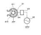
次に、上記実施形態におけるコイルシールド64内の電界の状態について補足的に説明する。図3は、図1のコイルシールド64内における電界の状態について説明した断面概略図である。
上述したように、コイルシールド64は高周波コイル61の断面形状と同心円周状の断面を有している。そして、コイルシールド64自体は、接地されている。従って、図3に示すように、高周波コイル61に供給された高周波電圧による電気力線610は、図2に示すように高周波コイル61の太さの中心点を中心として放射状に延びる状態となる。そして、高周波コイル61から放射される電界の等電位面611は、中心から同心円周状に広がる状態となる。このため、コイルシールド64内で高周波電界が乱されることなく誘起され、高周波通過用開口640から安定して高周波が放射され、イオン化空間に安定したプラズマを形成することができる。
【0039】
次に、好適な構成のシールドを有する別の実施形態について補足的に説明する。図4は、図1のコイルシールド64の好適な構成について説明する断面概略図である。
上述したように、コイルシールド64は、高周波コイル61の外側を覆うものであり、スパッタされて放出される高周波コイル61の材料が基板50に到達するのを遮蔽するものである。高周波コイル61から基板50へのスパッタ粒子の遮蔽ということを最も効果的にするには、コイルシールド64から高周波通過用開口640を通しては基板50上及びターゲット2の被スパッタ面上のいずれの点も見通せない構成にすることが好適である。
【0040】
図4を使用してより具体的に説明する。一例として、図面上右側に位置する高周波通過用開口640について説明する。図4に示すように、この高周波通過用開口640の下縁を通り高周波コイル61の上側の面に接する接線(以下、第一接線)641が、基板50の左側の縁より外側を通る場合、この高周波通過用開口640を通しては基板50上のいずれの点も見通せないことになる。尚、基板50は円形であることを想定している。
【0041】
また、この高周波通過用開口640の上縁を通り高周波コイル61の下側の面に接する接線(以下、第二接線)642が、ターゲット2の被スパッタ面の左側の縁より外側を通る場合、この高周波通過用開口640を通してはターゲット2の被スパッタ面上のいずれの点も見通せないことになる。尚、ターゲット2の被スパッタ面とは、ターゲットホルダー等に固定されるターゲット2の表面領域を除いて、スパッタ電極3によって専らスパッタされる表面領域を意味している。
【0042】
図4上で左側に位置する高周波通過用開口640も同様であり、第一接線641が基板50の右側の縁より外側を通り、第二接線642がターゲット2の被スパッタ面の右側の縁より外側を通る場合、この高周波通過用開口640を通しては基板50上及びターゲット2の被スパッタ面上のいずれの点も見通せないことになる。
【0043】
高周波通過用開口640の幾何学的な配置を上記のように構成することで、高周波コイル61から基板50へのスパッタ粒子の遮蔽という効果を最も良好に得ることができる。但し、上述した通り、高周波の通過効率の点からは高周波通過用開口640はできるだけ大きい方が良いので、第一接線641が基板50の縁に接し、第二接線642がターゲット2の被スパッタ面の縁に接するような臨界的な配置が採られる場合もある。
【0044】
次に、本願発明の第二の実施形態について説明する。図5は、本願発明の第二の実施形態に係るイオン化スパッタリング装置の要部の構成を説明する正面概略図である。
この第二の実施形態の装置では、基板50に作成する薄膜の材料であるターゲット2の材料と同一の材料で高周波コイル61が形成されている点と、高周波コイル61の外側には補助シールド65が設けられている点が大きな特徴点になっている。
【0045】
まず、高周波コイル61をターゲット2と同一材料とすることは、上述したスパッタされた高周波コイル61の材料による基板50の汚損という問題を第一の実施形態とは別な考え方によって解決するものである。つまり、高周波コイル61の材料が基板50に付着したとしても問題にならない材料で高周波コイル61を形成するという考え方である。具体的には、バリア膜を作成する場合、ターゲット2はチタン製であり、高周波コイル61も同様にチタン製とされる。
尚、高周波コイル61は経時的にスパッタされて消耗するので、交換容易な状態でスパッタチャンバー1内に取付けられていると好適である。
【0046】
高周波コイル61の外側の補助シールド65は、第一の実施形態のコイルシールド64とは若干目的が異なっている。高周波コイル61はターゲット2と同一材料であるので、高周波コイル61からのスパッタ粒子を遮蔽する必要性はこの第二の実施形態ではそれほどない。この補助シールド65の主な目的は、高周波コイル61の外側でのエネルギー供給を防止して、高周波コイル61の内側にプラズマを閉じ込めることである。
【0047】
即ち、この補助シールド65が無いと、高周波コイル61の外側にも高周波が放射され、高周波コイル61の外側に存在するガス分子にエネルギーを与えて放電を生じ、高周波コイル61の外側にもプラズマを形成してしまう。このため、プラズマは、高周波コイル61の内側から外側に広がって形成されてしまう。高周波コイル61の外側に形成されたプラズマは、ターゲットからのスパッタ粒子をイオン化させるのには殆ど役に立たない。このような不要な領域にプラズマが形成されると、その領域に存在する部材を不必要にスパッタする等の色々な問題を派生させる。しかしながら、本実施形態では、補助シールド65によって高周波コイル61の外側でのプラズマ形成が抑制されているので、このような問題は生じない。
【0048】
また、図4に示す補助シールド65は、図3に示すコイルシールド64と同様に、高周波コイル61の太さの中心と同心円周状の断面形状を有している。このため、補助シールド65の高周波コイル61を臨む表面が、高周波コイル61から放射される電界の等電位面に沿った形状になる。このため、高周波コイル61と補助シールド65との間の電界の分布は中心対称的なものになり、イオン化空間での安定した高周波電界の設定に貢献している。
【0049】
補助シールド65は、コイルシールド64と同様に、ステンレスやアルミニウム等の金属で形成され、電気的には接地されている。また、補助シールド65の表面をアルマイト処理したり、堆積膜の落下を防止する凹凸を設けたりすると良い点も同様である。
尚、前述した第一の実施形態におけるコイルシールド64も、この補助シールド65と同様の効果を有しているのは勿論である。また、この補助シールド65についても、コイルシールド64と同様に、高周波コイル61からのスパッタ粒子の遮蔽効果を持たせるようにしてもよい。
【0050】
次に、請求項7及び8の発明に対応した第三の実施形態について説明する。図6は、本願発明の第三の実施形態に係るイオン化スパッタリング装置の要部の構成を説明する正面概略図である。
この第三の実施形態の装置は、コイルシールド64が設けられている点は第一の実施形態と同様であるが、高周波コイル61がイオン化空間へのガス導入機能を有している点が大きく異なっている。即ち、第三の実施形態における高周波コイル61は、内部が中空になっており、イオン化空間を臨む内側の面にガス吹き出し穴612が均等に形成されている。
【0051】
高周波コイル61は、例えば内径6mm外径10mmのパイプ状の部材を螺旋状に形成したものである。ガス吹き出し穴612は、例えば直径0.2mm程度の円形で、20mm程度の間隔で設けることができる。尚、ガス吹き出し穴612をあまり大きくすると、ガス吹き出し穴612を通して高周波コイル61の内部にプラズマが進入する問題があるので、あまり大きくするべきではない。
【0052】
このような高周波コイル61は、ガス導入手段4の配管42に接続されている。具体的には、配管42から分岐するようにして補助配管47が設けられており、補助配管47に補助チャンバー内配管48が接続されている。そして、補助チャンバー内配管48の先端に高周波コイル61が接続されている。この結果、ガス分配器46から導入されるガスと同じガスが高周波コイル61からも導入されるようになっている。
【0053】
このような高周波コイル61の構成は、高周波エネルギーが多く供給される場所に多くのガスを供給することでプラズマ形成効率を高める作用を有している。即ち、高周波コイル61からは、内側のイオン化空間に高周波エネルギーが最も多く供給されるが、ガス分配器46のみの構成であると、ガス分配器46からイオン化空間までは距離があるので、イオン化空間に達する前にガスは拡散してしまい充分な量のガスが供給されない恐れがある。
一方、高周波コイル61のガス吹き出し穴612からガス供給を行うようにすると、イオン化空間はその目の前であるので、充分な量のガスが供給される。このため、プラズマの形成効率が高くなる。
【0054】
尚、スパッタ電極3へのガス供給については、ガス分配器46を用いずに高周波コイル61からのガス供給で足りる場合があり、この場合はガス分配器46及びチャンバー内配管45は省略される。
また、高周波コイル61を接続した補助配管47には、高周波コイル61に供給するガスの温度調節器49が設けられている。温度調節器49は、具体的にはガスを所定温度に冷却する冷却器である。
【0055】
高周波コイル61は、イオン化空間に形成されるプラズマからの電子衝撃や表面に流れる高周波電流に伴うジュール熱によって加熱される。高周波コイル61が限度以上に加熱されると、高周波コイル61に熱的な損傷が発生したり、高周波コイル61への膜堆積が促進されてしまう問題がある。
そこで、本実施形態では、高周波コイル61に供給するガスを温度調節器49によって所定温度に冷却し、ガスの冷却効果によって高周波コイル61の温度上昇を所定温度以下に抑えている。このため、熱的損傷や過剰な膜堆積等の問題が高周波コイル61に生じないようになっている。
【0056】
温度調節器49は、高周波コイル61の冷却以外の目的でも用いることができる。例えば、イオン化空間に供給するガスの温度を何らかの事情で温度調節する必要がある場合、温度調節器49が好適に使用される。
尚、この第三の実施形態における高周波コイル61についても、第二の実施形態と同様にターゲット2と同一材料とすることが可能である。また、コイルシールド64に代えて第二実施形態の補助シールド65を採用することも可能である。
【0057】
上記各実施形態では、イオン化手段6としては、高周波誘導結合型プラズマを形成してスパッタ粒子をイオン化する構成を採用したが、これ以外にも多くの構成が考えられる。例えば、プラズマを形成するものとしては、高周波容量結合型プラズマや直流二極放電プラズマ、電子サイクロトロン共鳴(ECR)プラズマ、ヘリコン波プラズマ等を形成するものが採用できる。また、イオン化空間に正イオンを照射してスパッタ粒子から電子を奪ってイオン化させるイオン源等も、イオン化手段6として採用できる。
【0058】
また、上記各実施形態では、イオン化したスパッタ粒子を基板50に引き出すための電界を設定するための電界設定手段7を使用しているが、このような電界設定手段7を設けなくともイオン化スパッタリングの効果が得られる場合がある。例えば、高周波コイル61が与える高周波電界によって加速されて効果的にイオンを基板50に入射させることが可能な場合があり、このような場合には電界設定手段7は不要とされる。
【0059】
さらに、高周波コイル61の構成としては、前述した螺旋状の他、リング状の部材のみからなる単巻コイルや、二本(又は三本以上)リング状の部材を上下に所定間隔をおいて配置してコネクティングロッドでつないだ構成等も、高周波コイル61の構成として採用できる。
尚、本願発明のスパッタリング装置は、各種半導体デバイスの他、液晶ディスプレイやその他の各種電子製品の製作に利用することができる。
【0060】
【発明の効果】
以上説明した通り、本願の請求項1の発明によれば、高周波コイルの外側にプラズマが不必要に形成されることによる問題が生じない。加えて、高周波通過用開口を通してプラズマがシールド内に拡散しないようにしたり、またはスパッタによって放出されたスパッタ粒子の殆どがコイルシールドに遮蔽されるようにしたりすることができる。
また、請求項2の発明によれば、上記効果に加え、シールド内の電界が中心対称的なものになり、イオン化空間に安定して高周波を放射させてイオン化を安定して行うことができるという効果が得られる。
また、請求項3の発明によれば、上記効果に加え、高周波コイルからのスパッタ粒子の遮蔽効果が高くなるという効果が得られる。
また、請求項4の発明によれば、上記効果に加え、高周波コイルからのスパッタ粒子の遮蔽効果が最も高くなるという効果が得られる。
また、請求項5の発明によれば、上記効果に加え、高周波コイルの表面の堆積膜の落下により基板が汚損されるのが防止される。
また、請求項6の発明によれば、上記効果に加え、高周波コイルがスパッタされ、高周波コイルの材料が基板に付着したとしても問題にはならないという効果が得られる。
また、請求項7の発明によれば、上記効果に加え、イオン化スパッタの効果をさらに向上させることができる。
また、請求項8の発明によれば、上記効果に加え、高周波エネルギーが多く供給されるイオン化空間に多くのガスを供給できるので、プラズマ形成効率を高めることが可能となる。
また、請求項9の発明によれば、上記効果に加え、高周波コイルを所定温度に冷却することで高周波コイルの熱的損傷や過剰な膜堆積等の問題を防止するような温度調節を容易に行うことができる。
【図面の簡単な説明】
【図1】本願発明の第一の実施形態のスパッタリング装置の構成を説明する正面概略図である。
【図2】図1の装置に使用されたコイルシールド64の具体的寸法の説明図である。
【図3】図1のコイルシールド64内における電界の状態について説明した断面概略図である。
【図4】図1のコイルシールド64の好適な構成について説明する断面概略図である。
【図5】本願発明の第二の実施形態に係るイオン化スパッタリング装置の要部の構成を説明する正面概略図である。
【図6】本願発明の第三の実施形態に係るイオン化スパッタリング装置の要部の構成を説明する正面概略図である。
【符号の説明】
1 スパッタチャンバー
11 排気系
2 ターゲット
3 スパッタ電極
4 ガス導入手段
41 ガスボンベ
42 配管
43 バルブ
44 流量調整器
45 チャンバー内配管
46 ガス分配器
47 補助配管
48 補助チャンバー内配管
49 温度調節器
5 基板ホルダー
50 基板
6 イオン化手段
61 高周波コイル
62 高周波電源
63 整合器
64 コイルシールド
65 補助シールド
7 電界設定手段
71 基板バイアス用高周波電源[0001]
BACKGROUND OF THE INVENTION
The present invention relates to a sputtering apparatus used for manufacturing various semiconductor devices, and particularly to an ionization sputtering apparatus having a function of ionizing sputtered particles.
[0002]
[Prior art]
In semiconductor devices such as various memories and logics, a sputtering process is used when forming various wiring films and creating barrier films for preventing mutual diffusion of different layers, and sputtering apparatuses are frequently used. Although there are various characteristics required for such a sputtering apparatus, it has recently been strongly demanded that the inner surface of a hole formed in a substrate can be coated with good coverage.
[0003]
Specifically, for example, in the case of a barrier film, an improvement in the bottom coverage ratio, which is the ratio of the film formation rate on the bottom surface of the hole with respect to the peripheral surface of the hole, has recently been particularly strongly demanded. This is because the aspect ratio (ratio of the depth of the hole to the size of the hole opening) of the hole such as a contact hole has been increasing year by year due to the increase in the degree of integration. This is because the conventional sputtering technique often cannot form a film with good bottom coverage. When the bottom coverage rate decreases, the barrier film becomes thin on the bottom surface of the hole, which may cause a fatal defect in device characteristics such as a junction leak.
[0004]
As sputtering techniques for improving the bottom coverage rate, techniques such as collimated sputtering and low-pressure remote sputtering have been developed so far. Although a detailed description of these methods is omitted, each of them is an attempt to make a lot of neutral sputtered particles enter the substrate perpendicularly.
[0005]
However, in collimated sputtering, sputtered particles accumulate on the collimator and become lost, so there is a problem that the film formation speed decreases. In low pressure remote sputtering, the pressure is lowered and the distance between the target and the substrate is increased. Therefore, there is a problem that the film forming speed is essentially lowered. Because of these problems, it is predicted that the limit is 64 megabits for collimated sputtering and the first generation of 256 megabits for low-pressure remote sputtering. A search for a new technique is underway.
[0006]
Recently, it has been considered that ionization sputtering is a promising technique for meeting such demands. Ionized sputtering is a technique in which sputtered particles emitted from a target are ionized and the sputtered particles efficiently reach the holes by the action of ions. It has been confirmed that ionized sputtering can provide a much higher bottom coverage than collimated sputtering or low-pressure remote sputtering.
[0007]
As a typical configuration of ionized sputtering, plasma is formed on the flight path of sputtered particles between the substrate and the target, and the sputtered particles are ionized when passing through the plasma. As the plasma, inductively coupled plasma is usually formed. Specifically, a high frequency coil is provided so as to surround a space for ionization (hereinafter referred to as ionization space) on the flight path, and a predetermined high frequency is supplied to the high frequency coil to form plasma inside the high frequency coil. To. A high frequency current flows in the plasma, and the plasma and the high frequency coil are inductively coupled. For this reason, it is called inductively coupled plasma.
[0008]
[Problems to be solved by the invention]
However, according to the inventors' investigation, it has been found that the above-described configuration of ionized sputtering has the following problems.
First of all, in order to set a high-frequency electric field of sufficient strength in the ionization space, the high-frequency coil is usually arranged inside the sputtering chamber, but the high-frequency coil is sputtered by plasma, and the sputtered high-frequency coil material is As a result of reaching the substrate, there is a problem of fouling the substrate.
Second, since gas diffuses in the sputtering chamber, plasma may be formed outside the high-frequency coil, and the plasma formed in such a place is not only unnecessary for ionization. In some cases, the member disposed at the place may be damaged.
Third, when plasma is formed, it also serves as a gas introduction means for introducing gas for sputter discharge. However, the optimum gas introduction for spatter discharge and ionization plasma formation is optimal. Different from the configuration. For this reason, gas cannot be supplied efficiently for plasma formation, and plasma formation efficiency is poor.
The invention of the present application has been made in order to solve such problems, and provides a practical ionization sputtering apparatus that solves such problems of ionization sputtering and is effective in the production of next-generation devices. The purpose is that.
[0009]
[Means for Solving the Problems]
In order to solve the above-mentioned problems, an invention according to claim 1 of the present application is directed to a sputtering chamber provided with an exhaust system, a target provided in the sputtering chamber, a sputtering electrode for sputtering the target, and a predetermined amount in the sputtering chamber. An ionization sputtering apparatus comprising: a gas introduction unit that introduces a gas; an ionization unit that ionizes sputtered particles released from a target by sputtering; and a substrate holder that holds the substrate at a position where the ionized sputtered particles are incident. ,
The ionization means includes a high frequency coil provided in the sputtering chamber so as to surround the ionization space between the target and the substrate holder, and a high frequency inductively coupled plasma is supplied to the ionization space by supplying a predetermined high frequency to the high frequency coil. It consists of a high-frequency power supply to be formed,
On the outside of the high-frequency coil, there is a shield for confining plasma inside the high-frequency coil,
The shield is formed of a metal member and is electrically grounded.The high-frequency coil extends in the same direction, and when viewed in cross-section, each part of the high-frequency coil is surrounded and covered from the outside,It has a shape with an opening for high-frequency passage so that high-frequency radiation is emitted toward the ionization space inside.
The high-frequency passage opening is a slit formed over the entire length of the high-frequency coil.It has the structure of.
In order to solve the above problem, the invention according to claim 2 is the configuration according to claim 1, wherein the surface of the shield facing the high frequency coil is along the equipotential surface of the electric field radiated from the high frequency coil. It has the structure of being formed so as to have a shape.
Moreover, in order to solve the said subject, a claim3The invention described is the above claim.1 or 2In the configuration ofThe shield is from a high frequency coilIt has a configuration in which any point on the substrate cannot be seen through the high-frequency passage opening.
Moreover, in order to solve the said subject, a claim4The invention described is the above claim.1 or 2In the configuration ofThe shield is from a high frequency coilThrough the high-frequency passage opening, there is a configuration in which neither point on the substrate nor the target sputtering surface can be seen.
Moreover, in order to solve the said subject, a claim5The invention described is the above-mentioned claims 1 to4In any one of the configurations, the inner surface of the shield has a configuration in which unevenness that prevents the deposited film on the inner surface from dropping is provided.
Moreover, in order to solve the said subject, a claim6The invention described is the above-mentioned claims 1 to5In any one of the configurations, the high-frequency coil has a configuration in which the high-frequency coil is formed of the same material as a target material that is a material of a thin film formed on a substrate.
Moreover, in order to solve the said subject, a claim7The invention described is the above-mentioned claims 1 to6In any configuration, an electric field setting unit that sets an electric field in a direction perpendicular to the substrate in order to draw the ionized sputtered particles into the substrate is provided.
Moreover, in order to solve the said subject, a claim8The invention described is the above-mentioned claims 1 to7In any of the configurations, the high-frequency coil has a hollow inside, and gas blowing holes are uniformly formed on an inner surface facing the ionization space, and a pipe in the auxiliary chamber of the gas introduction unit is connected to the gas coil. It has a configuration in which a predetermined gas can be introduced into the ionization space from the blowing hole.
Moreover, in order to solve the said subject, a claim9The invention described is the above claim.8In the configuration, the gas introduction means includes a temperature controller that maintains a temperature of a gas supplied to the high-frequency coil at a predetermined temperature, and the temperature of the high-frequency coil can be adjusted. .
[0010]
DETAILED DESCRIPTION OF THE INVENTION
Embodiments of the present invention will be described below.First, about the first embodimentexplain. FIG. 1 is a schematic front view illustrating the configuration of the sputtering apparatus according to the first embodiment of the present invention.
As shown in FIG. 1, the sputtering apparatus of this embodiment includes a sputtering chamber 1 having an exhaust system 11, a target 2 provided in the sputtering chamber 1, a sputtering
[0011]
First, the sputter chamber 1 is an airtight container provided with a gate valve (not shown). The sputter chamber 1 is made of metal such as stainless steel and is electrically grounded.
The exhaust system 11 is composed of a multistage vacuum exhaust system equipped with a turbo molecular pump, a diffusion pump, and the like.-8-10-9Exhaust is possible to about Torr. The exhaust system 11 includes an exhaust speed regulator (not shown) such as a variable orifice, and can adjust the exhaust speed.
[0012]
The target 2 has a disk shape with a thickness of about 6 mm and a diameter of about 300 mm, for example, and is attached to the
The
The
[0013]
The gas introducing means 4 includes a
The
[0014]
In the present embodiment, the ionization means 6 that forms inductively coupled high-frequency plasma in the titanium flight path from the target 2 to the
[0015]
The
[0016]
The high
[0017]
When the sputtered particles emitted from the target 2 pass through the plasma P, they collide with electrons in the plasma P and are ionized. The ionized sputtered particles are accelerated by an electric field described later and reach the
[0018]
The substrate holder 5 is configured to hold the
[0019]
In this embodiment, the electric field setting means 7 applies a predetermined high frequency voltage to the substrate holder 5 to give a negative bias voltage to the
[0020]
The substrate bias high-frequency power supply 71 has, for example, a frequency of about 13.56 MHz and an output of about 300 W. When a high frequency voltage is applied to the
[0021]
The state where the substrate bias voltage is applied is the same as the cathode sheath region in the case where plasma is formed by DC bipolar discharge, and an electric field having a potential gradient that decreases toward the
[0022]
The substrate holder 5 is formed of the same metal material as the target 2 when the target 2 is a metal, and a heat-resistant metal such as stainless steel when the target 2 is a dielectric. In any case, the substrate holder 5 is made of metal, and therefore there is no electric field in principle in the mounting surface of the substrate holder 5. Therefore, the extraction electric field is an electric field in a direction perpendicular to the
[0023]
Next, the configuration of the
[0024]
As shown in FIG. 1, the
[0025]
An
[0026]
A specific dimension example of the
[0027]
The selection of the width d3 of the high-
[0028]
That is, when d3 increases, plasma diffuses in the
[0029]
Therefore, in consideration of such points, a value as large as possible should be given to d3 within a range in which plasma does not diffuse into the
[0030]
Such a
[0031]
Further, on the inner surface of the
[0032]
Next, operation | movement of the ionization sputtering apparatus of this embodiment is demonstrated using FIG.
The
[0033]
The inside of the sputter chamber 1 is maintained at, for example, about 30 to 40 mTorr by controlling the exhaust speed regulator of the exhaust system 11, and the
[0034]
At the same time, the ionization means 6 is also operated, a high frequency voltage is applied to the
[0035]
The target 2 is sputtered by the sputter discharge, and the sputtered titanium flies toward the
When the film is formed with a predetermined thickness, the operations of the electric field setting means 7, ionization means 6, sputter
[0036]
In the above operation, the surface of the high-
[0037]
Even when such a grounded
[0038]
next,State of electric field in
As described above, the
[0039]
next,Another with a shield of suitable configurationThe embodiment will be supplementarily described. FIG. 4 is a schematic cross-sectional view illustrating a preferred configuration of the
As described above, the
[0040]
This will be described more specifically with reference to FIG. As an example, the high-
[0041]
Further, when a tangent line (hereinafter referred to as a second tangent line) 642 that passes through the upper edge of the high
[0042]
The same applies to the high-
[0043]
By configuring the geometrical arrangement of the high-
[0044]
next,Second embodiment of the present inventionWill be described. FIG. 5 is a schematic front view illustrating the configuration of the main part of an ionization sputtering apparatus according to the second embodiment of the present invention.
In the apparatus of the second embodiment, the
[0045]
First, using the same material as that of the target 2 for the high-
Since the high-
[0046]
The
[0047]
In other words, without this
[0048]
Further, the
[0049]
Similar to the
Of course, the
[0050]
Next, a third embodiment corresponding to the seventh and eighth aspects of the invention will be described. FIG. 6 is a schematic front view illustrating the configuration of the main part of an ionization sputtering apparatus according to the third embodiment of the present invention.
The apparatus of the third embodiment is the same as the first embodiment in that the
[0051]
The
[0052]
Such a
[0053]
Such a configuration of the high-
On the other hand, when gas is supplied from the
[0054]
The gas supply to the
The
[0055]
The high-
Therefore, in the present embodiment, the gas supplied to the
[0056]
The
The high-
[0057]
In each of the above embodiments, the ionization means 6 employs a configuration in which high-frequency inductively coupled plasma is formed to ionize the sputtered particles, but many other configurations are conceivable. For example, a plasma can be formed by using a high frequency capacitively coupled plasma, a DC bipolar discharge plasma, an electron cyclotron resonance (ECR) plasma, a helicon wave plasma, or the like. An ion source or the like that irradiates positive ions to the ionization space to take electrons from the sputtered particles and ionize them can be used as the ionization means 6.
[0058]
In each of the above embodiments, the electric field setting means 7 for setting an electric field for extracting ionized sputtered particles to the
[0059]
Further, as the configuration of the high-
In addition, the sputtering apparatus of this invention can be utilized for manufacture of a liquid crystal display and other various electronic products besides various semiconductor devices.
[0060]
【The invention's effect】
As explained above,Claim 1According to this invention, there is no problem caused by unnecessary formation of plasma outside the high frequency coil. In addition, plasma does not diffuse into the shield through the high-frequency passage opening.Alternatively, most of the sputtered particles released by sputtering can be shielded by the coil shield.
Claims2According to the invention, in addition to the above effect, the electric field in the shield becomes centrally symmetric, and an effect is obtained that ionization can be stably performed by radiating a high frequency stably to the ionization space.
Claims3According to the invention, in addition to the above effect, the effect of increasing the shielding effect of the sputtered particles from the high frequency coil can be obtained.
Claims4According to the invention, in addition to the above-described effect, an effect that the shielding effect of the sputtered particles from the high-frequency coil becomes the highest can be obtained.
Claims5According to the invention, in addition to the above-described effect, the substrate is prevented from being soiled by the fall of the deposited film on the surface of the high-frequency coil.
Claims6According to the invention, in addition to the above effect, there is an effect that even if the high frequency coil is sputtered and the material of the high frequency coil adheres to the substrate, there is no problem.
Claims7According to the invention, in addition to the above effects, the effect of ionization sputtering can be further improved.
Claims8According to the invention, in addition to the above effects, a large amount of gas can be supplied to the ionization space where a large amount of high-frequency energy is supplied, so that the plasma forming efficiency can be increased.
Claims9According to the invention, in addition to the above effect, the high-frequency coil can be easily adjusted to a temperature so as to prevent problems such as thermal damage and excessive film deposition by cooling the high-frequency coil to a predetermined temperature.
[Brief description of the drawings]
FIG. 1 is a schematic front view illustrating the configuration of a sputtering apparatus according to a first embodiment of the present invention.
FIG. 2 is an explanatory diagram of specific dimensions of a
3 is a schematic cross-sectional view illustrating the state of an electric field in
4 is a schematic cross-sectional view illustrating a preferred configuration of the
FIG. 5 is a schematic front view illustrating a configuration of a main part of an ionization sputtering apparatus according to a second embodiment of the present invention.
FIG. 6 is a schematic front view illustrating the configuration of the main part of an ionization sputtering apparatus according to a third embodiment of the present invention.
[Explanation of symbols]
1 Sputter chamber
11 Exhaust system
2 Target
3 Sputter electrode
4 Gas introduction means
41 Gas cylinder
42 Piping
43 Valve
44 Flow controller
45 Piping in chamber
46 Gas distributor
47 Auxiliary piping
48 Piping in auxiliary chamber
49 Temperature controller
5 Board holder
50 substrates
6 Ionization means
61 high frequency coil
62 High frequency power supply
63 Matching device
64 Coil shield
65 Auxiliary shield
7 Electric field setting means
71 High frequency power supply for substrate bias
Claims (9)
Translated fromJapanese前記イオン化手段は、ターゲットと基板ホルダーとの間のイオン化空間を取り囲むようにスパッタチャンバー内に設けられた高周波コイルと、この高周波コイルに所定の高周波を供給してイオン化空間に高周波誘導結合型プラズマを形成する高周波電源とから構成されており、
当該高周波コイルの外側には、高周波コイルの内側にプラズマを閉じ込めるシールドが設けられており、
このシールドは、金属製の部材で形成され電気的に接地されているとともに、このシールドは、高周波コイルが延びる方向に同様に延びるものであって、断面で見ると、高周波コイルの各部をそれぞれ外側から取り囲んで覆うとともに、内側にイオン化空間に向けて高周波が放射されるよう高周波通過用開口を設けた形状であり、
高周波通過用開口は、高周波コイルの全長にわたって形成されたスリットであることを特徴とするイオン化スパッタリング装置。Sputter chamber equipped with an exhaust system, target provided in the sputter chamber, sputter electrode for sputtering the target, gas introducing means for introducing a predetermined gas into the sputter chamber, and sputter released from the target by sputtering An ionization sputtering apparatus comprising ionization means for ionizing particles and a substrate holder for holding a substrate at a position where ionized sputtered particles are incident,
The ionization means includes a high frequency coil provided in the sputtering chamber so as to surround the ionization space between the target and the substrate holder, and a high frequency inductively coupled plasma is supplied to the ionization space by supplying a predetermined high frequency to the high frequency coil. It consists of a high-frequency power supply to be formed,
On the outside of the high-frequency coil, there is a shield for confining plasma inside the high-frequency coil,
This shield is formed of a metal member and is electrically grounded, and this shieldextends in the same way in the direction in which the high-frequency coil extends. with the surrounding covering of a shape which high frequency is provided a high-frequency passage opening so as to be radiated toward the ionization space inside,
The high frequency passage opening is a slit formed over the entire length of the high frequency coil .
Priority Applications (3)
| Application Number | Priority Date | Filing Date | Title |
|---|---|---|---|
| JP11190297AJP3846970B2 (en) | 1997-04-14 | 1997-04-14 | Ionization sputtering equipment |
| US09/022,623US5968327A (en) | 1997-04-14 | 1998-02-12 | Ionizing sputter device using a coil shield |
| KR1019980005372AKR100299782B1 (en) | 1997-04-14 | 1998-02-20 | Ionizing sputtering device |
Applications Claiming Priority (1)
| Application Number | Priority Date | Filing Date | Title |
|---|---|---|---|
| JP11190297AJP3846970B2 (en) | 1997-04-14 | 1997-04-14 | Ionization sputtering equipment |
Publications (2)
| Publication Number | Publication Date |
|---|---|
| JPH10289887A JPH10289887A (en) | 1998-10-27 |
| JP3846970B2true JP3846970B2 (en) | 2006-11-15 |
Family
ID=14572998
Family Applications (1)
| Application Number | Title | Priority Date | Filing Date |
|---|---|---|---|
| JP11190297AExpired - Fee RelatedJP3846970B2 (en) | 1997-04-14 | 1997-04-14 | Ionization sputtering equipment |
Country Status (3)
| Country | Link |
|---|---|
| US (1) | US5968327A (en) |
| JP (1) | JP3846970B2 (en) |
| KR (1) | KR100299782B1 (en) |
Families Citing this family (44)
| Publication number | Priority date | Publication date | Assignee | Title |
|---|---|---|---|---|
| US6429120B1 (en)* | 2000-01-18 | 2002-08-06 | Micron Technology, Inc. | Methods and apparatus for making integrated-circuit wiring from copper, silver, gold, and other metals |
| JP4355036B2 (en)* | 1997-03-18 | 2009-10-28 | キヤノンアネルバ株式会社 | Ionization sputtering equipment |
| US6210539B1 (en)* | 1997-05-14 | 2001-04-03 | Applied Materials, Inc. | Method and apparatus for producing a uniform density plasma above a substrate |
| US6287977B1 (en) | 1998-07-31 | 2001-09-11 | Applied Materials, Inc. | Method and apparatus for forming improved metal interconnects |
| US6165567A (en)* | 1999-04-12 | 2000-12-26 | Motorola, Inc. | Process of forming a semiconductor device |
| US7349223B2 (en) | 2000-05-23 | 2008-03-25 | Nanonexus, Inc. | Enhanced compliant probe card systems having improved planarity |
| US7247035B2 (en) | 2000-06-20 | 2007-07-24 | Nanonexus, Inc. | Enhanced stress metal spring contactor |
| US6812718B1 (en) | 1999-05-27 | 2004-11-02 | Nanonexus, Inc. | Massively parallel interface for electronic circuits |
| US7382142B2 (en) | 2000-05-23 | 2008-06-03 | Nanonexus, Inc. | High density interconnect system having rapid fabrication cycle |
| US6238532B1 (en)* | 1999-10-29 | 2001-05-29 | International Business Machines Corporation | Radio-frequency coil for use in an ionized physical vapor deposition apparatus |
| US6350353B2 (en)* | 1999-11-24 | 2002-02-26 | Applied Materials, Inc. | Alternate steps of IMP and sputtering process to improve sidewall coverage |
| JP3610289B2 (en)* | 2000-04-28 | 2005-01-12 | キヤノン株式会社 | Sputtering apparatus and sputtering method |
| US6551471B1 (en) | 1999-11-30 | 2003-04-22 | Canon Kabushiki Kaisha | Ionization film-forming method and apparatus |
| US6344419B1 (en) | 1999-12-03 | 2002-02-05 | Applied Materials, Inc. | Pulsed-mode RF bias for sidewall coverage improvement |
| US6420262B1 (en) | 2000-01-18 | 2002-07-16 | Micron Technology, Inc. | Structures and methods to enhance copper metallization |
| US7211512B1 (en) | 2000-01-18 | 2007-05-01 | Micron Technology, Inc. | Selective electroless-plated copper metallization |
| US7262130B1 (en) | 2000-01-18 | 2007-08-28 | Micron Technology, Inc. | Methods for making integrated-circuit wiring from copper, silver, gold, and other metals |
| JP3297415B2 (en)* | 2000-02-09 | 2002-07-02 | 株式会社半導体先端テクノロジーズ | Method for manufacturing semiconductor device |
| US6627056B2 (en)* | 2000-02-16 | 2003-09-30 | Applied Materials, Inc. | Method and apparatus for ionized plasma deposition |
| TW584905B (en)* | 2000-02-25 | 2004-04-21 | Tokyo Electron Ltd | Method and apparatus for depositing films |
| US7579848B2 (en) | 2000-05-23 | 2009-08-25 | Nanonexus, Inc. | High density interconnect system for IC packages and interconnect assemblies |
| US7952373B2 (en) | 2000-05-23 | 2011-05-31 | Verigy (Singapore) Pte. Ltd. | Construction structures and manufacturing processes for integrated circuit wafer probe card assemblies |
| US6554979B2 (en) | 2000-06-05 | 2003-04-29 | Applied Materials, Inc. | Method and apparatus for bias deposition in a modulating electric field |
| US6746591B2 (en) | 2001-10-16 | 2004-06-08 | Applied Materials Inc. | ECP gap fill by modulating the voltate on the seed layer to increase copper concentration inside feature |
| JP4078084B2 (en)* | 2002-01-28 | 2008-04-23 | キヤノン株式会社 | Ionized film forming method and apparatus |
| US6946054B2 (en) | 2002-02-22 | 2005-09-20 | Tokyo Electron Limited | Modified transfer function deposition baffles and high density plasma ignition therewith in semiconductor processing |
| US7147759B2 (en)* | 2002-09-30 | 2006-12-12 | Zond, Inc. | High-power pulsed magnetron sputtering |
| US6896773B2 (en)* | 2002-11-14 | 2005-05-24 | Zond, Inc. | High deposition rate sputtering |
| US20060249370A1 (en)* | 2003-09-15 | 2006-11-09 | Makoto Nagashima | Back-biased face target sputtering based liquid crystal display device |
| US20050103620A1 (en)* | 2003-11-19 | 2005-05-19 | Zond, Inc. | Plasma source with segmented magnetron cathode |
| US9771648B2 (en)* | 2004-08-13 | 2017-09-26 | Zond, Inc. | Method of ionized physical vapor deposition sputter coating high aspect-ratio structures |
| US9123508B2 (en)* | 2004-02-22 | 2015-09-01 | Zond, Llc | Apparatus and method for sputtering hard coatings |
| EP1803142A1 (en)* | 2004-09-24 | 2007-07-04 | Zond, Inc. | Apparatus for generating high-current electrical discharges |
| JP4830421B2 (en)* | 2005-06-28 | 2011-12-07 | 東京エレクトロン株式会社 | Metal film forming method and film forming apparatus |
| US20070012557A1 (en)* | 2005-07-13 | 2007-01-18 | Applied Materials, Inc | Low voltage sputtering for large area substrates |
| US20070205096A1 (en)* | 2006-03-06 | 2007-09-06 | Makoto Nagashima | Magnetron based wafer processing |
| US8454810B2 (en) | 2006-07-14 | 2013-06-04 | 4D-S Pty Ltd. | Dual hexagonal shaped plasma source |
| US8308915B2 (en)* | 2006-09-14 | 2012-11-13 | 4D-S Pty Ltd. | Systems and methods for magnetron deposition |
| TWI386502B (en)* | 2007-05-25 | 2013-02-21 | Hon Hai Prec Ind Co Ltd | Holding device for sputtering |
| EP2345750B1 (en) | 2008-08-28 | 2019-01-02 | EMD Corporation | Thin film-forming sputtering systems |
| KR20100120336A (en)* | 2009-05-06 | 2010-11-16 | 인제대학교 산학협력단 | Plasma processing apparatus having a diffusion pump |
| US9398680B2 (en) | 2010-12-03 | 2016-07-19 | Lam Research Corporation | Immersible plasma coil assembly and method for operating the same |
| KR102592144B1 (en)* | 2015-12-15 | 2023-10-20 | 삼성전자주식회사 | Sputtering apparatus for conformal deposition and method of forming conformal electrolyte film of three dimensional secondary battery |
| KR102654487B1 (en)* | 2021-12-29 | 2024-04-05 | 피에스케이 주식회사 | Plasma generation unit, and apparatus for treating substrate with the same |
Family Cites Families (11)
| Publication number | Priority date | Publication date | Assignee | Title |
|---|---|---|---|---|
| WO1992007969A1 (en)* | 1990-10-31 | 1992-05-14 | International Business Machines Corporation | Apparatus for depositing material into high aspect ratio holes |
| US5178739A (en)* | 1990-10-31 | 1993-01-12 | International Business Machines Corporation | Apparatus for depositing material into high aspect ratio holes |
| US5397962A (en)* | 1992-06-29 | 1995-03-14 | Texas Instruments Incorporated | Source and method for generating high-density plasma with inductive power coupling |
| US5431799A (en)* | 1993-10-29 | 1995-07-11 | Applied Materials, Inc. | Collimation hardware with RF bias rings to enhance sputter and/or substrate cavity ion generation efficiency |
| JPH07268624A (en)* | 1994-03-25 | 1995-10-17 | Tatsuo Asamaki | Electric discharge device |
| US5545978A (en)* | 1994-06-27 | 1996-08-13 | International Business Machines Corporation | Bandgap reference generator having regulation and kick-start circuits |
| US5763851A (en)* | 1995-11-27 | 1998-06-09 | Applied Materials, Inc. | Slotted RF coil shield for plasma deposition system |
| US5800619A (en)* | 1996-06-10 | 1998-09-01 | Lam Research Corporation | Vacuum plasma processor having coil with minimum magnetic field in its center |
| US5707398A (en)* | 1996-11-12 | 1998-01-13 | Pacesetter, Inc. | Automatic determination of optimum electrode configuration for a cardiac stimulator |
| US5800688A (en)* | 1997-04-21 | 1998-09-01 | Tokyo Electron Limited | Apparatus for ionized sputtering |
| US5903106A (en)* | 1997-11-17 | 1999-05-11 | Wj Semiconductor Equipment Group, Inc. | Plasma generating apparatus having an electrostatic shield |
- 1997
- 1997-04-14JPJP11190297Apatent/JP3846970B2/ennot_activeExpired - Fee Related
- 1998
- 1998-02-12USUS09/022,623patent/US5968327A/ennot_activeExpired - Lifetime
- 1998-02-20KRKR1019980005372Apatent/KR100299782B1/ennot_activeExpired - Fee Related
Also Published As
| Publication number | Publication date |
|---|---|
| US5968327A (en) | 1999-10-19 |
| JPH10289887A (en) | 1998-10-27 |
| KR100299782B1 (en) | 2001-09-22 |
| KR19980079752A (en) | 1998-11-25 |
Similar Documents
| Publication | Publication Date | Title |
|---|---|---|
| JP3846970B2 (en) | Ionization sputtering equipment | |
| KR100659828B1 (en) | Ionized Physical Vapor Deposition Method and Apparatus | |
| CN1228810C (en) | Method and appts. for ionized sputtering of materials | |
| US6080287A (en) | Method and apparatus for ionized physical vapor deposition | |
| KR101001743B1 (en) | Ionization Physical Vapor Deposition System Using Helical Self-Resonant Coil | |
| US5800688A (en) | Apparatus for ionized sputtering | |
| US6197165B1 (en) | Method and apparatus for ionized physical vapor deposition | |
| US5961793A (en) | Method of reducing generation of particulate matter in a sputtering chamber | |
| US6514390B1 (en) | Method to eliminate coil sputtering in an ICP source | |
| JP3737363B2 (en) | Physical vapor treatment of surfaces with non-uniformity compensation | |
| KR19980033213A (en) | How to reduce the generation of particulate matter in the sputtering chamber | |
| JP2002537488A (en) | Apparatus with plasma deposition method and magnetic bucket and concentric plasma and material source | |
| JP4588212B2 (en) | Sputtering apparatus comprising a coil having overlapping ends | |
| JP2002520492A (en) | Feedthrough overlapping coil | |
| CN116752109B (en) | Physical vapor deposition equipment, deposition process and etching process | |
| EP0544831B1 (en) | Sputtering apparatus and sputtering method of improving ion flux distribution uniformity on a substrate | |
| JP2002512310A (en) | Small diameter coils enhance the uniformity of metal films formed by inductively coupled plasma deposition | |
| WO2000003055A1 (en) | Shield for ionized physical vapor deposition apparatus | |
| JP6489998B2 (en) | Plasma generator and plasma sputtering apparatus | |
| JP2832256B2 (en) | Plasma deposition equipment | |
| KR100397751B1 (en) | Magnetron apparatus for ferro-magnetic materials | |
| KR20000009541U (en) | Sputtering Device of Semiconductor Element |
Legal Events
| Date | Code | Title | Description |
|---|---|---|---|
| A621 | Written request for application examination | Free format text:JAPANESE INTERMEDIATE CODE: A621 Effective date:20040413 | |
| A977 | Report on retrieval | Free format text:JAPANESE INTERMEDIATE CODE: A971007 Effective date:20051108 | |
| A131 | Notification of reasons for refusal | Free format text:JAPANESE INTERMEDIATE CODE: A131 Effective date:20051115 | |
| A521 | Written amendment | Free format text:JAPANESE INTERMEDIATE CODE: A523 Effective date:20060116 | |
| A131 | Notification of reasons for refusal | Free format text:JAPANESE INTERMEDIATE CODE: A131 Effective date:20060228 | |
| A521 | Written amendment | Free format text:JAPANESE INTERMEDIATE CODE: A523 Effective date:20060429 | |
| A131 | Notification of reasons for refusal | Free format text:JAPANESE INTERMEDIATE CODE: A131 Effective date:20060627 | |
| A521 | Written amendment | Free format text:JAPANESE INTERMEDIATE CODE: A523 Effective date:20060721 | |
| TRDD | Decision of grant or rejection written | ||
| A01 | Written decision to grant a patent or to grant a registration (utility model) | Free format text:JAPANESE INTERMEDIATE CODE: A01 Effective date:20060815 | |
| A61 | First payment of annual fees (during grant procedure) | Free format text:JAPANESE INTERMEDIATE CODE: A61 Effective date:20060822 | |
| R150 | Certificate of patent or registration of utility model | Free format text:JAPANESE INTERMEDIATE CODE: R150 | |
| FPAY | Renewal fee payment (event date is renewal date of database) | Free format text:PAYMENT UNTIL: 20090901 Year of fee payment:3 | |
| S531 | Written request for registration of change of domicile | Free format text:JAPANESE INTERMEDIATE CODE: R313531 | |
| FPAY | Renewal fee payment (event date is renewal date of database) | Free format text:PAYMENT UNTIL: 20090901 Year of fee payment:3 | |
| R350 | Written notification of registration of transfer | Free format text:JAPANESE INTERMEDIATE CODE: R350 | |
| FPAY | Renewal fee payment (event date is renewal date of database) | Free format text:PAYMENT UNTIL: 20090901 Year of fee payment:3 | |
| FPAY | Renewal fee payment (event date is renewal date of database) | Free format text:PAYMENT UNTIL: 20100901 Year of fee payment:4 | |
| FPAY | Renewal fee payment (event date is renewal date of database) | Free format text:PAYMENT UNTIL: 20100901 Year of fee payment:4 | |
| FPAY | Renewal fee payment (event date is renewal date of database) | Free format text:PAYMENT UNTIL: 20110901 Year of fee payment:5 | |
| FPAY | Renewal fee payment (event date is renewal date of database) | Free format text:PAYMENT UNTIL: 20110901 Year of fee payment:5 | |
| FPAY | Renewal fee payment (event date is renewal date of database) | Free format text:PAYMENT UNTIL: 20120901 Year of fee payment:6 | |
| FPAY | Renewal fee payment (event date is renewal date of database) | Free format text:PAYMENT UNTIL: 20120901 Year of fee payment:6 | |
| FPAY | Renewal fee payment (event date is renewal date of database) | Free format text:PAYMENT UNTIL: 20130901 Year of fee payment:7 | |
| R250 | Receipt of annual fees | Free format text:JAPANESE INTERMEDIATE CODE: R250 | |
| R250 | Receipt of annual fees | Free format text:JAPANESE INTERMEDIATE CODE: R250 | |
| R250 | Receipt of annual fees | Free format text:JAPANESE INTERMEDIATE CODE: R250 | |
| LAPS | Cancellation because of no payment of annual fees |