JP3840253B2 - Optical element and manufacturing method thereof - Google Patents
Optical element and manufacturing method thereofDownload PDFInfo
- Publication number
- JP3840253B2 JP3840253B2JP2005330273AJP2005330273AJP3840253B2JP 3840253 B2JP3840253 B2JP 3840253B2JP 2005330273 AJP2005330273 AJP 2005330273AJP 2005330273 AJP2005330273 AJP 2005330273AJP 3840253 B2JP3840253 B2JP 3840253B2
- Authority
- JP
- Japan
- Prior art keywords
- layer
- optical element
- reflecting mirror
- nitride semiconductor
- dbr
- Prior art date
- Legal status (The legal status is an assumption and is not a legal conclusion. Google has not performed a legal analysis and makes no representation as to the accuracy of the status listed.)
- Expired - Fee Related
Links
Images


Landscapes
- Drying Of Semiconductors (AREA)
- Semiconductor Lasers (AREA)
Description
Translated fromJapanese本発明は、光素子及びそれらの製造方法に関し、特に、反射特性が顕著に優れた分布ブラッグ反射鏡を備えた光素子及びそれらの製造方法に関する。 The present invention relates to an optical element and a manufacturing method thereof, and particularly relates to an optical element including a distributed Bragg reflector having remarkably excellent reflection characteristics and a manufacturing method thereof.
発光機能、光検出機能、光変調機能、などを有する各種の光素子においては、高い反射率を有する分布ブラッグ反射鏡(Distributed Bragg Reflector、以下DBR)が用いられている。このDBRは、屈折率が異なる2種類の材料を交互に積層し、その屈折率の違いを利用して光を反射する反射鏡である。このDBRを用いた光素子の1つとして、以下、面発光レーザを例にあげて説明する。 In various optical elements having a light emitting function, a light detecting function, a light modulating function, etc., a distributed Bragg reflector (hereinafter referred to as DBR) having a high reflectance is used. This DBR is a reflecting mirror in which two types of materials having different refractive indexes are alternately stacked and light is reflected by utilizing the difference in refractive index. Hereinafter, a surface emitting laser will be described as an example of an optical element using the DBR.
面発光レーザは、基板に対して垂直方向にレーザ光を出射する面発光型素子である。この素子は、2次元的な集積化が容易であり、並列光情報処理や光インターコネクションあるいは光ディスクなどのデータストレージ分野への応用が期待されている。この面発光レーザとしては、現在までに、波長0.98μmのGaInAs/GaAs系面発光レーザ、波長0.78〜0.85μm帯のGaAlAs/GaAs系面発光レーザ、波長0.63〜0.67μmのAlGaInP/GaAs系面発光レーザなどが開発されている。これらの面発光レーザは、一般に、活性層と、この活性層を挟んで位置するp型およびn型クラッド層と、からなる共振器を具備し、共振器を挟んでDBRが形成される。面発光レーザでは、レーザ光を得るために、活性層の上下のDBRの反射率を各々99%以上にする必要がある。 A surface emitting laser is a surface emitting element that emits laser light in a direction perpendicular to a substrate. This device can be easily integrated in two dimensions, and is expected to be applied to the field of data storage such as parallel optical information processing, optical interconnection, or optical disc. As this surface emitting laser, to date, a GaInAs / GaAs surface emitting laser with a wavelength of 0.98 μm, a GaAlAs / GaAs surface emitting laser with a wavelength of 0.78 to 0.85 μm, and a wavelength of 0.63 to 0.67 μm. AlGaInP / GaAs surface emitting lasers have been developed. These surface-emitting lasers generally include a resonator including an active layer and p-type and n-type clad layers positioned with the active layer interposed therebetween, and a DBR is formed with the resonator interposed therebetween. In the surface emitting laser, in order to obtain laser light, it is necessary that the reflectance of the DBR above and below the active layer is 99% or more.
近時、レーザでは、バンドギャップが大きい窒化物半導体を用いた波長約0.4μmの短波長の窒化物半導体系レーザが注目されている。このような短波長のレーザには、DVD等の光ディスクの記録密度を高めることができるなど、さまざまな利点がある。このため、この窒化物半導体系レーザは、次世代の高密度光ディスクシステムの光源等として注目されている。 Recently, as a laser, a nitride semiconductor laser having a short wavelength of about 0.4 μm using a nitride semiconductor having a large band gap has attracted attention. Such a short wavelength laser has various advantages such as an increase in recording density of an optical disk such as a DVD. For this reason, this nitride semiconductor laser attracts attention as a light source for the next generation high-density optical disk system.
しかしながら、従来、この窒化物半導体系レーザにおいて、面発光レーザは実用化されていなかった。この理由の1つは、窒化物半導体では、上記のような高い反射率のDBRを作ることが困難であったからである。 However, conventionally, a surface emitting laser has not been put to practical use in this nitride semiconductor laser. One reason for this is that it is difficult to make a DBR having a high reflectivity as described above with a nitride semiconductor.
即ち、窒化ガリウム系レーザの場合、DBRとして使用可能な半導体材料の組み合わせはGaNとAlGaNまたはGaNとAlNなどが挙げられる。しかし、屈折率nの差が大きいGaN(n=2.57)とAlN(n=2.15)でDBRを構成する場合でも、必要とされる高反射率を得るためには最小でも20層以上の多層膜を成長する必要がある。従って、面発光レーザでは、活性層の上下で合計40層以上の多層膜を形成する必要がある。ところが、GaNとAlNの積層構造では、格子定数の差が大きく、Alの結晶が硬いために、クラックが発生しやすい。このため、40層もの多層膜を形成するとクラックの発生が避けられず、歩留まりが著しく低下してしまった。また、GaNとAlNの多層膜の成長速度が遅いために、40層もの多層膜を形成すると、生産性が著しく低下してしまうという問題もあった。このように、窒化物半導体では、高反射率の反射鏡を得ようとすると層数が多い積層構造になり、その結果、歩留まりや生産性が低下してまった。さらに、このDBRの場合、高反射帯域(ストップバンドの波長幅)が非常に狭く、DBRの各層の厚さ、共振器の厚さ、活性層の組成、等が設計値よりわずかにずれただけでも発振条件を満足できなくなるので、安定したレーザ光が得られないという問題もあった。これらの理由から、従来、窒化物半導体面発光レーザは実用化されていなかった。 That is, in the case of a gallium nitride laser, the combination of semiconductor materials that can be used as the DBR includes GaN and AlGaN or GaN and AlN. However, even when a DBR is composed of GaN (n = 2.57) and AlN (n = 2.15) having a large difference in refractive index n, at least 20 layers are required to obtain the required high reflectivity. It is necessary to grow the above multilayer film. Therefore, in the surface emitting laser, it is necessary to form a total of 40 or more multilayer films above and below the active layer. However, in the laminated structure of GaN and AlN, the difference in lattice constant is large and the Al crystal is hard, so that cracks are likely to occur. For this reason, when a multilayer film having as many as 40 layers is formed, the generation of cracks is unavoidable, and the yield is significantly reduced. In addition, since the growth rate of the multilayer film of GaN and AlN is slow, there is a problem that productivity is significantly reduced when the multilayer film of 40 layers is formed. Thus, nitride semiconductors have a laminated structure with a large number of layers when trying to obtain a high-reflectivity reflecting mirror, resulting in a decrease in yield and productivity. Further, in the case of this DBR, the high reflection band (wavelength width of the stop band) is very narrow, and the thickness of each layer of the DBR, the thickness of the resonator, the composition of the active layer, etc. are slightly shifted from the design values. However, since the oscillation condition cannot be satisfied, there is a problem that a stable laser beam cannot be obtained. For these reasons, nitride semiconductor surface emitting lasers have not been put into practical use.
本発明は、上述した課題の認識に基づいてなされたものであり、その目的は、
高い反射率を有し、ストップバンドの波長幅が広く、製造が容易なDBRを提供することによって、効率が高く、動作が安定しており、歩留まりが高い光素子及びそれらの製造方法を提供することである。The present invention has been made on the basis of recognition of the above-described problems, and its purpose is as follows.
By providing a DBR having high reflectivity, a wide stopband wavelength width, and easy manufacture, an optical element having high efficiency, stable operation, and high yield and a method for manufacturing the same are provided. That is.
本発明の光素子は、光を反射する反射鏡を備えた光素子であって、前記反射鏡は、アルミニウムを含有する第1の窒化物半導体からなるほぼ同一の膜厚の複数の半導体層が互いにほぼ等間隔に離間して積層された積層体を有することを特徴とする。 An optical element according to the present invention is an optical element including a reflecting mirror that reflects light, and the reflecting mirror includes a plurality of semiconductor layers having substantially the same film thickness made of a first nitride semiconductor containing aluminum. It has the laminated body laminated | stacked mutually spaced apart at substantially equal intervals, It is characterized by the above-mentioned.
また、本発明の光素子は、光を反射する反射鏡を備えた光素子であって、前記反射鏡は、アルミニウムを含有する窒化物半導体からなるほぼ同一の膜厚の複数の半導体層と、有機膜からなるほぼ同一の膜厚の複数の有機膜層と、が交互に積層された積層体であることを特徴とする。 Further, the optical element of the present invention is an optical element including a reflecting mirror that reflects light, and the reflecting mirror includes a plurality of semiconductor layers made of a nitride semiconductor containing aluminum and having substantially the same film thickness, It is a laminated body in which a plurality of organic film layers made of organic films and having substantially the same film thickness are alternately laminated.
また、本発明の光素子の製造方法は、光を反射する反射鏡を備える光素子の製造方法であって、前記反射鏡を、アルミニウムを含有する第1の窒化物半導体からなる半導体層と、前記第1の窒化物半導体よりもアルミニウムの含有割合が小さい第2の窒化物半導体からなるエッチング層と、を交互に積層した積層体を形成する工程と、前記積層体を水素を含有する雰囲気中で加熱することにより、前記積層体の端面に露出した前記エッチング層をエッチングして隣接する前記半導体層の間に間隙を形成する工程と、により形成することを特徴とする。 The optical element manufacturing method of the present invention is an optical element manufacturing method including a reflecting mirror that reflects light, and the reflecting mirror includes a semiconductor layer made of a first nitride semiconductor containing aluminum, and A step of forming a stacked body in which an etching layer made of a second nitride semiconductor having a smaller aluminum content than the first nitride semiconductor is stacked, and the stacked body in an atmosphere containing hydrogen Forming the gap between the adjacent semiconductor layers by etching the etching layer exposed at the end face of the stacked body.
また、本発明の光素子の製造方法は、光を反射する反射鏡を備える光素子の製造方法であって、前記反射鏡を、アルミニウムを含有する第1の窒化物半導体からなる半導体層と、前記第1の窒化物半導体よりもアルミニウムの含有割合が小さい第2の窒化物半導体からなるエッチング層と、を交互に積層した積層体を形成する工程と、前記積層体を水素を含有する雰囲気中で加熱することにより、前記積層体の端面に露出した前記エッチング層をエッチングして隣接する前記半導体層の間に間隙を形成する工程と、前記間隙に有機膜層を形成する工程と、により形成することを特徴とする。 The optical element manufacturing method of the present invention is an optical element manufacturing method including a reflecting mirror that reflects light, and the reflecting mirror includes a semiconductor layer made of a first nitride semiconductor containing aluminum, and A step of forming a stacked body in which an etching layer made of a second nitride semiconductor having a smaller aluminum content than the first nitride semiconductor is stacked, and the stacked body in an atmosphere containing hydrogen Forming the gap between the adjacent semiconductor layers by etching the etching layer exposed on the end face of the stacked body by heating at the step, and forming the organic film layer in the gap It is characterized by doing.
また、本発明の面発光型素子の製造方法は、活性層からの光を反射する第1の反射鏡と、前記活性層からの光を反射する第2の反射鏡と、が前記活性層を挟み込んで配置された面発光型素子の製造方法であって、前記第1の反射鏡と前記第2の反射鏡との少なくとも一方を、アルミニウムを含有する第1の窒化物半導体からなる半導体層と、前記第1の窒化物半導体よりもアルミニウムの含有割合が小さい第2の窒化物半導体からなるエッチング層と、を交互に積層した積層体を形成する工程と、前記積層体を水素を含有する雰囲気中で加熱することにより、前記積層体の端面に露出した前記エッチング層をエッチングして隣接する前記半導体層の間に間隙を形成する工程と、により形成することを特徴とする。 In the method of manufacturing the surface-emitting element according to the present invention, the first reflecting mirror that reflects the light from the active layer and the second reflecting mirror that reflects the light from the active layer are used to form the active layer. A method of manufacturing a surface-emitting element disposed in a sandwiched manner, wherein at least one of the first reflecting mirror and the second reflecting mirror is a semiconductor layer made of a first nitride semiconductor containing aluminum; A step of forming a stacked body in which an etching layer made of a second nitride semiconductor having a smaller aluminum content than the first nitride semiconductor is stacked, and an atmosphere containing hydrogen in the stacked body Forming the gap between the adjacent semiconductor layers by etching the etching layer exposed on the end face of the stacked body by heating in the layered structure.
また、本発明の面発光型素子の製造方法は、活性層からの光を反射する第1の反射鏡と、前記活性層からの光を反射する第2の反射鏡と、が前記活性層を挟み込んで配置された面発光型素子の製造方法であって、前記第1の反射鏡と前記第2の反射鏡との少なくとも一方を、アルミニウムを含有する第1の窒化物半導体からなる半導体層と、前記第1の窒化物半導体よりもアルミニウムの含有割合が小さい第2の窒化物半導体からなるエッチング層と、を交互に積層した積層体を形成する工程と、前記積層体を水素を含有する雰囲気中で加熱することにより、前記積層体の側面に露出した前記エッチング層をエッチングして隣接する前記半導体層の間に間隙を形成する工程と、前記間隙に有機膜層を形成する工程と、により形成することを特徴とする。 In the method of manufacturing the surface-emitting element according to the present invention, the first reflecting mirror that reflects the light from the active layer and the second reflecting mirror that reflects the light from the active layer are used to form the active layer. A method of manufacturing a surface-emitting element disposed in a sandwiched manner, wherein at least one of the first reflecting mirror and the second reflecting mirror is a semiconductor layer made of a first nitride semiconductor containing aluminum; A step of forming a stacked body in which an etching layer made of a second nitride semiconductor having a smaller aluminum content than the first nitride semiconductor is stacked, and an atmosphere containing hydrogen in the stacked body Etching the etching layer exposed on the side surface of the stacked body by heating in the step to form a gap between the adjacent semiconductor layers, and forming an organic film layer in the gap. Special to form To.
ここで、本願明細書において窒化物半導体とは、B1−x−y−zInxAlyGazN(0≦x≦1、0≦y≦1、0≦z≦1、0≦x+y+z≦1)なる化学式において組成比x,y及びzをそれぞれの範囲内で変化させたすべての組成の半導体を含むものとする。例えば、InGaN(x=0.4、y=0、z=0.6)も窒化物半導体に含まれるものとする。さらに、V族元素であるN(窒素)の一部をAs(砒素)やP(リン)に置き換えたものも含まれるものとする。この際、III族元素としては上記の3つの元素(In,Al,Ga)のいずれか1つが含まれ、また、V族元素としては必ずN(窒素)が含まれるものとする。Here, the nitride semiconductorherein, B 1-x-y- z In x Al y Ga z N (0 ≦ x ≦ 1,0 ≦ y ≦ 1,0 ≦ z ≦ 1,0 ≦ x + y + z It is assumed to include semiconductors of all compositions in which the composition ratios x, y, and z are changed within the respective ranges in the chemical formula ≦ 1). For example, InGaN (x = 0.4, y = 0, z = 0.6) is also included in the nitride semiconductor. Furthermore, it is assumed that a part of the group V element N (nitrogen) is replaced with As (arsenic) or P (phosphorus). At this time, the group III element includes any one of the above three elements (In, Al, Ga), and the group V element necessarily includes N (nitrogen).
本発明によれば、III−V族化合物半導体からなる半導体層と空気等からなるギャップ層とを交互に積層した分布ブラック反射鏡(DBR)を用いたので、効率が高く、動作が安定しており、歩留まりが高い光素子を提供することができる。また、本発明によれば、III−V族化合物半導体からなる半導体層と、有機膜からなる有機膜層と、を交互に積層した分布ブラック反射鏡(DBR)を用いたので、効率が高く、動作が安定しており、歩留まりが高い光素子を提供することができ、さらに、DBRに導電性機能や光スイッチとしての機能を持たせることもできる。 According to the present invention, a distributed black reflector (DBR) in which a semiconductor layer made of a III-V compound semiconductor and a gap layer made of air or the like are used alternately is used, so that the efficiency is high and the operation is stable. Therefore, an optical element with a high yield can be provided. Moreover, according to the present invention, since a distributed black reflector (DBR) in which a semiconductor layer made of a III-V group compound semiconductor and an organic film layer made of an organic film are alternately stacked is used, the efficiency is high. An optical element with stable operation and high yield can be provided, and the DBR can have a conductive function and a function as an optical switch.
以下、図面を参照しつつ本発明の実施の形態の光素子について説明する。本実施形態の光素子の特徴の1つは、反射率が高く、ストップバンドの波長幅が広く、製造が容易な分布ブラック反射鏡(Distributed Bragg Reflector、以下DBR)備えたことである。まず、第1の実施の形態では、AlGaNと、空気と、を交互に積層したDBRを用いた光素子について説明する。次に、第2の実施の形態では、AlGaNと、有機膜と、を交互に積層したDBRを備えた光素子について説明する。その後、この第1及び第2の実施の形態に関して、具体例としての実施例を挙げつつ、さらに詳細に説明する。 Hereinafter, an optical element according to an embodiment of the present invention will be described with reference to the drawings. One of the features of the optical element of the present embodiment is that it has a distributed black reflector (hereinafter referred to as DBR) that has a high reflectance, a wide stopband wavelength width, and is easy to manufacture. First, in the first embodiment, an optical element using a DBR in which AlGaN and air are alternately stacked will be described. Next, in the second embodiment, an optical element including a DBR in which AlGaN and organic films are alternately stacked will be described. Thereafter, the first and second embodiments will be described in more detail with reference to specific examples.
(第1の実施の形態)
第1の実施の形態の光素子の特徴の1つは、図1から分かるように、AlGaNと、空気と、を交互に積層した分布ブラック反射鏡Mを備えている点である。以下では、まず図1を参照にして分布ブラック反射鏡Mの作用について簡単に説明し、次に図2〜図5を参照にして分布ブラック反射鏡Mの構造について説明し、次に図6〜図7を参照にして分布ブラック反射鏡Mの特性を従来例と比較しながら説明し、次に図8〜図9を用いて分布ブラック反射鏡Mの製造方法について説明する。なお、以下では、分布ブラック反射鏡を、反射鏡と呼ぶ場合がある。(First embodiment)
One of the features of the optical element of the first embodiment is that it includes a distributed black reflecting mirror M in which AlGaN and air are alternately stacked, as can be seen from FIG. In the following, first, the operation of the distributed black reflector M will be briefly described with reference to FIG. 1, then the structure of the distributed black reflector M will be described with reference to FIGS. The characteristics of the distributed black reflector M will be described with reference to FIGS. 7A and 7B in comparison with the conventional example. Next, a method for manufacturing the distributed black reflector M will be described with reference to FIGS. Hereinafter, the distributed black reflecting mirror may be referred to as a reflecting mirror.
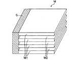
図1は、本発明の第1の実施の形態の光素子ODの構成を表す概念断面図である。光素子ODは、発光素子でも受光素子でも光変調素子でも良く、あるいはこれらを組み合わせたものであっても良い。この光素子ODは、基体B上に、分布ブラック反射鏡Mを有する。反射鏡Mは、特定の波長の入射光Lを反射する。反射する方向は、図示の如く反射鏡Mの主面に対して斜め方向でも良く、または主面に対して垂直方向でもよい。入射光Lの放出源は、図示の如く光素子ODの中に設けられていても良く、また外部に設けられていても良い。また、反射された入射光Lは、光素子ODの内部で変調あるいは光電変換などの処理を受けてもよく、または、そのまま外部に放出されてもよい。さらに、反射鏡Mに入射した入射光Lの一部は、反射されずに、反射鏡Mを透過するようにしてもよい。 FIG. 1 is a conceptual cross-sectional view showing the configuration of the optical element OD according to the first embodiment of the present invention. The optical element OD may be a light emitting element, a light receiving element, a light modulation element, or a combination thereof. This optical element OD has a distributed black reflecting mirror M on a base B. The reflecting mirror M reflects incident light L having a specific wavelength. The direction of reflection may be oblique with respect to the main surface of the reflecting mirror M, as shown, or may be perpendicular to the main surface. The emission source of the incident light L may be provided in the optical element OD as illustrated, or may be provided outside. The reflected incident light L may be subjected to processing such as modulation or photoelectric conversion inside the optical element OD, or may be emitted to the outside as it is. Further, a part of the incident light L incident on the reflecting mirror M may be transmitted through the reflecting mirror M without being reflected.
次に、図2〜図5を参照にして、反射鏡Mの構造について説明する。
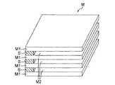
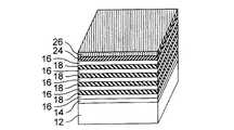
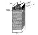
図2は、分布ブラック反射鏡Mの構造を示す概念斜視図である。反射鏡Mは、Al0.05Ga0.95Nからなる半導体層M1と、空気からなるギャップ層M2と、が交互に積層された構造である。言い換えると、反射鏡Mは、複数の半導体層M1が互いにほぼ等間隔に離間して積層された積層構造を有する。そして、それぞれの半導体層M1は、隣接する前記半導体層の間に介在して設けられた支持部Sによって支持されており、この支持部SはGaNからなる。反射鏡Mにおいて、波長λの入射光に対して高い反射率を得るためには、半導体層M1およびギャップ層M2の厚さを、それぞれλ/4n1およびλ/4n2とする。ここで、n1はAl0.05Ga0.95Nの屈折率約2.57、n2は空気の屈折率約1、である。例えば、400nmの入射光Lに対して高い反射率の反射鏡Mを得るためには、半導体層M1の厚さを約40nm、ギャップ層M2の厚さを約100nmにする。この反射鏡Mでは、半導体層M1のAl0.05Ga0.95Nと、ギャップ層M2の空気と、の大きな屈折率の差を利用して、入射光Lを高効率で反射する。Next, the structure of the reflecting mirror M will be described with reference to FIGS.
FIG. 2 is a conceptual perspective view showing the structure of the distributed black reflector M. As shown in FIG. The reflecting mirror M has a structure in which semiconductor layers M1 made of Al0.05 Ga0.95 N and gap layers M2 made of air are alternately stacked. In other words, the reflecting mirror M has a stacked structure in which a plurality of semiconductor layers M1 are stacked at substantially equal intervals. Each semiconductor layer M1 is supported by a support portion S provided between adjacent semiconductor layers, and the support portion S is made of GaN. In the reflecting mirror M, in order to obtain a high reflectance with respect to incident light having a wavelength λ, the thicknesses of the semiconductor layer M1 and the gap layer M2 are λ / 4n1 and λ / 4n2 , respectively. Here, n1 is a refractive index of Al0.05 Ga0.95 N of about 2.57, and n2 is a refractive index of air of about 1. For example, in order to obtain a reflecting mirror M having a high reflectivity with respect to incident light L of 400 nm, the thickness of the semiconductor layer M1 is set to about 40 nm and the thickness of the gap layer M2 is set to about 100 nm. In the reflecting mirror M, the incident light L is reflected with high efficiency by utilizing a large refractive index difference between Al0.05 Ga0.95 N of the semiconductor layer M1 and air of the gap layer M2.
ここで、図2の反射鏡Mでは、ギャップ層M2を空気からなる層にしたが、その他の気体あるいは真空空間からなる層とるすることもできる。また、図2の反射鏡では、半導体層M1をAl0.05Ga0.95Nからなる層にしたが、他の窒化物半導体からなる層にすることもできる。ただし、半導体層M1はAlを含有する窒化物半導体であることが望ましい。例えば、図2のようにAlGaNを用いると、AlGaNはGaNと比較して基礎吸収端の波長が大幅に短いので、反射鏡Mが反射する最短波長を大幅に短くすることができる。ただし、半導体層M1には、光素子ODの入射光Lのの波長に応じて、窒化物半導体以外のIII−V族半導体やSiを使用してもよい。また、各部の膜厚、層数、寸法などの関係は適宜変更することができる。Here, in the reflecting mirror M of FIG. 2, the gap layer M2 is a layer made of air, but it can also be a layer made of other gas or vacuum space. In the reflecting mirror of FIG. 2, the semiconductor layer M1 is a layer made of Al0.05 Ga0.95 N, but may be a layer made of another nitride semiconductor. However, the semiconductor layer M1 is preferably a nitride semiconductor containing Al. For example, when AlGaN is used as shown in FIG. 2, since the wavelength of the fundamental absorption edge of AlGaN is significantly shorter than that of GaN, the shortest wavelength reflected by the reflecting mirror M can be significantly shortened. However, for the semiconductor layer M1, a group III-V semiconductor other than a nitride semiconductor or Si may be used according to the wavelength of the incident light L of the optical element OD. In addition, the relationship among the film thickness, the number of layers, dimensions, and the like of each part can be changed as appropriate.
図3は、反射鏡Mの他の具体例を表す概念斜視図である。同図の例においては、反射鏡Mの一方のみに支持部Sが設けられ、いわば、半導体層M1は、「片持ち梁状」に支持されている。そして、層M1の間には、ギャップ層M2が形成されている。 FIG. 3 is a conceptual perspective view showing another specific example of the reflecting mirror M. FIG. In the example of the figure, the support portion S is provided only on one side of the reflecting mirror M, so to speak, the semiconductor layer M1 is supported in a “cantilever shape”. A gap layer M2 is formed between the layers M1.
図4及び図5は、反射鏡Mの他の具体例を表す概念斜視図である。これらの例においては、支持部Sが反射鏡Mのいずれかの側面において連続して設けられ、ここから半導体層M1のそれぞれが延在してDBRを形成している。換言すると、半導体層M1のそれぞれの端部が支持部Sに連結された構成を有する。図4及び図5の反射鏡Mでは、支持部Sにも半導体層M1と同様に、Al0.05Ga0.95Nを用いている。図4は、反射鏡Mの両端に支持部Sが設けられた例で、図5は、反射鏡Mの一端に支持部Sが設けられた例を、それぞれ表す。但し、本発明は、これらの具体例に限定されず、支持部Sは、反射鏡Mの周囲を取り囲むように設けられていても良く、または、反射鏡Mの内部の一部分を貫通するよう支柱状に設けられていても良い。4 and 5 are conceptual perspective views showing other specific examples of the reflecting mirror M. FIG. In these examples, the support portion S is continuously provided on either side of the reflecting mirror M, and each of the semiconductor layers M1 extends from here to form a DBR. In other words, each end portion of the semiconductor layer M1 is connected to the support portion S. 4 and 5, Al0.05 Ga0.95 N is used for the support portion S as well as the semiconductor layer M1. FIG. 4 shows an example in which the support portions S are provided at both ends of the reflecting mirror M, and FIG. 5 shows an example in which the support portions S are provided at one end of the reflecting mirror M, respectively. However, the present invention is not limited to these specific examples, and the support part S may be provided so as to surround the periphery of the reflecting mirror M, or the support pillar S may pass through a part of the inside of the reflecting mirror M. It may be provided in a shape.
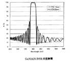
次に、図6〜図7を参照にして、反射鏡Mの特性について説明する。図6は、図2に示した反射鏡Mの反射率特性を表すグラフ図である。この図6は、図2の反射鏡Mの各層の膜厚を波長400nm前後の入射光Lに対して高い反射率が得られるように設計した場合のデータである。横軸は入射光Lの波長Wavelengthを、縦軸はこの入射光に対する反射率Rを、示している。この図6では、図2の反射鏡Mにおいて、Al0.05Ga0.95Nからなる半導体層M1と、空気からなるギャップ層M2と、を3ペア組み合わせた場合、及び4ペア組み合わせた場合の反射率Rを示している。Next, the characteristics of the reflecting mirror M will be described with reference to FIGS. FIG. 6 is a graph showing the reflectance characteristics of the reflecting mirror M shown in FIG. FIG. 6 shows data when the thickness of each layer of the reflecting mirror M in FIG. 2 is designed so as to obtain a high reflectance with respect to the incident light L having a wavelength of around 400 nm. The horizontal axis indicates the wavelength Wavelength of the incident light L, and the vertical axis indicates the reflectance R for the incident light. In FIG. 6, in the reflector M of FIG. 2, when the semiconductor layer M1 made of Al0.05 Ga0.95 N and the gap layer M2 made of air are combined in three pairs, and in the case where four pairs are combined The reflectance R is shown.
図6から分かるように、図2に示した反射鏡Mでは、3ペア積層しただけで、99%以上の高反射率が得られる。例えば、面発光レーザでは、閾電流密度を低減するために、DBRの反射率は高いほど好ましく、99%以上の高反射率の反射鏡が必要とされるが、図2の反射鏡Mでは、3ペア積層しただけで、このような高反射率が得られる。また、図2の反射鏡で、4ペア積層すれば99.9%以上の反射率が得られ、しかもその高反射帯域(ストップバンドの波長幅)は約60nmと非常に広くなる。また、反射率99.5%の高反射帯域は約140nmにもなる。このため、半導体層M1の厚さが設計値から5nm程度ずれても、400nmの波長の入射光Lに対して99.5%以上の反射率が得られる。このように、図2の反射鏡Mは、積層する層数が少なくても、高い特性を得ることができる。 As can be seen from FIG. 6, in the reflector M shown in FIG. 2, a high reflectance of 99% or more can be obtained only by stacking three pairs. For example, in the surface emitting laser, in order to reduce the threshold current density, the DBR reflectance is preferably as high as possible, and a reflector having a high reflectance of 99% or more is required. In the reflector M in FIG. Such a high reflectivity can be obtained only by stacking three pairs. Further, if four pairs of the reflecting mirrors in FIG. 2 are stacked, a reflectance of 99.9% or more can be obtained, and the high reflection band (wavelength width of the stop band) is as wide as about 60 nm. Further, the high reflection band having a reflectance of 99.5% is about 140 nm. For this reason, even if the thickness of the semiconductor layer M1 deviates by about 5 nm from the design value, a reflectance of 99.5% or more is obtained with respect to the incident light L having a wavelength of 400 nm. As described above, the reflecting mirror M in FIG. 2 can obtain high characteristics even if the number of layers to be stacked is small.
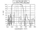
これに対し、比較例として、図7に、従来のDBRの反射率特性を示す。図7は、GaN層とAlN層とを交互に15ペアあるいは20ペア積層したDBRのデータである。図6と同様に、横軸は入射光Lの波長Wavelengthを、縦軸はこの入射光Lに対する反射率Rを、示している。この反射鏡も、波長が400nm前後において高い反射率が得られるように形成された反射鏡である。 In contrast, as a comparative example, FIG. 7 shows the reflectance characteristics of a conventional DBR. FIG. 7 shows DBR data in which 15 pairs or 20 pairs of GaN layers and AlN layers are alternately stacked. As in FIG. 6, the horizontal axis indicates the wavelength Wavelength of the incident light L, and the vertical axis indicates the reflectance R with respect to the incident light L. This reflecting mirror is also a reflecting mirror formed so as to obtain a high reflectance at a wavelength of around 400 nm.
図7から分かるように、GaN層とAlN層とを組み合わせた従来のDBRにおいては、15ペアの多層膜では99%の高反射率を得ることができない。99%の高反射率を得るためには、20ペア以上の多層膜を成長する必要がある。また、図7の従来のDBRにおいては、20ペアの多層膜を成長した場合でも、反射率99.5%以上の高反射帯域(ストップバンドの波長幅)は、約15nm程度と非常に狭い。このため、半導体層M1の厚さが設計値から1nm程度以上ずれると、400nmの波長の入射光Lに対して99.5%以上の反射率が得られなくなる。 As can be seen from FIG. 7, in a conventional DBR in which a GaN layer and an AlN layer are combined, a high reflectivity of 99% cannot be obtained with 15 pairs of multilayer films. In order to obtain a high reflectance of 99%, it is necessary to grow a multilayer film of 20 pairs or more. Further, in the conventional DBR of FIG. 7, even when 20 pairs of multilayer films are grown, the high reflection band (wavelength width of the stop band) having a reflectance of 99.5% or more is very narrow, about 15 nm. For this reason, if the thickness of the semiconductor layer M1 deviates from the design value by about 1 nm or more, a reflectance of 99.5% or more cannot be obtained with respect to the incident light L having a wavelength of 400 nm.
以上のように、図6に示す本実施形態のDBRは、図7に示す従来のDBRに比べ、少ない層数で高い特性が得られる。 As described above, the DBR of the present embodiment shown in FIG. 6 can obtain higher characteristics with a smaller number of layers than the conventional DBR shown in FIG.
もっとも、図2のようなギャップ層M2を用いた反射鏡Mを形成することは、従来、極めて困難であると考えられていた。なぜなら、従来のエッチング方法では、ギャップ層M2を図2のような形状にエッチングすることができなかったからである。即ち、前述のように、図2のギャップ層M2の厚さは100nm程度と薄く、図2のような形状にエッチングするには微細加工が要求される。しかし、窒化物半導体は結晶が硬いために、ドライ・エッチングを用いてこのような微細加工を行うことは困難である。また、ウェット・エッチングを用いた場合も、エッチング液が厚さ約100nmの間隙を浸入することが困難であるために、図2のような形状にエッチングすることは難しい。しかも、図2から分かるように、ギャップ層M2は、周期的に3〜4層形成する必要があり、高い加工精度が要求される。このため、従来の技術常識では、図2のようなギャップ層M2を形成することは極めて困難であると考えられていた。しかしながら本発明者は、ギャップ層M2を形成して高い反射率のDBRを得るべく各種の実験を繰り返した。その結果、独自に発明した気相エッチング法を用いて、これを実現できることを知得した。以下、図8〜図9を参照にして、この気相エッチング法を説明する。 However, it has been conventionally considered that it is extremely difficult to form the reflecting mirror M using the gap layer M2 as shown in FIG. This is because the conventional etching method could not etch the gap layer M2 into the shape shown in FIG. That is, as described above, the thickness of the gap layer M2 in FIG. 2 is as thin as about 100 nm, and fine processing is required for etching into the shape as shown in FIG. However, since a nitride semiconductor has a hard crystal, it is difficult to perform such fine processing using dry etching. Further, even when wet etching is used, it is difficult to etch into a shape as shown in FIG. 2 because it is difficult for the etchant to enter the gap having a thickness of about 100 nm. Moreover, as can be seen from FIG. 2, it is necessary to periodically form 3 to 4 gap layers M2, and high processing accuracy is required. For this reason, it has been considered that it is extremely difficult to form the gap layer M2 as shown in FIG. However, the present inventor repeated various experiments to form the gap layer M2 and obtain a DBR having a high reflectance. As a result, it was found that this can be realized by using the vapor-phase etching method originally invented. Hereinafter, the vapor phase etching method will be described with reference to FIGS.
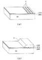
図8は、図2に示した反射鏡Mの製造方法を示す概念断面図である。 FIG. 8 is a conceptual cross-sectional view showing a manufacturing method of the reflecting mirror M shown in FIG.
まず、図8(a)に示すように、所定の基体Bの上に、MOCVD法(matal organic chemical vapor deposition:有機金属化学気相成長法)またはMBE法(molecular beam epitaxy:分子線エピタキシー)により、Al0.05Ga0.95Nからなる半導体層M1と、GaNからなるエッチング層Eと、の積層構造を形成する。First, as shown in FIG. 8 (a), an MOCVD method (matal organic chemical vapor deposition) or MBE method (molecular beam epitaxy) is performed on a predetermined substrate B. A stacked structure of a semiconductor layer M1 made of Al0.05 Ga0.95 N and an etching layer E made of GaN is formed.
次に、図8(b)に示すように、積層構造の一部を選択的に除去してその側面SFを露出させる。この除去は例えば、レジストなどのマスクとRIE(reactive ion etching:反応性イオンエッチング)あるいはイオン・ミリングなどのエッチング方法を用いて行うことができる。なお、図8(b)においては、積層構造のみを選択的にエッチングした例を表したが、基体Bまでエッチングしても良い。 Next, as shown in FIG. 8B, a part of the laminated structure is selectively removed to expose the side surface SF. This removal can be performed, for example, using a mask such as a resist and an etching method such as RIE (reactive ion etching) or ion milling. Although FIG. 8B shows an example in which only the laminated structure is selectively etched, etching up to the base B may be performed.
次に、図8(c)に示すように、本発明者が独自に発明した気相エッチング法を用いて、側面SFからエッチング層Eを選択的にエッチング除去する。即ち、
図8(b)の積層体を、水素を含有する雰囲気中で1000℃前後に昇温すると、エッチング層Eはエッチングされ、半導体層M1は殆どエッチングされない。これにより、エッチング層Eのみを選択的にエッチング除去することができる。Next, as shown in FIG. 8C, the etching layer E is selectively removed from the side surface SF by using the vapor phase etching method originally invented by the present inventors. That is,
When the stack of FIG. 8B is heated to about 1000 ° C. in an atmosphere containing hydrogen, the etching layer E is etched and the semiconductor layer M1 is hardly etched. Thereby, only the etching layer E can be selectively removed by etching.
次に、図8(d)に示すように、エッチングが所定量進行した段階でエッチングを停止する。その結果、エッチング層Eの一部が半導体層M1を支える支持部Sとして残留し、図2のDBR反射鏡Mが完成する。 Next, as shown in FIG. 8D, the etching is stopped when the etching proceeds by a predetermined amount. As a result, part of the etching layer E remains as the support portion S that supports the semiconductor layer M1, and the DBR reflector M of FIG. 2 is completed.
上記の気相エッチング法では、Alを含有しない窒化物半導体に比べて、Alを僅かでも含有した窒化物半導体のエッチング速度が大幅に低下することを利用している。即ち、図8(b)の積層体を水素を含有する雰囲気中で1000℃前後に昇温すると、GaNからなるエッチング層Eはエッチングされるのに対し、Al0.05Ga0.95Nからなる半導体層M1はほとんどエッチングされない。これは本発明者の独自の検討で得られた結果である。このようにGaNがエッチングされる理由について、本発明者は、GaNが高温で水素と反応し、Ga(気相)とNH3(気相)とに分解して昇華するからであると考えている。また、AlGaNがエッチングされないのは、Alを含有することにより、V属元素との結合力が強くなって分解が生じにくくなるからであると考えられる。そして、このエッチング速度の違いを利用して、選択的なエッチングを行うことができる。The above-described vapor phase etching method utilizes the fact that the etching rate of a nitride semiconductor containing even a small amount of Al is significantly lower than that of a nitride semiconductor containing no Al. That is, when the temperature of the laminated body of FIG. 8B is raised to about 1000 ° C. in an atmosphere containing hydrogen, the etching layer E made of GaN is etched, whereas from Al0.05 Ga0.95 N The resulting semiconductor layer M1 is hardly etched. This is a result obtained by the inventors' original study. The reason why GaN is etched in this way is that the present inventor thinks that GaN reacts with hydrogen at a high temperature and decomposes into Ga (gas phase) and NH3 (gas phase) and sublimates. Yes. Moreover, it is considered that AlGaN is not etched because, when Al is contained, the bonding force with the group V element becomes strong and decomposition does not easily occur. Then, selective etching can be performed by utilizing the difference in the etching rate.
ここで、図8では、半導体層M1がAlGaNからなり、エッチング層EがGaNからなる場合について説明したが、本発明は、これに限定されるものではない。即ち、半導体層M1のAl含有割合をエッチング層EのAl含有割合よりも高くすれば、エッチング層Eのエッチング速度が半導体層M1のエッチング速度よりも早くなるので、選択的なエッチングを行うことができる。例えば、半導体層M1をAlxGa1−xN(0<x≦1)とし、エッチング層EをAlyGa1−yN(0≦y<x)とすることができる。Here, although the case where the semiconductor layer M1 is made of AlGaN and the etching layer E is made of GaN has been described with reference to FIG. 8, the present invention is not limited to this. That is, if the Al content ratio of the semiconductor layer M1 is made higher than the Al content ratio of the etching layer E, the etching rate of the etching layer E becomes faster than the etching rate of the semiconductor layer M1, so that selective etching can be performed. it can. For example, the semiconductor layer M1 can be Alx Ga1-x N (0 <x ≦ 1), and the etching layer E can be Aly Ga1-y N (0 ≦ y <x).
また、本発明者の実験によれば、Inを含有する量が多い窒化物半導体はエッチング速度が早くなることも判明している。従って、例えば、半導体層M1をGaNやAlGaNとし、エッチング層EをInGaNとしても、選択的なエッチングを行うことができる。 In addition, according to experiments by the present inventors, it has been found that a nitride semiconductor having a large amount of In is increased in etching rate. Therefore, for example, even when the semiconductor layer M1 is GaN or AlGaN and the etching layer E is InGaN, selective etching can be performed.
また、本発明者の検討の結果、気相エッチングの雰囲気として、窒素、アンモニア、ヘリウム、アルゴン、キセノン及びネオンのうちのいずれかと水素との混合雰囲気、またはこれらのうちの2以上と水素との混合雰囲気、または水素雰囲気、を用いた場合に、良好なエッチングを行うことができた。 Further, as a result of the study by the present inventors, as an atmosphere for vapor phase etching, a mixed atmosphere of any one of nitrogen, ammonia, helium, argon, xenon, and neon and hydrogen, or two or more of these and hydrogen When a mixed atmosphere or a hydrogen atmosphere was used, good etching could be performed.
以上説明した気相エッチング法では、高いエッチング速度が得られる。例えば、本発明者の実験によれば、半導体層M1として厚さ40nmのAlGaN層を用い、エッチング層Eとして厚さ100nmのGaNを用いた場合に、水素と窒素を体積比で1:3の割合で混合した1気圧の雰囲気中で約1100℃に2分間保持したところ、エッチング層Eを、側面SFから約5μmの距離までサイドエッチングすることができた。このように高いエッチング速度が得られるので、図2のようなDBRを容易に形成することができる。 In the vapor phase etching method described above, a high etching rate can be obtained. For example, according to an experiment by the present inventor, when an AlGaN layer having a thickness of 40 nm is used as the semiconductor layer M1 and GaN having a thickness of 100 nm is used as the etching layer E, the volume ratio of hydrogen and nitrogen is 1: 3. When kept at about 1100 ° C. for 2 minutes in an atmosphere of 1 atmosphere mixed at a ratio, the etching layer E could be side-etched to a distance of about 5 μm from the side surface SF. Since such a high etching rate can be obtained, a DBR as shown in FIG. 2 can be easily formed.
これに対して、従来のウェット・エッチングを用いた場合には、エッチング液が厚さ100nmの間隙を浸入することが困難であるために、側面SFからサイドエッチングすることは極めて困難であった。また、AlGaNに対してGaNを優先的にエッチングするエッチング液もなかった。 On the other hand, when conventional wet etching is used, it is difficult to perform side etching from the side surface SF because it is difficult for the etching solution to enter the gap having a thickness of 100 nm. Also, there was no etchant that preferentially etches GaN over AlGaN.
また、気相エッチングは、上述のように、水素を含有する雰囲気で行うことができる。この雰囲気は、従来のCDEやRIEなどのドライエッチングにおいて用いられてきたいわゆるエッチングガスとは異なり、窒化物半導体に対して化学的な反応を顕著には生じない。また、気相エッチング法においては、従来用いられてきた腐食性の反応性ガスは用いない。このため、気相エッチングでは、腐食性のエッチング・ガスやプラズマなどによる結晶の損傷を生ずることなく、DBRを形成することができる。 Further, as described above, the vapor phase etching can be performed in an atmosphere containing hydrogen. Unlike the so-called etching gas that has been used in conventional dry etching such as CDE and RIE, this atmosphere does not cause a significant chemical reaction to the nitride semiconductor. In the vapor phase etching method, a corrosive reactive gas which has been conventionally used is not used. For this reason, in the vapor phase etching, the DBR can be formed without causing crystal damage due to corrosive etching gas or plasma.
次に、気相エッチング法を用いた、他のDBRの製造方法を説明する。図9は、図4または図5に示した反射鏡の製造方法を示す概念断面図である。図9については、図8に関して前述したものと同様の要素には同一の符号を付して、詳細な説明は省略する。 Next, another DBR manufacturing method using the vapor phase etching method will be described. FIG. 9 is a conceptual cross-sectional view showing a manufacturing method of the reflecting mirror shown in FIG. 4 or FIG. 9, the same elements as those described above with reference to FIG. 8 are denoted by the same reference numerals, and detailed description thereof is omitted.
図9に例示した製造方法においては、同図(b)の工程において、積層体の一部を選択的に除去し、この除去部分にAl0.05Ga0.95Nを形成することにより、支持部Sを形成する。このように支持部Sを埋め込み形成した後は、図8に関して前述したものと同様の工程により、エッチング層Eを気相エッチングする。但し、図9の反射鏡Mの場合には、支持部SがAl0.05Ga0.95Nなので、この支持部Sはエッチングされない。従って、この支持部Sによって気相エッチングを容易且つ確実に停止させることができる。その結果として、半導体層M1とギャップ層M2とにより形成される反射領域の寸法を厳密に制御することができる。In the manufacturing method illustrated in FIG. 9, in the step of FIG. 9B, by selectively removing a part of the stacked body and forming Al0.05 Ga0.95 N in the removed portion, The support part S is formed. After the support portion S is buried and formed in this manner, the etching layer E is vapor-phase etched by the same process as described above with reference to FIG. However, in the case of the reflecting mirror M of FIG. 9, since the support portion S is Al0.05 Ga0.95 N, the support portion S is not etched. Therefore, the gas phase etching can be easily and reliably stopped by the support portion S. As a result, it is possible to strictly control the size of the reflective region formed by the semiconductor layer M1 and the gap layer M2.
(第2の実施の形態)
第2の実施の形態の光素子の特徴の1つは、AlGaNと、有機材料と、を
交互に積層した分布ブラック反射鏡Mを備えている点である。光素子の全体の構成は第1の実施の形態(図1)と同様であり、詳細な説明は省略する。(Second Embodiment)
One of the features of the optical element of the second embodiment is that it includes a distributed black reflecting mirror M in which AlGaN and an organic material are alternately stacked. The overall configuration of the optical element is the same as that of the first embodiment (FIG. 1), and detailed description thereof is omitted.
図10は、第2の実施の形態の光素子の分布ブラック反射鏡Mの構造を示す概念断面図である。反射鏡Mは、AlGaNからなる半導体層M3と、透明な有機系高分子材料であるポリメタクリル酸メチル(PMMA)からなる有機膜M4と、が交互に7ペア積層された構造である。ここで、透明な有機系高分子材料としては、他に、ポリカーネート(PC)、ポリジエチレングリコールビスアリルカーボネート、ポリスチレン(PS)、硬質ポリ塩化ビニル(硬質PVC)、スチレン−メタクリル酸メチル共重合体(MS樹脂)、アクリロニトリル−スチレン共重合体(AS樹脂)、ポリメタクリル酸シクロヘキシル(PCHMA)、ポリ(4−メチルペンテン−1)(TPX)等を用いることもできる。また、後述の実施例で説明するように、有機膜M4に導電性を有する有機材料や、フォトクロミズムを示す有機材料を用いることもできる。図10の反射鏡Mにおいて、有機膜M4を構成する有機材料の屈折率は約1.3〜1.7であり、半導体層M3を構成するAlGaNの屈折率は約2.57である。図10の反射鏡Mでは、この有機材料と、AlGaNと、の大きな屈折率の差を利用して、入射光Lを高い効率で反射する。 FIG. 10 is a conceptual cross-sectional view illustrating the structure of the distributed black reflector M of the optical element according to the second embodiment. The reflecting mirror M has a structure in which 7 pairs of semiconductor layers M3 made of AlGaN and organic films M4 made of polymethyl methacrylate (PMMA), which is a transparent organic polymer material, are alternately stacked. Here, other transparent organic polymer materials include polycarbonate (PC), polydiethylene glycol bisallyl carbonate, polystyrene (PS), rigid polyvinyl chloride (rigid PVC), styrene-methyl methacrylate copolymer. (MS resin), acrylonitrile-styrene copolymer (AS resin), polycyclohexyl methacrylate (PCHMA), poly (4-methylpentene-1) (TPX), and the like can also be used. Further, as will be described in the examples described later, an organic material having conductivity or an organic material exhibiting photochromism can be used for the organic film M4. In the reflecting mirror M of FIG. 10, the refractive index of the organic material constituting the organic film M4 is about 1.3 to 1.7, and the refractive index of AlGaN constituting the semiconductor layer M3 is about 2.57. In the reflecting mirror M of FIG. 10, the incident light L is reflected with high efficiency by utilizing a large refractive index difference between the organic material and AlGaN.
図11は、図10に示した反射鏡Mの反射率特性を、従来の反射鏡と比較しながら示した図である。この図11は、反射鏡Mの各層の膜厚を波長400nm前後の入射光Lに対して高い反射率が得られるように設計した場合のデータである。また、従来例は、GaNとAlNとを20ペア組み合わせ、各層の膜厚を波長400nm前後の入射光Lに対して高い反射率が得られるように設計した場合のデータである。図11の横軸は入射光Lの波長Wavelengthを、縦軸はこの入射光Lに対する反射率Rを示している。 FIG. 11 is a diagram showing the reflectance characteristics of the reflecting mirror M shown in FIG. 10 in comparison with a conventional reflecting mirror. FIG. 11 shows data when the thickness of each layer of the reflecting mirror M is designed so as to obtain a high reflectance with respect to the incident light L having a wavelength of around 400 nm. The conventional example is data when 20 pairs of GaN and AlN are combined and the thickness of each layer is designed so as to obtain a high reflectance with respect to incident light L having a wavelength of around 400 nm. In FIG. 11, the horizontal axis indicates the wavelength Wavelength of the incident light L, and the vertical axis indicates the reflectance R with respect to the incident light L.
図11から分かるように、図10に示したAlGaN/PMMAの組み合わせによるDBRでは、7ペアで99.5%以上の高反射率を得ることができる。しかもその高反射帯域は約60nmと広く、さらに反射率99%以上の高反射帯域は約100nmにも及ぶ。これに対し、従来のAlN/GaN多層膜DBRでは、20ペア以上の多層膜を形成したDBRでも、反射率99.5%以上になる高反射帯域は約10nm程度と狭い。 As can be seen from FIG. 11, in the DBR by the combination of AlGaN / PMMA shown in FIG. 10, a high reflectance of 99.5% or more can be obtained with 7 pairs. Moreover, the high reflection band is as wide as about 60 nm, and the high reflection band with a reflectance of 99% or more extends to about 100 nm. On the other hand, in the conventional AlN / GaN multilayer DBR, even in a DBR in which a multilayer film of 20 pairs or more is formed, the high reflection band where the reflectivity is 99.5% or more is as narrow as about 10 nm.
図10に示したような有機膜M4を用いた反射鏡Mを形成することも、第1の実施の形態と同様に、従来は、極めて困難であると考えられていた。しかしながら、本発明者は、前述の気相エッチング法を用いて、このような反射鏡Mを形成できることを独自に知得した。この具体的な方法については、後述の実施例2で説明する。 Forming the reflecting mirror M using the organic film M4 as shown in FIG. 10 has been conventionally considered to be extremely difficult as in the first embodiment. However, the present inventor has uniquely known that such a reflecting mirror M can be formed using the above-described vapor phase etching method. This specific method will be described in Example 2 described later.
(実施例)
次に、上述した本発明の実施の形態の光素子について、実施例を参照しつつ、さらに詳細に説明する。以下、第1の実施例では第1の実施の形態の光素子のDBRを用いた窒化物半導体面発光レーザについて、第2の実施例では第2の実施の形態の光素子のDBRを用いた窒化物半導体面発光レーザについて、第3および第4の実施の形態ではその他の光素子について説明する。(Example)
Next, the optical element according to the embodiment of the present invention described above will be described in more detail with reference to examples. Hereinafter, in the first example, the nitride semiconductor surface emitting laser using the DBR of the optical element of the first embodiment is used, and in the second example, the DBR of the optical element of the second embodiment is used. As for the nitride semiconductor surface emitting laser, other optical elements will be described in the third and fourth embodiments.
(第1の実施例)
まず、本発明の第1の実施例として、第1の実施の形態の光素子のDBRを、窒化物半導体面発光レーザに適用した具体例について説明する。(First embodiment)
First, as a first example of the present invention, a specific example in which the DBR of the optical element of the first embodiment is applied to a nitride semiconductor surface emitting laser will be described.
図12は、第1の実施例の窒化物半導体面発光レーザの概念断面図である。図12は概念図であり、説明をしやすくするため、各層の倍率は変えて示している。サファイア基板12の上には、バッファ層14を介して、約100nmのGaN層18と、約40nmのAl0.05Ga0.95N層16と、を交互に4ペア積層した下側積層体MLが形成されている。この下側積層体MLの一部においてGaN層18が除去されてギャップ層20が形成され、AlGaN層(半導体層)16とギャップ層20との4ペアの積層による下側DBRが形成されている。この下側DBRの上には、SiドープのGaNからなりるn型コンタクト層24、MgドープのAl0.05Ga0.95Nからなる膜厚0.1μmのp型電流ブロック層26、が順次積層されている。このn型コンタクト層24、p型電流ブロック層26には開口が形成されている。そして、この開口はSiドープのAl0.05Ga0.95Nからなる第1のn型クラッド層28Aで埋め込まれている。この第1のn型クラッド層28Aと、p型電流ブロック層26と、の上には、SiドープのAl0.05Ga0.95Nからなる第2のn型クラッド層28B、InGaNを含むMQW構造の活性層30、MgドープのAl0.05Ga0.95Nからなるp型クラッド層32が順次形成されている。このp型クラッド層32の上には、約100nmのGaN層40と、約40nmのAl0.05Ga0.95N層42と、を交互に4ペア積層した上側積層体MLが形成されている。この上側積層体MLにおいても、GaN層40の一部が除去されてギャップ層44が形成され、Al0.05Ga0.95N層42とギャップ層44との4ペアの積層による上側DBRが形成されている。FIG. 12 is a conceptual cross-sectional view of the nitride semiconductor surface emitting laser according to the first embodiment. FIG. 12 is a conceptual diagram, and the magnification of each layer is changed for easy explanation. On the
図12の面発光レーザでは、n型コンタクト層24の露出部に設けられたn側電極50と、p型クラッド層32の露出部に設けられたp側電極60と、から活性層30に電流が注入される。ここで、p型電流ブロック層26は、活性層30に注入される電流を絞り込む働きをする。即ち、n側電極50からの電流は、p型電流ブロック層26を通らず、第1のn型クラッド層28Aを通り、この第1のn型クラッド層28Aの上方の活性層30に絞り込んで注入される。その結果、第1のクラッド層28Aの上方部分の活性層30から光が放射される。この光の波長は、活性層30の組成により調整することができ、図12のレーザでは約400nmになるようにした。放射された光は、活性層30の上下のDBRで増幅され、レーザ光となり、図中上下方向に放射される。ここで、前述のように、レーザ光を得るためにはDBRの反射率を99%以上にする必要がある。 In the surface emitting laser of FIG. 12, an electric current is supplied to the
以上説明した、図12の窒化物半導体面発光レーザでは、Al0.05Ga0.95N(n=2.57)層16、42と、空気(n=1)層20、44と、を用いることにより、屈折率の差が大きい材料を組み合わせたDBRを得ることができる。このため、図6に関して前述したように、わずか3ペア積層しただけでも、面発光レーザに必要な99%以上の反射率のDBRが得られる。そして、図10のように4ペア積層すれば99.9%の反射率が得られる。また、この図10のレーザでは、DBRを、低Al組成のAlGaNを用いて作ることができる。このように図10の窒化物半導体面発光レーザでは、少ない積層数で、かつ低Al組成の層により、高反射率のDBRを得ることができるので、製造が容易で、クラックが発生しにくく、歩留まりを高くすることができるる。In the nitride semiconductor surface emitting laser shown in FIG. 12 described above, the Al0.05 Ga0.95 N (n = 2.57) layers 16 and 42 and the air (n = 1) layers 20 and 44 are provided. By using it, a DBR combining materials having a large difference in refractive index can be obtained. Therefore, as described above with reference to FIG. 6, a DBR having a reflectivity of 99% or more necessary for a surface emitting laser can be obtained even when only three pairs are stacked. Then, if 4 pairs are stacked as shown in FIG. 10, a reflectance of 99.9% can be obtained. In the laser shown in FIG. 10, the DBR can be made using AlGaN having a low Al composition. As described above, in the nitride semiconductor surface emitting laser of FIG. 10, a high reflectivity DBR can be obtained with a small number of stacked layers and a layer having a low Al composition. Yield can be increased.
また、図12の窒化物半導体面発光レーザでは、図6に関して前述したように、99.9%以上の高反射帯域(ストップバンドの波長幅)が約60nmと非常に広く、また99.5%の高反射帯域が約140nmと非常に広いDBRを得ることができる。このため、DBRの各層の厚さ、共振器の厚さ、活性層の組成、等が設計値からある程度ずれてもレーザ光に大きな影響を与えず、安定したレーザ光を得ることができる。例えば、DBRの半導体層16、42の厚さが設計値から5nm程度ずれても、レーザー光に大きな影響を与えない。また、DBRのギャップ層20、44の厚さが設計値から15nm程度ずれても、レーザ光に大きな影響を与えない。 Further, in the nitride semiconductor surface emitting laser of FIG. 12, as described above with reference to FIG. 6, the high reflection band (the wavelength band of the stop band) of 99.9% or more is very wide as about 60 nm, and 99.5%. A DBR having a very wide reflection band of about 140 nm can be obtained. For this reason, even if the thickness of each DBR layer, the thickness of the resonator, the composition of the active layer, etc. deviate from the design value to some extent, the laser light is not greatly affected, and stable laser light can be obtained. For example, even if the thickness of the DBR semiconductor layers 16 and 42 deviates from the design value by about 5 nm, the laser light is not greatly affected. Further, even if the thickness of the DBR gap layers 20 and 44 is deviated by about 15 nm from the design value, the laser light is not greatly affected.
また、図12の窒化物半導体面発光レーザでは、99.9%以上の高い反射率のDBRが得られるので、発振閾電流密度を極めて小さくすることができる。 In addition, in the nitride semiconductor surface emitting laser of FIG. 12, a DBR having a high reflectance of 99.9% or more can be obtained, so that the oscillation threshold current density can be extremely reduced.
また、図12の窒化物半導体面発光レーザでは、DBRの積層数が少ないので、生産性も低くならない。 Further, in the nitride semiconductor surface emitting laser of FIG. 12, the productivity is not lowered because the number of DBR layers is small.
これに対し、従来、このような窒化物半導体面発光レーザのDBRとして、GaN層と、AlGaN層またはAlN層と、の組み合わせを用いることが考えられていた。このような従来のDBRを用いた場合には、図7に関して前述したように、99%以上の高反射率を得るために20ペア以上の多層膜を成長する必要がある。従って、図12の面発光レーザでは、活性層30の下側と上側のDBRで合わせて40ペア以上の多層膜を成長する必要がある。しかしながら、前述のように、このような40ペア以上の多層膜を成長させるとクラックが発生するのが避けられず、歩留まりが著しく低下してしまった。また、このDBRは、反射率99.5%以上の高反射帯域(ストップバンドの波長幅)が、約15nm程度と非常に狭く、DBRの各層の厚さ、共振器の厚さ、活性層の組成、等が設計値よりわずかにずれただけでも発振条件を満足できなくなるので、安定したレーザ光が得られなかった。 On the other hand, conventionally, it has been considered to use a combination of a GaN layer and an AlGaN layer or an AlN layer as the DBR of such a nitride semiconductor surface emitting laser. When such a conventional DBR is used, as described above with reference to FIG. 7, it is necessary to grow 20 pairs or more of multilayer films in order to obtain a high reflectance of 99% or more. Therefore, in the surface emitting laser of FIG. 12, it is necessary to grow a multilayer film of 40 pairs or more in total with the lower and upper DBRs of the
次に、図13〜図17を参照にして、本実施例の面発光レーザの製造方法について説明する。図13〜図17は、本実施例の面発光レーザの製造方法を概念的に示す斜視図である。図13〜図17では、サファイア基板12は実際は直径約5×104μmの円形であるが、この一部を切り取った状態を概念的に示している。また、図13〜図17では、説明をしやすくするため、各層の倍率を変えて示している。なお、図12の基板12は、図13の基板12を細かく切断したものであり、その一辺の長さは約5×102μmである。Next, a method for manufacturing the surface emitting laser according to the present embodiment will be described with reference to FIGS. 13 to 17 are perspective views conceptually showing the method for manufacturing the surface emitting laser according to the present embodiment. In FIGS. 13 to 17, the
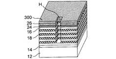
まず、図13に表したように、サファイア基板12の上にMOCVD法により、バッファ層14を10〜200nm程度の膜厚で成長する。そして、バッファ層14上に、膜厚約40nmのAl0.05Ga0.95N層16と、膜厚約100nmのGaN層18と、を交互に4ペア積層する。その後、SiドープのGaNからなるn型コンタクト層24を積層し、MgドープAl0.05Ga0.95Nからなるp型電流ブロック層26を0.1μmの厚みに積層する。First, as shown in FIG. 13, the
次に、ウェーハをMOCVD装置より取り出し、図14から分かるように、光露光プロセスによりレジストあるいはSiO2などからなるマスク300を形成する。そして、図14に示すように、反応性イオンエッチング(RIE)や反応性イオンビームエッチング(RIBE)等のドライエッチング法により、最下層のAl0.05Ga0.95N層16に達する矩形状の開口Hを形成する。その後、必要に応じてマスク300を除去した後、雰囲気の調整が可能な加熱炉へウェーハをセットする。そして、窒素ガスを4SLM流し、ウェーハ温度を1000℃まで約4分で昇温する。この過程においては、窒素雰囲気で加熱昇温することにより、ウェーハに付着していた水分や不純物ガスが除去される。なお、この昇温過程でのGaN層18の分解蒸発によるエッチングはほとんど無視できる。Next, the wafer is taken out from the MOCVD apparatus, and as can be seen from FIG. 14, a
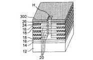
次に、図15から分かるように、ウェーハ温度が1000℃に達したところで、4SLMの窒素ガスに加えて、1SLMの水素ガスを導入し、SiドープGaN層18の気相エッチングを開始する。そして、この雰囲気において、1000℃で2分間保持した。この工程において、GaN層18は水素との反応により分解蒸発が促進され、気相エッチングが進行する。一方、Al0.05Ga0.95N層16のエッチングはほとんど進行せず、選択エッチングが行われる。すなわち、GaN層18およびGaNからなるn型コンタクト層24は、矩形状の穴Hの側面よりサイドエッチングされるが、Al0.05Ga0.95N層16のサイドエッチングは生じない。この選択エッチングにより、図15に示すように、矩形状の開口Hの側面より約20μmの範囲内のGaN層18は完全にエッチング除去され、その結果として、Al0.05Ga0.95N層16とギャップ層20とのDBR構造が形成された。その後、水素ガスの供給を停止して再び窒素雰囲気に戻し、室温まで降温した。なお、図15においては、GaN層18と共にGaNコンタクト層24も気相エッチングされる場合を例示した。これに対して、図12に例示したように、コンタクト層24の開口のサイズをDBRのギャップ層20のサイズよりも小さく形成したい場合には、GaNコンタクト層24にAlGaN層16よりも少量のAlを含有させれば良く、微量のAlを含有させれば足りる。このようにすれば、コンタクト層24の抵抗は上昇させることなく、気相エッチングの速度を大幅に低下させることが可能となる。その結果として、図10に表したように、コンタクト層24の開口のサイズをDBRのギャップ層20よりも小さく形成することも可能となる。Next, as can be seen from FIG. 15, when the wafer temperature reaches 1000 ° C., 1 SLM hydrogen gas is introduced in addition to 4 SLM nitrogen gas, and vapor phase etching of the Si-doped
次に、図16に示すように、電流狭窄用の窓Wを形成する。具体的には、ウェーハを加熱炉より取り出し、再び光露光プロセスによりp型電流ブロック層26上に図示しないマスクを形成し、ドライエッチング法あるいはKOHによるウエットエッチング法などにより幅約10μmの矩形状の窓Wを形成した。 Next, as shown in FIG. 16, a current confinement window W is formed. Specifically, the wafer is taken out from the heating furnace, a mask (not shown) is formed on the p-type
次に、図17に示すように、レーザ構造を積層形成する。具体的には、まず、窓Wを形成するために用いたレジストあるいはSiO2などのマスク(図示せず)を除去し、ウェーハを再びMOCVD装置へセットする。次に、アンモニアガスを供給し、窒素ガス20SLM、アンモニアガス10SLMの混合ガスを流し、基板温度を1080℃まで昇温する。次に、基板温度が1080℃に達すると同時に、トリメチルガリウム(TMG)、トリメチルアルミニウム(TMA)およびシランガスおよび水素ガスの供給を開始し、SiドープのAl0.05Ga0.95Nからなるn型クラッド層の28Bを成長する。この層の成長中に、p型電流ブロック層26に形成したストライプ状の窓Wは、埋め込まれて埋め込み部28Aが形成される。次に、InGaNを含むMQW構造の活性層30、MgドープのAl0.05Ga0.95Nからなるp型クラッド層32を積層する。その後、GaN層40と、Al0.05Ga0.95N層42と、を交互に4ペア積層する。この時、GaN層40とAl0.05Ga0.95N層42の膜厚は、下側DBRと同様にする。次に、MOCVD装置よりウェーハを取り出し、光露光プロセスによりマスクを形成し、ドライエッチング法により、p型クラッド層32に達する矩形上の穴Hを開口する。その後、上述した下側DBRの形成と同様の気相エッチング法により、Al0.05Ga0.95N層42とギャップ層44とのDBR構造を形成する。Next, as shown in FIG. 17, a laser structure is stacked. Specifically, first, the resist or the mask (not shown) such as SiO2 used for forming the window W is removed, and the wafer is set in the MOCVD apparatus again. Next, ammonia gas is supplied, a mixed gas of nitrogen gas 20SLM and ammonia gas 10SLM is flowed, and the substrate temperature is raised to 1080 ° C. Next, as soon as the substrate temperature reaches 1080 ° C., supply of trimethylgallium (TMG), trimethylaluminum (TMA), silane gas, and hydrogen gas is started, and n composed of Si-doped Al0.05 Ga0.95 N is started. 28B of the mold cladding layer is grown. During the growth of this layer, the stripe-shaped window W formed in the p-type
次に、光露光プロセスでマスクを形成し、ドライエッチング法によりp型クラッド層32およびn型コンタクト層26の一部をそれぞれを露出させ、素子分離を行う。そして、リフトオフ法により、n側電極50、p側電極60を形成して、図12に表した面発光レーザが完成する。 Next, a mask is formed by a light exposure process, the p-
以上説明した製造方法では、本発明者が独自に発明した気相エッチング法を用いることにより反射率が高いDBRを形成して、面発光の窒化物半導体レーザを得ることができる。これに対し、従来は、窒化物半導体をエッチングする有効な方法が存在せず、反射率の高いDBRを形成することが困難で、面発光の窒化物半導体レーザを得ることは困難であった。 In the manufacturing method described above, a surface-emitting nitride semiconductor laser can be obtained by forming a DBR having a high reflectivity by using a vapor phase etching method originally invented by the present inventor. On the other hand, conventionally, there is no effective method for etching a nitride semiconductor, it is difficult to form a highly reflective DBR, and it is difficult to obtain a surface emitting nitride semiconductor laser.
(第2の実施例)
次に、第2の実施例として、第2の実施の形態のDBRを、窒化物半導体面発光レーザに適用した具体例について説明する。(Second embodiment)
Next, as a second example, a specific example in which the DBR of the second embodiment is applied to a nitride semiconductor surface emitting laser will be described.
図18は、第2の実施例の窒化物半導体面発光レーザの概念断面図である。サファイア基板112の上には、バッファ層114を介して、GaNバッファ層115が形成されている。そしてGaNバッファ層115の上には、AlN層116とGaN層118とを交互に20ペア積層した下側DBR117が形成されている。この下側DBR117の上には、n型コンタクト層124、n型AlGaNクラッド層128、InGaNを含むMQW構造の活性層130、p型AlGaNクラッド層132、が順次形成されている。このp型AlGaNクラッド層132上には、n型AlGaN電流狭窄層134、第1のp型GaNコンタクト層136Aが形成され、これらの上には第2のp型GaNコンタクト層136Bが形成されている。この第2のp型GaNコンタクト層136Bの上には、MgドープのAl0.05Ga0.95Nからなる半導体層142と、ポリメタクリル酸メチル(PMMA)からなる有機膜層144と、を交互に7ペア積層した上側DBR141が形成されている。半導体層142および有機膜層144の膜厚は、それぞれ、λ/4n3およびλ/4n4である。ここで、n3はAl0.05Ga0.95Nの屈折率、n4はPMMAの屈折率、λは面発光レーザの発振波長である。FIG. 18 is a conceptual cross-sectional view of the nitride semiconductor surface emitting laser according to the second embodiment. A
図18の面発光レーザでは、n型コンタクト層124の露出部に設けられたn側電極150と、第1のp型クラッド層136Bおよび上側DBR141の露出部に設けられたp側電極160と、から活性層130に電流が注入される。ここで、n型電流ブロック層134は、活性層130に注入される電流を絞り込む働きをする。即ち、電流は第1のp型クラッド層136Aの下方の活性層130に絞り込んで注入される。その結果、第1のp型クラッド層136Aの下方部分の活性層130から光が放射される。放射された光は、活性層130の上側DBR141と下側DBR117で増幅され、レーザ光となり、図中上下方向に放射される。 In the surface emitting laser of FIG. 18, an n-
以上説明した、図18の窒化物半導体面発光レーザでは、上側DBR141に、Al0.05Ga0.95Nからなる半導体層142とPMMAからなる有機膜層144とを用いることにより、屈折率の差が大きい材料を組み合わせたDBRを得ることができる。このため、図11に関して前述したように、7ペアの積層で99.5%以上の反射率のDBRを得ることができる。また、図14の窒化物半導体面発光レーザでは、後述の製造方法からも分かるように、上側DBRを、低Al組成のAl0.05Ga0.95N層(半導体層)142を用いて作ることができる。このように図18の窒化物半導体面発光レーザでは、少ない積層数で、かつ低Al組成の層により、高反射率のDBRを得ることができるので、クラックが発生しにくくなり、歩留まりを高くすることができるる。In the nitride semiconductor surface emitting laser of FIG. 18 described above, the refractive index of the
ここで、図18の窒化物半導体面発光レーザでは、下側DBR121には、従来用いられていた、GaN層118とAlN層116の組み合わせのDBRを用いた。しかし上側DBR141に、半導体層142と有機膜層144の組み合わせのDBRを用いたので、クラックは発生しなかった。これに対し、上側DBR141にも従来のDBRを用いた場合には、クラックが発生し、歩留まりが著しく低下した。 Here, in the nitride semiconductor surface emitting laser of FIG. 18, a DBR that is a combination of the
また、図18の窒化物半導体面発光レーザでは、図11に関して前述したように、99.9%以上の高い反射率の上側DBRが得られるので、発振閾電流密度を小さくすることができる。 In the nitride semiconductor surface emitting laser shown in FIG. 18, the upper DBR having a high reflectivity of 99.9% or more can be obtained as described above with reference to FIG. 11, so that the oscillation threshold current density can be reduced.
以上説明した図18の窒化物半導体面発光レーザでは、下側DBRにGaN層118とAlN層116の組み合わせのDBRを用いた例を示したが、これを、上側DBRと同様に、半導体層と有機膜層の組み合わせのDBRにすることもできる。このようにすると、安定したレーザ光を得ることができる。即ち、半導体層と有機膜層の組み合わせのDBRでは、図11に関して前述したように、99.9%以上の高反射帯域(ストップバンドの波長幅)が約60nmと非常に広く、また99.5%の高反射帯域が約100nmにも及ぶ。このため、DBRの各層の厚さ、共振器の厚さ、活性層の組成、等が設計値からある程度ずれてもレーザ光の反射率が大きく影響されず、安定したレーザ光を得ることができる。例えば、DBRの半導体層の厚さが設計値から5nm程度ずれても、レーザー光に大きな影響を与えない。また、DBRの有機膜層の厚さが設計値から10nm程度ずれても、レーザ光に大きな影響を与えない。 In the nitride semiconductor surface emitting laser of FIG. 18 described above, an example in which a DBR of a combination of the
また、図18の窒化物半導体面発光レーザでは、PMMAからなる有機膜層144を用いたDBRを示したが、有機膜層144に、第2の実施の形態で説明した各種の透明な有機系高分子材料を用いることもできる。また、この有機膜層144に、導電性を有する有機材料を用いることもできる。このような導電性を有する有機材料には、π電子共役系高分子、直鎖状全π共役系高分子、非共役高分子がある。これらの有機材料は、それ自身あるいはドーピングにより金属領域の高い導電性を示す。さらに具体的には、π電子共役系高分子および直鎖状全π共役系高分子として、(1)脂肪族共役系:ポリアセチレン類、ポリジアセチレン類、(2)芳香族共役系:ポリ(p−フェニレン)類、(3)混合型共役系:ポリ(p−フェニレンビニレン)、ポリ(フェニレンカルコゲナイド)類、(4)複素環式共役系:ポリピロール、ポリチオフェン、ポリフラン、ポリカルバゾール、ポリキノリン類、(5)含ヘテロ原子共役系:ポリアニリン類、(6)複鎖型共役系(はしご型共役系)が挙げられる。また、非共役系高分子として、(1)側鎖にπ電子共役系基(カルバゾール、フェロセン、ピレン、ペリレン、フタロシアニン)を含む高分子、(2)大環状金属錯体(フタロシアニンなど)を主鎖に含む高分子:ニッケルフタロシアニン、(3)高分子ポリカチオン−TCNQラジカルアニオン塩、等が挙げられる。これらの、導電性を示す有機膜を用いると、上側DBR141を通して活性層130へ電流注入を行うことができ、p側電極160の形成を容易にすることができる。 In the nitride semiconductor surface emitting laser shown in FIG. 18, the DBR using the
次に、図19〜図25の概念斜視図を参照にして、図18の面発光レーザの製造方法について説明する。 Next, a method for manufacturing the surface emitting laser of FIG. 18 will be described with reference to the conceptual perspective views of FIGS.
まず、図19に示すように、サファイア基板112の上に、MOCVD法により、バッファ層114を10〜200nm程度の膜厚で成長する。そして、バッファ層114上に、GaNバッファ層115を0.3μmの膜厚で成長する。続いて、AlN層116と、GaN層118と、を交互に20ペア積層して、下側DBR117を形成する。その後、SiドープのGaNからなるn型コンタクト層124、SiドープのAl0.95Ga0.05Nからなるn型クラッド層128、InGaNを含むMQW構造の活性層130、MgドープのAl0.95Ga0.05Nからなるp型クラッド層132、SiドープのGaNからなる電流狭窄層134、を順次積層する。First, as shown in FIG. 19, the
次に、図20に示すように、ウェーハをMOCVD装置から取り出してエッチングマスクとなるSiO2を堆積し、光露光プロセスにより電流狭窄層134の一部を露出させて、SiO2に開口パターンHを形成する。Next, as shown in FIG. 20, the wafer is taken out from the MOCVD apparatus and SiO2 serving as an etching mask is deposited, and a part of the
次に、図21に示すように、電流狭窄層134に窓部CHを形成する。即ち、まず、図20のウェーハを加熱路にセットし、窒素ガスを4SLM流して、ウェーハを1000℃まで4分間で昇温する。この昇温過程では、GaNからなる電流狭窄層134の分解蒸発はほとんど無視できる。そして、ウェーハが1000℃に達したところで、水素ガスを導入し、窒素ガス4SLMと水素ガス1SLMの混合ガスを流した雰囲気において2分間保持した。その後、水素ガスの供給を停止して再び窒素雰囲気に戻し、室温まで降温した。この工程において、GaNからなる電流狭窄層134の、開口パターンHに露呈した部分は、水素との反応によって分解蒸発し、エッチングされる。一方、AlGaNからなるp型クラッド層132は、この条件ではエッチングされないため、このp型クラッド層132でエッチングは止まる。この工程により、GaNからなる電流狭窄層134に、p型クラッド層132に達する窓部CHが形成される。その後SiO2マスクを除去する。Next, as shown in FIG. 21, a window portion CH is formed in the
次に、図22に示すように、レーザ構造を積層形成する。即ち、図21の積層体を再びMOCVD装置にセットし、窒素ガス雰囲気で基板温度を1080℃まで昇温する。そして、基板温度が1080℃に達すると同時にアンモニアガスおよび水素ガスの供給を開始し、さらにGaとMgの原料ガスの供給を開始する。これにより、MgドープのGaNからなる第1のp型クラッド層136A(図18)、および第2のp型クラッド層136Bを形成する。次に、MgドープのAl0.05Ga0.95N層142と、MgドープのGaN層140と、を交互に7ペア積層し、Al0.05Ga0.95NとGaNの多層膜138を形成する。その後、MOCVD装置からウェーハを取り出す。Next, as shown in FIG. 22, a laser structure is stacked. That is, the laminate of FIG. 21 is set again in the MOCVD apparatus, and the substrate temperature is raised to 1080 ° C. in a nitrogen gas atmosphere. As soon as the substrate temperature reaches 1080 ° C., supply of ammonia gas and hydrogen gas is started, and supply of Ga and Mg source gases is started. Thus, a first p-
次に、図23から分かるように、光露光プロセスによりマスクを形成し、ドライエッチングにより多層膜138の一部をエッチングして、メサを形成する。この際、多層膜138の一番下側のAl0.05Ga0.95N層142はエッチングしない。その後、マスクを除去する。Next, as can be seen from FIG. 23, a mask is formed by an optical exposure process, and a part of the
次に、図24に示すように、上側DBR141を形成する。即ち、まず、前述の気相エッチング法を行うことにより、図24に点線で示した部分の下側のGaN層140を選択的にエッチングする。その後、溶媒に溶かしたPMMAを図23の積層体にスピンコートするか、あるいはPMMAを溶かした溶媒中にこの積層体をディップすることにより、上記の気相エッチングされた部分にPMMAからなる有機膜層144を形成する。この工程によって、Al0.95Ga0.05N層(半導体層)142と、有機膜層144と、を交互に7ペア積層したDBR141を形成する。Next, as shown in FIG. 24, the
次に、図25から分かるように、光露光プロセスでマスクを形成後、多層膜138の一番下側のAl0.95Ga0.05N層142をエッチングして、第2のp型コンタクト層136Bの一部を露出させる。その後、光露光プロセスおよびドライエッチングによりn型コンタクト層124の一部を露出させ、リフトオフによりp側電極160およびn側電極150(図18)を形成して、図18の面発光レーザが完成する。なお、図18は、図25の積層体を切断線CCに沿って切断した断面図である。ただし、図25ではn側電極150付近は示していない。Next, as can be seen from FIG. 25, after the mask is formed by the light exposure process, the lowermost Al0.95 Ga0.05 N layer 142 of the
以上説明した製造方法では、本発明者が独自に発明した気相エッチング法を用いることにより反射率が高いDBRを形成して、面発光の窒化物半導体レーザを得ることができる。これに対し、従来は、窒化物半導体をエッチングする有効な方法が存在せず、反射率の高いDBRを形成することが困難で、面発光の窒化物半導体レーザを得ることは困難であった。 In the manufacturing method described above, a surface-emitting nitride semiconductor laser can be obtained by forming a DBR having a high reflectivity by using a vapor phase etching method originally invented by the present inventor. On the other hand, conventionally, there is no effective method for etching a nitride semiconductor, it is difficult to form a highly reflective DBR, and it is difficult to obtain a surface emitting nitride semiconductor laser.
(第3の実施例)
次に、本発明の第3の実施例として、第1の実施の形態のDBRと、端面出射型のInGaAsP系半導体レーザと、を組み合わせた光素子について説明する。(Third embodiment)
Next, as a third example of the present invention, an optical element in which the DBR according to the first embodiment and an edge-emitting InGaAsP semiconductor laser are combined will be described.
図26は、第3の実施例の光素子の概念断面図である。基板SUの上には、発振波長1.55μmの端面出射型のInGaAsP系半導体レーザLDがマウントされている。基板SUの表面には、窒化物半導体レーザLDの前面に斜面Pが形成され、この斜面Pの上に反射鏡Mが設けられている。この反射鏡Mは、Al0.05Ga0.95Nからなる半導体層M1と、空気からなるギャップ層M2と、を交互に3ペア積層した構造である。そして、レーザ素子LBから放出されたレーザ光Lは、反射鏡Mにより反射されて基板SUに対して略垂直上方に出射される。基板SUには、主面が(100)面から所定の傾斜方位を有するシリコンウェーハを用いた。そして、斜面Pは、このシリコンウェーハの(111)面により形成した。FIG. 26 is a conceptual cross-sectional view of the optical element of the third embodiment. On the substrate SU, an end face emission type InGaAsP semiconductor laser LD having an oscillation wavelength of 1.55 μm is mounted. On the surface of the substrate SU, a slope P is formed in front of the nitride semiconductor laser LD, and a reflecting mirror M is provided on the slope P. The reflecting mirror M has a structure in which three pairs of semiconductor layers M1 made of Al0.05 Ga0.95 N and gap layers M2 made of air are alternately stacked. Then, the laser light L emitted from the laser element LB is reflected by the reflecting mirror M and is emitted substantially vertically upward with respect to the substrate SU. As the substrate SU, a silicon wafer having a principal surface with a predetermined tilt orientation from the (100) plane was used. The slope P was formed by the (111) plane of this silicon wafer.
図26の反射鏡Mの基本構造は図2に関して前述したものと同様であるが、
波長1.55μmの光に対する反射率が高くなるように、半導体層M1の膜厚を約150nm、ギャップ層M2の膜厚を約390nmとした。この反射鏡Mの反射率特性を、図27に示す。図27に示したように、この反射鏡Mは、波長1.55nmを中心として非常に広い波長範囲において高い反射率が得られる。The basic structure of the reflector M in FIG. 26 is the same as that described above with reference to FIG.
The thickness of the semiconductor layer M1 was set to about 150 nm and the thickness of the gap layer M2 was set to about 390 nm so that the reflectance with respect to light having a wavelength of 1.55 μm was increased. The reflectance characteristics of the reflecting mirror M are shown in FIG. As shown in FIG. 27, the reflecting mirror M can obtain a high reflectance in a very wide wavelength range centering on a wavelength of 1.55 nm.
以上説明した図26の光素子では、Al0.05Ga0.95Nからなる半導体層M1と、空気からなるギャップ層M2と、からなる反射鏡Mを用いたので、発振波長1.55μmのレーザ光を極めて高い反射率で反射することができる。このため、基板SUに対して垂直方向に波長1.55μmのレーザ光を出射する光素子において、発光効率を極めて高くすることができる。In the optical element of FIG. 26 described above, since the reflecting mirror M including the semiconductor layer M1 made of Al0.05 Ga0.95 N and the gap layer M2 made of air is used, the oscillation wavelength is 1.55 μm. Laser light can be reflected with a very high reflectance. For this reason, in the optical element that emits laser light having a wavelength of 1.55 μm in the direction perpendicular to the substrate SU, the light emission efficiency can be extremely increased.
また、図26の光素子の反射鏡Mは、図27に示したように、反射する光の波長範囲が非常に広い。従って、レーザLDのマウント位置、反射鏡Mの各層の膜厚、レーザ光Lの波長、等が多少ずれても反射率がほとんど変化しない。このため、図26の光素子では、安定した動作が得られる。 26 has a very wide wavelength range of reflected light, as shown in FIG. Therefore, the reflectance hardly changes even if the mounting position of the laser LD, the film thickness of each layer of the reflecting mirror M, the wavelength of the laser light L, etc. are slightly shifted. Therefore, a stable operation can be obtained with the optical element of FIG.
また、図26の光素子の反射鏡Mは、図2に関して前述したように、少ない積層数で高い反射率が得られる。このため、図26の光素子を用いることで、製造を容易にし、歩留まりを高くすることがきる。 In addition, as described above with reference to FIG. 2, the reflector M of the optical element in FIG. 26 can obtain a high reflectance with a small number of layers. For this reason, by using the optical element of FIG. 26, the manufacturing can be facilitated and the yield can be increased.
以上説明した、図26の光素子の反射鏡Mは、半導体層M1、ギャプ層M2の膜厚を必要に応じて調整することで、反射するレーザー光Lの波長を変えることができる。これにより、図26のInGaAsP系半導体レーザLDの替わりに、InGaAs系レーザ、InGaAlP系レーザ、GaInNAs系レーザを用いることもできる。 26 described above can change the wavelength of the reflected laser beam L by adjusting the film thicknesses of the semiconductor layer M1 and the gap layer M2 as necessary. As a result, an InGaAs laser, InGaAlP laser, or GaInNAs laser can be used instead of the InGaAsP semiconductor laser LD of FIG.
また、図26光素子の反射鏡Mは、半導体層M1、ギャプ層M2の膜厚を必要に応じて調整することで、異なる波長のレーザ光Lに対する共通の反射鏡として用いることが可能である。即ち、この反射鏡は図27及び図11から分かるように、高反射率で、かつ、光反射率領域が広いので、波長の異なる数種類のレーザ光Lに対する共通の反射鏡として用いることができる。例えば、この反射鏡を、光ディスクの信号読み取り・書き込み用の光ピックアップの一部に用いることができる。この光ピックアップでは、DVD用のレーザと、CD用のレーザと、を併用する場合が多いが、この反射鏡を用いることで、両方のレーザ光に対して高い反射率を得ることが出来る。 26 can be used as a common reflecting mirror for laser light L having different wavelengths by adjusting the film thicknesses of the semiconductor layer M1 and the gap layer M2 as necessary. . That is, as can be seen from FIG. 27 and FIG. 11, this reflecting mirror has a high reflectivity and a wide light reflectivity region, so that it can be used as a common reflecting mirror for several types of laser beams L having different wavelengths. For example, the reflecting mirror can be used as a part of an optical pickup for reading and writing signals on an optical disk. In this optical pickup, a DVD laser and a CD laser are often used in combination, but by using this reflecting mirror, a high reflectance can be obtained for both laser beams.
(第4の実施例)
次に、本発明の第4の実施例として、第2の実施の形態のDBRと、端面出射型の窒化物系半導体レーザと、を組み合わせた光素子について説明する。(Fourth embodiment)
Next, as a fourth example of the present invention, an optical element in which the DBR of the second embodiment and an edge-emitting nitride semiconductor laser are combined will be described.
図28は、第4の実施例の光素子の概念斜視図である。サファイア基板SUの上には、端面放出型の窒化物半導体レーザLDがマウントされている。サファイア基板SUの表面には、レーザ固定層230を介して窒化物半導体レーザLDがマウントされている。そして、この窒化物半導体レーザLDの前面に斜面Pが形成され、この斜面Pの上に反射鏡Mが設けられている。この反射鏡Mの構造は、図6に関して前述したものと同様である。そして、窒化物半導体レーザLDから放出されたレーザ光Lは、反射鏡Mにより反射されて基板SUに対して略垂直上方に出射される。 FIG. 28 is a conceptual perspective view of an optical element according to the fourth embodiment. On the sapphire substrate SU, an edge-emitting nitride semiconductor laser LD is mounted. A nitride semiconductor laser LD is mounted on the surface of the sapphire substrate SU via a
図28の光素子では、半導体層M3と有機膜層M4とからなる反射鏡Mを用いたので、端面出射型の窒化物半導体レーザLDからのレーザ光を極めて高い反射率で反射することができる。このため、基板SUに対して垂直方向にレーザ光を出射する光素子において、発光効率を高くすることができる。 In the optical element of FIG. 28, since the reflecting mirror M composed of the semiconductor layer M3 and the organic film layer M4 is used, the laser light from the edge emitting nitride semiconductor laser LD can be reflected with an extremely high reflectance. . For this reason, in the optical element which emits a laser beam in the direction perpendicular to the substrate SU, the light emission efficiency can be increased.
また、図28の光素子の反射鏡Mは、図11に示したように、反射する光の波長範囲が非常に広い。従って、レーザLDのマウント位置、反射鏡Mの各層の膜厚、レーザ光Lの波長、等が多少ずれても反射率がほとんど変化しない。このため、図28の光素子では、安定した動作が得られる。 Further, as shown in FIG. 11, the reflecting mirror M of the optical element in FIG. 28 has a very wide wavelength range of reflected light. Therefore, the reflectance hardly changes even if the mounting position of the laser LD, the film thickness of each layer of the reflecting mirror M, the wavelength of the laser light L, etc. are slightly shifted. Therefore, a stable operation can be obtained with the optical element of FIG.
また、図28の光素子の反射鏡Mは、図11に関して前述したように、少ない積層数で高い反射率が得られる。このため、図28の光素子を用いることで、製造を容易にし、歩留まりを高くすることがきる。 Further, as described above with reference to FIG. 11, the reflector M of the optical element of FIG. 28 can obtain a high reflectance with a small number of layers. For this reason, by using the optical element of FIG. 28, the manufacturing can be facilitated and the yield can be increased.
次に、この製造方法について、図29(a)〜(b)を参照にして説明する。 Next, this manufacturing method will be described with reference to FIGS.
まず、図29(a)から分かるように、サファイア(0001)基板SU上に、低温バッファ層を介して、約2μmの厚さの第1のGaN層200を形成し、その上にSiO2パターン210を形成する。その後、図19Aに示すように、SiO2パターン210の<11−20>方向に、ストライプ状の窓を持つパターンTを形成する。なお、ここで、(0001)面を主面とするGaN基板を用いることもできる。First, as can be seen from FIG. 29A, a
次に、図29(b)に示すように、上記のSiO2パターン210の窓Tを利用して、MOCVD法によりGaNを選択成長させることにより、{1−101}ファセット面Pを有する第2のGaN層220を形成する。Next, as shown in FIG. 29 (b), by using the window T of the SiO2 pattern 210 described above, GaN is selectively grown by the MOCVD method, so that the second surface having the {1-101} facet plane P is obtained. The
次に、露呈されたSiO2パターン220を除去した後、ファセット面P上に、AlGaN層M3と、GaN層(図示しない)と、の多層膜を形成する。そして、第2の実施例で説明した方法によりGaN層を選択的にエッチングして、有機膜層M4を形成する。その後、レーザ固定層230を介してレーザLDをマウントし、図28の光素子が得られる。Next, after removing the exposed SiO2 pattern 220, a multilayer film of an
以上説明した図28の光素子では、DBRの有機膜M4の材料としてフォトクロミズムを示す材料を使っても良い。その材料としては、(1)スペロベンゾピラン系高分子、(2)フルギト系分子、(3)ジアリールエテン系分子、(4)シクロファン系分子、等を用いることができる。一般に、フォトクロミズムを示す材料は、光励起状態において化学結合を組み替える性質を持つため、光を受けると、電子状態の異なる別の異性体へ変換する。このため、吸収スペクトルの異なる二つの異性体を可逆的に生成することができる。これにより、光スイッチ機能を持つ高反射率のDBRを形成することができる。 In the optical element of FIG. 28 described above, a material exhibiting photochromism may be used as the material of the DBR organic film M4. As the material, (1) a spirobenzopyran polymer, (2) a fulgite molecule, (3) a diarylethene molecule, (4) a cyclophane molecule, or the like can be used. In general, a material exhibiting photochromism has a property of recombining chemical bonds in a photoexcited state, so that when receiving light, it is converted into another isomer having a different electronic state. For this reason, two isomers having different absorption spectra can be reversibly generated. Thereby, a highly reflective DBR having an optical switch function can be formed.
以上、具体例を参照しつつ、本発明の実施の形態について説明した。しかし本発明は、これらの具体例に限定されるものではない。 The embodiments of the present invention have been described above with reference to specific examples. However, the present invention is not limited to these specific examples.
例えば、本実施形態の反射鏡を、LED(light emitting diode:発光ダイオード)の裏面側における反射ミラーとして使用できる。 For example, the reflecting mirror of this embodiment can be used as a reflecting mirror on the back side of an LED (light emitting diode).
また、AlxGa1−xN(0≦X≦1)層とギャップ層との多層構造、またはAlxGa1−xN(0≦X≦1)層と有機膜層との多層構造、により形成された反射鏡を、異種材料同士の接着技術により、InGaAs系レーザ、InGaAsP系レーザ、InGaAlP系レーザ、GaAlNAs系レーザなどの上下に接着することもできる。これにより、例えば従来良好なDBR材料のなかったInGaAsP系などにおいても面発光レーザが実現可能である。A multilayer structure of an Alx Ga1-x N (0 ≦ X ≦ 1) layer and a gap layer, or a multilayer structure of an Alx Ga1-x N (0 ≦ X ≦ 1) layer and an organic film layer; The reflecting mirror formed by the above can be bonded to the top and bottom of an InGaAs laser, an InGaAsP laser, an InGaAlP laser, a GaAlNAs laser, or the like by a bonding technique between different materials. Thereby, for example, a surface emitting laser can be realized even in an InGaAsP system which has not had a good DBR material.
OD 光素子
M 分布ブラック反射鏡
M1 半導体層
M2 ギャップ層
S 支持部
E エッチング層
M3 半導体層
M4 有機膜層
ML 反射鏡
16 Al0.05Ga0.95Nからなる半導体層
20 空気からなるギャップ層
30 活性層
42 Al0.05Ga0.95Nからなる半導体層
44 空気からなるギャップ層
117 下側DBR
130 活性層
141 上側DBR
142 Al0.05Ga0.95Nからなる半導体層
144 ポリメタクリル酸メチル(PMMA)からなる有機膜層OD optical element M distributed black reflector M1 semiconductor layer M2 gap layer S support part E etching layer M3 semiconductor layer M4 organic film
130
142
Claims (12)
Translated fromJapanese前記反射鏡は、アルミニウムを含有する窒化物半導体からなるほぼ同一の膜厚の複数の半導体層と、有機膜からなるほぼ同一の膜厚の複数の有機膜層と、が交互に積層された積層体であることを特徴とする光素子。An optical element having a reflecting mirror for reflecting light,
The reflecting mirror is a laminate in which a plurality of semiconductor layers having substantially the same thickness made of a nitride semiconductor containing aluminum and a plurality of organic film layers having substantially the same thickness made of an organic film are alternately stacked. An optical element characterized by being a body.
前記反射鏡を、
アルミニウムを含有する第1の窒化物半導体からなる半導体層と、前記第1の窒化物半導体よりもアルミニウムの含有割合が小さい第2の窒化物半導体からなるエッチング層と、を交互に積層した積層体を形成する工程と、
前記積層体を水素を含有する雰囲気中で加熱することにより、前記積層体の端面に露出した前記エッチング層をエッチングして隣接する前記半導体層の間に間隙を形成する工程と、
前記間隙に有機膜層を形成する工程と、により形成することを特徴とする光素子の製造方法。A method of manufacturing an optical element including a reflecting mirror that reflects light,
The reflector,
A laminate in which a semiconductor layer made of a first nitride semiconductor containing aluminum and an etching layer made of a second nitride semiconductor having a smaller aluminum content than the first nitride semiconductor are alternately laminated. Forming a step;
Heating the stacked body in an atmosphere containing hydrogen to etch the etching layer exposed on the end face of the stacked body to form a gap between the adjacent semiconductor layers;
Forming an organic film layer in the gap, and forming the optical element.
Priority Applications (1)
| Application Number | Priority Date | Filing Date | Title |
|---|---|---|---|
| JP2005330273AJP3840253B2 (en) | 2000-09-22 | 2005-11-15 | Optical element and manufacturing method thereof |
Applications Claiming Priority (2)
| Application Number | Priority Date | Filing Date | Title |
|---|---|---|---|
| JP2000289396 | 2000-09-22 | ||
| JP2005330273AJP3840253B2 (en) | 2000-09-22 | 2005-11-15 | Optical element and manufacturing method thereof |
Related Parent Applications (1)
| Application Number | Title | Priority Date | Filing Date |
|---|---|---|---|
| JP2001269231ADivisionJP2002176226A (en) | 2000-09-22 | 2001-09-05 | Optical element and manufacturing method thereof |
Publications (2)
| Publication Number | Publication Date |
|---|---|
| JP2006074070A JP2006074070A (en) | 2006-03-16 |
| JP3840253B2true JP3840253B2 (en) | 2006-11-01 |
Family
ID=36154270
Family Applications (1)
| Application Number | Title | Priority Date | Filing Date |
|---|---|---|---|
| JP2005330273AExpired - Fee RelatedJP3840253B2 (en) | 2000-09-22 | 2005-11-15 | Optical element and manufacturing method thereof |
Country Status (1)
| Country | Link |
|---|---|
| JP (1) | JP3840253B2 (en) |
Families Citing this family (2)
| Publication number | Priority date | Publication date | Assignee | Title |
|---|---|---|---|---|
| US8525221B2 (en) | 2009-11-25 | 2013-09-03 | Toshiba Techno Center, Inc. | LED with improved injection efficiency |
| CN111817682A (en)* | 2020-07-27 | 2020-10-23 | 松山湖材料实验室 | A thin-film bulk acoustic wave resonator and its preparation method |
- 2005
- 2005-11-15JPJP2005330273Apatent/JP3840253B2/ennot_activeExpired - Fee Related
Also Published As
| Publication number | Publication date |
|---|---|
| JP2006074070A (en) | 2006-03-16 |
Similar Documents
| Publication | Publication Date | Title |
|---|---|---|
| US7306961B2 (en) | Optical device, surface emitting type device and method for manufacturing the same | |
| US6121634A (en) | Nitride semiconductor light emitting device and its manufacturing method | |
| Choquette et al. | Vertical-cavity surface emitting lasers: moving from research to manufacturing | |
| US7026182B2 (en) | Semiconductor device, semiconductor laser, their manufacturing methods and etching methods | |
| US6689631B2 (en) | Semiconductor light-emitting device with improved electro-optical characteristics and method of manufacturing the same | |
| EP1746694B1 (en) | Vcsel system with transverse p/n junction | |
| US20030168653A1 (en) | Semiconductor light-emitting device, method for fabricating the same and optical disk apparatus | |
| JP2000261106A (en) | Semiconductor light emitting device, method of manufacturing the same, and optical disk device | |
| US20020173089A1 (en) | Vertical cavity surface emitting laser with buried dielectric distributed bragg reflector | |
| KR100440187B1 (en) | An optical device, a surface light emitting device, and a manufacturing method of them | |
| JP3840253B2 (en) | Optical element and manufacturing method thereof | |
| JP2003031894A (en) | Semiconductor laser and its manufacturing method | |
| JPH0629612A (en) | Manufacture of surface emission-type semiconductor laser and laser obtained by above manufacture | |
| US20090155942A1 (en) | Hybrid metal bonded vertical cavity surface emitting laser and fabricating method thereof | |
| US20050118741A1 (en) | Method for fabricating semiconductor optical device | |
| JP4876428B2 (en) | Semiconductor light emitting device | |
| JP2007013207A (en) | Semiconductor light emitting device | |
| US5309472A (en) | Semiconductor device and a method for producing the same | |
| JPH04316387A (en) | Surface light emitting laser | |
| JPH10313148A (en) | Method for manufacturing semiconductor laser device | |
| JPH06204599A (en) | Semiconductor laser and manufacture thereof | |
| JP2002261398A (en) | Optical communication system | |
| JP2003037338A (en) | Semiconductor light emitting device, method of manufacturing the same, and optical disk device | |
| JPH10154850A (en) | Vertical cavity semiconductor light emitting device, light emitting device, optical disk device, recording device, and etching method | |
| JP2002252428A (en) | Optical communication system using long wavelength surface emitting laser device |
Legal Events
| Date | Code | Title | Description |
|---|---|---|---|
| TRDD | Decision of grant or rejection written | ||
| A01 | Written decision to grant a patent or to grant a registration (utility model) | Free format text:JAPANESE INTERMEDIATE CODE: A01 Effective date:20060721 | |
| A61 | First payment of annual fees (during grant procedure) | Free format text:JAPANESE INTERMEDIATE CODE: A61 Effective date:20060804 | |
| FPAY | Renewal fee payment (event date is renewal date of database) | Free format text:PAYMENT UNTIL: 20090811 Year of fee payment:3 | |
| FPAY | Renewal fee payment (event date is renewal date of database) | Free format text:PAYMENT UNTIL: 20100811 Year of fee payment:4 | |
| FPAY | Renewal fee payment (event date is renewal date of database) | Free format text:PAYMENT UNTIL: 20100811 Year of fee payment:4 | |
| FPAY | Renewal fee payment (event date is renewal date of database) | Free format text:PAYMENT UNTIL: 20110811 Year of fee payment:5 | |
| FPAY | Renewal fee payment (event date is renewal date of database) | Free format text:PAYMENT UNTIL: 20110811 Year of fee payment:5 | |
| FPAY | Renewal fee payment (event date is renewal date of database) | Free format text:PAYMENT UNTIL: 20120811 Year of fee payment:6 | |
| FPAY | Renewal fee payment (event date is renewal date of database) | Free format text:PAYMENT UNTIL: 20120811 Year of fee payment:6 | |
| FPAY | Renewal fee payment (event date is renewal date of database) | Free format text:PAYMENT UNTIL: 20130811 Year of fee payment:7 | |
| LAPS | Cancellation because of no payment of annual fees |