JP3840205B2 - Ultrasonic probe and manufacturing method thereof - Google Patents
Ultrasonic probe and manufacturing method thereofDownload PDFInfo
- Publication number
- JP3840205B2 JP3840205B2JP2003169659AJP2003169659AJP3840205B2JP 3840205 B2JP3840205 B2JP 3840205B2JP 2003169659 AJP2003169659 AJP 2003169659AJP 2003169659 AJP2003169659 AJP 2003169659AJP 3840205 B2JP3840205 B2JP 3840205B2
- Authority
- JP
- Japan
- Prior art keywords
- vertical
- electrode layer
- ultrasonic probe
- grooves
- vertical electrode
- Prior art date
- Legal status (The legal status is an assumption and is not a legal conclusion. Google has not performed a legal analysis and makes no representation as to the accuracy of the status listed.)
- Expired - Fee Related
Links
- 239000000523sampleSubstances0.000titleclaimsdescription76
- 238000004519manufacturing processMethods0.000titleclaimsdescription45
- 238000000926separation methodMethods0.000claimsdescription79
- 239000011347resinSubstances0.000claimsdescription66
- 229920005989resinPolymers0.000claimsdescription66
- 239000000463materialSubstances0.000claimsdescription44
- 239000002131composite materialSubstances0.000claimsdescription37
- 238000000034methodMethods0.000claimsdescription34
- 239000011810insulating materialSubstances0.000claimsdescription23
- 238000013329compoundingMethods0.000claimsdescription18
- 230000003014reinforcing effectEffects0.000claimsdescription16
- 230000008569processEffects0.000claimsdescription11
- 239000012779reinforcing materialSubstances0.000claimsdescription6
- 238000005304joiningMethods0.000claimsdescription4
- 238000005520cutting processMethods0.000description28
- 230000015572biosynthetic processEffects0.000description12
- 238000009413insulationMethods0.000description9
- 239000000805composite resinSubstances0.000description5
- 230000008901benefitEffects0.000description4
- 230000035945sensitivityEffects0.000description4
- 239000000853adhesiveSubstances0.000description3
- 230000001070adhesive effectEffects0.000description3
- 238000010586diagramMethods0.000description3
- 230000005684electric fieldEffects0.000description3
- 238000002955isolationMethods0.000description3
- 239000002861polymer materialSubstances0.000description3
- 238000010276constructionMethods0.000description2
- 239000011162core materialSubstances0.000description2
- 230000007423decreaseEffects0.000description2
- 238000003745diagnosisMethods0.000description2
- 230000000694effectsEffects0.000description2
- 239000003822epoxy resinSubstances0.000description2
- 230000010287polarizationEffects0.000description2
- 229920000647polyepoxidePolymers0.000description2
- 230000002787reinforcementEffects0.000description2
- 230000002336repolarizationEffects0.000description2
- 229920001187thermosetting polymerPolymers0.000description2
- 238000007740vapor depositionMethods0.000description2
- RYGMFSIKBFXOCR-UHFFFAOYSA-NCopperChemical compound[Cu]RYGMFSIKBFXOCR-UHFFFAOYSA-N0.000description1
- 230000005540biological transmissionEffects0.000description1
- 238000006243chemical reactionMethods0.000description1
- 238000005229chemical vapour depositionMethods0.000description1
- 238000004891communicationMethods0.000description1
- 239000011889copper foilSubstances0.000description1
- 238000010292electrical insulationMethods0.000description1
- 238000007772electroless platingMethods0.000description1
- 239000000945fillerSubstances0.000description1
- LNEPOXFFQSENCJ-UHFFFAOYSA-NhaloperidolChemical compoundC1CC(O)(C=2C=CC(Cl)=CC=2)CCN1CCCC(=O)C1=CC=C(F)C=C1LNEPOXFFQSENCJ-UHFFFAOYSA-N0.000description1
- 238000010438heat treatmentMethods0.000description1
- 230000006872improvementEffects0.000description1
- 239000011159matrix materialSubstances0.000description1
- 230000000149penetrating effectEffects0.000description1
- 238000005498polishingMethods0.000description1
- 229920001721polyimidePolymers0.000description1
- 239000009719polyimide resinSubstances0.000description1
- 230000009467reductionEffects0.000description1
- 229920002050silicone resinPolymers0.000description1
- 238000004544sputter depositionMethods0.000description1
- 239000004634thermosetting polymerSubstances0.000description1
Images


Landscapes
- Investigating Or Analyzing Materials By The Use Of Ultrasonic Waves (AREA)
- Ultra Sonic Daignosis Equipment (AREA)
- Transducers For Ultrasonic Waves (AREA)
Description
Translated fromJapanese【0001】
【発明の属する技術分野】
本発明は超音波探触子及びその製造方法に関し、特に、生体の超音波診断において用いられる積層型アレイ振動子の構造及びその製造方法に関する。
【0002】
【従来の技術及びその課題】
複数の振動素子が配列されたアレイ振動子として、2Dアレイ振動子(スパース型2Dアレイ振動子を含む)、1.5Dアレイ振動子などが知られている。そのようなアレイ振動子においては、それを構成する各振動素子のサイズが非常に小さくなる。このため、各振動素子の電気インピーダンスが極めて高くなり、各振動素子とケーブル(あるいは装置本体)との間で、電気的なインピーダンス整合がとれなくなる。その結果、著しい感度ロスという問題が生じてしまう。
【0003】
そこで、各振動素子を積層型とする技術が提案されている。この技術によると、各振動素子は、複数の圧電層及び複数の電極層を所定順序で積層した積層体として構成される。具体的には、積層体の下面に下面電極層が設けられ、積層体の上面に上面電極層が設けられ、隣接する2つの圧電層の間に内部電極層が設けられる。そして、それらの複数の電極層における奇数番目の電極層が例えばシグナル電極層とされ、偶数番目の電極層が例えばグランド電極層とされる。複数のシグナル電極層と複数のグランド電極層との間に電圧信号が印加される。この構成によれば、振動素子の電気的なインピーダンスを下げることができる。
【0004】
上記のような積層型の振動素子については、複数の電極層に対する電気的な接続が問題となる。特に、複数の内部電極層に対してリードあるいは電極層をどのように接続するのかが問題となる。1つの従来例としては、ビア(振動素子の例えば中央を垂直に通過した細い導電線)を用いる方法があげられる。しかし、振動素子の面積は非常に小さく、そこに事後的に加工を施すのには製作的に困難が伴い、実用的でないという問題がある。
【0005】
これに関し、以下の特許文献1には、複数の積層型振動素子からなるアレイ振動子が開示されている。各積層型振動素子の第1側面には、グランド内部電極層に接続されたグランド側面電極層が形成され、各振動素子の第2側面(第1側面と反対側の側面)には、シグナル内部電極層に接続されたシグナル側面電極層が形成されている。このため上記問題を解消、低減することができる。そのアレイ振動子において、隣接する2つの振動素子間に着目すると、一方側振動素子のシグナル側面電極層と他方側振動素子のグランド側面電極層とが互いに近接し、且つ、それらの形成範囲は垂直方向にずれている。アレイ振動子の特性を向上するためには、電気的な絶縁性をより向上することが望まれている。また、アレイ振動子の製造に当たって、位置決め精度を向上できること、製造を容易にすること(例えば、対向する一対の側面電極層を同時形成できるようにすること)、が望まれている。なお、各振動素子における電場を良好に形成することも望まれている。
【0006】
【特許文献1】
特開2001−29346号公報
【0007】
本発明の目的は、良好な性能を有する積層型アレイ振動子を備えた超音波探触子及びその製造方法を提供することにある。
【0008】
本発明の他の目的は、積層型アレイ振動子を備えた超音波探触子の製造を容易化することにある。
【0009】
【課題を解決するための手段】
(1)本発明に係る超音波探触子は、互いに隣接する第1部分及び第2部分を有する積層型の超音波振動子を含み、前記第1部分及び前記第2部分は、それぞれ、垂直方向に互い違いに設けられた複数の第1水平電極層及び複数の第2水平電極層と、前記複数の第1水平電極層に対して電気的に接続される第1垂直電極層と、前記複数の第2水平電極層に対して電気的に接続される第2垂直電極層と、を有し、前記第1部分が有する第1垂直電極層と、前記第2部分が有する第1垂直電極層と、が第1ギャップ領域を介して隣り合わせとなり且つ同じ極性を有し、前記超音波振動子は、前記第1部分が有する第1垂直電極層と、前記第2部分が有する第1垂直電極層と、前記第1ギャップ領域と、で構成される第1特定構造を有する。
【0010】
上記構成において、超音波振動子は、1Dアレイ振動子、1.5Dアレイ振動子、2Dアレイ振動子などである。第1部分及び第2部分は、水平方向に隣接して形成され、それぞれ積層化されている。つまり、第1部分及び第2部分は、隣接した2つの積層型振動素子に相当し、あるいは、ある積層型振動素子における水平方向に相互連結された2つの区画あるいはブロックに相当する。第1部分と第2部分とに跨って(あるいはそれらの間に)、第1特定構造が形成される。第1特定構造は、第1部分及び第2部分が有する複数の第1水平電極層に対して、グランドライン又はシグナルラインを接続する機能を有する。第1特定構造は、離間されつつ互いに向き合う一対の第1垂直電極層(第1部分の第1垂直電極層及び第2部分の第1垂直電極層)を有する。一対の第1垂直電極層は、同じ極性(グランド又はシグナル)を有するので、絶縁性の向上など、電気的性能を向上できる利点がある。第1ギャップ領域の中に、補強層、絶縁層、複合化のための樹脂層、素子分離溝、などを設けるようにしてもよい。各垂直電極層は、側面電極、内部電極などとして機能する。各垂直電極層は面状の形態で形成するのが望ましいが、それ以外の形態を採用することもできる。アレイ振動子がコンベックス形状を有していてもよい。その場合、各振動素子ごとに、垂直方向が超音波伝播方向として定義される。
【0011】
望ましくは、前記超音波振動子は、更に、前記第2部分に隣接する第3部分を含み、前記第3部分は、前記垂直方向に互い違いに設けられた複数の第1水平電極層及び複数の第2水平電極層と、前記複数の第1水平電極層を電気的に接続する第1垂直電極層と、前記複数の第2水平電極層を電気的に接続する第2垂直電極層と、を有し、前記第2部分が有する第2垂直電極層と、前記第3部分が有する第2垂直電極層と、が第2ギャップ領域を介して隣り合わせとなり且つ同じ極性を有し、前記超音波振動子は、更に、前記第2部分が有する第2垂直電極層と、前記第3部分が有する第2垂直電極層と、前記第2ギャップ領域と、で構成される第2特定構造を有する。
【0012】
上記構成において、第1部分、第2部分及び第3部分は水平方向に並んで形成される。第1部分と第2部分とに跨って(あるいはそれらの間に)第1特定構造が形成され、第2部分と第3部分とに跨って(あるいはそれらの間に)第2特定構造が形成される。第1特定構造と第2特定構造は、互いに異なる極性を有する。第2特定構造においても、第1特定構造と同様に、それが有する一対の第2垂直電極層が、第2ギャップ領域を介して互いに対向し、また同じ極性を有する。
【0013】
望ましくは、前記第1特定構造及び前記第2特定構造は、それぞれが水平方向に対称の構造である。望ましくは、前記第1特定構造及び前記第2特定構造は、互いに垂直方向に反転した関係にある。
【0014】
上記の特定構造(第1特定構造、第2特定構造)は、近接して互いに向き合う同じ極性をもった一対の垂直電極層を有する。この観点から、特定構造を「対向構造」あるいは「隣合せ構造」と表現することもできる。特定構造は、水平方向に非対称構造として構築することもできるが、その製造を簡易にするために、水平方向に対称(面対称)構造あるいはミラー構造として構築するのが望ましい。各特定構造は、例えば、溝形成、材料充填などを繰り返して容易に製作できる。
【0015】
上記構成において、前記第1部分、前記第2部分及び前記第3部分は、それぞれ、更に、前記複数の第1水平電極層、前記複数の第2水平電極層及び複数の圧電層を有する圧電部本体と、前記圧電部本体の一方側(第1側面)に形成され、前記複数の第2水平電極層における内部電極層に対して前記第1垂直電極層を絶縁する第1絶縁手段と、前記圧電部本体の他方側(第2側面)に形成され、前記複数の第1水平電極層における内部電極層に対して前記第2垂直電極層を絶縁する第2絶縁手段と、を有する。ここで、各絶縁手段は、垂直方向に広がる面状の絶縁層として構成される。
【0016】
上記構成によれば、第1垂直絶縁層及び第2垂直絶縁層により、シグナル及びグランドの各極性について必要な絶縁を行えると共に、一対の垂直電極層に起因して生じる可能性がある、圧電部(より正確に言えば、積層された複数の圧電層及び複数の水平電極層で構成される圧電部本体)内における電場の乱れや歪みを防止又は軽減できる。よって、圧電部における電気機械変換効率を良好にできる。
【0017】
望ましくは、前記第1部分、前記第2部分及び前記第3部分が有する第1垂直電極層は、グランド垂直電極層及びシグナル垂直電極層の内の一方であり、前記第1部分、前記第2部分及び前記第3部分が有する第2垂直電極層は、前記グランド垂直電極層及び前記シグナル垂直電極層の内の他方であり、前記第1特定構造は、グランド用特定構造及びシグナル用特定構造の内の一方であり、前記第2特定構造は、前記グランド用特定構造及び前記シグナル用特定構造の内の他方である。
【0018】
望ましくは、前記超音波振動子はアレイ振動子であり、前記第1ギャップ領域及び前記第2ギャップ領域はそれぞれ分離溝を有し、前記第1部分、前記第2部分及び前記第3部分は、それぞれ、前記アレイ振動子を構成する振動素子である。望ましくは、前記第1部分、前記第2部分及び前記第3部分は、それぞれが、垂直方向に積層化され、且つ、水平方向に複合化されている。
【0019】
上記の複合化によって、各振動素子の音響インピーダンスを調整できる(望ましくは低下できる)、周波数帯域を調整できる(望ましくは拡大できる)、などの1又は複数の利点を得られる。望ましくは、前記複合化の方向は、前記第1部分、前記第2部分及び前記第3部分の配列方向としての第1水平方向、それに直交する第2水平方向、あるいは、第1水平方向及び第2水平方向の両方向、である。
【0020】
望ましくは、前記超音波振動子はアレイ振動子であり、前記アレイ振動子は複数の振動素子を有し、前記各振動素子は、前記第1部分、前記第2部分及び前記第3部分を有する。望ましくは、前記各振動素子は、垂直方向に積層化され、且つ、素子長手方向に複合化される。素子長手方向は、一方の水平方向であり、後述の実施形態ではX方向である。
【0021】
望ましくは、前記第1部分、前記第2部分及び前記第3部分は、それぞれ、水平方向に連結された圧電部及び樹脂部を含み、前記圧電部は積層化され、前記樹脂部は充填により形成される。
【0022】
(2)本発明に係る超音波探触子は、複数の振動素子を有するアレイ振動子を含み、前記各振動素子は、Z方向に互い違いに設けられた複数の第1水平電極層及び複数の第2水平電極層と、前記複数の第1水平電極層に対して電気的に接続される第1垂直電極層と、前記複数の第2水平電極層に対して電気的に接続される第2垂直電極層と、を有し、前記アレイ振動子は、X方向に互い違いに設けられた複数の第1特定構造及び複数の第2特定構造を有し、前記各第1特定構造においては、隣接する2つの振動素子が有する2つの第1垂直電極層が第1ギャップ領域を介して隣り合わせとなり、前記各第2特定構造においては、隣接する2つの振動素子が有する2つの第2垂直電極層が第2ギャップ領域を介して隣り合わせとなる。
【0023】
上記構成によれば、X方向に互い違いに複数の第1特定構造と複数の第2特定構造とが形成される。X方向に隣接する2つの振動素子に着目すると、一方側振動素子の垂直電極層と他方側振動素子の垂直電極層とがギャップ領域を介して近接して向かい合うが、それらは同じ極性を有する。よって、絶縁性あるいは耐電圧性の面で利点がある。
【0024】
上記構成において、前記各振動素子は、更に、前記複数の第2水平電極層における内部電極層に対して前記第1垂直電極層を電気的に絶縁する第1絶縁手段と、前記複数の第1水平電極層における内部電極層に対して前記第2垂直電極層を電気的に絶縁する第2絶縁手段と、を有する。ここで、前記第1絶縁手段は、第1垂直絶縁層を有し、前記第2絶縁手段は、第2垂直絶縁層を有する。
【0025】
上記構成によれば、第1絶縁手段によって複数の第2水平電極層における内部電極層から第1垂直電極層が絶縁され、第2絶縁手段によって複数の第1水平電極層における内部電極層から第2垂直電極層が絶縁される。第1絶縁手段及び第2絶縁手段により、各垂直電極層が存在することに起因して生じる可能性がある、素子内部での電場の乱れを防止又は軽減できる。
【0026】
アレイ振動子の製造プロセス中、温度上昇等によって圧電材料の分極が減少し、あるいは消失する可能性がある。そのような場合には、再分極工程が追加的に実施される。この再分極工程の実施時に、上記の第1絶縁手段及び第2絶縁手段があることにより、分極は歪みにくくなる。第1絶縁手段及び第2絶縁手段の材料の比誘電率が振動素子の材料の比誘電率に比べて小さい程、この効果は大きい。例えば、その比率は1/1000程度であるのが好ましい。
【0027】
望ましくは、前記アレイ振動子の下面側には、複数の信号線を有するバッキングが設けられ、前記バッキングの上面には、前記複数の振動素子の配列に合わせて、前記複数の信号線の端部が配列される。望ましくは、前記アレイ振動子の上面側にはグランド部材及び整合層が設けられる。
【0028】
望ましくは、前記各振動素子は、前記X方向に直交するY方向に連結された少なくとも1つの圧電部及び少なくとも1つの樹脂部を有する。望ましくは、前記各振動素子は、前記X方向に連結された少なくとも1つの圧電部及び少なくとも1つの樹脂部を有する。望ましくは、前記各振動素子は、前記X方向及びそれに直交するY方向に連結された複数の圧電部及び複数の樹脂部を有する。上記の樹脂部は、高分子材料、ポリマー材料などで構成される。また、樹脂部は、充填及び硬化される樹脂材料によって構成されるのが望ましい。
【0029】
(3)本発明に係る超音波探触子の製造方法は、第1内部電極部材及び第2内部電極部材を有する積層体に対し、その上面側から複数の第1溝を形成し、且つ、その下面側から、前記複数の第1溝と平行で且つそれらと互い違いの関係になるように、複数の第2溝を形成する工程と、前記各第1溝内の各側面に、前記第1内部電極部材に対して電気的に接続され且つ前記第2内部電極部材に対して絶縁された第1垂直電極層を形成し、これによって前記複数の第1溝に対応して複数の第1特定構造を形成する工程と、前記各第2溝内の各側面に、前記第2内部電極部材に対して電気的に接続され且つ前記第1内部電極部材に対して絶縁された第2垂直電極層を形成し、これによって前記複数の第2溝に対応して複数の第2特定構造を形成する工程と、前記複数の第1特定構造及び前記複数の第2特定構造が形成された後に、前記積層体に対して複数の分離溝を形成し、これにより前記積層体を複数の振動素子に分割する工程と、を含む。
【0030】
上記構成によれば、積層体に対する溝形成及び溝充填を段階的に繰り返す手法によって、水平方向に互い違いに複数の第1特定構造及び複数の第2特定構造を製作できるので、製造プロセスが容易化あるいは簡略化され、また、積層された部材間における水平方向の位置決め誤差の発生を防止できる。
【0031】
望ましくは、更に、前記複数の第1溝及び前記複数の第2溝を形成する前に、前記積層体を水平方向に複合化する工程を含む。望ましくは、前記積層体を水平方向に複合化する工程は、前記積層体に対して複数の複合化用溝を形成する工程と前記複数の複合化用溝に対して充填材料を充填する工程とを含む。
【0032】
望ましくは、前記複数の第1特定構造及び前記複数の第2特定構造を形成する工程は、前記積層体を水平方向に複合化する工程を含む。望ましくは、前記積層体を水平方向に複合化する工程は、前記複数の第1溝及び前記複数の第2溝の中に複合化用の充填材料を充填する工程を含む。
【0033】
望ましくは、更に、前記複数の第1特定構造及び前記複数の第2特定構造を構築する工程の後に、前記積層体を水平方向に複合化する工程を含む。望ましくは、前記積層体を水平方向に複合化する工程は、前記積層体に対して複数の複合化用溝を形成する工程と、前記複数の複合化用溝に対して充填材料を充填する工程と、を含む。
【0034】
複合化された超音波振動子は、一般に、広帯域化という利点を有するが、その反面、電気的インピーダンスが大きくなって感度が低下するという問題を有する。上記のような手法によって、超音波振動子を複合化すると共に積層化し、これによって、超音波振動子を広帯域化しつつ、その電気的インピーダンスを下げることが可能となる。これにより、感度を向上できる。また、積層化された後に複合化するので、積層された部材間における水平方向の位置決め誤差の問題を解消又は軽減できる。その結果、超音波探触子の性能を向上できる。
【0035】
(4)本発明に係る超音波探触子の製造方法は、第1内部電極部材及び第2内部電極部材を有する積層体に対し、その上面側から複数の第1溝を第1深さで形成する工程と、前記積層体に対し、その下面側から、前記複数の第1溝と平行で且つそれらと互い違いの関係になるように、複数の第2溝を第2深さで形成する工程と、前記複数の第1溝及び前記複数の第2溝に対して絶縁材料を充填し、それを硬化させる工程と、前記各第1溝内の各側面に前記硬化した絶縁材料が残存する溝幅で、且つ、前記第1深さよりも深い第3深さで、前記複数の第1溝内の絶縁材料を切削して複数の第3溝を形成する工程と、前記各第2溝内の各側面に前記硬化した絶縁材料が残存する溝幅で、且つ、前記第2深さよりも深い第4深さで、前記複数の第2溝内の絶縁材料を切削して複数の第4溝を形成する工程と、前記各第3溝内の各側面に、前記第1内部電極部材に電気的に接続された第1垂直電極層を形成し、これによって前記積層体に対して複数の第1特定構造を形成する工程と、前記各第4溝内の各側面に、前記第2内部電極部材に電気的に接続された第2垂直電極層を形成し、これによって前記積層体に対して複数の第2特定構造を形成する工程と、前記複数の第1特定構造及び前記複数の第2特定構造が形成された後に、前記積層体の上面に上面電極部材を形成し、且つ、前記積層体の下面に下面電極部材を形成する工程と、前記下面電極部材に対してバッキングを接合する工程と、前記バッキングの接合後に、前記積層体を複数の振動素子に分割する工程と、を含む。
【0036】
望ましくは、前記複数の第1特定構造を形成する工程は、前記各第3溝内の各側面に前記第1垂直電極層が形成された後に、前記複数の第3溝内に補強材料又は複合化用の樹脂材料を充填してそれを硬化させる工程を含み、前記複数の第2特定構造を形成する工程は、前記各第4溝内の各側面に前記第2垂直電極層が形成された後に、前記複数の第4溝内に補強材料又は複合化用の樹脂材料を充填してそれを硬化させる工程を含む。
【0037】
【発明の実施の形態】
以下、本発明の実施の形態を図面に基づいて説明する。
【0038】
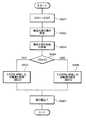
図1には、超音波探触子の製造プロセスの第1例がフローチャートとして示されている。この超音波探触子は、生体を超音波診断する超音波診断装置に対してプローブケーブルを介して接続され、超音波の送受波を行うことによりエコーデータを取り込むプローブである。ちなみに、この超音波探触子は、生体の表面上に当接して用いられるものであってもよいし、生体の体腔内に挿入して用いられるものであってもよい。以下に、その超音波探触子の製造プロセスを説明し、それに併せて、超音波探触子(特にアレイ振動子)の構造上の特徴について説明する。
【0039】
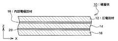
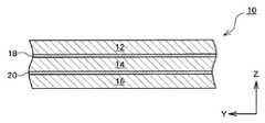
図1に示すS101の工程に先立って、図2に示すような分極済みの積層体(積層アッセンブリ)10が用意される。積層体10を構成する複数の部材はあらかじめ相互に接着されている。具体的には、積層体10は、図2に示されるように、全体として、平板状の形状を有し、具体的には、複数の圧電部材(圧電体)12,14,16を有する。それらの中で、隣接する2つの圧電部材12,14(14,16)の間に、水平電極部材としての内部電極部材18,20が設けられている。この積層体10における、X方向のサイズは例えば20mmであり、Y方向のサイズは例えば20mmであり、Z方向のサイズは例えば0.51mmである。ちなみに、圧電部材12,14,16の材料としては、公知のPZTなどの圧電材料をあげることができる。もちろん、それ以外の材料(例えば複合材料)で各圧電部材12,14,16を構成するようにしてもよい。なお、図2〜図9においては、図面における左右方向がX方向(第1水平方向)であり、図面における上下方向がZ方向(垂直方向)である。Z方向は超音波の送受波方向に相当する。
【0040】
図1に示されるS101では、図3に示されるように、複数の基礎溝22,24が形成される。具体的には、積層体10の上面10A側から、X方向に一定間隔2×Tをもって、複数の基礎溝(第1溝)22が形成される。この場合において、複数の基礎溝22におけるピッチは、複数の振動素子におけるピッチTの2倍とされる。上記と同様に、積層体10の下面10B側から、X方向に一定間隔2×Tをもって複数の基礎溝(第2溝)24が形成される。それらの複数の基礎溝24におけるピッチも複数の振動素子におけるピッチTの2倍である。ただし、複数の基礎溝22と複数の基礎溝24は、X方向において互い違いに形成されている。複数の基礎溝22及び複数の基礎溝24は、それぞれY方向に伸長した矩形の溝である。すなわち、それらの基礎溝22,24は互いに平行である。ここで、それらの基礎溝22,24の幅W1は、後述する特定構造(対向構造、隣合せ構造)(後の図9における符号200U,200Dを参照)を構築できる限りにおいて、適当な大きさに設定され、例えば、そのW1は0.08mmである。なお、積層体10は、一般に、積層されたn個の圧電部材によって構成され、ここでnは望ましくは奇数であり、特に望ましくは3である。
【0041】
また、各基礎溝22の深さL1は、上面10Aから見て2番目の内部電極部材20の手前までの深さとされ、例えばそのL1は0.3mmである。これは、各基礎溝24の深さL1についても同様であり、深さL1は下面10Bから見て2番目の内部電極体18の手前までの深さである。このような基礎溝22,24の形成により、内部電極体18は複数の要素18Aに分割され、これと同様に、内部電極体20も複数の要素20Aに分割される。ちなみに、基礎溝22,24を形成する場合には、例えばダイシングソーなどの切削加工器具を用いることができる。これは後述する各種の溝の形成に当たっても同様である。
【0042】
図1のS102では、図4に示されるように、S101で形成された複数の基礎溝22,24に対して、絶縁材26,28が充填される。この絶縁材26,28は、それを薄く形成した場合においても耐電圧レベルの高い材料であるのが望ましく、例えばポリイミド樹脂やエポキシ樹脂などの熱硬化性樹脂などを用いることができる。図4においては、基礎溝22に充填された絶縁材が符号26で示されており、一方、基礎溝24に充填された絶縁材が符号28で示されている。
【0043】
図1のS103では、図5に示されるように、各基礎溝22,24に対応してそれぞれ切削溝(第3溝30,第4溝32)が形成される。具体的には、図5において、各基礎溝22に充填された絶縁材料26に対して、その中央部を突き抜けるように切削溝30が切削加工により形成される。これと同様に、各基礎溝24に充填された絶縁材28に対しても、その中央部を貫くように切削溝(連絡溝、第4溝)32が形成される。ここで、各切削溝30,32の幅W2は上記の基礎溝22,24の幅W1よりも小さく、例えば0.04mmである。また切削溝30の深さL2は、基礎溝22の深さL1を超えてさらに上面から2番目の内部電極部材20を切断する深さとして設定され、例えばL2は0.36mmである。これは切削溝32についても同様であり、下面側から2番目の内部電極部材18を貫くようにその深さL2が設定されている。それらの切削溝30,32の形成により、各基礎溝22,24の内部には、図示のように、その溝内の各側面に一定の厚みで垂直方向に広がる面状の側面絶縁層(垂直絶縁層)26A,26B,28A,28Bが残存することになる。後に図9等で示すように、各側面絶縁層は、圧電部本体の各側面と各垂直電極層との間に配置される部材となる。また、それらの切削溝30,32の形成より、上述した各部分18A,20A(図5参照)はさらに二分割されることになり、具体的には、水平電極層としての複数の内部電極層18B,20Bが形成される。S102〜S103は、CVD法などによる絶縁膜の形成工程として置き換えることもできる。
【0044】
なお、図5に示す工程において、各切削溝30,32の深さをあまり大きくすると、積層体10自体が分断されてしまうため、そのような分断が生じない程度に各切削溝30,32の深さL2を設定するのが望ましい。
【0045】
図1に示すS104では、図6に示すように、各切削溝30,32の内部における各側面上に面状の導電膜34,36が形成される。この導電膜34,36は例えば無電解メッキ法や蒸着法などを利用して形成することができる。各導電膜34,36は、最終的に、一対の垂直電極層(側面電極層など)をなすものである。図6に示す段階においては、導電膜34が内部電極層20Bに対してコンタクト部100を介して電気的に接続されており、一方、導電膜34は内部電極層18Bに対して垂直絶縁層26A,26Bにより絶縁されている。これは導電膜36についても同様であり、その導電膜36はコンタクト部102によって内部電極層18Bに電気的に接続されている。なお、図6に示す工程において、切削溝30,32内に導電性部材を充填し、必要な切削加工を行うことにより、導電膜34,36を形成するようにしてもよい。
【0046】
図1に示すS105では、図7に示すように、各切削溝30,32の内部に、具体的には各導電膜34,36によって囲まれる空間内に、補強材38,40が充填される。この補強材38,40は導電膜34,36を覆ってそれらを保護する部材として機能する。補強材38,40は絶縁性を有する材料によって構成される。その補強材38,40は、熱硬化性をもった高分子材料、重合体材料、樹脂材料などを用いて構成するのが望ましい。なお、補強材38,40が複合化のための材料として用いられてもよく、それに関しては後に詳述する。
【0047】
図1に示すS106では、図8に示されるように、まず、積層体10の上面10A及び下面10Bに対して、それらを平面にするための研磨加工が施される。そのような加工により、導電膜34,36の端面が上方又は下方へ向けて適正に露出することになる。その後、スパッタ法や蒸着法などを利用して、上面10A及び下面10Bに対して、一定の厚みをもって、水平電極部材としての上面電極部材42及び下面電極部材44が形成される。この場合においては、各導電膜34の端面はコンタクト部104を介して上面電極部材42に電気的に接続され、これと同様に、各電極膜36の端面もコンタクト部106を介して下面電極部材44に電気的に接続される。
【0048】
図1のS107では、積層体10の下面側にバッキング51が接着される。後述するように、そのバッキング51は多数の信号線を内蔵したものであり、積層体10へのバッキング51の接着にあたっては例えば導電性接着剤などが利用される。
【0049】
そして、S108では、S107で形成された組立体(バッキング51付きの積層体10)に対し、図9及び図10に示されるように、複数の分離溝が切削加工により形成される。ここで、図10は、図9に示すA−A’断面を示すものであり、図10における左右方向はY方向であり、その上下方向はZ方向である。
【0050】
具体的には、上述した補強材38の中央部を貫通するように、幅W3をもって、上面側から複数の分離溝46,48がX方向に一定間隔で形成される。ここで、各分離溝(第5溝)46,48は、Y方向に伸長している。各分離溝46は、上面側に変位した各第1特定構造(第1対向構造)200Uに対して形成されるものであり、各分離溝48(第6溝)は、下面側に変位した各第2特定構造(第2対向構造)200Dに対して形成される。各特定構造200U,200Dについては、後に詳述するが、各特定構造200U,200Dは、分離溝46,48に対して左右対称構造を有する。ここで、それらの分離溝46,48の幅W3は、上記の補強材38の幅よりも小さく、例えばそのW3は、0.03mmである。また、それらの分離溝46,48の深さL3は、少なくとも、バッキング51における電極部材60を貫通する深さに設定され、例えば、そのL3は0.6mmである。
【0051】
図10に示すように、積層体10には、Y方向に並んだ複数の分離溝50も形成される。各分離溝50は、X方向に伸長している。各分離溝50の幅及び深さは、分離溝46,48の幅W3及び深さL3と同じである。ちなみに、複数の分離溝50は、複数の分離溝46,48の形成の前あるいは後に形成される。
【0052】
複数の分離溝46,48とは異なるサイズで複数の分離溝50を形成することも可能である。ただし、複数の分離溝50の形成に際しても、少なくとも積層体10及び電極部材60が切断される深さまで切削を行う必要がある。各分離溝46,48,50に対して、絶縁材料、音響分離材料、補強材料などを充填するようにしてもよい。
【0053】
図9において、バッキング51について説明すると、そのバッキング51は、大別してバッキング材料52、その上面に設けられた電極部材60、及び、バッキング材料52内にマトリクス状に設けられた複数の信号線58によって構成される。複数の信号線58は、複数の振動素子の二次元配列に対応した配列で設けられている。各信号線58は、その内部のシグナルリードとして機能する芯材56と、それを取り囲む被覆層54と、によって構成される。
【0054】
以上のように、積層体10に対して、X方向に並んだ複数の分離溝46,48を形成し、且つ、積層体10に対して、Y方向に並んだ複数の分離溝50を形成すると、それによって、積層体10が複数の振動素子に分割される。その状態では、図2に示した圧電部材12は、複数の圧電層12Aに分割されており、これと同様に、圧電部材14,16についても、それぞれ複数の圧電層14A,16Aに分割されている。また、図2に示した内部電極部材18,20についても、複数の内部電極層18B,20Bに分割されている。また、上述したように、バッキング51における電極部材60も複数に分割され、これにより複数の電極パッド60Aが構成されている。電気的な接続関係については後に図12を用いて説明する。
【0055】
図11には、図9に示すB−B’断面が示されている。上述したように、複数の分離溝46(あるいは48)の形成により、X方向(図中の左右方向)に隣接する振動素子ペアごとに、そのペアを構成する2つの振動素子の端部に跨って、特定構造200が形成される。特定構造200としては、グランド用の第1特定構造200Uと、シグナル用の第2特定構造200Dとがある(図9参照)。それらの特定構造200U,200Dは、互いに上下対称の関係にある。また、それらの特定構造200U,200Dは、それぞれが、その中心面(具体的には、分離溝46,48の中心に仮想的に存在する垂直面)に対して面対称の構造を有する。
【0056】
図11に示すように、特定構造200は、一方側振動素子に形成された垂直電極層(側面電極層)34Aと、他方側振動素子に形成された垂直電極層(側面電極層)34Bと、それらの垂直電極層34A,34Bの間に存在するギャップ領域と、を有する。より詳しくは、特定構造200は、一方側振動素子に形成された垂直絶縁層26A、垂直電極層34A及び側面補強層38Aと、他方側振動素子に形成された垂直絶縁層26B、垂直電極層34B及び側面補強層38Bと、側面補強層38A,38Bの間に存在する分離溝46と、で構成される。この例では、ギャップ領域は、側面補強層38A,38B及び分離溝46,48を合わせた領域として定義される。後述する他の例では、ギャップ領域は、複合化用の充填層、及び分離溝46を合わせた領域として定義される。
【0057】
図1におけるS109では、以上のように複数の振動素子からなるアレイ振動子が形成された後、そのアレイ振動子の上面側に例えば銅箔などによって構成されるグランド電極部材が設けられ、更に、その上に二次元配列された複数の整合層が設けられる。そのように形成された組立体が図示されていない探触子ケース内に配置される。
【0058】
図12には、アレイ振動子における電気的な接続関係が模式的に示されている。ここで、振動素子202,204に着目する。振動素子202,204はそれらの間を境として互いに対称の構造を有している。振動素子202においては、上方から奇数番目に存在する上面電極層42A及び内部電極層20Bに対して、垂直電極層34Bが電気的に接続されている。また、上方から偶数番目に存在する内部電極層18B及び下面電極層44Aに対して、垂直電極層36Aが電気的に接続されている。よって、下面電極層44Aにシグナルリードを接続し、上面電極層42Aにグランド電極部材を接続すれば、振動素子202をいわゆる積層型振動素子として機能させることができる。振動素子204においても、上記同様に、上方から奇数番目に存在する上面電極層42A及び内部電極層20Bに対して、垂直電極層34Aが電気的に接続されている。また、上方から偶数番目に存在する内部電極層18B及び下面電極層44Aに対して、垂直電極層36Bが電気的に接続されている。
【0059】
振動素子202における垂直電極層36Aと、振動素子204における垂直電極層36Bは対称関係にあるためにその製作は容易である。また、振動素子202における垂直電極層36Aと、振動素子204における垂直電極層36Bは近接対向しているが、互いに同じ極性を有しているので、絶縁性の面で有利である。
【0060】
上記実施形態に係る超音波探触子によれば、積層型振動素子を利用することができるので、電気的なインピーダンスを低減することができ、また垂直電極層を利用するので振動素子における振動面積のロスあるいは振動効率の低下といった問題を軽減又は解消することができる。すなわち高感度化を図ることが可能となる。さらに、上述した製造プロセスによれば、2種類の特定構造を互い違いに設定して、各積層型振動素子に対して確実に電気的接続を行える。更に、対向する2つの垂直電極層の極性が同じであるので、シグナルラインとグランドラインとの間の耐電圧レベルを上げることができる。
【0061】
以下に、超音波探触子の製造プロセスの他の幾つかの例について説明する。以下に説明する各製造プロセスは、上記製造プロセスと同様に、複数の特定構造を構築する工程を有し、一方、上記製造プロセスとは異なり、積層体を複合化する工程を有する。なお、それぞれの例において、同様の構成には同一符号を付することにする。
【0062】
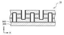
まず、図13〜図20を用いて、超音波探触子の製造プロセスの第二例について説明する。この例は、積層体に対する複合化を前もって行うことを特徴としている。
【0063】
図13には、製造プロセスがフローチャートとして示されている。S201では、積層体が複合化される。これを具体的に説明する。図14には積層体10が示されている。この積層体10は、図2に示した積層体10と同一であるが、図14と図2とでは、断面の方向が異なっている。図15に示すように、積層体10の下面側に、接着材料302を利用してベース部材300が接合される。次に、図16に示すように、積層体10に対して、その上面側から複数の複合化用の溝304がY方向に一定間隔をもって形成される。その溝304の深さは、積層体10の全体を越えて、ベース部材300が若干切削される程度である。複数の溝304の形成により、圧電部材12,14,16は複数の要素12B,14B,16Bに分割され、同時に、複数の内部電極部材18,20も複数の要素18B,20Bに分割される。この段階において、複数の圧電部305が形成される。各圧電部305は、垂直方向に積層された要素12B,14B,16B,18B,20Bで構成される。ベース部材300によって複数の圧電部305がバラバラに分離してしまう問題が防止されている。次に、複数の溝304に対して、充填材料としての樹脂材料が充填され、その樹脂材料を硬化させるために積層体10が加熱される。これにより、複数の樹脂層(樹脂部)306が形成される。樹脂材料は、例えば、エポキシ樹脂、シリコーン樹脂などを主成分とする複合化のための材料である。複数の樹脂層306が形成された後に、ベース部材300が積層体10から取り除かれる。その状態が図17に断面図として示されている。図17では、複合化された積層体が符号310で示されている。図18は積層体310の斜視図である。図18においては後に形成される複数の基礎溝22,24が破線で示されている。
【0064】
図13に示すS202では、図1に示したS101〜107の工程が実行される。次に、積層体310から、1Dアレイ振動子を作成する場合には、S203からS204の工程が実行され、一方、積層体310から、2Dアレイ振動子を作成する場合には、S203からS205の工程が実行される。
【0065】
S204の工程では、図19に示されるように、積層体310に対して、X方向に並んだ複数の分離溝46,48が形成される。各分離溝46,48はY方向に伸長する溝である。各分離溝46は、各特定構造(グランド用特定構造)200Uごとに、その中心位置に形成される。各分離溝48は、各特定構造(シグナル用特定構造)200Dごとに、その中心位置に形成される。図19における積層体310において、Y方向には、互い違いに複数の圧電部305及び複数の樹脂部306が結合している。X方向には、複数の振動素子310Aが並んでいる。そして、隣接する2つの振動素子ごとにそれらに跨って、特定構造200U又は200Dが構築されている。以上により、X方向をアレイ方向とし、かつY方向に積層された1Dアレイ振動子が構成される。
【0066】
一方、S205の工程では、図20に示されるように、積層体310に対して、X方向に並んだ複数の分離溝46,48と、Y方向に並んだ複数の分離溝50と、が形成される。各分離溝46,48はY方向に伸長する溝である。各分離溝50はX方向に伸長する溝である。それらの分離溝46,48,50の形成によって、二次元配列された複数の振動素子310Bが構成される。より詳しくは、各分離溝46は、各特定構造(グランド用特定構造)200Uごとに、その中心位置に形成される。各分離溝48は、各特定構造(シグナル用特定構造)200Dごとに、その中心位置に形成される。各分離溝50は、圧電部305又は樹脂部306のいずれかを二分割するように形成され、あるいは、圧電部305と積層部306の境界に形成される。図20に示す例では、各分離溝50によって、圧電部(全体)305が二分割され、これによって、Y方向の一方側振動素子に含まれる圧電部(一方側半分)305Aと、Y方向の他方側振動素子に含まれる圧電部305B(他方側半分)と、が形成されている。以上により、Y方向に複合化された2Dアレイ振動子が構成される。
【0067】
図13のS206では、図1のS109と同様に、積層体310に対して、他の部材が設けられる。なお、Y方向における圧電部及び樹脂部についての個数、サイズ及びピッチは任意に定めることができる。例えば、1つの振動素子に対して、より多くの個数の圧電部及び樹脂部を設けるようにしてもよい。図19及び図20においては、図9などに示されていた電極部材60、複数の信号線58などは図示省略されている。このことは、後に示す図22,23,31,32,34,35についても同様である。
【0068】
次に、図21〜図23を用いて、超音波探触子の製造プロセスの第三例について説明する。この例は、積層体に対する複合化を事後的に行うことを特徴としている。
【0069】
図21には、製造プロセスがフローチャートとして示されている。S301では、図1に示したS101〜S107の工程が実行される。S302では、複数の特定構造、上面電極部材及び下面電極部材が形成され、且つ、バッキングが接合された積層体に対して、Y方向に並んだ複数の複合化用の溝が形成される。ここで、その複数の複合化用の溝はそれぞれがX方向に伸長した溝である。S303では、複数の複合化用の溝に対して複合化用の樹脂材料が充填され、その樹脂材料は加熱により硬化される。
【0070】
S303の後、1Dアレイ振動子を形成する場合には、S304からS305が実行される。S305では、図22に示されるように、X方向に並ぶ複数の分離溝46,48が形成される。各分離溝46,48はY方向に伸長した溝である。これによって、X方向に並んだ複数の振動素子320Aが構成される。各振動素子320Aは、Y方向に交互に並んだ複数の圧電部326及び複数の樹脂部324によって構成される。各樹脂部324は、上述したように、複合化用の溝322に対して樹脂材料を充填することによって形成されたものである。上面電極部材42及び下面電極部材44を形成した後に、複数の溝322が形成されるために、上面電極層42及び下面電極層44も複数の溝322によって複数の電極層に切断される(図22には複数の上面電極層42Bが示されている)。よって、各樹脂層(樹脂部)324の上面325A及び下面325Bには、上面電極層及び下面電極層は設けられていない。
【0071】
一方、S303の後、2Dアレイ振動子を形成する場合には、S304からS306が実行される。S306では、図23に示されるように、X方向に並ぶ複数の分離溝46,48と、Y方向に並ぶ複数の分離溝50が形成される。各分離溝46,48はY方向に伸長した溝である。各分離溝50はX方向に伸長した溝である。これによって、X方向及びY方向の二次元に並んだ複数の振動素子320Bが構成される。各振動素子320Bは、Y方向に交互に並んだ少なくとも1つの圧電部326及び少なくとも1つの樹脂部324によって構成される。各樹脂部324は、上述したように、複合化用の溝322に対して樹脂材料を充填することによって形成されたものである。各分離溝50は、いずれかの圧電部又は樹脂部を二分する位置に形成され、あるいは、いずれかの圧電部及び樹脂部の境界位置に形成される。図23の例では、各圧電部が各分離溝50によって二分割され、これによって2つの圧電部326Aが形成されている。上面電極部材42及び下面電極部材44を形成した後に、複数の溝322が形成される点は、図22に示した例と同じである。図21のS307では、図22及び図23に示した複数の振動素子320に対して、他の部材が接合される。
【0072】
次に、図24〜図32を用いて、超音波探触子の製造プロセスの第四例について説明する。この例は、複数の特定構造の形成と同時に、積層体に対するX方向の複合化を行うことを特徴としている。
【0073】
図24には、製造プロセスがフローチャートとして示されている。S401では、図1に示したS101と同様に、積層体に対して複数の基礎溝が形成される。具体的には、図25に示す積層体10(図2に示した積層体10と同じ)に対して、その上面からX方向に一定の間隔で複数の幅広の基礎溝が形成され、その下面からX方向に一定の間隔で複数の幅広の基礎溝が形成される。それらの基礎溝の幅は、複合化のために必要な大きさに設定され、図3に示した通常の場合よりも、大きく設定される。
【0074】
次に、S402では、S102と同様に、各基礎溝の内部に絶縁材が充填され、その絶縁材が硬化される。S403では、S103と同様に、複数の切削溝が形成される。これによって、各基礎溝内に一対の垂直絶縁層が形成される。S404では、S104と同様に、各基礎溝の内面上に導電膜が形成される。その状態が図26に示されている。導電膜34,36は、垂直絶縁層26A,26B,28A,28Bの内面に形成されている。
【0075】
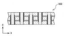
図24のS405では、図27に示すように、まず、積層体10の下面に対して接着材料302を用いてベース部材300が接合され、次に、各切削溝30,32を積層体10の全体にわたって貫通溝とするための加工が施される。すなわち、各切削溝30については、上から3番目の圧電部材16を部分的に切削する加工が施され、各切削溝32については、上から1番目の圧電部材12を部分的に切削する加工が施される。これによって、図28に示すように、積層体10に対して、複数の複合化用の溝329が形成される。また、S405では、それらの複合化用の溝329に対して、複合化のための樹脂材料330が充填され、その樹脂材料330が加熱されて硬化される。樹脂材料330は樹脂層つまり樹脂部を構成する。
【0076】
図24のS406では、図29に示すように、ベース部材300が積層体10から取り除かれる。これにより、複合化された積層体332が得られる。次に、図30に示すように、積層体332に対して、上面電極部材42及び下面電極部材44が形成される。また、下面電極部材44に対してバッキングが接着される。
【0077】
1Dアレイ振動子(タイプA)を形成する場合には、S407からS408が実行される。S408では、複数の特定構造の中心位置に対応して、X方向に並んだ複数の分離溝46,48が形成される。これによって、図31に示すように、複数の振動素子332AがX方向に並んだ1Dアレイ振動子が構成される。図31における符号334は1つの振動素子332Aを示し、符号336は圧電部を示している。符号338は、圧電部336の両隣に形成された一対の樹脂部を示している。このように、各振動素子332Aは、X方向に複合化されている。
【0078】
一方、1Dアレイ振動子(タイプB)を形成する場合には、S407からS409が実行される。S409では、Y方向に並んだ複数の分離溝50が形成される。各分離溝50はX方向に伸長した溝である。これによって、図32に示すように、複数の振動素子332BがY方向に並んだ1Dアレイ振動子が構成される。各振動素子332Bは、その長手方向がX方向であり、その方向に複合化されている。図32において、第1の観点から見れば、各振動素子332Bは、複数の要素(区分に相当)340,341を連結した部材である。隣接する2つの要素340,341に跨って特定構造200U’又は200D’が形成されており、その特定構造200U’又は200D’は中央部分に樹脂層(樹脂部)344を有する。この図32に示す例では、樹脂層344は分離溝を有していないが、観念的には、樹脂層344は、一方側の部分340に属する部分343Aと、他方側の部分341に属する部分343Bとに分けられる。第2の観点から見れば、各振動素子332Bは、X方向に互い違いに設けられた複数の圧電部342及び複数の樹脂部344を連結した部材である。
【0079】
他方、2Dアレイ振動子を形成する場合には、S407からS410が実行される。S410では、複数の特定構造の中心位置に対応して、X方向に並んだ複数の分離溝が形成され、また、Y方向に並んだ複数の分離溝が形成される。これによって、X方向に複合化された圧電体が、X方向及びY方向に整列した複数の振動素子に分割される。つまり、図31に示す圧電体332に対して、更に、Y方向に並んだ複数の分離溝(図10に示した複数の分離溝50に相当する)を形成することにより、複数の振動素子が構成される。図24のS411では整合層の形成など他の加工が施される。
【0080】
次に、図33〜図35を用いて、超音波探触子の製造プロセスの第五例について説明する。この例は、積層体に対するX方向及びY方向の複合化を特徴としている。
【0081】
図33には、製造プロセスのフローチャートが示されている。Y方向についての積層体に対する事前複合化を行う場合、S501からS502が実行され、次にS503が実行される。具体的には、S502では、図13に示したS201が実行され、圧電体に対してY方向の複合化を施す加工が実施される(図17及び図18参照)。そして、S503では、図24に示したS401〜S406の工程が実行され、X方向に並んだ複数の特定構造の構築と同時に、X方向に並んだ複数の樹脂層が形成される。これによって、X方向及びY方向の両方向に複合化された圧電体が構成される。
【0082】
一方、Y方向に事後複合化を行う場合、S501からS504が実行され、次にS505が実行される。具体的には、S504において、図24に示したS401〜S406の工程が実行され(図30参照)、次に、S505では、図21で示したS302及びS303と同様に、Y方向に複数の複合化用の溝が形成され、各溝に対して複合化用の樹脂材料が充填される。これによって、X方向及びY方向の両方向に複合化された圧電体が構成される。
【0083】
上記の二次元複合化の後、1Dアレイ振動子(タイプA)を形成する場合には、S506,S507を経て、S508が実行される。そのS508では、X方向に並んだ複数の分離溝が形成される。ここで、各分離溝はY方向に伸長した溝である。これによって、X方向に並んだ複数の振動素子が構成される。それらの複数の振動素子は、後に説明する図34に示される構成から、複数の分離溝50を除いたものに相当する。
【0084】
上記の二次元複合化の後、1Dアレイ振動子(タイプB)を形成する場合には、S506,S507を経て、S509が実行される。そのS509では、Y方向に並んだ複数の分離溝が形成される。ここで、各分離溝はX方向に伸長した溝である。これによって、Y方向に並んだ複数の振動素子が構成される。それらの複数の振動素子は、後に説明する図34に示される構成から、複数の分離溝46,48を除いたものに相当する。
【0085】
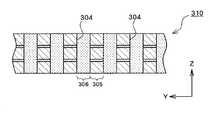
上記の二次元複合化の後、2Dアレイ振動子(タイプA)を形成する場合には、S506,S510を経て、S511が実行される。そのS511では、X方向に並んだ複数の分離溝が形成され、また、Y方向に並んだ複数の分離溝が形成される。これによって図34に示す二次元アレイ振動子が構成される。具体的には、二次元に複合化された積層体350に対して、X方向に複数の分離溝46,48が形成される。各分離溝46,48は、Y方向に伸長した溝であり、各特定構造200U,200Dごとに形成される。ある1つの振動素子350Aに着目した場合、その振動素子350Aは、X方向においては圧電区間336と、その両側に形成された2つの樹脂区間338とで構成される。符号334は、X方向における振動素子350Aの全幅を示している。その振動素子350Aは、Y方向においては、2つの圧電区間351と1つの樹脂区間352とで構成される。よって、上方から見て、振動素子350Aは、H形状を有する樹脂部と矩形の2つの圧電部とで構成される。図34に示す構成は一例であり、例えば、Y方向に所望数の圧電区間及び樹脂区間を設けるようにしてもよい。
【0086】
上記の二次元複合化の後、2Dアレイ振動子(タイプB)を形成する場合には、S506,S510を経て、S512が実行される。そのS512では、X方向に並んだ複数の分離溝が間引き形成され、また、Y方向に並んだ複数の分離溝が間引き形成される。具体的には、二次元に複合化された積層体350に対して、X方向に複数の分離溝48が形成される。各分離溝48は、Y方向に伸長した溝であり、各特定構造200Dごとに形成される。つまり、図35に示す例では、各特定構造200U(図34参照)については分離溝46は形成されていない。もちろん、複数の特定構造の並びの中で、図35に示すように1つおきの特定構造に対して分離溝を形成するのではなく、m(mは2以上)個おきの特定構造に対して分離溝を形成するようにしてもよい。一方、複数の分離溝50は、任意の間隔で形成することができ、Y方向について、1つの振動子当たり、より多くの圧電区間351及び樹脂区間352を設けるようにしてもよい。
【0087】
図35に示す例では、ある1つの振動素子350Bに着目した場合、その振動素子350Bは、X方向においては、2つの圧電区間402と、それらの圧電区間402に挟まれる樹脂区間406と、2つの圧電区間の両側に設けられた2つの樹脂区間404と、で構成される。符号400は、X方向における振動素子350Bの全幅を示している。その振動素子350Bは、Y方向においては、3つの圧電区間351と、2つの樹脂区間352とで構成される。よって、上方から見て、振動素子350Bは、6(=2×3)個の圧電部と、それらの圧電部の間に存在する格子形状をもった樹脂部と、で構成される。図35に示す構成は一例であり、例えば、X方向及びY方向に、より多くの圧電区間、樹脂区間を設定するようにしてもよい。
【0088】
図35に示す例では、X方向について、隣接する2つの振動素子の間に特定構造200Dが形成され、また振動素子350Bの中央部に特定構造200U’が形成されている。特定構造(素子間の特定構造)200Dと特定構造(素子内部の特定構造)200U’とを対比した場合、素子間の特定構造200Dが分離溝46を有するのに対し、素子内部の特定構造200U’が分離溝を有しない点で異なる。しかし、素子間の特定構造200Dと素子内部の特定構造200U’は、同極性をもった面対称な一対の垂直電極層を有する点で共通する。特に、両者は、絶縁性を良好にできる点、構造の構築が容易である点、で共通する。
【0089】
上記の第二例〜第五例によれば、積層化及び複合化されたアレイ振動子を実現できる。特に、積層化の後に複合化を行うので、垂直方向に並ぶ各部材間において水平方向の位置決め誤差を排除できる。また、その複合化も溝形成及び材料充填によって行えるので容易に実現できる。
【0090】
【発明の効果】
以上説明したように、本発明によれば、新しい構造及び良好な性能を有するアレイ振動子を提供でき、また、そのための効率的な製造方法を提供できる。
【図面の簡単な説明】
【図1】 超音波探触子の製造プロセスの第一例を説明するためのフローチャートである。
【図2】 積層体を示す断面図である。
【図3】 基礎溝が形成された積層体を示す断面図である。
【図4】 絶縁材料が充填された積層体を示す断面図である。
【図5】 切削溝が形成された積層体を示す断面図である。
【図6】 導電膜が形成された積層体を示す断面図である。
【図7】 補強材が充填された積層体を示す断面図である。
【図8】 上面電極部材及び下面電極部材が設けられた積層体を示す断面図である。
【図9】 アレイ振動子のX−Z断面を示す断面図である。
【図10】 アレイ振動子のY−Z断面を示す断面図である。
【図11】 図9に示すB−B’断面を示す断面図である。
【図12】 各振動素子における電気的な接続関係を説明するための模式図である。
【図13】 超音波探触子の製造プロセスの第二例を説明するためのフローチャートである。
【図14】 積層体を示す断面図である。
【図15】 ベース部材が暫定的に接合された積層体を示す断面図である。
【図16】 複数の複合化用溝が形成された積層体を示す断面図である。
【図17】 樹脂材料が充填された後の積層体を示す断面図である。
【図18】 Y方向に複合化された積層体を示す斜視図である。
【図19】 Y方向に複合化された積層型1Dアレイ振動子を示す斜視図である。
【図20】 Y方向に複合化された積層型2Dアレイ振動子を示す斜視図である。
【図21】 超音波探触子の製造プロセスの第三例を説明するためのフローチャートである。
【図22】 上面電極部材及び下面電極部材を設けた後に積層体に対してY方向に複合化を行うことにより製作された積層型1Dアレイ振動子を示す斜視図である。
【図23】 上面電極部材及び下面電極部材を設けた後に積層体に対してY方向に複合化を行うことにより製作された積層型2Dアレイ振動子を示す斜視図である。
【図24】 超音波探触子の製造プロセスの第四例を説明するためのフローチャートである。
【図25】 積層体を示す断面図である。
【図26】 基礎溝、絶縁材料及び導電膜が形成された積層体を示す断面図である。
【図27】 ベース部材が暫定的に接合された積層体を示す断面図である。
【図28】 複合化用の樹脂材料が充填された積層体を示す断面図である。
【図29】 ベース部材が取り外された積層体を示す断面図である。
【図30】 上面電極部材及び下面電極部材が設けられた積層体を示す断面図である。
【図31】 X方向に複合化され、X方向に分離された積層型1Dアレイ振動子を示す図である。
【図32】 X方向に複合化され、Y方向に分離された積層型2Dアレイ振動子を示す図である。
【図33】 本発明に係る製造プロセスの第五例を説明するためのフローチャートである。
【図34】 X方向及びY方向に複合化された積層型2Dアレイ振動子の一例を示す斜視図である。
【図35】 X方向及びY方向に複合化された積層型2Dアレイ振動子の他の例を示す斜視図である。
【符号の説明】
10 積層体、12,14,16 圧電部材、18,20 内部電極部材、22,24 基礎溝、26,28 絶縁材料、26A,26B 垂直絶縁層、34A,34B 垂直電極層、38A,38B 側面補強層、30,32 切削溝、34,36 導電膜、38,40 補強材、42 上面電極部材、44 下面電極部材、46,48,50 分離溝、51 バッキング、200U,200U’ グランド用の第1特定構造、200D,200D’ シグナル用の第2特定構造、305,326,336,342,351,402 積層型圧電部、306,324,338,343,352,404 樹脂部、310,332 複合化された積層体、330 樹脂材料。[0001]
BACKGROUND OF THE INVENTION
The present invention relates to an ultrasonic probe and a manufacturing method thereof, and more particularly to a structure of a stacked array transducer used in ultrasonic diagnosis of a living body and a manufacturing method thereof.
[0002]
[Prior art and problems]
As array transducers in which a plurality of transducer elements are arranged, 2D array transducers (including sparse 2D array transducers), 1.5D array transducers, and the like are known. In such an array vibrator, the size of each vibration element constituting the vibrator is very small. For this reason, the electrical impedance of each vibration element becomes extremely high, and electrical impedance matching cannot be achieved between each vibration element and the cable (or the apparatus main body). As a result, the problem of significant sensitivity loss occurs.
[0003]
In view of this, a technique has been proposed in which each vibration element is a laminated type. According to this technique, each vibration element is configured as a stacked body in which a plurality of piezoelectric layers and a plurality of electrode layers are stacked in a predetermined order. Specifically, a lower electrode layer is provided on the lower surface of the multilayer body, an upper electrode layer is provided on the upper surface of the multilayer body, and an internal electrode layer is provided between two adjacent piezoelectric layers. The odd-numbered electrode layers in the plurality of electrode layers are, for example, signal electrode layers, and the even-numbered electrode layers are, for example, ground electrode layers. A voltage signal is applied between the plurality of signal electrode layers and the plurality of ground electrode layers. According to this configuration, the electrical impedance of the vibration element can be lowered.
[0004]
For the laminated vibration element as described above, electrical connection to a plurality of electrode layers becomes a problem. In particular, how to connect leads or electrode layers to a plurality of internal electrode layers becomes a problem. As one conventional example, there is a method using a via (for example, a thin conductive line that vertically passes through the center of the vibration element). However, the area of the vibration element is very small, and there is a problem that it is difficult to manufacture the element afterwards, which is not practical.
[0005]
In this regard,
[0006]
[Patent Document 1]
JP 2001-29346 A
[0007]
An object of the present invention is to provide an ultrasonic probe including a stacked array transducer having good performance and a method for manufacturing the same.
[0008]
Another object of the present invention is to facilitate the manufacture of an ultrasonic probe including a stacked array transducer.
[0009]
[Means for Solving the Problems]
(1) An ultrasonic probe according to the present invention includes a stacked ultrasonic transducer having a first portion and a second portion adjacent to each other, and the first portion and the second portion are each vertical. A plurality of first horizontal electrode layers and a plurality of second horizontal electrode layers provided alternately in a direction; a first vertical electrode layer electrically connected to the plurality of first horizontal electrode layers; A second vertical electrode layer electrically connected to the second horizontal electrode layer, the first vertical electrode layer included in the first portion, and the first vertical electrode layer included in the second portion. Are adjacent to each other through the first gap region and have the same polarity, and the ultrasonic transducer includes a first vertical electrode layer included in the first portion and a first vertical electrode layer included in the second portion. And the first gap region.
[0010]
In the above configuration, the ultrasonic transducer is a 1D array transducer, a 1.5D array transducer, a 2D array transducer, or the like. The first part and the second part are formed adjacent to each other in the horizontal direction, and are laminated. In other words, the first portion and the second portion correspond to two adjacent laminated vibration elements, or correspond to two sections or blocks interconnected in the horizontal direction in a certain laminated vibration element. The first specific structure is formed across (or between) the first portion and the second portion. The first specific structure has a function of connecting a ground line or a signal line to a plurality of first horizontal electrode layers included in the first part and the second part. The first specific structure includes a pair of first vertical electrode layers (a first vertical electrode layer of a first portion and a first vertical electrode layer of a second portion) that are spaced apart from each other and face each other. Since the pair of first vertical electrode layers have the same polarity (ground or signal), there is an advantage that electrical performance can be improved, such as improvement in insulation. In the first gap region, a reinforcing layer, an insulating layer, a composite resin layer, an element isolation groove, and the like may be provided. Each vertical electrode layer functions as a side electrode, an internal electrode, or the like. Each vertical electrode layer is preferably formed in a planar form, but other forms may be employed. The array transducer may have a convex shape. In that case, the vertical direction is defined as the ultrasonic wave propagation direction for each vibration element.
[0011]
Preferably, the ultrasonic transducer further includes a third portion adjacent to the second portion, and the third portion includes a plurality of first horizontal electrode layers and a plurality of first horizontal electrode layers provided alternately in the vertical direction. A second horizontal electrode layer; a first vertical electrode layer that electrically connects the plurality of first horizontal electrode layers; and a second vertical electrode layer that electrically connects the plurality of second horizontal electrode layers; The second vertical electrode layer included in the second portion and the second vertical electrode layer included in the third portion are adjacent to each other through the second gap region and have the same polarity, and the ultrasonic vibration The child further has a second specific structure including a second vertical electrode layer included in the second portion, a second vertical electrode layer included in the third portion, and the second gap region.
[0012]
In the above configuration, the first portion, the second portion, and the third portion are formed side by side in the horizontal direction. A first specific structure is formed across (or between) the first part and the second part, and a second specific structure is formed across (or between) the second part and the third part Is done. The first specific structure and the second specific structure have different polarities. Also in the second specific structure, as in the first specific structure, the pair of second vertical electrode layers included in the second specific structure face each other through the second gap region and have the same polarity.
[0013]
Preferably, each of the first specific structure and the second specific structure is a symmetrical structure in the horizontal direction. Preferably, the first specific structure and the second specific structure are in a mutually inverted relationship in the vertical direction.
[0014]
The specific structure (the first specific structure and the second specific structure) has a pair of vertical electrode layers having the same polarity that are close to each other and face each other. From this point of view, the specific structure can also be expressed as “opposing structure” or “adjacent structure”. Although the specific structure can be constructed as an asymmetric structure in the horizontal direction, it is desirable to construct it as a symmetric (plane-symmetric) structure or a mirror structure in the horizontal direction in order to simplify its manufacture. Each specific structure can be easily manufactured by repeating, for example, groove formation and material filling.
[0015]
In the above configuration,The first portion, the second portion, and the third portion each further include a plurality of first horizontal electrode layers, a plurality of second horizontal electrode layers, and a plurality of piezoelectric layers.BodyAnd the piezoelectric partBodyOne side of(First side)The plurality of second horizontal electrode layers formed onInternal electrode layer inThe first vertical electrodelayerFirst insulating means for insulating the piezoelectric portion and the piezoelectric portionBodyThe other side of(Second side)The plurality of first horizontal electrode layers formed onInternal electrode layer inAnd a second insulating means for insulating the second vertical electrode layer.Here, each insulating means is configured as a planar insulating layer extending in the vertical direction.
[0016]
According to the above configuration, the firstVertical insulation layerAnd secondVertical insulation layerCan provide the necessary insulation for each polarity of the signal and ground, and can occur due to the pair of vertical electrode layers, more precisely,LaminatedDisturbance and distortion of the electric field in the piezoelectric part main body) composed of a plurality of piezoelectric layers and a plurality of horizontal electrode layers can be prevented or reduced. Therefore, the electromechanical conversion efficiency in the piezoelectric portion can be improved.
[0017]
Preferably, the first vertical electrode layer included in the first part, the second part, and the third part is one of a ground vertical electrode layer and a signal vertical electrode layer, and the first part, the second part, The second vertical electrode layer included in the portion and the third portion is the other of the ground vertical electrode layer and the signal vertical electrode layer, and the first specific structure includes a ground specific structure and a signal specific structure. The second specific structure is the other of the ground specific structure and the signal specific structure.
[0018]
Preferably, the ultrasonic transducer is an array transducer, the first gap region and the second gap region each have a separation groove, and the first portion, the second portion, and the third portion are: Each is a vibration element constituting the array vibrator. Preferably, each of the first part, the second part, and the third part is stacked in the vertical direction and combined in the horizontal direction.
[0019]
The above-described combination can provide one or more advantages such as the acoustic impedance of each vibration element can be adjusted (desirably reduced) and the frequency band can be adjusted (desirably expanded). Preferably, the compounding direction is a first horizontal direction as an arrangement direction of the first part, the second part, and the third part, a second horizontal direction orthogonal thereto, or a first horizontal direction and a first horizontal direction. 2 both directions in the horizontal direction.
[0020]
Preferably, the ultrasonic transducer is an array transducer, the array transducer has a plurality of vibration elements, and each vibration element has the first portion, the second portion, and the third portion. . Preferably, the vibration elements are stacked in the vertical direction and combined in the element longitudinal direction. The element longitudinal direction is one horizontal direction, which is the X direction in the embodiments described later.
[0021]
Preferably, each of the first part, the second part, and the third part includes a piezoelectric part and a resin part connected in a horizontal direction, the piezoelectric part is laminated, and the resin part is formed by filling. Is done.
[0022]
(2) An ultrasonic probe according to the present invention includes an array transducer having a plurality of transducer elements, and each transducer element includes a plurality of first horizontal electrode layers and a plurality of transducer elements provided alternately in the Z direction. A second horizontal electrode layer; a first vertical electrode layer electrically connected to the plurality of first horizontal electrode layers; and a second electrically connected to the plurality of second horizontal electrode layers. And the array transducer has a plurality of first specific structures and a plurality of second specific structures provided alternately in the X direction, and in each of the first specific structures, adjacent to each other The two first vertical electrode layers of the two vibrating elements are adjacent to each other via the first gap region, and in each of the second specific structures, the two second vertical electrode layers of the two adjacent vibrating elements are Adjacent through the second gap region.
[0023]
According to the above configuration, a plurality of first specific structures and a plurality of second specific structures are formed alternately in the X direction. Focusing on two vibrating elements adjacent in the X direction, the vertical electrode layer of the one-side vibrating element and the vertical electrode layer of the other-side vibrating element face each other through a gap region, but they have the same polarity. Therefore, there is an advantage in terms of insulation or voltage resistance.
[0024]
In the above configuration,Each vibration element further includes the plurality of second horizontal electrode layers.Internal electrode layer inFirst insulating means for electrically insulating the first vertical electrode layer with respect to the plurality of first horizontal electrode layersInternal electrode layer inAnd second insulating means for electrically insulating the second vertical electrode layer. here,The first insulating means has a first vertical insulating layer, and the second insulating means has a second vertical insulating layer.
[0025]
According to the above configuration, the plurality of second horizontal electrode layers are formed by the first insulating means.Internal electrode layer inThe first vertical electrode layer is insulated from the first horizontal electrode layer by the second insulating means.Internal electrode layer inTo the second vertical electrode layer. By the first insulating means and the second insulating means, it is possible to prevent or reduce the disturbance of the electric field inside the element, which may occur due to the presence of each vertical electrode layer.
[0026]
During the manufacturing process of the array vibrator, the polarization of the piezoelectric material may decrease or disappear due to a temperature rise or the like. In such a case, a repolarization step is additionally performed. When the repolarization step is performed, the first insulating means and the second insulating means described above make the polarization difficult to distort. This effect is greater as the relative dielectric constant of the material of the first insulating means and the second insulating means is smaller than the relative dielectric constant of the material of the vibration element. For example, the ratio is preferably about 1/1000.
[0027]
Preferably, a backing having a plurality of signal lines is provided on a lower surface side of the array transducer, and an end portion of the plurality of signal lines is arranged on the upper surface of the backing in accordance with the arrangement of the plurality of vibration elements. Are arranged. Preferably, a ground member and a matching layer are provided on the upper surface side of the array transducer.
[0028]
Preferably, each of the vibration elements has at least one piezoelectric portion and at least one resin portion connected in a Y direction orthogonal to the X direction. Preferably, each of the vibration elements includes at least one piezoelectric part and at least one resin part connected in the X direction. Preferably, each of the vibration elements includes a plurality of piezoelectric portions and a plurality of resin portions connected in the X direction and a Y direction orthogonal thereto. The resin portion is made of a polymer material, a polymer material, or the like. Moreover, it is desirable that the resin portion is made of a resin material that is filled and cured.
[0029]
(3) In the method of manufacturing an ultrasonic probe according to the present invention, a plurality of first grooves are formed from the upper surface side of a laminated body having a first internal electrode member and a second internal electrode member, and A step of forming a plurality of second grooves so as to be parallel to and alternately with the plurality of first grooves from the lower surface side, and on each side surface in each of the first grooves, the first Forming a first vertical electrode layer electrically connected to the internal electrode member and insulated from the second internal electrode member, thereby forming a plurality of first specific points corresponding to the plurality of first grooves; Forming a structure, and a second vertical electrode layer electrically connected to the second internal electrode member and insulated from the first internal electrode member on each side surface in the second groove Thereby forming a plurality of second specific structures corresponding to the plurality of second grooves. After the plurality of first specific structures and the plurality of second specific structures are formed, a plurality of separation grooves are formed in the stacked body, thereby dividing the stacked body into a plurality of vibration elements. And a step of performing.
[0030]
According to the above configuration, a plurality of first specific structures and a plurality of second specific structures can be manufactured alternately in a horizontal direction by a method of repeating groove formation and groove filling in a stacked body in a stepwise manner, thereby facilitating the manufacturing process. Or it is simplified and generation | occurrence | production of the positioning error of the horizontal direction between the laminated members can be prevented.
[0031]
Preferably, the method further includes a step of combining the stacked body in a horizontal direction before forming the plurality of first grooves and the plurality of second grooves. Preferably, the step of compounding the laminate in the horizontal direction includes a step of forming a plurality of composite grooves in the laminate, and a step of filling a filler in the plurality of composite grooves. including.
[0032]
Preferably, the step of forming the plurality of first specific structures and the plurality of second specific structures includes a step of compounding the stacked body in a horizontal direction. Preferably, the step of compounding the laminate in the horizontal direction includes a step of filling the plurality of first grooves and the plurality of second grooves with a compounding filling material.
[0033]
Preferably, the method further includes a step of compounding the stacked body in a horizontal direction after the step of constructing the plurality of first specific structures and the plurality of second specific structures. Preferably, the step of compounding the laminate in the horizontal direction includes a step of forming a plurality of compositing grooves in the laminate, and a step of filling a filling material into the plurality of compositing grooves. And including.
[0034]
The combined ultrasonic transducer generally has the advantage of widening the bandwidth, but has the problem that the electrical impedance increases and sensitivity decreases. By the above-described method, the ultrasonic transducers are compounded and stacked, thereby making it possible to reduce the electrical impedance of the ultrasonic transducers while broadening the bandwidth. Thereby, sensitivity can be improved. Moreover, since it is compounded after being laminated, the problem of the horizontal positioning error between the laminated members can be eliminated or reduced. As a result, the performance of the ultrasonic probe can be improved.
[0035]
(4) In the method of manufacturing an ultrasonic probe according to the present invention, a plurality of first grooves are formed at a first depth from the upper surface side of a laminated body having a first internal electrode member and a second internal electrode member. And a step of forming a plurality of second grooves at a second depth so as to be parallel to and alternately with the plurality of first grooves from the lower surface side of the stacked body. And a step of filling the plurality of first grooves and the plurality of second grooves with an insulating material and curing it, and a groove in which the hardened insulating material remains on each side surface in each of the first grooves. Forming a plurality of third grooves by cutting the insulating material in the plurality of first grooves at a third depth that is wider than the first depth and having a third depth greater than the first depth; and The plurality of second widths is a groove width in which the hardened insulating material remains on each side surface and a fourth depth deeper than the second depth. Forming a plurality of fourth grooves by cutting an insulating material therein, and forming a first vertical electrode layer electrically connected to the first internal electrode member on each side surface of each third groove And a second vertical electrode electrically connected to the second internal electrode member on each side surface in each of the fourth grooves. Forming a plurality of second specific structures with respect to the stacked body, and forming the plurality of first specific structures and the plurality of second specific structures; Forming a top electrode member on the top surface and forming a bottom electrode member on the bottom surface of the laminate; joining a backing to the bottom electrode member; and joining the backing after joining the backing. Dividing into a plurality of vibration elements.
[0036]
Preferably, in the step of forming the plurality of first specific structures, a reinforcing material or a composite is formed in the plurality of third grooves after the first vertical electrode layer is formed on each side surface in each of the third grooves. A step of filling the resin material for forming and curing the resin material, wherein the step of forming the plurality of second specific structures includes forming the second vertical electrode layer on each side surface in each of the fourth grooves. A step of filling the plurality of fourth grooves with a reinforcing material or a composite resin material and then curing the same is included.
[0037]
DETAILED DESCRIPTION OF THE INVENTION
Hereinafter, embodiments of the present invention will be described with reference to the drawings.
[0038]
FIG. 1 is a flowchart showing a first example of an ultrasonic probe manufacturing process. This ultrasonic probe is a probe that is connected to an ultrasonic diagnostic apparatus for ultrasonic diagnosis of a living body via a probe cable and takes in echo data by transmitting and receiving ultrasonic waves. Incidentally, this ultrasonic probe may be used in contact with the surface of a living body, or may be used by being inserted into a body cavity of a living body. Hereinafter, the manufacturing process of the ultrasonic probe will be described, and the structural features of the ultrasonic probe (particularly, the array transducer) will be described.
[0039]
Prior to the step of S101 shown in FIG. 1, a polarized laminated body (laminated assembly) 10 as shown in FIG. 2 is prepared. A plurality of members constituting the
[0040]
In S101 shown in FIG. 1, as shown in FIG. 3, a plurality of
[0041]
Further, the depth L1 of each
[0042]
In S102 of FIG. 1, as shown in FIG. 4, the insulating
[0043]
In S103 of FIG. 1, as shown in FIG. 5, cutting grooves (
[0044]
In the process shown in FIG. 5, if the depth of each cutting
[0045]
In S104 shown in FIG. 1, as shown in FIG. 6, planar
[0046]
In S105 shown in FIG. 1, as shown in FIG. 7, the reinforcing
[0047]
In S106 shown in FIG. 1, as shown in FIG. 8, first, polishing is performed on the
[0048]
In S <b> 107 of FIG. 1, the
[0049]
In S108, a plurality of separation grooves are formed by cutting as shown in FIGS. 9 and 10 for the assembly formed in S107 (the
[0050]
Specifically, a plurality of
[0051]
As shown in FIG. 10, the
[0052]
It is also possible to form the plurality of
[0053]
9, the
[0054]
As described above, when the plurality of
[0055]
FIG. 11 shows a B-B ′ cross section shown in FIG. 9. As described above, due to the formation of the plurality of separation grooves 46 (or 48), each vibration element pair adjacent in the X direction (left and right direction in the figure) straddles the ends of the two vibration elements constituting the pair. Thus, the
[0056]
As shown in FIG. 11, the
[0057]
In S109 in FIG. 1, after the array transducer composed of a plurality of transducer elements is formed as described above, a ground electrode member made of, for example, copper foil is provided on the upper surface side of the array transducer. A plurality of matching layers arranged two-dimensionally are provided thereon. The assembly so formed is placed in a probe case (not shown).
[0058]
FIG. 12 schematically shows an electrical connection relationship in the array transducer. Here, attention is paid to the
[0059]
Since the
[0060]
According to the ultrasonic probe according to the above-described embodiment, since the laminated vibration element can be used, the electrical impedance can be reduced, and since the vertical electrode layer is used, the vibration area in the vibration element can be reduced. Problems such as loss of vibration or reduction in vibration efficiency can be reduced or eliminated. That is, high sensitivity can be achieved. Furthermore, according to the manufacturing process described above, two types of specific structures can be set alternately so that electrical connection can be reliably made to each laminated vibration element. Furthermore, since the polarities of the two opposing vertical electrode layers are the same, the withstand voltage level between the signal line and the ground line can be increased.
[0061]
Hereinafter, some other examples of the manufacturing process of the ultrasonic probe will be described. Each manufacturing process described below has a step of constructing a plurality of specific structures, as in the above manufacturing process, and, unlike the manufacturing process, has a step of compositing a laminate. In each example, the same reference numerals are given to the same components.
[0062]
First, a second example of an ultrasonic probe manufacturing process will be described with reference to FIGS. This example is characterized in that the composite for the laminate is performed in advance.
[0063]
FIG. 13 shows a manufacturing process as a flowchart. In S201, the laminate is combined. This will be specifically described. FIG. 14 shows the laminate 10. Although this
[0064]
In S202 shown in FIG. 13, the steps S101 to S107 shown in FIG. 1 are executed. Next, when creating a 1D array transducer from the laminate 310, steps S203 to S204 are executed. On the other hand, when creating a 2D array transducer from the laminate 310, the steps from S203 to S205 are performed. The process is executed.
[0065]
In the step of S204, as shown in FIG. 19, a plurality of
[0066]
On the other hand, in the process of S205, as shown in FIG. 20, a plurality of
[0067]
In S206 of FIG. 13, other members are provided for the
[0068]
Next, a third example of an ultrasonic probe manufacturing process will be described with reference to FIGS. This example is characterized in that the composite of the laminate is performed afterwards.
[0069]
FIG. 21 shows a manufacturing process as a flowchart. In S301, steps S101 to S107 shown in FIG. 1 are executed. In S302, a plurality of composite grooves arranged in the Y direction are formed in the stacked body in which a plurality of specific structures, upper surface electrode members, and lower surface electrode members are formed and the backing is bonded. Here, each of the plurality of composite grooves is a groove extending in the X direction. In S303, a plurality of composite grooves are filled with a composite resin material, and the resin material is cured by heating.
[0070]
If a 1D array transducer is formed after S303, S304 to S305 are executed. In S305, as shown in FIG. 22, a plurality of
[0071]
On the other hand, when forming a 2D array transducer after S303, S304 to S306 are executed. In S306, as shown in FIG. 23, a plurality of
[0072]
Next, a fourth example of an ultrasonic probe manufacturing process will be described with reference to FIGS. This example is characterized in that the composite in the X direction is performed on the stacked body simultaneously with the formation of a plurality of specific structures.
[0073]
FIG. 24 shows the manufacturing process as a flowchart. In S401, as in S101 shown in FIG. 1, a plurality of basic grooves are formed in the stacked body. Specifically, a plurality of wide base grooves are formed at regular intervals in the X direction from the upper surface of the laminate 10 shown in FIG. 25 (same as the laminate 10 shown in FIG. 2), and the lower surface thereof. A plurality of wide basic grooves are formed at regular intervals in the X direction. The widths of these foundation grooves are set to a size necessary for compounding, and are set larger than the normal case shown in FIG.
[0074]
Next, in S402, as in S102, each base groove is filled with an insulating material, and the insulating material is cured. In S403, a plurality of cutting grooves are formed as in S103. Thereby, a pair of vertical insulating layers are formed in each basic groove. In S404, as in S104, a conductive film is formed on the inner surface of each basic groove. This state is shown in FIG. The
[0075]
In S405 of FIG. 24, as shown in FIG. 27, first, the
[0076]
In S406 of FIG. 24, the
[0077]
When a 1D array transducer (type A) is formed, S407 to S408 are executed. In S408, a plurality of
[0078]
On the other hand, when forming a 1D array transducer (type B), S407 to S409 are executed. In S409, a plurality of
[0079]
On the other hand, when forming a 2D array transducer, S407 to S410 are executed. In S410, a plurality of separation grooves arranged in the X direction are formed corresponding to the center positions of the plurality of specific structures, and a plurality of separation grooves arranged in the Y direction are formed. Thus, the piezoelectric body combined in the X direction is divided into a plurality of vibration elements aligned in the X direction and the Y direction. That is, by forming a plurality of separation grooves arranged in the Y direction (corresponding to the plurality of
[0080]
Next, a fifth example of an ultrasonic probe manufacturing process will be described with reference to FIGS. This example is characterized by a composite in the X and Y directions for the stack.
[0081]
FIG. 33 shows a flowchart of the manufacturing process. When pre-combination is performed on the stacked body in the Y direction, S501 to S502 are executed, and then S503 is executed. Specifically, in S502, S201 shown in FIG. 13 is executed, and a process of applying a composite in the Y direction to the piezoelectric body is performed (see FIGS. 17 and 18). In S503, the processes of S401 to S406 shown in FIG. 24 are executed, and a plurality of resin layers arranged in the X direction are formed simultaneously with the construction of a plurality of specific structures arranged in the X direction. Thus, a piezoelectric body that is compounded in both the X direction and the Y direction is configured.
[0082]
On the other hand, when post-compositing is performed in the Y direction, S501 to S504 are executed, and then S505 is executed. Specifically, in S504, steps S401 to S406 shown in FIG. 24 are executed (see FIG. 30). Next, in S505, as in S302 and S303 shown in FIG. Composite grooves are formed, and each groove is filled with a composite resin material. Thus, a piezoelectric body that is compounded in both the X direction and the Y direction is configured.
[0083]
In the case of forming a 1D array transducer (type A) after the above two-dimensional combination, S508 is executed through S506 and S507. In S508, a plurality of separation grooves arranged in the X direction are formed. Here, each separation groove is a groove extending in the Y direction. Thereby, a plurality of vibration elements arranged in the X direction are configured. The plurality of vibration elements correspond to a configuration obtained by removing the plurality of
[0084]
In the case of forming a 1D array transducer (type B) after the above two-dimensional combination, S509 is executed through S506 and S507. In S509, a plurality of separation grooves arranged in the Y direction are formed. Here, each separation groove is a groove extending in the X direction. Thus, a plurality of vibration elements arranged in the Y direction are configured. The plurality of vibration elements correspond to a configuration obtained by removing the plurality of
[0085]
In the case of forming a 2D array transducer (type A) after the above two-dimensional composite, S511 is executed through S506 and S510. In S511, a plurality of separation grooves arranged in the X direction are formed, and a plurality of separation grooves arranged in the Y direction are formed. Thus, the two-dimensional array transducer shown in FIG. 34 is configured. Specifically, a plurality of
[0086]
In the case of forming a 2D array transducer (type B) after the above two-dimensional composite, S512 is executed through S506 and S510. In S512, a plurality of separation grooves arranged in the X direction are thinned out, and a plurality of separation grooves arranged in the Y direction are thinned out. Specifically, a plurality of
[0087]
In the example shown in FIG. 35, when attention is paid to a
[0088]
In the example shown in FIG. 35, the
[0089]
According to the second to fifth examples, a stacked and complex array transducer can be realized. In particular, since compounding is performed after stacking, horizontal positioning errors can be eliminated between the members arranged in the vertical direction. In addition, the composite can be easily realized by forming the groove and filling the material.
[0090]
【The invention's effect】
As described above, according to the present invention, an array transducer having a new structure and good performance can be provided, and an efficient manufacturing method therefor can be provided.
[Brief description of the drawings]
FIG. 1 is a flow chart for explaining a first example of an ultrasonic probe manufacturing process.
FIG. 2 is a cross-sectional view showing a laminated body.
FIG. 3 is a cross-sectional view showing a laminated body in which a base groove is formed.
FIG. 4 is a cross-sectional view showing a stacked body filled with an insulating material.
FIG. 5 is a cross-sectional view showing a laminate in which cutting grooves are formed.
FIG. 6 is a cross-sectional view showing a stacked body on which a conductive film is formed.
FIG. 7 is a cross-sectional view showing a laminated body filled with a reinforcing material.
FIG. 8 is a cross-sectional view showing a laminate provided with an upper surface electrode member and a lower surface electrode member.
FIG. 9 is a cross-sectional view showing an XZ cross section of an array transducer.
FIG. 10 is a cross-sectional view showing a YZ cross section of an array transducer.
11 is a cross-sectional view showing a B-B ′ cross section shown in FIG. 9;
FIG. 12 is a schematic diagram for explaining an electrical connection relationship in each vibration element.
FIG. 13 is a flowchart for explaining a second example of the manufacturing process of the ultrasonic probe.
FIG. 14 is a cross-sectional view showing a laminated body.
FIG. 15 is a cross-sectional view showing a laminate in which base members are provisionally joined.
FIG. 16 is a cross-sectional view showing a laminate in which a plurality of composite grooves are formed.
FIG. 17 is a cross-sectional view showing the laminated body after being filled with a resin material.
FIG. 18 is a perspective view showing a laminated body combined in the Y direction.
FIG. 19 is a perspective view showing a stacked 1D array transducer compounded in the Y direction.
FIG. 20 is a perspective view showing a stacked 2D array transducer compounded in the Y direction.
FIG. 21 is a flowchart for explaining a third example of the manufacturing process of the ultrasonic probe;
FIG. 22 is a perspective view showing a stacked 1D array transducer manufactured by providing a composite body in the Y direction after providing an upper surface electrode member and a lower surface electrode member.
FIG. 23 is a perspective view showing a stacked 2D array transducer manufactured by providing a composite body in the Y direction after providing an upper surface electrode member and a lower surface electrode member.
FIG. 24 is a flowchart for explaining a fourth example of the manufacturing process of the ultrasonic probe;
FIG. 25 is a cross-sectional view showing a laminated body.
FIG. 26 shows the formation of a base groove, an insulating material, and a conductive film.LaminatedShowing the bodycross sectionFIG.
FIG. 27 is a cross-sectional view showing a laminate in which base members are provisionally joined.
FIG. 28 is a cross-sectional view showing a laminated body filled with a composite resin material.
FIG. 29 is a cross-sectional view showing the laminate from which the base member has been removed.
FIG. 30 is a cross-sectional view showing a laminate provided with an upper surface electrode member and a lower surface electrode member.
FIG. 31 is a diagram showing a stacked 1D array transducer that is composited in the X direction and separated in the X direction.
FIG. 32 is a diagram illustrating a stacked 2D array transducer that is composited in the X direction and separated in the Y direction.
FIG. 33 is a flowchart for explaining a fifth example of the manufacturing process according to the present invention.
FIG. 34 is a perspective view showing an example of a stacked 2D array transducer combined in the X direction and the Y direction.
FIG. 35 is a perspective view showing another example of a stacked 2D array transducer that is composited in the X and Y directions.
[Explanation of symbols]
10 laminated body, 12, 14, 16 piezoelectric member, 18, 20 internal electrode member, 22, 24 base groove, 26, 28 insulating material, 26A, 26B vertical insulating layer, 34A, 34B vertical electrode layer, 38A, 38B side reinforcement Layer, 30, 32 cutting groove, 34, 36 conductive film, 38, 40 reinforcement, 42 upper surface electrode member, 44 lower surface electrode member, 46, 48, 50 separation groove, 51 backing, first for 200U, 200U 'ground Specific structure, second specific structure for 200D, 200D ′ signal, 305, 326, 336, 342, 351, 402 Multilayer piezoelectric part, 306, 324, 338, 343, 352, 404 Resin part, 310, 332 Composite Laminated body, 330 resin material.
Claims (33)
Translated fromJapanese前記第1部分及び前記第2部分は、それぞれ、
垂直方向に互い違いに設けられた複数の第1水平電極層及び複数の第2水平電極層を有する圧電部本体と、
前記複数の第1水平電極層に対して電気的に接続される第1垂直電極層と、
前記複数の第2水平電極層に対して電気的に接続される第2垂直電極層と、
前記圧電部本体の第1側面と前記第1垂直電極層との間に設けられた垂直方向に広がる面状の絶縁層であって、前記複数の第2水平電極層における内部電極層に対して前記第1垂直電極層を絶縁する第1垂直絶縁層と、
前記圧電部本体の第2側面と前記第2垂直電極層との間に設けられた垂直方向に広がる面状の絶縁層であって、前記複数の第1水平電極層における内部電極層に対して前記第2垂直電極層を絶縁する第2垂直絶縁層と、
を有し、
前記第1部分が有する第1垂直電極層と、前記第2部分が有する第1垂直電極層と、が第1ギャップ領域を介して隣り合わせとなり且つ同じ極性を有し、
前記超音波振動子は、前記第1部分が有する第1垂直電極層及び第1垂直絶縁層と、前記第2部分が有する第1垂直電極層及び第1垂直絶縁層と、前記第1ギャップ領域と、で構成される第1特定構造を有し、
前記第1特定構造においては、前記第1ギャップ領域を中心として、前記第1部分が有する第1垂直電極層及び第1垂直絶縁層と、前記第2部分が有する第1垂直電極層及び第1垂直絶縁層と、が対称の位置関係にあることを特徴とする超音波探触子。A laminated ultrasonic transducer having a first portion and a second portion adjacent to each other;
The first part and the second part are respectively
A piezoelectric body having a plurality of first horizontal electrode layers and a plurality of second horizontal electrode layers provided alternately in the vertical direction;
A first vertical electrode layer electrically connected to the plurality of first horizontal electrode layers;
A second vertical electrode layer electrically connected to the plurality of second horizontal electrode layers;
A planar insulating layer extending between the first side surface of the piezoelectric body and the first vertical electrode layer and extending in the vertical direction, the internal electrode layer in the plurality of second horizontal electrode layers A first vertical insulating layer that insulates the first vertical electrode layer;
A planar insulating layer extending between the second side surface of the piezoelectric body and the second vertical electrode layer and extending in the vertical direction, the internal electrode layer of the plurality of first horizontal electrode layers A second vertical insulating layer for insulating the second vertical electrode layer;
Have
The first vertical electrode layer included in the first portion and the first vertical electrode layer included in the second portion are adjacent to each other through the first gap region and have the same polarity.
The ultrasonic transducer, wherein the first vertical electrode layerand the first vertical insulating layer first portion has a first vertical electrode layerand the first vertical insulating layer having said second portion, said first gap region When, in a first particular structure composedpossess,
In the first specific structure, the first vertical electrode layer and the first vertical insulating layer included in the first portion, and the first vertical electrode layer and the first portion included in the second portion, with the first gap region as a center. An ultrasonic probe characterized by having asymmetrical positional relationship with a vertical insulating layer .
前記超音波振動子は、更に、前記第2部分に隣接する第3部分を含み、
前記第3部分は、
前記垂直方向に互い違いに設けられた複数の第1水平電極層及び複数の第2水平電極層を有する圧電部本体と、
前記複数の第1水平電極層を電気的に接続する第1垂直電極層と、
前記複数の第2水平電極層を電気的に接続する第2垂直電極層と、
前記圧電部本体の第1側面と前記第1垂直電極層との間に設けられた垂直方向に広がる面状の絶縁層であって、前記複数の第2水平電極層における内部電極層に対して前記第1垂直電極層を絶縁する第1垂直絶縁層と、
前記圧電部本体の第2側面と前記第2垂直電極層との間に設けられた垂直方向に広がる面状の絶縁層であって、前記複数の第1水平電極層における内部電極層に対して前記第2垂直電極層を絶縁する第2垂直絶縁層と、
を有し、
前記第2部分が有する第2垂直電極層と、前記第3部分が有する第2垂直電極層と、が第2ギャップ領域を介して隣り合わせとなり且つ同じ極性を有し、
前記超音波振動子は、更に、前記第2部分が有する第2垂直電極層及び第2垂直絶縁層と、前記第3部分が有する第2垂直電極層及び第2垂直絶縁層と、前記第2ギャップ領域と、で構成される第2特定構造を有することを特徴とする超音波探触子。The ultrasonic probe according to claim 1,
The ultrasonic transducer further includes a third portion adjacent to the second portion,
The third part is
A piezoelectric body having a plurality of first horizontal electrode layers and a plurality of second horizontal electrode layers provided alternately in the vertical direction;
A first vertical electrode layer electrically connecting the plurality of first horizontal electrode layers;
A second vertical electrode layer electrically connecting the plurality of second horizontal electrode layers;
A planar insulating layer extending between the first side surface of the piezoelectric body and the first vertical electrode layer and extending in the vertical direction, the internal electrode layer in the plurality of second horizontal electrode layers A first vertical insulating layer that insulates the first vertical electrode layer;
A planar insulating layer extending between the second side surface of the piezoelectric body and the second vertical electrode layer and extending in the vertical direction, the internal electrode layer of the plurality of first horizontal electrode layers A second vertical insulating layer for insulating the second vertical electrode layer;
Have
The second vertical electrode layer included in the second portion and the second vertical electrode layer included in the third portion are adjacent to each other through the second gap region and have the same polarity.
The ultrasonic transducer further includes a second vertical electrode layerand the second vertical insulating layer having said second portion, and a second vertical electrode layerand the second vertical insulating layer in which the third portion has said second An ultrasonic probe having a second specific structure including a gap region.
前記第2特定構造においては、前記第2ギャップ領域を中心として、前記第2部分が有する第2垂直電極層及び第2垂直絶縁層と、前記第3部分が有する第2垂直電極層及び第2垂直絶縁層と、が対称の位置関係にあることを特徴とする超音波探触子。The ultrasonic probe according to claim 2,
In the second specific structure, the second vertical electrode layer and the second vertical insulating layer included in the second portion, the second vertical electrode layer and the second included in the third portion, with the second gap region as a center. An ultrasonic probe characterized by having asymmetrical positional relationship with a vertical insulating layer .
前記第1特定構造及び前記第2特定構造は、互いに垂直方向に反転した関係にあることを特徴とする超音波探触子。The ultrasonic probe according to claim 2,
The ultrasonic probe according to claim 1, wherein the first specific structure and the second specific structure are inverted in a vertical direction.
前記第1部分、前記第2部分及び前記第3部分は、それぞれ、更に、
前記第1垂直電極層上に形成された第1側面補強層と、
前記第2垂直電極層上に形成された第2側面補強層と、
を有することを特徴とする超音波探触子。The ultrasonic probe according to claim 2,
The first part, the second part, and the third part, respectively,
A first side reinforcing layer formed on the first vertical electrode layer;
A second side reinforcing layer formed on the second vertical electrode layer;
An ultrasonic probe characterized by comprising:
前記第1部分、前記第2部分及び前記第3部分が有する第1垂直電極層は、グランド垂直電極層及びシグナル垂直電極層の内の一方であり、
前記第1部分、前記第2部分及び前記第3部分が有する第2垂直電極層は、前記グランド垂直電極層及び前記シグナル垂直電極層の内の他方であり、
前記第1特定構造は、グランド用特定構造及びシグナル用特定構造の内の一方であり、
前記第2特定構造は、前記グランド用特定構造及び前記シグナル用特定構造の内の他方であることを特徴とする超音波探触子。The ultrasonic probe according to claim 2,
The first vertical electrode layer included in the first portion, the second portion, and the third portion is one of a ground vertical electrode layer and a signal vertical electrode layer,
A second vertical electrode layer included in the first portion, the second portion, and the third portion is the other of the ground vertical electrode layer and the signal vertical electrode layer;
The first specific structure is one of a ground specific structure and a signal specific structure,
The ultrasonic probe according to claim 2, wherein the second specific structure is the other of the ground specific structure and the signal specific structure.
前記超音波振動子は、水平方向に互い違いに並べられた複数の第1特定構造及び複数の第2特定構造を有することを特徴とする超音波探触子。The ultrasonic probe according to claim 2,
The ultrasonic transducer has a plurality of first specific structures and a plurality of second specific structures arranged alternately in a horizontal direction.
前記超音波振動子はアレイ振動子であり、
前記第1ギャップ領域及び前記第2ギャップ領域はそれぞれ分離溝を有し、
前記第1部分、前記第2部分及び前記第3部分は、それぞれ、前記アレイ振動子を構成する振動素子であることを特徴とする超音波探触子。The ultrasonic probe according to claim 2,
The ultrasonic transducer is an array transducer;
The first gap region and the second gap region each have a separation groove;
The ultrasonic probe, wherein each of the first part, the second part, and the third part is a vibration element constituting the array transducer.
前記第1部分、前記第2部分及び前記第3部分は、それぞれが、垂直方向に積層化され、且つ、水平方向に複合化されていることを特徴とする超音波探触子。The ultrasonic probe according to claim 2,
The ultrasonic probe according to claim 1, wherein the first portion, the second portion, and the third portion are stacked in the vertical direction and combined in the horizontal direction.
前記複合化の方向は、前記第1部分、前記第2部分及び前記第3部分の配列方向としての第1水平方向であることを特徴とする超音波探触子。The ultrasonic probe according to claim 9, wherein
The ultrasonic probe according to claim 1, wherein the compounding direction is a first horizontal direction as an arrangement direction of the first part, the second part, and the third part.
前記複合化の方向は、前記第1部分、前記第2部分及び前記第3部分の配列方向としての第1水平方向に直交する第2水平方向であることを特徴とする超音波探触子。The ultrasonic probe according to claim 9, wherein
The ultrasonic probe according to claim 1, wherein the compounding direction is a second horizontal direction orthogonal to a first horizontal direction as an arrangement direction of the first part, the second part, and the third part.
前記複合化の方向は、前記第1部分、前記第2部分及び前記第3部分の配列方向としての第1水平方向、及び、それに直交する第2水平方向の両方であることを特徴とする超音波探触子。The ultrasonic probe according to claim 9, wherein
The superposition direction is both a first horizontal direction as an arrangement direction of the first part, the second part, and the third part, and a second horizontal direction orthogonal thereto. Sonic probe.
前記超音波振動子はアレイ振動子であり、
前記アレイ振動子は複数の振動素子を有し、
前記各振動素子は、前記第1部分、前記第2部分及び前記第3部分を有することを特徴とする超音波探触子。The ultrasonic probe according to claim 2,
The ultrasonic transducer is an array transducer;
The array vibrator has a plurality of vibration elements,
Each of the vibrating elements includes the first portion, the second portion, and the third portion.
前記各振動素子は、垂直方向に積層化され、且つ、素子長手方向に複合化されたことを特徴とする超音波探触子。The ultrasonic probe according to claim 13,
The ultrasonic probe according to claim 1, wherein each of the vibration elements is laminated in a vertical direction and is compounded in a longitudinal direction of the element.
前記第1部分、前記第2部分及び前記第3部分は、それぞれ、水平方向に連結された圧電部及び樹脂部を含み、
前記圧電部は積層化され、
前記樹脂部は充填により形成されたことを特徴とする超音波探触子。The ultrasonic probe according to claim 2,
The first part, the second part, and the third part each include a piezoelectric part and a resin part connected in a horizontal direction,
The piezoelectric part is laminated,
The ultrasonic probe, wherein the resin portion is formed by filling.
前記各振動素子は、
Z方向に互い違いに設けられた複数の第1水平電極層及び複数の第2水平電極層を有する圧電部本体と、
前記複数の第1水平電極層に対して電気的に接続される第1垂直電極層と、
前記複数の第2水平電極層に対して電気的に接続される第2垂直電極層と、
前記圧電部本体の第1側面と前記第1垂直電極層との間に設けられた垂直方向に広がる面状の絶縁層であって、前記複数の第2水平電極層における内部電極層に対して前記第1垂直電極層を絶縁する第1垂直絶縁層と、
前記圧電部本体の第2側面と前記第2垂直電極層との間に設けられた垂直方向に広がる面状の絶縁層であって、前記複数の第1水平電極層における内部電極層に対して前記第2垂直電極層を絶縁する第2垂直絶縁層と、
を有し、
前記アレイ振動子は、X方向に互い違いに設けられた複数の第1特定構造及び複数の第2特定構造を有し、
前記各第1特定構造においては、隣接する2つの振動素子が有する2つの第1垂直電極層が第1ギャップ領域を介して隣り合わせとなり、
前記各第2特定構造においては、隣接する2つの振動素子が有する2つの第2垂直電極層が第2ギャップ領域を介して隣り合わせとなり、
前記各第1特定構造においては、前記第1ギャップ領域を中心として、一方の振動素子が有する第1垂直電極層及び第1垂直絶縁層と、他方の振動素子が有する第1垂直電極層及び第1垂直絶縁層と、が対称の位置関係にあり、
前記各第2特定構造においては、前記第2ギャップ領域を中心として、一方の振動素子が有する第2垂直電極層及び第2垂直絶縁層と、他方の振動素子が有する第2垂直電極層及び第2垂直絶縁層と、が対称の位置関係にあることを特徴とする超音波探触子。Including an array transducer having a plurality of transducer elements,
Each of the vibration elements is
A piezoelectric body having a plurality of first horizontal electrode layers and a plurality of second horizontal electrode layers provided alternately in the Z direction;
A first vertical electrode layer electrically connected to the plurality of first horizontal electrode layers;
A second vertical electrode layer electrically connected to the plurality of second horizontal electrode layers;
A planar insulating layer extending between the first side surface of the piezoelectric body and the first vertical electrode layer and extending in the vertical direction, the internal electrode layer in the plurality of second horizontal electrode layers A first vertical insulating layer that insulates the first vertical electrode layer;
A planar insulating layer extending between the second side surface of the piezoelectric body and the second vertical electrode layer and extending in the vertical direction, the internal electrode layer of the plurality of first horizontal electrode layers A second vertical insulating layer for insulating the second vertical electrode layer;
Have
The array transducer has a plurality of first specific structures and a plurality of second specific structures provided alternately in the X direction,
In each of the first specific structures, two first vertical electrodelayers of two adjacent vibration elements are adjacent to each other through the first gap region,
Wherein in each second particular structure,Ri second vertical electrodelayer of the two having two adjacent transducer elements Do a side by side through the second gapregion,
In each of the first specific structures, the first vertical electrode layer and the first vertical insulating layer included in one vibration element, and the first vertical electrode layer and the first vertical layer included in the other vibration element, with the first gap region as a center. 1 vertical insulating layer and a symmetrical positional relationship,
In each of the second specific structures, with the second gap region as a center, the second vertical electrode layer and the second vertical insulating layer included in one vibration element, and the second vertical electrode layer and the second vertical electrode layer included in the other vibration element An ultrasonic probe characterized in that thetwo vertical insulating layers are in a symmetrical positional relationship .
前記各振動素子は、更に、
前記第1垂直電極層上に形成された第1側面補強層と、
前記第2垂直電極層上に形成された第2側面補強層と、
を有することを特徴とする超音波探触子。The ultrasonic probe according to claim 16, wherein
Each vibration element further includes:
A first side reinforcing layer formed on the first vertical electrode layer;
A second side reinforcing layer formed on the second vertical electrode layer;
An ultrasonic probe characterized by comprising:
前記圧電部は奇数個の圧電層を有することを特徴とする超音波探触子。The ultrasonic probe according to claim 16, wherein
The ultrasonic probe according to claim 1, wherein the piezoelectric portion has an odd number of piezoelectric layers.
前記各振動素子の積層数は3であることを特徴とする超音波探触子。The ultrasonic probe according to claim 16, wherein
The ultrasonic probe according to claim 3, wherein the number of stacked layers of the vibration elements is three.
前記アレイ振動子の下面側には、複数の信号線を有するバッキングが設けられ、
前記バッキングの上面には、前記複数の振動素子の配列に合わせて、前記複数の信号線の端部が配列されたことを特徴とする超音波探触子。The ultrasonic probe according to claim 16, wherein
A backing having a plurality of signal lines is provided on the lower surface side of the array transducer,
An ultrasonic probe in which ends of the plurality of signal lines are arranged on the upper surface of the backing in accordance with the arrangement of the plurality of vibration elements.
前記アレイ振動子の上面側にはグランド部材及び整合層が設けられたことを特徴とする超音波探触子。The ultrasonic probe according to claim 16, wherein
An ultrasonic probe, wherein a ground member and a matching layer are provided on the upper surface side of the array transducer.
前記各振動素子は、前記X方向に直交するY方向に連結された少なくとも1つの圧電部及び少なくとも1つの樹脂部を有することを特徴とする超音波探触子。The ultrasonic probe according to claim 16, wherein
Each of the vibration elements has at least one piezoelectric part and at least one resin part connected in a Y direction orthogonal to the X direction.
前記各振動素子は、前記X方向に連結された少なくとも1つの圧電部及び少なくとも1つの樹脂部を有することを特徴とする超音波探触子。The ultrasonic probe according to claim 16, wherein
Each of the vibration elements has at least one piezoelectric part and at least one resin part connected in the X direction.
前記各振動素子は、前記X方向及びそれに直交するY方向に連結された複数の圧電部及び複数の樹脂部を有することを特徴とする超音波探触子。The ultrasonic probe according to claim 16, wherein
Each of the vibration elements has a plurality of piezoelectric parts and a plurality of resin parts connected in the X direction and a Y direction perpendicular thereto.
前記各第1溝内の各側面に、前記第1内部電極部材に対して電気的に接続され且つ前記第2内部電極部材に対して絶縁された第1垂直電極層を形成し、これによって前記複数の第1溝に対応して複数の第1特定構造を形成する工程と、
前記各第2溝内の各側面に、前記第2内部電極部材に対して電気的に接続され且つ前記第1内部電極部材に対して絶縁された第2垂直電極層を形成し、これによって前記複数の第2溝に対応して複数の第2特定構造を形成する工程と、
前記複数の第1特定構造及び前記複数の第2特定構造が形成された後に、前記積層体に対して複数の分離溝を形成し、これにより前記積層体を複数の振動素子に分割する工程と、
を含むことを特徴とする超音波探触子の製造方法。A plurality of first grooves are formed from the upper surface side of the multilayer body having the first internal electrode member and the second internal electrode member, and from the lower surface side, the plurality of first grooves are parallel to the plurality of first grooves. Forming a plurality of second grooves so as to be in an alternating relationship;
A first vertical electrode layer electrically connected to the first internal electrode member and insulated from the second internal electrode member is formed on each side surface in each of the first grooves. Forming a plurality of first specific structures corresponding to the plurality of first grooves;
A second vertical electrode layer electrically connected to the second internal electrode member and insulated from the first internal electrode member is formed on each side surface in each of the second grooves. Forming a plurality of second specific structures corresponding to the plurality of second grooves;
Forming a plurality of separation grooves in the stacked body after the plurality of first specific structures and the plurality of second specific structures are formed, thereby dividing the stacked body into a plurality of vibration elements; ,
A method for manufacturing an ultrasonic probe, comprising:
更に、前記複数の第1溝及び前記複数の第2溝を形成する前に、前記積層体を水平方向に複合化する工程を含むことを特徴とする超音波探触子の製造方法。26. The method of claim 25, wherein
Furthermore, before forming the plurality of first grooves and the plurality of second grooves, the method of manufacturing an ultrasonic probe further includes a step of compounding the stacked body in a horizontal direction.
前記積層体を水平方向に複合化する工程は、
前記積層体に対して複数の複合化用溝を形成する工程と、
前記複数の複合化用溝に対して充填材料を充填する工程と、
を含むことを特徴とする超音波探触子の製造方法。The method of claim 26.
The step of compounding the laminate in the horizontal direction includes:
Forming a plurality of composite grooves on the laminate;
Filling the plurality of composite grooves with a filling material;
A method for manufacturing an ultrasonic probe, comprising:
前記複数の第1特定構造及び前記複数の第2特定構造を形成する工程は、前記積層体を水平方向に複合化する工程を含むことを特徴とする超音波探触子の製造方法。26. The method of claim 25, wherein
The method of manufacturing an ultrasonic probe, wherein the step of forming the plurality of first specific structures and the plurality of second specific structures includes a step of compounding the stacked body in a horizontal direction.
前記積層体を水平方向に複合化する工程は、前記複数の第1溝及び前記複数の第2溝の中に複合化用の充填材料を充填する工程であることを特徴とする超音波探触子の製造方法。30. The method of claim 28, wherein
The step of compounding the laminated body in the horizontal direction is a step of filling the plurality of first grooves and the plurality of second grooves with a compounding filling material. Child manufacturing method.
更に、前記複数の第1特定構造及び前記複数の第2特定構造を構築する工程の後に、前記積層体を水平方向に複合化する工程を含むことを特徴とする超音波探触子の製造方法。26. The method of claim 25, wherein
Furthermore, after the step of constructing the plurality of first specific structures and the plurality of second specific structures, the method of manufacturing the ultrasonic probe further includes a step of compounding the laminate in the horizontal direction. .
前記積層体を水平方向に複合化する工程は、
前記積層体に対して複数の複合化用溝を形成する工程と、
前記複数の複合化用溝に対して充填材料を充填する工程と、
を含むことを特徴とする超音波探触子の製造方法。The method of claim 30, wherein
The step of compounding the laminate in the horizontal direction includes:
Forming a plurality of composite grooves on the laminate;
Filling the plurality of composite grooves with a filling material;
A method for manufacturing an ultrasonic probe, comprising:
前記積層体に対し、その下面側から、前記複数の第1溝と平行で且つそれらと互い違いの関係になるように、複数の第2溝を第2深さで形成する工程と、
前記複数の第1溝及び前記複数の第2溝に対して絶縁材料を充填し、それを硬化させる工程と、
前記各第1溝内の各側面に前記硬化した絶縁材料が残存する溝幅で、且つ、前記第1深さよりも深い第3深さで、前記複数の第1溝内の絶縁材料を切削して複数の第3溝を形成する工程と、
前記各第2溝内の各側面に前記硬化した絶縁材料が残存する溝幅で、且つ、前記第2深さよりも深い第4深さで、前記複数の第2溝内の絶縁材料を切削して複数の第4溝を形成する工程と、
前記各第3溝内の各側面に、前記第1内部電極部材に電気的に接続された第1垂直電極層を形成し、これによって前記積層体に対して複数の第1特定構造を形成する工程と、
前記各第4溝内の各側面に、前記第2内部電極部材に電気的に接続された第2垂直電極層を形成し、これによって前記積層体に対して複数の第2特定構造を形成する工程と、
前記複数の第1特定構造及び前記複数の第2特定構造が形成された後に、前記積層体の上面に上面電極部材を形成し、且つ、前記積層体の下面に下面電極部材を形成する工程と、
前記下面電極部材に対してバッキングを接合する工程と、
前記バッキングの接合後に、前記積層体を複数の振動素子に分割する工程と、
を含むことを特徴とする超音波探触子の製造方法。Forming a plurality of first grooves at a first depth from the upper surface side of the laminate having the first internal electrode member and the second internal electrode member;
Forming a plurality of second grooves at a second depth from the lower surface side of the stacked body so as to be parallel to the plurality of first grooves and in an alternating relationship therewith;
Filling the plurality of first grooves and the plurality of second grooves with an insulating material and curing it;
The insulating material in the plurality of first grooves is cut with a groove width in which the hardened insulating material remains on each side surface in each first groove and a third depth deeper than the first depth. Forming a plurality of third grooves;
The insulating material in the plurality of second grooves is cut with a groove width in which the hardened insulating material remains on each side surface in each second groove and a fourth depth deeper than the second depth. Forming a plurality of fourth grooves,
A first vertical electrode layer electrically connected to the first internal electrode member is formed on each side surface in each of the third grooves, thereby forming a plurality of first specific structures for the stacked body. Process,
A second vertical electrode layer electrically connected to the second internal electrode member is formed on each side surface in each of the fourth grooves, thereby forming a plurality of second specific structures on the stacked body. Process,
Forming the upper surface electrode member on the upper surface of the multilayer body and forming the lower surface electrode member on the lower surface of the multilayer body after the plurality of first specific structures and the plurality of second specific structures are formed; ,
Bonding a backing to the lower electrode member;
Dividing the laminated body into a plurality of vibration elements after joining the backing;
A method for manufacturing an ultrasonic probe, comprising:
前記複数の第1特定構造を形成する工程は、前記各第3溝内の各側面に前記第1垂直電極層が形成された後に、前記複数の第3溝内に補強材料又は複合化用の樹脂材料を充填してそれを硬化させる工程を含み、
前記複数の第2特定構造を形成する工程は、前記各第4溝内の各側面に前記第2垂直電極層が形成された後に、前記複数の第4溝内に補強材料又は複合化用の樹脂材料を充填してそれを硬化させる工程を含むことを特徴とする超音波探触子の製造方法。The method of claim 32, wherein
In the step of forming the plurality of first specific structures, after the first vertical electrode layer is formed on each side surface in each third groove, a reinforcing material or a composite material is formed in the plurality of third grooves. Filling the resin material and curing it,
In the step of forming the plurality of second specific structures, after the second vertical electrode layer is formed on each side surface in each of the fourth grooves, a reinforcing material or a composite material is formed in the plurality of fourth grooves. A method for manufacturing an ultrasonic probe, comprising a step of filling a resin material and curing the resin material.
Priority Applications (7)
| Application Number | Priority Date | Filing Date | Title |
|---|---|---|---|
| JP2003169659AJP3840205B2 (en) | 2002-07-19 | 2003-06-13 | Ultrasonic probe and manufacturing method thereof |
| EP05020237AEP1616525A3 (en) | 2002-07-19 | 2003-07-15 | Ultrasonic probe |
| DE60334958TDE60334958D1 (en) | 2002-07-19 | 2003-07-15 | Ultrasonic probe and manufacturing method thereof |
| US10/620,094US7148607B2 (en) | 2002-07-19 | 2003-07-15 | Ultrasonic probe and manufacturing method thereof |
| EP03016080AEP1382301B1 (en) | 2002-07-19 | 2003-07-15 | Ultrasonic probe and manufacturing method thereof |
| CNB031501842ACN100403990C (en) | 2002-07-19 | 2003-07-18 | Ultrasonic probe and method for manufacturing same |
| US11/334,830US7316059B2 (en) | 2002-07-19 | 2006-01-19 | Method of manufacturing an ultrasonic probe |
Applications Claiming Priority (2)
| Application Number | Priority Date | Filing Date | Title |
|---|---|---|---|
| JP2002210891 | 2002-07-19 | ||
| JP2003169659AJP3840205B2 (en) | 2002-07-19 | 2003-06-13 | Ultrasonic probe and manufacturing method thereof |
Publications (3)
| Publication Number | Publication Date |
|---|---|
| JP2004097792A JP2004097792A (en) | 2004-04-02 |
| JP2004097792A5 JP2004097792A5 (en) | 2005-01-13 |
| JP3840205B2true JP3840205B2 (en) | 2006-11-01 |
Family
ID=32300371
Family Applications (1)
| Application Number | Title | Priority Date | Filing Date |
|---|---|---|---|
| JP2003169659AExpired - Fee RelatedJP3840205B2 (en) | 2002-07-19 | 2003-06-13 | Ultrasonic probe and manufacturing method thereof |
Country Status (1)
| Country | Link |
|---|---|
| JP (1) | JP3840205B2 (en) |
Families Citing this family (6)
| Publication number | Priority date | Publication date | Assignee | Title |
|---|---|---|---|---|
| JP4933392B2 (en)* | 2007-04-02 | 2012-05-16 | 富士フイルム株式会社 | Ultrasonic probe and manufacturing method thereof |
| US8197413B2 (en)* | 2008-06-06 | 2012-06-12 | Boston Scientific Scimed, Inc. | Transducers, devices and systems containing the transducers, and methods of manufacture |
| WO2010073920A1 (en)* | 2008-12-25 | 2010-07-01 | コニカミノルタエムジー株式会社 | Ultrasonic probe and method for fabricating ultrasonic probe |
| US8978216B2 (en) | 2009-03-18 | 2015-03-17 | General Electric Company | Method for forming an acoustical stack for an ultrasound probe |
| JP6102622B2 (en)* | 2013-08-07 | 2017-03-29 | コニカミノルタ株式会社 | Ultrasonic probe |
| JP6606034B2 (en)* | 2016-08-24 | 2019-11-13 | 株式会社日立製作所 | Capacitive detection type ultrasonic transducer and ultrasonic imaging apparatus including the same |
- 2003
- 2003-06-13JPJP2003169659Apatent/JP3840205B2/ennot_activeExpired - Fee Related
Also Published As
| Publication number | Publication date |
|---|---|
| JP2004097792A (en) | 2004-04-02 |
Similar Documents
| Publication | Publication Date | Title |
|---|---|---|
| EP1382301B1 (en) | Ultrasonic probe and manufacturing method thereof | |
| JP4869257B2 (en) | Ultrasonic transducer array | |
| CN100466316C (en) | Transducer array employing multi-layer elements and method of making the same | |
| CN102497938B (en) | Ultrasound imaging transducer acoustic stack with integral electrical connections | |
| US11389832B2 (en) | Low-profile, low-frequency, and low-impedance broad-band ultrasound transducer and methods thereof | |
| US20030085635A1 (en) | Multidimensional ultrasonic transducer arrays | |
| US12138659B2 (en) | Planar phased ultrasound transducer array | |
| JP4288002B2 (en) | Multi-element acoustic probe with synthetic conductive coating and method of manufacturing the same | |
| JP3840205B2 (en) | Ultrasonic probe and manufacturing method thereof | |
| JP2005210245A (en) | Ultrasonic probe | |
| JP5462077B2 (en) | Transducer and ultrasonic probe | |
| JP3840204B2 (en) | Ultrasonic probe and manufacturing method thereof | |
| CN100581480C (en) | ultrasonic probe | |
| JP4426513B2 (en) | Ultrasonic probe and manufacturing method thereof | |
| JP4304112B2 (en) | Manufacturing method of ultrasonic probe | |
| JP2001029346A (en) | Ultrasonic wave probe and manufacture therefor | |
| JP2004097792A5 (en) | ||
| JP4338565B2 (en) | Ultrasonic probe and method for manufacturing ultrasonic probe | |
| JP5864246B2 (en) | Composite multichannel piezoelectric vibrator | |
| JP2914714B2 (en) | Ultrasonic probe manufacturing method | |
| JP2004097791A5 (en) | ||
| JP2010193072A (en) | Piezoelectric vibrator of ultrasonic probe, ultrasonic probe, ultrasonic diagnostic device, and method of manufacturing piezoelectric vibrator in ultrasonic probe |
Legal Events
| Date | Code | Title | Description |
|---|---|---|---|
| A521 | Written amendment | Free format text:JAPANESE INTERMEDIATE CODE: A523 Effective date:20040217 | |
| A621 | Written request for application examination | Free format text:JAPANESE INTERMEDIATE CODE: A621 Effective date:20040217 | |
| A977 | Report on retrieval | Free format text:JAPANESE INTERMEDIATE CODE: A971007 Effective date:20050411 | |
| A131 | Notification of reasons for refusal | Free format text:JAPANESE INTERMEDIATE CODE: A131 Effective date:20050419 | |
| A521 | Written amendment | Free format text:JAPANESE INTERMEDIATE CODE: A523 Effective date:20050617 | |
| A131 | Notification of reasons for refusal | Free format text:JAPANESE INTERMEDIATE CODE: A131 Effective date:20060516 | |
| A521 | Written amendment | Free format text:JAPANESE INTERMEDIATE CODE: A523 Effective date:20060711 | |
| TRDD | Decision of grant or rejection written | ||
| A01 | Written decision to grant a patent or to grant a registration (utility model) | Free format text:JAPANESE INTERMEDIATE CODE: A01 Effective date:20060801 | |
| A61 | First payment of annual fees (during grant procedure) | Free format text:JAPANESE INTERMEDIATE CODE: A61 Effective date:20060804 | |
| R150 | Certificate of patent or registration of utility model | Free format text:JAPANESE INTERMEDIATE CODE: R150 | |
| FPAY | Renewal fee payment (event date is renewal date of database) | Free format text:PAYMENT UNTIL: 20090811 Year of fee payment:3 | |
| FPAY | Renewal fee payment (event date is renewal date of database) | Free format text:PAYMENT UNTIL: 20110811 Year of fee payment:5 | |
| FPAY | Renewal fee payment (event date is renewal date of database) | Free format text:PAYMENT UNTIL: 20130811 Year of fee payment:7 | |
| R250 | Receipt of annual fees | Free format text:JAPANESE INTERMEDIATE CODE: R250 | |
| R250 | Receipt of annual fees | Free format text:JAPANESE INTERMEDIATE CODE: R250 | |
| LAPS | Cancellation because of no payment of annual fees |